um10564 uba2017db1064 2 x 28 w t5 demo board information um10564 uba2017db1064 2 x 28 w t5 demo...
TRANSCRIPT

UM10564UBA2017DB1064 2 x 28 W T5 demo boardRev. 1 — 20 August 2012 User manual
Document information
Info Content
Keywords UBA2017P, 2 × 28 W T5 ballast, passive PFC, improved valley fill, continuous input current
Abstract This document describes the UBA2017DB1064 demo board for 230 V (AC). The ballast drives two 28 W T5 lamps featuring the UBA2017P. This user manual describes the performances, technical data and wiring of the board. This demo board can also be modified to drive one T5 lamp with a power of either 21 W, 28 W or 35 W.
NXP Semiconductors UM10564UBA2017DB1064 2 x 28 W T5 demo board
Revision history
Rev Date Description
v.1 20120820 first issue
UM10564 All information provided in this document is subject to legal disclaimers. © NXP B.V. 2012. All rights reserved.
User manual Rev. 1 — 20 August 2012 2 of 21
Contact informationFor more information, please visit: http://www.nxp.com
For sales office addresses, please send an email to: [email protected]

NXP Semiconductors UM10564UBA2017DB1064 2 x 28 W T5 demo board
1. Introduction
The UBA2017DB1064 demo board is intended to serve as a two lamp ballast example using a passive PFC. This manual describes the specification and use of the UBA2017DB1064 board. The demo board can be reconfigured for single lamp operation which is described in Section 11 on page 18.
2. Safety warning
Connect the board to the mains voltage. Avoid touching the board while it is connected to the mains voltage. An isolated housing is obligatory when used in uncontrolled, non-laboratory environments. Galvanic isolation of the mains phase using a variable transformer is always recommended.
WARNING
Lethal voltage and fire ignition hazard
The non-insulated high voltages that are present when operating this product, constitute a risk of electric shock, personal injury, death and/or ignition of fire.
This product is intended for evaluation purposes only. It shall be operated in a designated test area by personnel qualified according to local requirements and labor laws to work with non-insulated mains voltages and high-voltage circuits. This product shall never be operated unattended.
a. Top view.
b. Bottom view.
Fig 1. Photographs of the UBA2017P demo board
a. Isolated b. Not isolated
Fig 2. Variac isolation symbols
019aab173 019aab174
UM10564 All information provided in this document is subject to legal disclaimers. © NXP B.V. 2012. All rights reserved.
User manual Rev. 1 — 20 August 2012 3 of 21
NXP Semiconductors UM10564UBA2017DB1064 2 x 28 W T5 demo board
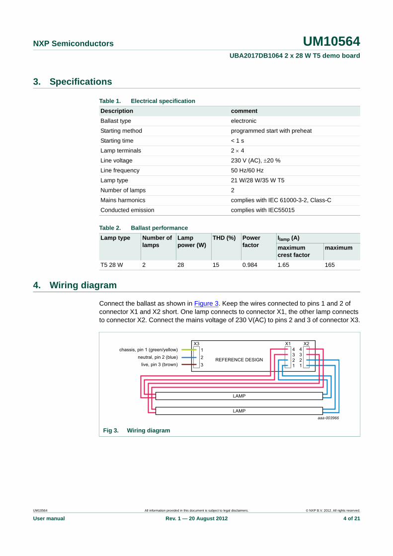
3. Specifications
4. Wiring diagram
Connect the ballast as shown in Figure 3. Keep the wires connected to pins 1 and 2 of connector X1 and X2 short. One lamp connects to connector X1, the other lamp connects to connector X2. Connect the mains voltage of 230 V(AC) to pins 2 and 3 of connector X3.
Table 1. Electrical specification
Description comment
Ballast type electronic
Starting method programmed start with preheat
Starting time < 1 s
Lamp terminals 2 4
Line voltage 230 V (AC), 20 %
Line frequency 50 Hz/60 Hz
Lamp type 21 W/28 W/35 W T5
Number of lamps 2
Mains harmonics complies with IEC 61000-3-2, Class-C
Conducted emission complies with IEC55015
Table 2. Ballast performance
Lamp type Number of lamps
Lamp power (W)
THD (%) Power factor
Ilamp (A)
maximum crest factor
maximum
T5 28 W 2 28 15 0.984 1.65 165
Fig 3. Wiring diagram
REFERENCE DESIGN
LAMP
LAMP
chassis, pin 1 (green/yellow)
neutral, pin 2 (blue)
live, pin 3 (brown)
1
2
3
X1X3 X2
1
2
3
4
1
2
3
4
aaa-003966
UM10564 All information provided in this document is subject to legal disclaimers. © NXP B.V. 2012. All rights reserved.
User manual Rev. 1 — 20 August 2012 4 of 21
NXP Semiconductors UM10564UBA2017DB1064 2 x 28 W T5 demo board
5. Board information
5.1 Block diagram
The block diagram includes the functions:
• The fuse
• ElectroMagnetic Interference (EMI) filter
• Full-wave rectifier
• Continuous Input Current (CIC) circuit
• Improved Valley Fill (IVF) circuit
• Half-bridge
• Resonant circuit
• UBA2017 half-bridge controller
5.2 Operating principle
Figure 5 is a simplified version of the complete diagram of the board. This section describes the basic functionality of the ballast.
Fig 4. Block diagram
aaa-003975
mains
voltage
inputFUSE
EMI
FILTERIVF
HALF-
BRIDGE
RESONANT
CIRCUIT
UBA2017CONTROLLER
lampsCICAC
RECTIFIER
UM10564 All information provided in this document is subject to legal disclaimers. © NXP B.V. 2012. All rights reserved.
User manual Rev. 1 — 20 August 2012 5 of 21

NXP Semiconductors UM10564UBA2017DB1064 2 x 28 W T5 demo board
5.2.1 Improved valley fill function
The topology of this board is an improved valley fill (IVF), consisting of Cvf1, Cvf2, Dvf1, Dvf2, Dvf3, Dvf4 and Cbus. The charge pump capacitors Cpump1 and Cpump2 which connect to the lamp voltage signal improve the valley fill function. Both electrolytic capacitors have a rating of 250 V. Do not exceed the maximum rating of the electrolytic capacitors. Channel F1 in Figure 5 shows the voltage across the upper electrolytic capacitor Cvf1 = C4 in the schematic when the lamp does not ignite.
Fig 5. Principle ballast schematic
lamp current senseHalf-bridge current sense
-+
Rsl
Dvf3
Cfil
Lfil
Cpump2
Cfil
Dcic2
Lr2A
Lr1A
Ccic Lamp1
Cpump1
Lamp2
Cfil
Cvf1
Cr1
Cfil
Cr2
Cdc
Cbus
Rs
Dvf2Dvf1
Lr2C
LIN
LfilLr1C
Cvf2
Lr2B
Q2
Lcic
Lfil
Q1
CIN
Dcic1
- +
Dbridge
Lr1B
Lfil
Dvf4
VIN aaa-003976
UM10564 All information provided in this document is subject to legal disclaimers. © NXP B.V. 2012. All rights reserved.
User manual Rev. 1 — 20 August 2012 6 of 21

NXP Semiconductors UM10564UBA2017DB1064 2 x 28 W T5 demo board
5.2.2 Mains harmonics
The Continuous Input Current (CIC) circuit manages the IEC mains harmonics class-C requirements. The CIC circuit consists of Dcic1, Dcic2, Lcic, Ccic. Dcic1 is a fast diode in series with the diode bridge. Dcic1 ensures a fast switch off behavior of the bridge diodes.
5.2.3 Lamp current crest factor
To meet the lamp current crest factor for IEC requirements, the lamp current control loop is used. The lamp current control loop reduces the peak of the lamp current when the mains voltage it at the maximum. The lamp current is sensed using resistor Rsense. Below 50 kHz the quasi-peak conducted emission requirements of IEC is 110 dBV. Therefore the half-bridge frequency is kept below 50 kHz, so there is headroom to allow some HF ripple in the mains current.
5.2.4 Small and low-cost half-bridge coil
If a lamp cannot ignite, the ballast generates a voltage of 750 V (RMS) which is sufficient to ignite any T5 lamp. The ignition voltage is maintained over approximate 150 ms to guarantee ignition of cold and old lamps. In this ignition phase, the LC tank inductor is saturating. The UBA2017 controller increases the half-bridge frequency instantaneously when the saturation current occurs. The level of saturation is set using a sense resistor in the source of the low side switch. Figure 7 shows the saturating current and the open lamp voltage during ignition.
(1) C1 = Vbus
(2) C2 = anode VD5
(3) F1 = VC4
(4) C4 = connector Vlamp
Fig 6. Bus voltage during open lamp ignition
UM10564 All information provided in this document is subject to legal disclaimers. © NXP B.V. 2012. All rights reserved.
User manual Rev. 1 — 20 August 2012 7 of 21

NXP Semiconductors UM10564UBA2017DB1064 2 x 28 W T5 demo board
5.2.5 Electrode/filament heating
A winding coupled to the main LC tank inductor heats each electrode. The peak of the transfer is at 90 kHz. The components Cfil and Lfil set this peak frequency. The resonance frequency of the electrode circuit (Cfil, Lfil and electrode resistance) determines this peak frequency. The UBA2017 sets the preheat frequency at 90 kHz.
There are several advantages to this type of heating circuit:
• During the preheat phase, there is enough energy to allow preheat times below 1 second.
• During the ignition phase, the load of the electrode resistance is small because of the 2nd order roll off the Cfil and Lfil filter. This feature increases the Q of the LC tank enabling either:
– a higher ignition voltage to be achieved
– the use of a smaller resonance inductor
• During normal operation, the electrode current is small at 45 kHz because of the 2nd order roll off from the Cfil and Lfil filter. This results in a lower Sum of Squares and higher ballast efficiency.
(1) C1 = Vbus.
(2) C2 = VCPT.
(3) C3 = IT2A.
(4) C4 = Vlamp(connector)
Fig 7. Open lamp ignition
UM10564 All information provided in this document is subject to legal disclaimers. © NXP B.V. 2012. All rights reserved.
User manual Rev. 1 — 20 August 2012 8 of 21

NXP Semiconductors UM10564UBA2017DB1064 2 x 28 W T5 demo board
6. Performance indicators
This section includes some of the measurements on the board. The measurements are made using an Everfine HB-6 ballast analyzer.
6.1 Mains harmonics data
(1) 2 28 W (blue).
(2) IEC limit (yellow).
Fig 8. Mains harmonics (IEC) 2 28 W T5
� �� �� �� ��
���
��� �����
� ��
���
����������
��
��
��
��
��
��
��
��
�
��
UM10564 All information provided in this document is subject to legal disclaimers. © NXP B.V. 2012. All rights reserved.
User manual Rev. 1 — 20 August 2012 9 of 21

NXP Semiconductors UM10564UBA2017DB1064 2 x 28 W T5 demo board
6.2 Input and output power versus mains input voltage
6.3 Lamp voltage and lamp current versus mains input voltage
(1) PIN (W).
(2) 2 Plamp (W).
(3) Operating frequency.
(4) Plamp (W).
Fig 9. Input power, output power and operating frequency 2 28 W T5
180 300260220 280240200
aaa-003999
40
60
70
50
30
80
20
(1)
(2)
(3)
(4)
(1) IIamp (RMS).
(2) VIamp (RMS).
Fig 10. Lamp voltage and lamp current versus mains 2 28 W T5
��� ������������ ������
����������
���
���
���
���
���
�
��
���
���
��
���
���
���
��
��
UM10564 All information provided in this document is subject to legal disclaimers. © NXP B.V. 2012. All rights reserved.
User manual Rev. 1 — 20 August 2012 10 of 21

NXP Semiconductors UM10564UBA2017DB1064 2 x 28 W T5 demo board
6.4 ElectroMagnetic Interference (EMI) prescan data
a. Line L.
b. Line N.
Fig 11. Conducted emission pre-scan test results 230 V (AC), 50 Hz, 2 28 W T5
UM10564 All information provided in this document is subject to legal disclaimers. © NXP B.V. 2012. All rights reserved.
User manual Rev. 1 — 20 August 2012 11 of 21

xxxx xxxxxxxxxxxxxxxxxxxxxxxxxxxxxx x xxxxxxxxxxxxxx xxxxxxxxxx xxx xxxxxx xxxxxxxxxxxxxxxxxxxxxxx xxxxxxxxxxxxxxxxxxxxxx xxxxx xxxxxx xx xxxxxxxxxxxxxxxxxxxxxxxxxxxxx xxxxxxxxxxxxxxxxxxxxxx xxxxxxxxxxx xxxxxxx xxxxxxxxxxxxxxxxxxx xxxxxxxxxxxxxxxx xxxxxxxxxxxxxx xxxxxx xx xxxxxxxxxxxxxxxxxxxxxxxxxxxxxxxx xxxxxxxxxxxxxxxxxxxxxxxx xxxxxxx xxxxxxxxxxxxxxxxxxxxxxxxxxxxxxxxxxxxxxxxxxxxxx xxxxxxxxxxx xxxxx x x
UM
10564
User m
anu
al
NX
P S
emico
nd
ucto
7. S
chem
atic
1 2 3 4
C1
1.8 nF
6
C2
1.8 nF
nF
L2
120 μH
L3
C5
27 nF
X1
250-204
28 W T5
T1A
D1
1N4937
3
2
+
L1
1.5 mH
4 1
T1BC3
27
R24C4
22 μF
2 mH
760800095
rsU
M10564
UB
A2
017
DB
10
64 2
x 2
8 W T
5 d
emo
bo
ard
X4
E2
6
5
1 2 3 4
5
13
4937R9
1.5 Ω
R10
1.5 Ω
IFB
L6
120 μHT2C
C15
27 nF
X2
250-204
28 W T5
120 μHT1C
F
L5
120 μH
C
C22
10 nFR18
150 kΩ
R17
150 kΩ
R16
150 kΩ
R11
150 kΩ
GND
aaa-003978
All inform
ation provided
in this docum
ent is subject to leg
al disclaim
ers.©
NX
P B
.V. 2012. A
ll rights reserved.
Rev. 1 —
20 Au
gu
st 2012
12 of 21
Fig 12. Schematic diagram
liveneutral
GHHB SHHBGLHB
EOLGLHB VFBVDD
VDD VDDSLHB EOL VFB IFB
chassis
R22
56 kΩ
R13
33 Ω
D11
1N
40
07
R12
33 kΩ
R23750 kΩ
4 1
D3
1N
40
07
D2
1N4937
3
2
D17
BAT85
D4
1N
40
07
R20 36 kΩ
C24
470 nF
C13
220 nF
E1
R19
33 kΩ
C26
82 nF
V1
V10E275P
C25
180 pF
C7
10 nFD6
1N
40
07
F1 T1A
D10
1N
40
07
+
W1X3
250-203
230 V (AC)
1 2 3
D16
1N5244B
14V
L4
2 x 39 mH6
1 3
4 UBA2017P
U1SLHB
2
3
4
5
6
7
8 9
16
15
14
13
12
11
10
D14
1N4148
C8
2.2 nF
C21
470 pFD15
1N4148
C20
100 nF
R14
33 Ω
C23
470 nF
R21
100 Ω
Q1
TK5A50DGHHB
SHHB
C10
22 nF
GLHB
SLHB
Q2
TK5A50D
C11
220 nF
R5
1 Ω
R4
1 Ω
C17
470 nF
R6
4.7 kΩR7
680 kΩ
C18
220 n
R8
22kΩ
T2A
2 mH
760800095
R2
470 k Ω
C9
4.7 nF
R3
150 kΩ
C6
4.7 nF
C27
100 nF
C16
22 μF
250 V
R25
110 kΩ
D12
1N5244B
14 V
D9
1N4148
C12
470 pFR1
180 kΩ
D8
1N
4007
1N
49
37D7
1N
493
7
D5
110 kΩ250 V
D
1N
T2BC14
27 n
C19
470 nF
VDD
Q3
BC547
chassis
IFB
EOL
VFB
1
IREF
CIFB
CF
CPT
GHHB
FSHB
SHHB
GLHB
VDD
GND
NC
PH/EN

xxxx xxxxxxxxxxxxxxxxxxxxxxxxxxxxxx x xxxxxxxxxxxxxx xxxxxxxxxx xxx xxxxxx xxxxxxxxxxxxxxxxxxxxxxx xxxxxxxxxxxxxxxxxxxxxx xxxxx xxxxxx xx xxxxxxxxxxxxxxxxxxxxxxxxxxxxx xxxxxxxxxxxxxxxxxxxxxx xxxxxxxxxxx xxxxxxx xxxxxxxxxxxxxxxxxxx xxxxxxxxxxxxxxxx xxxxxxxxxxxxxx xxxxxx xx xxxxxxxxxxxxxxxxxxxxxxxxxxxxxxxx xxxxxxxxxxxxxxxxxxxxxxxx xxxxxxx xxxxxxxxxxxxxxxxxxxxxxxxxxxxxxxxxxxxxxxxxxxxxx xxxxxxxxxxx xxxxx x x
UM
10564
User m
anu
al
NX
P S
emico
nd
ucto
8. P
CB
layou
t
rsU
M10564
UB
A2
017
DB
10
64 2
x 2
8 W T
5 d
emo
bo
ard
aaa-004346
All inform
ation provided
in this docum
ent is subject to leg
al disclaim
ers.©
NX
P B
.V. 2012. A
ll rights reserved.
Rev. 1 —
20 Au
gu
st 2012
13 of 21 Fig 13. PCB layout
a) left side of layout;mains input
b) center part of layout; UBA2017 area
c) right side of layout;lamp output

NXP Semiconductors UM10564UBA2017DB1064 2 x 28 W T5 demo board
9. Bill of materials
Table 3. Bill of materials
Part reference Description and value Part number Manufacturer
C1 capacitor; 1.8 nF; 1.6 kV B32652A1182J EPCOS
C2 capacitor; 1.8 nF; 1.6 kV B32652A1182J EPCOS
C3 film capacitor; 27 nF; 100 V ECQV1273JM Panasonic
C4 capacitor; 22 F; 250 V EEUED2E220 Panasonic
C5 capacitor; 27 nF; 100 V ECQV1273JM Panasonic
C6 capacitor; 4.7 nF; 2 kV BFC238560472 Vishay
C7 capacitor; 10 nF; 400 V BFC237051103 Vishay
C8 Y-capacitor; 2.2 nF VY2222M35Y5US63V7 Vishay
C9 capacitor; 4.7 nF; 2 kV BFC238560472 Vishay
C10 capacitor; 22 nF; 400 V BFC237051223 Vishay
C11 capacitor; 220 nF; 400 V B32562J6224K000 EPCOS
C12 ceramic disc capacitor; 470 pF; 1 kV DEBB33A471KC1B Murata
C13 capacitor; 220 nF; 400 V BFC233922224 Vishay
C14 film capacitor; 27 nF; 100 V ECQV1273JM Panasonic
C15 film capacitor; 27 nF; 100 V ECQV1273JM Panasonic
C16 capacitor; 22 F; 250 V EEUED2E220 Panasonic
C17 capacitor; 470 nF; X7R FK28X7R1C474K TDK
C18 capacitor; 220 nF; 63 V B32529C224J000 EPCOS
C19 film capacitor; 470 nF; 63 V MKS4D034703C00KSSD WIMA
C20 capacitor; 100 nF; X7R C326C104K5R5TA KEMET
C21 ceramic disc; 470 pF; 1 kV DEBB33A471KC1B Murata
C22 capacitor; 10 nF; X7R C316C103K5R5TA KEMET
C23 capacitor; 470 nF; X7R FK28X7R1C474K TDK
C24 capacitor; 470 nF; X7R FK28X7R1C474K TDK
C25 capacitor (COG); 180 pF; 5 % C315C181J1G5TA KEMET
C26 capacitor; 82 nF; X7R C320C823K5R5TA KEMET
C27 capacitor; 100 nF; X7R C326C104K5R5TA KEMET
D1 diode; 1N4937 1N4937-E3_54 Vishay
D2 diode; 1N4937 1N4937-E3_54 Vishay
D3 diode; 1N4007 1N4007-E3_54 Vishay
D4 diode; 1N4007 1N4007-E3_54 Vishay
D5 diode; 1N4937 1N4937-E3_54 Vishay
D6 diode; 1N4007 1N4007-E3_54 Vishay
D7 diode; 1N4937 1N4937-E3_54 Vishay
D8 diode; 1N4007 1N4007-E3_54 Vishay
D9 diode; 1N4148 1N4148-TR NXP Semiconductors
D10 diode; 1N4007 1N4007-E3_54 Vishay
D11 diode; 1N4007 1N4007-E3_54 Vishay
D12 diode; 1N5244B 1N5244B-TAP Vishay
UM10564 All information provided in this document is subject to legal disclaimers. © NXP B.V. 2012. All rights reserved.
User manual Rev. 1 — 20 August 2012 14 of 21

NXP Semiconductors UM10564UBA2017DB1064 2 x 28 W T5 demo board
D13 diode; 1N4937 1N4937-E3_54 Vishay
D14 diode; 1N4148 1N4148-TR NXP Semiconductors
D15 diode; 1N4148 1N4148-TR NXP Semiconductors
D16 diode; 1N5244B 1N5244B-TAP Vishay
D17 diode; BAT85 BAT85_133 NXP Semiconductors
F1 fuse; 1 A 38211000000 Littelfuse
L1 inductor; 1.5 mH RL-5480-4-1500 Renco
L2 inductor; 120 H RLB0712-121KL Bourns
L3 inductor; 120 H RLB0712-121KL Bourns
L4 inductor; 2 39 mH B82731T2551A020 EPCOS
L5 inductor; 120 H RLB0712-121KL Bourns
L6 inductor; 120 H RLB0712-121KL Bourns
Q1 transistor; TK5A50D TK5A50D Toshiba
Q2 transistor; TK5A50D TK5A50D Toshiba
Q3 transistor; BC547C BC547CBU Fairchild
R1 resistor; 180 k MRS25 Vishay
R2 resistor; 470 k MRS25000C4703FC100 Vishay
R3 resistor; 150 k MRS25000C1503FC100 Vishay
R4 resistor; 1 MRS25000C1008FC100 Vishay
R5 resistor; 1 MRS25000C1008FC100 Vishay
R6 resistor; 4.7 k MRS25000C4701FC100 Vishay
R7 resistor; 680 k MRS25000C6803FC100 Vishay
R8 resistor; 22 k MRS25000C2202FC100 Vishay
R9 resistor; 1.5 MRS25000C1508FC100 Vishay
R10 resistor; 1.5 MRS25000C1508FC100 Vishay
R11 resistor; 150 k MRS25000C1503FC100 Vishay
R12 resistor; 33 k MRS25000C3302FC100 Vishay
R13 resistor; 33 MRS25000C3309FC100 Vishay
R14 resistor; 33 MRS25000C3309FC100 Vishay
R16 resistor; 150 k MRS25000C1503FC100 Vishay
R17 resistor; 150 k MRS25000C1503FC100 Vishay
R18 resistor; 150 k MRS25000C1503FC100 Vishay
R19 resistor; 33 kv MRS25000C3302FC100 Vishay
R20 resistor; 36 k MRS25000C3602FC100 Vishay
R21 resistor; 100 k MRS25000C1000FC100 Vishay
R22 resistor; 56 k MRS25000C5602FC100 Vishay
R23 resistor; 750 k MRS25000C7503FC100 Vishay
R24 resistor; 120 k MRS25000C1203FC100 Vishay
R25 resistor; 120 k MRS25000C1203FC100 Vishay
T1 transformer; 2.0 mH 760800095 Würth Elektronik
T2 transformer; 2.0 mH 760800095 Würth Elektronik
Table 3. Bill of materials …continued
Part reference Description and value Part number Manufacturer
UM10564 All information provided in this document is subject to legal disclaimers. © NXP B.V. 2012. All rights reserved.
User manual Rev. 1 — 20 August 2012 15 of 21

NXP Semiconductors UM10564UBA2017DB1064 2 x 28 W T5 demo board
U1 Half-bridge controller IC UBA2017P/N1 NXP Semiconductors
V1 Varistor; V10E275P V10E275PL1B Littelfuse
X1 connector; 4-pin 250-204_000-009 WAGO
X2 connector; 4-pin 250-204_000-009 WAGO
X3 connector; 3-pin 250-203_000-009 WAGO
Table 3. Bill of materials …continued
Part reference Description and value Part number Manufacturer
UM10564 All information provided in this document is subject to legal disclaimers. © NXP B.V. 2012. All rights reserved.
User manual Rev. 1 — 20 August 2012 16 of 21

NXP Semiconductors UM10564UBA2017DB1064 2 x 28 W T5 demo board
10. Inductor appearance and dimensions
All dimensions in mm.
Fig 14. Half-bridge transformer appearance and dimensions
Table 4. Half-bridge transformer electrical specifications
Parameter Value
Core EE20/10/6
Inductance (4 to 1) 2.0 mH
Saturation current (4 to 1) 1.1 A
DC resistance (4 to 1) 4.95
Inductance (3 to 2) 10 H
Inductance (6 to 5) 10 H
Operating temperature 40 C to +125 C
����������������������������������
�
�
�
�
�
�
����������������������� �
�����!
�����!�����!
�������
����
���
���"
���������
�� ��� ���������
�
�
�
�
�
�
�� �����
���#������
UM10564 All information provided in this document is subject to legal disclaimers. © NXP B.V. 2012. All rights reserved.
User manual Rev. 1 — 20 August 2012 17 of 21
NXP Semiconductors UM10564UBA2017DB1064 2 x 28 W T5 demo board
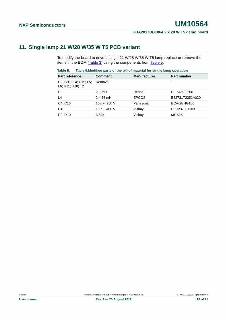
11. Single lamp 21 W/28 W/35 W T5 PCB variant
To modify the board to drive a single 21 W/28 W/35 W T5 lamp replace or remove the items in the BOM (Table 3) using the components from Table 5.
Table 5. Table 5.Modified parts of the bill of material for single lamp operation
Part reference Comment Manufacturer Part number
C2; C9; C14; C15; L5; L6; R11; R18; T2
Remove - -
L1 2.2 mH Renco RL-5480-2200
L4 2 68 mH EPCOS B82731T2351A020
C4; C16 10 F; 250 V Panasonic ECA-2EHG100
C10 10 nF; 400 V Vishay BFC237051103
R9; R10 3.3 Vishay MRS25
UM10564 All information provided in this document is subject to legal disclaimers. © NXP B.V. 2012. All rights reserved.
User manual Rev. 1 — 20 August 2012 18 of 21
NXP Semiconductors UM10564UBA2017DB1064 2 x 28 W T5 demo board
12. References
[1] UBA2017 — 600 V fluorescent lamp driver with linear dimming function
[2] UBA2017DB1064 — Demo board
[3] AN10971 — TL applications with NXP ballast controllers
[4] AN10958 — Fluorescent lamp driver with PFC using the UBA2015/16/17 family
[5] UBA2016A_15_15A — 600 V fluorescent lamp driver with PFC, linear dimming and boost function
[6] UM10561 — UBA2017AT reference design for 420 V (DC)
UM10564 All information provided in this document is subject to legal disclaimers. © NXP B.V. 2012. All rights reserved.
User manual Rev. 1 — 20 August 2012 19 of 21

NXP Semiconductors UM10564UBA2017DB1064 2 x 28 W T5 demo board
13. Legal information
13.1 Definitions
Draft — The document is a draft version only. The content is still under internal review and subject to formal approval, which may result in modifications or additions. NXP Semiconductors does not give any representations or warranties as to the accuracy or completeness of information included herein and shall have no liability for the consequences of use of such information.
13.2 Disclaimers
Limited warranty and liability — Information in this document is believed to be accurate and reliable. However, NXP Semiconductors does not give any representations or warranties, expressed or implied, as to the accuracy or completeness of such information and shall have no liability for the consequences of use of such information. NXP Semiconductors takes no responsibility for the content in this document if provided by an information source outside of NXP Semiconductors.
In no event shall NXP Semiconductors be liable for any indirect, incidental, punitive, special or consequential damages (including - without limitation - lost profits, lost savings, business interruption, costs related to the removal or replacement of any products or rework charges) whether or not such damages are based on tort (including negligence), warranty, breach of contract or any other legal theory.
Notwithstanding any damages that customer might incur for any reason whatsoever, NXP Semiconductors’ aggregate and cumulative liability towards customer for the products described herein shall be limited in accordance with the Terms and conditions of commercial sale of NXP Semiconductors.
Right to make changes — NXP Semiconductors reserves the right to make changes to information published in this document, including without limitation specifications and product descriptions, at any time and without notice. This document supersedes and replaces all information supplied prior to the publication hereof.
Suitability for use — NXP Semiconductors products are not designed, authorized or warranted to be suitable for use in life support, life-critical or safety-critical systems or equipment, nor in applications where failure or malfunction of an NXP Semiconductors product can reasonably be expected to result in personal injury, death or severe property or environmental damage. NXP Semiconductors and its suppliers accept no liability for inclusion and/or use of NXP Semiconductors products in such equipment or applications and therefore such inclusion and/or use is at the customer’s own risk.
Applications — Applications that are described herein for any of these products are for illustrative purposes only. NXP Semiconductors makes no representation or warranty that such applications will be suitable for the specified use without further testing or modification.
Customers are responsible for the design and operation of their applications and products using NXP Semiconductors products, and NXP Semiconductors accepts no liability for any assistance with applications or customer product
design. It is customer’s sole responsibility to determine whether the NXP Semiconductors product is suitable and fit for the customer’s applications and products planned, as well as for the planned application and use of customer’s third party customer(s). Customers should provide appropriate design and operating safeguards to minimize the risks associated with their applications and products.
NXP Semiconductors does not accept any liability related to any default, damage, costs or problem which is based on any weakness or default in the customer’s applications or products, or the application or use by customer’s third party customer(s). Customer is responsible for doing all necessary testing for the customer’s applications and products using NXP Semiconductors products in order to avoid a default of the applications and the products or of the application or use by customer’s third party customer(s). NXP does not accept any liability in this respect.
Export control — This document as well as the item(s) described herein may be subject to export control regulations. Export might require a prior authorization from competent authorities.
Evaluation products — This product is provided on an “as is” and “with all faults” basis for evaluation purposes only. NXP Semiconductors, its affiliates and their suppliers expressly disclaim all warranties, whether express, implied or statutory, including but not limited to the implied warranties of non-infringement, merchantability and fitness for a particular purpose. The entire risk as to the quality, or arising out of the use or performance, of this product remains with customer.
In no event shall NXP Semiconductors, its affiliates or their suppliers be liable to customer for any special, indirect, consequential, punitive or incidental damages (including without limitation damages for loss of business, business interruption, loss of use, loss of data or information, and the like) arising out the use of or inability to use the product, whether or not based on tort (including negligence), strict liability, breach of contract, breach of warranty or any other theory, even if advised of the possibility of such damages.
Notwithstanding any damages that customer might incur for any reason whatsoever (including without limitation, all damages referenced above and all direct or general damages), the entire liability of NXP Semiconductors, its affiliates and their suppliers and customer’s exclusive remedy for all of the foregoing shall be limited to actual damages incurred by customer based on reasonable reliance up to the greater of the amount actually paid by customer for the product or five dollars (US$5.00). The foregoing limitations, exclusions and disclaimers shall apply to the maximum extent permitted by applicable law, even if any remedy fails of its essential purpose.
Translations — A non-English (translated) version of a document is for reference only. The English version shall prevail in case of any discrepancy between the translated and English versions.
13.3 TrademarksNotice: All referenced brands, product names, service names and trademarks are the property of their respective owners.
UM10564 All information provided in this document is subject to legal disclaimers. © NXP B.V. 2012. All rights reserved.
User manual Rev. 1 — 20 August 2012 20 of 21

NXP Semiconductors UM10564UBA2017DB1064 2 x 28 W T5 demo board
14. Contents
1 Introduction . . . . . . . . . . . . . . . . . . . . . . . . . . . . 3
2 Safety warning . . . . . . . . . . . . . . . . . . . . . . . . . . 3
3 Specifications. . . . . . . . . . . . . . . . . . . . . . . . . . . 4
4 Wiring diagram. . . . . . . . . . . . . . . . . . . . . . . . . . 4
5 Board information . . . . . . . . . . . . . . . . . . . . . . . 55.1 Block diagram. . . . . . . . . . . . . . . . . . . . . . . . . . 55.2 Operating principle . . . . . . . . . . . . . . . . . . . . . . 55.2.1 Improved valley fill function . . . . . . . . . . . . . . . 65.2.2 Mains harmonics . . . . . . . . . . . . . . . . . . . . . . . 75.2.3 Lamp current crest factor . . . . . . . . . . . . . . . . . 75.2.4 Small and low-cost half-bridge coil . . . . . . . . . . 75.2.5 Electrode/filament heating . . . . . . . . . . . . . . . . 8
6 Performance indicators. . . . . . . . . . . . . . . . . . . 96.1 Mains harmonics data. . . . . . . . . . . . . . . . . . . . 96.2 Input and output power versus mains input
voltage . . . . . . . . . . . . . . . . . . . . . . . . . . . . . . 106.3 Lamp voltage and lamp current versus
mains input voltage. . . . . . . . . . . . . . . . . . . . . 106.4 ElectroMagnetic Interference (EMI) prescan
data. . . . . . . . . . . . . . . . . . . . . . . . . . . . . . . . . 11
7 Schematic. . . . . . . . . . . . . . . . . . . . . . . . . . . . . 12
8 PCB layout . . . . . . . . . . . . . . . . . . . . . . . . . . . . 13
9 Bill of materials . . . . . . . . . . . . . . . . . . . . . . . . 14
10 Inductor appearance and dimensions . . . . . . 17
11 Single lamp 21 W/28 W/35 W T5 PCB variant 18
12 References . . . . . . . . . . . . . . . . . . . . . . . . . . . . 19
13 Legal information. . . . . . . . . . . . . . . . . . . . . . . 2013.1 Definitions. . . . . . . . . . . . . . . . . . . . . . . . . . . . 2013.2 Disclaimers . . . . . . . . . . . . . . . . . . . . . . . . . . . 2013.3 Trademarks. . . . . . . . . . . . . . . . . . . . . . . . . . . 20
14 Contents . . . . . . . . . . . . . . . . . . . . . . . . . . . . . . 21
© NXP B.V. 2012. All rights reserved.
For more information, please visit: http://www.nxp.comFor sales office addresses, please send an email to: [email protected]
Date of release: 20 August 2012
Document identifier: UM10564
Please be aware that important notices concerning this document and the product(s)described herein, have been included in section ‘Legal information’.