um2176 user manual - home - stmicroelectronics 2017 docid030323 rev 3 1/33 um2176 user manual...
TRANSCRIPT

September 2017 DocID030323 Rev 3 1/33
www.st.com
UM2176 User manual
STEVAL-IPMNG3Q motor control power board based on the SLLIMM-nano™ 2nd series of IGBT IPMs
Introduction The STEVAL-IPMNG3Q is a compact motor drive power board based on SLLIMM-nano™ (small low-loss intelligent molded module) 2nd series (STGIPQ3H60T-HZ). It provides an affordable and easy-to-use solution for driving high power motors for a wide range of applications such as power white goods, air conditioning, compressors, power fans, high-end power tools and 3-phase inverters for motor drives in general. The IPM itself consists of short-circuit rugged IGBTs and a wide range of features like undervoltage lockout, smart shutdown, embedded temperature sensor and NTC, and overcurrent protection.
The main characteristics of this evaluation board are small size, minimal BOM and high efficiency. It consists of an interface circuit (BUS and VCC connectors), bootstrap capacitors, snubber capacitor, hardware short-circuit protection, fault event and temperature monitoring. In order to increase the flexibility, it is designed to work in single- or three-shunt configuration and with triple current sensing options: three dedicated onboard op-amps, an internal IPM op-amp and op-amps embedded in the MCU. The Hall/Encoder section completes the circuit.
With these advanced characteristics, the system is designed to achieve fast and accurate current feedback conditioning, satisfying the typical requirements for field-oriented control (FOC).
The STEVAL-IPMNG3Q is compatible with ST's STM32-based control board, enabling designers to build a complete platform for motor control.
Figure 1: Motor control board (top view) based on SLLIMM-nano™ 2nd series

Contents UM2176
2/33 DocID030323 Rev 3
Contents
1 Key features ..................................................................................... 5
2 Circuit schematics........................................................................... 6
2.1 Schematic diagrams .......................................................................... 7
3 Main characteristics ...................................................................... 12
4 Filters and key parameters ........................................................... 13
4.1 Input signals .................................................................................... 13
4.2 Bootstrap capacitor ......................................................................... 13
4.3 Overcurrent protection .................................................................... 14
4.3.1 SD pin ............................................................................................... 14
4.3.2 Shunt resistor selection .................................................................... 15
4.3.3 CIN RC filter ..................................................................................... 16
4.3.4 Single- or three-shunt selection ........................................................ 16
5 Current sensing amplifying network ............................................ 17
6 Temperature monitoring ............................................................... 19
6.1 NTC Thermistor ............................................................................... 19
7 Firmware configuration for STM32 PMSM FOC SDK .................. 20
8 Connectors, jumpers and test pins .............................................. 21
9 Bill of materials .............................................................................. 24
10 PCB design guide .......................................................................... 27
10.1 Layout of reference board ............................................................... 27
11 Recommendations and suggestions ........................................... 29
12 General safety instructions .......................................................... 30
13 References ..................................................................................... 31
14 Revision history ............................................................................ 32
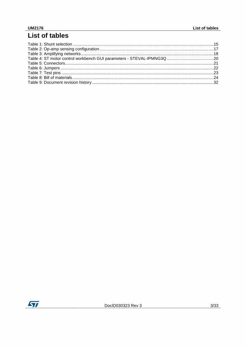
UM2176 List of tables
DocID030323 Rev 3 3/33
List of tables
Table 1: Shunt selection ........................................................................................................................... 15 Table 2: Op-amp sensing configuration .................................................................................................... 17 Table 3: Amplifying networks .................................................................................................................... 18 Table 4: ST motor control workbench GUI parameters - STEVAL-IPMNG3Q ......................................... 20 Table 5: Connectors .................................................................................................................................. 21 Table 6: Jumpers ...................................................................................................................................... 22 Table 7: Test pins ..................................................................................................................................... 23 Table 8: Bill of materials............................................................................................................................ 24 Table 9: Document revision history .......................................................................................................... 32

List of figures UM2176
4/33 DocID030323 Rev 3
List of figures
Figure 1: Motor control board (top view) based on SLLIMM-nano™ 2nd series ........................................ 1 Figure 2: Motor control board (bottom view) based on SLLIMM-nano™ 2nd series .................................. 5 Figure 3: STEVAL-IPMNG3Q circuit schematic (1 of 5) ............................................................................. 7 Figure 4: STEVAL-IPMNG3Q circuit schematic (2 of 5) ............................................................................. 8 Figure 5: STEVAL-IPMNG3Q circuit schematic (3 of 5) ............................................................................. 9 Figure 6: STEVAL-IPMNG3Q circuit schematic (4 of 5) ........................................................................... 10 Figure 7: STEVAL-IPMNG3Q circuit schematic (5 of 5) ........................................................................... 11 Figure 8: STEVAL-IPMNG3Q architecture ............................................................................................... 12 Figure 9: CBOOT graph selection ............................................................................................................ 14 Figure 10: One-shunt configuration .......................................................................................................... 16 Figure 11: Three-shunt configuration ........................................................................................................ 16 Figure 12: NTC voltage vs temperature .................................................................................................... 19 Figure 13: Silk screen and etch - top side ................................................................................................ 27 Figure 14: Silk screen and etch - bottom side .......................................................................................... 28

UM2176 Key features
DocID030323 Rev 3 5/33
1 Key features
Input voltage: 125 - 400 VDC
Nominal power: up to 300 W
Nominal current: up to 1.8 A
Input auxiliary voltage: up to 20 VDC
Motor control connector (32 pins) interfacing with ST MCU boards
Single- or three-shunt resistors for current sensing (with sensing network)
Three options for current sensing: external dedicated op-amps, internal SLLIMM-nano op-amp (single) or through MCU
Overcurrent hardware protection
IPM temperature monitoring and protection
Hall sensors (3.3 / 5 V)/encoder inputs (3.3 / 5 V)
IGBT intelligent power module:
SLLIMM-nano™ 2nd series IPM (STGIPQ3H60T-HZ - Full molded package package)
Universal design for further evaluation with bread board and testing pins
Very compact size
Figure 2: Motor control board (bottom view) based on SLLIMM-nano™ 2nd series

Circuit schematics UM2176
6/33 DocID030323 Rev 3
2 Circuit schematics
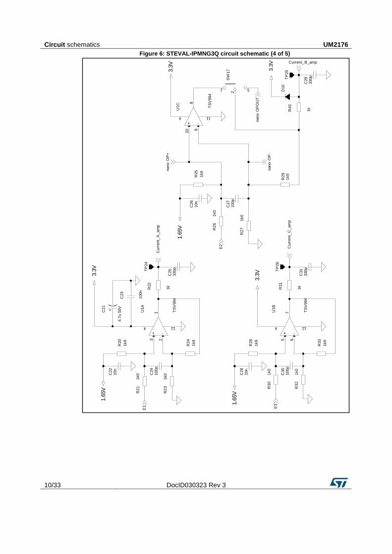
The full schematics for the SLLIMM-nano™ 2nd series card for STGIPQ3H60T-HZ IPM products is shown below. This card consists of an interface circuit (BUS and VCC connectors), bootstrap capacitors, snubber capacitor, short-circuit protection, fault output circuit, temperature monitoring, single-/three-shunt resistors and filters for input signals. It also includes bypass capacitors for VCC and bootstrap capacitors. The capacitors are located very close to the drive IC to avoid malfunction due to noise.
Three current sensing options are provided: three dedicated onboard op-amps, one internal IPM op-amp and the embedded MCU op-amps; selection is performed through three jumpers.
The Hall/Encoder section (powered at 5 V or 3.3 V) completes the circuit.

UM2176 Circuit schematics
DocID030323 Rev 3 7/33
2.1 Schematic diagrams
Figure 3: STEVAL-IPMNG3Q circuit schematic (1 of 5)
Inp
ut
DC
_bus_vol
tage
ST
EV
AL-I
PM
Nntm
p d
ecode
r
t m p
GM
01
23
56
7
4
89
NQ
3.3
V
+B
us
3.3
V 1.6
5V
Bus_voltage
RC
60
RC
12
0
RC
14
002
CR
D1
RC
10
+C
447µ/3
5V
J1
INP
UT
-dc
1 2
RC
10
0
RC
70
R2
470K
R3
120R
R1
470K
R6
1k0
-+
U1D
TS
V994
12
13
14
4 11
RC
13
0
RC
30
RC
80
RC
11
0
RC
40
+C
347µ/3
5V
R4
7k5
C2
10n RC
50
RC
90
+
C1
330µ/4
00V
R5
1k0

Circuit schematics UM2176
8/33 DocID030323 Rev 3
Figure 4: STEVAL-IPMNG3Q circuit schematic (2 of 5)
phase
_A
phase
_B
phase
_C
3.3
V+5V
EM
_S
TO
PP
WM
-A-H
PW
M-A
-LP
WM
-B-H
PW
M-B
-LP
WM
-C-H
PW
M-C
-L
NT
C_
byp
ass_re
lay
PW
M_
Vre
fM
_phase
_A
M_
phase
_B
Bus_volta
ge
M_
phase
_C
NT
C
Curr
ent_
B_
am
pE2
Curr
ent_
C_
am
p
E3
Curr
ent_
A_
am
p
E1
J3
Moto
rO
utp
ut
123
SW
2
1
2
3
SW
3
1
2
3
J2
Contr
olC
onnecto
r
12
34
56
78
910
11
12
13
14
15
16
17
19
21
23
25
26
27
28
29
30
31
32
33
34
18
20
22
24
SW
1
1
2
3
Curr
ent_
A
Curr
ent_
B
Curr
ent_
C

UM2176 Circuit schematics
DocID030323 Rev 3 9/33
Figure 5: STEVAL-IPMNG3Q circuit schematic (3 of 5)
Ph
ase
C -
in
put
Ph
ase
B -
in
put
Ph
ase
A -
in
put
IPM
mo
du
le
1_
SH
UNT
1_
SH
UN
T
3_SHUNT
3_SHUNT
+B
us
pha
se_
C
pha
se_
B
pha
se_
A
3.3
V
PW
M-C
-H
PW
M-C
-L
PW
M-B
-H
PW
M-B
-L
PW
M-A
-H
PW
M-A
-L
EM
_S
TO
P
E3
E2
E1
NT
C
nano
OP
OU
T
nano
OP
+
nano
OP
-
TP
16
SW
6
U2
ST
GIP
Q3
H60
T-H
Z
P18
HIN
W4
VccW
3
LIN
V11
VccV
9
HIN
V10
CIN
12
LIN
U16
VC
CU
13
HIN
U14
T/S
D/O
D1
15
GN
D1
T/S
D/O
D2
LIN
W5
OP
+6
OP
OU
T7
OP
-8
U,O
UT
U19
NU
20
Vboo
tV21
V,O
UT
V22
NV
23
Vboo
tW24
W,
OU
TW
25
NW
26
VbootU
17
TP
19
TP
27
C1
8
3.3
n
TP
21
D7
MM
SZ
5250
B
R1
0
1k0
R1
8
0.2
1W
C1
3100
n
R7
1k0
TP
4
SW
5
C1
010
p
TP
11
R1
25
k6
TP
18
R1
51
k0
TP
3
D9
MM
SZ
5250
B
C1
410
p
TP
5
R1
91
k0
C8
1n
C1
610
p
R9
1k0
D2
LE
DR
ed
R1
1
4k7
TP
6
R1
31
k0
D3
D6
MM
SZ
5250
B
R1
41
k0
C1
110
p
C1
510
p
C6
2.2
u
TP
20
R1
6
0.2
1W
C1
7
0,1
uF
-400
V
TP
13
TP
12
TP
17
TP
22
TP
7
J4
15
V 12
D5
C1
910
p
C5
2.2
u
SW
7S
W8
TP
9
TP
15
TP
10
R1
7
0.2
1W
TP
23
D4
TP
2
D8
MM
SZ
5250
B
SW
4
TP
8
R8
1k0
C7
2.2
u
TP
14
+C
12
10u
50
V
TP
1
Circuit schematics UM2176
10/33 DocID030323 Rev 3
Figure 6: STEVAL-IPMNG3Q circuit schematic (4 of 5)
3.3
V
1.6
5V
1.6
5V
1.6
5V
3.3
V
3.3
V
3.3
V
E1
Cu
rrent_
A_am
p
E2
Current_B_amp
E3
Cu
rrent_
C_am
p
nano
OP
+
nano
OP
-
nano
OP
OU
T
R2
11
k0
R20
1k9
-+
U1A
TS
V994
3 21
4 11
TP
24
R22
1k
R33
1k9
C30
100p
R2
71
k0
C29
330p
R31
1k
C24
100p
C28
10n
C25
330p
TP
25
-+
U1B
TS
V994
5 67
4 11
R2
61
k0
C23
100n
C22
10n
R25
1k9
D10
R24
1k9
R3
21
k0
C31
330pTP
26
SW
17
1
2
3
R2
31
k0
R29
1k9
+
C21
4.7
u 5
0V
C27
100p
-+
U1C
TS
V994
10 9
8
4 11
R3
01
k0
R28
1k9
C26
10n
R43
1k

UM2176 Circuit schematics
DocID030323 Rev 3 11/33
Figure 7: STEVAL-IPMNG3Q circuit schematic (5 of 5)
H3/
Z+
H2/
B+
H1/
A+
GN
D+
3.3
/5V
Hall/
Enco
der
M_
ph
ase
_A
M_
ph
ase
_C
M_
ph
ase
_B
3.3
V
+5V
3.3
V
+5V
R4
2
4k7
R3
92
k4
J5
En
co
de
r/H
all
11
22
33
44
55
SW
12
C3
7
10
p
SW
15
C3
4
10
0n
SW
13
SW
10
R4
04
k7
SW
9
1
2
3
R3
44
k7
R4
14
k7
R3
54
k7
C3
31
00
n
C3
5
10
p
R3
72
k4
SW
14
R3
82
k4
C3
2
10
0n
SW
16
1
2
3
R3
64
k7
SW
11
C3
6
10
p
Main characteristics UM2176
12/33 DocID030323 Rev 3
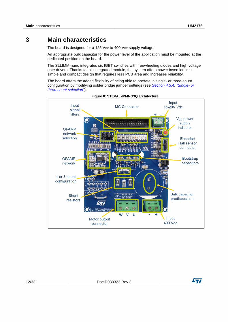
3 Main characteristics
The board is designed for a 125 VDC to 400 VDC supply voltage.
An appropriate bulk capacitor for the power level of the application must be mounted at the dedicated position on the board.
The SLLIMM-nano integrates six IGBT switches with freewheeling diodes and high voltage gate drivers. Thanks to this integrated module, the system offers power inversion in a simple and compact design that requires less PCB area and increases reliability.
The board offers the added flexibility of being able to operate in single- or three-shunt configuration by modifying solder bridge jumper settings (see Section 4.3.4: "Single- or three-shunt selection").
Figure 8: STEVAL-IPMNG3Q architecture
UM2176 Filters and key parameters
DocID030323 Rev 3 13/33
4 Filters and key parameters
4.1 Input signals
The input signals (LINx and HINx) to drive the internal IGBTs are active high. A 375 kΩ (typ.) pull-down resistor is built-in for each input signal. To prevent input signal oscillation, an RC filter is added on each input as close as possible to the IPM. The filter is designed using a time constant of 10 ns (1 kΩ and 10 pF).
4.2 Bootstrap capacitor
In the 3-phase inverter, the emitters of the low side IGBTs are connected to the negative DC bus (VDC-) as common reference ground, which allows all low side gate drivers to share the same power supply, while the emitter of the high side IGBTs is alternately connected to the positive (VDC+) and negative (VDC-) DC bus during running conditions.
A bootstrap method is a simple and cheap solution to supply the high voltage section. This function is normally accomplished by a high voltage fast recovery diode. The SLLIMM-nano 2nd series family includes a patented integrated structure that replaces the external diode with a high voltage DMOS functioning as a diode with series resistor. An internal charge pump provides the DMOS driving voltage.
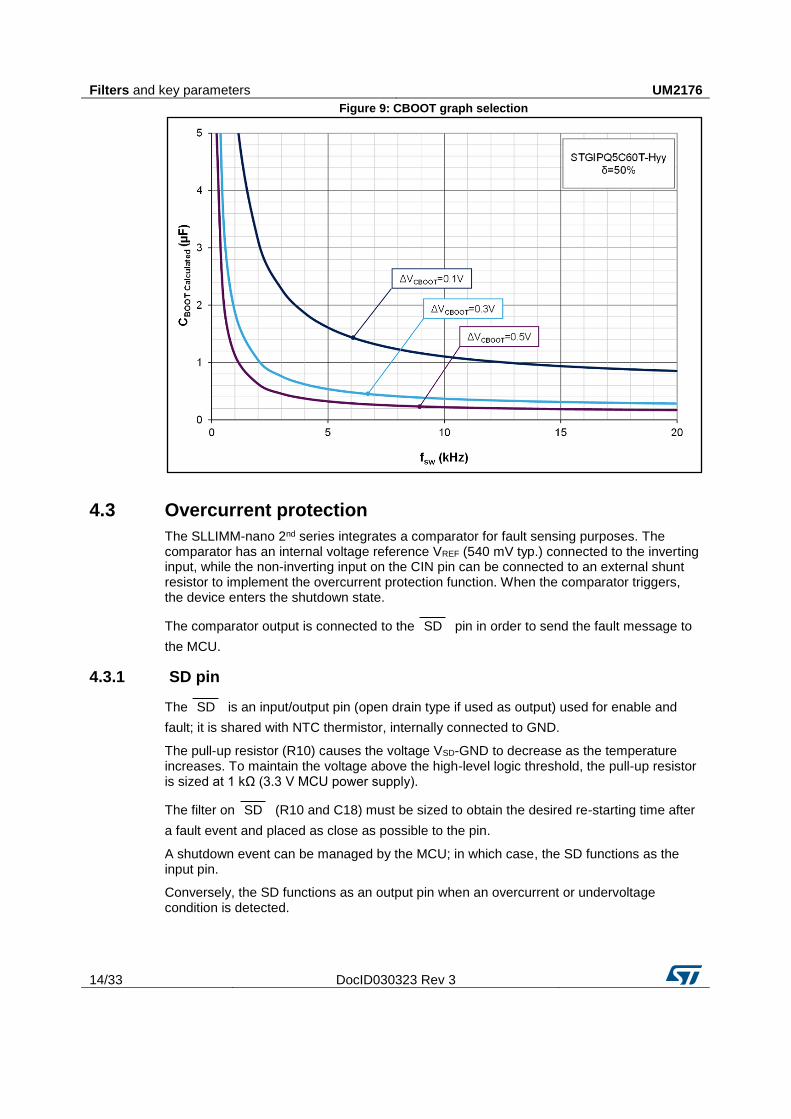
The value of the CBOOT capacitor should be calculated according to the application requirements.
Figure 9: "CBOOT graph selection" shows the behavior of CBOOT (calculated) versus switching frequency (fsw), with different values of ∆VCBOOT for a continuous sinusoidal modulation and a duty cycle δ = 50%.
This curve is taken from application note AN4840 (available on www.st.com); calculations are based on the STGIP5C60T-Hyy device, which represents the worst case scenario for this kind of calculation.
The boot capacitor must be two or three times larger than the CBOOT calculated in the graph.
For this design, a value of 2.2 µF was selected.
Filters and key parameters UM2176
14/33 DocID030323 Rev 3
Figure 9: CBOOT graph selection
4.3 Overcurrent protection
The SLLIMM-nano 2nd series integrates a comparator for fault sensing purposes. The comparator has an internal voltage reference VREF (540 mV typ.) connected to the inverting input, while the non-inverting input on the CIN pin can be connected to an external shunt resistor to implement the overcurrent protection function. When the comparator triggers, the device enters the shutdown state.
The comparator output is connected to the SD pin in order to send the fault message to
the MCU.
4.3.1 SD pin
The SD is an input/output pin (open drain type if used as output) used for enable and
fault; it is shared with NTC thermistor, internally connected to GND.
The pull-up resistor (R10) causes the voltage VSD-GND to decrease as the temperature increases. To maintain the voltage above the high-level logic threshold, the pull-up resistor is sized at 1 kΩ (3.3 V MCU power supply).
The filter on SD (R10 and C18) must be sized to obtain the desired re-starting time after
a fault event and placed as close as possible to the pin.
A shutdown event can be managed by the MCU; in which case, the SD functions as the input pin.
Conversely, the SD functions as an output pin when an overcurrent or undervoltage condition is detected.
UM2176 Filters and key parameters
DocID030323 Rev 3 15/33
4.3.2 Shunt resistor selection
The value of the shunt resistor is calculated by the following equation:
Equation 1
𝑅𝑆𝐻 =𝑉𝑟𝑒𝑓
𝐼𝑂𝐶
Where Vref is the internal comparator (CIN) (0.54 V typ.) and IOC is the overcurrent threshold detection level.
The maximum OC protection level should be set to less than the pulsed collector current in the datasheet. In this design the over current threshold level was fixed at IOC = 3.9 A in order to select a commercial shunt resistor value.
Equation 2
𝑅𝑆𝐻 =𝑉𝑟𝑒𝑓 ∙ (
𝑅15 + 𝑅11𝑅11
) + 𝑉𝐹
𝐼𝑂𝐶
=0.54 ∙ (
1000 + 47004700
) + 0.18
3.9= 0.214Ω
Where VF is the voltage drop across diodes D3, D4 and D5.
For the power rating of the shunt resistor, the following parameters must be considered:
Maximum load current of inverter (85% of Inom [Arms]): Iload(max).
Shunt resistor value at TC = 25 °C.
Power derating ratio of shunt resistor at TSH =100 °C
Safety margin.
The power rating is calculated by following equation:
Equation 3
𝑃𝑆𝐻 =1
2∙
𝐼𝑙𝑜𝑎𝑑(max)2 ∙ 𝑅𝑆𝐻 ∙ 𝑚𝑎𝑟𝑔𝑖𝑛
𝐷𝑒𝑟𝑎𝑡𝑖𝑛𝑔 𝑟𝑎𝑡𝑖𝑜
For the STGIPQ3H60T-HZ, where RSH = 0.2 Ω:
𝐼𝑛𝑜𝑚 = 3𝐴 → 𝐼𝑛𝑜𝑚[𝑟𝑚𝑠] =𝐼𝑛𝑜𝑚
√2→ 𝐼𝑙𝑜𝑎𝑑(max) = 85%(𝐼𝑛𝑜𝑚[𝑟𝑚𝑠]) = 1.8 𝐴𝑟𝑚𝑠
Power derating ratio of shunt resistor at TSH = 100 °C: 80% (from datasheet manufacturer)
Safety margin: 30%
Equation 4
𝑃𝑆𝐻 =1
2∙
1.82 ∙ 0.2 ∙ 1.3
0.8= 0.52 𝑊
Considering available commercial values, a 2 W shunt resistor was selected.
Based on the previous equations and conditions, the minimum shunt resistance and power rating is summarized below.
Table 1: Shunt selection
Device Inom (peak)
[A] OCP(peak)
[A]
Iload(max)
[Arms]
RSHUNT [Ω]
Minimum shunt power rating PSH [W]
STGIPQ3H60T-HZ
3 4.2 1.8 0.2 0.52
Filters and key parameters UM2176
16/33 DocID030323 Rev 3
4.3.3 CIN RC filter
An RC filter network on the CIN pin is required to prevent short-circuits due to the noise on the shunt resistor. In this design, the R15-C8 RC filter has a constant time of about 1 µs.
4.3.4 Single- or three-shunt selection
Single- or three-shunt resistor circuits can be adopted by setting the solder bridges SW5, SW6, SW7 and SW8.
The figures below illustrate how to set up the two configurations.
Figure 10: One-shunt configuration
Figure 11: Three-shunt configuration
Further details regarding sensing configuration are provided in the next section.

UM2176 Current sensing amplifying network
DocID030323 Rev 3 17/33
5 Current sensing amplifying network
The STEVAL-IPMNG3Q motor control demonstration board can be configured to run in three-shunt or single-shunt configurations for field oriented control (FOC).
The current can be sensed thanks to the shunt resistor and amplified by using the on-board operational amplifiers or by the MCU (if equipped with op-amp).
Once the shunt configuration is chosen by setting solder bridge on SW5, SW6, SW7 and SW8 (as described in Section 4.3.4: "Single- or three-shunt selection"), the user can choose whether to send the voltage shunt to the MCU amplified or not amplified.
Single-shunt configuration requires a single op amp so the only voltage sent to the MCU to control the sensing is connected to phase V through SW2.
SW1, SW2, SW3 and SW17 can be configured to select which signals are sent to the microcontroller, as per the following table.
Table 2: Op-amp sensing configuration
Configuration Sensing Bridge (SW1)
Bridge (SW2)
Bridge (SW3)
Bridge (SW17)
Single Shunt
IPM op-amp open 1-2 open 2-3
On board op-amp
open 1-2 open 1-2
MCU op-amp open 2-3 open 1-2
Three Shunt
On board op-amp
1-2 1-2 1-2 1-2
MCU op-amp 2-3 2-3 2-3 1-2
The operational amplifier TSV994 used on the amplifying networks has a 20 MHz gain bandwidth from a single positive supply of 3.3 V.
The amplification network must allow bidirectional current sensing, so an output offset VO = +1.65 V represents zero current.
For the STGIPQ3H60T-HZ (IOCP = 4.2 A; RSHUNT = 0.2 Ω), the maximum measurable phase current, considering that the output swings from +1.65 V to +3.3 V (MCU supply voltage) for positive currents and from +1.65 V to 0 for negative currents is:
Equation 5
𝑀𝑎𝑥𝑀𝑒𝑎𝑠𝐶𝑢𝑟𝑟𝑒𝑛𝑡 =∆𝑉
𝑟𝑚
= 4.2 𝐴
𝑟𝑚 =∆𝑉
𝑀𝑎𝑥𝑀𝑒𝑎𝑠𝐶𝑢𝑟𝑟𝑒𝑛𝑡=
1.65
4.2= 0.39 Ω
The overall trans-resistance of the two-port network is:
𝑟𝑚 = 𝑅𝑆𝐻𝑈𝑁𝑇 ∙ 𝐴𝑀𝑃 = 0.2 ∙ 𝐴𝑀𝑃 = 0.39 Ω
𝐴𝑀𝑃 =𝑟𝑚
𝑅𝑆𝐻𝑈𝑁𝑇
=0.39
0.2= 1.96
Finally choosing Ra=Rb and Rc=Rd, the differential gain of the circuit is:
𝐴𝑀𝑃 =𝑅𝑐
𝑅𝑎
= 1.9
Current sensing amplifying network UM2176
18/33 DocID030323 Rev 3
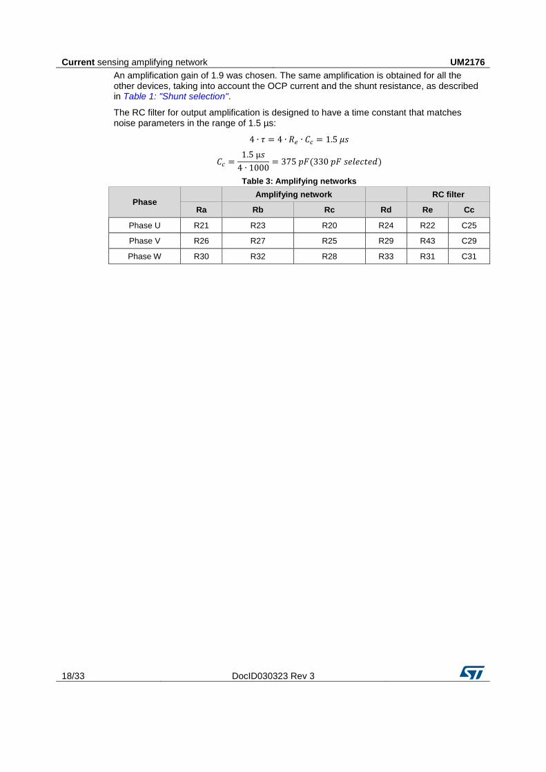
An amplification gain of 1.9 was chosen. The same amplification is obtained for all the other devices, taking into account the OCP current and the shunt resistance, as described in Table 1: "Shunt selection".
The RC filter for output amplification is designed to have a time constant that matches noise parameters in the range of 1.5 µs:
4 ∙ 𝜏 = 4 ∙ 𝑅𝑒 ∙ 𝐶𝑐 = 1.5 𝜇𝑠
𝐶𝑐 =1.5 µ𝑠
4 ∙ 1000= 375 𝑝𝐹(330 𝑝𝐹 𝑠𝑒𝑙𝑒𝑐𝑡𝑒𝑑)
Table 3: Amplifying networks
Phase Amplifying network RC filter
Ra Rb Rc Rd Re Cc
Phase U R21 R23 R20 R24 R22 C25
Phase V R26 R27 R25 R29 R43 C29
Phase W R30 R32 R28 R33 R31 C31

UM2176 Temperature monitoring
DocID030323 Rev 3 19/33
6 Temperature monitoring
The SLLIMM-nano 2nd series family integrates an NTC thermistor placed close to the power
stage. The board is designed to use it in sharing with the SD pin. Monitoring can be
enabled and disabled via the SW4 switch.
6.1 NTC Thermistor
The built-in thermistor (85 kΩ at 25 °C) is inside the IPM and connected on SD /OD pin2
(shared with the SD function).
Given the NTC characteristic and the sharing with the SD function, the network is
designed to keep the voltage on this pin higher than the minimum voltage required for the pull up voltage on this pin over the whole temperature range.
Considering Vbias = 3.3 V, a pull up resistor of 1 kΩ (R10) was used.
The figure below shows the typical voltage on this pin as a function of device temperature.
Figure 12: NTC voltage vs temperature
0.0
0.5
1.0
1.5
2.0
2.5
3.0
3.5
4.0
25 50 75 100 125
VS
D [V
]
Temperature [°C]
Vdd=3.3V
Rsd=1.0kohm
Isd (SD ON)=2.8mA
From/to mCSD/OD
M1
Smart
shut
down
VBias
RSD
CSD
SLLIMM
NTC
VSD_thL
VSD_thH
VMCU_thH
VMCU_thL
Firmware configuration for STM32 PMSM FOC SDK
UM2176
20/33 DocID030323 Rev 3
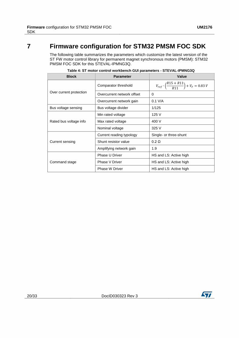
7 Firmware configuration for STM32 PMSM FOC SDK
The following table summarizes the parameters which customize the latest version of the ST FW motor control library for permanent magnet synchronous motors (PMSM): STM32 PMSM FOC SDK for this STEVAL-IPMNG3Q.
Table 4: ST motor control workbench GUI parameters - STEVAL-IPMNG3Q
Block Parameter Value
Over current protection
Comparator threshold 𝑉𝑟𝑒𝑓 ∙ (𝑅15 + 𝑅11
𝑅11) + 𝑉𝐹 = 0.83 𝑉
Overcurrent network offset 0
Overcurrent network gain 0.1 V/A
Bus voltage sensing Bus voltage divider 1/125
Rated bus voltage info
Min rated voltage 125 V
Max rated voltage 400 V
Nominal voltage 325 V
Current sensing
Current reading typology Single- or three-shunt
Shunt resistor value 0.2 Ω
Amplifying network gain 1.9
Command stage
Phase U Driver HS and LS: Active high
Phase V Driver HS and LS: Active high
Phase W Driver HS and LS: Active high
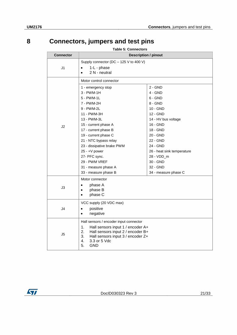
UM2176 Connectors, jumpers and test pins
DocID030323 Rev 3 21/33
8 Connectors, jumpers and test pins Table 5: Connectors
Connector Description / pinout
J1
Supply connector (DC – 125 V to 400 V)
1-L - phase
2 N - neutral
J2
Motor control connector
1 - emergency stop
3 - PWM-1H
5 - PWM-1L
7 - PWM-2H
9 - PWM-2L
11 - PWM-3H
13 - PWM-3L
15 - current phase A
17 - current phase B
19 - current phase C
21 - NTC bypass relay
23 - dissipative brake PWM
25 - +V power
27- PFC sync.
29 - PWM VREF
31 - measure phase A
33 - measure phase B
2 - GND
4 - GND
6 - GND
8 - GND
10 - GND
12 - GND
14 - HV bus voltage
16 - GND
18 - GND
20 - GND
22 - GND
24 - GND
26 - heat sink temperature
28 - VDD_m
30 - GND
32 - GND
34 - measure phase C
J3
Motor connector
phase A
phase B
phase C
J4
VCC supply (20 VDC max)
positive
negative
J5
Hall sensors / encoder input connector
1. Hall sensors input 1 / encoder A+2. Hall sensors input 2 / encoder B+3. Hall sensors input 3 / encoder Z+4. 3.3 or 5 Vdc5. GND

Connectors, jumpers and test pins UM2176
22/33 DocID030323 Rev 3
Table 6: Jumpers
Jumper Description
SW1
Choose current U to send to control board:
Jumper on 1-2: from amplification
Jumper on 2-3: directly from motor output
SW2
Choose current V to send to control board
Jumper on 1-2: from amplification
Jumper on 2-3: directly from motor output
SW3
Choose current W to send to control board:
Jumper on 1-2: from amplification
Jumper on 2-3: directly from motor output
SW4 Enable or disable sending temperature information from NTC to microcontroller
SW5, SW6
SW7, SW8
Choose 1-shunt or 3-shunt configuration.
(through solder bridge)
SW5, SW6 closed
SW7, SW8 open one shunt
SW5, SW6 open
SW7, SW8 closed three shunt
SW9, SW16
Choose input power for Hall/Encoder
Jumper on 1-2: 5 V
Jumper on 2-3: 3.3 V
SW10, SW13 Modify phase A hall sensor network
SW11, SW14 Modify phase B hall sensor network
SW12, SW15 Modify phase C hall sensor network
SW17
Choose on-board or IPM op-amp in one shunt configuration
Jumper on 1-2: on-board op-amp
Jumper on 2-3: IPM op-amp
UM2176 Connectors, jumpers and test pins
DocID030323 Rev 3 23/33
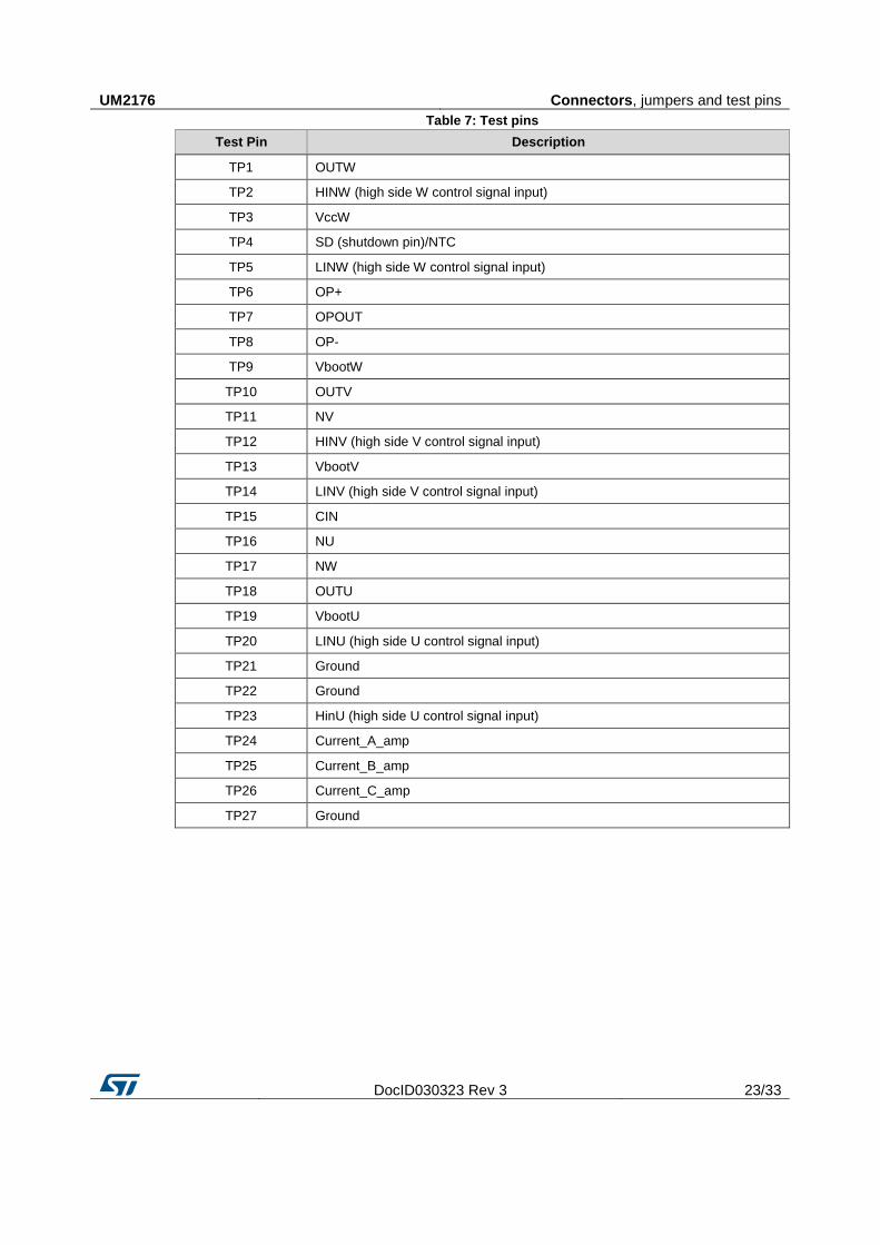
Table 7: Test pins
Test Pin Description
TP1 OUTW
TP2 HINW (high side W control signal input)
TP3 VccW
TP4 SD (shutdown pin)/NTC
TP5 LINW (high side W control signal input)
TP6 OP+
TP7 OPOUT
TP8 OP-
TP9 VbootW
TP10 OUTV
TP11 NV
TP12 HINV (high side V control signal input)
TP13 VbootV
TP14 LINV (high side V control signal input)
TP15 CIN
TP16 NU
TP17 NW
TP18 OUTU
TP19 VbootU
TP20 LINU (high side U control signal input)
TP21 Ground
TP22 Ground
TP23 HinU (high side U control signal input)
TP24 Current_A_amp
TP25 Current_B_amp
TP26 Current_C_amp
TP27 Ground

Bill of materials UM2176
24/33 DocID030323 Rev 3
9 Bill of materials Table 8: Bill of materials
Item Q.ty
Ref. Part/Value Description Manufacturer Order code
1 1 C1 330 µF 400 V ±10% Electrolytic Capacitor
EPCOS B43501A9337M000
2 5 C2, C22, C26, C28
10 nF 50 V ±10% Ceramic Multilayer Capacitors
AVX 12065C103KAT2A
3 2 C3, C4 47 µF 50 V ±20% Electrolytic Capacitor
any any
4 3 C5, C6, C7 2.2 µF 25V ±10% Ceramic Multilayer Capacitors
Murata
GCM31MR71E225KA57L
5 1 C17 0.1 µF 630V ±10% Ceramic Multilayer Capacitors
Murata
GRM43DR72J104KW01L
6 9
C10,C11,C14,C15,C16, C19,C35,C36,C37
10 pF 100 V ±10% Ceramic Multilayer Capacitors
AVX 12061A100JAT2A
7 5 C13,C23,C32,C33,C34
100 nF 50 V ±10% Ceramic Multilayer Capacitors
AVX 12065C104KAZ2A
8 1 C8 1 nF 50 V ±10% Ceramic Multilayer Capacitors
Kemet
C1206C102K5RACTU
9 1 C12 10 µF 50 V ±20% Electrolytic Capacitor
any any
10 1 C18 3.3 nF 50 V ±10% Ceramic Multilayer Capacitors
Kemet
C1206C332K5RACTU
11 3 C24,C27,C30 100 pF 100 V ±10% Ceramic Multilayer Capacitors
Kemet
C1206C101J1GACTU
12 3 C25,C29,C31 330 pF 50 V ±10% Ceramic Multilayer Capacitors
AVX 12065A331JAT2A
13 1 C21 4.7 µF 50 V ±20% Electrolytic Capacitor
any any
14 5 D1,D3,D4,D5,D10
Diode BAT48J - ST BAT48J
UM2176 Bill of materials
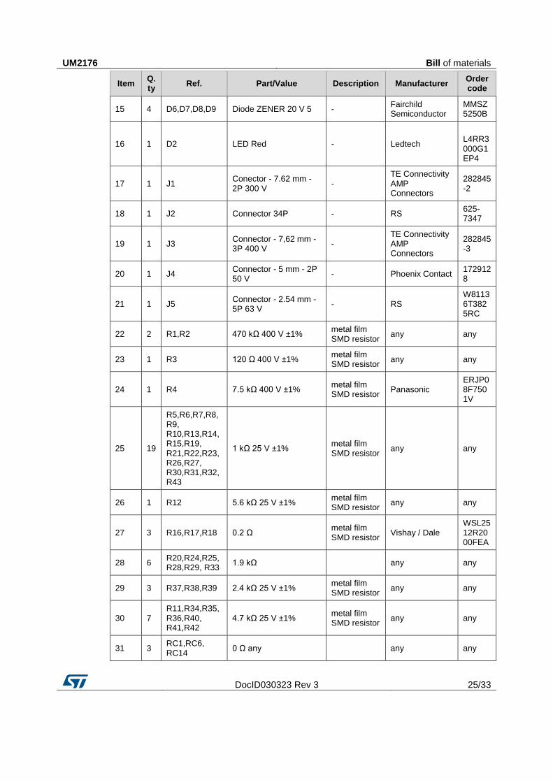
DocID030323 Rev 3 25/33
Item Q.ty
Ref. Part/Value Description Manufacturer Order code
15 4 D6,D7,D8,D9 Diode ZENER 20 V 5 - Fairchild Semiconductor
MMSZ5250B
16 1 D2 LED Red - Ledtech L4RR3000G1EP4
17 1 J1 Conector - 7.62 mm - 2P 300 V
- TE Connectivity AMP Connectors
282845-2
18 1 J2 Connector 34P - RS 625-7347
19 1 J3 Connector - 7,62 mm - 3P 400 V
- TE Connectivity AMP Connectors
282845-3
20 1 J4 Connector - 5 mm - 2P 50 V
- Phoenix Contact 1729128
21 1 J5 Connector - 2.54 mm - 5P 63 V
- RS W81136T3825RC
22 2 R1,R2 470 kΩ 400 V ±1% metal film SMD resistor
any any
23 1 R3 120 Ω 400 V ±1% metal film SMD resistor
any any
24 1 R4 7.5 kΩ 400 V ±1% metal film SMD resistor
Panasonic ERJP08F7501V
25 19
R5,R6,R7,R8,R9, R10,R13,R14,R15,R19, R21,R22,R23,R26,R27, R30,R31,R32,R43
1 kΩ 25 V ±1% metal film SMD resistor
any any
26 1 R12 5.6 kΩ 25 V ±1% metal film SMD resistor
any any
27 3 R16,R17,R18 0.2 Ω metal film SMD resistor
Vishay / Dale WSL2512R2000FEA
28 6 R20,R24,R25,R28,R29, R33
1.9 kΩ any any
29 3 R37,R38,R39 2.4 kΩ 25 V ±1% metal film SMD resistor
any any
30 7 R11,R34,R35,R36,R40, R41,R42
4.7 kΩ 25 V ±1% metal film SMD resistor
any any
31 3 RC1,RC6, RC14
0 Ω any any any
Bill of materials UM2176
26/33 DocID030323 Rev 3
Item Q.ty
Ref. Part/Value Description Manufacturer Order code
32 11
RC2,RC3,RC4,RC5,RC7, RC8,RC9,RC10,RC11,RC12, RC13
DNM
33 2 SW7,SW8 Solder Bridge - - -
34 2 SW5,SW6 open - - -
35 6 SW1,SW2,SW3,SW9, SW16,SW17
Jumper 2.54 - RS W81136T3825RC
36 7
SW4,SW10,SW11,SW12, SW13,SW14,SW15
Jumper 2.54 - RS W81136T3825RC
37 26
TP1,TP2,TP3,TP4,TP5, TP6,TP7,TP8,TP9,TP10, TP11,TP12,TP13,TP14,TP15, TP16,TP17,TP18,TP19,TP20, TP22,TP23,TP24,TP25,TP26, TP27
PCB terminal 1mm - KEYSTONE 5001
38 26 TP22,TP27 PCB terminal 1 mm - KEYSTONE 5001
39 1 TP21 PCB terminal 12.7mm HARWIN D3083B-46
40 13 to close SWxy Jumper TE Connectivity female straight, Black, 2-way, 2.54 mm
- RS 881545-2
41 1 U1 TSV994IDT - ST TSV994IDT
42 1 U2 STGIPQ3H60T-HZ ST-SUPPLY
ST-SUPPLY ST STGIPQ3H60T-HZ
UM2176 PCB design guide
DocID030323 Rev 3 27/33
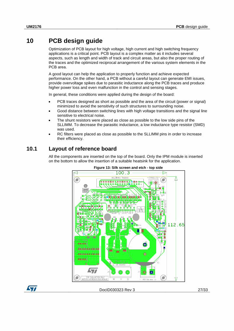
10 PCB design guide
Optimization of PCB layout for high voltage, high current and high switching frequency applications is a critical point. PCB layout is a complex matter as it includes several aspects, such as length and width of track and circuit areas, but also the proper routing of the traces and the optimized reciprocal arrangement of the various system elements in the PCB area.
A good layout can help the application to properly function and achieve expected performance. On the other hand, a PCB without a careful layout can generate EMI issues, provide overvoltage spikes due to parasitic inductance along the PCB traces and produce higher power loss and even malfunction in the control and sensing stages.
In general, these conditions were applied during the design of the board:
PCB traces designed as short as possible and the area of the circuit (power or signal)minimized to avoid the sensitivity of such structures to surrounding noise.
Good distance between switching lines with high voltage transitions and the signal linesensitive to electrical noise.
The shunt resistors were placed as close as possible to the low side pins of theSLLIMM. To decrease the parasitic inductance, a low inductance type resistor (SMD)was used.
RC filters were placed as close as possible to the SLLIMM pins in order to increasetheir efficiency.
10.1 Layout of reference board
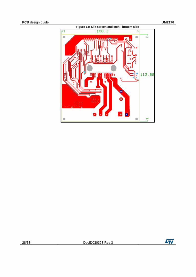
All the components are inserted on the top of the board. Only the IPM module is inserted on the bottom to allow the insertion of a suitable heatsink for the application.
Figure 13: Silk screen and etch - top side
PCB design guide UM2176
28/33 DocID030323 Rev 3
Figure 14: Silk screen and etch - bottom side
UM2176 Recommendations and suggestions
DocID030323 Rev 3 29/33
11 Recommendations and suggestions
The BOM list is not provided with a bulk capacitor already inserted in the PCB.However, the necessary space has been included (C1). In order to obtain a stable bussupply voltage, it is advisable to use an adequate bulk capacity. For general motorcontrol applications, an electrolytic capacitor of at least 100 µF is suggested.
Similarly, the PCB does not come with a heat sink. You can place one above the IPMon the back side of the PCB with thermal conductive foil and screws. RTH is animportant factor for good thermal performance and depends on certain factors such ascurrent phase, switching frequency, power factor and ambient temperature.
The board requires +5 V and +3.3 V to be supplied externally through the 34-pin motorcontrol connector J2. Please refer to the relevant board manuals for information onkey connections and supplies.

General safety instructions UM2176
30/33 DocID030323 Rev 3
12 General safety instructions
The evaluation board works with high voltage which could be deadly for the users. Furthermore all circuits on the board are not isolated from the line input. Due to the high power density, the components on the board as well as the heat sink can be heated to a very high temperature, which can cause a burning risk when touched directly. This board is intended for use by experienced power electronics professionals who understand the precautions that must be taken to ensure that no danger or risk may occur while operating this board.
After the operation of the evaluation board, the bulk capacitor C1 (if used) may still store a high energy for several minutes. So it must be first discharged before any direct touching of the board.
To protect the bulk capacitor C1, we strongly recommended using an external brake chopper after C1 (to discharge the high brake current back from the induction motor).
UM2176 References
DocID030323 Rev 3 31/33
13 References
Freely available on www.st.com:
1. STGIPQ3H60T-HZ datasheet2. TSV994 datasheet3. BAT48 datasheet4. MMSZ5250B datasheet5. UM1052 STM32F PMSM single/dual FOC SDK v4.36. AN4840 SLLIMM™-nano 2nd series small low-loss intelligent molded module

Revision history UM2176
32/33 DocID030323 Rev 3
14 Revision history Table 9: Document revision history
Date Version Changes
02-Mar-2017 1 Initial release.
17-May-2017 2
Updated Figure 1: "Motor control board (top view) based on SLLIMM-nano™ 2nd series"
In Table 4: "ST motor control workbench GUI parameters - STEVAL-IPMNG3Q", changed current sensing block amplifying network gain
parameter value to 1.9 (was 0.9)
19-Sep-2017 3 Updated Section 1: "Key features", Section 4.3.2: "Shunt resistor selection" and Section 11: "Recommendations and suggestions".
UM2176
DocID030323 Rev 3 33/33
IMPORTANT NOTICE – PLEASE READ CAREFULLY
STMicroelectronics NV and its subsidiaries (“ST”) reserve the right to make changes, corrections, enhancements, modifications, and improvements to ST products and/or to this document at any time without notice. Purchasers should obtain the latest relevant information on ST products before placing orders. ST products are sold pursuant to ST’s terms and conditions of sale in place at the time of order acknowledgement.
Purchasers are solely responsible for the choice, selection, and use of ST products and ST assumes no liability for application assistance or the design of Purchasers’ products.
No license, express or implied, to any intellectual property right is granted by ST herein.
Resale of ST products with provisions different from the information set forth herein shall void any warranty granted by ST for such product.
ST and the ST logo are trademarks of ST. All other product or service names are the property of their respective owners.
Information in this document supersedes and replaces information previously supplied in any prior versions of this document.
© 2017 STMicroelectronics – All rights reserved