understanding the structural and physical basis of selenium based semiconductor professor zainal...
TRANSCRIPT

UNDERSTANDING THE STRUCTURAL AND PHYSICAL BASIS OF SELENIUM BASED SEMICONDUCTOR
Professor Zainal Abidin Talib
Dr. Josephine Liew Ying Chyi
Professor W. Mahmood Mat Yunus

INTRODUCTION

Copper Selenide belongs to a family of chalcogenide materials has received great attention due to its particular
photoelectrical properties and wide applications in electronic and optoelectronic devices [1-12] such as:
solar cell
optical filter
photodetector
schottky-diodes
thermoelectric converter

The attraction of this binary material also depends on its feasibility to use as a precursor material to incorporate indium or other elements made available and lead to formation of ternary compound such as copper indium diselenide (CuInSe2) or other multinary material for thin film solar cell application [13-17].
It has a wide range of stoichiometric compositions (CuSe, Cu2Se, Cu3Se2, Cu7Se4, Cu5Se4, CuSe2) and non-stoichiometric composition (Cu2-xSe) [8, 18]
Copper selenide can be constructed into several well documented crystallographic (phases and structural) forms such as orthorhombic [17, 19-21], monoclinic [22], cubic [21-24], tetragonal [17, 21], hexagonal [24-26] etc depending on their compositions form by various preparation technique [22, 27].

Tin Selenide (SnSe) Tin Selenide is a p-type (IV-VI) semiconductor with attractive electronic and
optical properties [1, 28-38] which bring numerous applications such as:
Photovoltaic system Radiation detector
Memory switching devices
Holographic recording systems
Lithium intercalation batteries
Thermoelectric cooling
Infrared optoelectroni
c devices

Tin Selenide are classified as narrow-gap semiconductors (bandgap 1 – 2 eV) and are capable of absorbing major part of solar energy for photovoltaic applications[1, 28, 39, 40].
Tin monoselenide is a p-type semiconductor with an orthorhombic structure.
The tin(II) selenide crystals are construct by tightly bound layers which formed by double planes with zigzag chains of tin and selenium atoms[41].
The highly layered structure, typical of all orthorhombic chlacogenide crystals, causes a strong anisotropy of physical properties of tin(II) selenide.
Because of their anisotropic character, the tin (II) selenide chalcogenides becomes an attractive layered compounds, and can be used as cathode materials in lithium intercalation batteries[42].
Copper Tin Selenide (Cu2SnSe3)
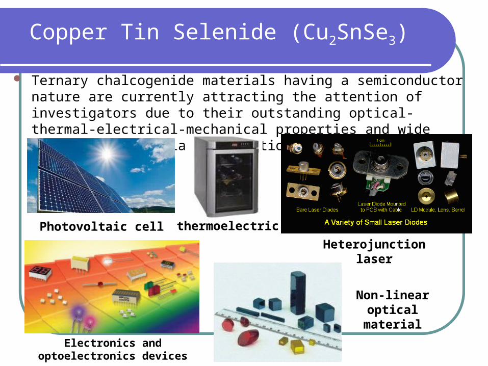
Ternary chalcogenide materials having a semiconductor nature are currently attracting the attention of investigators due to their outstanding optical-thermal-electrical-mechanical properties and wide variety of potential applications in the fields like [43 – 52]:
Photovoltaic cell thermoelectric
Electronics and optoelectronics devices
Non-linear optical material
Heterojunction laser
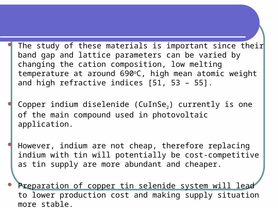
The study of these materials is important since their band gap and lattice parameters can be varied by changing the cation composition, low melting temperature at around 690oC, high mean atomic weight and high refractive indices [51, 53 – 55].
Copper indium diselenide (CuInSe2) currently is one of the main compound
used in photovoltaic application. However, indium are not cheap, therefore replacing indium with tin will
potentially be cost-competitive as tin supply are more abundant and cheaper.
Preparation of copper tin selenide system will lead to lower production cost and making supply situation more stable.

Nickel Selenide , a p-type semiconductor with a band-gap of 620nm (2.0eV) reveals significant electronic and magnetic properties.
NiSe is formed from Nickel and Selenium due to the valence electronic configuration of Ni (3d84s2) and the small difference in electronegativity between Ni (χ = 1.9) and Se (χ = 2.4)
NICKEL SELENIDE (NiSe)

IRON SELENIDE (FeSe2)
• Semiconductors
• Potential material for future applications in magnetoelectronics
• Potential material for future applications in optoelectronic devices

ZINC SELENIDE (ZnSe)
• ZnSe is good candidates for applications in various optoelectronic devices such as light emitting diodes (LED), semiconductor laser and photodetector.
• This is because of the nanometer size structure makes the electronic energy state discrete.
• When the diameter of nanocrystals is decreased, the energy separation and quantum effect will be enhanced.

OBJECTIVE
Fabrication of selenium based semiconductor (CuSe, SnSe, NiSe2, Cu2SnSe3) in powder form (compositional analysis) and thin film (deposition condition analysis).
Optical, electrical and thermal properties
characterization of the Se based semiconductor.
Evaluate the temperature dependence of the selenium based semiconductor from the observation of structural, electrical, optical and thermal properties changes at various temperature.

IMPORTANT OF STUDIES It is evident that for the future well-being of nations, a supply of energy based
on a renewable source which is economically and environmentally acceptable has to be developed.
Successful production of an efficient metal chalcogenide solar cell and modules requires the coupling of fabrication techniques with a basic understanding of the devices.
There is a need to develop a greater fundamental sciences and engineering basis for the selenium based semiconductor material devices and processing requirement.
In this work, we have fill the information gap on literature about the fundamental study of the structural, electrical, thermal and optical studies in polycrystalline CuSe, SnSe, NiSe2, ZnSe, FeSe2 and Cu2SnSe3 material.
This fundamental knowledge will guide us to find out the fabrication and design parameters, which are imposed by current technology, material specifications and irradiation conditions to maximize the solar cell efficiency.

Sample Preparation
Powder preparation – Chemical Precipitation TechniquePellet preparation – Moulding
Thin film preparation – Thermal Evaporation Technique

CuSe Powder Preparation
Chemical Precipitation Method
Selenium alkaline aqueous solution (12 M NaOH + 3.948 g Se) (Solution A) Stirred for 2 hours
Mixture stirred for 24 hours
Black precipitate obtained
Dried in oven ( 70oC) for 24 hr
Structural studies by XRD Pressed into pellet
CuCl22H2O solution (solution B)
Centrifuge and wash in distill water

20 25 30 35 40 45 50 55 60
0.02 mol CuCl2.H
2O
0.03 mol CuCl2.H
2O
0.04 mol CuCl2.H
2O
0.05 mol CuCl2.H
2O
0.06 mol CuCl2.H
2O
CuSe
0.09 mol CuCl2.H
2O
Cu3Se
2Cu2Se
Inte
nsi
ty (
Arb
. Un
it)
Position ()
Se
We found that by using the
concentration of 0.03 mol
CuCl22H2O, the CuSe powder
with high purity has been
successfully produced.
XRD pattern of CuSe Sample prepared at different Molarity of CuCl2.H2O

20 25 30 35 40 45 50 55 60
0
1000
2000
3000
4000
5000
6000
7000
8000
Inte
nsi
ty (
Arb
. Un
it)
Position (2)
106
116
202
108
110
006
102
101
100
All the peaks obtained are well matched with the JCPDS data (File No. 34-0171) as Klockmannite, syn which belongs to the hexagonal system.
Orientation along (102) plane was found to be most prominent.
XRD Spectra of synthesized CuSe powder

EDX spectrum for synthesized CuSe powder
• There are three prominent peaks corresponding to the Cu, Se and Au element.
• The Au signal detected in the EDX spectrum is the results of gold coating on sample to prevent charging.
• small signal of C and O observed is expected from the background environment and carbon tape holding the powder sample.
• There are no other impurities elements were found by EDX spectrum.

Synthesis SnSe PowderChemical Precipitation Method
Selenium alkaline aqueous solution (0.56 mol NaOH + 1.974 g Se)
(Solution A) (50 ml water)Stirred for 2 hours
Tin (II) complex aqueous Solution(SnCl2 + 9 g tartaric acid)
(solution B)Stirred for 2 hours
Mixture stirred for 24 hours
Black precipitate obtained
wash in sequence using membrane filter
Dried in oven ( 70oC)
Structural studies by XRD Moulding into pellet
centrifuge

20 25 30 35 40 45 50 55 60
mol SnCl2
mol SnCl2
mol SnCl2
mol SnCl2
mol SnCl2
mol SnCl2
mol SnCl2
SeIn
ten
sity
(A
rb.U
nit)
Position (2)
XRD pattern of SnSe Sample prepared at different molarity of SnCl2

XRD Spectra of synthesized SnSe powder
20 25 30 35 40 45 50 55 60
0
2000
4000
6000
8000
10000
Inte
nsi
ty (
Arb
. Uni
t)
Position (242
0
402
511
30241
1
102
311
400
111
011
201
All the peaks obtained are well matched with the JCPDS data (File No. 32-1382) which belongs to the orthorhombic system.
Orientation along (111) plane was found to be most prominent.
The sharp peaks obtained indicate that the material produced is of high crystallinity.

EDX spectrum for synthesized SnSe powder
Strong peaks corresponding to Sn, Se and Au element are found in the spectrum, and no impurity peaks are detected in the EDX spectrum.
The Au peak observed in the EDX spectrum is due to the gold sputtering coating on the sample to prevent charging while the carbon and oxygen peaks are due to the dissolved atmospheric CO2 or carbon tape holding the powder sample.
The elemental analysis was carried out only for Sn and Se element and the average atomic percentage of Sn:Se is 52.36 : 47.64 in the ratio range 1.1 : 1 which is nearly stoichiometry and close to the expected value of 1:1 (SnSe) in agreement with the XRD data.

To study the effects of concentration NiCl2·6H2O in synthesizing NiSe
Mass of the Se powder
was weighted
Mass of NiCl2·6H2O was weighted
Both mass were put together in a
beaker
Ethylenediamine were added
into the beaker
The solution were poured
into the Teflon lined autoclave
The autoclave were put into the oven for 180 C for 6 ⁰
hours

XRD patterns of NiSe2 compound synthesized using different concentration of NiCl2·6H2O

XRD Spectra of synthesized NiSe2 powder
• All the peaks obtained are well matched with the JCPDS data (File No. 98-010-1405), Nickel (IV) Selenide which belongs to the cubic system.
• The sharp peaks obtained indicate that the material produced is of high crystallinity.

Synthesis of ZnSe Compound


XRD pattern of ZnSe synthesized with different ratio ZnCl2/Se

• All the peaks obtained are well matched with the JCPDS data (File No. 98-009-1262), stilleite which belongs to the cubic system.
• The sharp peaks obtained indicate that the material produced is of high crystallinity.
XRD Spectra of synthesized ZnSe powder

Synthesis of FeSe2 sample

40 ml of distilled water was prepared .
3 ml of N2H4•H2O was prepared.
Na2SeO3 and FeCl3•6H2O was prepared.
All the starting materials were added into distilled water and stir for 3 minutes at 6 rpm.
The sample was transferred into 50 ml Stainless Teflon-lined autoclave and heated up at 140°C for 12 hours.

The sample was filtered with distilled water in a centrifuge for 15 times.
The sample was dry in an oven at 60°C for 48 hours.
The sample was grind with pestle and mortar into powder form.
The sample was weight and transferred to a sample bottle.

The FeSe2 peaks in the entire pattern obtained can be identified as orthorhombic FeSe2 with lattice constant a=4.80 Å, b=5.78 Å, c=3.58 Å, which matched the value in the standard data (ICSD, 98-004-8006).
Other oxides formed are Fe3O4 (ICSD, 98-001-7319) and Fe2O3 (ICSD, 98-009-6377).
XRD patterns of FeSe2 compound synthesized using different concentration of NiCl2·6H2O

Schematic flow chart for the Cu2SnSe3 nanoparticles preparation
Chemical Precipitation Method
selenium alkaline aqueous solution
Se + NaOHto produce Se2- and ions
Stirred for 2 hours
Mixture stir for 24 hoursprecipitate obtained
Dried in oven ( 70oC) for 24 hr
Cu (II) tartrate complex solution(0.015, 0.030, 0.045, 0.060, 0.068,
0.075, 0.083, 0.090, 0.120 and 0.150 mol) CuCl2∙2H2O + tartaric acid
Stirred for 2 hours
Centrifuge and wash in distill water
23SeO
Tin (II) complex aqueous solution
0.078 mol SnCl2∙2H2O + tartaric acid
Stirred for 2 hours
pH control
Grinding powder using mortar and pestle

20 25 30 35 40 45 50 55 60
2000
4000
6000
8000
10000
12000
14000
SnSe CuSe
0.068 mol CuCl2.2H
2O
0.060 mol CuCl2.2H
2O
0.045 mol CuCl2.2H
2O
0.030 mol CuCl2.2H
2O
Inte
nsity
(A
rb. U
nit)
Position (2 Theta)
0.015 mol CuCl2.2H
2O
Cu2SnSe
3
20 25 30 35 40 45 50 55 600
2000
4000
6000
8000
10000
12000
14000
16000
o
o
o
o
CuSe
Cu
2SnSe
3* Cu
3Se
2
0.150 mol CuCl2.2H
2O
0.090 mol CuCl2.2H
2O
0.120 mol CuCl2.2H
2O
0.083 mol CuCl2.2H
2O
0.075 mol CuCl2.2H
2O
0.068 mol CuCl2.2H
2O
Inte
nsi
ty (
Arb
. Un
it)
Position (2Theta
o Se
XRD pattern of the copper tin selenide powder synthesized by controlling the concentration of copper chloride (CuCl22H2O) from 0.015 to 0.150 mol with the
concentration of tin chloride (SnCl2∙2H2O) and Se fixed at 0.078 and 0.025 mol respectively
• The XRD results show that when excessive CuCl22H2O was added, the final product is a mixture of Cu3Se2, CuSe and Cu2SnSe3.
• Less CuCl22H2O concentration will lead to formation of SnSe and Cu2SnSe3 mixture.
• All these results indicate that the binary compounds such as CuSe and SnSe will become intermediates during the formation of product Cu2SnSe3.
• 0.068 mol CuCl2.2H2O concentration has been chosen as the optimum amount to further test on the pH condition

20 25 30 35 40 45 50 55 60
0
2000
4000
6000
8000
10000
12000
14000
16000
18000
20000
Cu3Se
2
SnSe
Cu2SnSe3
pH 0.84
pH 1.09
pH 1.30
pH 1.58
pH 1.65
pH 1.77
pH 1.90
pH 3.63
Inte
nsi
ty (
Arb
. Un
it)
Position (2)
pH 6.51
XRD pattern of copper tin selenide powder synthesized at different pH condition (pH 0.84, 1.09, 1.30. 1.58, 1.65, 1.77, 1.90, 3.63,
6.51) with 0.068 mol CuCl22H2O, 5.2 M SnCl2∙2H2O and 0.5 M Se concentration
the growth solution of pH at 1.30 is the optimum acidity condition which favors the formation of Cu2SnSe3 phase without any other impurities.
20 30 40 50 60 70 80
0
1000
2000
3000
4000
33
1
40
0
31
1
22
0
Inte
nsi
ty (
Arb
. Un
it)
Position 2
11
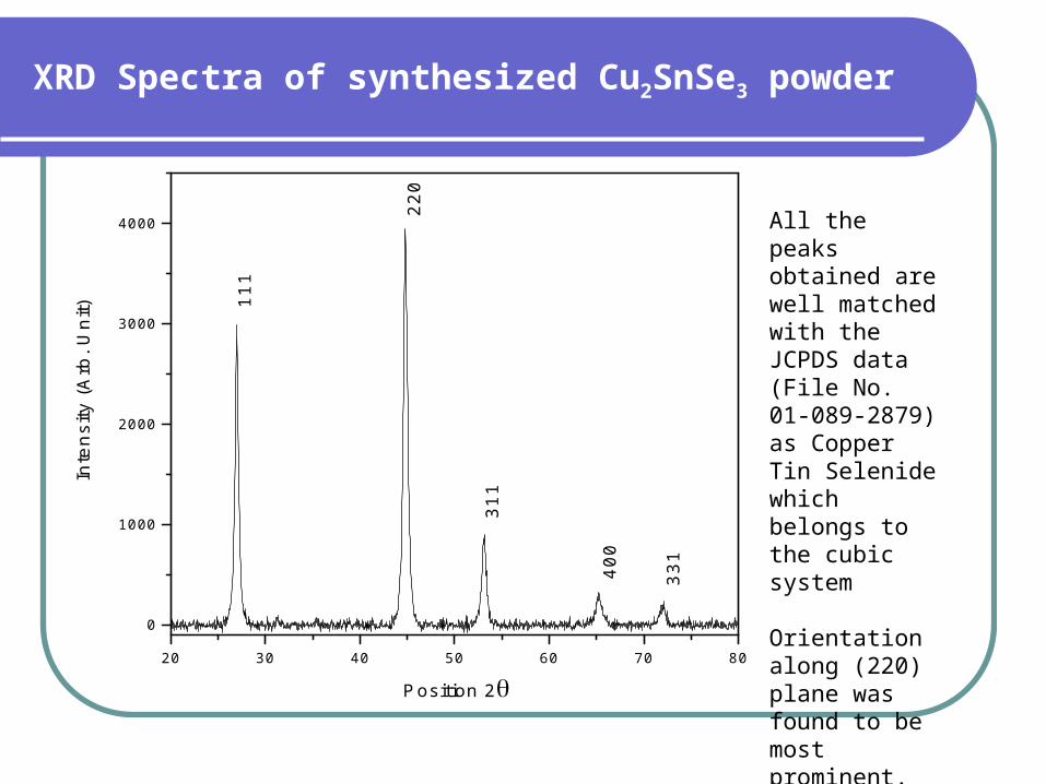
1All the peaks obtained are well matched with the JCPDS data (File No. 01-089-2879) as Copper Tin Selenide which belongs to the cubic system
Orientation along (220) plane was found to be most prominent.
XRD Spectra of synthesized Cu2SnSe3 powder

EDX spectrum of synthesized Cu2SnSe3 powder
• The results show the prominent peaks in the EDX spectrum are attributed to Cu (34.54%), Sn (18.48%) and Se (46.97%).
• The Au signal detected in the EDX spectrum is the results of gold sputtering on powder sample to prevent charging while the carbon and oxygen signal are expected due to the dissolved atmospheric CO2 or carbon tape holding the powder samples.
• No other impurity elements are found in the EDX spectrum. • The calculated average atomic ratio of Cu:Sn:Se appears to be nearly stoichiometric (2.1 :
1.1 : 2.9) which is close to the expected value of (2 : 1 : 3) the nominal composition of Cu2SnSe3 as suggested by the XRD study.

Methodology
Combination of evacuated quartz ampoule & modified rocking furnace
Source material
+Evacuated ampoule
Evacuated ampoule
‘A furnace for producing chalcogenide based alloy and a method for producing thereof’ by Talib, Z. A., Sabli, N., Yunus, W. M. M., Shaari, A. H. (MyIPO Paten Pending: PI2012700841)
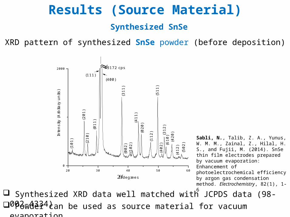
Results (Source Material) Synthesized SnSe
Synthesized XRD data well matched with JCPDS data (98-002-4334) Powder can be used as source material for vacuum evaporation
XRD pattern of synthesized SnSe powder (before deposition)
20 30 40 50 600
2000
(50
2)
(41
2)
(42
0)
(61
0)(3
12
)(4
02
)(5
11
)(1
12
)(02
0)(4
11
)(1
02
)(0
02
)(3
11
)
43172 cps
(400)(111)
(01
1)
(21
0)
(20
1)
Inte
nsi
ty (
Arb
itary
un
its)
degrees
(10
1)
Sabli, N., Talib, Z. A., Yunus, W. M. M., Zainal, Z., Hilal, H. S., and Fujii, M. (2014). SnSe thin film electrodes prepared by vacuum evaporation: Enhancement of photoelectrochemical efficiency by argon gas condensation method. Electrochemistry, 82(1), 1-6

Results (Source Material)Synthesized Cu2SnSe3
Synthesized XRD data well matched with JCPDS data (98-007-7744 ) Powder can be used as source material for vacuum evaporation
XRD pattern of synthesized Cu2SnSe3 powder (before deposition)
20 40 60 800
7000
14000
(331)/(060)
-(462)/(191)/(135)/(264)
---
-
-
-
Inte
nsi
ty (
Arb
itary
un
its)
2degrees)
(002)/(131)
(260)/(402)
(262)/(404)
-

Results (Source Material)Synthesized Cu2ZnSnSe4
Synthesized XRD data well matched with JCPDS data (98-006-7242) Powder can be used as source material for vacuum evaporation
XRD pattern of synthesized Cu2ZnSnSe4 powder (before deposition)
20 40 60 800
7000
14000
(332)/(136)
Inte
nsi
ty (
Arb
itary
un
its)
2(degrees)
(112)
(220)/(024)
(132)/(116)
(040)/(008)
Sabli, N., Talib, Z. A., Yunus, M., Mahmood, W., Zainal, Z., Hilal, H. S., and Fujii, M. (2013). CuZnSnSe Thin Film Electrodes Prepared by Vacuum Evaporation: Enhancement of Surface Morphology and Photoelectrochemical Characteristics by Argon Gas. In Materials Science Forum (Vol. 756, pp. 273-280).

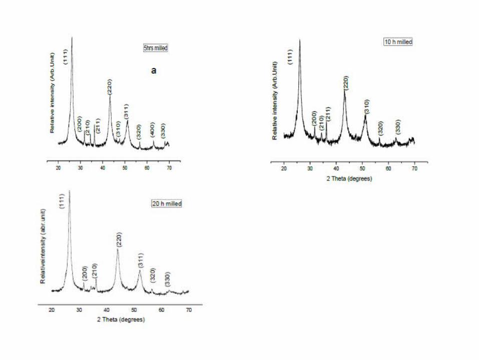
Mechanochemical solid state synthesis ofCd0.5Zn0.5Se
The starting materials were high-purity cadmium (99.99%), zinc (99.99%) and selenium (99.99%) elemental powders purchased from Alfa Aesar. Mixtures at the desired atomic ratios were placed in a stainless steel grinding jar with stainless balls under an inert atmosphere. The intensive grinding the mixtures was performed in a high-energy planetary ball mill PM 100 (Retsch) with a ball-to-powder ratio of 10:1. Grinding balls of 3 mm in diameter were used. The milling time was varied from 5 to 20 hours at a speed of 500 rpm. Small quantities of the as-milled powders were removed from the grinding jar at various time intervals for microstructural and optical characterization.


Pellet Sample Preparation
The synthesized CuSe and Cu2SnSe3 powders were weighed in the desired amount and then placed into the 8mm diameter mould to form a pellet shape sample by using a hydraulic press (SPECAC USA, model 15011) of 3 ton pressure.
The pelletization process is to force the particles into close proximity.
38mm
30mm
38mm
4.5mm
5mm
6mm
8mm 30mm
8mm
8mm
Pellet mould with 8 mm diameter
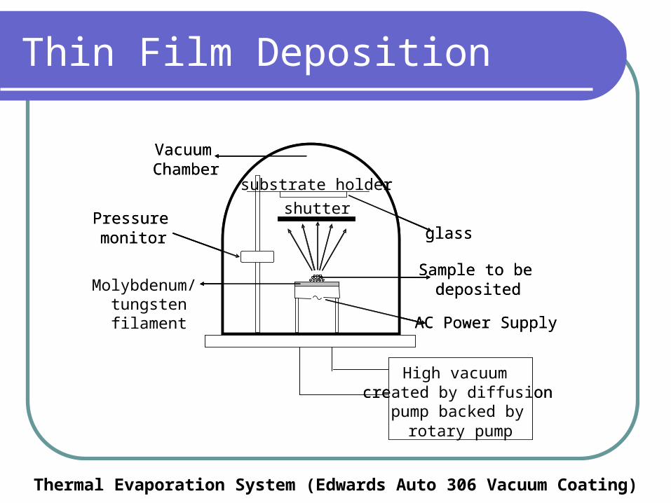
Thin Film Deposition
Vacuum Chamber
Pressure monitor
AC Power Supply
shutter
substrate holder
glass
Sample to be deposited
High vacuum created by diffusion
pump backed by rotary pump
Vacuum Chamber
Pressure monitor
AC Power Supply
shutter
substrate holder
glass
Sample to be depositedMolybdenum/
tungstenfilament
High vacuum created by diffusion
pump backed by rotary pump
Thermal Evaporation System (Edwards Auto 306 Vacuum Coating)

Methodology
Install argon gas supply & nozzle to flow argon
needlevalve
valve
Argon gas cylinder
moisture trap
Heater (setting with thermocouple to note the temperature)
Substrate (1.5cm X 2.5cm, ITO/glass)
Copper rod
Boat (Molybdenum/ tungsten)
Electrodes (Copper):connected to high current, low voltage
Sonic nozzle ( jet dia. 0.5mm)
14 cm
To diffusion pump system
Chamber pressure gauge

Hypothesis 1
Higher argon gas volume(1) Compound (atoms/ions) heats at same temp;atoms have same mean kinetic energy (Ek = 3/2 kT)
Cu (Atomic weight: 63.546)
Zn (Atomic weight : 65.409)
Sn (Atomic weight : 118.71)
Se (Atomic weight : 78.96)
(2) Lighter atoms (Cu, Zn) have higher speed due to Ek = 1/2 mV2; Higher speed more collisions with Ar atoms lose kinetic energy
(3) Higher retained kinetic energy Sn and Se are expected to react
Ar ; inert gas
Before collision
After collision
After collision
Hypothesis 2
Compound: SnSe (50:50) Compound Cu2ZnSnSe4: (25:12.5:12.5:50)
VB
CBe-
VB
CBe-
Impurity level
e-
Pure SnSe thin film (Cu,Zn): SnSe More carriers
Propose: Argon gas injection system

Annealing process
For the heat treatment process, the CuSe and Cu2SnSe3 film were placed on the quartz boat and heated with gas N2 (1cc/min) by using furnace.
The annealing process was carried out at a temperature raised from room temperature 26 oC to 100 oC, 200 oC, 300 oC, 400 oC at an increasing rate (2 oC/min).
Upon reaching the required temperature, it was maintained for 3 hours.
The temperature was then natural cooling to room temperature for 24 hours.

Methodology
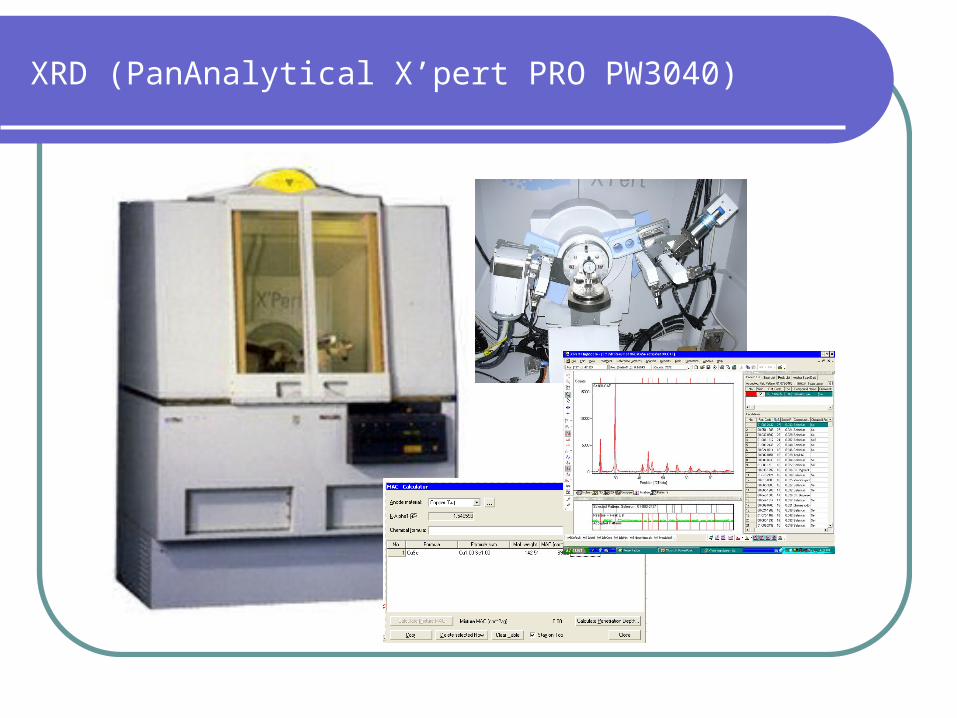
XRD (PanAnalytical X’pert PRO PW3040)

FESEM, EDX and TEM
Field Emission Scanning Electron Microscope
(JOEL JSM-6700F)
Transmission Electron
Microscope(Hitachi H7100
TEM)
Energy Dispersive X-Ray (EDX)(LEO 1455 VP SEM )

Liquid nitrogen
Argongas
vacuum
Temperature controller
Argon gasRotary pump
Two probe system
Voltmeter
Current source
Variable temperature optical cryostat
Schematic Diagram for Low Temperature Two Probe Measurement System

Liquid nitrogen
Argon gasvacuum
Temperature controller
argon gas
rotary pump
Variable temperature optical cryostat
Preamplifier
Ref SignalOscilloscope
photodiode
Camera flash
Thermocouple
sample
Schematic Diagram for Low Temperature Photoflash Technique
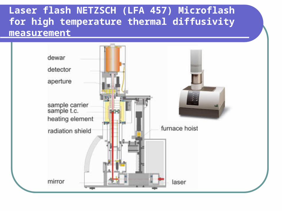
Laser flash NETZSCH (LFA 457) Microflash for high temperature thermal diffusivity measurement

Microstructure Analysis using AFM (Quesant Q-Scope 250)
The characterization of surface morphology of the CuSe thin films was studied by atomic force microscopy (AFM) technique (Quesant Q-Scope 250) in tapping mode at ambient temperature.

Ellipsometer Technique (ELX-02C)
Ellipsometer measures the change of polarization upon reflection or transmission. The ellipsometer mechanics consists of a transmitter unit (He-Ne laser – 632.8 nm) and a
receiver unit (polarising prism) fixed at the end of adjustable arms. Ellipsometry is an indirect method, i.e. in general the measured Ψ and Δ cannot be converted
directly into the optical constants of the sample, a model analysis must be performed. Using an iterative procedure (least-squares minimization) unknown optical constants and/or
thickness parameters are varied, and Ψ and Δ values are calculated using the Fresnel equations.
The calculated Ψ and Δ values, which match the experimental data best, provide the optical constants and thickness parameters of the sample

Fiber Optic Spectrophotometer
The optical studies of CuSe film analyzed using Ocean Fiber Optics Spectrophotometer.
The transmittance spectra in the region 300nnm – 800nm has been collected and optical parameters such as optical absorption coefficient and optical band gap has been evaluated.

Structural Analysis
X-Ray Powder Diffraction

20 25 30 35 40 45 50 55 60
300K
275K
250K
225K
200K
175K
150K
125K
Inte
nsi
ty (
Arb
. Un
it)
Position (2 Theta)
100K
106 11
620
210811
0
00610
210
110
0
In-situ XRD pattern of synthesized CuSe powder at 100 – 300 K
The structure was stable at the temperature range 100K – 398 K where no additional or unassigned peaks are observed

20 25 30 35 40 45 50 55 60
Pt / CuSe
323K
298K
Inte
nsity
(A
rb. U
nit)
Posistion (2 Theta)
473K
448K
423K
398K
373K
348K
Cu2Se
106
116
20210
8
110
006
102
101
100
At temperature started from 423 K, an additional peak is observed at 2 = 45.38 which corresponding to d-spacing value of 1.99 Å. This peak was identified to the standard pattern of stoichiometric Cu2Se called bellidoite (JCPDS 29-0575).
In-situ XRD pattern of synthesized CuSe powder at 298 – 473 K.

300 400 500 600 700 800 900 1000 1100 1200
65
70
75
80
85
90
95
100
105
TG DTG
Temperature, T (K)
wei
ght l
oss,
(%
)
700 K
548 K
-0.045
-0.040
-0.035
-0.030
-0.025
-0.020
-0.015
-0.010
-0.005
0.000
0.005
Der
ivat
ive
wei
ght l
oss,
dm
/dt (
%/m
in)
657 K
465 K324 K
TGA and DTG curve for synthesized CuSe powder at heating rate 10 K/min
the decomposition behaviour is attributed to the formation of
Cu2Se products due to the release of elemental Se.
20 25 30 35 40 45 50 55 60
0
5000
10000
15000
20000
25000
311
220
200
111
Cu2Se (JCPDS File No. 03-065-2982)
Inte
nsi
ty (
Arb
. Un
it)
Posistion (2 )
106 11
620
2108
110
006
102
101
100
CuSe (JCPDS File No. 34-0171)
Phase transformation from CuSe to Cu2Se structure as the synthesized
CuSe powder annealed at 653 K in N2 for 12 hours
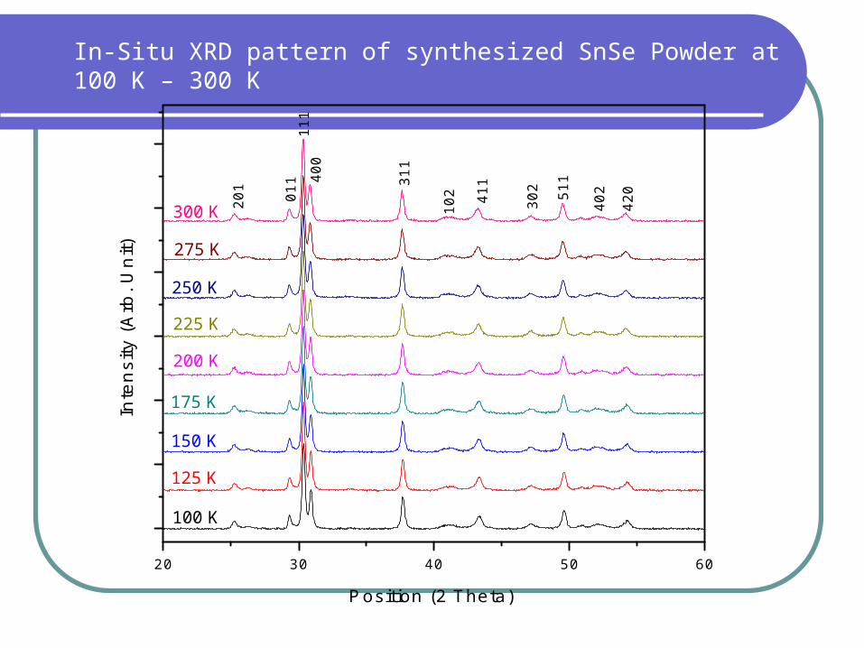
In-Situ XRD pattern of synthesized SnSe Powder at 100 K – 300 K
20 30 40 50 60
Inte
nsi
ty (
Arb
. Uni
t)
Position (2 Theta)
300 K
275 K
250 K
225 K
200 K
175 K
150 K
125 K
100 K
420
40251
1
302
411
102
311
400
111
011
201

In-Situ XRD pattern of synthesized SnSe Powder at 298 K – 473 K
20 30 40 50 60
Pt
Pt
Inte
nsi
ty (
Arb
. Un
it)
Position (2Theta)
323K
298K
473K
448K
423K
398K
373K
348K
420
402511
302
411
10231
1
400
111
011
201
The structure was stable from low temperature 100K until high temperature 473 K where no additional or unassigned peaks are observed.
This indicates that the sample powder is stable and contains no impurities.

20 30 40 50 60
0
10000
20000
30000
40000
50000
60000
70000(c)
(b)
SnSe powder (JCPDS: 48-1224)
SnSe powder annealed at 873 K (JCPDS: 48-1224)
002
22021
1
11120010
1
110
SnSnSn
502
610
501
400
Inte
nsity
(A
rb. U
nits
)
Position (2 Theta)
210
601
420
511
302
411
10231
1
111
011
201
210
221
420
402
511
302
411
10231
1
400
111
011
201
SnO2
Sn
SnSe powder annealed at 1173 K (JCPDS: 01-077-03448)
(a)
Annealing at 1173 K destroys the SnSe lattice (peaks of SnSe disappear in the sample) and leads to formation of SnO2 and Sn phases in the presence of oxygen and release of free selenium followed the reaction in eq. (5.9) [56, 57]:
2SnSe + 3O2 = SnO2 + Sn + 2SeO2

In-Situ XRD pattern of synthesized Cu2SnSe3 Powder at 100 K – 300 K.
20 30 40 50 60 70 80
300 K
275 K
250 K
225 K
200 K
175 K
150 K
125 K
Inte
nsi
ty (
Arb
. Uni
ts)
Position 2
100 K
331
400
311
220
111

In-Situ XRD pattern of synthesized Cu2SnSe3 Powder at 298 K – 523 K.
The Cu2SnSe3
structure was very stable at the temperature range 100K – 523 K where no additional or unassigned peaks are observed
20 30 40 50 60 70 80
* Pt
*
Inte
nsi
ty (
Arb
. Un
its)
Position 2
523 K
498 K
473 K
448 K
423 K
398 K
373 K
348 K
323 K
298 K
* 331
400
311
220
111

20 30 40 50 60 70 80
0
1000
2000
3000
4000
5000
6000
7000
8000
9000
10000
11000
(b)
331
40031
1
220
111
Cu2SnSe
3 powder
Sn 2O
3
Sn 2O
3
200
Cu 3S
e 2
Cu 3S
e 2
Cu 2O
Cu 2O
Cu 2O
Cu2SnSe
3 powder annealed at 753 K
Inte
nsi
ty (
Arb
. Un
its)
Position (2 Theta)
Cu 2O
331
40031
1
220
111
(a)
Comparison between the as-synthesized Cu2SnSe3 powder with the annealed
Cu2SnSe3 powder
some additional characteristic peaks attributed to the Cu3Se2 (JCPDS: 03-065-1656), Cu2O (JCPDS: 01-077-0199) and Sn2O3 (JCPDS: 25-1259) phase are observed after the Cu2SnSe3 powder annealed at 773 K.
Additional peaks present in Figure 5.35 are caused by the recrystallization and oxidation of the material at higher annealing temperature [58].

Morphology

SEM result for Synthesized CuSe powder
(a)
(b)
(c)
(d)
Fig (a-d) shows the SEM micrograph of the CuSe powder at 50000 ×, 20000 ×, 10000 × and 2500 magnification which showed particles rod-like shape.
It is observed that the smallest grain size is of the order of 37 nm.
The big islands are formed by the agglomeration of smaller grains with length in the range of 40 - 240 nm.

10-20 20-30 30-40 40-50 50-60 60-100 100-200 200-300
0
10
20
30
40
50
60
No.
of c
ount
s
Diameter size range (nm)
FESEM image and particle size distribution histogram of synthesized CuSe powder.
10-20 20-30 30-40 40-50 50-60 60-700
5
10
15
20
No
. of c
ou
nts
Diameter size range (nm)
TEM image and particle size distribution histogram of synthesized CuSe powder
• Rod like shape particles• highest count of diameter
size range in 30-40 nm range
• average diameter size distribution of 54.1 nm
• rod-like shape particles• highest count of
diameter size range in 30-40 nm
• average size distribution of 35.2 nm.
50 100 150 200 250 300 350 400 450 50020
30
40
50
60
70
80
90
Lg
D
Temperature, T (K)
Mea
n C
ryst
allit
e S
ize,
Lg (
nm)
-2.0
0.0
2.0
4.0
6.0
8.0
10.0
12.0
Dislocation D
ensityD x 10
14 (lines/m
2)
mean crystallite size obtained from XRD at temperature range of
100 – 473 K
(a)
(b)
(c)
(d)
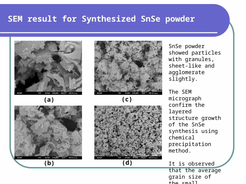
SnSe powder showed particles with granules, sheet-like and agglomerate slightly.
The SEM micrograph confirm the layered structure growth of the SnSe synthesis using chemical precipitation method.
It is observed that the average grain size of the small spherical grains is 29.14 nm.
SEM result for Synthesized SnSe powder

20-30 30-40 40-50 50-60 60-70 70-80 80-900
5
10
15
20
25
30
35
No
. of c
ou
nts
Diameter size range (nm)
FESEM image and particle size distribution histogram of synthesized SnSe powder
10-20 20-30 30-40 40-50 50-60 60-70 70-80 80-90 90-100
0
2
4
6
8
10
12
14
No.
of c
ount
s
Diameter size range (nm)
TEM image and particle size distribution histogram of synthesized SnSe powder
• flake-like or plate-like structure is built up by the interconnected network or overlapping of nanorod of the SnSe particles which agglomerates together and link to layered semiconductor.
• the highest count of diameter size is in 40-50 nm range
• average diameter size distribution of (50.6 1.2) nm.
• dispersion leads to the breakup of the flake-like or layered-like structure network into individual nanorod particles.
• highest count of particle size range in 40-50 nm
• average size distribution of (48.5 2.8) nm
100 200 300 400 500 60034
36
38
40
42
44
46
48
Mea
n cr
ysta
llit
e si
ze, L
g (nm
)
Temperature, T (K)

SEM results for synthesized Cu2SnSe3 powder
(a)
(b)
(c)
(d)
Fig. (a-d) shows the SEM micrograph of the Cu2SnSe3 powder at 50000 ×, 20000 ×, 10000 × and 2500 magnification which show particles with granules like shape.
It is observed that the average grain size of the small spherical grains is 36 nm.
The grains are well defined, spherical, of almost similar size, which indicates that the powder produced from the precipitation technique was homogenous and uniform.

100 200 300 400 500 60010
15
20
25
30
35
40
Lg
D
Temperature, T (K)
Mea
n C
ryst
allit
e S
ize,
Lg (
nm)
0.0
0.5
1.0
1.5
2.0
2.5
3.0
Dislocation D
ensity, D x 10
15 (lines/m2)
20-30 30-40 40-50 50-60 60-700
20
40
60
80
100
No
. of c
ou
nts
Diameter size range (nm)
FESEM image and particle size distribution histogram of synthesized Cu2SnSe3 powder
0-10 10-20 20-30 30-40 40-50 50-600
5
10
15
20
25
30
35
40
No
. of c
ou
nts
Diameter size range (nm)
TEM image and (b) particle size distribution histogram of synthesized Cu2SnSe3 powder
• powder is homogeneous, spherical in shape and slightly agglomerate.
• the highest count of diameter size range as (30 -40) nm
• average diameter size distributions as 36.3 nm.
• homogeneous distribution of the small spherical nanoparticles
• The highest count of diameter size range is obtained to be in between 20-30 nm
• the average size distribution being of 23.0 nm.

Electrical Properties

50 100 150 200 250 300 350 400 450 500800
850
900
950
1000
1050
region II
Ele
ctri
cal c
ondu
ctiv
ity,
(
S/cm
)
Temperature, T (K)
region I
Electrical conductivity as a function of temperature for CuSe in bulk form
variable range
hopping thermionic emission
reduction in Hall mobility
due to phonon
scattering
• the decrease of electrical conductivity can be explained by the reduction in Hall mobility, due to the influence of impurity, defect scattering, lattice scattering or surface scattering [10, 59 – 61].
• the increase of the electrical conductivity with the temperature can be explained as a consequent of thermal activation of the electrons which gained enough energy to jump across the depletion layers at the crystallite boundaries which act as potential barriers for conduction electrons [62, 63].

Hall mobility and carrier sheet densities as a function of temperature for CuSe in bulk form
• The Hall mobility of the CuSe pellet decreases from (92.9 0.9) to (5.61 0.06) cm2/Vs as the temperature increased from 100 to 300 K
• The impurities or defects inside the polycrystalline compound will develop space charge polarization with the large concentration of the charge carrier and subsequently induced trapping or localization process which decrease the electrical conductivity [64].
• the carrier sheet density of the CuSe pellet increase from (2.54 0.03) 1019 to (3.08 0.03) 1019 cm-2 with increasing temperature which corresponds to the behaviour normally observed in a non-degenerate semiconductor trend.
• This behaviour can be explained by the usual impurity concentration in which the excitation of conduction electrons occurs from impurity centres [65].
100 150 200 250 300
10
100 N
c
Temperature, T (K)
Hal
l mob
ilit
y,
H (
cm2 /
Vs)
T-2.52
1E19
1E20
1E21
Car
rier
she
et d
ensi
ty, N
c (cm
-2)

• The temperature dependence of the conductivity in the higher temperature range (349- 449 K) follows the thermionic emissions over the grain boundary potential model and obeys Seto’s [66, 67] extended version of the Petritz model using equation:
• The linearity of the plots reveals that thermally-assisted thermionic emission over the grain boundary potential contributes to the conduction mechanism and the grain boundary scattering of charge carriers is more predominant in the samples investigated.
• It is believed that the small value of activation energy in the this temperature region is the energy required to overcome the grain boundary potential in this polycrystalline materials
Thermionic Emission
2.2 2.3 2.4 2.5 2.6 2.7 2.8 2.99.60
9.65
9.70
9.75
9.80
9.85
9.90
9.95
10.00
ln (T
1/2 )
1000/T
Ea = (46 4) meV
kT
EexpT a
o
ln (T1/2) versus (1000/T) at 349- 449 K for CuSe in bulk form

Variable Range Hopping
0.26 0.27 0.28 0.29 0.30 0.31 0.329.20
9.25
9.30
9.35
9.40
9.45
ln (T
1/2 )
T-1/4 (K-1/4)
ln (T1/2) versus (T-1/4) at 99 - 214 K for CuSe in bulk form
The hopping conduction mechanism should dominate at low temperatures since the electrons do not have sufficient energy to cross the potential barrier through thermionic emission.According to Mott, variable range hopping is expected to be predominant at the lowest temperature as electron can hops to the nearest neighbouring empty site or move to a more energetically similar remote site and leads to conductivity–temperature dependence follows equation [68, 69]:
the linear variation observed between 99 – 214 K with a good fit to the conductivity–temperature data indicates that the possible conduction mechanism at these temperatures can be described by Mott’s [67, 70] variable range hopping law.
4/1
oho T
TexpT

100 200 300 400 500 600
0.0
0.5
1.0
1.5
2.0
2.5
Ele
ctri
cal c
ondu
ctiv
ity,
(
S/c
m)
Temperature, T (K)
Electrical conductivity as a function of temperature for SnSe in bulk form
thermionic emission
variable range
hopping
• The electrical conductivity is found to increase slowly in the temperature range 100 K-396 K followed by a drastically increase above 420 K.
• The nature of response exhibits the ordinary semiconducting behaviour of the material throughout the temperature range.
• The substantial increase in electrical conductivity of the SnSe pellet is mainly determined by the carrier sheet density of the sample which depict the carrier sheet density of the SnSe pellet follows an exponential temperature dependence of a typical semiconductors.

100 150 200 250 3000.1
1
10
100
1000
10000
100000
H
Nc
Temperature, T (K)
Ha
ll m
ob
ility
, H (
cm2 /
Vs)
1E9
1E10
1E11
1E12
1E13
1E14
1E15
Ca
rrie
r S
he
et D
en
sity
, Nc (
cm-2)
T-7.15
Hall mobility and carrier sheet densities as a function of temperature for SnSe in bulk form
• the mobility decreases as the temperature increased from 100 to 300 K.
• In polycrystalline semiconductors the transport of carrier is driven by scattering mechanism at intercrystallite boundaries, rather than by intracrystallite characteristics.
• Based on the grain boundary trapping theory, the decrease of mobility and steep rise of the carrier is due to the total carrier depletion of the grains which able to capture and therefore immobilize free carriers [71, 72].

1.9 2.0 2.1 2.2 2.3 2.4 2.5 2.60.5
1.0
1.5
2.0
2.5
3.0
3.5
4.0
ln (T
)1/2
1000/T
Ea = (0.44 0.03) eV
ln (T1/2) versus (1000/T) at 396- 526 K for SnSe in bulk form.
• The variation of ln (T1/2) with inverse temperature is found to be fit linearly in the temperature range from 396 to 526 K for the SnSe pellet indicating that the conduction in this system is through the thermally assisted thermionic emissions over the grain boundary potential model [66, 67].
• Conductivity in SnSe pellet increases exponentially with temperature indicating the heat induced energy which overcome the barrier at the grain boundaries within the sample.
Thermionic Emission

Variable Range Hopping
0.25 0.26 0.27 0.28 0.29 0.30 0.31-4.0
-3.5
-3.0
-2.5
-2.0
-1.5
-1.0
-0.5
0.0
0.5
ln (T
)1/2
T-1/4 (K-1/4)
ln (T1/2) versus (T-1/4) at 113 – 243 K for SnSe in bulk form
• The linear dependence of the ln (T1/2) vs. T-1/4 can be interpreted as hopping transport phenomena.
• The possible conduction mechanism at these temperatures ranges may be due to a wide range of localization and variable range hopping conduction in the localized states [67, 70].
• At lower temperature, the localized states conduction gradually becoming predominant due to the fact that the probably of thermal release of the carriers from the localized states near the mobility edge becomes rapidly smaller and charge carrier is more likely to hop to a neighbor site in the distribution [73].

100 200 300 400 500 600
500
550
600
650
700
750
region II
region I
Ele
ctri
cal c
ondu
ctiv
ity,
(
S/cm
)
Temperature, T(K)
Electrical conductivity as a function of temperature for Cu2SnSe3 in bulk form
• A decrease in conductivity observed for the Cu2SnSe3 pellet in region I (99 – 375 K) follow the Hall mobility results closely
• The increase of the electrical conductivity in region II indicates the carriers within these polycrystalline material obtain sufficient energy to cross the potential barriers at the grain boundaries.
• The increase of carrier sheet density resulted from the reduction of the intergrain barriers above 375 K also increase the conductivity [72].
reduction in Hall mobility due to
phonon scattering
variable range
hopping thermionic emission

100 150 200 250 300
1
2
3
N
c
Temperature, T (K)
Hal
l mob
ilit
y, H
(cm
2 /Vs)
T-0.72
T-2.05
5E19
1E20
1.5E20
2E20
2.5E20
Car
rier
she
et d
ensi
ty, N
c (cm
-2)
Hall mobility and carrier sheet densities as a function of temperature for Cu2SnSe3 in bulk
form
• The Hall mobility of the Cu2SnSe3
compound decreases as the temperature increases from 100 to 300 K attributed to the increased scattering due to the influence of impurity, defect scattering, lattice scattering, neutral or ionized impurity scattering and grain boundary scattering or surface scattering [10, 59 – 61, 74, 75].
• The temperature dependence of Hall mobility fit the classical scattering mechanism at region I indicating that acoustic lattice scattering is a dominant effect in the carrier transport from 125 to 200 K.
• At region II, it is believed that the presence of grain boundaries in polycrystalline material explained according to Seto’s grain boundary trapping theory will affect the results of the temperature dependence mobility for Cu2SnSe3 pellet [66].
Region I
Region II
• The carrier sheet density increases as the temperature increased from 100 to 300 K.
• At higher temperature (200 – 300 K), the increase of carrier sheet density can be explained by a usual impurity concentration in which the excitation of conduction electrons occurs from impurity centres [65].
• Further temperature decrease down to 100 K leads to an exponential decrease of the carrier sheet density due to freezing of electrons to the shallow level impurities.

Thermionic Emission
1.9 2.0 2.1 2.2 2.3 2.4 2.5 2.6 2.79.1
9.2
9.3
9.4
9.5
9.6
9.7
ln (T
1/2 )
1000/T
Ea = (54 3) meV
ln (T1/2) versus (1000/T) at 375- 523 K for Cu2SnSe3 in bulk form
• the variation of conductivity as a function of temperature in higher temperature range (375 – 523 K) is explained by the polycrystalline nature of the Cu2SnSe3 pellet with
existence of potential barriers at grain boundaries followed the model of thermionic emissions across grain boundary barrier conduction [66, 71, 76, 77].
• The conductivity of these polycrystalline Cu2SnSe3 pellet depends sensitively on the grain boundaries such as the potential barriers and space charge region that are built up around them.

Variable Range Hopping
0.23 0.24 0.25 0.26 0.27 0.28 0.29
8.95
9.00
9.05
9.10
9.15
9.20
ln (T
1/2 )
T-1/4 (K-1/4)
• The ln (T1/2) vs. T-1/4 plots in Figure fit linear for the temperature range of (148 - 328 K) which obeys the Mott’s T-1/4 law propose the occurrence of variable range hopping conduction as the most suitable conduction mechanism for explaining the conduction process in this temperature range.
• In the hopping conduction, electron can hops to the nearest neighbouring empty site or move to a more energetically similar remote site according to Mott [78].
ln (T1/2) versus (T-1/4) at 148 – 328 K for Cu2SnSe3 in bulk form

Thermal Properties

50 100 150 200 250 300 350 400 450 5000.005
0.006
0.007
0.008
0.009
0.010
0.011
0.012
0.013
1/
Temperature, T (K)
The
rmal
Diff
usiv
ity,
(cm
2/s
)
80
100
120
140
160
180
1/ (s/cm
2)
Thermal diffusivity and reciprocal thermal diffusivity measurement as a function of
temperature on CuSe pellet
• Thermal diffusivity decreased from 1.20 10-2 to 6.01 10-3 cm2/s as temperature increased from 100 to 473 K.
• increase of phonon scattering (as phonons pass through the sample, they are scattered by the heavier atom which contributed by the carriers in the compound, grain boundaries as well as other phonons)
• decrease in the mobility of free charge carrier as shown in Hall mobility results
• Phonon scattering can be separate into temperature dependent intrinsic scattering factor and temperature independent extrinsic scattering factor
lattice heat transfer (intrinsic scattering) is dominant in
100 – 350 K

50 100 150 200 250 300 350 400 450 500 550
0.0015
0.0020
0.0025
0.0030
0.0035
0.0040
region IIIregion II
1/
Temperature, T (K)
Th
erm
al D
iffu
sivi
ty,
(cm
2/s
)
region I
250
300
350
400
450
500
550
600
650
1/
(s/cm2)
• thermal diffusivity results decrease from 3.80 10 -3 to 1.60 10 -3 cm2/s as the temperature increased from 100 to 523 K
• increase of phonon scattering (as phonons pass through the sample, they are scattered by the heavier atom which contributed by the carriers in the compound, grain boundaries as well as other phonons)
• decrease in the mobility of free charge carrier as shown in Hall mobility results (scattering process and phonon collisions decrease the mobility of charge carriers and subsequently decrease the thermal diffusivity)
• Phonon scattering can be separate into temperature dependent intrinsic scattering factor and temperature independent extrinsic scattering factor
lattice heat transfer may be dominant in this three temperature
range
Thermal diffusivity and reciprocal thermal diffusivity measurement as a
function of temperature on SnSe pellet

50 100 150 200 250 300 350 400 450 500 550 6000.0028
0.0030
0.0032
0.0034
0.0036
0.0038
0.0040
0.0042
0.0044
region II
1/
Temperature, T (K)
Th
erm
al D
iffu
sivi
ty,
(cm
2/s
)
region I
220
240
260
280
300
320
340
1/
(s/cm2)
Thermal diffusivity and reciprocal thermal diffusivity measurement as a function of
temperature on Cu2SnSe3 pellet
• the thermal diffusivity value decreases from 4.18 10-3 to 2.97 10-3 cm2/s when the temperature increased from 100 to 523 K.
• increase of phonon scattering (as phonons pass through the sample, they are scattered by the heavier atom which contributed by the carriers in the compound, grain boundaries as well as other phonons)
• decrease in the mobility of free charge carrier as shown in Hall mobility results (scattering process and phonon collisions decrease the mobility of charge carriers and subsequently decrease the thermal diffusivity)
lattice heat transfer may be dominant in this three temperature range

Effect of annealing process
CuSe film
250 300 350 400 450 500 550 600 650 700
2500
3000
3500
4000
4500
5000
5500
6000
6500
Ele
ctri
cal C
on
du
ctiv
ity, (S
/cm
)
Annealing Temperature (K)250 300 350 400 450 500 550 600 650 700
2.00
2.10
2.20
2.30
2.40
2.50
2.60
2.70
Eopt
nr
Annealing Temperature, T (K)
Opt
ical
Ban
d G
ap, E
op
t (eV
)
3.200
3.220
3.240
3.260
3.280
3.300
3.320
3.340
Refractive Indices, n
r
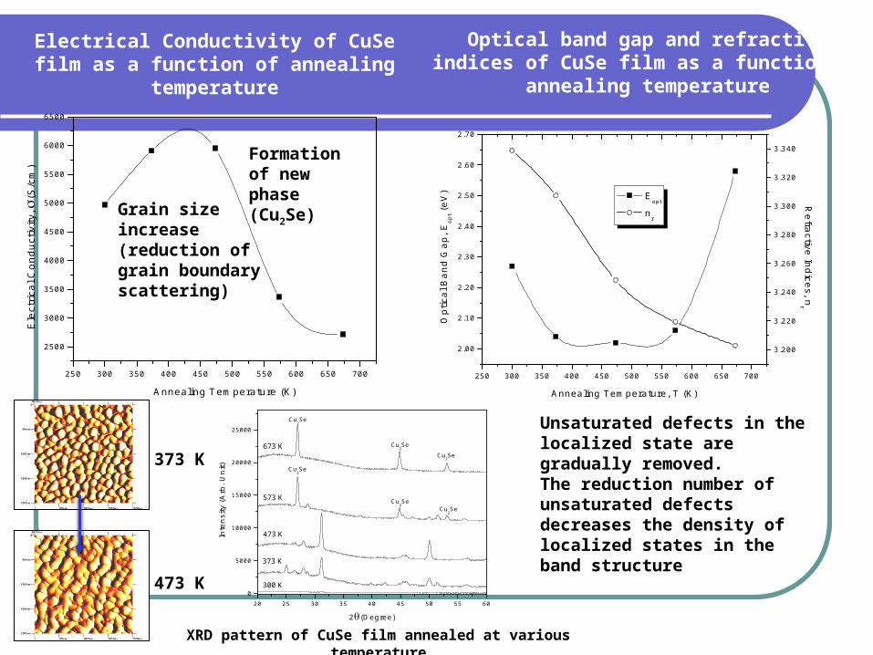
Grain size increase (reduction of grain boundary scattering)
Formation of new phase (Cu2Se)
Unsaturated defects in the localized state are gradually removed. The reduction number of unsaturated defects decreases the density of localized states in the band structure
20 25 30 35 40 45 50 55 60
0
5000
10000
15000
20000
25000
Cu2Se
Cu2Se
Cu2Se
Cu2Se
Cu2Se
Inte
nsi
ty (
Arb
. Uni
t)
2(Degree)
673 K
573 K
473 K
373 K
300 K
Cu2Se
373 K
473 K
XRD pattern of CuSe film annealed at various temperature
Electrical Conductivity of CuSe film as a function of annealing temperature
Optical band gap and refractive indices of CuSe film as a function of annealing
temperature

Effect of annealing process
SnSe Thin Film

decrease in grain size
• formation of new phase
• (SnO2)• grain growth
drastically
373 K 473 KAs-deposited
573 K 673 K
250 300 350 400 450 500 550 600 650 700
0.00
0.02
0.04
0.06
0.08
0.10
0.12
Ele
ctri
cal C
on
du
ctiv
ity,
(S/c
m)
Annealing Temperature, T (K)
20 25 30 35 40 45 50 55 600
2000
4000
6000
8000
10000
12000
14000
SnO2
SnO2
SnO2SnO
2
SnO2
373 K
473 K
573 K
673 K
Inte
nsi
ty (
Arb
. Un
it)Position (2 Theta)
300 K
SnO2
SnO
AFM images
Electrical Conductivity of SnSe film as a function of annealing temperature
XRD pattern of SnSe films annealed at various temperature

During annealing, unsaturated defects in the localized state are gradually removed. The reduction number of unsaturated defects decreases the density of localized states in the band structure and consequently decreased the the nr
250 300 350 400 450 500 550 600 650 7000.8
1.0
1.2
1.4
1.6
1.8
2.0
2.2
2.4
2.6
2.8
Eopt, indirect
Eopt, direct
n
Annealing Temperature, T (K)
Op
tica
l Ba
nd
Ga
p, E
op
t (e
V)
1.000
1.050
1.100
1.150
1.200
1.250
1.300
1.350
Re
fractive
Ind
ices, n
r
Optical band gap and refractive indices of SnSe film as a function of annealing
temperature
This behaviour may be attributed to the removal of water vapour or defect level
from the SnSe film after annealing process .
Eopt for the annealed SnSe film is obtained based on the direct allowed transition mechanism. sharp change of Eopt may be connected to partial convertion of tin selenide film to tin oxide film
20 25 30 35 40 45 50 55 600
2000
4000
6000
8000
10000
12000
14000
SnO2
SnO2
SnO2SnO
2
SnO2
373 K
473 K
573 K
673 K
Inte
nsi
ty (
Arb
. Uni
t)
Position (2 Theta)
300 K
SnO2
SnO

Effect of annealing process
Cu2SnSe3 Thin Film

increase in grain size
improvement of crystallinity
373 K 473 KAs-deposited
573 K 673 K
AFM images20 25 30 35 40 45 50 55 60
0
500
1000
1500
2000
2500
673 K
573 K
473 K
373 K
311
220
Inte
nsi
ty (
Arb
. Un
it)Position (2 Theta)
300 K
111
XRD pattern of Cu2SnSe3 film annealed at various temperature
250 300 350 400 450 500 550 600 650 7002000
2500
3000
3500
4000
4500
Ele
ctri
cal C
on
du
ctiv
ity,
(S
/cm
)
Annealing Temperature, T (K)
Electrical Conductivity of Cu2SnSe3 film as a function of annealing
temperature

During annealing, unsaturated defects in the localized state are gradually removed. The reduction number of unsaturated defects decreases the density of localized states in the band structure and consequently decreased the the nr The increase of surface roughness at the Cu2SnSe3 films interface contributed to the increased surface optical scattering and optical loss which might lead to decrease of the n r
250 300 350 400 450 500 550 600 650 7002.22
2.24
2.26
2.28
2.30
2.32
2.34
2.36
2.38
2.40
Eopt, direct
n
Annealing Temperature, T (K)
Op
tica
l Ba
nd
ga
p, E
op
t (e
V)
1.400
1.500
1.600
1.700
1.800
1.900
2.000
2.100
2.200
Re
fractive
Ind
ices, n
r
Optical band gap and refractive indices of Cu2SnSe3 film as a function of annealing
temperature
the change of the average grains into
effectively larger grains

REFERENCES
1. Loferski, J.J. J. Appl. Phys., 1956. 27(7): 777-784.
2. Kainthla, R.C., Pandya, D.K., Chopra, K.L. J. Electrochem. Soc., 1982. 129(1): 99-102.
3. Lakshmikumar, S.T., Rastogi, A.C. Sol. Energy Mater. Sol. Cells, 1994. 32(1): 7-19.
4. Grozdanov, I. Synth. Met., 1994. 63(3): 213-216.
5. Li, B., Xie, Y., Huang, J., Qian, Y. Ultrason. Sonochem., 1999. 6(4): 217-220.
6. Bhuse, V.M., Hankare, P.P., Garadkar, K.M., Khomane, A.S. Mater. Chem. Phys., 2003. 80(1): 82-88.
7. Dhanam, M., Manoj, P.K., Prabhu, R.R. J. Cryst. Growth, 2005. 280(3-4): 425-435.
8. Zhang, S.Y., Fang, C.X., Tian, Y.P., Zhu, K.R., Jin, B.K., Shen, Y.H., Yang, J.X. Cryst. Growth Des., 2006. 6(12): 2809-2813.
9. Ambade, S.B., Mane, R.S., Kale, S.S., Sonawane, S.H., Shaikh, A.V., Han, S.-H. Appl. Surf. Sci., 2006. 253(4): 2123-2126.
10. Seoudi, R., Shabaka, A.A., Elokr, M.M., Sobhi, A. Mater. Lett., 2007. 61(16): 3451-3455.
11. Gosavi, S.R., Deshpande, N.G., Gudage, Y.G., Sharma, R. J. Alloys Compd., 2008. 448(1-2): 344-348.
12. Hankare, P.P., Khomane, A.S., Chate, P.A., Rathod, K.C., Garadkar, K.M. J. Alloys Compd., 2009. 469(1-2): 478-482.
13. Hermann, A.M., Fabick, L. J. Cryst. Growth, 1983. 61(3): 658-664.
14. Chu, T.L., Chu, S.S., Lin, S.C., Yue, J. J. Electrochem. Soc., 1984. 131(9): 2182-2185.
15. O'Brien, R.N., Santhanam, K.S.V. J. Electrochem. Soc., 1992. 139(2): 434-437.
16. Bhattacharya, R.N., Fernandez, A.M., Contreras, M.A., Keane, J., Tennant, A.L., Ramanathan, K., Tuttle, J.R., Noufi, R.N., Hermann, A.M. J. Electrochem. Soc., 1996. 143(3): 854-858.
17. Lakshmi, M., Bindu, K., Bini, S., Vijayakumar, K.P., Kartha, C.S., Abe, T., Kashiwaba, Y. Thin Solid Films, 2001. 386(1): 127-132.
18. Pathan, H.M., Lokhande, C.D., Amalnerkar, D.P., Seth, T. Appl. Surf. Sci., 2003. 211(1-4): 48-56.
19. Padam, G.K. Thin Solid Films, 1987. 150(1): L89-L92.
20. Haram, S.K., Santhanam, K.S.V. Thin Solid Films, 1994. 238(1): 21-26.

21. Levy-Clement, C., Neumann-Spallart, M., Haram, S.K., Santhanam, K.S.V. Thin Solid Films, 1997. 302(1-2): 12-16.
22. Heyding, R.D., Murray, R.M. Can. J. Chem., 1976. 54(6): 841-848
23. Estrada, C.A., Nair, P.K., Nair, M.T.S., Zingaro, R.A., Meyers, E.A. J. Electrochem. Soc., 1994. 141(3): 802-806.
24. Garcia, V.M., Nair, P.K., Nair, M.T.S. J. Cryst. Growth, 1999. 203(1-2): 113-124.
25. Taylor, C.A., Underwood, F.A. Acta Crystallogr., 1960. 13(4): 361-362.
26. Elliott, J.A., Bicknell, J.A., Collinge, R.G. Acta Crystallogr., Sect. B: Struct. Crystallogr. Cryst. Chem., 1969. 25(11): 2420
27. Al-Mamun, Islam, A.B.M.O. Int. J. Mod. Phys. B, 2004. 18(22): 3063-3069.
28. Agarwal, A., Patel, P.D., Lakshminarayana, D. J. Cryst. Growth, 1994. 142(3-4): 344-348.
29. Chun, D., Walser, R.M., Bene, R.W., Courtney, T.H. Appl. Phys. Lett., 1974. 24(10): 479-481
30. Baxter, C.R., McLennan, W.D. J. Vac. Sci. Technol., A, 1975. 12(1): 110-113.
31. Valiukonis, G., Guseinova, D.A., Keivaitb, G., Sileika, A. Phys. Status Solidi B, 1986. 135(1): 299-307.
32. Ganesan, N., Sivaramakrishnan, V. Semicond. Sci. Technol., 1987. 2(8): 519.
33. Wang, L.-S., Niu, B., Lee, Y.T., Shirley, D.A., Balasubramanian, K. J. Chem. Phys., 1990. 92(2): 899-908.
34. John, K.J., Pradeep, B., Mathai, E. J. Mater. Sci., 1994. 29(6): 1581-1583.
35. Xie, Y., Su, H., Li, B., Qian, Y. Mater. Res. Bull., 2000. 35(3): 459-464.
36. Lindgren, T., Larsson, M., Lindquist, S.-E. Sol. Energy Mater. Sol. Cells, 2002. 73(4): 377-389.
37. Zainal, Z., Nagalingam, S., Kassim, A., Hussein, M.Z., Yunus, W.M.M. Sol. Energy Mater. Sol. Cells, 2004. 81(2): 261-268.
38. Agarwal, A., Chaki, S.H., Lakshminarayana, D. Mater. Lett., 2007. 61(30): 5188-5190.
39. Nabi, Z., Kellou, A., Mecabih, S., Khalfi, A., Benosman, N. Mater. Sci. Eng., B, 2003. 98(2): 104-115.
40. Quan, D.T. Thin Solid Films, 1987. 149(2): 197-203.

41. Julien, C., Eddrief, M., Samaras, I., Balkanski, M. Mater. Sci. Eng., B, 1992. 15(1): 70-72.
42. Subramanian, B., Mahalingam, T., Sanjeeviraja, C., Jayachandran, M., Chockalingam, M.J. Thin Solid Films, 1999. 357(2): 119-124.
43. Spitzer, D.P. J. Phys. Chem. Solids, 1970. 31(1): 19-40.
44. Shay, J.L., Wernick, J.H. Ternary chalcopyrite semiconductors: growth, electronic properties and applications; Pergamon: Oxford 1975.
45. Kuhs, W.F., Nitsche, R., Scheunemann, K. Mater. Res. Bull., 1979. 14(2): 241-248.
46. Samanta, L.K., Ghosh, D.K., Bhar, G.C. Phys. Status Solidi A, 1986. 93(1): K51-K54.
47. Samanta, L.K. Phys. Status Solidi A, 1987. 100(1): K93-K97.
48. Boldish, S.I., White, W.B. Am. Mineral., 1998. 83(7-8): 865-871
49. Chen, X.-a., Wada, H., Sato, A., Mieno, M. J. Solid State Chem., 1998. 139(1): 144-151.
50. Onoda, M., Chen, X.-a., Sato, A., Wada, H. Mater. Res. Bull., 2000. 35(9): 1563-1570.
51. Marcano, G., Bracho, D.B., Rincon, C., Perez, G.S., Nieves, L. J. Appl. Phys., 2000. 88(2): 822-828.
52. Skoug, E.J., Cain, J.D., Morelli, D.T. J. Alloys Compd., 2010. 506(1): 18-21.
53. Berger, L.I., Prochukhan, V.D. Ternary diamond-like semiconductors; Consultants Bureau: New York. 1969.
54. Feigelson, R. Jpn. J. Appl. Phys., 1980. 19((Supplement 19-3)): 371-376.
55. Marcano, G., Rincon, C., de Chalbaud, L.M., Bracho, D.B., Perez, G.S. J. Appl. Phys., 2001. 90(4): 1847-1853.
56. Badrinarayanan, S., Mandale, A., Gunjikar, V., Sinha, A. J. Mater. Sci., 1986. 21(9): 3333-3338.
57. Kale, R.B., Lokhande, C.D. Appl. Surf. Sci., 2005. 252(4): 929-938.
58. Kale, R.B., Lokhande, C.D. J. Phys. Chem. B, 2005. 109(43): 20288-20294.
59. Kazmerski, L.L., Berry, W.B., Allen, C.W. J. Appl. Phys., 1972. 43(8): 3515-3521.
60. Hummel, R.E. Electronic Properties of Materials; 3rd ed.; Springer-Verlag: New York. 2001.

61. Ghazanfar, U., Siddiqi, S.A., Abbas, G. Mater. Sci. Eng., B, 2005. 118(1-3): 132-134.
62. Petritz, R.L. Phys. Rev., 1956. 104(6): 1508.
63. Mahmoud, S.A., Ashour, A., Badawi, E.A. Appl. Surf. Sci., 2006. 253(5): 2969-2972.
64. Prasad, M., Pandit, A.K., Ansari, T.H., Singh, R.A. Mater. Chem. Phys., 1991. 30(1): 13-17.
65. Berger, H., Jäniche, G., Grachovskaya, N. Phys. Status Solidi B, 1969. 33(1): 417-424.
66. Seto, J.Y.W. J. Appl. Phys., 1975. 46(12): 5247-5254.
67. Thamilselvan, M., Premnazeer, K., Mangalaraj, D., Narayandass, S.K. Physica B (Amsterdam, Neth.), 2003. 337(1-4): 404-412.
68. Mott, N.F., Davis, E.A. Electronic process in non-crystalline materials; 2nd ed.; Clarendon Press: Oxford. 1979.
69. Mott, N.F. Metal-insulator transitions; Taylor & Francis: London. 1974.
70. Sharma, R.P., Shukla, A.K., Kapoor, A.K., Srivastava, R., Mathur, P.C. J. Appl. Phys., 1985. 57(6): 2026-2029.
71. Baccarani, G., Ricco, B., Spadini, G. J. Appl. Phys., 1978. 49(11): 5565-5570.
72. Bertran, E., et al. J. Phys. D: Appl. Phys., 1984. 17(8): 1679.
73. Hafiz, M.M., Othman, A.A., Elnahass, M.M., Al-Motasem, A.T. Physica B (Amsterdam, Neth.), 2007. 390(1-2): 286-292.
74. Shandalov, M., Dashevsky, Z., Golan, Y. Mater. Chem. Phys., 2008. 112(1): 132-135.
75. Ireland, J.R. Ph.D. Thesis. Transport characteristics of novel degenerate semiconductor materials - chalcogenide based thermoelectric systems and cadmium oxide based thin film transparent conducting oxide systems. Northwestern University, 2004.
76. Pike, G.E., Seager, C.H. J. Appl. Phys., 1979. 50(5): 3414-3422.
77. Bernède, J.C., Manai, N., Morsli, M., Pouzet, J., Marie, A.M. Thin Solid Films, 1992. 214(2): 200-206.
78. Yildiz, A., Alsaç, A., Serin, T., Serin, N. J. Mater. Sci.: Mater. Electron., 2010. 1-4.

ACKNOWLEDGEMENTS
The authors would like to thank the Ministry of Education and Universiti Putra Malaysia for
their financial support through (FRGS 5524428), (RUGS 9341400) and (Geran
Putra 9433966)

Thank you