universiti putra malaysia design of direct …psasir.upm.edu.my/12071/1/fk_2002_37_a.pdf · design...
TRANSCRIPT
UNIVERSITI PUTRA MALAYSIA
DESIGN OF DIRECT SEQUENCE CODE DIVISION MULTIPLE ACCESS (DS-CDMA) WIRELESS TRANSMITTER USING FIELD
PROGRAMMABLE GATE ARRAY (FPGA)
KHALID ELTAHIR MOHAMED OSMAN
FK 2002 37
DESIGN OF DIRECT SEQUENCE CODE DIVISION MULTIPLE ACCESS (DS-CDMA) WIRELESS TRANSMITTER USING FIELD
PROGRAMMABLE GATE ARRAY (FPGA)
By
KHALID ELT AHIR MOHAMED OSMAN
Thesis Submitted to the School of Graduate Studies, Universiti Putra Malaysia, In Fulfilment of the Requirement for the Degree of Master of Science
August 2002
Dedicated
To you . . . . . . Dear mother . . . . for making out of us the
person who can present such a work . . . for doing all this with pleasure . . . . . .
To you . . . . . . . Dear brother Amin . . . . the person who lead to
success life . . . and taught me how to face my struggles . . . . .
To you . . . . . . Dear brothers, sisters, nephews and niece . . .
Mohamed, Awad, Nura, Fathia, Sadia, Asma, Omima, Ahmed, Sumia, Mahmoud, Amna, Mohamed, lina, Dania . . .
To all the glory inside you . . .
To you . . . . . . love . . . thanks . . . and my simple effort . . .
11

iii
Abstract of thesis presented to the Senate of Universiti Putra Malaysia in fulfilment of the requirement for the degree of Master of Science
DESIGN OF DIRECT SEQUENCE CODE DIVISION MULTIPLE ACCESS (DS-CDMA) WIRELESS TRANSMITTER USING FIELD
PROGRAMMABLE GATE ARRAY (FPGA)
By
KHALID ELTAHIR MOHAMED OSMAN
August 2002
Chairman: Professor Borhanuddin Mohd. Ali. Ph.D.
Faculty: Engineering
This thesis describes the DS-CDMA wireless transmitter design using FPGA (Field
Programmable Gate Array), which has been adopted in many wireless access
technologies. Four separate blocks have been designed using digital approach to
form the transmitter circuit diagram using the oscillator, the PN-code generator, the
Parity Check, and the BPSK modulator. The Synopsys software has been used for
the design synthesis and simulation; the VHDL (Very High Speed Integrated Circuit
Hardware Description Language (VHDL» program was used for coding and FPGA
for compiling and downloading the simulation in FPGA cards.
The DS-CDMA wireless transmitter was designed to transmit with data rates up to 2
Mbps. The transmitted signals were carried out with a 40 MHz carrier frequency.
VHDL files were created for each element of the wireless transmitter. Each file was
simulated and synthesized using FPGA compiler II. The control block was added for
timing purposes and for framing the coded data. One bit parity was added to the data
frame containing 1 6 serial bits.
IV
The top-level design file was initiated using VHDL for the combined elements of the
DS-CDMA wireless transmitter including the control block. The results of simulated
and synthesized top-level design file using FPGA compiler II were downloaded into
the Xilinx XSV300 FPGA board.
This study has demonstrated the design of DS-CDMA wireless transmitter with
higher data rates using FPGA. It has also improved the performance and quality of
the transmitted data by including error detection and correction.
Abstrak tesis yang dikemukakan kepada Senat Universiti Putra Malaysia sebagai memenuhi keperluan untuk ijazah Master Sains
REKA BENTUK PENGHANTAR WAYARLES CAPAIAN KOD BERBILANG DIVISI-JUJUKAN TERUS (DS-CDMA) DENGAN
MENGGUNAKAN SUS UN TERTIB GET LAPANGAN BOLEH PROGRAM (FPGA)
Oleh
KHALID ELT AHIR MOHAMED OSMAN
Ogos 2002
Pengerusi Profesor Borhanuddin Mohd. Ali, Ph.D.
Fakulti Kejuruteraan
v
Projek ini menghuraikan reka bentuk penghantar wayarles capaian kod berbilang
divisi -jujukan terns (DS-CDMA) menggunakan susun tertib get lapangan boleh
program (FPGA) yang telah digunakan dalam banyak teknologi capaian wayarles.
Empat blok berasingan telah direka bentuk dengan pendekatan digit, menggunakan
oksilator, penjana kod-PN, semakan pariti dan pemodulat BPSK untuk membentuk
gambar rajah litar penghantar. Implementasi dan perisian sintesis digunakan untuk
menggabungkan keseluruhan komponen. Perisian Sinopsis digunakan untuk reka
bentuk dan simulasi. Program VHDL (Very High Speed Integrated Circuit Hardware
Description Language) digunakan untuk pengkodan, dan FPGA (Field
Programmable Gate Array) digunakan untuk kompilasi dan muat turun simulasi ke
dalam kad FPGA.
vi
Penghantar wayarles DS-CDMA direka bentuk untuk melakukan penghantaran
dengan kadar data sehingga 2Mbps. Isyarat yang dihantar dilaksanakan oleh
pembawa berfrekuensi 40 MHz.
Fail VHDL dicipta untuk setiap unsur pada penghantar wayarles. Setiap fail
disimulasi dan disintesis dengan menggunakan Pengompil II FPGA. Blok kawalan
ditambahkan bagi maksud pemasaan dan kerangkaan bagi data terkod. Satu bit pariti
ditambahkan pada kerangka data yang mengandungi 1 6 bit sesiri.
Fail reka bentuk paras tertinggi diwujudkan dengan menggunakan VDHL untuk
unsur-unsur (penghantar wayarles DS-CDMA) yang digabungkan dan termasuk blok
kawalan. Hasil reka bentuk paras terrtinggi tersimulat dan tersintesis yang
menggunakan pengompil II FPGA telah dimuat turunkan ke dalam papan FPGA
Xilina XSV300.
Kajian ini telah menunjukkan reka bentuk penghantar wayarles DS-CDMA dengan
kadar data lebih tinggi menggunakan FPGA. Kajian ini juga telah memperbaiki
pre stasi dan kualiti data yang dihantar dengan cara memasukkan pengesanan dan
pembetulan ralat . Kaedah yang disyorkan yang berasaskan pemodelan perilaku
memberi keupayaan simulasi yang unggul.
Vll
ACKNOWLEDGMENTS
Is all praIse to Almighty Allah (SWT) the most Benevolent, Merciful and
Compassionate, for giving me the utmost strength, patience and guidance to have this
work completed.
I would like to express my most sincere gratitude and deepest appreciation to the
chairman of my supervisory committee, Prof. Dr. Borhanuddin Mohd Ali,
Department of Computer and Communication Systems, UPM for his invaluable
contribution, inputs and careful supervision. Without his constant encouragement this
thesis would have never been written.
I am indebted to the members of my supervisory committee, Dr. V. Prakash, Pn. Nor
Kamariah Nordin and Pn. Ratna Kalos, Department of Computer and
Communication Systems, UPM, for their encouragement, constructive suggestion
and guidance.
Furthermore, I would like to acknowledge School of Graduate Studies Universiti
Putra Malaysia for supporting the research and granting me a Graduate Research
Assistantship through IRP A (Intensification of Research Priority Areas).
I also wish to convey my thanks to Mr. Wong Wei Siung, Lini Lee, Sreedharan, Tan
Wei Sin and Mr. Gary Chin from Trans. Dist. Company for their support and help.
Thanks are also due to the staff, especially Dr. Ali Mohamed Abdalrahman and Mr.
Ashraf Gasim Elseed, of Multimedia University, MMU, Dr. Sabira Khatun, Mohd
Vlll
Nor, Pn. Aisha and Cik. Zura, UPM, for their help and pennission to use all the
facilities for the wireless lab and software.
Thanks are also due to my fellow graduate students, Zubier, Mabrouk, Angline,
Mayada, Coulibaly, Michael, Pri, Sahar, Furat, Arastoo, Aduwati, Kharina, Fatin and
Hisham. Undergaduate students, Huzaifah, Najib and Sujea for their hospitality and
help.
Also in mind always my friend's help. I would like to thank all friends for their
support and helps, specially Wagie and his wife Misoon, Abdelgalil, Hassan,
Mustafa, Mansour, Dr. Adil Ali Mergani and Dr. Salah Elawad.
Words are not enough to express my heartfelt feelings to my brothers Amin,
Mohamed, Awad, for their constant support and concern and motivation throughout
the study period.
Lastly keeping the best for her, my beloved mother, Rogia Noraljalil, I would like to
express my deepest appreciation and respect for her untiring guidance, support and
sacrifices since my childhood. Her spiritual support, do 'a and motivation inspired me
to do this research. lowe a depth gratitude to her, which can never be repaid.
ix
I certify that an Examination Committee met on 28th August 2002 to conduct the final examination of Khalid Eltahir Mohamed Osman of his Master of Science thesis entitled "Design of Direct Sequence Code Division Multiple Access (DS-CDMA) Wireless Transmitter using Field Programmable Gate Array (FPGA)" in accordance with Universiti Pertanian Malaysia (Higher Degree) Act 1980 and Universiti Pertanian Malaysia (Higher Degree) Regulations 198 1 . The Committee recommends that the candidate be awarded the relevant degree. Members of the Examination committee are as follows:
Ishak Aris, Ph.D. Lecturer Department of Electrical and Electronics Engineering Faculty of Engineering Universiti Putra Malaysia (Chairman)
Borhanuddin Mohd. Ali, Ph.D. Associate Professor Department of Computer and Communication Systems Faculty of Engineering Universiti Putra Malaysia (Member)
v. Prakash, Ph.D. Lecturer Department of Computer and Communication Systems Faculty of Engineering Universiti Putra Malaysia (Member)
Ratna Kalos Zakiah Lecturer Department of Computer and Communication Systems Faculty of Engineering Universiti Putra Malaysia (Member)
� SHAMS HER MOHAMAD RAMADILI, PH.D. ProfessorlDeputy Dean School of Graduate Studies Universiti Putra Malaysia
Date: B NOV 2002
x
This thesis submitted to the Senate ofUniversiti Putra Malaysia has been accepted as fulfilment of the requirement for the degree of Master of Science. The members of the Supervisory Committee are as follows:
Borhanuddin Mohd. Ali, Ph.D, Associate Professor Department of Computer and Communication Systems Faculty of Engineering Universiti Putra Malaysia (Chairman)
v. Prakash, Ph.D, Lecturer Department of Computer and Communication Systems Faculty of Engineering Universiti Putra Malaysia (Member)
Ratna Kalos Zakiah Lecturer Department of Computer and Communication Systems Faculty of Engineering Universiti Putra Malaysia (Member)
AINI IDERIS, Ph.D, ProfessorlDean School of Graduate Studies Universiti Putra Malaysia
Date: 9 JAN 2003

xi
DECLARATION
I hereby declare that the thesis is based on my original work except for quotations and citations, which have been duly acknowledged. I also declare that it has not been previously or concurrently submitted for any other degree at UPM or other institution.
Name: KHALID ELTAHIR MOHAMED OSMAN
Date: b I It I 2.eo 2..

xii
TABLE OF CONTENTS
Page
DEDICATION . . . . . . . . . . . . . . . . . . . . . . . . . . . . . . . . . . . . . . . . . . . . . . . . . . . . . . . . . . . . . . . . . . . . . . . . . . . . . . . . . . . ii ABSTRACT . . . . . . . . . . . . . . . . . . . . . . . . . . . . . . . . . . . . . . . . . . . . . . . . . . . . . . . . . . . . . . . . . . . . . . . . . . . . . . . . . . . . .iii ABSTRAK . . . . . . . . . . . . . . . . . . . . . . . . . . . . . . . . . . . . . . . . . . . . . . . . . . . . . . . . . . . . . . . . . . . . . . . . . . . . . . . . . . . . . . . v ACKNOWLEDGMENTS . . . . . . . . . . . . . . . . . . . . . . . . . . . . . . . . . . . . . . . . . . . . . . . . . . . . . . . . . . . . . . . . . . . . . vii APPROVAL SHEETS . . . . . . . . . . . . . . . . . . . . . . . . . . . . . . . . . . . . . . . . . . . . . . . . . . . . . . . . . . . . . . . . . . . . . . . . . . .ix DECLARATION FORM . . . . . . . . . . . . . . . . . . . . . . . . . . . . . . . . . . . . . . . . . . . . . . . . . . . . . . . . . . . . . . . . . . . . . . xi LIST OF TABLES . . . . . . . . . . . . . . . . . . . . . . . . . . . . . . . . . . . . . . . . . . . . . . . . . . . . . . . . . . . . . . . . . . . . . . . . . . . . . . xv LIST OF FIGURES . . . . . . . . . . . . . . . . . . . . . . . . . . . . . . . . . . . . . . . . . . . . . . . . . . . . . . . . . . . . . . . . . . . . . . . . . . . xvi LIST OF ABBREVIATIONS . . . . . . . . . . . . . . . . . . . . . . . . . . . . . . . . . . . . . . . . . . . . . . . . . . . . . . . . . . . . . . xviii
CHAPTER
1 INTRODUCTION . . . . . . . . . . . . . . . . . . . . . . . . . . . . . . . . . . . . . . . . . . . . . . . . . . . . . . . . . . . . . . . . . . . . . . . . . . . . . . . . . . . . . . . . . . . . . . . 1 1 . 1 Background of the Study . ........................................................................ ...... 1 1 .2 Problem Statment ................... .. ......... .................. ............................... .. ......... 3 1 .3 Significance of the Study ..................... .................................................. ..... .. 4 1 .4 Objectives of the Thesis ............................................................................... . 4 1 .5 Constraints of the Project . . ........... ................................................................. 5 1 .6 Thesis Organization ...................................................................................... 8
2 LITERATURE REVIEW ................................... ...... ......................................... 1 0 2 . 1 Multiple Access ........................................................................................... 1 1 2.2 Classification of CDMA ............................................................................. 1 2 2.3 Direct Sequence CDMA ..................................... ................................... . .... 14 2 .4 Comparison between FH-CDMA and DS-CDMA ..................................... 1 6 2.5 Near-Far Interference Problems in DS-CDMA Systems ........ .................... 1 7 2.6 Capacity ofDS-CDMA ............................................................................... 1 7 2.7 Adaptive Power Control in DS-CDMA .................................................... .. 1 7 2.8 Spreading and Despreading in Direct Sequence .................................... ..... 1 9 2.9 DS-CDMA Wireless Transmitter ............................................... ............. .... 2 1
2.9. 1 Pseudorandom Noise Sequence .................................. ................. 23 2.9.2 Parity Check ............... . . ....................................................... ......... 24 2.9.3 Oscillator . . . . . . . . . . . . . . . . . . . . . . . . . . . . . . . . . . . . . . . . . . . . . . . . . . . . . . . . . . . . . . . . . . . . . . . . . . . . . . . . . . . . . . 25 2.9.4 Modulation Technique ............................................................ ..... 26
2.9.4. 1 BPSK Modulator ................. ....... . ........... ....... . .... .............. 27 2 . 10 Antenna ..................................................................................................... 28 2. 1 1 DS-CDMA Wireless Transmitter Circuit Operation . .................. ......... ..... 30 2. 1 2 System Design with the VHDL Approach ............................... ............ ..... 32
2. 12 . 1 Overview ofVHDL . ......... ............. .............. .. ..... ............ .. .. . ...... 32 2 . 12.2 Design Methodology . . . . . . . . . . . . . . . . . . . . . . . . . . . . . . . . . . . . . . . . . . . . . . . . . . . . . . . . . . . . .. . . . . 34 2. 12.3 VHDL Modeling Structure ................. ...... . ... . ..... . ...................... 35 2. 12.4 Entity and Architecture Declarations .. . .. . ...... .. .... . ....... . .. .. . . ........ 36 2 . 12.5 Entity Port Declarations . . . . . . . . . . . . . . . . . . . . . . . . . . . . . . . . . . . . . . . . . . . . . . . . . . . . . . . . . . . . . 37 2. 1 2.6 Signal Declaration . . . . . . . . . . . . . . . . . . . . . . . . . . . . . . . . . . . . . . . . . . . . . . . . . . . . . . . . . . . . . . . . . . . . . . 38 2. 12.7 Component Declarations ....... . . . . . . .. ... . . ... . . .... ..... . . . . .. ... . . .. ... .. .. . . . . . . 38 2. 12 .8 VHDL Synthesis ...... . . .. ... .. . . . . . .. .. . . ..... ... ..... . ... ............. .. ...... . .. . .... 39
Xlll
2 . 1 3 Test Bench . . . . . . . . . . . . . . . . . . . . . . . . . . . . . . . . . . . . . . . . . . . . . . . . . . . . . . . . . . . . . . . . . . . . . . . . . . . . . . . . . . . . . . . . . . . . . . . . . 41 2. 1 4 Field Programmable Gate Array (FPGA) . . . . . . . . . . . . . . . . . . . . . . . . . . . . . . . . . . . . . . . . . . . . . . . . . 41
2. 14. 1 FPGA Compiler II . . . . . . . . . . . . . . . . . . . . . . . . . . . . . . . . . . . . . . . . . . . . . . . . . . . . . . . . . . . . . . . . . . . . . 42 2. 1 5 Conclusion . . . . . . . . . . . . . . . . . . . . . . . . . . . . . . . . . . . . . . . . . . . . . . . . . . . . . . . . . . . . . . . . . . . . . . . . . . . . . . . . . . . . . . . . . . . . . . . . . 43
3 METHODOLOGy . . . . . . . . . . . . . . . . . . . . . . . . . . . . . . . . . . . . . . . . . . . . . . . . . . . . . . . . . . . . . . . . . . . . . . . . . . . . . . . . . . . . . . . . . . . . 44 3 . 1 System Implementation and Design Using VHDL. . . . . . . . . . . . . . . . . . . . . . . . . . . . . . . . . . . . . 44 3.2 Bottom-up Approach and Directory Strategy . . . . . . . . . . . . . . . . . . . . . . . . . . . . . . . . . . . . . . . . . . . . . 45 3 .3 Project Development . . . . . . . . . . . . . . . . . . . . . . . . . . . . . . . . . . . . . . . . . . . . . . . . . . . . . . . . . . . . . . . . . . . . . . . . . . . . . . . . . . . 45 3 .4 Architectural Design for the Transmitter . . . . . . . . . . . . . . . . . . . . . . . . . . . . . . . . . . . . . . . . . . . . . . . . . . . . 46
3 .4. 1 PN Code Generator . . . . . . . . . . . . . . . . . . . . . . . . . . . . . . . . . . . . . . . . . . . . . . . . . . . . . . . . . . . . . . . . . . . . . . 47 3.4.2 Parity Check . . . . . . . . . . . . . . . . . . . . . . . . . . . . . . . . . . . . . . . . . . . . . . . . . . . . . . . . . . . . . . . . . . . . . . . . . . . . . . . . . 49 3 .4.3 Control Block . . . . . . . . . . . . . . . . . . . . . . . . . . . . . . . . . . . . . . . . . . . . . . . . . . . . . . . . . . . . . . . . . . . . . . . . . . . . . . . 52 3 .4.4 Oscillator . . . . . . . . . . . . . . . . . . . . . . . . . . . . . . . . . . . . . . . . . . . . . . . . . . . . . . . . . . . . . . . . . . . . . . . . . . . . . . . . . . . . . . 52 3 .4.5 BPSK Modulator . . . . . . . . . . . . . . . . . . . . . . . . . . . . . . . . . . . . . . . . . . . . . . . . . . . . . . . . . . . . . . . . . . . . . . . . . . 53
3.5 Design Flow Chart . . . . . . . . . . . . . . . . . . . . . . . . . . . . . . . . . . . . . . . . . . . . . . . . . . . . . . . . . . . . . . . . . . . . . . . . . . . . . . . . . . . . . . 54 3 .6 Simulation Steps . . . . . . . . . . . . . . . . . . . . . . . . . . . . . . . . . . . . . . . . . . . . . . . . . . . . . . . . . . . . . . . . . . . . . . . . . . . . . . . . . . . . . . . . . . 56 3.7 The Hardware Implementation . . . . . . . . . . . . . . . . . . . . . . . . . . . . . . . . . . . . . . . . . . . . . . . . . . . . . . . . . . . . . . . . . . . 58 3 .8 Conclusion . . . . . . . . . . . . . . . . . . . . . . . . . . . . . . . . . . . . . . . . . . . . . . . . . . . . . . . . . . . . . . . . . . . . . . . . . . . . . . . . . . . . . . . . . . . . . . . . . . . 59
4 RESULTS AND DISCUSSION . . . . . . . . . . . . . . . . . . . . . . . . . . . . . . . . . . . . . . . . . . . . . . . . . . . . . . . . . . . . . . . . . . . . . . . 6 1 4. 1 The PN Generator . . . . . . . . . . . . . . . . . . . . . . . . . . . . . . . . . . . . . . . . . . . . . . . . . . . . . . . . . . . . . . . . . . . . . . . . . . . . . . . . . . . . . . . 6 1 4.2 Control Block . . . . . . . . . . . . . . . . . . . . . . . . . . . . . . . . . . . . . . . . . . . . . . . . . . . . . . . . . . . . . . . . . . . . . . . . . . . . . . . . . . . . . . . . . . . . . . 62 4.3 The Multiplexer . . . . . . . . . . . . . . . . . . . . . . . . . . . . . . . . . . . . . . . . . . . . . . . . . . . . . . . . . . . . . . . . . . . . . . . . . . . . . . . . . . . . . . . . . . . 63 4.4 1 6-bit Shift Register . . . . . . . . . . . . . . . . . . . . . . . . . . . . . . . . . . . . . . . . . . . . . . . . . . . . . . . . . . . . . . . . . . . . . . . . . . . . . . . . . . . . 63 4.5 The Parity Check . . . . . . . . . . . . . . . . . . . . . . . . . . . . . . . . . . . . . . . . . . . . . . . . . . . . . . . . . . . . . . . . . . . . . . . . . . . . . . . . . . . .. . . . . 64 4.6 I -bit Shift Register . . . . . . . . . . . . . . . . . . . . . . . . . . . . . . . . . . . . . . . . . . . . . . . . . . . . . . . . . . . . . . . . . . . . . . . . . . . . . . . . . . . . . . 65 4.7 BPSK Modulator . . . . . . . . . . . . . . . . . . . . . . . . . . . . . . . . . . . . . . . . . . . . . . . . . . . . . . . . . . . . . . . . . . . . . . . . . . . . . . . . . . . . . . . . . 65 4.8 The Top-level Design of (PN Generator + Oscillator + BPSK) . . . . . . . . . . . . . . . . . 66 4.9 The Transmitter Top-level Design . . . . . . . . . . . . . . . . . . . . . . . . . . . . . . . . . . . . . . . . . . . . . . . . . . . . . . . . .. . . . . 68 4. 1 0 The Hardware Design of the DS-CDMA Transmitter . . . . . . . . . . . . . . . . . . . . . . . . . . . . . . 72 4. 1 1 Conclusion . . . . . . . . . . . . . . . . . . . . . . . . . . . . . . . . . . . . . . . . . . . . . . . . . . . . . . . . . . . . . . . . . . . . . . . . . . . . . . . . . . . . . . . . . . . . . . . . . 73
5 CONCLUSIONS AND FUTURE WORK . . . . . . . . . . . . . . . . . . . . . . . . . . . . . . . . . . . . . . . . . . . . . . . . . . . . . . . 75 5 . 1 Future Work . . . . . . . . . . . . . . . . . . . . . . . . . . . . . . . . . . . . . . . . . . . . . . . . . . . . . . . . . . . . . . . . . . . . . . . . . . . . . . . . . . . . . . . . . . . . . . . . 76
REFERENCES . . . . . . . . . . . . . . . . . . . . . . . . . . . . . . . . . . . . . . . . . . . . . . . . . . . . . . . . . . . . . . . . . . . . . . . . . . . . . . . . . . . . . . . . . . . . . . . . . . . . . . . . . . . 78
APPENDICES ............................................................................................................ 8 1 1 VHDL Source Code for the PN Code Generator . . . . . . . . . . . . . . . . . . . . . . . . . . . . . . . . . . . . . . . . . . . . . . . 82 2 Optimized FPGA Circuit Diagrams for PN Generator . . . . . . . . . . . . . . . . . . . . . . . . . . . . . . . . . . . . 84 3 VHDL Source Code for the Control Block . . . . . . . . . . . . . . . . . . . . . . . . . . . . . . . . . . . . . . . . . . . . . . . . . . . . . . . 85 4 The Optimized FPGA Circuit for the Control Block . . . . . . . . . . . . . . . . . . . . . . . . . . ... . . . 87 5 VHDL Source Code for the Multiplexer . . . . . . . . . . . . . . . . . . . . . . . . . . . . . . . . . . . . . . . . . . . . . 88 6 The FPGA Optimized Chip for the Multiplexer . . . . . . . . . . . . . . . . . . . . . . . . . . . . . . . . . . . . 89 7 VHDL Source Code for the 1 6-bit Shift Register . . . . . . . . . . . . . . . . . . . . . . . . . . . . . . . . . . . 90 8 The Optimized FPGA Chip for the 16-bit Shift Register . . . . . . . . . . . . . . . . . . . . . . . . . . 92
xiv
9 VHDL Source Code for the Parity ...................................... . . . . ....... ......... .......... 93 1 0 FPGA Chip for the Parity . . . . . . . . . . . . . . . . . . . . . . . . . . . . . . . . . . . . . . . . . . . . . . . . . . . . . . . . . . . . . . 94 1 1 VHDL Source Code for the I -bit Shift Register . ........ . . . .. . . ............................... 95 1 2 The FPGA Optimized Chip for I -bit Shift Register . . . . . . . . . . . . . . . . . . . . . . . . . . . . . . . . . 96 1 3 VHDL Source Code for the BPSK Modulator. .................. ..... . . . ....................... 97 1 4 The Optimized FPGA Chip for the BPSK Modulator .................................... 1 00 1 5 VHDL Source Code for the Top-level Design for the PN Generator, Oscillator
and BPSK Modulator ........................................................... ................ ........... 10 1 1 6 The Optimized FPGA Chip for the Top-Level Design (First simulation} ...... 103 1 7 VHDL Source Code for the Test-bench of the Top-level Design File for the
PN Generator, Oscillator, and BPSK Modulator .................... ..................... ... 1 04 1 8 VHDL Source Code for the Top-level Design of the Transmitter. ................. 1 06 19 The Optimized FPGA Chip for the top-Level Design of the Transmitter ...... 1 08 20 The Testbench File for the Top-level Design of the Transmitter .................... 1 09 2 1 Information on VSS Waveform Viewer ....................... .................................. 1 12 22 Xilinx XSV Datasheet .................................... ................. ................................ 1 14 23 Features ofXSV FPGA board ................................... ...................................... 1 1 5
VITAE . . .. ................................................................................................................. 1 1 7
xv
LIST OF TABLES
Table Page
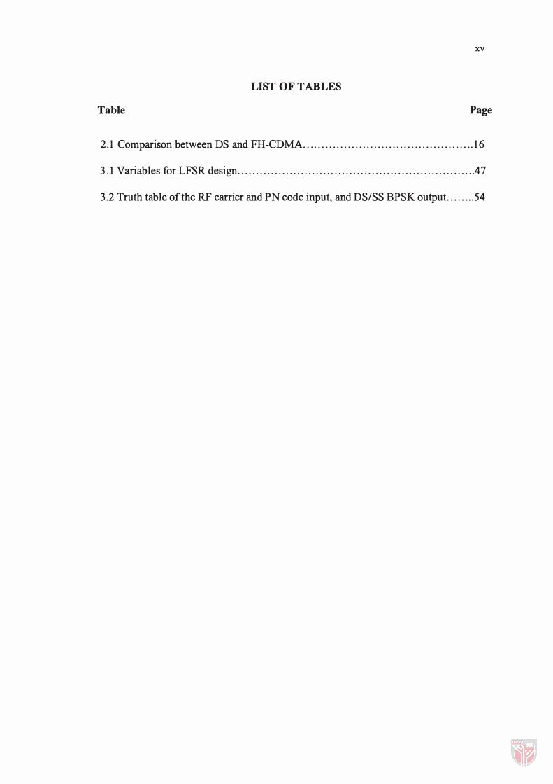
2. 1 Comparison between DS and FH-CDMA . . . . . . . . . . . . . . . . . . . . . . . . . . . . . . . . . . . . . . . . . . . . . . 1 6
3 . 1 Variables for LFSR design . . . . . . . . . . . . . . . . . . . . . . . . . . . . . . . . . . . . . . . . . . . . . . . . . . . . . . . . . . . . . . . .47
3 .2 Truth table of the RF carrier and PN code input, and DS/SS BPSK output. . . . . . . . 54
XVI
LIST OF FIGURES
Figure Page
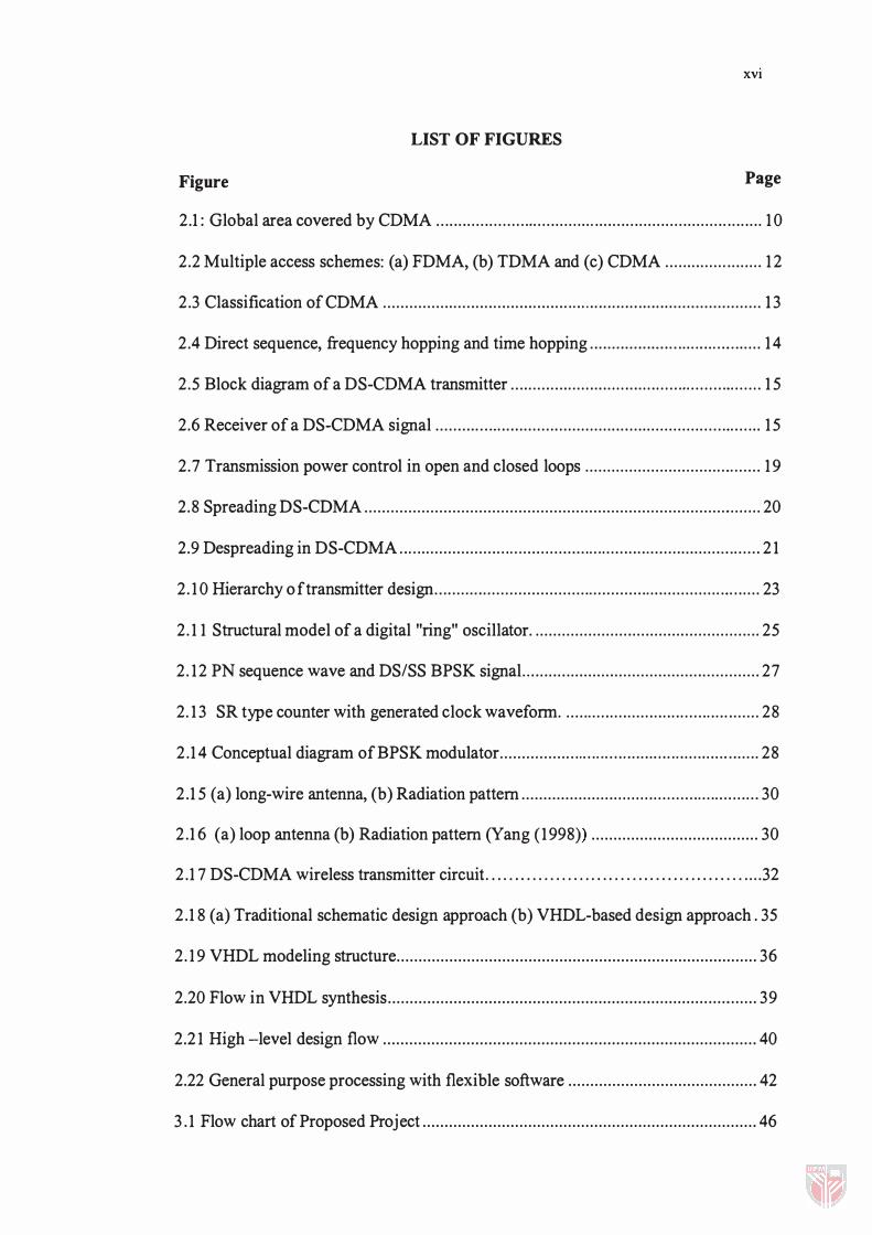
2.1: Global area covered by CDMA ................................... . ...................................... 10
2.2 Multiple access schemes: (a) FDMA, (b) TDMA and (c) CDMA ...................... 12
2.3 Classification of CDMA .............................................. ........................................ 13
2.4 Direct sequence, frequency hopping and time hopping ........................ ........ ....... 14
2.5 Block diagram of a DS-CDMA transmitter ......................................................... 15
2.6 Receiver of a DS-CDMA signal .......................................................................... 15
2.7 Transmission power control in open and closed loops ................................ ........ 19
2.8 Spreading DS-CDMA .......................................................................................... 20
2.9 Despreading in DS-CDMA ........................... ................................................ ....... 21
2.1 0 Hierarchy of transmitter design .......................................................................... 23
2.1 1 Structural model of a digital "ring" oscillator . ................................................... 25
2.12 PN sequence wave and DS/SS BPSK signaL .................................................... 27
2.13 SR type counter with generated clock waveform . ............................................ 28
2.14 Conceptual diagram of BPSK modulator ........................................................... 28
2.15 (a) long-wire antenna, (b) Radiation pattern ...................................................... 30
2.16 (a) loop antenna (b) Radiation pattern (Yang (1998» ...................................... 30
2.17 DS-CDMA wireless transmitter circuit . . . . ... . . . . . . . . . . . .. .. . . . . .. . .. . . .. .. . . . . . . . .... 32
2.18 (a) Traditional schematic design approach (b) VHDL-based design approach . 35
2.19 VHDL modeling structure .................................................................................. 36
2.20 Flow in VHDL synthesis .................................................................................... 39
2.21 High -level design flow ..................................................................................... 40
2.22 General purpose processing with flexible software ........................................... 42
3.1 Flow chart of Proposed Project ............................................................................ 46
xvii
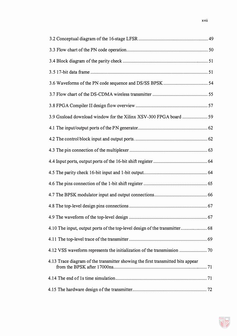
3 .2 Conceptual diagram ofthe 1 6-stage LFSR . . . . . . . . . . . . . . . . . . . . . . . . . . . . . . . . . . . . . . . . . . . . . . . . . . . . . . . . . . 49
3.3 Flow chart of the PN code operation . . . . . . . . . . . . . . . . . . . . . . . . . . . . . . . . . . . . . . . . . . . . . . . . . . . . . . . . . . . . . . . . . . . . 50
3 .4 Block diagram ofthe parity check . . . . . . . . . . . . . . . . . . . . . . . . . . . . . . . . . . . . . . . . . . . . . . . . . . . . . . . . . . . . . ... . . . . . . . 5 1
3 . 5 1 7-bit data frame .................................................................................................. 5 1
3 .6 Waveforms ofthe PN code sequence and DS/SS BPSK . . . . . . . . . . . . . . . . . . . . . . . . . . . . . . . .. . . . . 54
3.7 Flow chart of the DS-CDMA wireless transmitter . . . . . . . . . . . . . . . . . . . . . . . . . . . . . . . . . . . . . . . . . . . . . . 55
3 .8 FPGA Compiler II design flow overview . . . . . . . . . . . . . . . . . . . . . . . . . . . . . . . . . . . . . . . . . . . . . . . . . . . . . . . . . . . . 57
3 .9 Gxsload download window for the Xilinx XSV-300 FPGA board . . . . . . . . . . . . . . . . . . . . . 59
4.1 The input/output ports of the PN generator . . . . . . . . . . . . . . . . . . . . . . . . . . . . . . . . . . . . . . . . . . . . . . . . . . . . . . . . . . 62
4.2 The control block input and output ports . . . . . . . . . . . . . . . . . . . . . . . . . . . . . . . . . . . . . . . . . . . . . . . . . . . . . . . . . . . . . 62
4.3 The pin connection of the multiplexer . . . . . . . . . . . . . . . . . . . . . . . . . . . . . . . . . . . . . . . . . . . . . . . . . . . . . . . . . . . . . . . . . 63
4.4 Input ports, output ports of the 16-bit shift register . . . . . . . . . . . . . . . . . . . . . . . . . . . . . . . . . . . . . . . . . . . . . 64
4.5 The parity check 1 6-bit input and I -bit output. . . . . . . . . . . . . . . . . . . . . . . . . . . . . . . . . . . . . . . . . . . . . . . . . . . . . 64
4.6 The pins connection ofthe I -bit shift register . . . . . . . . . . . . . . . . . . . . . . . . . . . . . . . . . . . . . . . . . . . . . . . . . . . . . 65
4.7 The BPSK modulator input and output connections . . . . . . . . . . . . . . . . . . . . . . . . . . . . . . . . . . . . . . . . . . . . 66
4.8 The top-level design pins connections . . . . . . . . . . . . . . . . . . . . . . . . . . . . . . . . . . . . . . . . . . . . . . . . . . . . . . . . . . . . . . . . . 67
4.9 The waveform of the top-level design . . . . . . . . . . . . . . . . . . . . . . . . . . . . . . . . . . . . . . . . . . . . . . . . . . . . . . . . . . . . . . . . . 67
4.10 The input, output ports of the top-level design of the transmitter. .... .... . ... . . .. . . .. . 68
4.1 1 The top-level trace of the transmitter . . . . . . . . . . . . . . . . . . . . . . . . . . . . . . . . . . . . . . . . . . . . . . . . . . . . . . . . . . . . . . . . . 69
4. 12 VSS waveform represents the initialization ofthe transmission . . . . . . . . . . . . . . . . . . . . . . . 70
4. 1 3 Trace diagram of the transmitter showing the first transmitted bits appear from the BPSK after 1 7000ns . . . . . . . . . . . . . . . . . . . . . . . . . . . . . . . . . . . . . . . . . . . . . . . . . . . . . . . . . . . . . . . . . . . . . . . . . . . . . . 7 1
4. 1 4 The end of I s time simulation . . . . . . . . . . . . . . . . . . . . . . . . . . . . . . . . . . . . . . . . . . . . . . . . . . . . . . . . . . . . . . . . . . . . . . . . . . . . 7 1
4. 1 5 The hardware design of the transmitter. . . . . . . . . . . . . . . . . . . . . . . . . . . . . . . . . . . . . . . . . . . . . . . . . . . . . . . . . . . . . . 72

AMPS
CDMA
DS
FH
FHMA
FHSS
FSK
JTIDS
LAN
LPI
NMT
PN
RF
SNR
SS
SSMA
TACS
TxPC
UPM
LIST OF ABBREVIATIONS
Advanced Mobile Phone Service
Code Division Multiple Access
Direct Sequence
Frequency Hopping
Frequency Hopping Multiple Access
Frequency Hopping Spread Spectrum
Frequency Shift Keying
Join Tactical Information Distribution System
Local Area Network
Low Probability of Intercept
Nordic Mobile Telephone
Pseudo-Noise
Radio Frequency
Signal to Noise Ratio
Spread Spectrum
Spread Spectrum Multiple Access
Total Access Communications System
Transmit Power Control
Universiti Putra Malaysia
XVlll

CHAPTER 1
INTRODUCTION
1.1 Background of the Study
Code Division Multiple Access (CDMA) is a radically new concept in wireless
communications. It has taken cellular radio systems by storm with its potential to
dramatically increase both the system capacity and service quality. CDMA is a
spread spectrum technology in that it spreads the information from a narrowband
signal over a much broader bandwidth.
One of the most important concepts to cellular telephony is multiple access which
allows several users to be supported simultaneously. In other words, several users
share a pool of channels with any user able to use any channel and no channel
assigned to any user. A channel is therefore merely a part of the radio resource,
temporarily allocated for a call. Multiple access is therefore just how a radio
spectrum is divided into channels and how the channels are allocated to the several
users of the system.
2
CDMA architecture is based on the spread-spectrum technique (Tabbane, 2000),
initially developed by the military because of its usefulness in tactical environments.
It is used, for instance, in GPS as part of the tactical information distribution system
(JTIDS). The core principle of spread spectrum is to use noise-like carrier waves in,
as the name implies, a bandwidth much wider than that required for simple point-to
point communication at the same data rate. Militarily there were two advantages - it
is impossible to jam by the enemy (anti-jam, or AJ) and masks the fact that
communication is taking place. Thus, in military parlance, it was called low
probability intercept (LPn. Although first used in the early days of World War II, it
was only in 1978 that spread-spectrum techniques were proposed for high capacity
cellular mobile communications systems.
There are two main techniques involved - Frequency Hopping (FH) and Direct
Sequence (DS). DS is also called Code Division Multiple Access (CDMA). In both
techniques, synchronization of the transmitter and receiver is required. Both use a
pseudo-random carrier, but the carrier is created in different ways.
Rahman (2000) recorded that the Direct Sequence Spread Spectrum (DS-SS) uses a
code sequence with a bit rate higher than the digital data bit rate to be transmitted.
The carrier signal is modulated by the code sequence resulting in a wideband signal
from the transmitter. The process is reversed at the receiver to regenerate the data
transmitted.
In CDMA, each station is allocated a random sequence or code. This sequence is
unique to the station and must be orthogonal or quasi-orthogonal (i.e. decorrelated)
3
with all the other sequences. In FH-COMA, the code is used to generate a unique
hopping sequence. In OS-COMA, the code is used to make a quasi-random (i.e.
similar to noise) high rate transmitted signal combined with the information spread
the spectrum.
A transmitter is linked to the receiver by radio waves to the allocated base station, or
cable line (wired) to a computer allowing the computer to transmit/receive data from
a similarly equipped remote control.
1.2 Problem Statement
There are many types of electronic circuits used for transmission with different
options for OS-COMA. The use of some circuitry was dictated by the availability of
a particular IC, or because a portion of a quad gate was yet unused. Some circuits
using passive components also need high power to drive the circuit. The addition to
the high power needed the passive circuits is altered to decrease the circuit operations
of transmission, when the transmitter operates with long time duration. These effects
appear as thermal heat that increases the passive components values and decrease the
efficiency of transmission. However, the circuit used is easy to implement and
simplify.
For these reasons, OS-COMA wireless transmitter using FPGA is regarded as a
promising technique for future COMA networks. The transmitter is mainly used
digital components such as flip-flops, gates, etc., which leads the transmission in
higher performance.
4
1.3 Significance of the Study
Wireless communications with mobile and cellular radio technology is experiencing
its fastest growth ever, particularly in the past 1 0 years. It has already progressed
from the first generation ( IG) to second generation (2G) which uses Frequency
Division MUltiple Access (FDMA) and Time Division Multiple Access (TDMA). In
the new millennium the world is about to receive the third generation, which is
predicated on higher data rate and better spectrum efficiency to enable wireless data
communication in full multimedia.
In 3G, the information transferred is not limited to having voices, images and digital
data separately. Users will have full coverage and mobility for 144 kbps (preferably
348 kbps) and eventually up to 2 Mbps limit. With this wideband, users are able to
access the information in full multimedia form, wirelessly and with better quality.
1.4 Objectives of the Thesis
The objectives of this study were to:
1 . Study the spread-spectrum DS-CDMA concept, especially the PN coding
system.
2. Study BPSK modulation in the DS-CDMA system.
3 . Implement PN coding and BPSK modulation in the DS-CDMA transmitter
circuit using digital transmission.
4. Design, simulate and synthesize the PN coding, BPSK modulation, Oscillator
and Parity Check, using the VHDL source code.
5. Create the top-level design file for the DS-CDMA wireless transmitter using
the VHDL source code for PN coding, BPSK modulation, Oscillator and
Parity Check, using the FPGA compiler II.
6. Download the design into a Xilinx FPGA board.
1.5 Constraints of the Project
This thesis describes the DS-CDMA wireless transmitter design using FPGA. The
DS-CDMA wireless transmitter is expected to transmit at data rates up to 2 Mbps
with error detection and 40 MHz carrier frequency. The Synopsys package was used
as the simulation and synthesis tool (FPGA compiler II and VHDL). The Synopsys
package allows easy reconfiguration of the transmitter. The design steps using this
software depend mainly on the design components and the system configuration. The
applicability of certain frequencies depends on the system application and design
scenario. For this transmitter, the frequency carrier depends on the hardware (FPGA
board) and the system components of the transmitter circuit. The FPGA board has a
maximum frequency of 100 MHz. Some frequency dividers had to be used as shown
in Appendix 22 to slow the frequency down to below this speed. For this project, a
clock of 2 MHz was used. For the simplified design, a 40 MHz speed was used with
two frequency dividers, multiplying the clock speed by 2 and 1 0 times.
The function of any communication system is to carry information - as voice, video
or digital signals. To carry the information, a band is required. To send more
information, a broader band or more time is required with a trade-off between the
two. Other factors are also involved - the power pushing the signal through and the
6
clutter (noise) in the band. Shannon's law of channel capacity relates the maximum
rate of data transfer as follows:
. . (signa/power J Capaczty = bandwzdth * /og2 1 + --=�.---=---nozsepower
with capacity in bits per second, bandwidth in hertz and signal and noise powers in
the same physical units, such as watts. From the equation, the relationship between
capacity and bandwidth is linear. Doubling the bandwidth therefore doubles the
capacity. In contrast, the effects of signal power and noise power are logarithmic and
therefore less dramatic. A large increase in power will result in a less than
proportionate increase in the capacity (Schweber, 1991).
The XSV board has a variety of interfaces for communicating with the outside world:
parallel and serial ports, Xchecker cable, a USB port, PS/2 mouse and keyboard port
and 1 0/100 Ethernet PHY layer interface. There are also two independent expansion
ports, each with 38 general-purpose 110 pins connected directly to the Virtex FPGA.
The board can be configured through the parallel port, serial port, Xchecker cable or
from a bit stream stored in the 16 M bit Flash RAM. The Flash RAM can also store
data for use by the FPGA after the configuration is complete. The complete features
of the XSV FPGA board were discussed in Appendix 23.
To extend the project to the analog portion of the transmitter, a special version of
VHDL called VHDL-AMS can be used for analog-mixed signal and might be able to
be used for analog system design. However, VHDL-AMS capability has to be
investigated first as a feasibility study.