universiti tun hussein onn malaysia status...
TRANSCRIPT
UNIVERSITI TUN HUSSEIN ONN MALAYSIA
STATUS CONFIRMATION FOR MASTER’S THESIS
IMPROVEMENT ON SPOC+ TEST PROGRAM WITH AMBIENT TEST REMOVAL
ACADEMIC SESSION : 2015/2016
I, HANA NABILA BINTI MOHD EFFENDI agree to allow this Master’s Project Report to be kept at the Library under the following terms:
1. This Master’s Project Report is the property of the Universiti Tun Hussein Onn Malaysia. 2. The library has the right to make copies for educational purposes only. 3. The library is allowed to make copies of this report for educational exchange between higher
educational institutions. 4. ** Please Mark (√)
CONFIDENTIAL (Contains information of high security or of great
importance to Malaysia as STIPULATED under the OFFICIAL SECRET ACT 1972)
RESTRICTED (Contains restricted information as determined by the
organization/ institution where research was conducted) FREE ACCESS
Approved by,
__________________________________ __________________________________
(WRITER’S SIGNATURE) (SUPERVISOR’S SIGNATURE)
Permanent Address: Supervisor’s Name NO 18, JALAN KELISA 2, DR. NAN BIN MAD SAHAR TAMAN SUNGAI ABONG INDAH, 84000 MUAR, JOHOR DARUL TAKZIM. DATE: 17TH JANUARY 2016 DATE: 17TH JANUARY 2016
NOTE: ** If this Master Project Report is classified as CONFIDENTIAL or RESTRICTED,
please attach the letter from the relevant authority/organization stating reasons and duration for such classifications.
√
i
IMPROVEMENT ON SPOC+ TEST PROGRAM WITH AMBIENT TEST
REMOVAL
HANA NABILA BINTI MOHD EFFENDI
A project report submitted in partial
fulfillment of the requirement for the
Master of Electrical Engineering
Faculty of Electrical and Electronic Engineering
Universiti Tun Hussein Onn Malaysia
Jan 2016

ii
I hereby declare that the work in this project is my own except for quotations and
summaries which have been duly acknowledge
Student :……………………………………………………
HANA NABILA BINTI MOHD EFFENDI
Date :……………………………………………………
Supervisor :…………………………………………………….
DR NAN BIN MD SAHAR

iii
DEDICATION
This thesis is dedicated to
Father: Hj Mohd Effendi bin Ahmad
Mother: Hjh Rela binti Abdul Rahman
Husband: Mohd Azrin Abd Rahman
Sister: Siti Nadia binti Mohd Effendi
Brother: Nur Fikri bin Mohd Effendi

iv
ACKNOWLEDGEMENTS
It is a genuine pleasure to express my deep sense of thanks and gratitude to Allah
S.W.T for giving me a chance to breathe to continue my study in Master of Electrical
Engineering. Besides that, thanks to my supervisor and guider, Dr. Nan bin Md.
Sahar. His dedication and keen interest in his entire overwhelming attitude to help
his students had been solely and mainly responsible for completing my work. His
timely advice and scientific approach have helped me to a very great extent to
accomplish this task.
It is my privilege to thank my parents, my husband and my siblings, for their
constant encouragement throughout my study period. Their prayer and support are
always with me and this is the one that give me courage to continue this study.
I would like to thank UTHM for giving me opportunity to continue my study
in this university, Not to forget, my company Infineon Technologies Sdn Bhd for
giving me a chance to complete this project.
Besides that, not to forget my friends and colleagues for providing me
necessary technical suggestions during my project pursuit. Appreciation also goes to
everyone involved direct or indirectly towards the compilation of this thesis.

v
ABSTRACT
Semiconductor is one of the elements that can conduct electricity with
certain conditions by making it a good medium to control the electric current.
Automotive applications are one of the higher demands in semiconductor
industries because in automotive technologies, revolutions have been driven
into two motivations which are maximizing comfort and applying zero
defects method. The market demands of automotive chips are increasing with
the higher demand of new vehicle. As semiconductor industries, the
improvement in accomplish the customer request is our main vision with zero
defects and low cost. These project objectives are to improve test yield, to
implement ambient test removal, to save cost in production line and to reduce
the test time. During the studies, all the root cause of high failure reject is
analyse by finding the root cause. The analysis of the root cause is finding by
using Root Cause Analysis and performs distribution from data extraction
using CEDA analysis software. The comparison yield from each temperature
had been made. The analysis finding that the low yield is because of the test
program is not optimized in Revision 2.04. The test program revision 2.05
had been updated with the new limit by using six sigma calculations. From
the test program update, the monitoring is continued to check the stability of
the test program to continue with the ambient test removal. Ambient test
removal analysis had been performed with 3x77pcs data collection to
calculate the new limit parameter at cold and warm. With the new limit
setting, 10k data verification is continue to check whether cold and warm test
can segregate all the rejects. In this case, the test results at ambient test must
be 100% pass. This entire works gives a result where test yield improve from
97% to 99%, remove ambient test, save cost from buying extra handler which
cost € 954,723 and test time reduction from 11 days to 7days.

vi
ABSTRAK
Semikonduktor adalah elemen yang menguruskan aliran elektrik dalam
sesuatu keadaan untuk menjadikan ianya satu medium terbaik untuk mengawal arus
elektrik. Automotif adalah antara permintaan tertinggi di dalam semikonduktor
industrI kerana di dalam teknologi automotif, revolusi telah didorong kepada dua
motivasi iaitu memaksimakan keselesaan dan mengaplikasi sifar kerosakan.
Permintaan pemasaran untuk cip automotif semakin meningkat dengan peningkatan
kenderaan baharu. Sebagai semikonduktor industri, penambahbaikkan untuk
menunaikan permintaan pelanggan adalah visi utama dengan sifar kerosakan dan kos
yang rendah. Oleh itu, kajian ini akan mempersembahkan bagaimana untuk
mencapai permintaan pelanggan dengan melakukan pengurangan kos di
semikonduktor industri. Objektif projek ini adalah peningkatan hasil, perlaksanaan
pembuangan suhu bilik, penjimatan kos di ruang produksi dan pengurangan ujian
masa. Semasa kajian, punca kerosakan akan dianalisa dengan melakukan “Root
Cause Analysis (RCA)“ dan pengekstrakan data. Selain daripada itu, permbandingan
kadar hasil untuk setiap suhu dilakukan. Kajian mendapati kadar hasil rendah adalah
disebabkan program ujian tidak optimum dalam revisi 2.04. Program ujian revisi
2.05 telah dikemaskini dengan had terbaru menggunakan kiraan “six sigma”.
Daripada kemaskini terbaru untuk program ujian, pemantauan diteruskan untuk
memastikan kestabilan ujian program. “Ambient test removal“ analisa menggunakan
3x77 koleksi data untuk mengira had terbaru pada suhu sejuk dan panas. Dengan
menggunakan had terbaru, 10k verifikasi data diteruskan untuk memastikan ujian di
suhu sejuk dan panas mampu mengasingkan unit yang rosak. Dalam kes ini,
keputusan ujian mestilah 100% lulus. Keseluruhan kerja ini memberi keputusan di
mana kadar hasi meningkat dari 97% ke 99%, pembuangan suhu bilik, penjimatan
kos dari membeli mesin tambahan bernilai € 954,723 dan pengurangan kadar masa
dari 11 hari ke 7 hari.

vii
CONTENTS
TITLE i
DECLARATION ii
DEDICATION iii
ACKNOWLEDGEMENT iv
ABSTRACT v
ABSTRAK vi
CONTENTS vii
LIST OF TABLES x
LIST OF FIGURES xii
LIST OF SYMBOLS AND ABBREVIATIONS xiv
CHAPTER 1 INTRODUCTION 1
1.1 Background of Study 1
1.2 Problem Statement 3
1.3 Objectives 5
1.4 Scope of the Projects 5
1.5 Thesis Organization 6
1.5.1 Chapter One: Introduction 6
1.5.2 Chapter Two: Literature Review 6
1.5.3 Chapter Three: Methodology 6
1.5.4 Chapter Four: Data Analysis and Results 7
1.5.5 Chapter 5: Conclusions and 7
Recommendation
1.6 Conclusions 7

viii
CHAPTER 2 LITERATURE REVIEW 8
2.1 Introduction 8
2.2 Growth of Automotive Devices 8
2.3 Test Yield 11
2.4 Techniques Comparison for Cost Reduction in 12
Semiconductor Industries
2.5 Automotive product – SPOC+ 15
2.5.1 Types of SPOC+ product 16
2.5.2 Function of SPOC+ 19
2.6 Final Test Concept 20
2.6.1 Testing Flow 20
2.6.2 Micro Flex Tester 22
2.7 Conclusion 23
CHAPTER 3 METHODOLOGY 25
3.1 Introduction 25
3.2 Framework of Research 28
3.3 Phase 1: Analyse Data 28
3.3.1 Root Cause of Yield Losses 29
3.3.2 Test Program Improvement and Test 34
Program Stability
3.4 Phase 2: ANALYSIS FOR AMBIENT TEST 38
REMOVAL
3.5 Conclusions 41
CHAPTER 4 RESULTS AND DATA ANALYSIS 42
4.1 Introduction 42
4.2 Results for First Objectives 42
4.2.1 Root Cause Analysis 48
4.2.1.1 Leakage Failure at Hot Test 50
4.2.1.2 ESD Failure at Ambient Test 60
4.3 Results for the Second, Third and Fourth Objectives 66
4.4 Conclusions 82
CHAPTER 5 CONCLUSIONS AND RECOMMENDATION 83
5.1 Introduction 83

ix
5.2 Project Achievement 83
5.2.1 Improvement on Testing Yield for SPOC+ 84
5.2.2 Implementation of Ambient Test Removal, 84
Cost Savings and Test Time Reduction
5.3 Conclusion 85
5.4 Recommendations for Further Studies 86
REFERENCES 87
BIBLIOGRAPHY 88

x
LIST OF TABLES
2.1 Temperature Specifications for Standard and High 17
Temperature Applications
2.2 Current Method of Cost Reduction in Semiconductor Industries 13
2.3 Comparison between Method 1, 2, 3 and Ambient Test Removal 15
3.1 Losses category 31
3.2 Is/Is Not analysis example 32
3.3 Electrical characteristic for current through Vdd pin 37
4.1 Limit changes in SPOC+ test program 43
4.2 10 lots monitoring results for Ambient Test 44
4.3 10 lots monitoring results for Cold Test 45
4.4 10 lots monitoring results for Hot Test 46
4.5 Is/Is Not cause analysis table 49
4.6 Calculation USL and LSL by using excel software 63
4.7 3x77pcs data collection results 67
4.8 Excel calculation upper side limit and lower side limit for 68
Cold Test Device BTS56033-LBx
4.9 Excel calculation upper side limit and lower side limit for 69
Hot Test Device BTS56033-LBx
4.10 Excel calculation upper side limit and lower side limit for 70
Cold Test Device BTS54220-LBx
4.11 Excel calculation upper side limit and lower side limit for 71
Hot Test Device BTS54220-LBx
4.12 Excel calculation upper side limit and lower side limit for 72
Cold Test Device BTS54040-LBx
4.13 Excel calculation upper side limit and lower side limit for 72
Hot Test Device BTS54040-LBx
4.14 10k verification results for BTS56033-LBA, 73

xi
BTS54040-LBA and BTS54220-LBE
4.15 New flow after ambient test removal 74
4.16 Comparison results of savings and reduction in production 75
4.17 Tester cost including accessories 80
4.18 Tester cost including accessories 81

xii
LIST OF FIGURES
1.1 Global semiconductor billings – forecast by application 2
(source from PwC analysis, 2014)
1.2 Total demand SPOC+ (kpcs/week) 3
1.3 Failure percentage 2014/2015 for SPOC+ product 4
2.1 Key drivers for future automotive growth 9
(source from PWC analysis, 2013)
2.2 Comparison yield between three temperatures in SPOC+ 14
2.3 Block diagram of BTS54220-LBx 17
2.4 Block diagram of BTS55032-LBx 18
2.5 Block diagram of BTS56033-LBx 18
2.6 Block diagram of BTS54040-LBx 19
2.7 Process flow of fabricating and testing SPOC+ device 21
2.8 Micro FLEX system block diagram 23
3.1 Flow of methodology phase 1 - Analysing data 26
3.2 Flow of methodology phase 2 – Analysis for ambient test removal 27
3.3 Flow of final test 29
3.4 Overall test yield for SPOC+ 30
3.5 Losses SPOC+ from Jan’15 to March’15 33
3.6 SPOC+ test program division 34
3.7 Corner-stone version 5.3 (CEDA) 34
3.8 Step 1 to perform correlation plot/ cumulative frequency. 35
3.9 Step 2 to perform correlation plot/ cumulative frequency. 36
3.10 Correlation plot Ivsstb_mx_18r vs Temp_checki 37
3.11 Comparison yield between three temperatures 38
(ambient, cold and warm test)
4.1 Yield for Ambient Test 44
4.2 Yield at Cold Test 45

xiii
4.3 Yield at Hot Test 46
4.4 Comparison yield test program revision 2.04 versus test 47
Program revision 2.05
4.5 Reject pareto at Hot Test (revision 2.04) 50
4.6 Correlation plot Ivsstb_mx_18r vs Temp_checki 51
4.7 Correlation plot Ivsstb_35r vs Temp_checki 52
4.8 Correlation plot Ivsstb_35i vs Temp_checki 53
4.9 Correlation plot Ivsstb_mx_18i vs Temp_checki 53
4.10 Recovery percentage 54
4.11 Correlation plot Ivsstb_35r 55
4.12 Correlation plot Ivsstb_mx_18i 55
4.13 Correlation plot Ivsstb_35i 56
4.14 Correlation plot Ivsstb_mx_18r 57
4.15 Reject pareto at Hot Test 58
4.16 Correlation plot for Ivsstb_35r for Hot Test 58
4.17 Correlation plot for Ivsstb_35i for Hot Test 59
4.18 Correlation plot for Ivsstb_mx_18r for Hot Test 59
4.19 Correlation plot for Ivsstb_mx_18i for Hot Test 59
4.20 ESD measurement diagram 61
4.21 ESD_EDOIN3R percentage ratio 61
4.22 Cumulative plot of ESD_EDOIN3R for BE sample run. 62
4.23 Cumulative plot of ESD_EDOIN3R for FE sample run. 62
4.24 Cumulative trend plot with the new limit. 64
4.25 ESD_EDOINxx – BE Cold Test 1 Year Trend Plot 65
4.26 ESD_EDOINxx – BE Hot Test 1 Year Trend Plot 65
4.27 Critical parameter with low cpk value 76
4.28 Yield first test versus verification yield at Ambient Test 77
4.29 Comparison machine required before ATR and after ATR 78
4.30 Total day to complete testing before ATR versus after ATR 78

xiv
LIST OF SYMBOLS AND ABBREVIATIONS
CAAGR - Compounded Average Annual Growth Rate
PCA - Principal Component Analysis
RSM - Response Surface Modelling
OEE - Overall Efficiency Equipment
SPI - Serial Peripheral Interface
CMOS - Complementary metal–oxide–semiconductor
PWM - Pulse Width Modulation
RoHS - Restriction of Hazardous Substances
AEC - Automotive Electronics Council
LED - Light Emitting Diode
DMOS - Diffusion Metal Oxide Semiconductor
ILLIM - Internal Leakage Limit
Pb-free - Lead-free
EMO - Emergency Machine Off
GPIO - General Purpose Input Output
SBA - Semiconductor Business Association
EDD - Electrostatic Detection Devices
EDO - Electrostatic Detection output
USL - Upper Side Limit
LSL - Lower Side Limit
Rev - Revision
ESD - Electrostatic Discharge

xv
BE - Back End
FE - Front End
± - Plus/ Minuse (Range)
uA - micro Ampere
GND - ground
IN - Input
$ - Dollar Sign
ms - milli second
V - voltage
RM - Ringgit Malaysia
USD - US Dolar
SGD - Singapore Dolar
€ - Euro

1
CHAPTER 1
INTRODUCTION
1.1 Background of Study
Semiconductor is element that can conduct electricity with certain conditions by
making it a good medium to control the electric current. Conductivity for
semiconductor device is depending on the current and voltage applied to control
electrode. For basic knowledge about semiconductor, properties of semiconductor
are depending on the impurities in the component itself. Like N-type and P-type
semiconductor, they carry current mainly in the form of negatively-charges electron
and positively-charges holes respectively.
In automotive technologies, revolutions have been driven in two motivations
which are to maximize comfort and apply zero defects methods (no accidents and
eco-hazards). Semiconductor devices, microelectromechanical systems (MEMS) and
electric motors have been replaced many mechanical parts to make vehicles safer,
more comfortable and eco-friendly.
Market demand of new vehicle in short term is uncertainties and continuous
weak. Automotive industry of environment safety, information and affordable cars
will continue drive growth opportunities in automotive semiconductor industry
market. Webber (2013) report that automotive semiconductor market worth almost $
26 billion in 2012, these industry imperatives are expected to drive market revenue at

2
a Compounded Average Annual Growth Rate (CAAGR) of 7.4% over the five year
period 2012 to 2017.
All applications in semiconductor industries require high power management
with achievement of analogue integrated circuits (ICs) and discrete components.
Segment grew 24 percent in 2014 and target to increase another 22 percent in 2015,
making it the fastest growing sector in automotive market. Figure 1.1 shows the
global semiconductor billings according to applications.
Figure 1.1: Global semiconductor billings – forecast by application (source from
PwC analysis, 2014)
Since automotive application demand is become high, it is very important for
semiconductor industry to do improvement in order to meet customer delivery.
Improvement in semiconductor industries can involve in many areas which is
improvement on wafer at Front End, equipment, and test program improvement to
avoid high losses in the product yield.
Improvement must be done on the failing Integrated Circuit (IC). This thesis
report will discussed on test program improvement, Test program improvement is the
process of collecting and analysing data to determine the root cause of a high over
3
rejection to improve the product yield. It is an important discipline in many branches
of manufacturing industry where it is a tool used in the development of the new
products or improvement of existing products. The reason of the stability test
program is to give evidence on how the quality of the IC with moment under the
influence of a multiplicity of ecological factors such as humidity, temperature,
storage conditions and IC life failure. Effective root cause analysis of part failures is
required to assure corrective action can be implemented to stable the test program.
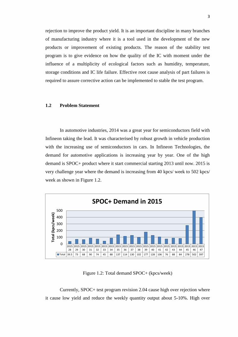
1.2 Problem Statement
In automotive industries, 2014 was a great year for semiconductors field with
Infineon taking the lead. It was characterised by robust growth in vehicle production
with the increasing use of semiconductors in cars. In Infineon Technologies, the
demand for automotive applications is increasing year by year. One of the high
demand is SPOC+ product where it start commercial starting 2013 until now. 2015 is
very challenge year where the demand is increasing from 40 kpcs/ week to 502 kpcs/
week as shown in Figure 1.2.
Figure 1.2: Total demand SPOC+ (kpcs/week)
Currently, SPOC+ test program revision 2.04 cause high over rejection where
it cause low yield and reduce the weekly quantity output about 5-10%. High over
201528
201529
201530
201531
201532
201533
201534
201535
201536
201537
201538
201539
201540
201541
201542
201543
201544
201545
201546
201547
Total 39.5 73 68 90 74 45 88 137 114 130 102 177 128 106 76 88 84 278 502 397
0
100
200
300
400
500
Tota
l (kp
cs/w
ee
k)
SPOC+ Demand in 2015

4
rejection can be attributed to Electrostatic Discharge (ESD), leakage, temperature
setup and handling issue. Figure 1.3 shows the details of high over rejection (65%
failure rate) for SPOC+ product in production line.
Figure 1.3: Failure percentage 2014/2015 for SPOC+ product
This study begins to address issues of high over rejections by analyse the root
cause to ensure the test program stability. Besides that, this project will discuss the
new technique of improvement to support customer demand by reduce the test
insertion.
65% 11%
10%
8% 5% 1%
Failure Percentage 2014/2015
Over Rejection
Product Issue (Known)
No Die/No Wire
Others (Major)
Abnormal Stoppages (Mech)
Missing/Incomplete TestSummary

5
1.3 Objectives
The objectives of the project are:
i) To investigate the problem of high yield losses for SPOC+ testing due to
test program not optimize in order to improve testing yield for SPOC+.
ii) To do implementations ambient test removal for SPOC+ with the new
limit changes in Cold test and Hot Test in order to support ramp up.
iii) To save cost for SPOC+ production line from buying extra machine
during production ramp up.
iv) To do test time reduction in order to meet weekly customer demand
especially when device ramp up.
1.4 Scope of the Project
The scope of this project consist several parts which are root cause analysis that will
be performed by using Is/Is Not Cause table analysis and cumulative frequency data
by using CEDA, 10lots monitoring, ambient test removal assessment. Besides that,
after ambient test removal implementation, the cost savings and test time reduction
will calculate in order to make sure objective is achieved. In ambient test removal
assessment, the new limit will be calculate based on 3x77pcs data collection and
continue with 10k verification data to identify either cold and warm test able to
segregate the rejects or not.

6
1.5 Thesis Organisation
The aim of this project is addressed in five chapters. Every chapter is arranged to
definite the objective so that it can be achieved using the systematic structure.
1.5.1 Chapter One: Introduction
This chapter begins with the introduction about the project. It is more to explore
about the current issued happen in testing production for SPOC+. Other than that, the
problem statement, objectives of the study, methodology, and structure of the
research are explained through this chapter.
1.5.2 Chapter Two: Literature Review
Literature reviews are related under this chapter. The matter discussed is the
introduction in this chapter, definition of automotive, marketing in automotive
device, SPOC+ functions and type of SPOC+. In addition, the DELTA MATRIX
machine, yield and micro Flex tester are also explained in this chapter.
1.5.3 Chapter Three: Methodology
This chapter presents execution of data collecting and description of the yield test.
This chapter discussed more on yield losses and parameter failure by data collection
for three months. Data collection had been divided under two groups which are test
program improvement and ambient test removal. After the collection of the data, new
test program will be identified by performing remote debug and change the limit.
The methods of analysis are using e-Square and CEDA.

7
1.5.4 Chapter Four: Data Analysis and Results
This chapter obviously presents the data obtained and analysis by using selected
tools.
1.5.5 Chapter Five: Conclusions and Recommendation
The last chapter is about the conclusion for the whole research by generalizing the
findings by good yield and losses yield plotting. Other than that, findings, conclusion
and recommendations are discussed in this chapter. The analysis and the results in
the end of the research will implement a new test flow and reduce cost in production
for SPOC+ especially during ramp up.
1.6 Conclusions
This chapter is discussed about the project background, problem statement,
objectives, scope and thesis organisations. The automotive applications demand is
increase over year by year. As manufacturing industries, improvement of the IC
product must be continuous in order to meet customer satisfaction.
One of the high demands in Infineon Technologies is SPOC+ product.
However, the SPOC+ test program cause high over rejection and root cause analysis
will be performed for improvement. With the stability of the test program, the new
technique to support customer demand is introduced with remove one test insertion.
Besides that, more analysis is needed in order to understand each issue happen in
production line to support this project data analysis.

8
CHAPTER 2
LITERATURE REVIEW
2.1 Introduction
This chapter is an attempt to reveal the introduction of the importance and function
of the automotive devices in semiconductor industries. In the last two decades,
electronics and semiconductor technology had given major impact on the
functionality of automotive devices system. Now, with the electronic technology, a
well-established and recognized ingredient of modern automotive technology is
applied to achieve the objectives to replace electromechanical devices with improved
and move reliable electronic counterparts. Besides that, the objectives are
implementation of complex automatic control functions to replace and functionally
improve manual controls. Future cars will act as intelligent transportation and
information systems with high demand for application specific circuits and optimized
processes.
2.2 Growth of Automotive Device
Automotive device is challenging device in semiconductor industries. One of the
challenges is the increment demand from customer and semiconductor industry has

9
responsibility in achieving objectives to meet customer request. 2012 was a difficult
year for the global semiconductor industry. Chitkara & Ballhaus (2013) examined
those annual semiconductor billings in 2012 lagged by US$ 8 billion or 2.7 % behind
the record sales of US$ 300 billion achieved in 2011 due to continue global
economic challenges. However, semiconductor is growing master in the next year by
marketing, component, region and application.
Global semiconductor market suggests that billing will increase by some US$
109 billion in between 2012 and 2017 (Chitkara et al., 2013). Hence, the growth in
the automotive sector is divided into two major trends that is the extent and pace of
change in the industry itself. Besides that, the significantly higher proportion of
electronics have increased standard in automotive.
Key markets for automotive manufacturers are more cars and light vehicles
are now produced in emerging market that developed global economies. Brazil,
Russia, India and China are country that remains the most important growth driver
for global automotive demand. Average annual growth rates are between 6.5 % for
Brazil and 9.4 % for China for the years 2012-2017 (Chitkara et al., 2013). Figure
2.1 shows the key drives for future automotive growth.
Figure 2.1: Key drivers for future automotive growth (source from PWC analysis,
2013)

10
Semiconductor content per car is grown from US$ 315 in 2012 to US$ 700
by 2017, and the overall cost of electronics in cars is expected to reach more than 30
% by 2017 (Chitkara et al., 2013).
All innovation that is taking place in automotive is electronic compared to
mechanical innovations. A very significant portion of the growth in the industry will
continue to come from the desire of car makers, Tier 1 suppliers and semiconductor
companies to create and capture more value by offering innovations that will
improve the overall driving experience Chitkara et al., 2013).
The electronic component of automotive is expanding driven by several
concurrent forces, energy efficiency, emission reduction, safety features, comfort and
being “fun” to drive. In semiconductor industries, automotive requires zero defects,
extended temperature range, and long life durability.
A study by Funaki, Balda and Junghans (2005) mentioned that IC were
packaged in high temperature packages to measure the dc characteristics of these
Silicon Carbide (SiC) devices at ambient temperatures ranging from 25 (room
temperature) up to 450 . The automotive device is designed and built in accordance
with the static characteristics of the IC devices measured under extremely high
temperature of 400 . The conduction loss of IC increases slightly with increasing
temperature as predicted from its characteristics but it switching characteristics
hardly changes. Automotive IC’s product must be able to function in all
environments starting from cold, ambient and hot temperature (Funaki et al., 2005).
Since, automotive environment is current trends in automotive industry, it
will contribute the temperature envelope for electronic components. In Infineon
technologies, SPOC+ is a component that applicable for temperature between -33
until 160 . Therefore, research had found that the used of spots on engine and in
the transmission, these large bodies do provide heat sinking to reduce temperature
rise due to power dissipation in control unit, and majority temperature for the
application will be at 150 or less by Johnson and Evans (2004). Table 2.1 shows
the temperature specifications for standard and high temperature applications.

11
Table 2.1: Temperature specifications for standard and high temperature applications
Application Temperature Range
Telecommunication −20 to 80
Automotive Under The Hood −40 to 125
Automotive On Engine −40 to 165
Well Logging −25 to 225
In motivation, automotive technology has to fulfil demands such as high
yield, high throughput, low cost, suitable for all temperature, fine pitch and
insensitivity to Printed Circuit Board (PCB) topography.
2.3 Test Yield
Yield is simply known as a ratio percentage of the “good” product over total product
in a production batch as stated in equation (2.1). The ideal goal of semiconductor
production manufacturing is to make each individual integrated circuit performs
according to product specification. Yield is categorized under several components
where each of the components required a distinct set of tools to understand and
improve. Three main components are:
i) Functional (defect driven)
ii) Parametric (performance driven)
iii) Production efficiency/ equipment utilization
𝑒 𝑒𝑑 𝑒 𝑑
x100% (2.1)
Al-Hashimi (2013) studied that SRAM cell based on electrical testing is
method to analyse defects which can help in improving yield of semiconductor
integrated circuits. Development of new technologies by continuous shrinkage of
critical dimensions cause a new challenge in design and manufacturing modern
12
integrated circuits as it become denser and smaller in size. This is one of the
challenges where the design rules cause highly vulnerable to physical defects.
Daasch and Shirley (2009) studied that the new frontier used is call statistic
test in order to do yield improvement. Statistical method is capable to reduce data for
decision making and optimization. The challenge has to find and understand
appropriately to continue growth the statistical test engineering.
Dupret (2014) presented a method to model a yield by using Principal
Component Analysis (PCA) and Response Surface Modelling (RSM). Both are well
known methods to model analogue circuit performance. Both methods demonstrated
to give a good results on yield modelling.
Even though the method to analyse the defects and yield is different, however
the collected data are similar. In order to analyse the failure, collected data such as
defects density measurements, electrical in line test measurements and final test data
are needed. Final test data is important and obtained from test pattern in order to
ensure assembled chips meets customer specifications.
2.4 Techniques Comparison for Cost Reduction in Semiconductor Industries
IC (Integrated circuit) is involved in continuous complexity process with the cheap
price. The IC’s complexity is increased by applying Moore’s Law. This complexity
increases and price decreases must parallel with quality of the products by applying
zero defects concept. Cost of production for each device is important for
manufacturers (semiconductor industries). This is strongly agreed with statement
from Deshayes (1998) where the cost aspect is particularly important for
microcontroller (MCU) manufacturers, since these devices are produced in volume,
and are used in cost-sensitive equipment (automotive, appliances, toys). Every
semiconductor industry always accept these challenges and used a lot of efforts to
obtain a cost reduction in testing the ICs especially in production area.
Most of the manufacturers in semiconductor industry are using the same
technique in implementing cost reduction to test their devices; compute it values,
analyse it and achieve a drastic reduction of the testing cost. Table 2.2 shows the
common method used in semiconductor industries for their cost of reduction.

13
Table 2.2: Current method of cost reduction in semiconductor industries
No Method Description
Method 1 Test Time for Good Parts
Decrease test time value that
needed for each test phase
Method 2 Test time for Bad parts
Same as Method 1. Higher yield
and number of sites
Method 3 Facility Cost
Cost of floor space, electricity and
cooling
Method 1 and 2 mentioned decrease test time for good parts and bad parts
where it is required to know the test time. This is easy for the current test scheme but
requires consideration in many factors. Test program by using macro command
library in excel worksheet provide all the usual parameters. One of the techniques is
migrate account from single test site to parallel test sites depend on equipment
capability. This method will improve test time most likely around 4 to 10 times.
Method 3 is facility cost. This method is most likely involve with planner site, where
they need to plan the systematic layout to save floor space, reduce usage of
electricity and cooling. Cooling is important in production line for humidity
purposes.
In this project, the method is almost similar with the current method but it can
improve the test time by 30 times compared to the current method. Ambient test
removal is the new method for cost reduction where it will help in improving the test
yield, improve Overall Efficiency Equipment (OEE), non-recurring cost incurred to
buy a new equipment and support ramp up for SPOC+ devices. Ambient test is a test
to check the efficiency and quality of the device at temperature between 15 to 35
. This test measurement is quite stable as the test is done at room temperature.
Before starting this ambient test removal, data with overall yield has to be extracted
to understand the root cause of current problem. The root cause of yield losses at
each temperature has to be investigated. Figure 2.2 shows the comparison yield
between three temperatures.

14
Figure 2.2: Comparison yield between three temperatures in SPOC+
From figure 2.2, it shows that temperature yield at ambient temperature is
high compared to cold test and hot test. With the approval from the team which
consists of quality manager, product engineer and test engineer, decision had been
made to remove the ambient test where it will support ramp up for SPOC+ devices.
Table 2.3 shows advantage and disadvantage between the 4 methods of cost
reduction (Method 1, Method 2, Method 3 and Ambient Test Removal). All of these
methods required test program modification.
Yie
ld P
erce
nta
ge

15
Table 2.3: Comparison between method 1, 2, 3 and ambient test removal
Method 1,2,3 Ambient Test Removal
Cost Reduction 10 % 30 % to 40 %
Layout Method 3 will save space Save space
Yield Improvement Yes Yes
Test Time Reduction 4 to 10 times 30 times of time reduction
Quality Yes (Zero Defects) Yes (Zero Defects)
OEE Improvement 5 % 30 %
Analysis of root cause Less of analysis. Only
review the test time
Need more analysis – 10k
data analysis
Two times test program
modification
2.5 Automotive Product – SPOC+
SPOC+ is one of the next generations of Serial Peripheral Interface (SPI) controller
for automotive lightning. SPOC+ is fabricated from technology SMART 6 with 200
mil leadless TSON24 package. Devices are designed to provide protective functions
where it will help to prevent IC destruction under fault conditions. Fault conditions
mentioned here are considered as “outside” normal operating range. The features of
SPOC+ product are:
i. 8 bit serial peripheral interface (daisy chain capable SPI) for control and
diagnosis
ii. Complementary metal–oxide–semiconductor (CMOS) compatible
parallel input pins for four channels
16
iii. Selectable AND- / OR-combination for parallel inputs (Pulse Width
Modulation (PWM) control)
iv. Load type configuration via SPI (bulbs or LEDs) for optimized load
control
v. Very low stand-by current
vi. Device ground independent from load ground
vii. Green Product (Restriction of Hazardous Substances (RoHS)-
Compliant)
viii. Automotive Electronics Council (AEC) Qualified
ix. Light Emitting Diode (LED) mode for 27W channels
x. Switch bypass monitor
xi. Input feedback for fail safe systems
2.5.1 Types of SPOC+ Product
There are four types of sale name for SPOC+ product which had been categorises
according to the output channel which are BTS54220 (4 output channels), BTS56033
(6 output channels), BTS54040 (4 output channels) and BTS55033 (5 output
channels). All of them are designed as a protective functions and to control standard
exterior lightning in automotive.
All these devices have the same function but with different output channels.
SPOC+ is a high-side smart power switch in TSON-24 package where it provides
protective functions. These special designs help to control standard exterior lightning
in automotive applications in order to use the same hardware. These four devices can
be configured to bulb or LED mode. With optimization in terms of switching and
diagnosis behaviour, these four devices are able to drive external lamps up to 65 W,
27 W and LED.
All the configurations and status diagnosis are done via SPI with 8 bit
interface. SPI is a full duplex synchronous serial slave interface. SPI used four lines
which are Serial Output (SO), Serial Input (SI), Serial Clock (SCLK) and Chip Select
(CS).
17
SI information is read on the falling edge of SCLK. Input data bits are
consists of two parts which are control bit and data bit. A control bit is followed by
data bit. Serial data is shifted out at SO pin, the most significant bit first. This serial
output is always in high impedance until the CS pin goes to the low state. When
SCLK is rise, new data will appear at output pin. When CS pin is in low state, data
transfer will take place. Any signal at SCLK and SI pins can be ignored when CS is
in high state, while SO is forced into a high impedance state.
In the SCLK state, thE input pin clocks the internal shift register. Serial input
will transfer data into shift register on the falling edge of SCLK while serial output
shifts diagnostic information out on the rising edge of the serial clock. SCLK pin
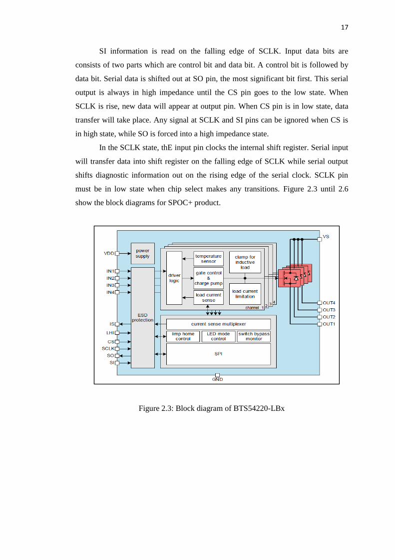
must be in low state when chip select makes any transitions. Figure 2.3 until 2.6
show the block diagrams for SPOC+ product.
Figure 2.3: Block diagram of BTS54220-LBx

18
Figure 2.4: Block diagram of BTS55032-LBx
Figure 2.5: Block diagram of BTS56033-LBx

19
Figure 2.6: Block diagram of BTS54040-LBx
2.5.2 Function of SPOC+
All the SPOC+ products have the same function where it provides protective
functions in automotive application. These devices are integrated in SMART
technology. As protective functions, it helps in reverse battery protection with
external components, short circuit protection and current limitation. Load current is
limited by the device itself where it is automatically depends on the voltage Vds
across power Diffusion Metal Oxide Semiconductor (DMOS). While for current
limitation, Internal Leakage Limit (ILLIM) is realized by increasing the resistance of
the output channel which leads to the increasing temperature inside. Besides that, it
works as loss of ground protection by securely changes to or stays in OFF-state.
Other than that, in term of diagnostic functions, the device can be enabled to
function as current sense signal configurable via SPI. It also has high accuracy of
current sense signal at wide load current range. A switch bypass monitor allows
detecting a short circuit between the output pin and the battery voltage. In terms of
applications functions, SPOC+ is one of the high side power switches for 12V

20
grounded loads in automotive applications. Special designed in SPOC+ is used for
standard exterior lightning like position light, tail light, brake light, parking light,
license plate light, indicators and equivalent LEDs. It also works as a replacement of
electromechanical relays, fuses and discrete circuits.
To meet the world-wide customer requirements for environmental friendly
products and to be compliant with government regulations, this device is available as
green products. Green product is important because of Lead-free (Pb-free) finish on
leads and suitable for Pb-free soldering according to IPC/JEDEC J-STD-020.
2.6 Final Test Concept
2.6.1 Testing Flow
In semiconductor industries, assembled devices have to go through final test before
being shipped to customer. This final test is called parametric test. Integrated circuits
are made up with smaller simple electrical components such as resistors, transistors,
diodes and capacitors. The designed was tolerated with some amount of variation in
the values of all these simple components.
Final tests in semiconductor industries include basic environmental tests to
determine resistance effects of natural elements and conditions surrounding and
electrical tests. Methods for final tests must be prepared to serve several purposes.
First, final tests must able to specify conditions that give results equivalent to the
actual service conditions. Other than that, the test must able to obtain reproducibility
of the results of the tests. Each of general tests must adaptable to a broad range of
devices by making sure the test methods are kept uniform and thus result in
conversation of equipment, resources and testing facilities. The test methods
described herein for environmental, physical, and electrical testing of devices shall
also apply, when applicable, to parts not covered by an approved military sheet-form
standard, specification sheet, or drawing.
The test methods are classified using test number and divided into five
groups. The five groups include environmental tests, mechanical characteristics test,

21
electrical characteristics, test for transistors and diodes and last but not least is
inclusive for high reliability space applications.
To test whether SPOC+ is suitable for all environments, the devices are tested
with multi temperatures. Multi temperatures include ambient, cold and warm test.
Ambient environment is classified with 25 , cold environment with -43 , and
warm test classified with 150 ,. All these temperatures were tested with range ±5
,. These ranges are suitable with the changes of temperature in handler because of
humidity.
The electrical results will vary due to normal variation in the wafer
processing. The performance of integrated circuit is considered as not meeting the
specifications when the variations exceed the design limits. Final testing is
performed by using Micro Flex tester and Delta Matrix machines. This step is
important to determine if process steps are operating within Statistical Process
control limit. The diagram in Figure 2.7 shows the process flow diagram for SPOC+
devices.
Figure 2.7: Process flow of fabricating and testing SPOC+ device
Wafer Sawing
Die Attach
Wire Bonding
A2 plating
Marking
Trim and Form
Ambient Test
Cold Test
Warm Test
Parametric
Test

22
2.6.2 Micro Flex Tester
Micro FLEX tester is one of the hardware used to test the device, it is also known as
a test head-based system. In the micro flex, it contains the electronics integrated in
the test head which includes hardware 12 instrument slots, test system computer,
power distribution panel (PDP), system monitor and controller (SMC), LA703
master clock, master support board, utility support module (USM), cooling,
Emergency Machine Off (EMO) circuit and General Purpose Input Output (GPIO)
panel. The micro FLEX can be configured with various options and instruments.
Micro Flex test system has several functions and categorized under eight
groups as follows:
• Data Transfer
• Clocks
• Pattern Synchronization
• Calibration
• Power Distribution
• Safety and Monitoring
Data transfer will distribute data to the master support board where it is
distributed to the instrument boards and the utility support module (USM). Ethernet
bus is used to communicate with the user computer network. While, LA703 will
generates the master clock for the test system and sent to the master support board,
where it is buffered and distributed to the USM and, via equal-length paths, to the
instrument boards.
Pattern generators will be kept on the instrument boards synchronized by
pattern synchronization bus. The hub for this bus is located on the master support
board. All communications to and from the pattern generators are flowed through the
hub. Calibration is important to make sure each boards is connected or disconnected
from the bus as required and to provide synchronization signal for the system users.
Power distribution system works by providing DC power to the various subsystems
and instruments in the test systems. The voltage required by the individual circuits is
handled by on-board DC-DC converters. Last but not least, safety is important in

23
each hardware. For micro flex, system monitor and control (SMC) helps to monitor
the test system. A local operating network connects to all of the instruments power
boards. The USM passes voltages to be monitored back to the SMC main board for
measurement. Figure 2.9 shows the Micro FLEX system block diagram.
Figure 2.8: Micro FLEX system block diagram
2.7 Conclusion
As summary, the literature review for this project is mainly focused on SPOC+
function and final test in production line. All the topics that have been discussed
serve as fundamental knowledge for the implementation of the project. In fact, these
topics are all related with automotive in semiconductor and improvement for SPOC+
(one of the ICs for automotive).

24
As mentioned before, the tester that will be used for SPOC+ testing
production is Micro FLEX since it is using on automatic system known with name
iTec which is capable to receive data from Camstar system. This is helpful in
production line since it helps the operator and avoid to use wrong prompt command
when the lot is started.
Ambient test removal is one of the best method to reduce cost because this
method helps to improve 30 % of the test time if compared to reducing the test time
for good and bad parts (only improve by 4 % to 10 %). However, there is a
disadvantage where more analysis are required and need two times test program
modification. However, more analysis will allow student to understand more issues
happening in the production line.
The next chapter will discuss about the methodology of the project where the
process of test program improvement and ambient test removal will be explained in
detail.