university of nairobieie.uonbi.ac.ke/sites/default/files/cae/engineering/eie/automated... ·...
TRANSCRIPT
UNIVERSITY OF NAIROBIDEPARTMENT OF ELECTRICAL AND INFORMATION ENGINEERING
FINAL YEAR PROJECT REPORT
TITLE: AUTOMATED ELECTRIC FENCEPROJECT NO.: 12
SUBMITTED BY
SAID BREK SAID
F17/23247/2008
SUPERVISOR: DR. G.N KAMUCHA
EXAMINER: DR. DHARMADHIKARY
Project report submitted in partial fulfillment of the requirements for the award of the degree ofBachelor of Science in Electrical & Electronic Engineering of the University of Nairobi.
Date of Submission: 27/04/2014
ii
DECLARATION OF ORIGINALITY
1) I understand what plagiarism is and I am aware of the university policy in this regard.
2) I declare that this final year project report is my original work and has not been submitted
elsewhere for examination, award of a degree or publication.
Where other people’s work or my own work has been used, this has properly been
acknowledged and referenced in accordance with the University of Nairobi’s requirements.
3) I have not sought or used the services of any professional agencies to produce this work.
4) I have not allowed, and shall not allow anyone to copy my work with the intention of
passing it off as his/her own work.
5) I understand that any false claim in respect of this work shall result in disciplinary action,
in accordance with University anti-plagiarism policy.
Signature: ………………………………………………………………………………………
NAME OF STUDENT: Said Brek Said
REGISTRATION NUMBER: F17/23247/2008
COLLEGE: Architecture And Engineering
FACULTY/ SCHOOL/ INSTITUTE: Engineering
DEPARTMENT: Electrical And Information Engineering
COURSE NAME: Bachelor Of Science In Electrical & Electronic Engineering
TITLE OF WORK: AUTOMATED ELECTRIC FENCE

ii
Date: ……………………………………………………………………………………………..
DEDICATION
I dedicate this work to my parents and my family in general, colleagues and friends who played asignificant role in the success I have accomplished in the completion of this project.

iii
ACKNOWLEDGEMENT
First and foremost I wish to thank the God Almighty who has seen me through my studies at the
university.
Secondly I greatly appreciate the guidance of my supervisor Dr. G. N. Kamucha, the Dean-
Faculty of Engineering, Chairman-Department of Electrical and Information Engineering and all
my lecturers and support staff at the University of Nairobi for their support which contributed
greatly to the provision of knowledge as well as the completion of this project.
Lastly, I extend special thanks to my parents, Mr. and Mrs. Brek for their mutual, emotional and
financial support throughout my education.
iv
TABLE OF CONTENTSDECLARATION OF ORIGINALITY ..................................................................................................... ii
DEDICATION............................................................................................................................................. ii
ACKNOWLEDGEMENT......................................................................................................................... iii
CHAPTER 1: INTRODUCTION..............................................................................................................1
1.1 BACKGROUND ...............................................................................................................................1
1.2 PROBLEM STATEMENT ..............................................................................................................2
1.3 OBJECTIVES ................................................................................................................................... 2
1.4 PROJECT SCOPE............................................................................................................................2
1.5 PROJECT JUSTIFICATION..........................................................................................................2
CHAPTER 2: LITERATURE REVIEW.................................................................................................. 3
2.1 INTRODUCTION.............................................................................................................................3
2.2 THE 555 TIMER IC .........................................................................................................................5
2.2.1 Description.................................................................................................................................. 5
2.2.2 Timer Circuitry ..........................................................................................................................8
2.2.3 Reset Function ............................................................................................................................9
2.2.4 Trigger Requirements................................................................................................................9
2.2.5 Control Voltage ........................................................................................................................10
2.2.6 Modes of operation...................................................................................................................11
2.3 MICROCONTROLLER ................................................................................................................13
2.3.1 Types of Microcontrollers .......................................................................................................14
2.3.2 Atmega based microcontrollers ..............................................................................................16
2.4 ARDUINO .......................................................................................................................................17
2.4.1 Arduino Software.....................................................................................................................17
2.4.2 Arduino Hardware...................................................................................................................18
2.4.2 Pulse Width Modulation..........................................................................................................19
2.5 ELECTRIC FENCE ENERGIZER ..............................................................................................19
2.5.1 Types of Energizers ...................................................................................................................20
2.6 IGNITION COIL ............................................................................................................................22
2.6.1 Principle of Operation .............................................................................................................23
2.6.2 Types of ignition coils ..............................................................................................................24
v
2.7 RELAY SWITCH ...........................................................................................................................25
2.7.1 Functions of a Relay Switch ....................................................................................................26
2.7.2 Applications of Relay ...............................................................................................................26
2.8 OP-AMP...........................................................................................................................................26
2.8.1 Circuit Notation........................................................................................................................27
2.8.2 Principle of operation ..............................................................................................................28
2.9 COMPARATOR .............................................................................................................................29
2.9.1 Principle of operation ..............................................................................................................30
2.9.2 Key Specifications ....................................................................................................................30
CHAPTER 3: DESIGN AND IMPLEMENTATION............................................................................30
3.1 DESIGN OF 555 SIREN GENERATOR......................................................................................31
3.2 DESIGN OF FENCE ENERGISER..............................................................................................32
3.2.1 Generation of PWM pulses using Arduino Uno....................................................................32
3.2.2 Generation of shock .................................................................................................................34
3.2.3 Voltage sensing comparator ....................................................................................................37
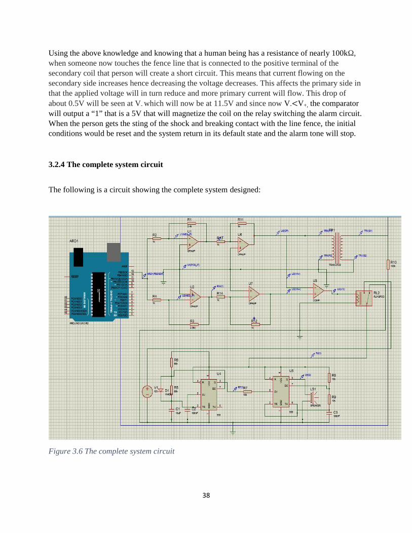
3.2.4 The complete system circuit ....................................................................................................38
CHAPTER 4: RESULTS AND ANALYSIS...........................................................................................39
4.1 Alarm circuit results .......................................................................................................................39
4.2 Shock generation circuit results.....................................................................................................40
CONCLUSION .........................................................................................................................................42
APPENDIX................................................................................................................................................42
ARDUINO SKETCH USED TO GENERATE PWM.......................................................................42
REFERENCES..........................................................................................................................................43
vi
TABLE OF FIGURESFigure 2.1 NE555 Timer ................................................................................................................. 5Figure 2.2 555 Timer Functional Block Diagram........................................................................... 6Figure 2.3 Pin-out diagram ............................................................................................................. 6Figure 2.5 Schematic of 555 Dual Timer........................................................................................ 8Figure 2.6 AC coupling of the Trigger Pulse................................................................................ 10Figure 2.7 Schematic of a 555 in monostable mode..................................................................... 11Figure 2.8 Standard 555 astable circuit......................................................................................... 12Figure 2.9 Schematic of a 555 in Bistable Mode.......................................................................... 13Figure 2.1.0 Arduino Pin Mapping ............................................................................................... 16Figure 2.11 Basic Board: Arduino Uno ........................................................................................ 18Figure 2.12 Arduino PWM signals ............................................................................................... 19Figure 2.13 Mains Energizer......................................................................................................... 20Figure 2.14 Battery Energizer....................................................................................................... 21Figure 2.15 Solar Energizer .......................................................................................................... 21Figure 2.16 Spark plug.................................................................................................................. 22Fig 2.17 Ignition coil constituents ................................................................................................ 23Figure 2.18 Types of ignition coils ............................................................................................... 25Figure 2.19 Electromagnetic or mechanical relay ........................................................................ 25Figure 2.20 Ua741 op-amp ........................................................................................................... 27Figure 2.21 Circuit diagram symbol for op-amp .......................................................................... 27Fig 2.22 An op-amp without negative feedback (a comparator) .................................................. 28Figure 2.23 An op-amp with negative feedback (a non-inverting amplifier) ............................... 28Figure 2.24 A simple op-amp comparator .................................................................................... 29Figure 3.1 555 Siren generator circuit .......................................................................................... 31Figure 3.2 Flow chart of the Arduino sketch execution process................................................... 33Figure 3.3 Generating PWM pulses and amplifying them to 12V ............................................... 34Figure 3.4 Flow chart showing the generation of shock pulses .................................................... 36Figure 3.5 Voltage comparator sensing circuit ............................................................................. 37Figure 3.6 The complete system circuit ........................................................................................ 38Figure 4.1 High frequency waveforms ......................................................................................... 39Figure 4.2 Low frequency waveforms .......................................................................................... 40Figure 4.3 Arduino Uno pin 13 PWM generated pulses............................................................... 41Figure4.4 Transformer secondary side voltage............................................................................. 42

vii
ABSTRACT
Electric fences are the most popular means of fencing since not only do they provide a physicalbarrier, they are extra effective in that they provide more security since the shock that isdelivered from the fence tends to keep both people and animal away. Over the decades, astechnology keeps on growing so as the different type of electric fences keep on emerging. So asto make my contribution in this field, this paper will cover the scope of building an automatedelectric fence which is unique in that the generation of shock and the control of an alarm systemare controlled by a micro-controller.
Currently in Kenya, it is only the top security agencies that have ventured into this kind ofelectric fencing, but their systems are more complex hence that comes at a price. What this paperwill cover is an implementation that will be affordable to all.
1
CHAPTER 1: INTRODUCTION
1.1 BACKGROUND
Electric fences began to be implemented ever since the early 1930s and they were used to control
livestock in the United States of America and New Zealand. An ignition coil of a car was used to
build the first electric fence in the year 1936-1937 by an inventor called Bill Gallagher. [1]The
electric fence is very versatile and one of its functions was in providing effective security
solutions implemented in many applications. Some of the typical installations are as listed below
a) Military bases, borders and high security installations.
b) Industrial sites and factories.
c) Remote warehouses and builders yards.
d) Cellular phone antenna sites.
e) Electricity transformer, sub-stations and electricity pylons.
f) Housing Estates.
g) Private Houses.
h) Car lots.
i) Rental storage facilities [2]
Electric fences are mostly used in agriculture. Whereas standard fences are constructed to just
form a physical barrier, electric fences are constructed to form both psychological and mental
barriers. The mental barrier is accomplished by introducing an electric shock through the fence
wire that both repels the animals and makes them less likely to contact the fence again. [3]
However in security systems, the electric shock is meant to keep intruders out and is usually
accompanied by an alarm system which is triggered when an intruder is detected and has been
shocked already. And this is what this project is aiming to achieve.

2
1.2 PROBLEM STATEMENT
Security is very essential in each home especially in these times where cases of burglary and
theft have risen off the charts. Though it is the duty of the police in our country to ensure the
safety of all citizens, it is also one’s duty to cater and make sure that his/her home is safe for the
family. This project will guide users through building a security system that isn’t complex as
such but will do the job.
1.3 OBJECTIVES
The objectives of this project is to build an automated electric fence where the generation of
shock and the alarm system are controlled by a micro-controller.
1.4 PROJECT SCOPE
This project entails the following
i. Designing an electric fence charger that is essentially a high voltage pulse generator and
linking it to the fence.
ii. Designing a 555 timer siren generator that will serve as the alarm system.
iii. Interfacing the micro-controller with the alarm system together with the necessary
arduino microcontroller program that will enable the micro-controller to execute its
function.
1.5 PROJECT JUSTIFICATION
The readily available security systems solutions in the market are very expensive. Besides the
security group of companies, the likes of G4S, KK security and Wells Fargo have completely
taken over the market and hence they tend to offer home security systems but at a ridiculously
high price. This project is hence aimed at providing a cheaper alternative of a self-built security
systems that I still as efficient as the others.
3
CHAPTER 2: LITERATURE REVIEW
2.1 INTRODUCTION
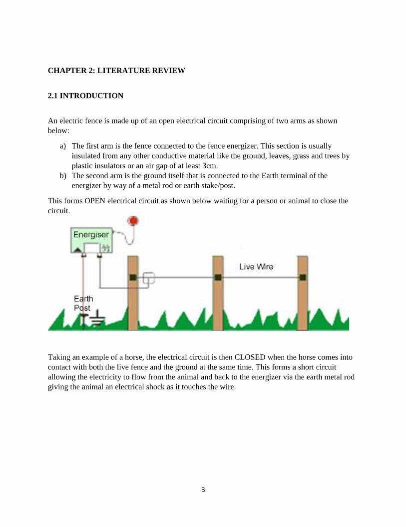
An electric fence is made up of an open electrical circuit comprising of two arms as shownbelow:
a) The first arm is the fence connected to the fence energizer. This section is usuallyinsulated from any other conductive material like the ground, leaves, grass and trees byplastic insulators or an air gap of at least 3cm.
b) The second arm is the ground itself that is connected to the Earth terminal of theenergizer by way of a metal rod or earth stake/post.
This forms OPEN electrical circuit as shown below waiting for a person or animal to close thecircuit.
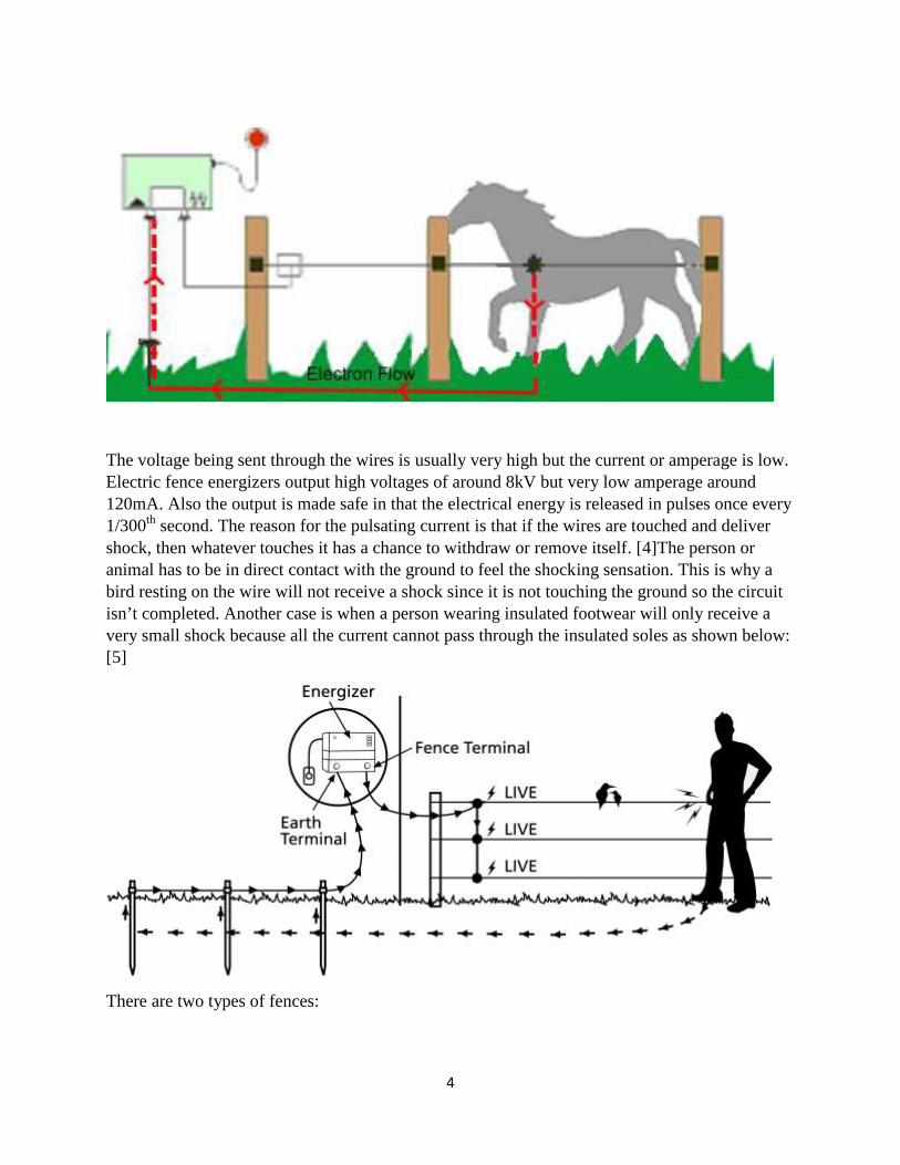
Taking an example of a horse, the electrical circuit is then CLOSED when the horse comes intocontact with both the live fence and the ground at the same time. This forms a short circuitallowing the electricity to flow from the animal and back to the energizer via the earth metal rodgiving the animal an electrical shock as it touches the wire.
4
The voltage being sent through the wires is usually very high but the current or amperage is low.Electric fence energizers output high voltages of around 8kV but very low amperage around120mA. Also the output is made safe in that the electrical energy is released in pulses once every1/300th second. The reason for the pulsating current is that if the wires are touched and delivershock, then whatever touches it has a chance to withdraw or remove itself. [4]The person oranimal has to be in direct contact with the ground to feel the shocking sensation. This is why abird resting on the wire will not receive a shock since it is not touching the ground so the circuitisn’t completed. Another case is when a person wearing insulated footwear will only receive avery small shock because all the current cannot pass through the insulated soles as shown below:[5]
There are two types of fences:

5
I. Permanent electric fences: Permanent electric fences are preferred since they provide along-term fencing solution. Compared to other fences like barbed wire, woven wire andrail fence, permanent power fence systems are economical, easy to install and operate,and require less maintenance, due to minimal physical contact with animals.
II. Temporary/Portable electric fences: Portable electric fences provide flexibility in pasturemanagement and are ideal for short-term animal control or rotational grazing. Easilytransported, constructed and maintained, portable fences are an effective temporaryfencing solution for a range of animals and situations. [5]
2.2 THE 555 TIMER IC
Philips Semiconductors introduced the 555 IC timer that was a unique functional building blockthat enjoyed unprecedented popularity. The timer’s success is mainly to several inherentcharacteristics foremost of which are; versatility, stability and low cost. The simplicity of thetimer, in conjunction with its ability to produce long time delays in a variety of applications, haslured many designers from mechanical timers, op amps, and various discrete circuits into theever increasing ranks of timer users. [7]
The 555 timer IC is an integrated circuit (chip) used in a variety of timer, pulse generation,and oscillator applications. The 555 can be also be used to provide time delays, as an oscillator,and as a flip-flop element Derivatives provide up to four timing circuits in one package. [8] Theimage below shows the NE555 timer:
Figure 2.1 NE555 Timer
2.2.1 Description
The 555 timer consists of two voltage comparators, a bistable flip-flop(R-S flip-flop), adischarge transistor, and a resistor divider network. To understand the basic concept of the timerlet’s first examine the timer in block form in Figure 1.
6
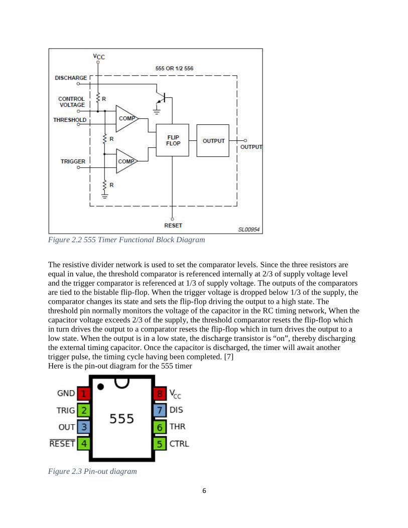
Figure 2.2 555 Timer Functional Block Diagram
The resistive divider network is used to set the comparator levels. Since the three resistors areequal in value, the threshold comparator is referenced internally at 2/3 of supply voltage leveland the trigger comparator is referenced at 1/3 of supply voltage. The outputs of the comparatorsare tied to the bistable flip-flop. When the trigger voltage is dropped below 1/3 of the supply, thecomparator changes its state and sets the flip-flop driving the output to a high state. Thethreshold pin normally monitors the voltage of the capacitor in the RC timing network, When thecapacitor voltage exceeds 2/3 of the supply, the threshold comparator resets the flip-flop whichin turn drives the output to a comparator resets the flip-flop which in turn drives the output to alow state. When the output is in a low state, the discharge transistor is “on”, thereby dischargingthe external timing capacitor. Once the capacitor is discharged, the timer will await anothertrigger pulse, the timing cycle having been completed. [7]Here is the pin-out diagram for the 555 timer
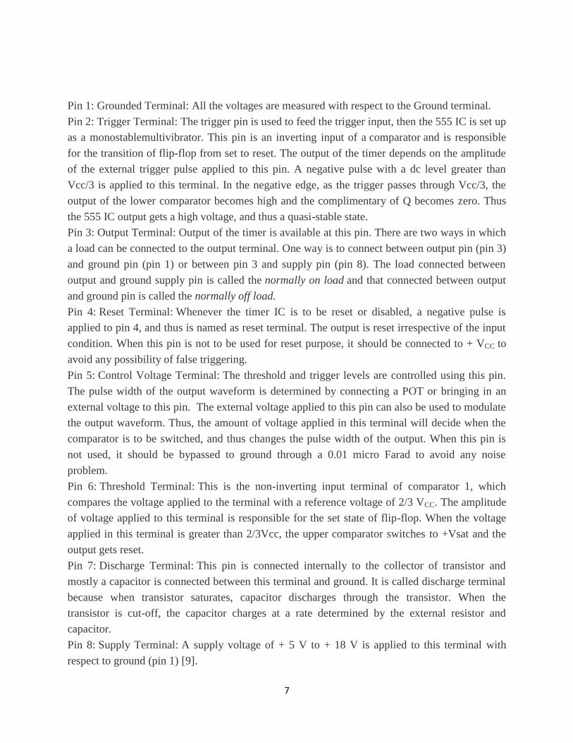
Figure 2.3 Pin-out diagram
7
Pin 1: Grounded Terminal: All the voltages are measured with respect to the Ground terminal.
Pin 2: Trigger Terminal: The trigger pin is used to feed the trigger input, then the 555 IC is set up
as a monostablemultivibrator. This pin is an inverting input of a comparator and is responsible
for the transition of flip-flop from set to reset. The output of the timer depends on the amplitude
of the external trigger pulse applied to this pin. A negative pulse with a dc level greater than
Vcc/3 is applied to this terminal. In the negative edge, as the trigger passes through Vcc/3, the
output of the lower comparator becomes high and the complimentary of Q becomes zero. Thus
the 555 IC output gets a high voltage, and thus a quasi-stable state.
Pin 3: Output Terminal: Output of the timer is available at this pin. There are two ways in which
a load can be connected to the output terminal. One way is to connect between output pin (pin 3)
and ground pin (pin 1) or between pin 3 and supply pin (pin 8). The load connected between
output and ground supply pin is called the normally on load and that connected between output
and ground pin is called the normally off load.
Pin 4: Reset Terminal: Whenever the timer IC is to be reset or disabled, a negative pulse is
applied to pin 4, and thus is named as reset terminal. The output is reset irrespective of the input
condition. When this pin is not to be used for reset purpose, it should be connected to + VCC to
avoid any possibility of false triggering.
Pin 5: Control Voltage Terminal: The threshold and trigger levels are controlled using this pin.
The pulse width of the output waveform is determined by connecting a POT or bringing in an
external voltage to this pin. The external voltage applied to this pin can also be used to modulate
the output waveform. Thus, the amount of voltage applied in this terminal will decide when the
comparator is to be switched, and thus changes the pulse width of the output. When this pin is
not used, it should be bypassed to ground through a 0.01 micro Farad to avoid any noise
problem.
Pin 6: Threshold Terminal: This is the non-inverting input terminal of comparator 1, which
compares the voltage applied to the terminal with a reference voltage of 2/3 VCC. The amplitude
of voltage applied to this terminal is responsible for the set state of flip-flop. When the voltage
applied in this terminal is greater than 2/3Vcc, the upper comparator switches to +Vsat and the
output gets reset.
Pin 7: Discharge Terminal: This pin is connected internally to the collector of transistor and
mostly a capacitor is connected between this terminal and ground. It is called discharge terminal
because when transistor saturates, capacitor discharges through the transistor. When the
transistor is cut-off, the capacitor charges at a rate determined by the external resistor and
capacitor.
Pin 8: Supply Terminal: A supply voltage of + 5 V to + 18 V is applied to this terminal with
respect to ground (pin 1) [9].
8
2.2.2 Timer Circuitry
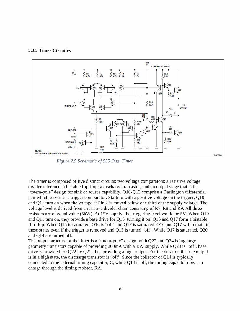
Figure 2.5 Schematic of 555 Dual Timer
The timer is composed of five distinct circuits: two voltage comparators; a resistive voltagedivider reference; a bistable flip-flop; a discharge transistor; and an output stage that is the“totem-pole” design for sink or source capability. Q10-Q13 comprise a Darlington differentialpair which serves as a trigger comparator. Starting with a positive voltage on the trigger, Q10and Q11 turn on when the voltage at Pin 2 is moved below one third of the supply voltage. Thevoltage level is derived from a resistive divider chain consisting of R7, R8 and R9. All threeresistors are of equal value (5kW). At 15V supply, the triggering level would be 5V. When Q10and Q11 turn on, they provide a base drive for Q15, turning it on. Q16 and Q17 form a bistableflip-flop. When Q15 is saturated, Q16 is “off’ and Q17 is saturated. Q16 and Q17 will remain inthese states even if the trigger is removed and Q15 is turned “off’. While Q17 is saturated, Q20and Q14 are turned off.The output structure of the timer is a “totem-pole” design, with Q22 and Q24 being largegeometry transistors capable of providing 200mA with a 15V supply. While Q20 is “off’, basedrive is provided for Q22 by Q21, thus providing a high output. For the duration that the outputis in a high state, the discharge transistor is “off’. Since the collector of Q14 is typicallyconnected to the external timing capacitor, C, while Q14 is off, the timing capacitor now cancharge through the timing resistor, RA.
9
The capacitor voltage is monitored by the threshold comparator (Q1-Q4) which is a Darlingtondifferential pair. When the capacitor voltage reaches two thirds of the supply voltage, the currentis directed from Q3 and Q4 thru Q1 and Q2. Amplification of the current change is provided byQ5 and Q6. Q5-Q6 and Q7-Q8 comprise a diode-biased amplifier. The amplified current changefrom Q6 now provides a base drive for Q16 which is part of the bistable flip-flop, to changestates. In doing so, the output is driven “low”, and Q14, the discharge transistor, is turned “on”,shorting the timing capacitor to ground.
2.2.3 Reset Function
Regressing to the trigger mode, it should be noted that once the device has triggered and thebistable flip-flop is set, continued triggering will not interfere with the timing cycle. However,there may come a time when it is necessary to interrupt or halt a timing cycle. This is thefunction that the reset accomplishes. In the normal operating mode the reset transistor, Q25, isoff with its base held high. When the base of Q25 is grounded, it turns on, providing base driveto Q14, turning it on. This discharges the timing capacitor, resets the flip-flop at Q17, and drivesthe output low. The reset overrides all other functions within the timer.
2.2.4 Trigger Requirements
Due to the nature of the trigger circuitry, the timer will trigger on the negative-going edge of theinput pulse. For the device to time-out properly, it is necessary that the trigger voltage level bereturned to some voltage greater than one third of the supply before the timeout period. This canbe achieved by making either the trigger pulse sufficiently short or by AC coupling into thetrigger. By AC coupling the trigger (see Figure 2.4), a short negative-going pulse is achievedwhen the trigger signal goes to ground. AC coupling is most frequently used in conjunction witha switch or a signal that goes to ground which initiates the timing cycle. Should the trigger beheld low, without AC coupling, for a longer duration than the timing cycle the output will remainin a high state for the duration of the low trigger signal, without regard to the thresholdcomparator state.This is due to the predominance of Q15 on the base of Q16, controlling the stateof the bistable flip-flop. When the trigger signal then returns to a high level, the output will fallimmediately. Thus, the output signal will follow the trigger signal in this case.

10
Figure 2.6 AC coupling of the Trigger Pulse
2.2.5 Control Voltage
One important thing, the control voltage, is brought out on the timer. As mentioned before, boththe trigger comparator, Q10-Q13, and the threshold comparator, Q1-Q4, are referenced to aninternal resistor divider network, R7, R8, and R9. This network establishes the nominal twothirds of supply voltage (VCC) trip point for the threshold comparator and one third of VCC forthe trigger comparator. The two thirds point at the junction of R7, R8 and the base of Q4 isbrought out. By imposing a voltage at this point, the comparator reference levels may be shiftedeither higher or lower than the nominal levels of one third and two thirds of the supply voltage.Varying the voltage at this point will vary the timing. This feature of the timer opens a multitudeof application possibilities such as using the timer as a voltage-controlled oscillator, pulse-widthmodulator, etc. For applications where the control voltage function is not used, it is stronglyrecommended that a bypass capacitor (0.01mF) be placed across the control voltage pin and
11
ground. This will increase the noise immunity of the timer to high frequency trash which maymonitor the threshold levels causing timing error.
2.2.6 Modes of operation
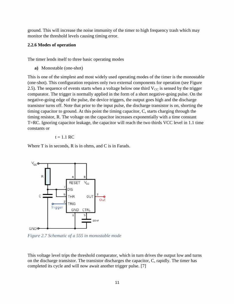
The timer lends itself to three basic operating modes
a) Monostable (one-shot)
This is one of the simplest and most widely used operating modes of the timer is the monostable(one-shot). This configuration requires only two external components for operation (see Figure2.5). The sequence of events starts when a voltage below one third VCC is sensed by the triggercomparator. The trigger is normally applied in the form of a short negative-going pulse. On thenegative-going edge of the pulse, the device triggers, the output goes high and the dischargetransistor turns off. Note that prior to the input pulse, the discharge transistor is on, shorting thetiming capacitor to ground. At this point the timing capacitor, C, starts charging through thetiming resistor, R. The voltage on the capacitor increases exponentially with a time constantT=RC. Ignoring capacitor leakage, the capacitor will reach the two thirds VCC level in 1.1 timeconstants or
t = 1.1 RC
Where T is in seconds, R is in ohms, and C is in Farads.
Figure 2.7 Schematic of a 555 in monostable mode
This voltage level trips the threshold comparator, which in turn drives the output low and turnson the discharge transistor. The transistor discharges the capacitor, C, rapidly. The timer hascompleted its cycle and will now await another trigger pulse. [7]
11
ground. This will increase the noise immunity of the timer to high frequency trash which maymonitor the threshold levels causing timing error.
2.2.6 Modes of operation
The timer lends itself to three basic operating modes
a) Monostable (one-shot)
This is one of the simplest and most widely used operating modes of the timer is the monostable(one-shot). This configuration requires only two external components for operation (see Figure2.5). The sequence of events starts when a voltage below one third VCC is sensed by the triggercomparator. The trigger is normally applied in the form of a short negative-going pulse. On thenegative-going edge of the pulse, the device triggers, the output goes high and the dischargetransistor turns off. Note that prior to the input pulse, the discharge transistor is on, shorting thetiming capacitor to ground. At this point the timing capacitor, C, starts charging through thetiming resistor, R. The voltage on the capacitor increases exponentially with a time constantT=RC. Ignoring capacitor leakage, the capacitor will reach the two thirds VCC level in 1.1 timeconstants or
t = 1.1 RC
Where T is in seconds, R is in ohms, and C is in Farads.
Figure 2.7 Schematic of a 555 in monostable mode
This voltage level trips the threshold comparator, which in turn drives the output low and turnson the discharge transistor. The transistor discharges the capacitor, C, rapidly. The timer hascompleted its cycle and will now await another trigger pulse. [7]
12
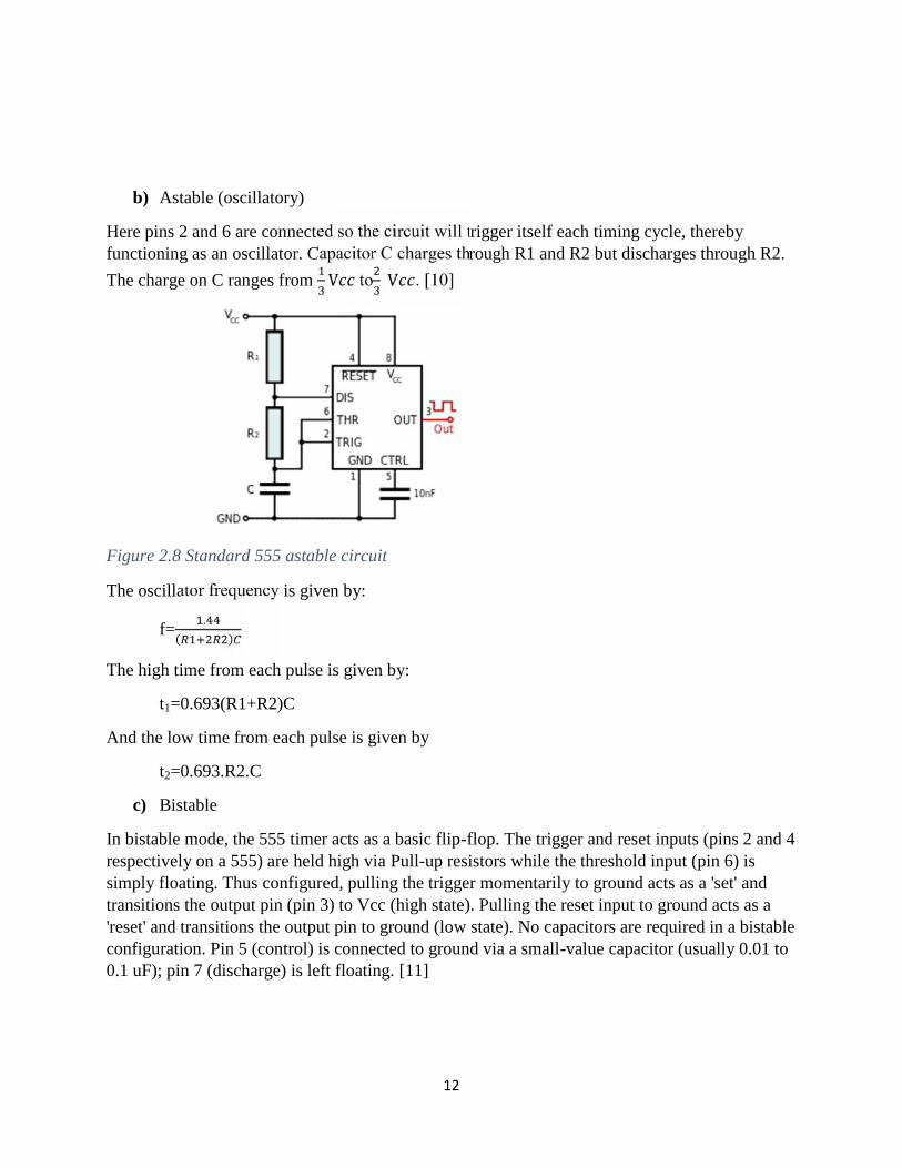
b) Astable (oscillatory)
Here pins 2 and 6 are connected so the circuit will trigger itself each timing cycle, therebyfunctioning as an oscillator. Capacitor C charges through R1 and R2 but discharges through R2.
The charge on C ranges from V to V . [10]
Figure 2.8 Standard 555 astable circuit
The oscillator frequency is given by:
f=.( )
The high time from each pulse is given by:
t1=0.693(R1+R2)C
And the low time from each pulse is given by
t2=0.693.R2.C
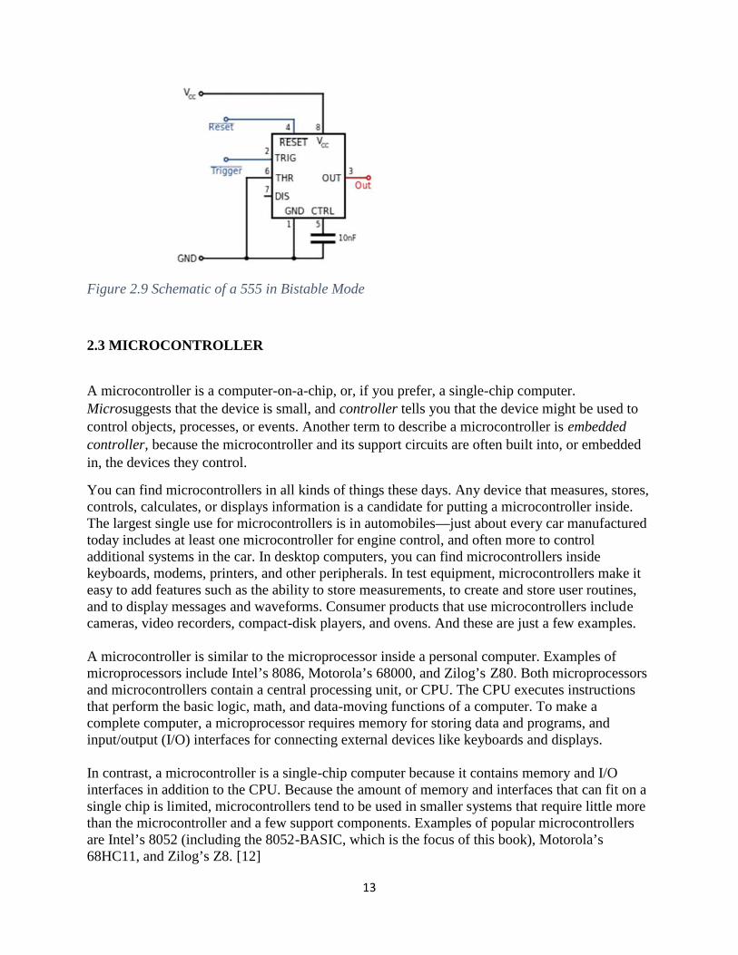
c) Bistable
In bistable mode, the 555 timer acts as a basic flip-flop. The trigger and reset inputs (pins 2 and 4respectively on a 555) are held high via Pull-up resistors while the threshold input (pin 6) issimply floating. Thus configured, pulling the trigger momentarily to ground acts as a 'set' andtransitions the output pin (pin 3) to Vcc (high state). Pulling the reset input to ground acts as a'reset' and transitions the output pin to ground (low state). No capacitors are required in a bistableconfiguration. Pin 5 (control) is connected to ground via a small-value capacitor (usually 0.01 to0.1 uF); pin 7 (discharge) is left floating. [11]
13
Figure 2.9 Schematic of a 555 in Bistable Mode
2.3 MICROCONTROLLER
A microcontroller is a computer-on-a-chip, or, if you prefer, a single-chip computer.Microsuggests that the device is small, and controller tells you that the device might be used tocontrol objects, processes, or events. Another term to describe a microcontroller is embeddedcontroller, because the microcontroller and its support circuits are often built into, or embeddedin, the devices they control.
You can find microcontrollers in all kinds of things these days. Any device that measures, stores,controls, calculates, or displays information is a candidate for putting a microcontroller inside.The largest single use for microcontrollers is in automobiles—just about every car manufacturedtoday includes at least one microcontroller for engine control, and often more to controladditional systems in the car. In desktop computers, you can find microcontrollers insidekeyboards, modems, printers, and other peripherals. In test equipment, microcontrollers make iteasy to add features such as the ability to store measurements, to create and store user routines,and to display messages and waveforms. Consumer products that use microcontrollers includecameras, video recorders, compact-disk players, and ovens. And these are just a few examples.
A microcontroller is similar to the microprocessor inside a personal computer. Examples ofmicroprocessors include Intel’s 8086, Motorola’s 68000, and Zilog’s Z80. Both microprocessorsand microcontrollers contain a central processing unit, or CPU. The CPU executes instructionsthat perform the basic logic, math, and data-moving functions of a computer. To make acomplete computer, a microprocessor requires memory for storing data and programs, andinput/output (I/O) interfaces for connecting external devices like keyboards and displays.
In contrast, a microcontroller is a single-chip computer because it contains memory and I/Ointerfaces in addition to the CPU. Because the amount of memory and interfaces that can fit on asingle chip is limited, microcontrollers tend to be used in smaller systems that require little morethan the microcontroller and a few support components. Examples of popular microcontrollersare Intel’s 8052 (including the 8052-BASIC, which is the focus of this book), Motorola’s68HC11, and Zilog’s Z8. [12]
14
2.3.1 Types of Microcontrollers
Microcontrollers can be classified according to the following
a) Number of Bits
The bits in microcontroller are 8-bits, 16-bits and 32-bits microcontroller.
In 8-bit microcontroller, the point when the internal bus is 8-bit then the ALU is performs thearithmetic and logic operations. The examples of 8-bit microcontrollers are Intel 8031/8051,PIC1x and Motorola MC68HC11 families.
The 16-bit microcontroller performs greater precision and performance as compared to 8-bit. Forexample 8 bit microcontrollers can only use 8 bits, resulting in a final range of 0×00 – 0xFF (0-255) for every cycle. In contrast, 16 bit microcontrollers with its 16 bit data width has a range of0×0000 – 0xFFFF (0-65535) for every cycle. A longer timer most extreme worth can likelyprove to be useful in certain applications and circuits. It can automatically operate on two 16 bitnumbers. Some examples of 16-bit microcontroller are 16-bit MCUs are extended 8051XA,PIC2x, Intel 8096 and Motorola MC68HC12 families.
The 32-bit microcontroller uses the 32-bit instructions to perform the arithmetic and logicoperations. These are used in automatically controlled devices including implantable medicaldevices, engine control systems, office machines, appliances and other types of embeddedsystems. Some examples are Intel/Atmel 251 family, PIC3x.
b) Memory Devices
The memory devices are divided into two types, they are
o Embedded memory microcontrollero External memory microcontroller
o Embedded memory microcontroller: When an embedded system has a microcontrollerunit that has all the functional blocks available on a chip is called an embeddedmicrocontroller. For example, 8051 having program & data memory, I/O ports, serialcommunication, counters and timers and interrupts on the chip is an embeddedmicrocontroller.
o External Memory Microcontroller: When an embedded system has a microcontroller unitthat has not all the functional blocks available on a chip is called an external memorymicrocontroller. For example, 8031 has no program memory on the chip is an externalmemory microcontroller.

15
c) Instruction set
ISC: CISC is a Complex Instruction Set Computer. It allows the programmer to use oneinstruction in place of many simpler instructions.
RISC: The RISC is stands for Reduced Instruction set Computer, this type of instruction setsreduces the design of microprocessor for industry standards. It allows each instruction to operateon any register or use any addressing mode and simultaneous access of program and data.
Example for CISC and RISC:
CISC: Mov AX, 4 RISC: Mov AX, 0
Mov BX, 2 Mov BX, 4
ADD BX, AX Mov CX, 2
Begin ADD AX, BX
Loop Begin
From above example, RISC systems shorten execution time by reducing the clock cycles perinstruction and CISC systems shorten execution time by reducing the number of instructions perprogram. The RISC gives a better execution than the CISC.
d) Memory Architecture
Memory architecture of microcontroller are two types, they are namely:
o Harvard memory architecture microcontrollero Princeton memory architecture microcontroller
Harvard Memory Architecture Microcontroller: The point when a microcontroller unit has adissimilar memory address space for the program and data memory, the microcontroller hasHarvard memory architecture in the processor.
16
Princeton Memory Architecture Microcontroller: The point when a microcontroller has acommon memory address for the program memory and data memory, the microcontroller hasPrinceton memory architecture in the processor. [13]
2.3.2 Atmega based microcontrollers
They include the atmega 8, 16, 32, 64 and 128 microcontrollers. Atmega 8 is normally a lowpower complementary metal oxide semiconductor (CMOS) 8-bit microcontroller based on theAVR enhanced RISC architecture. It is a powerful microcontroller that provides a highly flexibleand cost effective solution to many embedded control applications. The Atmega 8 AVR issupported with a full suite of program and system development tools. Furthermore, thismicrocontroller has an in-built 10-bit successive approximation ADC. Atmega 16, 32, 64 and128 microcontrollers have similar features to atmega 8 only that atmega 16, 32, 64 and 128 have16, 32, 64 and 128 bits respectively.
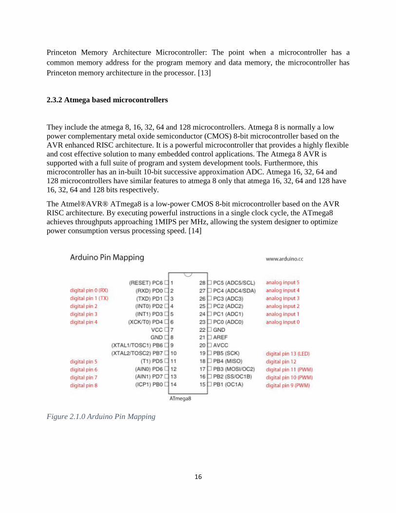
The Atmel®AVR® ATmega8 is a low-power CMOS 8-bit microcontroller based on the AVRRISC architecture. By executing powerful instructions in a single clock cycle, the ATmega8achieves throughputs approaching 1MIPS per MHz, allowing the system designer to optimizepower consumption versus processing speed. [14]
Figure 2.1.0 Arduino Pin Mapping
17
2.4 ARDUINO
Arduino is a tool for making computers that can detect and control more of the physical world
than compared to a desktop computer. It's an open-source physical computing platform based on
a simple microcontroller board, and a development environment for writing software for the
board. Arduino can be used to develop interactive objects, taking inputs from a variety of
switches and sensors, and controlling a variety of lights, motors etc. Arduino projects can be
stand-alone, or they can communicate with software running on your computer (e.g. Flash,
Processing, MaxMSP.) The boards can be assembled by hand or purchased preassembled; the
open-source IDE can be downloaded for free. The Arduino programming language is an
implementation of Wiring, a similar physical computing platform, which is based on the
Processing multimedia programming environment. [15]
The Arduino environment has been designed to be easy to use for beginners who have no
software or electronics experience. With Arduino, you can build objects that can respond to
and/or control light, sound, touch, and movement. Arduino has been used to create an amazing
variety of things, including musical instruments, robots, light sculptures, games, interactive
furniture, and even interactive clothing.
Arduino is famously known for its hardware, but you also need software to program that
hardware. Both the hardware and the software are called “Arduino.” The combination enables
you to create projects that sense and control the physical world. The software is free, open
source, and cross-platform. The boards are inexpensive to buy, or you can build your own (the
hardware designs are also open source). In addition, there is an active and supportive Arduino
community that is accessible worldwide through the Arduino forums and the wiki (known as the
Arduino Playground)
2.4.1 Arduino Software
Software programs, called sketches, are created on a computer using the Arduino integrateddevelopment environment (IDE). The IDE enables you to write and edit code and convert this
18
code into instructions that Arduino hardware understands. The IDE also transfers thoseinstructions to the Arduino board (a process called uploading).
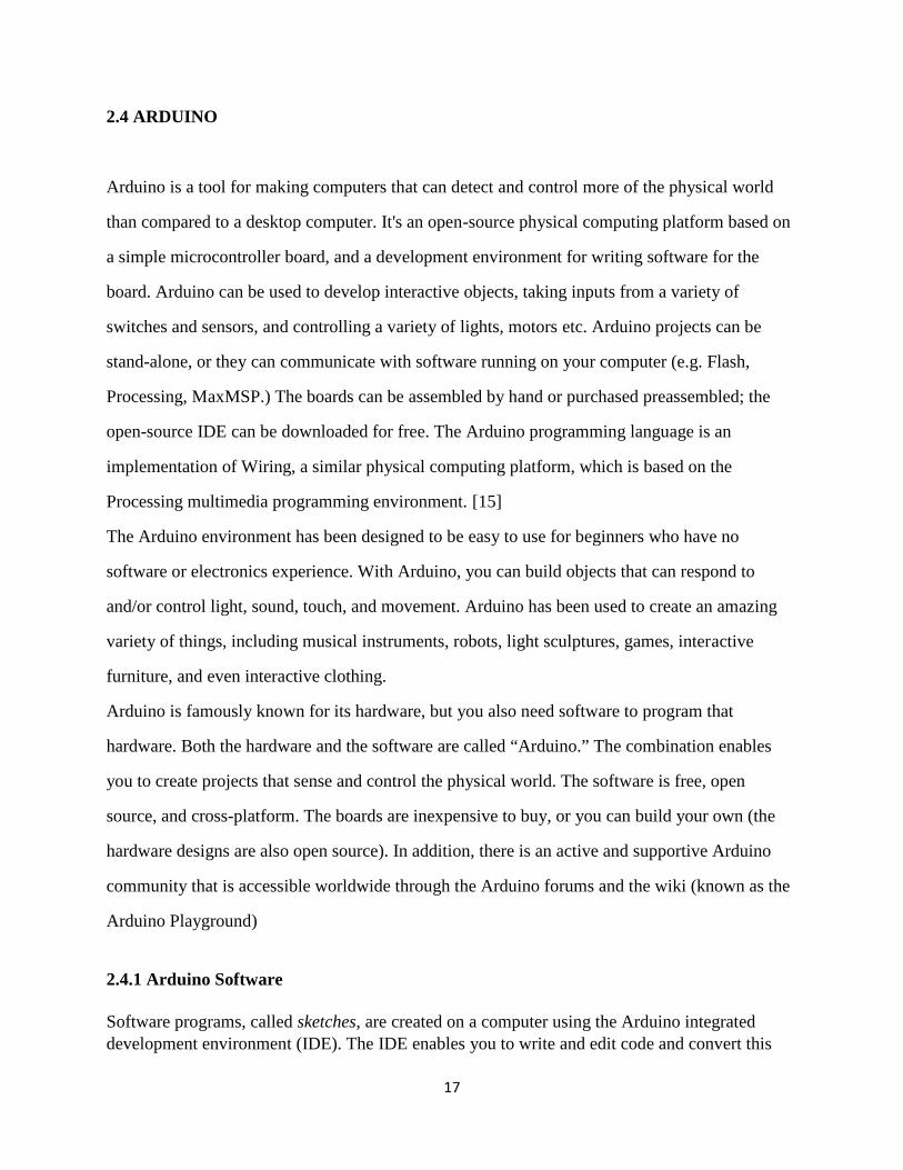
2.4.2 Arduino Hardware
The Arduino board is where the code you write is executed. The board can only control andrespond to electricity, so specific components are attached to it to enable it to interact with thereal world. These components can be sensors, which convert some aspect of the physical worldto electricity so that the board can sense it, or actuators, which get electricity from the board andconvert it into something that changes the world. Examples of sensors include switches,accelerometers, and ultrasound distance sensors. Actuators are things like lights and LEDs,speakers, motors, and displays. There are a variety of official boards that you can use withArduino software and a wide range of Arduino-compatible boards produced by members of thecommunity. The most popular boards contain a USB connector that is used to provide power andconnectivity for uploading your software onto the board. The figure 2.9 shows a basic a basicboard, the Arduino Uno [16]
Figure 2.11 Basic Board: Arduino Uno
19
2.4.2 Pulse Width Modulation
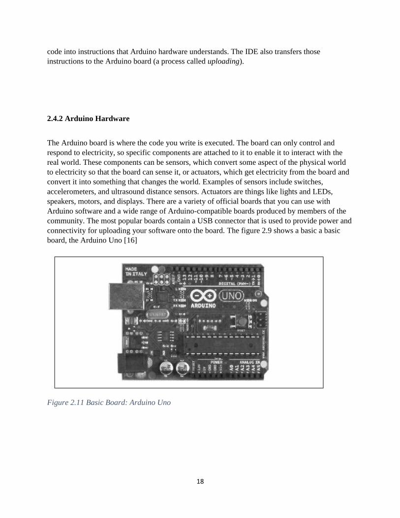
The Arduino Uno ON/HIGH/5V and OFF/LOW/0V digital outputs are termed as a square wave.The duration of the ON time is what is known as pulse-width and when the width pulse is variedrapidly to generate an effect of what seems as an analog voltage signal, then the output is termeda PWM signal. The signal looks somewhat as what is shown below: [17]
Figure 2.12 Arduino PWM signals
2.5 ELECTRIC FENCE ENERGIZER
The source of the shock in an electrical fence is the energizer. The energizer provides regularpulses of electricity to your fence. These intermittent high voltage pulses flow from theenergizer, along connection cable to the fence, and then along the length of the fence. The “live”wires of your fence should not come into contact with fence posts or corner posts, and thisachieved by the use of insulators. [17]
20
2.5.1 Types of Energizers
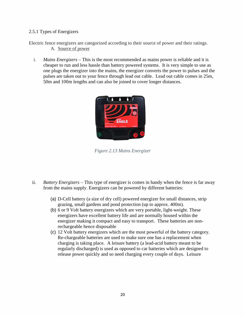
Electric fence energizers are categorized according to their source of power and their ratings.A. Source of power
i. Mains Energizers – This is the most recommended as mains power is reliable and it ischeaper to run and less hassle than battery powered systems. It is very simple to use asone plugs the energizer into the mains, the energizer converts the power to pulses and thepulses are taken out to your fence through lead out cable. Lead out cable comes in 25m,50m and 100m lengths and can also be joined to cover longer distances.
Figure 2.13 Mains Energizer
ii. Battery Energizers – This type of energizer is comes in handy when the fence is far awayfrom the mains supply. Energizers can be powered by different batteries:
(a) D-Cell battery (a size of dry cell) powered energizer for small distances, stripgrazing, small gardens and pond protection (up to approx. 400m).
(b) 6 or 9 Volt battery energizers which are very portable, light-weight. Theseenergizers have excellent battery life and are normally housed within theenergizer making it compact and easy to transport. These batteries are non-rechargeable hence disposable
(c) 12 Volt battery energizers which are the most powerful of the battery category.Re-chargeable batteries are used to make sure one has a replacement whencharging is taking place. A leisure battery (a lead-acid battery meant to beregularly discharged) is used as opposed to car batteries which are designed torelease power quickly and so need charging every couple of days. Leisure
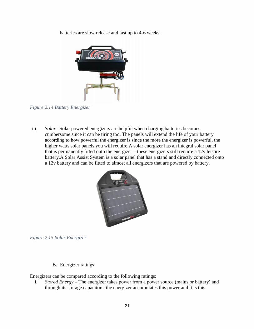
21
batteries are slow release and last up to 4-6 weeks.
Figure 2.14 Battery Energizer
iii. Solar –Solar powered energizers are helpful when charging batteries becomescumbersome since it can be tiring too. The panels will extend the life of your batteryaccording to how powerful the energizer is since the more the energizer is powerful, thehigher watts solar panels you will require.A solar energizer has an integral solar panelthat is permanently fitted onto the energizer – these energizers still require a 12v leisurebattery.A Solar Assist System is a solar panel that has a stand and directly connected ontoa 12v battery and can be fitted to almost all energizers that are powered by battery.
Figure 2.15 Solar Energizer
B. Energizer ratings
Energizers can be compared according to the following ratings:i. Stored Energy – The energizer takes power from a power source (mains or battery) and
through its storage capacitors, the energizer accumulates this power and it is this

22
energythat gives the energizer the power it creates. The amount of energy that can bestored is proportional to the length of the fence that the energizer can power.
ii. Output Energy – The energy stored in the energizer is usually discharged through an
output transformer going to the fence lines. It is inevitable that some energy is lost in this
process and hence the output energy is always lower than what was stored. This output
energy is the energy that goes down the fence and is measured in joules.
iii. Power Consumption – Depending on how powerful the energizer is, the power source
will be used accordingly. The length and type of fence is hence taken into consideration
carefully.
iv. Distance – This is estimated maximum distance the energizer will power and assumes a
suitable earth system and perfect conditions of the fence.[18]
2.6 IGNITION COIL
An ignition coil, also known as a spark coil, is an induction coil in a car’s ignition system thatsteps up the battery’s low voltage of 12V to kilovolts necessary to create an electric spark in thecar’s spark plugs to ignite the fuel. It consists of a laminated iron core enclosed by two copperwire coils but unlike a power transformer, an ignition coil has an open magnetic circuit. Thismeans that around the windings, the iron core doesn’t for a closed loop and hence the energystored in the core magnetic field is the energy that is transferred to the spark plug. [19]
Figure 2.16 Spark plug
23
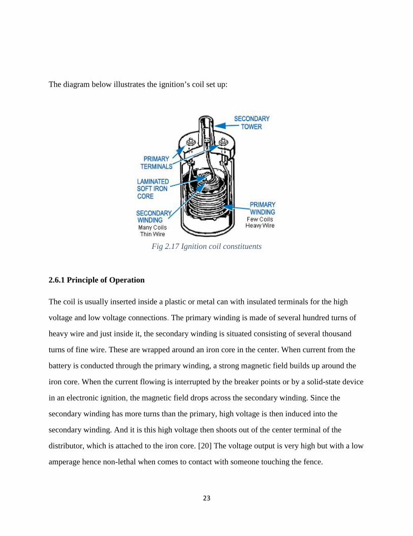
The diagram below illustrates the ignition’s coil set up:
Fig 2.17 Ignition coil constituents
2.6.1 Principle of Operation
The coil is usually inserted inside a plastic or metal can with insulated terminals for the high
voltage and low voltage connections. The primary winding is made of several hundred turns of
heavy wire and just inside it, the secondary winding is situated consisting of several thousand
turns of fine wire. These are wrapped around an iron core in the center. When current from the
battery is conducted through the primary winding, a strong magnetic field builds up around the
iron core. When the current flowing is interrupted by the breaker points or by a solid-state device
in an electronic ignition, the magnetic field drops across the secondary winding. Since the
secondary winding has more turns than the primary, high voltage is then induced into the
secondary winding. And it is this high voltage then shoots out of the center terminal of the
distributor, which is attached to the iron core. [20] The voltage output is very high but with a low
amperage hence non-lethal when comes to contact with someone touching the fence.
24
2.6.2 Types of ignition coils
Over the last few decades, car ignition technology has developed significantly and therefore,several new ignition coil types have been developed. Depending on how old a vehicle is, theengine design and the ignition system, any of the following designs of ignition coils might beused:
1. Can-type ignition coils:In older vehicles and antique cars, this type of ignition coil is what may be found to beused. Some older versions of this type are filled with oil which is to act as a coolant andalso as an insulator but most have a more modern dry insulation design.
2. Distributor coils:For this type, the induced high voltage reaches the individual spark plugs Through adistributor mechanism that is. This type is an evolution of the can-type coil and werewidely used until the 1990s.
3. Ignition blocks:Ignition blocks contain several ignition coils, which are connected by high tension cablesto each plug each. This type of ignition coil is available in single or dual sparktechnology. In single-spark ignition blocks, each of the ignition cable supplies the highvoltage pulse to one cylinder while in dual-spark blocks, the high voltage pulse is fedsimultaneously to two cylinders.
4. Pencil or coil on plug ignition coils:This ignition coil type is located directly on top of the spark plug. The high voltage pulseis taken straight to the spark plug, reducing power loss. Since pencil ignition coils arefound in the spark plug tunnel, they don’t occupy a lot of space in the enginecompartment. Pencil ignition coils are used in cars with electronic ignition systems andthey are also available as single-spark or dual-spark coils.
5. Ignition coil pack systems:So called coil packs combine a number of pencil ignition coils mounted within a singlecomponent known as a rail. This rail is then placed across a bank of several spark plugs.[21]
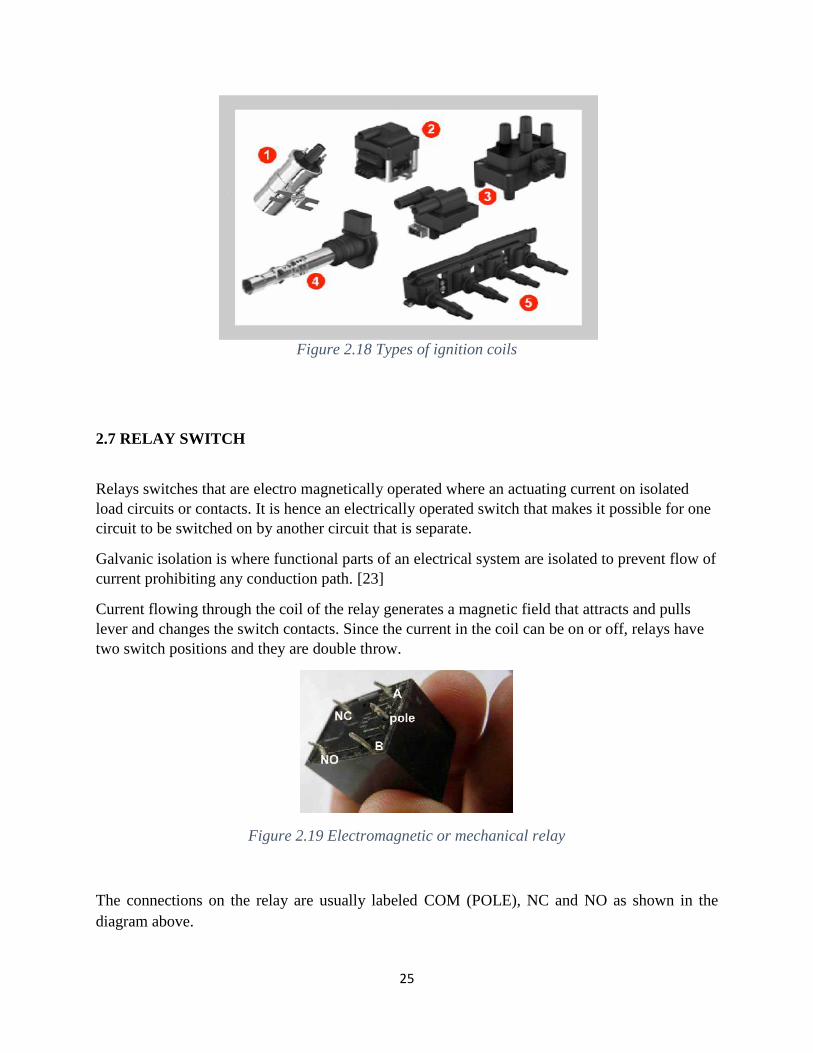
The diagram below shows all of the above 5 types of ignition coils:
25
Figure 2.18 Types of ignition coils
2.7 RELAY SWITCH
Relays switches that are electro magnetically operated where an actuating current on isolatedload circuits or contacts. It is hence an electrically operated switch that makes it possible for onecircuit to be switched on by another circuit that is separate.
Galvanic isolation is where functional parts of an electrical system are isolated to prevent flow ofcurrent prohibiting any conduction path. [23]
Current flowing through the coil of the relay generates a magnetic field that attracts and pullslever and changes the switch contacts. Since the current in the coil can be on or off, relays havetwo switch positions and they are double throw.
Figure 2.19 Electromagnetic or mechanical relay
The connections on the relay are usually labeled COM (POLE), NC and NO as shown in thediagram above.

26
COM/POLE= Common, NC and NO always connect to this, it is the moving part of the switch.
NC = Normally Closed, COM/POLE is connected to this when the relay coil is not magnetized.
NO = Normally Open, COM/POLE is connected to this when the relay coil is MAGNETIZEDand vice versa.
2.7.1 Functions of a Relay Switch
The primary functions of a relay are as follows:
a) Separating different load circuits for multi-pole relays.b) Interfacing power circuits and electronic circuits.c) It performs several switching functions e.g. delay, signal conditioning.d) Separating DC circuits from AC circuits.
2.7.2 Applications of Relay
Relays have got so many applications. The following are some of the applications:
i. Computer interfaces.ii. Air conditioning and heating.
iii. Automotive electrics.iv. Control of motors and solenoids.v. Electric power control.
vi. Production and test equipment.vii. Lighting control.
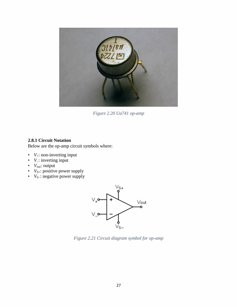
2.8 OP-AMP
An operational amplifier (op-amp) is a DC-coupled high gain electronic voltage amplifier with adifferential input and usually a single-ended output. The op-amp is a high performance linearamplifier that has a variety of uses. The op-amp has two inputs; the inverting input (-) and thenon-inverting input (+) and one output. The polarity of a signal applied to the inverting input ishence reversed at the output while when the same signal is applied to the non-inverting inputretains its polarity at the output.
27
Figure 2.20 Ua741 op-amp
2.8.1 Circuit NotationBelow are the op-amp circuit symbols where:
V+: non-inverting input V−: inverting input Vout: output VS+: positive power supply VS−: negative power supply
Figure 2.21 Circuit diagram symbol for op-amp
28
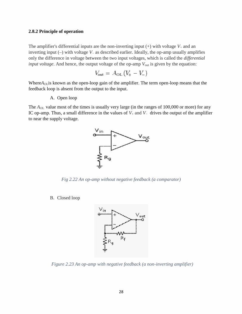
2.8.2 Principle of operation
The amplifier's differential inputs are the non-inverting input (+) with voltage V+ and aninverting input (–) with voltage V− as described earlier. Ideally, the op-amp usually amplifiesonly the difference in voltage between the two input voltages, which is called the differentialinput voltage. And hence, the output voltage of the op-amp Vout is given by the equation:
WhereAOLis known as the open-loop gain of the amplifier. The term open-loop means that thefeedback loop is absent from the output to the input.
A. Open loop
The AOL value most of the times is usually very large (in the ranges of 100,000 or more) for anyIC op-amp. Thus, a small difference in the values of V+ and V− drives the output of the amplifierto near the supply voltage.
Fig 2.22 An op-amp without negative feedback (a comparator)
B. Closed loop
Figure 2.23 An op-amp with negative feedback (a non-inverting amplifier)
28
2.8.2 Principle of operation
The amplifier's differential inputs are the non-inverting input (+) with voltage V+ and aninverting input (–) with voltage V− as described earlier. Ideally, the op-amp usually amplifiesonly the difference in voltage between the two input voltages, which is called the differentialinput voltage. And hence, the output voltage of the op-amp Vout is given by the equation:
WhereAOLis known as the open-loop gain of the amplifier. The term open-loop means that thefeedback loop is absent from the output to the input.
A. Open loop
The AOL value most of the times is usually very large (in the ranges of 100,000 or more) for anyIC op-amp. Thus, a small difference in the values of V+ and V− drives the output of the amplifierto near the supply voltage.
Fig 2.22 An op-amp without negative feedback (a comparator)
B. Closed loop
Figure 2.23 An op-amp with negative feedback (a non-inverting amplifier)

29
Negative feedback is used when a predictable operation is required. It is done by applying aportion of the output voltage back to the inverting input and the closed loop feedback greatlyreduces the circuit’s gain. Hence, when using a negative feedback the overall gain and responseof the circuit is mostly determined by the feedback network.The op-amp circuit’s response withits input, output and feedback circuits to an input is related mathematically using a transferfunction which is very important in many op-amps like in analog computers. High inputimpedance at the input terminals and the low output impedance at the output terminal are veryuseful op-amp features.
In the non-inverting amplifier given in the figure above, the presence of negative feedback viathe voltage divider Rf,Rg determines the closed loop-gain ACL = Vout / Vin. When Voutis enough topull the inverting input to equal Vin equilibrium will be. The voltage gain of the entire circuit isthus 1 + Rf/Rg. Taking for example, if Vin = 1 V and Rf = Rg, Vout will be 2 V, exactly the amountrequired to keep V− at 1 V. Because of the feedback provided by the Rf, Rg network, this is circuitis a closed loop one.
The closed-loop gain ACL is given by:
[24]
2.9 COMPARATOR
A comparator is a circuit that compares an input voltage to a given reference voltage and changesthe state of its output when the input has been exceeded. The decision-making ability is veryimportant and has many applications.
An op-amp without a feedback resistor is used to make a simple analog comparator. [25]
Figure 2.24 A simple op-amp comparator

30
2.9.1 Principle of operation
Given that the non-inverting input (V+) is at a higher voltage than the inverting input (V-), thehigh gain of the op-amp will cause the output to saturate at the highest positive voltage that it canoutput. And when the non-inverting input (V+) drops below the inverting input (V-), the outputthen saturates at the most negative voltage it can output. The op-amp's output voltage is limitedby the supply voltage. An op-amp that is operating in a linear mode with negative feedback,using a balanced, split-voltage power supply, (powered by ± VS) has its transfer functiontypically written as:
However, this equation may not be applicable to a comparator circuit which is non-linear andoperates open-loop (no negative feedback).
2.9.2 Key Specifications
Several parameters must be considered while selecting a suitable comparator:
a) Speed and power.b) Hysteresis.c) Output type.d) Internal reference. [26]
CHAPTER 3: DESIGN AND IMPLEMENTATION
The electric fence energizer to be designed is unique in that generation of shock is to becontrolled using a microcontroller where it generates PWM pulses of 5V magnitude and sendsthem to an ignition coil that steps the pulses to around 12KV. This method of generating pulsesis advantageous in that the micro-controller generates accurate pulses.
The system consists of three parts namely:
31
i. Alarm system(555 siren generator).ii. Generation of shock.
iii. Voltage sensing comparator.
3.1 DESIGN OF 555 SIREN GENERATOR
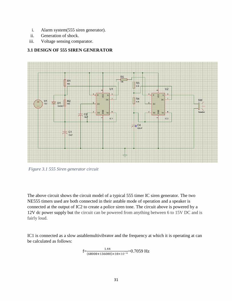
Figure 3.1 555 Siren generator circuit
The above circuit shows the circuit model of a typical 555 timer IC siren generator. The twoNE555 timers used are both connected in their astable mode of operation and a speaker isconnected at the output of IC2 to create a police siren tone. The circuit above is powered by a12V dc power supply but the circuit can be powered from anything between 6 to 15V DC and isfairly loud.
IC1 is connected as a slow astablemultivibrator and the frequency at which it is operating at canbe calculated as follows:
f=.( )× × =0.7059 Hz
32
The diode between pins 6 and 7 of IC1 functions to allow current only in its forward directionhence this makes the current to flow only in one direction so that the pulse generated will bereduced to half. This is to say that the duty cycle will be set to 50%.
IC2 is then connected as a fast astablemultivibrators operating at high frequencies of:
f= .( )× × =480 Hz
The output of IC1 is then connected to the control voltage pin (pin 5) of IC2 and in doing so, theoutput of IC2 is modulated by the frequency of IC1. It is this modulating effect that gives thesiren effect.
A speaker is then connected out of IC2 pin 3so as to produce the siren sound. The loudness of thesiren can be further increased by connecting a power amplifier then to the speaker.
3.2 DESIGN OF FENCE ENERGISER
The fence energizer consists of an Arduino board whose microcontroller generates PWM pulsesand an ignition coil that will step up the generated pulses to kilovolts. These pulses are thenoutput from the positive terminal of the secondary side of the ignition coil and to the fence whichwill give a painful but non-lethal sensation when touched by either a person or an animal.
3.2.1 Generation of PWM pulses using Arduino Uno
The advantage of the Arduino’s programming language is that it makes PWM very easy toimplement by simply calling analogWrite (pin, dutyCycle), where dutyCycle is usually a valuefrom 0 to 255 since the Atmega328 is an 8 bit microcontroller. Pin is one of the PWM pins (3, 5,6, 10, 11). The analogWrite gives a simple interface to the hardware PWM but it isdisadvantageous in that it doesn’t provide any control frequency.
It is due to this that I will proceed to generate PWM pulses using the bit-banging method. Whatthis means is that you can “manually” implement PWM on any pin repeatedly by turning the pinON and OFF for the desired times.
Choosing pins 10 and 13 on the Arduino board to output the required PWM pulses, a sketch ofthe program will be provided at the end of this report specifically in the Appendix section. Pinsgenerated from pin 10 serve as signals to the inverting input of a comparator for voltagecomparison functionality as will be discussed late or while pulses from pin 13 will be taken tothe ignition coil for stepping up. However, the following is a flow chart illustrating how it goesabout to generate the pulses:
33
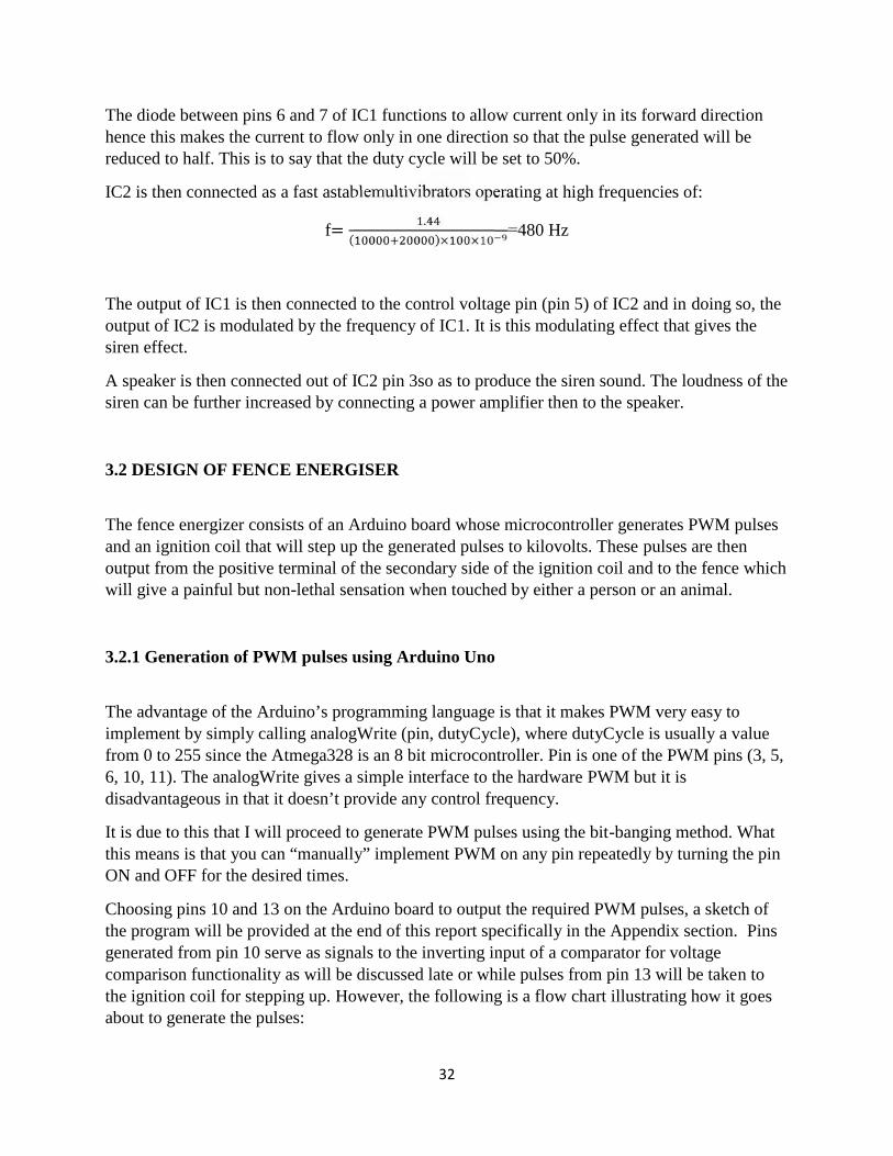
Figure 3.2 Flow chart of the Arduino sketch execution process
The generated PWM pulses will be of 5V value, they will have to be amplified to near values of12V before going to the ignition coil for stepping up purposes. Operational amplifiers, op-amps,were implemented to amplify these pulses.
Start
Take Pin 13to HIGH
(5V)
Wait for 2milliseconds
Set pin 13 toLOW (0V)
Wait for 18milliseconds

34
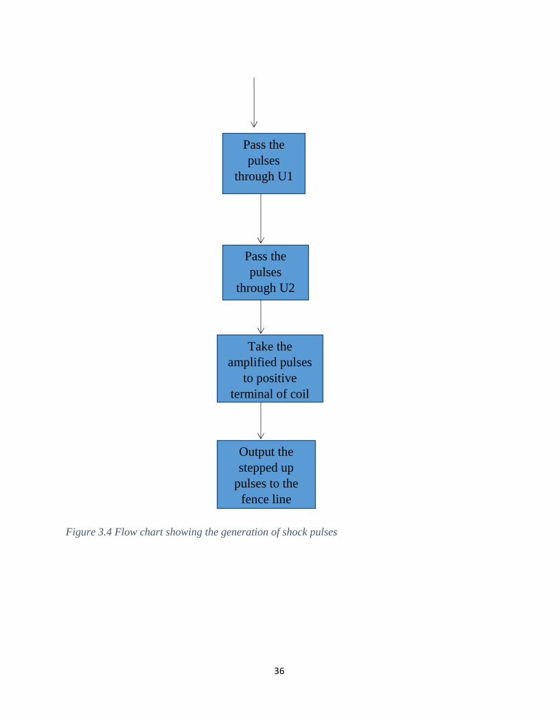
3.2.2 Generation of shock
Figure 3.3 Generating PWM pulses and amplifying them to 12V
Pulses from the digital pin 13 of the Arduino are at 5V and passing them through the first op-amp U1 amplifies it. Since the op-amp is connected as an inverting amplifier, the gain supplied isa negative gain. The voltage output is calculated as follows:
= − ×= −2.4 × 101 × 10 × 5 = −12
35
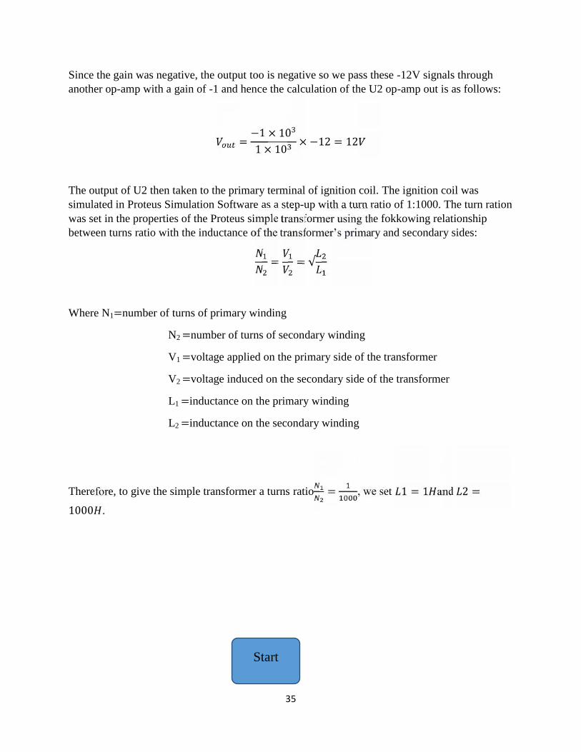
Since the gain was negative, the output too is negative so we pass these -12V signals throughanother op-amp with a gain of -1 and hence the calculation of the U2 op-amp out is as follows:
= −1 × 101 × 10 × −12 = 12The output of U2 then taken to the primary terminal of ignition coil. The ignition coil wassimulated in Proteus Simulation Software as a step-up with a turn ratio of 1:1000. The turn rationwas set in the properties of the Proteus simple transformer using the fokkowing relationshipbetween turns ratio with the inductance of the transformer’s primary and secondary sides:= = √Where N1=number of turns of primary winding
N2=number of turns of secondary winding
V1=voltage applied on the primary side of the transformer
V2=voltage induced on the secondary side of the transformer
L1=inductance on the primary winding
L2=inductance on the secondary winding
Therefore, to give the simple transformer a turns ratio = , we set 1 = 1 and 2 =1000 .
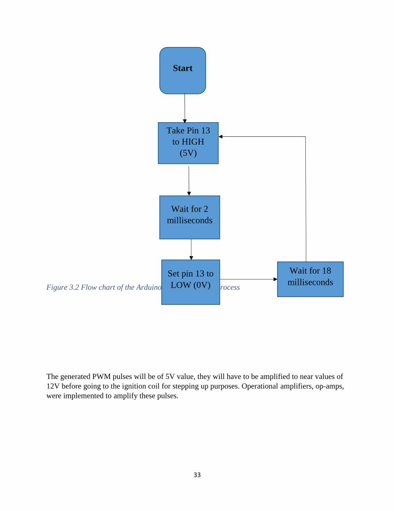
Start
36
Figure 3.4 Flow chart showing the generation of shock pulses
Pass thepulses
through U1
Pass thepulses
through U2
Take theamplified pulses
to positiveterminal of coil
Output thestepped up
pulses to thefence line
37
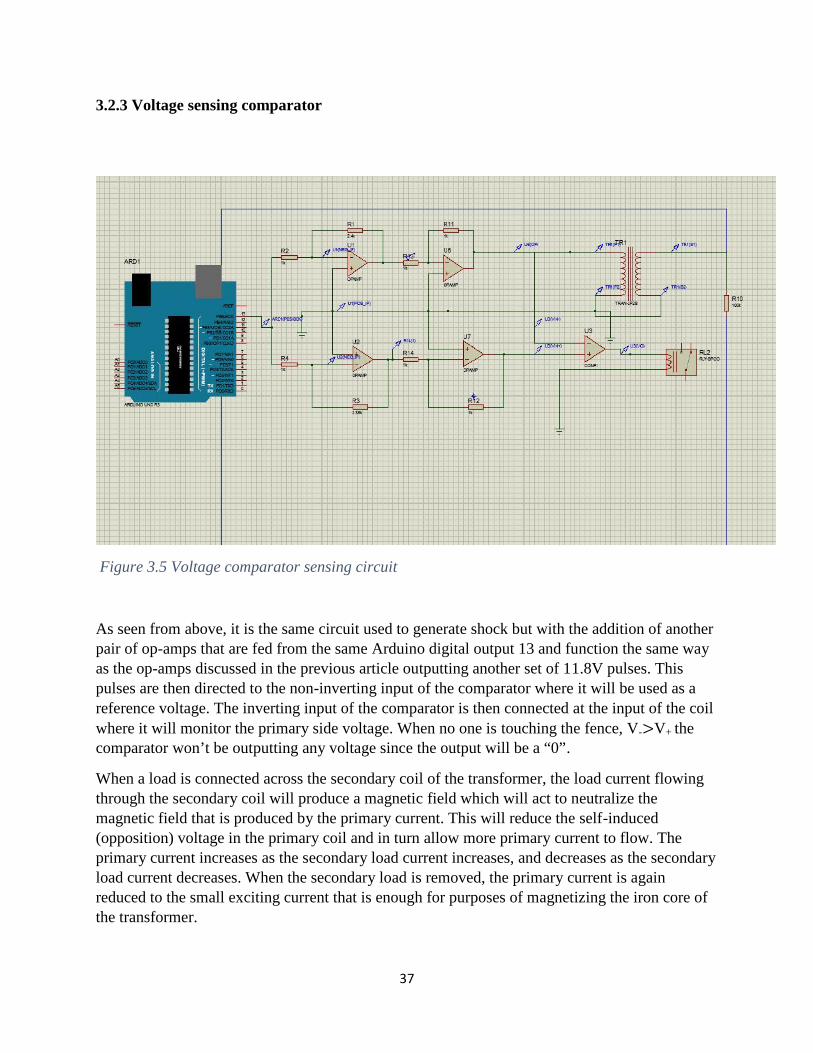
3.2.3 Voltage sensing comparator
Figure 3.5 Voltage comparator sensing circuit
As seen from above, it is the same circuit used to generate shock but with the addition of anotherpair of op-amps that are fed from the same Arduino digital output 13 and function the same wayas the op-amps discussed in the previous article outputting another set of 11.8V pulses. Thispulses are then directed to the non-inverting input of the comparator where it will be used as areference voltage. The inverting input of the comparator is then connected at the input of the coilwhere it will monitor the primary side voltage. When no one is touching the fence, V->V+ thecomparator won’t be outputting any voltage since the output will be a “0”.
When a load is connected across the secondary coil of the transformer, the load current flowingthrough the secondary coil will produce a magnetic field which will act to neutralize themagnetic field that is produced by the primary current. This will reduce the self-induced(opposition) voltage in the primary coil and in turn allow more primary current to flow. Theprimary current increases as the secondary load current increases, and decreases as the secondaryload current decreases. When the secondary load is removed, the primary current is againreduced to the small exciting current that is enough for purposes of magnetizing the iron core ofthe transformer.
38
Using the above knowledge and knowing that a human being has a resistance of nearly 100kΩ,when someone now touches the fence line that is connected to the positive terminal of thesecondary coil that person will create a short circuit. This means that current flowing on thesecondary side increases hence decreasing the voltage decreases. This affects the primary side inthat the applied voltage will in turn reduce and more primary current will flow. This drop ofabout 0.5V will be seen at V- which will now be at 11.5V and since now V-<V+, the comparatorwill output a “1” that is a 5V that will magnetize the coil on the relay switching the alarm circuit.When the person gets the sting of the shock and breaking contact with the line fence, the initialconditions would be reset and the system return in its default state and the alarm tone will stop.
3.2.4 The complete system circuit
The following is a circuit showing the complete system designed:
Figure 3.6 The complete system circuit

39
CHAPTER 4: RESULTS AND ANALYSIS
4.1 Alarm circuit results
The following waveforms were obtained from the output of the second 555 timer in the alarmcircuit:
Figure 4.1 High frequency waveforms
Period=1 millisecond = 1 = 11 × 10 = 1000Vpeak = 2V

40
Figure 4.2 Low frequency waveforms
Period = 2 millisecond = 12 × 10 = 500The above two waveforms of high and low frequencies from the second and first ICsrespectively indicate the siren like sound output at the speaker for the alarm.
4.2 Shock generation circuit results
The Arduino digital pin 13 output of PWM pulses were captured in the simulation software:
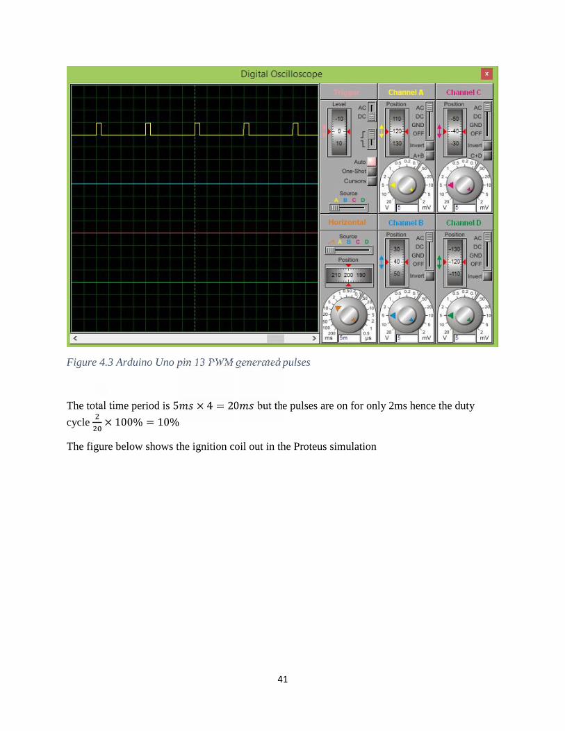
41
Figure 4.3 Arduino Uno pin 13 PWM generated pulses
The total time period is 5 × 4 = 20 but the pulses are on for only 2ms hence the duty
cycle × 100% = 10%The figure below shows the ignition coil out in the Proteus simulation
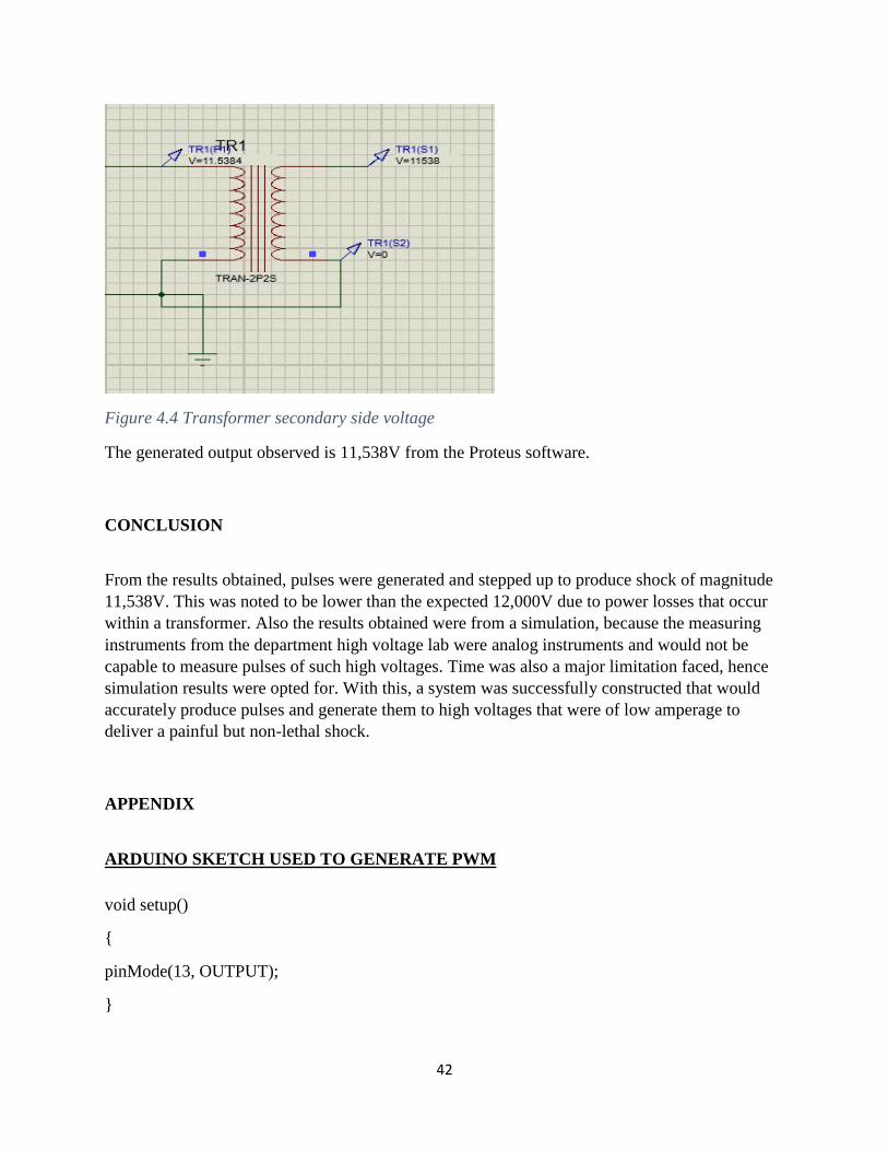
42
Figure 4.4 Transformer secondary side voltage
The generated output observed is 11,538V from the Proteus software.
CONCLUSION
From the results obtained, pulses were generated and stepped up to produce shock of magnitude11,538V. This was noted to be lower than the expected 12,000V due to power losses that occurwithin a transformer. Also the results obtained were from a simulation, because the measuringinstruments from the department high voltage lab were analog instruments and would not becapable to measure pulses of such high voltages. Time was also a major limitation faced, hencesimulation results were opted for. With this, a system was successfully constructed that wouldaccurately produce pulses and generate them to high voltages that were of low amperage todeliver a painful but non-lethal shock.
APPENDIX
ARDUINO SKETCH USED TO GENERATE PWM
void setup()
{
pinMode(13, OUTPUT);
}
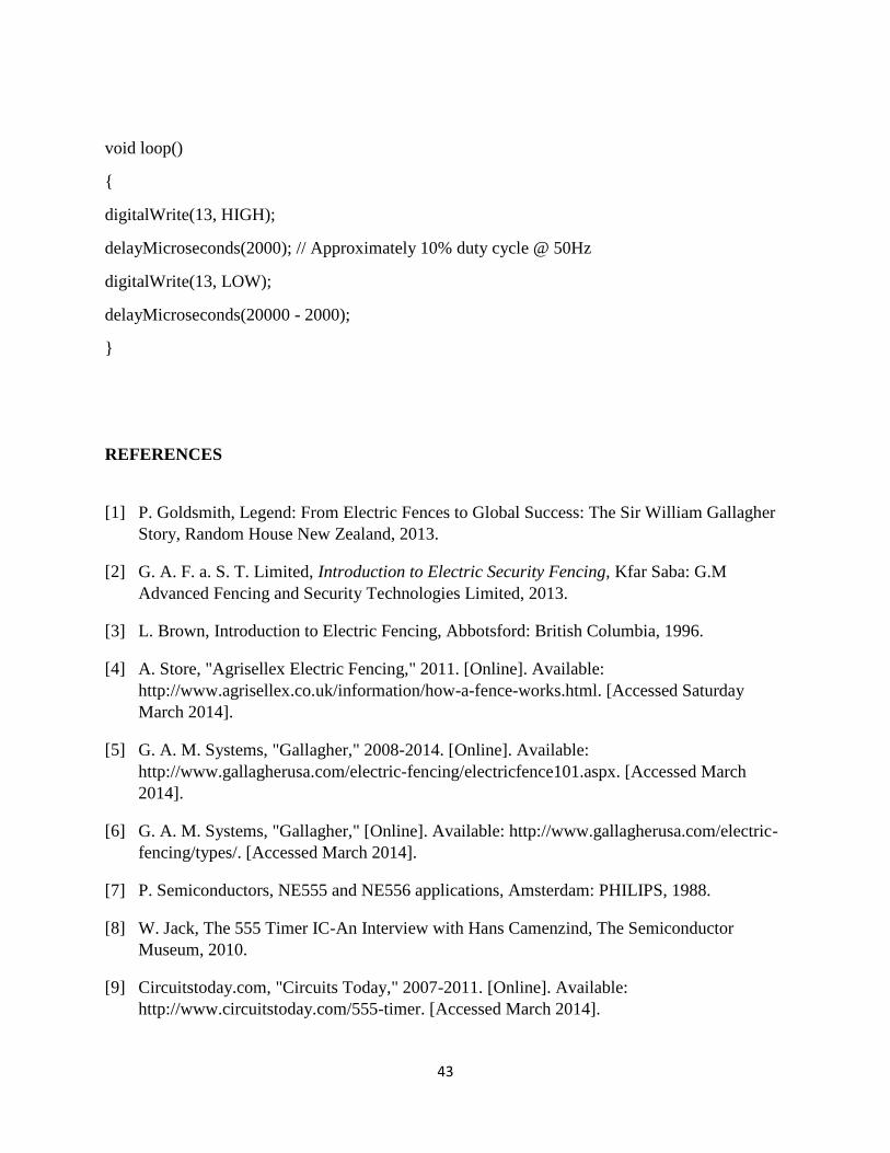
43
void loop()
{
digitalWrite(13, HIGH);
delayMicroseconds(2000); // Approximately 10% duty cycle @ 50Hz
digitalWrite(13, LOW);
delayMicroseconds(20000 - 2000);
}
REFERENCES
[1] P. Goldsmith, Legend: From Electric Fences to Global Success: The Sir William GallagherStory, Random House New Zealand, 2013.
[2] G. A. F. a. S. T. Limited, Introduction to Electric Security Fencing, Kfar Saba: G.MAdvanced Fencing and Security Technologies Limited, 2013.
[3] L. Brown, Introduction to Electric Fencing, Abbotsford: British Columbia, 1996.
[4] A. Store, "Agrisellex Electric Fencing," 2011. [Online]. Available:http://www.agrisellex.co.uk/information/how-a-fence-works.html. [Accessed SaturdayMarch 2014].
[5] G. A. M. Systems, "Gallagher," 2008-2014. [Online]. Available:http://www.gallagherusa.com/electric-fencing/electricfence101.aspx. [Accessed March2014].
[6] G. A. M. Systems, "Gallagher," [Online]. Available: http://www.gallagherusa.com/electric-fencing/types/. [Accessed March 2014].
[7] P. Semiconductors, NE555 and NE556 applications, Amsterdam: PHILIPS, 1988.
[8] W. Jack, The 555 Timer IC-An Interview with Hans Camenzind, The SemiconductorMuseum, 2010.
[9] Circuitstoday.com, "Circuits Today," 2007-2011. [Online]. Available:http://www.circuitstoday.com/555-timer. [Accessed March 2014].
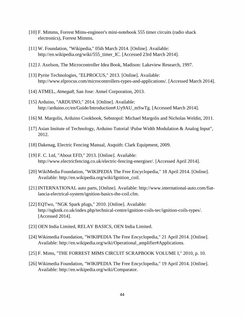
44
[10] F. Mimms, Forrest Mims-engineer's mini-notebook 555 timer circuits (radio shackelectronics), Forrest Mimms.
[11] W. Foundation, "Wikipedia," 05th March 2014. [Online]. Available:http://en.wikipedia.org/wiki/555_timer_IC. [Accessed 23rd March 2014].
[12] J. Axelson, The Microcontroller Idea Book, Madison: Lakeview Research, 1997.
[13] Pyrite Technologies, "ELPROCUS," 2013. [Online]. Available:http://www.elprocus.com/microcontrollers-types-and-applications/. [Accessed March 2014].
[14] ATMEL, Atmega8, San Jose: Atmel Corporation, 2013.
[15] Arduino, "ARDUINO," 2014. [Online]. Available:http://arduino.cc/en/Guide/Introduction#.Uy9AU_mSwTg. [Accessed March 2014].
[16] M. Margolis, Arduino Cookbook, Sebstopol: Michael Margolis and Nicholas Weldin, 2011.
[17] Asian Insitute of Technology, Arduino Tutorial \Pulse Width Modulation & Analog Input",2012.
[18] Dakenag, Electric Fencing Manual, Asquith: Clark Equipment, 2009.
[19] F. C. Ltd, "About EFD," 2013. [Online]. Available:http://www.electricfencing.co.uk/electric-fencing-energiser/. [Accessed April 2014].
[20] WikiMedia Foundation, "WIKIPEDIA The Free Encyclopedia," 18 April 2014. [Online].Available: http://en.wikipedia.org/wiki/Ignition_coil.
[21] INTERNATIONAL auto parts, [Online]. Available: http://www.international-auto.com/fiat-lancia-electrical-system/ignition-basics-the-coil.cfm.
[22] EQTwo, "NGK Spark plugs," 2010. [Online]. Available:http://ngkntk.co.uk/index.php/technical-centre/ignition-coils-tec/ignition-coils-types/.[Accessed 2014].
[23] OEN India Limited, RELAY BASICS, OEN India Limited.
[24] Wikimedia Foundation, "WIKIPEDIA The Free Encyclopedia," 21 April 2014. [Online].Available: http://en.wikipedia.org/wiki/Operational_amplifier#Applications.
[25] F. Mims, "THE FORREST MIMS CIRCUIT SCRAPBOOK VOLUME I," 2010, p. 10.
[26] Wikimedia Foundation, "WIKIPEDIA The Free Encyclopedia," 19 April 2014. [Online].Available: http://en.wikipedia.org/wiki/Comparator.

45