upd360 datasheet - microchip technologyww1.microchip.com/downloads/en/devicedoc/00002084c.pdf ·...
TRANSCRIPT
UPD360Highly Integrated Small Form Factor
USB Type-C™ Power Delivery 2.0 Port Controller
Highlights
• Small Form Factor 4 x 4 mm 44-WFBGA Package
• Integrated Analog Discrete Components Reduce Bill of Materials and Design Footprint
• USB Power Delivery 2.0 Compliant MAC
• USB Type-CTM (1) Connector Support with Connection Detection and Control
• I2C/SPI (2) Interface for CPU/SoC Communication
• USB Type-C™ Alternate Mode Support
• Dual Role Power (DRP) and Role Swap Support
Target Applications
• Notebook Computers
• All-in-One/Desktop PCs
• Smartphones
• Tablets
• Monitors
• Docking Stations
• HDTVs
• Printers
Key Benefits
• Integrated Analog Discrete Components
- VCONN FETs with Rp/Rd Switching
- Dead Battery Rd termination
- Programmable Current Sense for Overcurrent Conditions
- Voltage Sense for Overvoltage Conditions
• Integrated 5V/3A Port Power Controller (PPC)
- Supports up to 5V/3A on VBUS
- Supplies 500mA, 900mA, 1.5A, and 3.0A per USB Type-C™ Specification
• Integrated 3.3V Power Switch
- Provides Dead Battery Support
- Automatically Switch between VBUS and Main +3.3V
• USB Power Delivery MAC
- Compliant with USB Power Delivery Specification Revision 2.0
- Power Delivery Packet Framing
- CRC Checking/Generation
- 4B/5B Encoding/Decoding
- BMC Encoding/Decoding
- EOP/SOP Generation for PD Frames
- SOP Detection and SOP Header Processing
- Separate RX/TX FIFOs
- Automatic GoodCRC Message Generation
- Automatic Retry Generation
- Error Handling
- Low Standby Power Support via Sleep State
• USB Type-C Cable Detect Logic
- Auto Cable Attach & Orientation Detection
- Routes Baseband Communication to Respective CC Pin per Detected Orientation
- VCONN Supply Control for Active Cable
- Configurable Downstream Facing Port (DFP) and Upstream Facing Port (UFP) Modes
- Charging Current Capability Detection
- Detection of Debug Accessory Mode, Audio Adapter Accessory Mode
• +1.8V I2C (1 MHz) Interface Supports Communi-cation/Configuration via Companion CPU/SoC
• Alternate Mode Support
- DisplayPortTM, ThunderboltTM, and other Major Protocols
• CFG_SEL0 Pin for Selection of Device Mode
• CFG_SEL1 Pin for Selection of I2C addresses (2)
• Power and I/Os
- Integrated 1.8V Voltage Regulator
- 16 Configurable General Purpose I/O Pins
• Software
- C Libraries
• Package
- 44-ball WFBGA (4 x 4 x 0.7 mm)
• Environmental
- Commercial Temperature Range (0°C to +70°C)
1. USB Type-C™ and USB-C™ are trademarks ofUSB Implementers Forum.
2. Available only in select UPD360 configurations.
2016-2017 Microchip Technology Inc. DS00002084C-page 1
UPD360
TO OUR VALUED CUSTOMERS
It is our intention to provide our valued customers with the best documentation possible to ensure successful use of your Microchipproducts. To this end, we will continue to improve our publications to better suit your needs. Our publications will be refined andenhanced as new volumes and updates are introduced.
If you have any questions or comments regarding this publication, please contact the Marketing Communications Department viaE-mail at [email protected]. We welcome your feedback.
Most Current DocumentationTo obtain the most up-to-date version of this documentation, please register at our Worldwide Web site at:
http://www.microchip.com
You can determine the version of a data sheet by examining its literature number found on the bottom outside corner of any page. The last character of the literature number is the version number, (e.g., DS30000000A is version A of document DS30000000).
ErrataAn errata sheet, describing minor operational differences from the data sheet and recommended workarounds, may exist for cur-rent devices. As device/documentation issues become known to us, we will publish an errata sheet. The errata will specify therevision of silicon and revision of document to which it applies.
To determine if an errata sheet exists for a particular device, please check with one of the following:• Microchip’s Worldwide Web site; http://www.microchip.com• Your local Microchip sales office (see last page)
When contacting a sales office, please specify which device, revision of silicon and data sheet (include -literature number) you areusing.
Customer Notification SystemRegister on our web site at www.microchip.com to receive the most current information on all of our products.
DS00002084C-page 2 2016-2017 Microchip Technology Inc.

2016-2017 Microchip Technology Inc. DS00002084C-page 3
UPD360
Table of Contents
1.0 Preface ............................................................................................................................................................................................ 42.0 Introduction ..................................................................................................................................................................................... 73.0 Ball Descriptions and Configuration ................................................................................................................................................ 94.0 Register Map ................................................................................................................................................................................. 195.0 I2C Slave Controller (UPD360-A/UPD360-B Only) ....................................................................................................................... 206.0 SPI Slave Controller (UPD360-C Only) ........................................................................................................................................ 267.0 Clocks, Resets, and Power Management ..................................................................................................................................... 318.0 System Control ............................................................................................................................................................................. 359.0 Cable Plug Orientation and Detection ........................................................................................................................................... 6810.0 Baseband CC Interface (BCI) ................................................................................................................................................... 10711.0 Power Delivery MAC ................................................................................................................................................................. 11112.0 USB Port Power Controller (PPC) ............................................................................................................................................ 17113.0 Power Switch ............................................................................................................................................................................ 18214.0 DisplayPort Hot Plug Detect (HPD) .......................................................................................................................................... 19515.0 Watchdog Timer (WDT) ............................................................................................................................................................ 20216.0 Operational Characteristics ....................................................................................................................................................... 20617.0 Package Information ................................................................................................................................................................. 214Appendix A: Data Sheet Revision History ......................................................................................................................................... 217The Microchip Web Site .................................................................................................................................................................... 218Customer Change Notification Service ............................................................................................................................................. 218Customer Support ............................................................................................................................................................................. 218Product Identification System ........................................................................................................................................................... 219

UPD360
1.0 PREFACE
1.1 Glossary of Terms
TABLE 1-1: GLOSSARY OF TERMS
Term Definition
ADC Analog to Digital Converter
AFE Analog Front End
BCI Baseband CC Interface
Billboard USB Billboard Device. A required USB device class for UFPs which support Alternate Modes in order to provide product information to the USB Host.
BIST Built-In Self Test
BMC Bi-phase Mark Coding
Byte 8-bits
CC Generic reference to USB Type-C™ Cable / Connector CC1/CC2 pins
CSR Control and Status Register
DB Dead Battery
DFP Downstream Facing Port (USB Type-C™ Specification definition)
DP DisplayPort (a VESA standard interface)
DPM Device Policy Manager (PD Specification definition)
DRP Dual Role Power (USB Type-C™ Specification definition)
DWORD 32-bits
EC Embedded Controller
EP USB Endpoint
FIFO First In First Out buffer
FW Firmware
FS Full-Speed
Host External system (Includes processor, application software, etc.)
HPD Hot-Plug Detect functionality as defined by DisplayPort and DisplayPort Alternate Mode speci-fications
HS High-Speed
HW Hardware (Refers to function implemented by the device)
IC Integrated Circuit
IFC InterFrame Gap
LDO Linear Drop-Out regulator
MAC Media Access Controller
Microchip Microchip Technology Incorporated
N/A Not Applicable
OCS Over-Current Sense
PCS Physical Coding Sublayer
PD / UPD USB Power Delivery
PIO General Purpose I/O
PMIC Power Management Integrated Circuit
POR Power-On Reset
PRBS Pseudo Random Binary Sequence
QWORD 64-bits
SA Source Address
DS00002084C-page 4 2016-2017 Microchip Technology Inc.
UPD360
1.2 Buffer Types
SBU SideBand Use
SCSR System Control and Status Register
SPM System Policy Manager (PD Specification definition)
SS SuperSpeed
SVDM Standard/Vendor Defined Message (PD Specification definition)
SVID Standard/Vendor IDentity (PD Specification definition)
TCPC USB Type-C™ Port Controller
UFP Upstream Facing Port (USB Type-C™ Specification definition)
USB Universal Serial Bus
USB Type-C™ USB Type-C™ Cable / Connector
VDO Vendor-defined Object (PD Specification definition)
VSM Vendor Specific Messaging
WORD 16-bits
ZLP Zero Length USB Packet
TABLE 1-2: BUFFER TYPES
Buffer Type Description
IS Schmitt-triggered input
I2C I2C interface
O8 Output with 8 mA sink and 8 mA source
OD8 Open-drain output with 8 mA sink
PU 70k (typical) internal pull-up. Unless otherwise noted in the pin description, internal pull-ups are always enabled.
Note: Internal pull-up resistors prevent unconnected inputs from floating. Do not rely oninternal resistors to drive signals external to the device. When connected to a loadthat must be pulled high, an external resistor must be added.
PD 70k (typical) internal pull-down. Unless otherwise noted in the pin description, internal pull-downs are always enabled.
Note: Internal pull-down resistors prevent unconnected inputs from floating. Do not relyon internal resistors to drive signals external to the device. When connected to aload that must be pulled low, an external resistor must be added.
AIO Analog bidirectional
P Power pin
Note: Digital signals are not 5V tolerant unless specified.
Note: Refer to Section 16.5, "DC Characteristics," on page 208 for the electrical characteristics of the various buf-fers.
TABLE 1-1: GLOSSARY OF TERMS (CONTINUED)
Term Definition
2016-2017 Microchip Technology Inc. DS00002084C-page 5
UPD360
1.3 Register Nomenclature
1.4 References
• NXP I2C-Bus Specification (UM10204, April 4, 2014): www.nxp.com/documents/user_manual/UM10204.pdf
• USB Power Delivery and USB Type-C™ Specifications: http://www.usb.org/developers/docs/usb_31_102015.zip
• VESA DisplayPort Alternate Mode Specification 1.0: http://www.vesa.org
TABLE 1-3: REGISTER NOMENCLATURE
Register Bit Type Notation Register Bit Description
R Read: A register or bit with this attribute can be read.
W Write: A register or bit with this attribute can be written.
RO Read only: Read only. Writes have no effect.
RS Read to Set: This bit is set on read.
WO Write only: If a register or bit is write-only, reads will return unspecified data.
W1S Write One to Set: Writing a one sets the value. Writing a zero has no effect.
W1C Write One to Clear: Writing a one clears the value. Writing a zero has no effect.
WC Write Anything to Clear: Writing anything clears the value.
LL Latch Low: Clear on read of register.
LH Latch High: Clear on read of register.
SC Self-Clearing: Contents are self-cleared after the being set. Writes of zero have no effect. Contents can be read.
RO/LH Read Only, Latch High: Bits with this attribute will stay high until the bit is read. After it is read, the bit will remain high, but will change to low if the condition that caused the bit to go high is removed. If the bit has not been read, the bit will remain high regard-less of a change to the high condition.
NASR Not Affected by Software Reset. The state of NASR bits do not change on assertion of a software reset.
RESERVED Reserved Field: Reserved fields must be written with zeros, unless otherwise indi-cated, to ensure future compatibility. The value of reserved bits is not guaranteed on a read.
DS00002084C-page 6 2016-2017 Microchip Technology Inc.
UPD360
2.0 INTRODUCTION
2.1 General Description
The UPD360 is a highly integrated, small form factor USB Type-C Power Delivery (PD) Port Controller designed toadhere to the USB Type-C™ Cable and Connector Specification and USB Power Delivery 2.0 Specification. TheUPD360 provides cable plug orientation and detection for a USB Type-C receptacle and implements baseband commu-nication with a partner USB Type-C device via the integrated USB Power Delivery 2.0 MAC. The device can function inStandalone UFP/DFP modes, or utilize the integrated I2C/SPI interface to connect to a companion CPU/SoC (depen-dent on device version, see Section 2.2, "UPD360 Family Differences Summary").
Additionally, the UPD360 integrates many of the analog discrete components required for USB Type-C PD applications,including two VCONN FETs with Rp/Rd switching, a port power controller that supports up to 5V/3A on VBUS, and cur-rent and voltage sense circuitry for over-voltage/current detection. By integrating many of the analog discrete compo-nents required for USB Type-C PD applications, the UPD360 provides a low cost, low power, small footprint (4 x 4 mm)solution for consumer (notebooks, desktop PCs, smartphones, tablets, monitors, docking stations) applications.
To enable the UPD360 to efficiently support dead battery use cases, an integrated power switch is provided to selectbetween two external 3.3V supplies (VBUS and main). This effectively allows connection detection and system wakeupwithout external processor intervention (external processor in sleep mode).
The UPD360 is also capable of negotiating alternate modes over USB Type-C connectors using the Power Delivery 2.0protocol. Both DisplayPort and Thunderbolt operation over USB Type-C connectors are supported in addition to othermajor protocols.
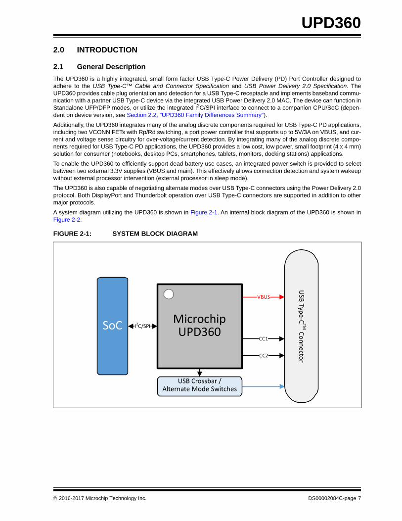
A system diagram utilizing the UPD360 is shown in Figure 2-1. An internal block diagram of the UPD360 is shown inFigure 2-2.
FIGURE 2-1: SYSTEM BLOCK DIAGRAM
MicrochipUPD360
USB
Type‐C
TMConn
ector
VBUS
CC1
CC2
SoC I2C/SPI
USB Crossbar /Alternate Mode Switches
2016-2017 Microchip Technology Inc. DS00002084C-page 7

UPD360
2.2 UPD360 Family Differences Summary
The UPD360 is available in three versions:
• UPD360-A
• UPD360-B
• UPD360-C
A summary of the differences between these versions is provided in Table 2-1. Device specific features that do no per-tain to the entire UPD360 family are called out independently throughout this document. For ordering information, referto the Product Identification System on page 219.
FIGURE 2-2: INTERNAL BLOCK DIAGRAM
TABLE 2-1: UPD360 FAMILY DIFFERENCES
Device +1.8V I2C Interface +3.3V I2C Interface SPI Interface Standalone UFP/DFP Mode
UPD360-A X X
UPD360-B X X
UPD360-C X
UPD360
3V3_ALW
Rp‐Low
Rd
Rp‐High
Rp‐Low
Rd
BasebandCC
Interface
VCONN(5V)
VCONN(5V)
AutoPowerSwitch
3V3_VBUS
1.8V LDO Regulator
VSW
CC1
CC2
5V/3APort Power
Controller
VBUS
I2CController(UPD360‐A: +1.8V)(UPD360‐B: +3.3V)
GPIOs(16x)
OCS_COMP1
Over‐CurrentDetectionOCS_COMP2
I2C(UPD360‐A/B Only)
Rp‐High
Mux
Mux
Mux
Mux
FETFET
SPIController
(UPD360‐C Only)
SPI(UPD360‐C Only)
PowerDelivery
2.0MAC
GPIO[0:15](GPIO0 not available in UPD360‐C)
DS00002084C-page 8 2016-2017 Microchip Technology Inc.

UPD360
3.0 BALL DESCRIPTIONS AND CONFIGURATION
3.1 Ball Assignments
The ball assignments for the UPD360-A/UPD360-B are detailed in Section 3.1.1, "UPD360-A/UPD360-B Ball Assign-ments," on page 9. The ball assignments for the UPD360-C are detailed in Section 3.1.1, "UPD360-A/UPD360-B BallAssignments," on page 9. For information on the differences between the UPD360 family of devices, refer to Section2.2, "UPD360 Family Differences Summary," on page 8.
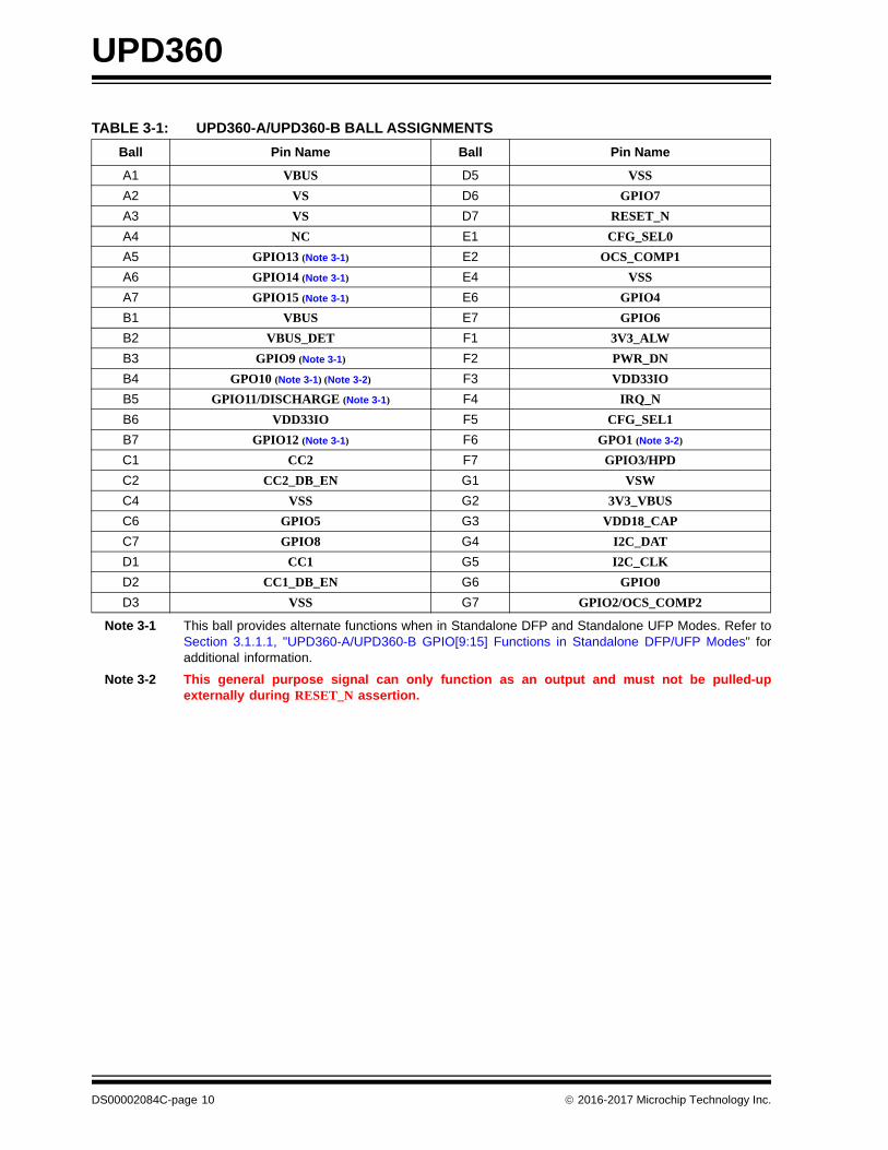
3.1.1 UPD360-A/UPD360-B BALL ASSIGNMENTS
The device ball diagram for the UPD360-A/UPD360-B can be seen in Figure 3-1. Table 3-1 provides a UPD360-A/UPD360-B ball assignment table. Ball descriptions are provided in Section 3.2, "Ball Descriptions".
FIGURE 3-1: UPD360-A/UPD360-B BALL ASSIGNMENTS (TOP VIEW)
VBUS
VBUS
CC2
CC1
CFG_SEL 0
Top of UPD360-A/UPD360-B 44-WFBGA Package
A
B
C
D
E
1 2 3 4 5 6
VS
VBUS_DET
CC2_DB_EN
CC1_DB_EN
OCS_COMP1
VS
GPIO9*
VSS
NC
GPO10*
VSS
VSS
GPIO13*
GPIO11*/DISCHARGE
VSS
GPIO 14*
VDD33IO
GPIO5
GPIO7
GPIO4
7
GPIO15*
GPIO12*
GPIO 8
RESET_N
GPIO 6
3V3_ALW
VSW
F
G
PWR_DN
3V3_VBUS
VDD33IO
VDD18_CAP
IRQ_N
I2C_DAT
CFG_SEL 1
I2C_CLK
GPO1
GPIO0
GPIO3/HPD
GPIO 2/OCS_COMP2
*The GPIO[9:15] balls provide alternate functions when in Standalone DFP or Standalone UFP modes.
2016-2017 Microchip Technology Inc. DS00002084C-page 9
UPD360
Note 3-1 This ball provides alternate functions when in Standalone DFP and Standalone UFP Modes. Refer toSection 3.1.1.1, "UPD360-A/UPD360-B GPIO[9:15] Functions in Standalone DFP/UFP Modes" foradditional information.
Note 3-2 This general purpose signal can only function as an output and must not be pulled-upexternally during RESET_N assertion.
TABLE 3-1: UPD360-A/UPD360-B BALL ASSIGNMENTS
Ball Pin Name Ball Pin Name
A1 VBUS D5 VSS
A2 VS D6 GPIO7
A3 VS D7 RESET_N
A4 NC E1 CFG_SEL0
A5 GPIO13 (Note 3-1) E2 OCS_COMP1
A6 GPIO14 (Note 3-1) E4 VSS
A7 GPIO15 (Note 3-1) E6 GPIO4
B1 VBUS E7 GPIO6
B2 VBUS_DET F1 3V3_ALW
B3 GPIO9 (Note 3-1) F2 PWR_DN
B4 GPO10 (Note 3-1) (Note 3-2) F3 VDD33IO
B5 GPIO11/DISCHARGE (Note 3-1) F4 IRQ_N
B6 VDD33IO F5 CFG_SEL1
B7 GPIO12 (Note 3-1) F6 GPO1 (Note 3-2)
C1 CC2 F7 GPIO3/HPD
C2 CC2_DB_EN G1 VSW
C4 VSS G2 3V3_VBUS
C6 GPIO5 G3 VDD18_CAP
C7 GPIO8 G4 I2C_DAT
D1 CC1 G5 I2C_CLK
D2 CC1_DB_EN G6 GPIO0
D3 VSS G7 GPIO2/OCS_COMP2
DS00002084C-page 10 2016-2017 Microchip Technology Inc.
UPD360
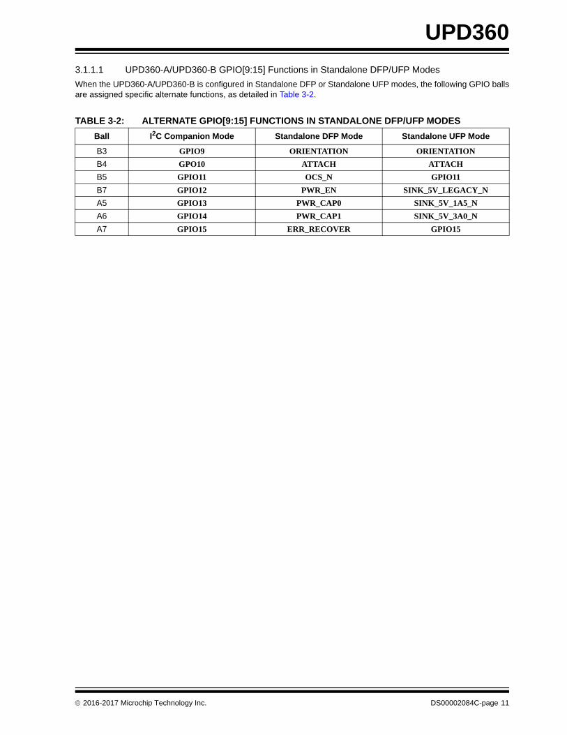
3.1.1.1 UPD360-A/UPD360-B GPIO[9:15] Functions in Standalone DFP/UFP Modes
When the UPD360-A/UPD360-B is configured in Standalone DFP or Standalone UFP modes, the following GPIO ballsare assigned specific alternate functions, as detailed in Table 3-2.
TABLE 3-2: ALTERNATE GPIO[9:15] FUNCTIONS IN STANDALONE DFP/UFP MODES
Ball I2C Companion Mode Standalone DFP Mode Standalone UFP Mode
B3 GPIO9 ORIENTATION ORIENTATION
B4 GPO10 ATTACH ATTACH
B5 GPIO11 OCS_N GPIO11
B7 GPIO12 PWR_EN SINK_5V_LEGACY_N
A5 GPIO13 PWR_CAP0 SINK_5V_1A5_N
A6 GPIO14 PWR_CAP1 SINK_5V_3A0_N
A7 GPIO15 ERR_RECOVER GPIO15
2016-2017 Microchip Technology Inc. DS00002084C-page 11
UPD360
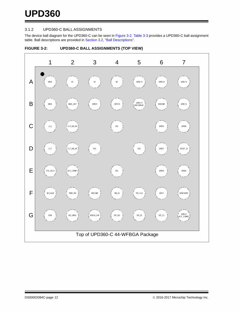
3.1.2 UPD360-C BALL ASSIGNMENTS
The device ball diagram for the UPD360-C can be seen in Figure 3-2. Table 3-3 provides a UPD360-C ball assignmenttable. Ball descriptions are provided in Section 3.2, "Ball Descriptions".
FIGURE 3-2: UPD360-C BALL ASSIGNMENTS (TOP VIEW)
VBUS
VBUS
CC2
CC1
CFG_SEL 0
Top of UPD360-C 44-WFBGA Package
A
B
C
D
E
1 2 3 4 5 6
VS
VBUS_DET
CC2_DB_EN
CC1_DB_EN
OCS_COMP1
VS
GPIO 9
VSS
NC
GPO10
VSS
VSS
GPIO 13
GPIO11/DISCHARGE
VSS
GPIO14
VDD33IO
GPIO5
GPIO7
GPIO4
7
GPIO 15
GPIO 12
GPIO8
RESET _N
GPIO6
3V3_ALW
VSW
F
G
PWR_DN
3V3_VBUS
VDD33IO
VDD18_CAP
IRQ_N
SPI _DO
SPI_CLK
SPI_DI
GPO1
SPI_CS
GPIO3/HPD
GPIO 2/OCS_COMP2
DS00002084C-page 12 2016-2017 Microchip Technology Inc.

UPD360
Note 3-3 This general purpose signal can only function as an output and must not be pulled-upexternally during RESET_N assertion.
TABLE 3-3: UPD360-C BALL ASSIGNMENTS
Ball Pin Name Ball Pin Name
A1 VBUS D5 VSS
A2 VS D6 GPIO7
A3 VS D7 RESET_N
A4 NC E1 CFG_SEL0
A5 GPIO13 E2 OCS_COMP1
A6 GPIO14 E4 VSS
A7 GPIO15 E6 GPIO4
B1 VBUS E7 GPIO6
B2 VBUS_DET F1 3V3_ALW
B3 GPIO9 F2 PWR_DN
B4 GPO10 (Note 3-3) F3 VDD33IO
B5 GPIO11/DISCHARGE F4 IRQ_N
B6 VDD33IO F5 SPI_CLK
B7 GPIO12 F6 GPO1 (Note 3-3)
C1 CC2 F7 GPIO3/HPD
C2 CC2_DB_EN G1 VSW
C4 VSS G2 3V3_VBUS
C6 GPIO5 G3 VDD18_CAP
C7 GPIO8 G4 SPI_DO
D1 CC1 G5 SPI_DI
D2 CC1_DB_EN G6 SPI_CS
D3 VSS G7 GPIO2/OCS_COMP2
2016-2017 Microchip Technology Inc. DS00002084C-page 13
UPD360
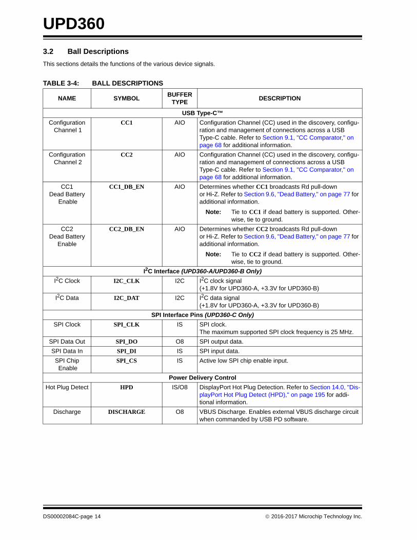
3.2 Ball Descriptions
This sections details the functions of the various device signals.
TABLE 3-4: BALL DESCRIPTIONS
NAME SYMBOLBUFFER
TYPEDESCRIPTION
USB Type-C™
Configuration Channel 1
CC1 AIO Configuration Channel (CC) used in the discovery, configu-ration and management of connections across a USB Type-C cable. Refer to Section 9.1, "CC Comparator," on page 68 for additional information.
Configuration Channel 2
CC2 AIO Configuration Channel (CC) used in the discovery, configu-ration and management of connections across a USB Type-C cable. Refer to Section 9.1, "CC Comparator," on page 68 for additional information.
CC1Dead Battery
Enable
CC1_DB_EN AIO Determines whether CC1 broadcasts Rd pull-down or Hi-Z. Refer to Section 9.6, "Dead Battery," on page 77 for additional information.
Note: Tie to CC1 if dead battery is supported. Other-wise, tie to ground.
CC2Dead Battery
Enable
CC2_DB_EN AIO Determines whether CC2 broadcasts Rd pull-down or Hi-Z. Refer to Section 9.6, "Dead Battery," on page 77 for additional information.
Note: Tie to CC2 if dead battery is supported. Other-wise, tie to ground.
I2C Interface (UPD360-A/UPD360-B Only)
I2C Clock I2C_CLK I2C I2C clock signal (+1.8V for UPD360-A, +3.3V for UPD360-B)
I2C Data I2C_DAT I2C I2C data signal(+1.8V for UPD360-A, +3.3V for UPD360-B)
SPI Interface Pins (UPD360-C Only)
SPI Clock SPI_CLK IS SPI clock.The maximum supported SPI clock frequency is 25 MHz.
SPI Data Out SPI_DO O8 SPI output data.
SPI Data In SPI_DI IS SPI input data.
SPI Chip Enable
SPI_CS IS Active low SPI chip enable input.
Power Delivery Control
Hot Plug Detect HPD IS/O8 DisplayPort Hot Plug Detection. Refer to Section 14.0, "Dis-playPort Hot Plug Detect (HPD)," on page 195 for addi-tional information.
Discharge DISCHARGE O8 VBUS Discharge. Enables external VBUS discharge circuit when commanded by USB PD software.
DS00002084C-page 14 2016-2017 Microchip Technology Inc.

UPD360
Type-CAttach
ATTACH O8 In the Standalone UFP and Standalone DFP modes (UPD360-A/UPD360-B only), this signal indicates that the USB Type-C receptacles at the near and far end of the cable both have a plug-in. This pin is autonomously driven by the device in DFP standalone mode.
0b: Nothing attached1b: USB Type-C port has an end-end attached
Refer to Section 9.10, "Standalone DFP (UPD360-A/UPD360-B Only)" and Section 9.11, "Standalone UFP (UPD360-A/UPD360-B Only)"for additional information.
Note: Float this signal when unused.
Note: This signal is not available in the UPD360-C.
Type-COrientation
ORIENTATION O8 In the Standalone UFP and Standalone DFP modes (UPD360-A/UPD360-B only), this signal is used to indicate which CC pin is terminated by the attached DFP/UFP and is autonomously driven by the device in DFP standalone mode.
DFP:0b: CC1 pin is terminated by Rd.1b: CC2 pin is terminated by Rd.
UFP:0b: CC1 pin is pulled to a higher voltage than CC2.1b: CC2 pin is pulled to a higher voltage than CC1.
Refer to Section 9.10, "Standalone DFP (UPD360-A/UPD360-B Only)" and Section 9.11, "Standalone UFP (UPD360-A/UPD360-B Only)"for additional information.
Note: Float this signal when unused.
Note: This signal is not available in the UPD360-C.
Over-current sense
OCS_N OD8 In the Standalone DFP mode (UPD360-A/UPD360-B only), this active-low signal indicates over-current sense. This sig-nal maps to the PPC_INT interrupt.
Note: This signal is active-low. Float this signal whenunused.
Note: This signal is not available in the UPD360-C.
VBUS Power Enable
PWR_EN IS In the Standalone DFP mode (UPD360-A/UPD360-B only), this signal is used as a port power switch enable for USB hubs.
Note: This signal should be tied to the Power Goodsignal from the VS supply.
Note: Tie this signal to ground when unused.
Note: This signal is not available in the UPD360-C.
TABLE 3-4: BALL DESCRIPTIONS (CONTINUED)
NAME SYMBOLBUFFER
TYPEDESCRIPTION
2016-2017 Microchip Technology Inc. DS00002084C-page 15

UPD360
PowerCapability 0
PWR_CAP0 IS In the Standalone DFP mode, these signals define the charging current supported by the device.
00b: USB 2.0 Default Current01b: USB 3.0 Default Current10b: 1.5 A11b: 3.0 A
Note: It is not valid to change the state of PWR_CAP0and PWR_CAP1 pins after reset is de-asserted.
Note: These signals are not available in the UPD360-C.
PowerCapability 1
PWR_CAP1 IS
ErrorRecovery
ERR_RECOVER IS In Standalone DFP mode (UPD360-A/UPD360-B only), this pin determines whether or not the USB Type-C logic shall attempt to auto-recover from an OCS or other error. Sources from either the Port Power Switch or VCONN FET.
Note: This signal is not available in the UPD360-C.
Sink Legacy Current
SINK_5V_LEGACY_N OD8 In the Standalone UFP mode (UPD360-A/UPD360-B only), this pin asserts autonomously when a source has been detected that provides legacy USB current.
Note: Float this signal when unused.
Note: This signal is not available in the UPD360-C.
Sink 1.5ACurrent
SINK_5V_1A5_N OD8 In the Standalone UFP mode (UPD360-A/UPD360-B only), this pin asserts autonomously when a source has been detected that provides 1.5A USB current.
Note: Float this signal when unused.
Note: This signal is not available in the UPD360-C.
Sink 3ACurrent
SINK_5V_3A0_N OD8 In the Standalone UFP mode (UPD360-A/UPD360-B only), this pin asserts autonomously when a source has been detected that provides 3.0A USB current.
Note: Float this signal when unused.
Note: This signal is not available in the UPD360-C.
Miscellaneous
Interrupt IRQ_N OD8 Active low interrupt signal.
Note: Float this signal when unused.
VBUSDetection
VBUS_DET AIO Scaled down version of VBUS. Tie this signal to VBUS via a resistor divider.
Configuration Select 0
CFG_SEL0 AIO This multi-level configuration signal is sampled after a sys-tem reset to select the device’s default mode of operation based on the connected 1% precision resistor value.
Refer to Section 9.8.1, "Configuration Selection," on page 81 for additional information.
TABLE 3-4: BALL DESCRIPTIONS (CONTINUED)
NAME SYMBOLBUFFER
TYPEDESCRIPTION
DS00002084C-page 16 2016-2017 Microchip Technology Inc.
UPD360
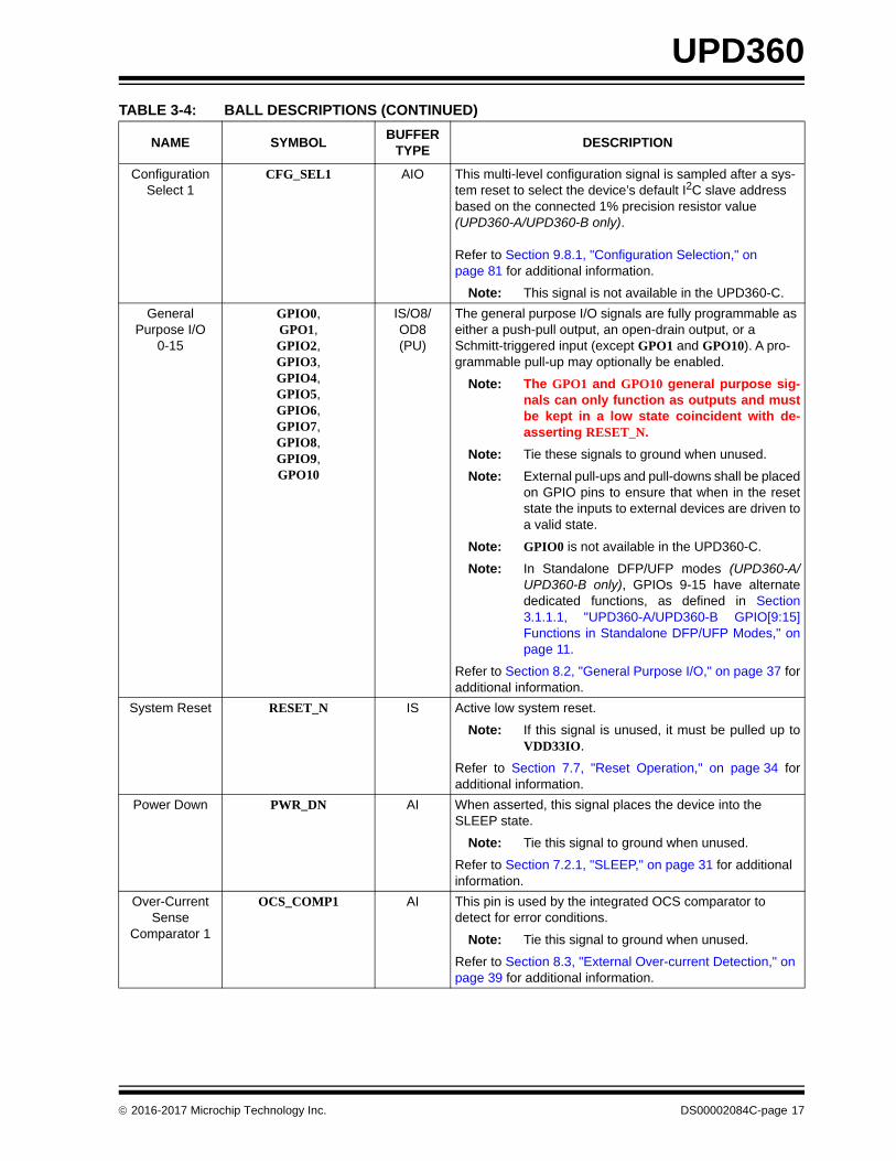
Configuration Select 1
CFG_SEL1 AIO This multi-level configuration signal is sampled after a sys-tem reset to select the device’s default I2C slave address based on the connected 1% precision resistor value (UPD360-A/UPD360-B only).
Refer to Section 9.8.1, "Configuration Selection," on page 81 for additional information.
Note: This signal is not available in the UPD360-C.
General Purpose I/O
0-15
GPIO0,GPO1,GPIO2,GPIO3,GPIO4,GPIO5,GPIO6,GPIO7,GPIO8,GPIO9,GPO10
IS/O8/OD8(PU)
The general purpose I/O signals are fully programmable as either a push-pull output, an open-drain output, or a Schmitt-triggered input (except GPO1 and GPO10). A pro-grammable pull-up may optionally be enabled.
Note: The GPO1 and GPO10 general purpose sig-nals can only function as outputs and mustbe kept in a low state coincident with de-asserting RESET_N.
Note: Tie these signals to ground when unused.
Note: External pull-ups and pull-downs shall be placedon GPIO pins to ensure that when in the resetstate the inputs to external devices are driven toa valid state.
Note: GPIO0 is not available in the UPD360-C.
Note: In Standalone DFP/UFP modes (UPD360-A/UPD360-B only), GPIOs 9-15 have alternatededicated functions, as defined in Section3.1.1.1, "UPD360-A/UPD360-B GPIO[9:15]Functions in Standalone DFP/UFP Modes," onpage 11.
Refer to Section 8.2, "General Purpose I/O," on page 37 foradditional information.
System Reset RESET_N IS Active low system reset.
Note: If this signal is unused, it must be pulled up toVDD33IO.
Refer to Section 7.7, "Reset Operation," on page 34 foradditional information.
Power Down PWR_DN AI When asserted, this signal places the device into the SLEEP state.
Note: Tie this signal to ground when unused.
Refer to Section 7.2.1, "SLEEP," on page 31 for additional information.
Over-Current Sense
Comparator 1
OCS_COMP1 AI This pin is used by the integrated OCS comparator to detect for error conditions.
Note: Tie this signal to ground when unused.
Refer to Section 8.3, "External Over-current Detection," on page 39 for additional information.
TABLE 3-4: BALL DESCRIPTIONS (CONTINUED)
NAME SYMBOLBUFFER
TYPEDESCRIPTION
2016-2017 Microchip Technology Inc. DS00002084C-page 17

UPD360
Over-Current Sense
Comparator 2
OCS_COMP2 AI This pin is used by the integrated OCS comparator to detect for error conditions.
Note: Tie this signal to ground when unused.
Refer to Section 8.3, "External Over-current Detection," on page 39 for additional information.
No Connect NC - For proper operation, this pin must be left unconnected.
Power/Ground
+3.3VVoltage SwitchSupply
VSW P +3.3V power supply output from the integrated power switch.
Note: This pin also provides capacitance for integratedpower switch and must be connected to a 1 uF(<100 Mohm ESR) capacitor to ground.
+3.3VVBUS Supply
3V3_VBUS P +3.3V power supply input derived from VBUS to the inte-grated power switch.
Note: This pin must be connect to a 2.2 uF capacitorto ground.
+3.3VAlways Supply
3V3_ALW P +3.3V main power supply input to the integrated power switch.
Note: This pin must be connect to a 2.2 uF capacitorto ground.
+3.3V I/O Power Supply
Input
VDD33IO P +3.3V I/O power supply input.
+1.8V Digital Core Power
Supply Capaci-tor
VDD18_CAP P +1.8V digital core power supply capacitor. This signal must be connected to a 1uF capacitor to ground for proper oper-ation.
VBUSPort Power
Switch Output
VBUS P Port power switch output.
Note: Both VBUS signals must be tied together.
+5V Port Power Switch Input
VS
P
+5V input to port power switch.
Note: Both VS signals must be tied together.
Note: A 1uF capacitor to ground is required on this sig-nal for a single port configuration. If more thanone port is used, an additional 1uF of capaci-tance must be added for each additional port.
Ground VSS P Ground pins.
TABLE 3-4: BALL DESCRIPTIONS (CONTINUED)
NAME SYMBOLBUFFER
TYPEDESCRIPTION
DS00002084C-page 18 2016-2017 Microchip Technology Inc.

2016-2017 Microchip Technology Inc. DS00002084C-page 19
UPD360
4.0 REGISTER MAP
This chapter provides the device register map, summarizing the various directly addressable System Control and StatusRegisters (CSRs). All CSRs are directly accessible via the device’s internal I2C Slave Controller (UPD360-A/UPD360-B Only) or SPI Slave Controller (UPD360-C Only). Detailed descriptions of the System CSRs are provided in the chap-ters corresponding to their function. Table 4-1 provides a summary of all directly addressable CSRs and their corre-sponding addresses.
Note: Register bit type definitions are provided in Section 1.3, "Register Nomenclature," on page 6.
TABLE 4-1: DEVICE REGISTER MAP
Address Registers
3400h-FFFFh RESERVED
3000h-33FFh Watchdog Timer Registers
2C00h-2FFFh RESERVED
2800h-2BFFh Baseband CC Interface Registers
2000h-27FFh RESERVED
1C00h-1FFFh Power Switch Registers
1800h-1BFFh Power Delivery MAC Registers
1400h-17FFh RESERVED
1000h-13FFh Clocks and Power Management Registers
0C00h-0FFFh DisplayPort HPD Registers
0800h-0BFFh Cable Orientation and Detection Registers
0400h-07FFh Port Power Controller Registers
0000h-03FFh System Control Registers
Note: RESERVED address space must not be written under any circumstances. Failure to heed this warn-ing may result in untoward operation and unexpected results.

UPD360
5.0 I2C SLAVE CONTROLLER (UPD360-A/UPD360-B ONLY)
This chapter details the integrated I2C slave controller (I2C_DAT and I2C_CLK) available in the UPD360-A (+1.8V sig-naling) and UPD360-B (+3.3V signaling). The I2C slave controller can be used for Host CPU serial management anddata transfer, and allows host access to all device Configuration and Status Registers (Section 4.0, "Register Map," onpage 19).
5.1 I2C Overview
I2C is a bi-directional 2-wire data protocol. A device that is currently sending data is defined as the “transmitter” and adevice that is currently receiving data is defined as the “receiver”. The bus is controlled by a master which generatesthe SCL clock, controls bus access, and generates the start and stop conditions. The master and slave will operate astransmitter or receiver, bit-by-bit, as determined by the master. Since the device I2C controller is a slave only, the terms“host” and “master” are synonymous, both referring to the external side of the interface.
Both the clock (SCL) and data (SDA) signals have analog input filters that reject pulses that are less than 50 ns. Thedata pin is driven low when either interface sends a low, emulating the wired-AND function of the I2C bus. Since theslave interface never drives the clock pin, the wired-AND is not necessary.
The following bus states exist:
• Idle: Both I2C_DAT and I2C_CLK are high when the bus is idle.
• Start & Stop Conditions: A start condition (S) is defined as a high to low transition on the SDA line while SCL is high. A stop condition (P) is defined as a low to high transition on the SDA line while SCL is high. The bus is con-sidered to be busy following a start condition and is considered free 4.7 µs / 1.3 µs / 0.5µs (for 100 kHz / 400 kHz / 1MHz operation, respectively) following a stop condition. The bus stays busy following a repeated start condition (Sr) in the absence of a stop condition. Stop/start sequences and repeated starts are otherwise functionally equiv-alent.
• Data Valid: Data is valid, following the start condition, when SDA is stable while SCL is high. Data can only be changed while the clock is low. There is one valid bit per clock pulse. Every byte must be 8 bits long and is trans-mitted MSB first.
• Acknowledge: Each byte of data is followed by an acknowledge bit. The master generates a ninth clock pulse for this bit, and the transmitter releases SDA (high). To provide a positive “acknowledge” (ACK), the receiver drives SDA low so that it remains valid during the high period of the clock, taking into account the setup and hold times. To provide a negative “no-acknowledge” (NACK or ACK), the receiver will allow the line to remain high during this bit time. The receiver may be the master or the slave depending on the direction of the data. Typically the receiver acknowledges each byte. If the master is the receiver, it does not generate an acknowledge on the last byte of a transfer. This informs the slave to not drive the next byte of data, freeing SDA so that the master may generate a stop or repeated start condition.
Figure 5-1 displays the various bus states of a typical I2C cycle.
FIGURE 5-1: I2C CYCLES
I2C_DAT
I2C_CLK
S
Start Condition
P
Stop ConditionData Valid or Ack
Data Valid or Ack
datastable
data can
changedata
stable
data can
change
Sr
Re-Start Condition
data can
change
data can
change
DS00002084C-page 20 2016-2017 Microchip Technology Inc.

UPD360
5.2 I2C Slave Operation
The I2C slave serial interface consists of a data wire (I2C_DAT) and a serial clock (I2C_CLK). The serial clock is drivenby the master, while the data wire is bi-directional. Both signals are open-drain and require external pull-up resistors.
The I2C slave controller implements the low level I2C slave serial interface (start and stop condition detection, data bittransmission/reception and acknowledge generation/reception), handles the slave command protocol and performssystem register reads and writes. It tolerates and also provides clock stretching, in particular for supporting a transparentWake on Host Access (see Section 7.3, "Asynchronous I2C Wakeup (UPD360-A/UPD360-B Only)," on page 32).
The I2C slave controller conforms to the NXP I2C-Bus Specification (UM10204, April 4, 2014), and supports traffic asdefined therein for the following modes:
• Standard-mode (Sm, 100 kbit/s)
• Fast-mode (Fm, 400 kbit/s)
• Fast-mode Plus (Fm+, 1 Mbit/s)
Refer to Section 16.6.2, "I2C Slave Interface (UPD360-A/UPD360-B only)," on page 210 for timing information.
5.2.1 I2C SLAVE COMMAND FORMAT
The I2C slave serial interface supports single register and multiple register Read and Write commands. A Read or Writecommand is started by the master first sending a Start condition, followed by a Control byte. The Control byte consistsof a 7-bit slave address and a 1-bit Read/Write indication (R/~W). The default slave address used by the device isselected via the CFG_SEL1 configuration strap. Assuming the slave address in the Control byte matches this address,the Control byte is acknowledged by the device. Otherwise, the entire sequence is ignored until the next Start condition.The I2C slave controller also supports the General Call Address. The I2C command formats can be seen in Figure 5-2,Figure 5-4, and Figure 5-5.
If the read/write indication (R/~W) in the Control byte is a 0 (Write), the next two bytes sent by the master are a registeraddress, and these two bytes are mandatory. The upper (first) two bits of the address field are a Direction control (DIR),which indicates whether multi-byte accesses will increment, decrement, or fix (as static) the issued address(Section 5.2.2). After the address bytes are acknowledged by the device, the master may send data bytes, which willbe written to successive registers starting at this address. It may instead send another Start condition (to start the read-ing of data) or a Stop condition (only setting the address). The latter two will terminate the current Write before writingany data, but will have the effect of setting the internal register address which will be used for subsequent Reads.
If the read/write indication (R/~W) in the Control byte is a 1 (Read), the device will start sending data following the Con-trol byte acknowledge bit. Read commands cannot designate an address by themselves, but may optionally be prefixedwith a Write command to set it (see Figure 5-4, prefixes in gray). If however the Read immediately follows a MultipleRegister Write or Read, the address may have been incremented or decremented internally according to its DIR field,so this Read will start its access at the next successive byte address. Also, regardless of the previous access, a multiple-byte Read will continue the Increment/Decrement internally, as determined by the previously-issued DIR field(Section 5.2.2).
The length of the register address field is always two full bytes. Some high-order bits are don’t-care. Don’t-care registeraddress bits should be sent as ‘0’ always, for upward compatibility.
FIGURE 5-2: I2C SLAVE ADDRESSING
SSA2
SA1
SA0
0
R/~W
Control Byte
A A A A A9
A8
ACK
ACK
Address Byte 1SA6
SA5
SA4
SA3
*
Start orStop orData [7]
DIRA5
A4
A3
A2
A1
A0
ACK
Address Byte 0
A7
A613 12 11 10
Inc / Dec / Static
1415
2016-2017 Microchip Technology Inc. DS00002084C-page 21
UPD360
5.2.2 MULTIPLE-BYTE REGISTER ADDRESS SEQUENCING
The DIR subfield in Address field bits [15:14] determines how multiple-byte sequences will be interpreted. This field isheld internally whenever issued with an address, but is not applied in I2C except in multiple-byte transfers, Read orWrite. The DIR field definitions are as follows:
• DIR = 00b: Selects auto-incrementing of the internally-held register address for subsequent byte accesses in a multiple-byte packet.
• DIR = 10b: Selects auto-decrementing of the internally-held register address for subsequent byte accesses in a multiple-byte packet.
• DIR = 11b: Select a fixed address. No modification of the internal register address will occur, meaning that all sub-sequent accesses, single- or multiple-byte, are made to the same register.
• DIR = 01b: Reserved for future use.
Note that the DIR field is altered only by issuing an address. It remains, affecting any subsequent multiple-byte Readpackets, until altered.
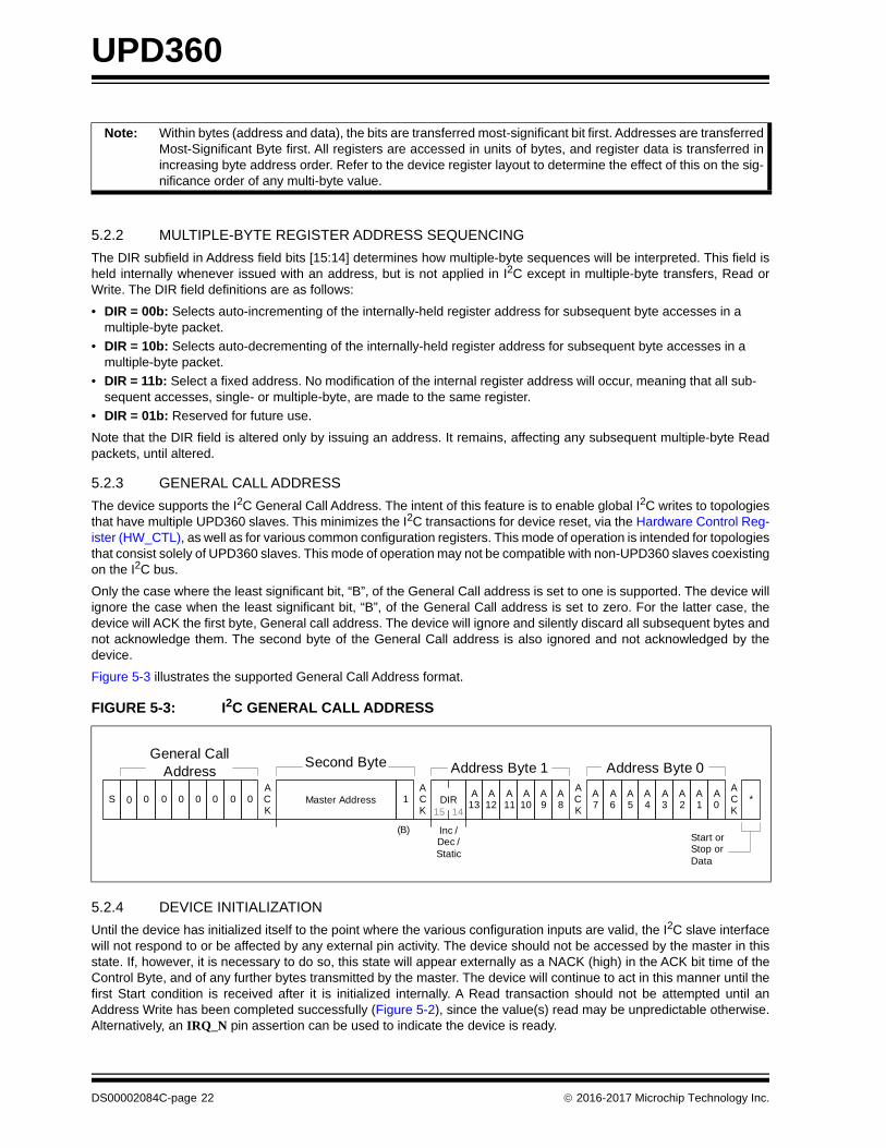
5.2.3 GENERAL CALL ADDRESS
The device supports the I2C General Call Address. The intent of this feature is to enable global I2C writes to topologiesthat have multiple UPD360 slaves. This minimizes the I2C transactions for device reset, via the Hardware Control Reg-ister (HW_CTL), as well as for various common configuration registers. This mode of operation is intended for topologiesthat consist solely of UPD360 slaves. This mode of operation may not be compatible with non-UPD360 slaves coexistingon the I2C bus.
Only the case where the least significant bit, “B”, of the General Call address is set to one is supported. The device willignore the case when the least significant bit, “B”, of the General Call address is set to zero. For the latter case, thedevice will ACK the first byte, General call address. The device will ignore and silently discard all subsequent bytes andnot acknowledge them. The second byte of the General Call address is also ignored and not acknowledged by thedevice.
Figure 5-3 illustrates the supported General Call Address format.
5.2.4 DEVICE INITIALIZATION
Until the device has initialized itself to the point where the various configuration inputs are valid, the I2C slave interfacewill not respond to or be affected by any external pin activity. The device should not be accessed by the master in thisstate. If, however, it is necessary to do so, this state will appear externally as a NACK (high) in the ACK bit time of theControl Byte, and of any further bytes transmitted by the master. The device will continue to act in this manner until thefirst Start condition is received after it is initialized internally. A Read transaction should not be attempted until anAddress Write has been completed successfully (Figure 5-2), since the value(s) read may be unpredictable otherwise.Alternatively, an IRQ_N pin assertion can be used to indicate the device is ready.
Note: Within bytes (address and data), the bits are transferred most-significant bit first. Addresses are transferredMost-Significant Byte first. All registers are accessed in units of bytes, and register data is transferred inincreasing byte address order. Refer to the device register layout to determine the effect of this on the sig-nificance order of any multi-byte value.
FIGURE 5-3: I2C GENERAL CALL ADDRESS
A A A A A9
A8
ACK
ACK
Address Byte 1
*
Start orStop orData
DIRA5
A4
A3
A2
A1
A0
ACK
Address Byte 0
A7
A613 12 11 10
Inc / Dec / Static
14151Master AddressS 0 0 0 0
General Call Address
ACK
0 0 0 0
(B)
Second Byte
DS00002084C-page 22 2016-2017 Microchip Technology Inc.

UPD360
5.2.5 ACCESS DURING AND FOLLOWING POWER MANAGEMENT
During low-power modes, a Start condition will trigger the device to wake, and the device will also stretch the I2C clocklow until its internal clocks are running and locked. It will then release the I2C clock, and process the incoming packet.
It performs these steps before receiving the Slave Address bits, meaning that if there are multiple devices of this typeasleep on the same I2C bus segment then they will all stretch the clock, and they will all wake, regardless of whetherthey were actually addressed. In the event that the slave address of the I2C transaction does not match the value spec-ified in the I2C Slave Address Register (I2C_ADDR) (UPD360-A/UPD360-B Only), the device will power-down automat-ically.
5.2.6 I2C SLAVE READ SEQUENCE
Following the device addressing, as detailed in Section 5.2.1, a register is read from the device when the master sendsa Start condition and Control byte with the R/~W bit set to ‘1’. Assuming the slave address in the Control byte matchesthe device address, the Control byte is acknowledged by the device. Otherwise, the entire sequence is ignored until thenext Start condition. Following the acknowledge, the device sends 1 or more bytes of data, from successive registeraddresses according to the last-issued DIR address subfield (Section 5.2.2), until the master sends a no-acknowledgefollowed by the Stop condition. The no-acknowledge informs the device not to send any further bytes.
The internal register address is unchanged if only a single register byte is read, otherwise (a Multiple Register Read)the internal register address may be incremented or decremented (Section 5.2.2) after each byte including the final one.If the internal address reaches its maximum, it rolls over to 0.
If the master sends an unexpected start or stop condition, the device will stop sending immediately and will respond tothe next sequence as needed.
Figure 5-4 illustrates a typical single and multiple register read. An optional Write of an address is allowed to occur first,shown in gray. Note that this example shows an abbreviated case, where the Write does not have a Stop conditionbefore the Read transfer’s Starts. in this case, the Stop is still allowed, but not required.
5.2.7 I2C SLAVE WRITE SEQUENCE
Following the device addressing, as detailed in Section 5.2.1, a register value is written to the device when the mastercontinues to send data bytes. Each byte is acknowledged by the device. Following any data byte, after the acknowledge,the master may either send another start condition or halt the sequence with a stop condition. The internal registeraddress is unchanged following a single-byte write.
Multiple writes are performed when the master sends additional data bytes following the first. The internal address isautomatically incremented and the next register is written. Once the internal address reaches its maximum value, it rollsover to 0. The multiple write is concluded when the master sends another start or stop condition. In performing a multiplewrite, the internal register address may be incremented or decremented (Section 5.2.2) for each write including the final.
FIGURE 5-4: I2C SLAVE READS
Multiple Register Reads
S
Control Byte
Single Register Read
1D5
D4
D3
D2
D1
D0
ACK
PSA2
SA1
SA0
SA6
SA5
SA4
SA3
ACK
R/~W
Data Byte
D7
D6
SSA2
SA1
SA0
0
Control Byte
A A A A A9
A8
ACK
ACK
Address Byte 1SA6
SA5
SA4
SA3
A5
A4
A3
A2
A1
A0
ACK
Address Byte 0
A7
A613 12 11 10
Data Byte 1
S
Control Byte
1SA2
SA1
SA0
SA6
SA5
SA4
SA3
ACK
D7
D6
SSA2
SA1
SA0
0
Control Byte
A A A A A9
A8
ACK
ACK
Address Byte 1SA6
SA5
SA4
SA3
A5
A4
A3
A2
A1
A0
ACK
Address Byte 0
A7
A613 12 11 10
R/~W
... D1
D0
ACK
Data Bytes 2 — (n-1)
... ACK
Data Byte n
D7
D6
... D1
D0
ACK
P
DIR
Inc / Dec / Static
1415
DIR
Inc / Dec / Static
1415
2016-2017 Microchip Technology Inc. DS00002084C-page 23

UPD360
This is not relevant for subsequent writes after a new Start condition, since a new register address (with its DIR subfield)must then be included. However, this would affect the address used by any subsequent read without first resetting theregister address.
For both single and multiple writes, if the master sends an unexpected start or stop condition, the device will stop imme-diately and will respond to the next sequence as needed.
The data write to a multi-byte register may be delayed until after all bits are input. In the event that the full register is notwritten (master sends a start or a stop condition occurs unexpectedly), the write may be considered invalid and the reg-ister not affected. Multiple registers may be written in a multiple write cycle, each one being written in sequence. I2Cwrites must not be performed to unused register addresses.
Figure 5-5 illustrates a typical single and multiple register write.
5.2.8 SPECIAL CSR HANDLING
5.2.8.1 Live Bits
Register values are latched (registered) at the beginning of each register read to prevent the host from reading a chang-ing value. The latching occurs individually per register in a multiple register read sequence.
5.2.8.2 Change-on-Read Registers and FIFOs
Any single-byte register that triggers a side-effect from a read operation (for example, containing “clear on read” bits, oradvancing a FIFO structure) triggers only after the host has begun accessing the value. The value seen by the masterwill always be the original value and never the updated result of the side-effect.
For a multiple-byte register that is considered a single unit, the change may be delayed until all bytes of the registerhave been read. In the event that the host sends a no-acknowledge on one of the first bytes of a multi-byte register, ora start or stop condition occurs unexpectedly before the acknowledge of the full register, the read may be consideredinvalid and the side-effect not triggered.
Registers read in multiple-register read access will trigger multiple side-effects, occurring as they are read. The followingregisters have read side-effects:
• Watchdog Count Register (WDT_COUNT)
FIGURE 5-5: I2C SLAVE WRITES
Multiple Register Writes
Single Register Write
SSA2
SA1
SA0
0
R/~W
Control Byte
A A A A A9
A8
ACK
ACK
Address Byte 1SA6
SA5
SA4
SA3
A5
A4
A3
A2
A1
A0
ACK
Address Byte 0
A7
A613 12 11 10
D5
D4
D3
D2
D1
D0
P
Data Byte
D7
D6
ACK
Data Byte 1
D7
D6
... D1
D0
ACK
Data Bytes 2 — (n-1)
... ACK
Data Byte n
D7
D6
... D1
D0S
SA2
SA1
SA0
0
R/~W
Control Byte
A A A A A9
A8
ACK
ACK
Address Byte 1SA6
SA5
SA4
SA3
A5
A4
A3
A2
A1
A0
ACK
Address Byte 0
A7
A613 12 11 10
PACK
DIR
Inc / Dec / Static
1415
DIR
Inc / Dec / Static
1415
DS00002084C-page 24 2016-2017 Microchip Technology Inc.

UPD360
5.2.8.3 Live Bits that are also Change-on-Read
As described above, the current value from a register with live bits (as is the case of any register) is captured and latchedas output data, and Change on Read bits are then changed in the original register. To prevent loss of a hardware eventthat occurs following the data capture but before the Change on Read, these hardware events are held pending untilafter the read action and after any change due to the read. This sequence also ensures an edge in the bit due to thehardware event.
2016-2017 Microchip Technology Inc. DS00002084C-page 25
UPD360
6.0 SPI SLAVE CONTROLLER (UPD360-C ONLY)
This chapter details the integrated SPI slave controller (SPI_DI, SPI_DO, SPI_CLK, and SPI_CS) available in theUPD360-C. The SPI slave controller can be used for Host CPU serial management and data transfer, and allows hostaccess to all device Configuration and Status Registers (Section 4.0, "Register Map," on page 19).
6.1 SPI Overview
The SPI Slave module provides a low pin count synchronous slave interface that facilitates communication between thedevice and a host system. The SPI slave allows access to the System CSRs and internal FIFOs and memories. It sup-ports single and multiple register read and write commands with incrementing, decrementing and static addressing.Only a Single bit lane is supported in SPI mode at up to 25 MHz.
The following is an overview of the functions provided by the SPI Slave:
• Fast Read: 4-wire (clock, select, data in and data out) reads. Serial command, address and data. This is called “Fast” Read for historical reasons, and is the only Read command supported. There is a single Dummy byte required for first access. Single and multiple register reads with incrementing, decrementing or static addressing.
• Write: 4-wire (clock, select, data in and data out) writes at up to 25 MHz. Serial command, address and data. Sin-gle and multiple register writes with incrementing, decrementing or static addressing.
6.2 SPI Slave Operation
A SPI frame starts on the falling edge of SPI_CS, and ends with SPI_CS rising. At the edges of SPI_CS, the SPI_CLKclock may be at its reset state of either low (Mode 0) or high (Mode 3), at the option of the Master.
Input data on the SPI_DI pin (often called “MOSI”) is sampled on the rising edge of the SPI_CLK input clock. Outputdata is launched on the SPI_DO pin (often called “MISO”) with the falling edge of the clock. While the SPI_CS chip selectinput is high, the SPI_DI and SPI_CLK inputs are ignored and the SPI_DO output is floating.
Each frame starts with an 8-bit instruction byte, transmitted by the Master, and it is accepted on SPI_DI starting at thefirst rising edge of the input clock after SPI_CS goes active.
For both Write and (Fast) Read instructions, two address bytes follow the instruction byte. The address field expressesa byte address. Fourteen address bits specify the address. The remaining two bits [15:14] constitute the DIR subfieldof the address field, which specifies whether the address is Auto-Incremented (00b) or Auto-Decremented (10b) for con-secutive data bytes in the frame. A special Static address coding (11b) keeps the address static throughout the frameof data, causing a single byte address to be accessed repeatedly if multiple bytes are transferred in the frame. DIR sub-field encoding 01b is reserved and should be decoded in implementation to be the same as 00b, for the sake of mini-mizing the effect of a software error that increments beyond the address space.
For the Fast Read instruction, one dummy byte follows the address bytes. The dummy byte occupies 8 bits, one perclock.
The device will normally not drive SPI_DO during the Instruction, Address or Dummy byte cycles, but see Section 6.2.2,"Access During and Following Power Management," on page 27 for a special case.
For Fast Read instructions, one or more 8-bit data fields follow the dummy byte. For Write instructions, they immediatelyfollow the address bytes.
Individual bytes in instruction, address and data fields are transferred with the most-significant bit (msb) first. The two-byte Address field is transferred with the most-significant byte (MSB) first. Multi-byte data values are transferred in theorder specified by the DIR subfield of the Address field (bits [15:14]), and so their order can be effectively selected byusing Increment mode (starting from the lowest byte address) or Decrement mode (starting from the highest byteaddress).
The SPI interface supports a minimum time of 50ns between successive commands (a minimum SPI_CS inactive timeof 50ns).
DS00002084C-page 26 2016-2017 Microchip Technology Inc.

UPD360
The instructions supported by the SPI slave controller are listed in Table 6-1. Unsupported instructions are reserved andmust not be used.
6.2.1 DEVICE INITIALIZATION
Until the device has been initialized to the point where the various configuration inputs are valid, the SPI interface willnot respond to or be affected by any external pin activity.
Once device initialization completes, the SPI interface will ignore the pins until a rising edge of SPI_CS is detected.
If the device initialization completes during an active cycle (SPI_CS low), the trailing end of the frame must be seen(SPI_CS returning high) before any internal registers are affected or the state of the SPI interface changes.
The first SPI access after device initialization must always be a dummy read to the SPI Test Register (SPI_TEST)(UPD360-C Only).
6.2.1.1 SPI Slave Read Polling for Initialization Complete
With an external weak pull-up resistor present on SPI_DO, a value of FFh will appear to have been read from any inter-nal register while the device is uninitialized. By verifying the SPI Test Register (SPI_TEST) (UPD360-C Only) has atleast one “0” bit in it, it is possible to tell when the device is initialized.
6.2.2 ACCESS DURING AND FOLLOWING POWER MANAGEMENT
The Wake event on SPI traffic is local to the specific device, and does not affect the states of other devices even on thesame SPI bus. Until waking is complete, the SPI interface holds the SPI_DO pin low for the duration of the SPI_CS lowtime.
Until the device is awake, then, any Read access performed by the Master will appear to have returned all “1” bits. Todetermine when the device is awake and the SPI interface functional, the SPI Test Register (SPI_TEST) (UPD360-COnly) should be repeatedly polled by the Master in separate frames (SPI_CS low then high). Once a correct, non-zerovalue is read, the interface can be considered functional. As an alternative to polling, an IRQ_N pin assertion can beused to indicate the device is ready.
Once the power management mode changes back to ACTIVE, the SPI interface will still ignore the SPI_CLK andSPI_DI pins, following SPI_CS low with SPI_DO low, until SPI_CS is seen high. At the next SPI_CS falling edge, SPIcommunication will continue normally.
At any time after performing SPI traffic, the device will not go back to a non-communicating power state until explicitlyallowed to do so by a command from the SPI Master.
TABLE 6-1: SPI INSTRUCTIONS
Instruction DescriptionBus Bit Width
Inst. CodeAddress
BytesDummy Bytes
Data bytes Max Freq.
Read
FASTREAD Read, higher speed format
1 0Bh 2 1 1 to 25 MHz
Write
WRITE Write 1 02h 2 0 1 to 25 MHz
2016-2017 Microchip Technology Inc. DS00002084C-page 27
UPD360
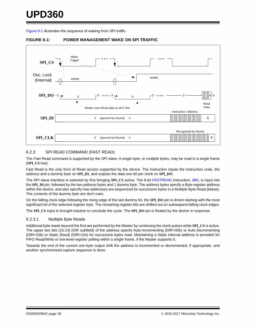
Figure 6-1 illustrates the sequence of waking from SPI traffic.
6.2.3 SPI READ COMMAND (FAST READ)
The Fast Read command is supported by the SPI slave. A single byte, or multiple bytes, may be read in a single frame(SPI_CS low).
Fast Read is the only form of Read access supported by the device. The instruction inputs the instruction code, theaddress and a dummy byte on SPI_DI, and outputs the data one bit per clock on SPI_DO.
The SPI slave interface is selected by first bringing SPI_CS active. The 8-bit FASTREAD instruction, 0Bh, is input intothe SPI_DI pin, followed by the two address bytes and 1 dummy byte. The address bytes specify a Byte register addresswithin the device, and also specify how addresses are sequenced for successive bytes in a Multiple Byte Read (below).The contents of the dummy byte are don’t-care.
On the falling clock edge following the rising edge of the last dummy bit, the SPI_DO pin is driven starting with the mostsignificant bit of the selected register byte. The remaining register bits are shifted out on subsequent falling clock edges.
The SPI_CS input is brought inactive to conclude the cycle. The SPI_DO pin is floated by the device in response.
6.2.3.1 Multiple Byte Reads
Additional byte reads beyond the first are performed by the Master by continuing the clock pulses while SPI_CS is active.The upper two bits [15:14] (DIR subfield) of the address specify Auto-Incrementing (DIR=00b) or Auto-Decrementing(DIR=10b) or Static (fixed) (DIR=11b) for successive bytes read. Maintaining a Static internal address is provided forFIFO Read/Write or low-level register polling within a single frame, if the Master supports it.
Towards the end of the current one-byte output shift the address is incremented or decremented, if appropriate, andanother synchronized capture sequence is done.
FIGURE 6-1: POWER MANAGEMENT WAKE ON SPI TRAFFIC
SPI_CLK
SPI_DI X
SPI_DO ... ZX
SPI_CS
X (Ignored by Device) X
... ...
Osc. Lock(Internal)
Z Z ... Z0 0 Z Z
X (Ignored by Device) X
asleep awake
WakeTrigger
Master sees Read data as all ‘0’ bits.Instruction / Address
Read Data
X
Recognized by Device
DS00002084C-page 28 2016-2017 Microchip Technology Inc.
UPD360
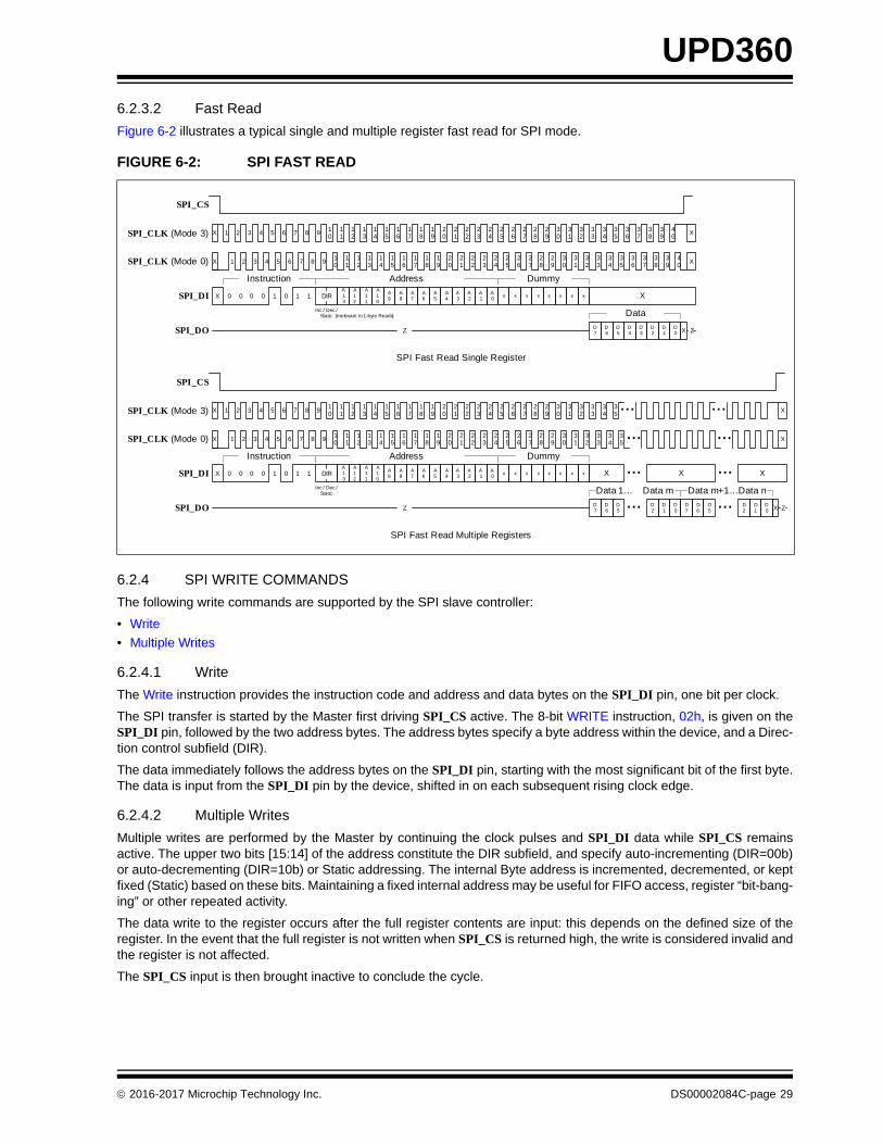
6.2.3.2 Fast Read
Figure 6-2 illustrates a typical single and multiple register fast read for SPI mode.
6.2.4 SPI WRITE COMMANDS
The following write commands are supported by the SPI slave controller:
• Write
• Multiple Writes
6.2.4.1 Write
The Write instruction provides the instruction code and address and data bytes on the SPI_DI pin, one bit per clock.
The SPI transfer is started by the Master first driving SPI_CS active. The 8-bit WRITE instruction, 02h, is given on theSPI_DI pin, followed by the two address bytes. The address bytes specify a byte address within the device, and a Direc-tion control subfield (DIR).
The data immediately follows the address bytes on the SPI_DI pin, starting with the most significant bit of the first byte.The data is input from the SPI_DI pin by the device, shifted in on each subsequent rising clock edge.
6.2.4.2 Multiple Writes
Multiple writes are performed by the Master by continuing the clock pulses and SPI_DI data while SPI_CS remainsactive. The upper two bits [15:14] of the address constitute the DIR subfield, and specify auto-incrementing (DIR=00b)or auto-decrementing (DIR=10b) or Static addressing. The internal Byte address is incremented, decremented, or keptfixed (Static) based on these bits. Maintaining a fixed internal address may be useful for FIFO access, register “bit-bang-ing” or other repeated activity.
The data write to the register occurs after the full register contents are input: this depends on the defined size of theregister. In the event that the full register is not written when SPI_CS is returned high, the write is considered invalid andthe register is not affected.
The SPI_CS input is then brought inactive to conclude the cycle.
FIGURE 6-2: SPI FAST READ
SPI Fast Read Single Register
SPI_CLK (Mode 0)
SPI_DI 0 0 0 0 1X
Instruction
1
Address
SPI_DO
Data
A13
X
SPI Fast Read Multiple Registers
1 0
D7
D6
D5 ZZ X
SPI_CLK (Mode 3)
SPI_CS
X 1 2 3 4 5 6 7 8 9 10
11
12
13
14
15
16
33
34
35
X 1 2 3 4 5 6 7 8 910
11
12
13
14
15
16
33
34
35
37
38
39
40
X
X37
38
39
40
D2
D0
A12
A11
A10
A9
A8
A7
A6
A5
A4
A3
A2
A1
A0
17
18
19
20
21
22
23
24
17
18
19
20
21
22
23
24
SPI_CLK (Mode 0)
SPI_DI X
Instruction Address
X
SPI_DO
A13
...
X...
Z
SPI_CLK (Mode 3)
SPI_CS
...X 1 2 3 4 5 6 7 8 910
11
12
13
14
15
16
X 1 2 3 4 5 6 7 8 9 10
11
12
13
14
15
16
X
X
A12
A11
A10
A9
A8
A7
A6
A5
A4
A3
A2
A1
A0
17
18
19
20
21
22
23
24
17
18
19
20
21
22
23
24
...D7
D6
D5
D2
D0
...D7
D6
D5 ZX
X...
...
x x x x x x x x
25
26
27
28
29
30
31
32
25
26
27
28
29
30
31
32
Dummy
x x x x x x x x
Dummy
25
26
27
28
29
30
31
25
26
27
28
29
30
31
32
32
33
34
35
33
34
35
0 0 0 0 111 0
D1
D1
Data 1... Data m Data m+1...Data n
...
Inc / Dec / Static
DIR
Inc / Dec / Static
DIR
D4
D3
36
36
D2
D0
D1
(Irrelevant to 1-byte Reads)
2016-2017 Microchip Technology Inc. DS00002084C-page 29

UPD360
Figure 6-3 illustrates a typical SPI single and multiple register write.
6.2.5 SPECIAL CSR HANDLING
6.2.5.1 Live Bits
Register values are latched (registered) at the beginning of each register read to prevent the host from reading a chang-ing value. The latching occurs individually per register in a multiple register read sequence.
6.2.5.2 Change-on-Read Registers and FIFOs
Any single-byte register that triggers a side-effect from a read operation (for example, containing “clear on read” bits, oradvancing a FIFO structure) triggers only after the host has begun accessing the value. The value seen by the masterwill always be the original value and never the updated result of the side-effect.
For a multiple-byte register that is considered a single unit, the change may be delayed until all bytes of the registerhave been read. In the event that the host sends a no-acknowledge on one of the first bytes of a multi-byte register, ora start or stop condition occurs unexpectedly before the acknowledge of the full register, the read may be consideredinvalid and the side-effect not triggered.
Registers read in multiple-register read access will trigger multiple side-effects, occurring as they are read. The followingregisters have read side-effects:
• Watchdog Count Register (WDT_COUNT)
6.2.5.3 Live Bits that are also Change-on-Read
As described above, the current value from a register with live bits (as is the case of any register) is captured and latchedas output data, and Change on Read bits are then changed in the original register. To prevent loss of a hardware eventthat occurs following the data capture but before the Change on Read, these hardware events are held pending untilafter the read action and after any change due to the read. This sequence also ensures an edge in the bit due to thehardware event.
FIGURE 6-3: SPI WRITE
SPI Write Single Register
SPI_CLK (Mode 0)
SPI_DI 0 0 0 0X
Instruction
1
Address
SPI_DO
DataA13
SPI Write Multiple Registers
0 0D7
D6
D5
Z
X
SPI_CLK (Mode 3)
SPI_CS
X 1 2 3 4 5 6 7 8 910
11
12
13
14
15
16
25
26
27
X 1 2 3 4 5 6 7 8 910
11
12
13
14
15
16
25
26
27
29
30
31
32
X
X29
30
31
32
D2
D0
A12
A11
A10
A9
A8
A7
A6
A5
A4
A3
A2
A1
A0
17
18
19
20
21
22
23
24
17
18
19
20
21
22
23
24
SPI_CLK (Mode 0)
SPI_DI 0 0 0 0X
Instruction Address
SPI_DO
A13
...
0 0
Z
SPI_CLK (Mode 3)
SPI_CS
...X 1 2 3 4 5 6 7 8 910
11
12
13
14
15
16
25
26
27
X 1 2 3 4 5 6 7 8 910
11
12
13
14
15
16
25
26
27
X
X
A12
A11
A10
A9
A8
A7
A6
A5
A4
A3
A2
A1
A0
17
18
19
20
21
22
23
24
17
18
19
20
21
22
23
24
...D7
D6
D5
D2
D0
...D7
D6
D5 X
...
D1
D1
Data 1... Data m Data m+1... Data n
...
0
1 0
Inc / Dec / Static
DIR
(Irrelevant to 1-byte Writes)
Inc / Dec / Static
DIR
28
28
D4
D3
D2
D0
D1
DS00002084C-page 30 2016-2017 Microchip Technology Inc.
UPD360
7.0 CLOCKS, RESETS, AND POWER MANAGEMENT
This section details the various clocks, resets, and power managements states of the device:
7.1 Clocks
The following internal clocks are generated by the device:
• 48 MHz Relaxation Oscillator
• 20 KHz Keep Alive Oscillator
• Ring Oscillator
These oscillators can be manually enabled/disabled via the Clock Control Register (CLK_CTL).
7.2 Power States
The device supports four power states, as defined in the following sub-sections:
• SLEEP
• STANDBY
• ACTIVE_PPC_OFF
• ACTIVE_PPC_ON
7.2.1 SLEEP
This is the lowest power state of the device. The SLEEP state is entered via assertion of the PWR_DN pin. Virtually allof the device is powered off in this mode with minimal circuity in the 3.3V domain to detect deassertion of PWR_DN.
This mode is intended to minimize power consumption when the device is not being used in battery powered applica-tions. In these applications, a wake up event such as a button press, can cause the host CPU to deassert PWR_DN.
7.2.2 STANDBY
STANDBY is the lowest power functional state of the device. The majority of the device is powered off in this state. Theinternal CC comparator and 20 KHz oscillator are enabled in this state as well as requisite analog components (1.8VLDO, PORs, Biases, etc).
The CC lines are constantly monitored for an attach condition which shall result in an interrupt assertion to the host. Ifan attachment has been made, this state can detect a change in the partner’s advertisement as well as a detach.
STANDBY is the power state that the UPD360 device will be in when in USB Type-CTM Unattached.SRC/SNK.
The following asynchronous wake-ups are supported from this state:
• Asynchronous I2C Wakeup (UPD360-A/UPD360-B Only)
• Asynchronous SPI Wakeup (UPD360-C Only)
• Power Delivery MAC Wakeup
7.2.3 ACTIVE_PPC_OFF
This state defines the condition where the internal 48 MHz oscillator is enabled, but the Port Power Controller is dis-abled. A use case for this state would be when it is desired to debounce a GPIO for a micro-second period. In that case,the internal 48 MHz oscillator is required to time the debounce.
The device also momentarily enters this state when being addressed via software I2C/SPI accesses or to implementPower Delivery communications.
The UPD360 will be in ACTIVE_PPC_OFF primarily when in USB Type-CTM Attached.SNK state, or Attached.SRCstate with VBUS being driven by an external power source.
7.2.4 ACTIVE_PPC_ON
This state defines the condition where the Port Power Controller is operational, which necessitates the internal 48 MHzoscillator be enabled for the Port Power Controller.
2016-2017 Microchip Technology Inc. DS00002084C-page 31

UPD360
The UPD360 will be in ACTIVE_PPC_ON state when in USB Type-CTM Attached.SRC state with VBUS being drivenby the internal 5V port power controller.
7.3 Asynchronous I2C Wakeup (UPD360-A/UPD360-B Only)
The device supports asynchronous wakes on the I2C slave interface. Via clock stretching, the I2C transaction thatcaused the wakeup will not be lost and does not have to be repeated by the host. The device will not clock stretch formore than 3 us.
The following steps illustrate the I2C wake function. Initially the Ring Oscillator and 48 MHz Oscillator are disabled.
1. The Host initiates an I2C transaction to the device.
2. The device asynchronously detects reception of the Start Bit and enables clock stretching by pulling-down I2C_-CLK after the host drives SCL low. The Ring Oscillator is asynchronously enabled and used as a clock sourcefor the power management logic.
3. After a delay of approximately 5 us the oscillator stabilizes and clocks the I2C controller.
4. Clock stretching is disabled and the I2C controller is enabled and begins processing the pending transaction.
5. The I2C transaction completes.
6. The Host checks the device status to see if there are any pending transactions. The I2C transaction may haveinitiated a PD transmission or conversely a coincident PD transaction may be in the process of being received.
7. After host confirms the device has no pending transactions, it power downs the device by disabling the RingOscillator and 48 MHz Relaxation Oscillator via Clock Control Register (CLK_CTL).
8. The device is ready to accept future asynchronous I2C wake event.
7.4 Asynchronous SPI Wakeup (UPD360-C Only)
UPD360 supports asynchronous wakes on the SPI interface. The SPI protocol for this device is defined such that thereis no requirement that the SPI transaction must be repeated.
The following steps illustrate the SPI wake function. Initially the Ring Oscillator and 48 MHz Oscillator are disabled.
1. The device is powered down.
2. The Host initiates an SPI transaction to the SPI Test Register (SPI_TEST) (UPD360-C Only) which, when thedevice is operational, returns a non-zero value. The device drives SPI_DO to 0b while in power-down.
3. The device detects reception of an SPI message. The Ring Oscillator is asynchronously enabled and used as aclock source for the power management logic.
4. After a delay of approximately 5 us the oscillator stabilizes and clocks the SPI controller.
5. The device processes the next received SPI transaction.
6. The SPI transaction(s) complete(s).
7. The Host checks the device status to see if there are any pending transactions. The SPI transaction may haveinitiated a PD transmission or conversely a coincident PD transaction may be in the process of being received.
8. After the Host confirms the device has no pending transactions, it powers down the device by disabling the RingOscillator, and 48 MHz Relaxation Oscillator via Clock Control Register (CLK_CTL).
9. The device drives SPI_DO to 0b and awaits an asynchronous SPI wake.
DS00002084C-page 32 2016-2017 Microchip Technology Inc.
UPD360
7.5 Power Delivery MAC Wakeup
The PD MAC is capable of asynchronous wakeup upon reception of a PD packet. This enables the device to be placedin STANDBY mode and minimize power consumption.
The following steps illustrate the RX PD MAC wake function. Initially the Ring Oscillator and the 48 MHz RelaxationOscillator are disabled. The 20 KHz Keep Alive Oscillator is enabled, but not used in the wake process.
1. In order to receive a PD message, the RX AFE is enabled via software and the trip point is set via the CC RXDAC Control Register (CC_RX_DAC_CTL) and CC RX DAC Filter Register (CC_RX_DAC_FILT).
2. The PD MAC is configured and enabled via software.
3. The device is powered down. Software disables the 48 MHz Relaxation Oscillator, and Ring Oscillator if enabled,via the Clock Control Register (CLK_CTL).
4. After some time elapses, the device receives a PD message from the attached partner.
5. The PD MAC asynchronously detects preamble activity on the CC line and enables the 48 MHz Relaxation Oscil-lator.
6. The oscillator is operational in approximately 5 us, at which point the PD MAC is operational.
7. The PD MAC receives the remainder of the preamble and stores the message into the RX FIFO, and in accor-dance with the PD protocol, responds with GoodCRC as required.
8. An interrupt is issued via assertion of the IRQ_N pin.
9. Software services the interrupt via I2C, reads the PD message, and responds as required.
10. The device is then powered down. Software disables the 48 MHz Relaxation Oscillator and Ring Oscillator viathe Clock Control Register (CLK_CTL).
11. The device remains powered down until the next PD message is received.
7.6 Interrupt Assertion from STANDBY
When the device is in STANDBY it is able to detect a number of events that may be configured to assert the IRQ_N pinupon being appropriately programmed via software. The logic detecting such events operates off of the 20 KHz KeepAlive Oscillator.
Upon the occurrence of an event, which is programmed to assert IRQ_N, the 48 MHz Relaxation Oscillator and RingOscillator are enabled. Upon synchronization, the IRQ_N pin shall assert.
After software services the source interrupt(s), it should disable the 48 MHz Relaxation Oscillator and Ring Oscillatorvia the Clock Control Register (CLK_CTL) to place the part back in STANDBY.
The following example sequence illustrates the steps for configuring the device to detect an OCS event on the OCS_-COMP1 pin while in STANDBY.
1. Software enables the OCS_CMP_INT bit in the Interrupt Enable Register (INT_EN).
2. Software enables OCS detection, as defined in Section 8.3, "External Over-current Detection", to sample theOCS_COMP1 pin.
3. Software disables the 48 MHz Relaxation Oscillator and Ring Oscillator via the Clock Control Register(CLK_CTL).
4. An OCS event occurs and is detected on OCS_COMP1.
5. The Ring Oscillator is enabled and is used to as the device’s operational clock.
6. The device enables the 48 MHz oscillator and waits about 5 us for the oscillator to stabilize.
7. The 48 MHz oscillator is stable.
8. After synchronization is complete, the IRQ_N pin is asserted.
9. Software detects IRQ_N assertion and services the interrupt.
10. Software disables the 48 MHz Relaxation Oscillator and Ring Oscillator via the Clock Control Register(CLK_CTL) to place the part back in STANDBY.
2016-2017 Microchip Technology Inc. DS00002084C-page 33

UPD360
7.7 Reset Operation
The following chip-level resets are supported by the device:
• Power-On-Reset (POR)
• Pin Reset (RESET_N)
• Software Reset (SRESET in Hardware Control Register (HW_CTL))
• Watchdog Timer (WDT_STS)
Chip-level resets trigger the sampling of the CFG_SEL0 and CFG_SEL1 configuration straps (see Section 9.8.1, "Con-figuration Selection," on page 81 for additional information). Chip-level reset completion can be determined by assertionof the RDY_INT bit in the Interrupt Enable Register (INT_EN) and assertion of the IRQ_N pin.
The following is s summary of steps that occur after a chip-level reset.
1. System level reset event (POR, RESET_N, SRESET, WDT_STS) occurs.
2. The device enables the 20 KHz Keep Alive Oscillator, 48 MHz Relaxation Oscillator, and 1MHz Ring Oscillator.
3. The device samples the CFG_SELx pins.
4. The device configures itself in accordance with the CFG_SELx pin and settings.
5. The device is enabled, the RDY_INT bit in the Interrupt Enable Register (INT_EN) asserts, the IRQ_N pinasserts.
6. The device disables the 48 MHz Relaxation Oscillator and the Ring Oscillator.
7.8 Clocks and Power Management Registers
This section details the clocks and power management registers. For an overview of the entire device register map, referto Section 4.0, "Register Map," on page 19.
7.8.1 CLOCK CONTROL REGISTER (CLK_CTL)
Note 7-1 This bit will always appear asserted when read by software, as the 48 MHz Relaxation Oscillator mustbe enabled to facilitate I2C/SPI transactions.
TABLE 7-1: CLOCKS AND POWER MANAGEMENT REGISTERS MAP
Address Register Name (Symbol)
1000h Clock Control Register (CLK_CTL)
1001h – 13FFh Reserved for future expansion
Note: RESERVED address space must not be written under any circumstances. Failure to heed this warn-ing may result in untoward operation and unexpected results.
Address: 1000h Size: 8 bits
Bits Description Type Default
7:3 RESERVED RO -
2 Ring Oscillator Enable0: Oscillator is disabled.1: Oscillator is enabled.
R/W 0b
1 48 MHz Relaxation Oscillator Enable0: Oscillator is disabled.1: Oscillator is enabled.
R/W Note 7-1
0 20 KHz Keep Alive Oscillator Enable0: Oscillator is disabled.1: Oscillator is enabled.
R/W 1b
DS00002084C-page 34 2016-2017 Microchip Technology Inc.
UPD360
8.0 SYSTEM CONTROL
This section details the following system controls:
• System Interrupts
• General Purpose I/O
• External Over-current Detection
• System Control Registers
8.1 System Interrupts
The device provides an open drain interrupt pin, IRQ_N, which is asserted as a function of the System Control’s InterruptStatus Register (INT_STS) and Interrupt Enable Register (INT_EN). The following interrupts are supported:
• HPD Interrupt
• Power Switch Module Interrupt
• Watchdog Timer Assertion Interrupt
• Port Power Controller Interrupt
• Power Delivery MAC Interrupt
• OCS Comparator Interrupt
• PIO Override Interrupt
• PIO Interrupt
• CC Interrupt
• VBUS Interrupt
• Power Control Interrupt
• Device Ready Interrupt
In order to clear an interrupt status bit, the source of the asserted bit in Interrupt Status Register (INT_STS) must becleared. This process typically involves dealing with the module (e.g. PD MAC, CC, Port Power Controller, WatchdogTimer, Power Switch, etc.) that triggered the interrupt or configuring the respective module’s interrupt enable register todisable assertion.
The PIO interrupts are cleared by writing “1” to the asserted bit(s) in PIO Interrupt Status Register (PIO_INT_STS). ThePIO Override interrupts are cleared by writing “1” to the asserted bit(s) in PIO Override Interrupt Status Register(PIO_OVR_INT_STS). The OCS interrupts are cleared by is cleared by writing “1” to the asserted bit(s) in OCS Com-parator Change Status Register (OCS_CMP_CHG_STS).
Figure 8-1 illustrates the device’s interrupt hierarchy. Figure 8-2 illustrates the generation of the CC_INT bit in the Inter-rupt Status Register (INT_STS).
2016-2017 Microchip Technology Inc. DS00002084C-page 35

UPD360
FIGURE 8-1: SYSTEM INTERRUPT HIERARCHY
IRQ_N Pin
System Control.INT_STS[0]
System Control.INT_EN[0]
PSW Interrupt
System Control.INT_EN[7]
System Control.INT_STS[1]
System Control.INT_EN[1]
PIO_INT[0]
PIO_EN[0]
PIO_INT[15]
PIO_EN[15]
System Control.INT_STS[2]
System Control.INT_EN[2]
PIO_OVR_INT[0]
PIO_OVR_EN[0]
PIO_OVR_INT[3]
PIO_EN[3]
System Control.INT_STS[3]
System Control.INT_EN[3]
OCS Comparator Match
System Control.INT_STS[7]
System Control.INT_STS[4]
System Control.INT_EN[4]
PD MAC Interrupt
System Control.INT_STS[5]
System Control.INT_EN[5]
PPC Interrupt
System Control.INT_STS[6]
System Control.INT_EN[6]
WDT Event
CC_INT Interrupt
HPD Interrupt
System Control.INT_EN[8]
System Control.INT_STS[8]
VBUS Change Interrupt
System Control.INT_EN[9]
System Control.INT_STS[9]
VBUS_MATCH_EN[7]
VBUS_CHG_STS[7]
VBUS_MATCH_EN[0]
VBUS_CHG_STS[0]
System Control.INT_EN[10]
System Control.INT_EN[11]
Power Event InterruptSystem Control.INT_STS[10]
System Control.INT_STS[11]RESERVED
System Control.INT_EN[12]
Device ReadySystem Control.INT_STS[12]
DS00002084C-page 36 2016-2017 Microchip Technology Inc.
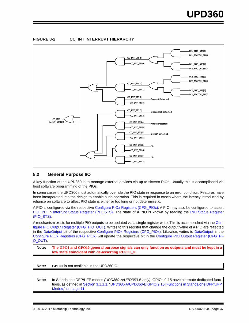
UPD360
8.2 General Purpose I/O
A key function of the UPD360 is to manage external devices via up to sixteen PIOs. Usually this is accomplished viahost software programming of the PIOs.
In some cases the UPD360 must automatically override the PIO state in response to an error condition. Features havebeen incorporated into the design to enable such operation. This is required in cases where the latency introduced byreliance on software to affect PIO state is either or too long or not deterministic.
A PIO is configured via the respective Configure PIOx Registers (CFG_PIOx). A PIO may also be configured to assertPIO_INT in Interrupt Status Register (INT_STS). The state of a PIO is known by reading the PIO Status Register(PIO_STS).
A mechanism exists for multiple PIO outputs to be updated via a single register write. This is accomplished via the Con-figure PIO Output Register (CFG_PIO_OUT). Writes to this register that change the output value of a PIO are reflectedin the DataOutput bit of the respective Configure PIOx Registers (CFG_PIOx). Likewise, writes to DataOutput in theConfigure PIOx Registers (CFG_PIOx) will update the respective bit in the Configure PIO Output Register (CFG_PI-O_OUT).
FIGURE 8-2: CC_INT INTERRUPT HIERARCHY
Note: The GPO1 and GPO10 general purpose signals can only function as outputs and must be kept in alow state coincident with de-asserting RESET_N.
Note: GPIO0 is not available in the UPD360-C.
Note: In Standalone DFP/UFP modes (UPD360-A/UPD360-B only), GPIOs 9-15 have alternate dedicated func-tions, as defined in Section 3.1.1.1, "UPD360-A/UPD360-B GPIO[9:15] Functions in Standalone DFP/UFPModes," on page 11
CC_INT_STS[6]
CC_INT_EN[6]
CC_INT_STS[7]
CC_INT_EN[7]
0b
0b
CC_INT_EN[5]
Detach Detected
CC_INT_EN[4]
Attach Detected
CC_INT_STS[5]
CC_INT_STS[4]
CC_INT_EN[3]
Disconnect DetectedCC_INT_STS[3]
CC_INT_STS[1]
CC_INT_EN[1]
CC_INT_STS[2]
CC_INT_EN[2]
Connect Detected
CC_INT_EN[0]
CC_INT_STS[0]
CC2_MATCH_EN[7]
CC2_CHG_STS[7]
CC2_MATCH_EN[0]
CC2_CHG_STS[0]
CC2_MATCH_EN[7]
CC1_CHG_STS[7]
CC1_MATCH_EN[0]
CC1_CHG_STS[0]
CC_INT(to INT_STS[0])
2016-2017 Microchip Technology Inc. DS00002084C-page 37
UPD360
8.2.1 PIO SIMULTANEOUS UPDATE
A mechanism has been incorporated to enable multiple PIOs to be updated simultaneously. This is desirable to simplifysoftware and prevent devices controlled by the UPD360 from entering an intermediary unknown state. Of particular con-cern would be devices responsible for managing power.
The Configure PIOx Registers (CFG_PIOx) CSR is updated by this function. When the simultaneous update request isaccepted by hardware, the contents of the PIO registers are simultaneously updated.
The example below illustrates simultaneous PIO update operation:
1. Software changes Configure PIOx Update Registers (CFG_PIOx_UPD) as required.
2. Software changes Configure PIO Output Update Register (CFG_PIO_OUT_UPD) as required.
3. Software sets the Configure PIOx Update Registers (CFG_PIOx_UPD) to initiate the update.
4. A pending PIO override blocks acceptance of the update request. Only after the pending PIO override functionis cleared will the device clear PIO_UPD_REQ. The pending PIO override is cleared via the PIO Override EnableRegister (PIO_OVR_EN).
5. After the update is accepted, PIO_UPD_REQ clears automatically.
APPLICATION NOTE: If a PIO override is pending, the PIO simultaneous update is blocked.
8.2.2 PIO OVERRIDE
8.2.2.1 Overview
A mechanism is defined in this section to enable the state of a PIO to be changed without software intervention. Thisprovides a mechanism to instantaneously disable a power circuit, controlled by a UPD360 PIO, based upon a changein the state of a selected PIO input, OCS detection or other event.
8.2.2.2 Description
Four override functions are included in device. For each function, a PIO or other source must be selected for monitoringvia the corresponding PIO Override x Source Select Registers (PIO_OVRx_SRC_SEL). The value to be monitored isset in the PIO Override Monitor Value Register (PIO_OVR_MON_VAL) and is compared with the state of the respectivePIO. When these values match for an override, the enabled PIO outputs change their state accordingly.
PIO outputs controlled by an override are enabled by the PIO Override x Output Enable Registers (PIO_OVRx-_OUT_EN). Each override has an instance in this register. A PIO may be used across multiple overrides.
Firmware can be notified that an override was executed via assertion of PIO_OVERRIDE_INT in the Interrupt StatusRegister (INT_STS), if Interrupt Enable Register (INT_EN) is appropriately configured.
Note: The Configure PIO Output Update Register (CFG_PIO_OUT_UPD) and Configure PIOx Update Registers(CFG_PIOx_UPD) must be programmed consistently by software. If the output value bits are differentbetween the two registers, then the value in Configure PIOx Update Registers (CFG_PIOx_UPD) will beused for updating the Configure PIOx Registers (CFG_PIOx) and the respective bit in Configure PIO Out-put Register (CFG_PIO_OUT).
DS00002084C-page 38 2016-2017 Microchip Technology Inc.

UPD360
8.3 External Over-current Detection
The device incorporates an analog comparator DAC circuit to detect an over-current condition. This feature is supportedvia the OCS_COMP1 and/or OCS_COMP2 pin.
This feature is enabled as follows:
1. Software clears the OCS Comparator Control bit in the OCS Comparator Control Register (OCS_CMP_CTL) todetermine the OCS debouncer.
2. Software polls OCS_DB_ACTIVE until it clears, which indicates the OCS debouncer is disabled.
3. If OCS_COMP2 is desired, the shared PIO must be disabled via the Configure PIOx Registers (CFG_PIOx).
4. Software programs one or both of the OCS Comparator x Threshold Registers (OCS_CMPx_THR), as required.
5. Software programs the OCS Comparator Debounce Register (OCS_CMP_DEBOUNCE).
6. Software enables the OCS_COMPx pin(s) via the OCS Comparator Match Enable Register (OCS_CMP_-MATCH_EN).
7. Software enables the respective interrupt in the Interrupt Enable Register (INT_EN).
8. Software sets the OCS Comparator Control bit in the OCS Comparator Control Register (OCS_CMP_CTL) toenable comparison on OCS_COMP1 and/or OCS_COMP2, as desired.
9. Detection of an over current event by the comparator results in the respective bit of the OCS Comparator ChangeStatus Register (OCS_CMP_CHG_STS) and OCS_CMP_INT asserts. The IRQ_N pin will assert, if configured.
10. Software writes to the OCS Comparator Change Status Register (OCS_CMP_CHG_STS) to clear OCS_C-MP_INT. For a Lo-to-Hi transition, the respective bit in the OCS Comparator Match Register (OCS_CMP_-MATCH) is set, while for a Hi-to-Lo transition the bit is cleared.
This feature is disabled when software clears the OCS Comparator Control bit in the OCS Comparator Control Register(OCS_CMP_CTL). Either OCS_COMPx pin may be used to trigger a PIO override.
8.4 General Purpose Timer
The device incorporates a low power general purpose timer that operates off a 20 kHz oscillator and implements a 16-bit one-shot down counter. When the timer underflows, it asserts the GP_UFLOW bit in General Purpose Timer InterruptSource Register (GP_TIMER_INT_SRC) and stops counting. This in turn causes the GP_TIMER_INT to assert in Inter-rupt Status Register (INT_STS). The interrupt persists until the GP_UFLOW bit is cleared. If the respective bit is set inInterrupt Enable Register (INT_EN), the IRQ_N pin will assert.
The timer’s upper threshold is loaded via the General Purpose Timer Load Register (GP_TIMER_LOAD). SettingRESET in the General Purpose Timer Control Register (GP_TIMER_CTL) causes the timer’s internal counter to beloaded to this value.
The timer is enabled by setting ENABLE in the General Purpose Timer Control Register (GP_TIMER_CTL). This causesthe timer to decrement every 1 ms. The timer continues to decrement until it underflows or it is disabled.
Clearing the ENABLE bit in the General Purpose Timer Control Register (GP_TIMER_CTL) disables the timer and itstops counting.
The timer’s current count can be read from General Purpose Timer Count Register (GP_TIMER_COUNT) The timershould be halted by clearing ENABLE before reading it. After the count is read, the ENABLE may be set again and thecounter will resume.
The DIS_ON_UFLOW bit in the General Purpose Timer Control Register (GP_TIMER_CTL) causes the timer to auto-matically disable upon underflow detection and assert GP_UFLOW. In this case the assertion of GP_UFLOW is delayeduntil the timer is fully disabled.
APPLICATION NOTE: This timer enables clocking sources to be disabled in the host CPU which is useful for timingevents such as DRP. This helps provide for a lower total power system solution.
The following steps illustrate the usage model for DRP implementation:
1. Software configures the device as a DFP or UFP. See Section 9.4, "DRP Operation" for further details.
2. Software enables the GP_TIMER_INT in the Interrupt Enable Register (INT_EN).
Note: The underflow condition is defined as when the down counter transitions from 0x0000 to 0xFFFF.
2016-2017 Microchip Technology Inc. DS00002084C-page 39
UPD360
3. Software programs the General Purpose Timer Load Register (GP_TIMER_LOAD) to a random value that com-plies with the range for tDRP period as defined in the USB Type-C Specification.
4. Software sets the ENABLE, RESET and DIS_ON_UFLOW bits in the General Purpose Timer Control Register(GP_TIMER_CTL). This causes the value in the General Purpose Timer Load Register (GP_TIMER_LOAD) tobe loaded into the timer and it begins decrementing. This also configures the timer to delay assertion of GP_U-FLOW in the General Purpose Timer Interrupt Source Register (GP_TIMER_INT_SRC) until the timer is fully dis-abled .
APPLICATION NOTE: Writes to General Purpose Timer Load Register (GP_TIMER_LOAD) and General PurposeTimer Control Register (GP_TIMER_CTL) defined in the prior steps may be done in thesame I2C write burst.
5. Upon timer expiration, the GP_UFLOW bit will be set and the GP_TIMER_INT asserts in Interrupt Status Register(INT_STS).
6. The IRQ_N pin asserts.
7. Software services the IRQ and determines whether or not a connection has been established with a UFP, or DFP.If no connection has been established, software changes the device’s role. See Section 9.4, "DRP Operation" forfurther details.
8. Software programs the General Purpose Timer Load Register (GP_TIMER_LOAD) to a random value that com-plies with the range of the tDRP period as defined in the USB Type-C Specification.
9. Software shall clear the GP_UFLOW bit in the General Purpose Timer Interrupt Source Register (GP_TIM-ER_INT_SRC).
10. Software sets the ENABLE, RESET and DIS_ON_UFLOW bits in General Purpose Timer Control Register (GP_-TIMER_CTL). This causes the value in General Purpose Timer Load Register (GP_TIMER_LOAD) to be loadedinto the timer and the timer begins decrementing.
APPLICATION NOTE: Writes to the General Purpose Timer Load Register (GP_TIMER_LOAD), General PurposeTimer Interrupt Source Register (GP_TIMER_INT_SRC) and General Purpose Timer ControlRegister (GP_TIMER_CTL) defined in the prior steps may be done in the same I2C writeburst.
11. Upon timer expiration, and timer disablement, the GP_UFLOW bit will be set and the GP_TIMER_INT asserts inInterrupt Status Register (INT_STS).
12. The IRQ_N pin asserts.
13. Software services the IRQ and determines if a connection has been established with a UFP, or DFP. If no con-nection has been established SW changes the device’s role. See Section 9.4, "DRP Operation" for further details.
14. Goto step 8.
DS00002084C-page 40 2016-2017 Microchip Technology Inc.

UPD360
8.5 System Control Registers
This section details the system control registers. For an overview of the entire device register map, refer to Section 4.0,"Register Map," on page 19.
TABLE 8-1: SYSTEM CONTROL REGISTER MAP
Address Register Name (Symbol)
0000h Device ID Register (ID_REV)
0004h USB Vendor ID Register (VID)
0006h USB Product ID Register (PID)
0008h USB PD Revision Register (PD_REV)
000Ah USB Type-C™ Revision Register (C_REV)
000Bh - 000Dh Reserved for future expansion
000Eh SPI Test Register (SPI_TEST) (UPD360-C Only)
0010h Interrupt Status Register (INT_STS)
0014h Interrupt Enable Register (INT_EN)
0018h Hardware Control Register (HW_CTL)
001Ah I2C Slave Address Register (I2C_ADDR) (UPD360-A/UPD360-B Only)
001Bh PPC Status Register (PPC_BUSY)
001Ch - 001Fh Reserved for future expansion
0020h PIO Status Register (PIO_STS)
0022h PIO Interrupt Status Register (PIO_INT_STS)
0024h PIO Interrupt Enable Register (PIO_INT_EN)
0026h - 002Fh Reserved for future expansion
0030h Configure PIOx Registers (CFG_PIOx) x=0
0031h Configure PIOx Registers (CFG_PIOx) x=1
0032h Configure PIOx Registers (CFG_PIOx) x=2
0033h Configure PIOx Registers (CFG_PIOx) x=3
0034h Configure PIOx Registers (CFG_PIOx) x=4
0035h Configure PIOx Registers (CFG_PIOx) x=5
0036h Configure PIOx Registers (CFG_PIOx) x=6
0037h Configure PIOx Registers (CFG_PIOx) x=7
0038h Configure PIOx Registers (CFG_PIOx) x=8
0039h Configure PIOx Registers (CFG_PIOx) x=9
003Ah Configure PIOx Registers (CFG_PIOx) x=10
003Bh Configure PIOx Registers (CFG_PIOx) x=11
003Ch Configure PIOx Registers (CFG_PIOx) x=12
003Dh Configure PIOx Registers (CFG_PIOx) x=13
003Eh Configure PIOx Registers (CFG_PIOx) x=14
003Fh Configure PIOx Registers (CFG_PIOx) x=15
0040h Configure PIOx Update Registers (CFG_PIOx_UPD) x=0
0041h Configure PIOx Update Registers (CFG_PIOx_UPD) x=1
0042h Configure PIOx Update Registers (CFG_PIOx_UPD) x=2
0043h Configure PIOx Update Registers (CFG_PIOx_UPD) x=3
0044h Configure PIOx Update Registers (CFG_PIOx_UPD) x=4
0045h Configure PIOx Update Registers (CFG_PIOx_UPD) x=5
0046h Configure PIOx Update Registers (CFG_PIOx_UPD) x=6
0047h Configure PIOx Update Registers (CFG_PIOx_UPD) x=7
2016-2017 Microchip Technology Inc. DS00002084C-page 41
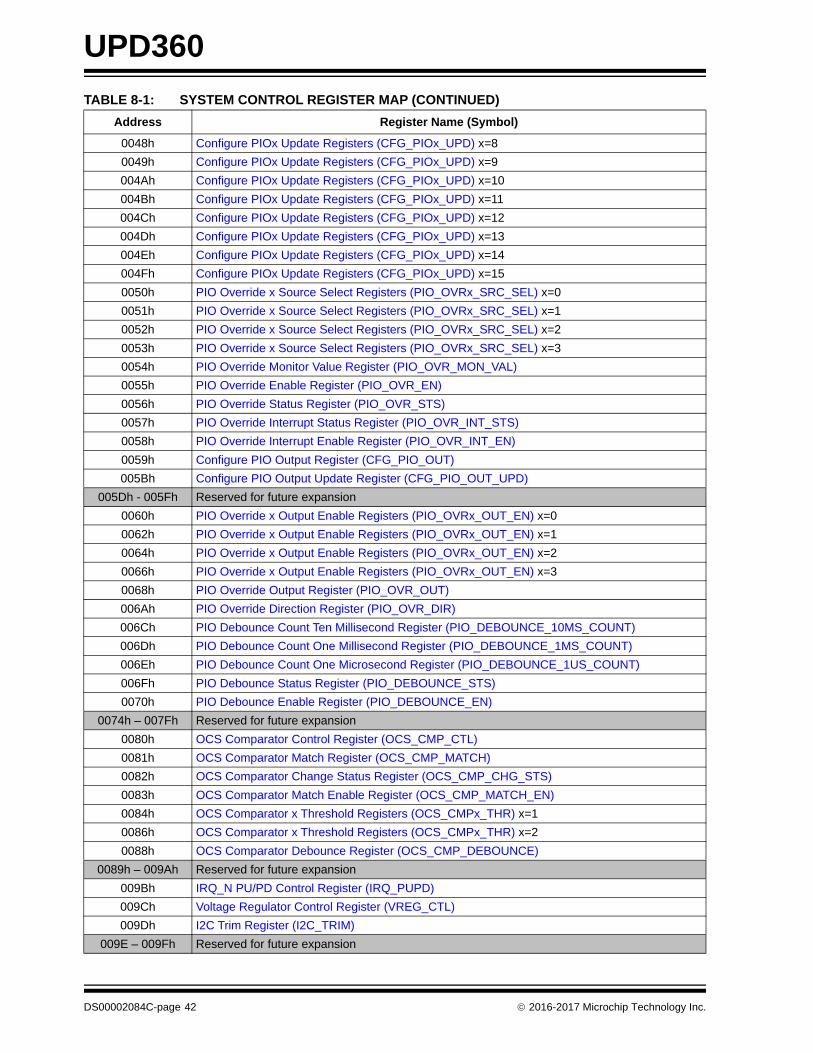
UPD360
0048h Configure PIOx Update Registers (CFG_PIOx_UPD) x=8
0049h Configure PIOx Update Registers (CFG_PIOx_UPD) x=9
004Ah Configure PIOx Update Registers (CFG_PIOx_UPD) x=10
004Bh Configure PIOx Update Registers (CFG_PIOx_UPD) x=11
004Ch Configure PIOx Update Registers (CFG_PIOx_UPD) x=12
004Dh Configure PIOx Update Registers (CFG_PIOx_UPD) x=13
004Eh Configure PIOx Update Registers (CFG_PIOx_UPD) x=14
004Fh Configure PIOx Update Registers (CFG_PIOx_UPD) x=15
0050h PIO Override x Source Select Registers (PIO_OVRx_SRC_SEL) x=0
0051h PIO Override x Source Select Registers (PIO_OVRx_SRC_SEL) x=1
0052h PIO Override x Source Select Registers (PIO_OVRx_SRC_SEL) x=2
0053h PIO Override x Source Select Registers (PIO_OVRx_SRC_SEL) x=3
0054h PIO Override Monitor Value Register (PIO_OVR_MON_VAL)
0055h PIO Override Enable Register (PIO_OVR_EN)
0056h PIO Override Status Register (PIO_OVR_STS)
0057h PIO Override Interrupt Status Register (PIO_OVR_INT_STS)
0058h PIO Override Interrupt Enable Register (PIO_OVR_INT_EN)
0059h Configure PIO Output Register (CFG_PIO_OUT)
005Bh Configure PIO Output Update Register (CFG_PIO_OUT_UPD)
005Dh - 005Fh Reserved for future expansion
0060h PIO Override x Output Enable Registers (PIO_OVRx_OUT_EN) x=0
0062h PIO Override x Output Enable Registers (PIO_OVRx_OUT_EN) x=1
0064h PIO Override x Output Enable Registers (PIO_OVRx_OUT_EN) x=2
0066h PIO Override x Output Enable Registers (PIO_OVRx_OUT_EN) x=3
0068h PIO Override Output Register (PIO_OVR_OUT)
006Ah PIO Override Direction Register (PIO_OVR_DIR)
006Ch PIO Debounce Count Ten Millisecond Register (PIO_DEBOUNCE_10MS_COUNT)
006Dh PIO Debounce Count One Millisecond Register (PIO_DEBOUNCE_1MS_COUNT)
006Eh PIO Debounce Count One Microsecond Register (PIO_DEBOUNCE_1US_COUNT)
006Fh PIO Debounce Status Register (PIO_DEBOUNCE_STS)
0070h PIO Debounce Enable Register (PIO_DEBOUNCE_EN)
0074h – 007Fh Reserved for future expansion
0080h OCS Comparator Control Register (OCS_CMP_CTL)
0081h OCS Comparator Match Register (OCS_CMP_MATCH)
0082h OCS Comparator Change Status Register (OCS_CMP_CHG_STS)
0083h OCS Comparator Match Enable Register (OCS_CMP_MATCH_EN)
0084h OCS Comparator x Threshold Registers (OCS_CMPx_THR) x=1
0086h OCS Comparator x Threshold Registers (OCS_CMPx_THR) x=2
0088h OCS Comparator Debounce Register (OCS_CMP_DEBOUNCE)
0089h – 009Ah Reserved for future expansion
009Bh IRQ_N PU/PD Control Register (IRQ_PUPD)
009Ch Voltage Regulator Control Register (VREG_CTL)
009Dh I2C Trim Register (I2C_TRIM)
009E – 009Fh Reserved for future expansion
TABLE 8-1: SYSTEM CONTROL REGISTER MAP (CONTINUED)
Address Register Name (Symbol)
DS00002084C-page 42 2016-2017 Microchip Technology Inc.

UPD360
8.5.1 DEVICE ID REGISTER (ID_REV)
Note 8-1 The default value of this field is dependent on the silicon revision of the device.
ID_REV[7:0] = 00h
ID_REV[15:8] = 01h
ID_REV[23:16] = 02h
ID_REV[31:24] = 03h
8.5.2 USB VENDOR ID REGISTER (VID)
VID[7:0] = 04h
VID[15:8] = 05h
8.5.3 USB PRODUCT ID REGISTER (PID)
PID[7:0] = 06h
PID[15:8] = 07h
00A0h General Purpose Timer Load Register (GP_TIMER_LOAD)
00A2h General Purpose Timer Interrupt Source Register (GP_TIMER_INT_SRC)
00A3h General Purpose Timer Control Register (GP_TIMER_CTL)
00A4h General Purpose Timer Count Register (GP_TIMER_COUNT)
00A6h – 03FFh Reserved for future expansion
Note: RESERVED address space must not be written under any circumstances. Failure to heed this warn-ing may result in untoward operation and unexpected results.
Address: 0000h Size: 32 bits
Bits Description Type Default
31:16 Device ID (ID) RO 0360h
15:0 Device Revision (REV) RO Note 8-1
Address: 0004h Size: 16 bits
Bits Description Type Default
15:0 USB Vendor Identification (VID) R/W 0424h
Address: 0006h Size: 16 bits
Bits Description Type Default
15:0 USB Product Identification (PID) R/W 0360h
TABLE 8-1: SYSTEM CONTROL REGISTER MAP (CONTINUED)
Address Register Name (Symbol)
2016-2017 Microchip Technology Inc. DS00002084C-page 43
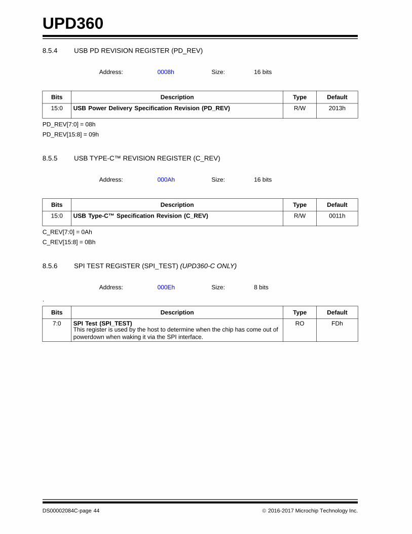
UPD360
8.5.4 USB PD REVISION REGISTER (PD_REV)
PD_REV[7:0] = 08h
PD_REV[15:8] = 09h
8.5.5 USB TYPE-C™ REVISION REGISTER (C_REV)
C_REV[7:0] = 0Ah
C_REV[15:8] = 0Bh
8.5.6 SPI TEST REGISTER (SPI_TEST) (UPD360-C ONLY)
.
Address: 0008h Size: 16 bits
Bits Description Type Default
15:0 USB Power Delivery Specification Revision (PD_REV) R/W 2013h
Address: 000Ah Size: 16 bits
Bits Description Type Default
15:0 USB Type-C™ Specification Revision (C_REV) R/W 0011h
Address: 000Eh Size: 8 bits
Bits Description Type Default
7:0 SPI Test (SPI_TEST)This register is used by the host to determine when the chip has come out of powerdown when waking it via the SPI interface.
RO FDh
DS00002084C-page 44 2016-2017 Microchip Technology Inc.
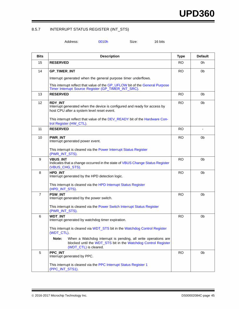
UPD360
8.5.7 INTERRUPT STATUS REGISTER (INT_STS)
Address: 0010h Size: 16 bits
Bits Description Type Default
15 RESERVED RO 0h
14 GP_TIMER_INT
Interrupt generated when the general purpose timer underflows.
This interrupt reflect that value of the GP_UFLOW bit of the General Purpose Timer Interrupt Source Register (GP_TIMER_INT_SRC).
RO 0b
13 RESERVED RO 0b
12 RDY_INTInterrupt generated when the device is configured and ready for access by host CPU after a system level reset event.
This interrupt reflect that value of the DEV_READY bit of the Hardware Con-trol Register (HW_CTL).
RO 0b
11 RESERVED RO -
10 PWR_INTInterrupt generated power event.
This interrupt is cleared via the Power Interrupt Status Register (PWR_INT_STS).
RO 0b
9 VBUS_INTIndicates that a change occurred in the state of VBUS Change Status Register (VBUS_CHG_STS).
RO 0b
8 HPD_INTInterrupt generated by the HPD detection logic.
This interrupt is cleared via the HPD Interrupt Status Register (HPD_INT_STS).
RO 0b
7 PSW_INTInterrupt generated by the power switch.
This interrupt is cleared via the Power Switch Interrupt Status Register (PWR_INT_STS).
RO 0b
6 WDT_INTInterrupt generated by watchdog timer expiration.
This interrupt is cleared via WDT_STS bit in the Watchdog Control Register (WDT_CTL).
Note: When a Watchdog interrupt is pending, all write operations areblocked until the WDT_STS bit in the Watchdog Control Register(WDT_CTL) is cleared.
RO 0b
5 PPC_INTInterrupt generated by PPC.
This interrupt is cleared via the PPC Interrupt Status Register 1 (PPC_INT_STS1).
RO 0b
2016-2017 Microchip Technology Inc. DS00002084C-page 45

UPD360
INT_STS[7:0] = 10h
INT_STS[15:8] = 11h
4 MAC_INTInterrupt generated by the PD MAC.
This interrupt is cleared via the corresponding PD MAC interrupt register, as detailed in Section 11.4.3, "PD MAC Interrupt Status and Enable Registers," on page 153.
RO 0b
3 OCS_CMP_INTInterrupt generated from the detection of an over-current condition.
This interrupt is cleared via OCS Comparator Change Status Register (OCS_CMP_CHG_STS).
RO 0b
2 PIO_OVERRIDE_INTInterrupt generated from a PIO override.
This interrupt is cleared via the PIO Override Interrupt Status Register (PIO_OVR_INT_STS).
RO 0b
1 PIO_INTInterrupt generated from configured PIO status change.
This interrupt is cleared via the PIO Interrupt Status Register (PIO_INT_STS).
RO 0b
0 CC_INTInterrupt generated by Cable Plug Orientation and Detection module.
This interrupt is cleared via the CC Interrupt Status Register (CC_INT_STS).
RO 0b
Bits Description Type Default
DS00002084C-page 46 2016-2017 Microchip Technology Inc.

UPD360
8.5.8 INTERRUPT ENABLE REGISTER (INT_EN)
INT_EN[7:0] = 12h
INT_EN[15:8] = 13h
Address: 0014h Size: 16 bits
Bits Description Type Default
15 RESERVED RO 0h
14 Interrupt Enable 13When “0”, prevents generation of the respective interrupt.
R/W 0b
13 RESERVED RO -
12 Interrupt Enable 12When “0”, prevents generation of the respective interrupt.
R/W 1b
11 RESERVED RO -
10 Interrupt Enable 10When “0”, prevents generation of the respective interrupt.
R/W 0b
9 Interrupt Enable 9When “0”, prevents generation of the respective interrupt.
R/W 0b
8 Interrupt Enable 8When “0”, prevents generation of the respective interrupt.
R/W 0b
7 Interrupt Enable 7When “0”, prevents generation of the respective interrupt.
R/W 0b
6 Interrupt Enable 6When “0”, prevents generation of the respective interrupt.
R/W 1b
5 Interrupt Enable 5When “0”, prevents generation of the respective interrupt.
R/W 0b
4 Interrupt Enable 4When “0”, prevents generation of the respective interrupt.
R/W 0b
3 Interrupt Enable 3When “0”, prevents generation of the respective interrupt.
R/W 0b
2 Interrupt Enable 2When “0”, prevents generation of the respective interrupt.
R/W 0b
1 Interrupt Enable 1When “0”, prevents generation of the respective interrupt.
R/W 0b
0 Interrupt Enable 0When “0”, prevents generation of the respective interrupt.
R/W 0b
2016-2017 Microchip Technology Inc. DS00002084C-page 47

UPD360
8.5.9 HARDWARE CONTROL REGISTER (HW_CTL)
8.5.10 I2C SLAVE ADDRESS REGISTER (I2C_ADDR) (UPD360-A/UPD360-B ONLY)
Note 8-2 The default value for this register is defined by the CFG_SEL1 pin.
Address: 0018h Size: 16 bits
Bits Description Type Default
15:6 RESERVED RO -
5 I2C_GEN_CALL_EN
0: I2C General Call address not supported.1: I2C General Call address supported.
R/W 0b
4 RESERVED RO -
3 I2C FMPLUSWhen set, this bit configures the I2C interface to operate in fast-mode plus mode.
Note: UPD360-A/UPD360-B only.
R/W 1b
2 DEV_READYWhen set, this bit indicates that the device has been fully configured after a system level reset event.
R/SC 0b
1 PIO_UPD_REQWhen this bit is set, the PIO registers are updated from the respective simultaneous update registers.
After the operation completes, this bit is automatically cleared.
The request will not be accepted if an override function is pending. After the override condition is cleared by software, the update request will be accepted. The override is cleared via respective bit of PIO Override Enable Register (PIO_OVR_EN).
R/SC 0b
0 SRESETSoftware reset. When set this bit initiates a chip level reset.
SC 0b
Address: 001Ah Size: 8 bits
Bits Description Type Default
7 RESERVED RO -
6:0 I2C Slave AddressDefines the slave address used by the I2C controller.
R/W Note 8-2
DS00002084C-page 48 2016-2017 Microchip Technology Inc.

UPD360
8.5.11 PPC STATUS REGISTER (PPC_BUSY)
.
8.5.12 PIO STATUS REGISTER (PIO_STS)
Address: 001Bh Size: 8 bits
BITS DESCRIPTION TYPE DEFAULT
7:1 RESERVED RO -
0 PPC_BUSY
This bit is used to indicate when the PPC is processing a register write request. 0b: PPC is not busy processing a register write access. A new register write may be initiated.
1b: PPC is processing a register write access. A new register write may not be initiated until this bit clears.
RO 0b
Address: 0020h Size: 16 bits
Bits Description Type Default
15 PIO150b: PIO is low1b: PIO is high
RO 0b
14 PIO140b: PIO is low1b: PIO is high
RO 0b
13 PIO130b: PIO is low1b: PIO is high
RO 0b
12 PIO120b: PIO is low1b: PIO is high
RO 0b
11 PIO110b: PIO is low1b: PIO is high
RO 0b
10 PIO100b: PIO is low1b: PIO is high
RO 0b
9 PIO90b: PIO is low1b: PIO is high
RO 0b
8 PIO80b: PIO is low1b: PIO is high
RO 0b
7 PIO70b: PIO is low1b: PIO is high
RO 0b
2016-2017 Microchip Technology Inc. DS00002084C-page 49
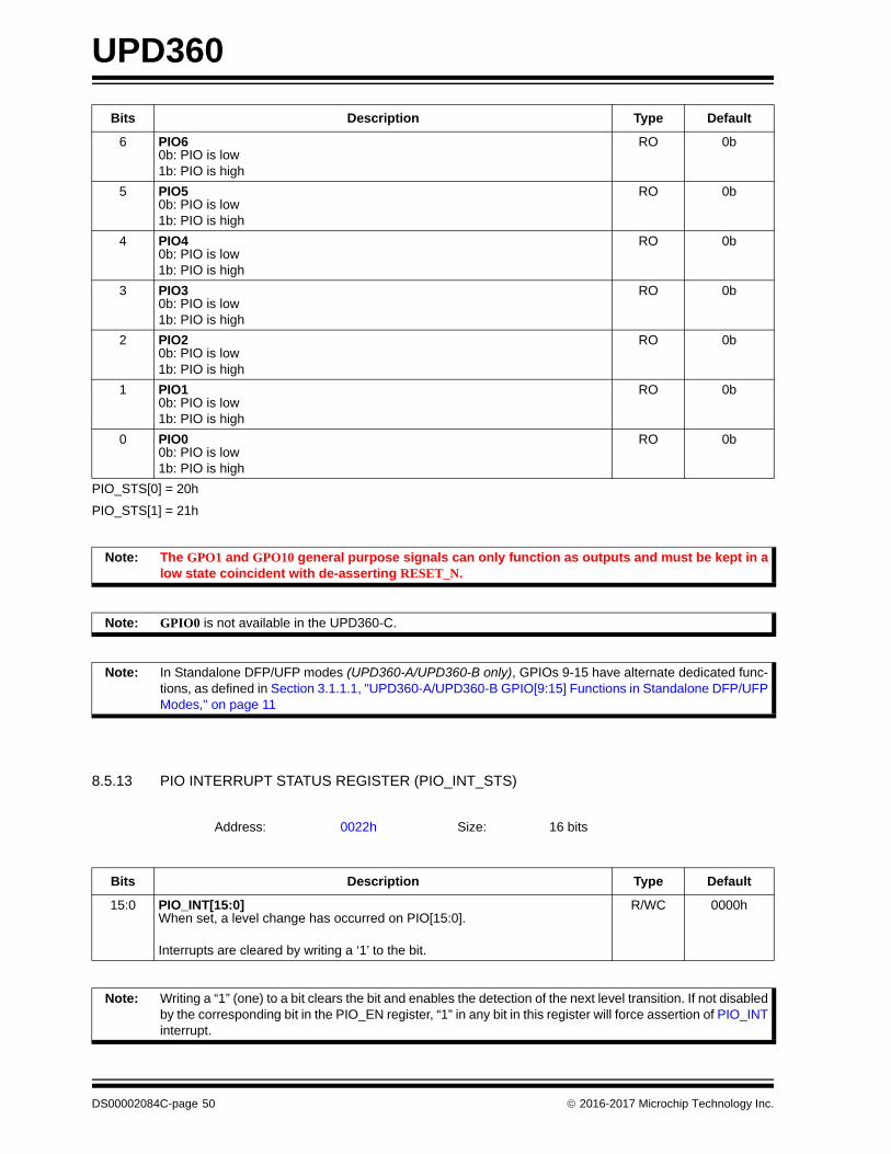
UPD360
PIO_STS[0] = 20h
PIO_STS[1] = 21h
8.5.13 PIO INTERRUPT STATUS REGISTER (PIO_INT_STS)
6 PIO60b: PIO is low1b: PIO is high
RO 0b
5 PIO50b: PIO is low1b: PIO is high
RO 0b
4 PIO40b: PIO is low1b: PIO is high
RO 0b
3 PIO30b: PIO is low1b: PIO is high
RO 0b
2 PIO20b: PIO is low1b: PIO is high
RO 0b
1 PIO10b: PIO is low1b: PIO is high
RO 0b
0 PIO00b: PIO is low1b: PIO is high
RO 0b
Note: The GPO1 and GPO10 general purpose signals can only function as outputs and must be kept in alow state coincident with de-asserting RESET_N.
Note: GPIO0 is not available in the UPD360-C.
Note: In Standalone DFP/UFP modes (UPD360-A/UPD360-B only), GPIOs 9-15 have alternate dedicated func-tions, as defined in Section 3.1.1.1, "UPD360-A/UPD360-B GPIO[9:15] Functions in Standalone DFP/UFPModes," on page 11
Address: 0022h Size: 16 bits
Bits Description Type Default
15:0 PIO_INT[15:0]When set, a level change has occurred on PIO[15:0].
Interrupts are cleared by writing a ‘1’ to the bit.
R/WC 0000h
Note: Writing a “1” (one) to a bit clears the bit and enables the detection of the next level transition. If not disabledby the corresponding bit in the PIO_EN register, “1” in any bit in this register will force assertion of PIO_INTinterrupt.
Bits Description Type Default
DS00002084C-page 50 2016-2017 Microchip Technology Inc.
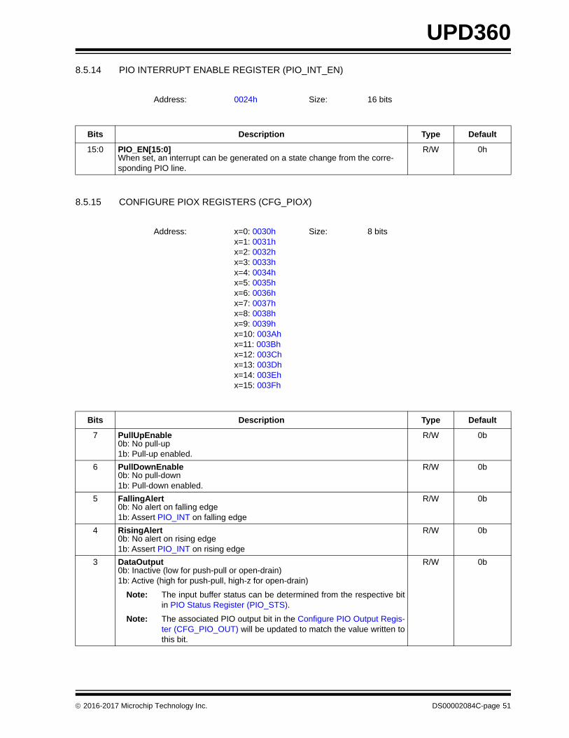
UPD360
8.5.14 PIO INTERRUPT ENABLE REGISTER (PIO_INT_EN)
8.5.15 CONFIGURE PIOX REGISTERS (CFG_PIOX)
Address: 0024h Size: 16 bits
Bits Description Type Default
15:0 PIO_EN[15:0]When set, an interrupt can be generated on a state change from the corre-sponding PIO line.
R/W 0h
Address: x=0: 0030hx=1: 0031hx=2: 0032hx=3: 0033hx=4: 0034hx=5: 0035hx=6: 0036hx=7: 0037hx=8: 0038hx=9: 0039hx=10: 003Ahx=11: 003Bhx=12: 003Chx=13: 003Dhx=14: 003Ehx=15: 003Fh
Size: 8 bits
Bits Description Type Default
7 PullUpEnable0b: No pull-up1b: Pull-up enabled.
R/W 0b
6 PullDownEnable0b: No pull-down1b: Pull-down enabled.
R/W 0b
5 FallingAlert0b: No alert on falling edge1b: Assert PIO_INT on falling edge
R/W 0b
4 RisingAlert0b: No alert on rising edge1b: Assert PIO_INT on rising edge
R/W 0b
3 DataOutput0b: Inactive (low for push-pull or open-drain)1b: Active (high for push-pull, high-z for open-drain)
Note: The input buffer status can be determined from the respective bitin PIO Status Register (PIO_STS).
Note: The associated PIO output bit in the Configure PIO Output Regis-ter (CFG_PIO_OUT) will be updated to match the value written tothis bit.
R/W 0b
2016-2017 Microchip Technology Inc. DS00002084C-page 51
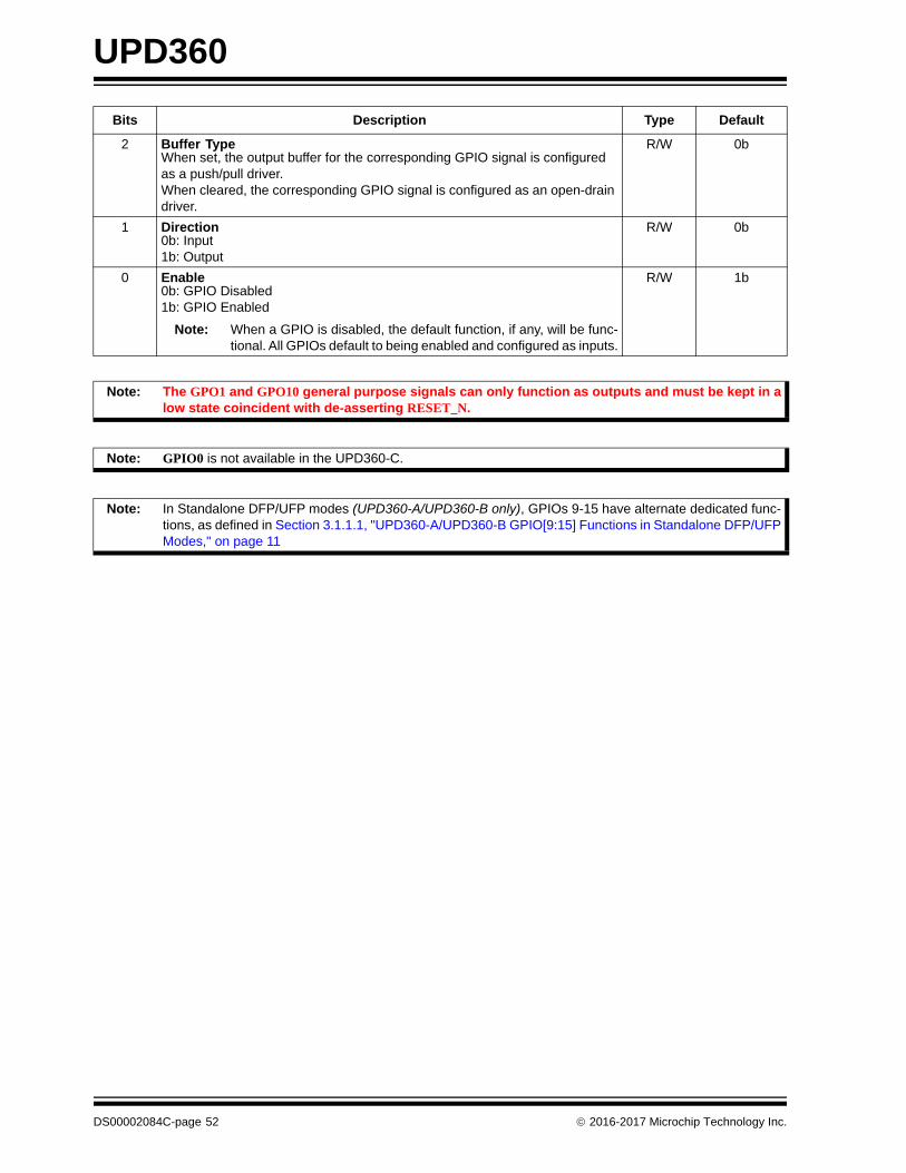
UPD360
2 Buffer TypeWhen set, the output buffer for the corresponding GPIO signal is configured as a push/pull driver. When cleared, the corresponding GPIO signal is configured as an open-drain driver.
R/W 0b
1 Direction0b: Input1b: Output
R/W 0b
0 Enable0b: GPIO Disabled1b: GPIO Enabled
Note: When a GPIO is disabled, the default function, if any, will be func-tional. All GPIOs default to being enabled and configured as inputs.
R/W 1b
Note: The GPO1 and GPO10 general purpose signals can only function as outputs and must be kept in alow state coincident with de-asserting RESET_N.
Note: GPIO0 is not available in the UPD360-C.
Note: In Standalone DFP/UFP modes (UPD360-A/UPD360-B only), GPIOs 9-15 have alternate dedicated func-tions, as defined in Section 3.1.1.1, "UPD360-A/UPD360-B GPIO[9:15] Functions in Standalone DFP/UFPModes," on page 11
Bits Description Type Default
DS00002084C-page 52 2016-2017 Microchip Technology Inc.
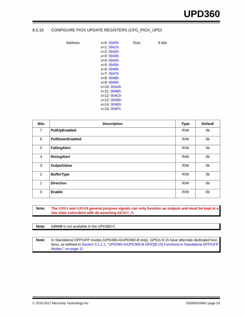
UPD360
8.5.16 CONFIGURE PIOX UPDATE REGISTERS (CFG_PIOX_UPD)
Address: x=0: 0040hx=1: 0041hx=2: 0042hx=3: 0043hx=4: 0044hx=5: 0045hx=6: 0046hx=7: 0047hx=8: 0048hx=9: 0049hx=10: 004Ahx=11: 004Bhx=12: 004Chx=13: 004Dhx=14: 004Ehx=15: 004Fh
Size: 8 bits
Bits Description Type Default
7 PullUpEnabled R/W 0b
6 PullDownEnabled R/W 0b
5 FallingAlert R/W 0b
4 RisingAlert R/W 0b
3 OutputValue R/W 0b
2 BufferType R/W 0b
1 Direction R/W 0b
0 Enable R/W 0b
Note: The GPO1 and GPO10 general purpose signals can only function as outputs and must be kept in alow state coincident with de-asserting RESET_N.
Note: GPIO0 is not available in the UPD360-C.
Note: In Standalone DFP/UFP modes (UPD360-A/UPD360-B only), GPIOs 9-15 have alternate dedicated func-tions, as defined in Section 3.1.1.1, "UPD360-A/UPD360-B GPIO[9:15] Functions in Standalone DFP/UFPModes," on page 11
2016-2017 Microchip Technology Inc. DS00002084C-page 53
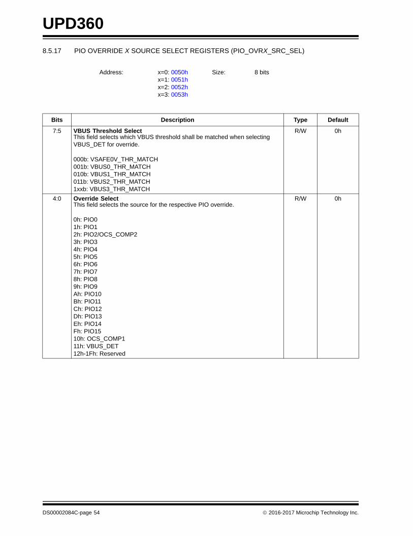
UPD360
8.5.17 PIO OVERRIDE X SOURCE SELECT REGISTERS (PIO_OVRX_SRC_SEL)
Address: x=0: 0050hx=1: 0051hx=2: 0052hx=3: 0053h
Size: 8 bits
Bits Description Type Default
7:5 VBUS Threshold SelectThis field selects which VBUS threshold shall be matched when selecting VBUS_DET for override.
000b: VSAFE0V_THR_MATCH001b: VBUS0_THR_MATCH010b: VBUS1_THR_MATCH011b: VBUS2_THR_MATCH1xxb: VBUS3_THR_MATCH
R/W 0h
4:0 Override SelectThis field selects the source for the respective PIO override.
0h: PIO01h: PIO12h: PIO2/OCS_COMP23h: PIO34h: PIO45h: PIO56h: PIO67h: PIO78h: PIO89h: PIO9Ah: PIO10Bh: PIO11Ch: PIO12Dh: PIO13Eh: PIO14Fh: PIO1510h: OCS_COMP111h: VBUS_DET12h-1Fh: Reserved
R/W 0h
DS00002084C-page 54 2016-2017 Microchip Technology Inc.

UPD360
8.5.18 PIO OVERRIDE MONITOR VALUE REGISTER (PIO_OVR_MON_VAL)
8.5.19 PIO OVERRIDE ENABLE REGISTER (PIO_OVR_EN)
Address: 0054h Size: 8 bits
Bits Description Type Default
7:4 RESERVED RO -
3 PIO_MON_VAL3Override function 3 monitors for this value on the selected PIO.
R/W 0b
2 PIO_MON_VAL2Override function 2 monitors for this value on the selected PIO.
R/W 0b
1 PIO_MON_VAL1Override function 1 monitors for this value on the selected PIO.
R/W 0b
0 PIO_MON_VAL0Override function 0 monitors for this value on the selected PIO.
R/W 0b
Note: When the PIO is mapped to an OCS comparator or VBUS comparator, the monitored case is rising above/falling below the associated threshold. Setting the override monitor value indicates that the source exceed-ing the threshold is monitored. If the value is cleared then being below the threshold is monitored.
Address: 0055h Size: 8 bits
Bits Description Type Default
7:4 RESERVED RO -
3 PIO_OVR_EN3When set PIO Override 3 is enabled.
R/W 0b
2 PIO_OVR_EN2When set PIO Override 2 is enabled.
R/W 0b
1 PIO_OVR_EN1When set PIO Override 1 is enabled.
R/W 0b
0 PIO_OVR_EN0When set PIO Override 0 is enabled.
R/W 0b
2016-2017 Microchip Technology Inc. DS00002084C-page 55

UPD360
8.5.20 PIO OVERRIDE STATUS REGISTER (PIO_OVR_STS)
Address: 0056h Size: 8 bits
Bits Description Type Default
7:4 RESERVED RO -
3 PIO_OVR_STS3Override function is active on the selected PIO.
Set on a match to PIO_MON_VAL3 and clears on override feature disable PIO_OVR_EN3 =0.
RO 0b
2 PIO_OVR_STS2Override function is active on the selected PIO.
Set on a match to PIO_MON_VAL2 and clears on override feature disable PIO_OVR_EN2 =0.
RO 0b
1 PIO_OVR_STS1Override function is active on the selected PIO.
Set on a match to PIO_MON_VAL1 and clears on override feature disable PIO_OVR_EN1 =0.
RO 0b
0 PIO_OVR_STS0Override function is active on the selected PIO.
Set on a match to PIO_MON_VAL0 and clears on override feature disable PIO_OVR_EN0 =0.
RO 0b
DS00002084C-page 56 2016-2017 Microchip Technology Inc.
UPD360
8.5.21 PIO OVERRIDE INTERRUPT STATUS REGISTER (PIO_OVR_INT_STS)
8.5.22 PIO OVERRIDE INTERRUPT ENABLE REGISTER (PIO_OVR_INT_EN)
Address: 0057h Size: 8 bits
Bits Description Type Default
7:4 RESERVED RO -
3 PIO_OVR_INTR3This interrupt is set when override function 3 detects the programmed moni-tored value on the selected PIO.
The interrupt persists until cleared.
R/WC 0b
2 PIO_OVR_INTR2This interrupt is set when override function 2 detects the programmed moni-tored value on the selected PIO.
The interrupt persists until cleared.
R/WC 0b
1 PIO_OVR_INTR1This interrupt is set when override function 1 detects the programmed moni-tored value on the selected PIO.
The interrupt persists until cleared.
R/WC 0b
0 PIO_OVR_INTR0This interrupt is set when override function 0 detects the programmed moni-tored value on the selected PIO.
The interrupt persists until cleared.
R/WC 0b
Address: 0058h Size: 8 bits
Bits Description Type Default
7:4 RESERVED RO 0h
3 PIO_OVR_INTR3When ‘1’, enables the generation of this interrupt.
R/W 0b
2 PIO_OVR_INTR2When ‘1’, enables the generation of this interrupt.
R/W 0b
1 PIO_OVR_INTR1When ‘1’, enables the generation of this interrupt.
R/W 0b
0 PIO_OVR_INTR0When ‘1’, enables the generation of this interrupt.
R/W 0b
2016-2017 Microchip Technology Inc. DS00002084C-page 57

UPD360
8.5.23 CONFIGURE PIO OUTPUT REGISTER (CFG_PIO_OUT)
This register enables multiple PIO output values to be updated in a single CSR write.
8.5.24 CONFIGURE PIO OUTPUT UPDATE REGISTER (CFG_PIO_OUT_UPD)
8.5.25 PIO OVERRIDE X OUTPUT ENABLE REGISTERS (PIO_OVRX_OUT_EN)
Address: 0059h Size: 16 bits
Bits Description Type Default
15:0 CFG_PIO_OUTWhen this register is written, the output values for the respective PIOs are updated. Specifically, the DataOutput in the respective CFG_PIOx registers are updated.
This register is not updated until the byte located at 005Ah is written by soft-ware. This is to prevent placing externally driven components in an invalid state while updating.
R/W 0000h
Address: 005Bh Size: 16 bits
Bits Description Type Default
15:0 CFG_PIO_OUTx_UPD R/W 0000h
Address: x=0: 0060hx=1: 0062hx=2: 0064hx=3: 0066h
Size: 16 bits
Bits Description Type Default
15:0 PIO_OVR_OUT_EN_XEach of the overrides has an instance of this CSR to indicate which PIO out-puts are controlled by it. When asserted associated PIO output’s state is con-trolled by the respective override function.
Note: The same PIO output can be enabled by multiple overrides.
R/W 0h
DS00002084C-page 58 2016-2017 Microchip Technology Inc.
UPD360
8.5.26 PIO OVERRIDE OUTPUT REGISTER (PIO_OVR_OUT)
8.5.27 PIO OVERRIDE DIRECTION REGISTER (PIO_OVR_DIR)
8.5.28 PIO DEBOUNCE COUNT TEN MILLISECOND REGISTER (PIO_DEBOUNCE_10MS_COUNT)
Address: 0068h Size: 16 bits
Bits Description Type Default
15:0 PIO Override OutputThis field defines the PIO output value to be used when the respective PIO is enabled for override and the associated override is triggered.
R/W 0h
Address: 006Ah Size: 16 bits
Bits Description Type Default
15:0 PIO Override DirectionThis field defines the PIO direction value to be used when the respective PIO is enabled for override and the associated override is triggered.
R/W 0h
Address: 006Ch Size: 8 bits
Bits Description Type Default
7:0 PIO_DEBOUNCE_10MS_COUNTThis register holds the 10 ms debounce counter.
Any transition within the debounce period is suppressed. Each count corre-sponds to 10 ms, with the default value being 100 ms.
This register is used when the debounce granularity is 10 ms.
Note: The actual count may be either count or count-1.
R/W 0Ah
2016-2017 Microchip Technology Inc. DS00002084C-page 59

UPD360
8.5.29 PIO DEBOUNCE COUNT ONE MILLISECOND REGISTER (PIO_DEBOUNCE_1MS_COUNT)
8.5.30 PIO DEBOUNCE COUNT ONE MICROSECOND REGISTER (PIO_DEBOUNCE_1US_COUNT)
Address: 006Dh Size: 8 bits
Bits Description Type Default
7:0 PIO_DEBOUNCE_1MS_COUNTThis register holds the 1 ms debounce counter.
Any transition within the debounce period is suppressed. Each count corre-sponds to 1 ms, with the default value being 10 ms.
This register is used when the debounce granularity is 1 ms.
Note: The actual count may be either count or count-1.
R/W 0Ah
Address: 006Eh Size: 8 bits
Bits Description Type Default
7:0 PIO_DEBOUNCE_1US_COUNTThis register holds the 1 us debounce counter.
Any transition within the debounce period is suppressed. Each count corre-sponds to 1 us, with the default value being 10 us.
This register is used when the debounce granularity is 1 us.
Note: The actual count may be either count or count-1.
R/W 0Ah
DS00002084C-page 60 2016-2017 Microchip Technology Inc.

UPD360
8.5.31 PIO DEBOUNCE STATUS REGISTER (PIO_DEBOUNCE_STS)
8.5.32 PIO DEBOUNCE ENABLE REGISTER (PIO_DEBOUNCE_EN)
This register enables a PIO for debouncing and selects the debouncer to be used as defined below:
• 00b: Debounce disabled
• 01b: Debounce Enabled (PIO Debounce Count One Microsecond Register (PIO_DEBOUNCE_1US_COUNT))
• 10b: Debounce Enabled (PIO Debounce Count One Millisecond Register (PIO_DEBOUNCE_1MS_COUNT))
• 11b: Debounce Enabled (PIO Debounce Count Ten Millisecond Register (PIO_DEBOUNCE_10MS_COUNT))
Address: 006Fh Size: 8 bits
Bits Description Type Default
7:1 RESERVED RO 0h
0 PIO_DB_ACTPIO Debounce Active
This bit is used to indicate that a PIO debounce is in process.1b: PIO debounce pending0b: PIO not pending
RO 0b
Address: 0070h Size: 32 bits
Bits Description Type Default
31:30 PIO_DB_EN15 R/W 00b
29:28 PIO_DB_EN14 R/W 00b
27:26 PIO_DB_EN13 R/W 00b
25:24 PIO_DB_EN12 R/W 00b
23:22 PIO_DB_EN11 R/W 00b
21:20 PIO_DB_EN10 R/W 00b
19:18 PIO_DB_EN9 R/W 00b
17:16 PIO_DB_EN8 R/W 00b
15:14 PIO_DB_EN7 R/W 00b
13:12 PIO_DB_EN6 R/W 00b
11:10 PIO_DB_EN5 R/W 00b
9:8 PIO_DB_EN4 R/W 00b
7:6 PIO_DB_EN3 R/W 00b
2016-2017 Microchip Technology Inc. DS00002084C-page 61

UPD360
8.5.33 OCS COMPARATOR CONTROL REGISTER (OCS_CMP_CTL)
8.5.34 OCS COMPARATOR MATCH REGISTER (OCS_CMP_MATCH)
This bit is always cleared when OCS Comparator Control is not enabled for the respective OCS_COMP pin.
5:4 PIO_DB_EN2 R/W 00b
3:2 PIO_DB_EN1 R/W 00b
1:0 PIO_DB_EN0 R/W 00b
Note: GPIO0 is not available in the UPD360-C.
Address: 0080h Size: 8 bits
Bits Description Type Default
7 OCS_DB_ACTIVEWhen this bit reads back 0b, the debouncer is disabled. The OCS debouncer is enabled when it reads back 1b.
RO 0b
6:2 RESERVED RO 0h
1:0 OCS Comparator Control00b: OCS Comparator and DAC are powered down01b: OCS Comparator samples OCS_COMP110b: OCS Comparator samples OCS_COMP211b: OCS Comparator samples OCS_COMP1 and OCS_COMP2
When set to 01b or 10b, a sample is taken every 100 us. When set to 11b, each OCS_COMPx pin is effectively sampled every 200 us.
R/W 00b
Address: 0081h Size: 8 bits
Bits Description Type Default
7:2 RESERVED RO 0h
1 OCS Comparator Match 2When set, this bit indicates that a match has occurred and an OCS condition has been detected on OCS_COMP2 pin.
RO 0b
0 OCS Comparator Match 1When set, this bit indicates that a match has occurred and an OCS condition has been detected on OCS_COMP1 pin.
RO 0b
Bits Description Type Default
DS00002084C-page 62 2016-2017 Microchip Technology Inc.
UPD360
8.5.35 OCS COMPARATOR CHANGE STATUS REGISTER (OCS_CMP_CHG_STS)
8.5.36 OCS COMPARATOR MATCH ENABLE REGISTER (OCS_CMP_MATCH_EN)
Address: 0082h Size: 8 bits
Bits Description Type Default
7:6 OCSx Match Valid (OCSx_MATCH_VLD)Asserts after the OCS debouncer is first enabled, via OCS Comparator Con-trol, and the first match becomes valid in OCS Comparator Match Register (OCS_CMP_MATCH).
Bit 7 = OCS2_MATCH_VLDBit 6 = OCS1_MATCH_VLD
R/WC 0b
5:2 RESERVED RO 0h
1:0 OCSx Change Status (OCSx_CHG_STS)When set, each bit indicates that the respective bit in OCS Comparator Match Register (OCS_CMP_MATCH) has changed.
Bit 1 = OCS2_CHG_STSBit 0 = OCS1_CHG_STS
A write of 1b clears the respective status bit.
R/WC 00b
Address: 0083h Size: 8 bits
Bits Description Type Default
7:6 OCSx Match Valid Enable (OCSx_MATCH_VLD_EN)When set, the corresponding bit in OCS Comparator Change Status Register (OCS_CMP_CHG_STS) can cause the assertion of the OCS_CMP_INT inter-rupt.
Bit 7 = OCS2_MATCH_VLD_ENBit 6 = OCS1_MATCH_VLD_EN
R/W 0b
5:2 RESERVED RO 0h
1:0 OCSx Comparator Match Enable (OCSx_CMP_MATCH_EN)When set the corresponding bit in OCS Comparator Change Status Register (OCS_CMP_CHG_STS) can cause the assertion of the OCS_CMP_INT inter-rupt.
Bit 1 = OCS2_CMP_MATCH_ENBit 0 = OCS1_CMP_MATCH_EN
R/W 00b
2016-2017 Microchip Technology Inc. DS00002084C-page 63

UPD360
8.5.37 OCS COMPARATOR X THRESHOLD REGISTERS (OCS_CMPX_THR)
8.5.38 OCS COMPARATOR DEBOUNCE REGISTER (OCS_CMP_DEBOUNCE)
8.5.39 IRQ_N PU/PD CONTROL REGISTER (IRQ_PUPD)
This register controls the PU and PU for the IRQ_N pin.
Address: x=1: 0084hx=2: 0086h
Size: 16 bits
Bits Description Type Default
15:10 RESERVED RO 0h
9:0 OCS Comparator ThresholdThe lower byte of the threshold must be written before the upper byte. The entire 10-bit threshold is updated when the second write occurs.
This has units of ~2.5V/1024.
Note: This register shall not be modified while the OCS debouncer isenabled.
R/W 0h
Address: 0088h Size: 8 bits
Bits Description Type Default
7:0 OCS_CMP_DEBOUNCEIndicates the period of time for which the OCS_COMP1 and OCS_COMP2 inputs are debounced.
This field has units of 100 us.
Note: This register shall not be modified while the OCS debouncer isenabled.
R/W 0Fh
Address: 009Bh Size: 8 bits
Bits Description Type Default
7 PullUpEnable0: No pull-up1: Pull-up enabled.
R/W 0b
6 PullDownEnable0: No pull-down1: Pull-down enabled.
R/W 0b
5:0 RESERVED RO -
DS00002084C-page 64 2016-2017 Microchip Technology Inc.

UPD360
8.5.40 VOLTAGE REGULATOR CONTROL REGISTER (VREG_CTL)
8.5.41 I2C TRIM REGISTER (I2C_TRIM)
8.5.42 GENERAL PURPOSE TIMER LOAD REGISTER (GP_TIMER_LOAD)
Address: 009Ch Size: 8 bits
Bits Description Type Default
7:1 RESERVED RO -
1 VREG_LOW_OVR
When set, the 1.8V voltage regulator is placed in low power mode whenever both the Ring Oscillator and 48MHz Relaxation Oscillator are disabled.
Note: It is expected tor this bit to be set in CPU companion mode.
Note: In standalone modes, the respective OTP bit shall be set to enable this feature and to ensure maximum power savings.
R/W 0b
0 VREG Low Power Enable (VREG_LOW_EN)When set, the 1.8V voltage regulator is placed in low power mode.
Note: This bit has no meaning when the VREG_LOW_OVR bit is set.
R/W 0b
Address: 009Dh Size: 8 bits
BITS DESCRIPTION TYPE DEFAULT
7:0 I2C_TRIMThis register specifies the delay added by the I2C controller in order to meet the tHD_DAT parameter.
This register has units of 20.8 ns.
R/W 9h
Address: 00A0h Size: 16 bits
BITS DESCRIPTION TYPE DEFAULT
15:0 GP Timer LoadThis register defines the value to be loaded into the general purpose timer from which it will count down.
The valid range for this register is 0001h - FFFFh.
This field has units of 1 ms.
Note: Programming 0h into this register is not valid.
Note: Software shall not change the contents of this register while the RESET bit is set and shall wait until this bit is cleared.
R/W FFFFh
2016-2017 Microchip Technology Inc. DS00002084C-page 65
UPD360
8.5.43 GENERAL PURPOSE TIMER INTERRUPT SOURCE REGISTER (GP_TIMER_INT_SRC)
8.5.44 GENERAL PURPOSE TIMER CONTROL REGISTER (GP_TIMER_CTL)
Address: 00A2h Size: 8 bits
BITS DESCRIPTION TYPE DEFAULT
7:1 RESERVED RO -
0 GP_UFLOWThis bit will be set when the general purpose timer underflows. The GP_TIMER_INT interrupt in Interrupt Status Register (INT_STS) persists until this bit is cleared.
When DIS_ON_UFLOW bit of the General Purpose Timer Control Register (GP_TIMER_CTL) is set, the assertion of this bit is delayed until the timer is fully disabled (100s us).
R/WC 0b
Address: 00A3h Size: 8 bits
BITS DESCRIPTION TYPE DEFAULT
7 STATUSThis bit indicates the operational state of the GP timer.
0: Timer is disabled and not counting1: Timer is enabled and counting
When this bit is cleared the timer has halted operation.
RO 0b
6:3 RESERVED RO -
2 DIS_ON_UFLOWWhen this bit is set, the GP timer is automatically disabled upon detection of the underflow condition. Additionally, the ENABLE bit is cleared upon underflow detection and the assertion of GP_UFLOW will be delayed until the GP Timer has halted operation and the STATUS bit is cleared.
R/W 0b
1 RESETTimer Reset. When set this bit stops the timer and resets the internal counter to the value in the General Purpose Timer Load Register (GP_TIMER_LOAD).
0: Timer is not in reset1: Timer is in reset
Note: This bit does not clear until propagation of the reset completes. This may take 100s us.
R/SC 0b
DS00002084C-page 66 2016-2017 Microchip Technology Inc.
UPD360
8.5.45 GENERAL PURPOSE TIMER COUNT REGISTER (GP_TIMER_COUNT)
0 ENABLETimer Enable. This bit is used to start and stop the General Purpose Timer Load Register (GP_TIMER_LOAD). This bit does not reset the timer count.
This is automatically cleared when the DIS_ON_UFLOW bit is set.
0: Timer is disabled1: Timer is enabled
R/W 0b
Address: 00A4h Size: 16 bits
BITS DESCRIPTION TYPE DEFAULT
15:0 GP Timer CounterThis register returns the current value of the general purpose timer.
The GP timer must be disabled before reading this register by clearing the ENABLE bit.
RO 0h
BITS DESCRIPTION TYPE DEFAULT
2016-2017 Microchip Technology Inc. DS00002084C-page 67
UPD360
9.0 CABLE PLUG ORIENTATION AND DETECTION
This section details the functions that control and monitor the CC pins, monitor the VBUS_DET pin, control the VCONNFETs, and sample the CFG_SEL0 and CFG_SEL1 pins.
9.1 CC Comparator
The device integrates a comparator and DAC circuit to implement Type-C attach and detach functions. It supports upto eight programmable thresholds for attach detection between UFP and DFP. When operating as a UFP, the devicesupports detecting changes in the DFP’s advertised thresholds to determine current sourcing capability. The defaultnominal values for the thresholds detected by the CC comparators are:
• 0.20 V
• 0.40 V
• 0.66 V
• 0.80 V
• 1.23 V
• 1.60 V
• 2.60 V
• 3.0 V Proprietary Mode
TABLE 9-1: CABLE DETECT SUMMARY
Parameter Threshold CSR Description Min Typ Max
DFP_ACT_DEF CC_THR0 Detecting an active cable when configured as DFP and advertising default USB current.
0.20 V
UFP_DFP_DEF CC_THR0 Detecting DFP attach when configured as UFP and DFP is advertising default USB current.
0.20 V
DFP_ACT_1A5 CC_THR1 Detecting an active cable when configured as DFP and advertising 1.5A.
0.40 V
UFP_DFP_1A5 CC_THR2 Detecting DFP attach when configured as UFP and DFP is advertising 1.5A.
0.66 V
DFP_ACT_3A0 CC_THR3 Detecting an active cable when configured as DFP and advertising 3.0A.
0.80 V
UFP_DFP_3A0 CC_THR4 Detecting DFP attach when configured as UFP and DFP is advertising 3.0A.
1.23 V
DFP_UFP_DEF CC_THR5 Detecting UFP attach when configured as DFP advertising default USB current.
1.60 V
DFP_UFP_1A5 CC_THR5 Detecting UFP attach when configured as DFP advertising 1.5A.
1.60 V
DFP_UFP_3A0 CC_THR6 Detecting UFP attach when configured as DFP advertising 3.0A.
2.60 V
DS00002084C-page 68 2016-2017 Microchip Technology Inc.
UPD360
The following tables summarize the expected thresholds to be matched in the CCx Match Registers (CCx_MATCH) forvarious configurations. Refer to the CCx Debounce Clear Enable Registers (CCx_DBCLR_EN) for the debouncer maskused in these configurations.
The following examples illustrate the rationale behind the expected matches in the previous tables.
DFP: Advertise 1.5 A and connected to powered cable, UFP not attached
In this scenario the DFP is advertising 1.5 A and connected to a powered cable. The UFP is not attached. The vRd valuemeasured will be less than 0.35V per specification.
In this configuration the following thresholds are enabled for matching:
• CC_THR1 (DFP_ACT_1A5)
TABLE 9-2: DFP CC MATCH SUMMARY
CC StateCC
THR0CC
THR1CC
THR2CC
THR3CC
THR4CC
THR5CC
THR6CC
THR7
Advertise Default USB Current and connected to powered cable
0 0 0 0 0 0 0 0
Advertise 1.5 A and connected to powered cable
0 0 0 0 0 0 0 0
Advertise 3.0 A and connected to powered cable
0 0 0 0 0 0 0 0
Advertise Default USB Current and connected to UFP
1 0 0 0 0 0 0 0
Advertise 1.5 A and connected to UFP
0 1 0 0 0 0 0 0
Advertise 3.0 A and connected to UFP
0 0 0 1 0 0 0 0
Advertise Default USB Current and no connect (vOpen)
1 0 0 0 0 1 0 0
Advertise 1.5 A and no connect (vOpen)
0 1 0 0 0 1 0 0
Advertise 3.0 A and no connect (vOpen)
0 0 0 1 0 0 1 0
Proprietary Mode and no connect (vOpen)
0 0 0 0 0 0 0 1
TABLE 9-3: UFP CC MATCH SUMMARY
CC StateCC
THR0CC_
THR1CC
THR2CC
THR3CC
THR4CC
THR5CC
THR6CC
THR7
Powered cable detected. 0 0 0 0 0 0 0 0
No Connect (SNK.Open) 0 0 0 0 0 0 0 0
DFP Connected and advertising default USB current
1 0 0 0 0 0 0 0
DFP Connected and advertising 1.5 A
1 0 1 0 0 0 0 0
DFP Connected and advertising 3.0 A
1 0 1 0 1 0 0 0
DFP Connected and advertising pro-prietary current
1 0 1 0 1 0 0 1
2016-2017 Microchip Technology Inc. DS00002084C-page 69

UPD360
• CC_THR5 (DFP_UFP_1A5)
The value programmed into CCx Debounce Clear Enable Registers (CCx_DBCLR_EN) and CCx Match Enable Regis-ters (CCx_MATCH_EN) would therefore be 0x22.
Since the vRd is less than 0.35V no threshold matches would be detected on CCx Match Registers (CCx_MATCH) orCCx Change Status Registers (CCx_CHG_STS).
DFP: Advertise 3.0 A and connected to UFP
In this scenario the DFP is advertising 3.0 A and connected to a UFP. The vRd value measured will be > 0.85V and <2.45V.
In this configuration the following thresholds are enabled for matching:
• CC_THR3 (DFP_ACT_3A0)
• CC_THR6 (DFP_UFP_3A0)
The value programmed into CCx Debounce Clear Enable Registers (CCx_DBCLR_EN) and CCx Match Enable Regis-ters (CCx_MATCH_EN) would therefore be 0x44.
In this case only CC_THR3 would be matched. Bit 3 would be set in both CCx Match Registers (CCx_MATCH) or CCxChange Status Registers (CCx_CHG_STS) after the debounce interval.
UFP: Connected to DFP advertising 3.0 A
In this case the UFP is connected to a DFP advertising 3.0A. The vRd value measured will be > 1.3V and < 2.04 V.
In this configuration the following thresholds are enabled for matching:
• UFP_DFP_DEF (CC_THR0)
• UFP_DFP_1A5 (CC_THR2)
• UFP_DFP_3A0 (CC_THR4)
The value programmed into CCx Debounce Clear Enable Registers (CCx_DBCLR_EN) and CCx Match Enable Regis-ters (CCx_MATCH_EN) would therefore be 0x15.
In this case all three thresholds would be matched since the value of vRd must exceed CC_THR4 which is 1.23V. Bits0, 2 and 4 would be set in both CCx Match Registers (CCx_MATCH) or CCx Change Status Registers (CCx_CH-G_STS).
9.2 DFP Operation
The device implements current sources to advertise current charging capabilities on both CC pins when operating as aDFP.
When a UFP connection is established, the current driven across the CC pins creates a voltage across the UFP’s Rdpull-down that can be detected by the integrated CC comparator. The voltages monitored are summarized in Table 9-4. When connected to an active cable, an alternative pull-down (Ra) appears on the CC pin.
The DFP may provide the advertised VBUS power via the integrated Port Power Controller (PPC).
The DFP also integrates two 5V FETs for implementing the VCONN function. This is further discussed in Section 9.7,"VCONN Operation".
TABLE 9-4: SOURCE DETECTION
CC1 CC2 Connection State CC Comparator State VBUS VCONN
Open Open Nothing Attached Monitor both CC pins for attach Off Off
Rd Open UFP Attached Monitor CC1 for detach On Off
Open Rd UFP Attached Monitor CC2 for detach On Off
Ra Open Powered Cable, No UFP attached Monitor CC2 for UFP attach.Monitor CC1 for cable detach.
Off Off
Open Ra Powered Cable, No UFP attached Monitor CC1 for UFP attach.Monitor CC2 for cable detach.
Off Off
DS00002084C-page 70 2016-2017 Microchip Technology Inc.

UPD360
9.2.1 RP CURRENT SOURCES
In order to advertise the current charging capabilities of the device via the integrated port power controller or externalpower circuit, Rp current sources are used. The current source can be selected by software using CC1 RP Value andCC2 RP Value in the CC Control Register (CC_CTL). Table 9-5 summarizes the values supported by the currentsources in regards to the programmed value.
The current source coupled with the CC pins for RP advertisement is also used for sampling the CFG_SEL0 and CFG_-SEL1 pins. When either of the CFG_SEL0/CFG_SEL1 pins are sampled, current is steered away from the CC pins andno RP value is advertised. See the VBUS Comparator Control field in VBUS Control Register (VBUS_CTL) for furtherdetails.
Ra Rd Powered Cable, UFP attached Monitor CC2 for UFP detach.CC1 is not monitored for detach.
On On
Rd Ra Powered Cable, UFP attached Monitor CC1 for UFP detach.CC2 is not monitored for detach.
On On
Rd Rd Debug accessory mode attached Monitor both CC pins for detach Off Off
Ra Ra Audio accessory mode attached. Monitor both CC pins for detach Off Off
TABLE 9-5: RP CURRENT SOURCES
DFP AdvertisementCurrent source (1.7V to 5.5V)
RPx Value
Disabled 00b
Default USB Power 80 uA +/-20% 01b
1.5A @ 5V 180 uA +/-8% 10b
3.0A @ 5V 330 uA +/-8% 11b
TABLE 9-4: SOURCE DETECTION (CONTINUED)
CC1 CC2 Connection State CC Comparator State VBUS VCONN
2016-2017 Microchip Technology Inc. DS00002084C-page 71
UPD360
9.2.2 SOURCE ATTACH DETECTION
When configured as a Source, the following sections describe the steps that are taken to determine if an attach hasoccurred:
1. Software accesses the device via I2C/SPI which wakes the device up and enables the 48 MHz oscillator.
2. Software programs the CC Comparator Control to 00b and disables the CC debouncer.
3. Software polls CC_DB_ACTIVE until it reads back to indicate the CC debouncer is inactive.
4. Software programs the Match Debounce Register (MATCH_DEB) as required for the tPDDebounce period.
5. Software programs the VBUS Debounce Register (VBUS_DEB) as required.
6. Software programs the CCx Debounce Clear Enable Registers (CCx_DBCLR_EN) and CCx Match Enable Reg-isters (CCx_MATCH_EN) as required to match the thresholds of interest.
7. Software programs the CCx Sample Enable Registers (CCx_SAMP_EN) and VBUS Match Enable Register(VBUS_MATCH_EN) to detect VBUS VSafe0v Match (VSAFE0V_THR_MATCH).
8. Software enables the CC_MATCH_VLD, CC1_MATCH_CHG and CC2_MATCH_CHG interrupt via CC InterruptEnable Register (CC_INT_EN).
9. Software enables the VBUS_MATCH_VLD interrupt via the Power Interrupt Enable Register (PWR_INT_EN).
10. Software enables IRQ_N assertion by enabling the CC_INT, VBUS_INT and PWR_INT in the Interrupt EnableRegister (INT_EN).
11. Software programs the RP current sources via CC1 RP Value and CC2 RP Value in the CC Control Register(CC_CTL).
12. Software programs the CC Threshold x Registers (CC_THRx), if required.
13. Software programs the CC Comparator Control to sample both CC pins and enables the CC debouncer. TheCC_DB_ACTIVE bit will assert soon after.
14. Software sets the Clock Control Register (CLK_CTL) to disable all clock sources accept for the keep alive clock.
15. When a UFP is attached an Rd pull-down, or Ra pull-down from active cable, is connected to one of the CC pins.The CC comparator detects this.
16. Changes in state of the CC pin are recorded in the CCx Match Registers (CCx_MATCH) and CCx Change StatusRegisters (CCx_CHG_STS) after the programmed debounce period.
17. CC_MATCH_VLD and CC1_MATCH_CHG or CC2_MATCH_CHG interrupt assert and CC_INT asserts which inturn asserts IRQ_N pin. Likewise assertion of VBUS_MATCH_VLD causes PWR_INT to assert and also in turnasserts IRQ_N.
18. Software implements a further debounce of the CC match for tCCDebounce in order to detect the attachment.
19. Software must verify, after VBUS_MATCH_VLD assertion, that the VBUS Match Register (VBUS_MATCH) indi-cates vSafe0v is on VBUS.
20. After an attachment, software programs the device to power VBUS via the integrated PPC, if required. If thepower source is external to the device, software configures that source as required.
21. In the event that an active cable is attached, per the CCx Match Registers (CCx_MATCH), VCONN power maybe supplied by appropriately setting VCONN1 Control or VCONN2 Control in the VBUS Control Register(VBUS_CTL).
22. CC Communication Select in the CC Control Register (CC_CTL) is set by software to appropriately connect thebaseband interface to the CC pin with the Rd pull-down.
23. The DFP may attempt to communicate with attached device utilizing the PD MAC if desired.
Note: Assertion of CC_MATCH_VLD indicates that the initial CC debounce of both CC pins has completed anda valid value is available in the CCx Match Registers (CCx_MATCH). VBUS_MATCH_VLD indicates a validvalue is available in the VBUS Match Register (VBUS_MATCH).
DS00002084C-page 72 2016-2017 Microchip Technology Inc.
UPD360
9.2.3 SOURCE DETACH DETECTION
When configured as a source, the detachment of the partner UFP is determined by monitoring the appropriate CC pin(with the Rd pull-down) for a voltage exceeding DFP_UFP_DEF, DFP_UFP_1A5 or DFP_UFP_3A0, depending on thecharging current advertised by the device.
The following describes the steps that are taken to determine if a detach has occurred when operating in companionmode:
APPLICATION NOTE: Software must not look at the CC detect status while a PD contract is in place, even thoughthe Type-C spec permits doing so, in order to avoid false-disconnects in the Attached.SNKstate during heavy PD message traffic.
APPLICATION NOTE: Software should set a 3A advertisement while it's a source and a PD contract is in place inorder to avoid false-disconnects in the Attached.SRC state during heavy PD message traffic;a 1.5A advertisement (even though permitted by the Type-C spec) is not sufficient to avoidthis issue due to the lower vOPEN threshold. An exception to this recommendation is when“Collision Avoidance” is implemented.
The following steps assume the CC debouncer has previously been used to detect attachment per the prior section.
1. Software accesses the device via I2C/SPI which wakes the device up and enables the 48 MHz oscillator.
2. Software programs the CCx Debounce Clear Enable Registers (CCx_DBCLR_EN) as required to enable perthreshold debouncing. Typically this only involves disabling the thresholds not corresponding to vOPEN.
3. Software enables CC1_MATCH_CHG or CC2_MATCH_CHG interrupt via CC Interrupt Enable Register(CC_INT_EN).
4. Software enables IRQ_N via asserting the respective CC_INT bit in the Interrupt Enable Register (INT_EN).
5. Software programs the CC Comparator Control to sample appropriate CC pin.
6. The device samples the respective CC pin while operating off of 20 kHz clock.
7. Changes in state of the CC are reflected in the respective CCx Match Registers (CCx_MATCH) and CCx ChangeStatus Registers (CCx_CHG_STS).
8. CC1_MATCH_CHG, or CC2_MATCH_CHG, interrupt asserts, CC_INT asserts which in turn asserts the IRQ_Npin.
9. Software implements a further debounce of the CC match for tCCDebounce in order to detect the detachment.
10. If VCONN is being supplied, than the VCONN FET shall be disabled in software by appropriately setting theVCONN1 Control or VCONN2 Control in the VBUS Control Register (VBUS_CTL). In this case, software mustalso discharge VCONN as defined in Section 9.7.1, "VCONN Discharge Programming Model".
11. Software disables the PPC which causes the internal 5V power switch to open if required. Power may have alter-natively been provided by external power source.
12. Internal 100 Ohm VBUS discharge switch is closed if required.
13. Discharge switch remains closed until vSafe0V threshold is crossed.
14. If vSafe0V threshold is not crossed within VBUS Off Register (VBUS_OFF) which asserts VBUS Discharge Errorinterrupt and asserts IRQ_N pin.
15. Internal discharge switch is opened.
16. The part is configured by software to detect a UFP attach. The 48 MHz oscillator is disabled. Only the keep-aliveclock remains enabled.
Note: Occurrence of VBUS Discharge Error interrupt indicates a potentially catastrophic system power issue.
2016-2017 Microchip Technology Inc. DS00002084C-page 73

UPD360
9.3 UFP Operation
When operating as a UFP, the device applies an Rd pull-down on both CC lines and waits for a DFP connection fromthe assertion of VBUS. The CC comparator is used to determine the advertised current charger capabilities supportedby the DFP.
9.3.1 SINK ATTACH DETECTION
The following steps illustrate how the device may be programmed to detect an attachment when operating as a Sink.The following discussion does not cover dead-battery cases, which are described in Section 9.6, "Dead Battery".
1. Software accesses the device via I2C/SPI which wakes the device up and enables the 48 MHz oscillator.
2. Software programs the CC Comparator Control to 00b and disables the CC debouncer.
3. Software programs the VBUS Comparator Control to 00b and disables the VBUS debouncer.
4. Software polls CC_DB_ACTIVE and VBUS_DB_ACTIVE until they read back 0b to indicate that the CCdebouncer and VBUS debouncer are inactive. Software programs the Match Debounce Register (MATCH_DEB)as required for the tPDDebounce interval.
5. Software programs the CCx Debounce Clear Enable Registers (CCx_DBCLR_EN) as required to match thethresholds of interest.
6. Software programs the CC1 Pull-Down Value and CC2 Pull-Down Value in the CC Control Register (CC_CTL)to advertise trimmed Rd.
7. Software enables CC_MATCH_VLD, CC1_MATCH_CHG or CC2_MATCH_CHG interrupt via the CC InterruptEnable Register (CC_INT_EN).
8. Assertion of CC_MATCH_VLD indicates that the initial CC debounce of both CC pins has completed and a validvalue is available in the CCx Match Registers (CCx_MATCH).
9. Software programs the CCx Debounce Clear Enable Registers (CCx_DBCLR_EN) as required to enable therespective threshold(s) debouncing.
10. Software enables VBUS_INT to detect VBUS by configuring the VBUS Match Register (VBUS_MATCH).
11. Software enables VBUS_MATCH_VLD by configuring the Power Interrupt Enable Register (PWR_INT_EN).
12. Software enables IRQ_N via configured respective bits, for CC_INT, PWR_INT and VBUS_INT, in the InterruptEnable Register (INT_EN).
13. Software programs the CC Comparator Control to sample both CC pins.
14. Software programs VBUS Comparator/DAC to detect vSafe5V via the VBUS Comparator Control in the VBUSControl Register (VBUS_CTL) and setting VBUS_THR0 and VBUS_THR1 via the VBUS Threshold x Registers(VBUS_THRx).
15. Software turns off all clock sources with the exception of 20 KHz keep-alive clock via Clock Control Register(CLK_CTL) to save power.
16. Upon connection to a partner DFP VBUS is powered to 5V.
17. After the programmed debounce interval, the respective CCx Change Status Registers (CCx_CHG_STS) isupdated and the respective CC1_MATCH_CHG or CC2_MATCH_CHG interrupt asserts which in turn assertsCC_INT which in turn asserts IRQ_N.
18. VBUS is detected by the VBUS_DET comparator and debounced for the period defined by the VBUS DebounceRegister (VBUS_DEB). The VBUS_INT interrupt asserts which in turn asserts IRQ_N.
19. Software must debounce the CC match for tCCDebounce and VBUS for the PD Debounce Register (PD_DEB)in order to detect the attach condition.
20. After attachment, software configures CC Communication Select in the CC Control Register (CC_CTL) to appro-priately connect the baseband interface to the CC with the Rp pull-up if PD communication is desired.
21. DFP may communicate with the device.
Note: Assertion of CC_MATCH_VLD indicates that the initial CC debounce of both CC pins has completed anda valid value is available in the CCx Match Registers (CCx_MATCH).
Note: Assertion of VBUS_MATCH_VLD indicates that the initial CC debounce of both CC pins has completedand a valid value is available in the VBUS Match Register (VBUS_MATCH).
DS00002084C-page 74 2016-2017 Microchip Technology Inc.

UPD360
9.3.2 SINK DETACH DETECTION
The DFP detach is detected by the removal of VBUS. The VBUS comparator must always be enabled for the UFP todetect this condition.
1. Software programs the VBUS Comparator Control to 00b and disables the VBUS debouncer.
2. Software polls VBUS_DB_ACTIVE until it reads back 0b to indicate that the VBUS debouncer is inactive.
3. Software programs the VBUS Debounce Register (VBUS_DEB) as required.
4. Software programs the CCx Sample Enable Registers (CCx_SAMP_EN) as required to enable the respectivethreshold(s) debouncing.
5. Software enables VBUS_INT, which is then used to detect VBUS, via the VBUS Match Enable Register (VBUS_-MATCH_EN).
6. Software enables IRQ_N by configuring the respective bit for VBUS_INT in the Interrupt Enable Register(INT_EN).
7. Software enables the VBUS Comparator/DAC via the VBUS Comparator Control bit in the VBUS Control Regis-ter (VBUS_CTL).
8. Software turns off all clock sources with the exception of 20 KHz keep-alive clock via the Clock Control Register(CLK_CTL) to save power.
9. DFP removes VBUS.
10. After the VBUS debounce period, the VBUS Match Register (VBUS_MATCH) and VBUS Change Status Register(VBUS_CHG_STS) are updated. The VBUS_INT interrupt asserts which in turn asserts IRQ_N.
11. Software continues to monitor VBUS to determine if it stays below vSafe5V for a duration of tPdDebounce.
9.4 DRP Operation
This section describes a usage of the device for implementing a DRP attach. In this configuration, software utilizes thedevice to alternate between a Source and Sink advertisement with an interval of tDRP per the USB Type-C Specifica-tion.
The steps for initially configuring the device to advertise Source capabilities follows the steps defined in Section 9.2.2,"Source Attach Detection". Software must also implement the tDRP timer. If a Sink is not detected within this time, soft-ware shall change the device’s role to Sink and again attempt an attach detection.
1. Software accesses the device via I2C/SPI which wakes the device up and enables the 48 MHz oscillator.
2. Software programs the CC Comparator Control to 00b and disables the CC debouncer.
3. Software polls CC_DB_ACTIVE until it reads back to indicate the CC debouncer is inactive.
4. Software programs the Match Debounce Register (MATCH_DEB) as required for the tPDDebounce period.
5. Software programs the CC Threshold x Registers (CC_THRx) if required.
6. Software programs the CCx Debounce Clear Enable Registers (CCx_DBCLR_EN) and CCx Match Enable Reg-isters (CCx_MATCH_EN) as required to match the thresholds of interest.
7. Software enables the CC_MATCH_VLD, CC1_MATCH_CHG and CC2_MATCH_CHG interrupts via the CCInterrupt Enable Register (CC_INT_EN).
8. Software enables IRQ_N assertion by enabling the CC_INT in the Interrupt Enable Register (INT_EN).
9. Software programs the RP current sources via the CC1 RP Value and CC2 RP Value in the CC Control Register(CC_CTL).
10. Software programs the CC Comparator Control to sample both CC pins and enable the CC debouncer. TheCC_DB_ACTIVE bit will assert soon after.
11. Software sets the Clock Control Register (CLK_CTL) to disable all clock sources accept for the keep alive clock.
If after time tDRP an attachment is not detected, software shall configure the device to be a Sink and attempt to detectthe presence of a Source. This is similar to the steps defined in Section 9.3.1, "Sink Attach Detection".
1. Software accesses the device via I2C/SPI which wakes the device up and enables the 48 MHz oscillator
2. Software programs the CC Comparator Control to 00b and disables the CC debouncer.
Note: VBUS_THR0 and VBUS_THR1 are adjusted via the VBUS Threshold x Registers (VBUS_THRx) tovSafe5V, if required.
Note: Assertion of CC_MATCH_VLD indicates that the initial CC debounce of both CC pins has completed anda valid value is available in the CCx Match Registers (CCx_MATCH).
2016-2017 Microchip Technology Inc. DS00002084C-page 75

UPD360
3. Software polls CC_DB_ACTIVE until it reads back 0b to indicate that the CC debouncer is inactive.
4. Software programs the CCx Debounce Clear Enable Registers (CCx_DBCLR_EN) as required to match thethresholds of interest.
5. Software programs detection for vSafe5V by setting VBUS_THR0 and VBUS_THR1 in the VBUS Threshold xRegisters (VBUS_THRx). The CCx Sample Enable Registers (CCx_SAMP_EN) is programmed debounce thesethresholds.
6. Software programs CC1 Pull-Down Value and CC2 Pull-Down Value in the CC Control Register (CC_CTL) toadvertise trimmed Rd.
7. Software enables the CC_MATCH_VLD, CC1_MATCH_CHG or CC2_MATCH_CHG interrupts via the CC Inter-rupt Enable Register (CC_INT_EN).
8. Software enables VBUS_MATCH_VLD by configuring the Power Interrupt Enable Register (PWR_INT_EN).
9. Software enables IRQ_N via the configured respective bits, for CC_INT, PWR_INT and VBUS_INT, in the Inter-rupt Enable Register (INT_EN).
10. Software programs the CC Comparator Control to sample both CC pins.
11. Software turns off all clock sources with the exception of 20 KHz keep-alive clock via the Clock Control Register(CLK_CTL) to save power.
If after time tDRP an attachment is not detected, software shall configure the device to be a Source and attempt to detectthe presence of a Sink.
9.5 Collision Avoidance
An alternative mode of operation is required to enable the CC detection circuit to facilitate software implementation ofcollision detection which was incorporated into version 3.0 of the USB PD Specification.
In order to avoid message collisions due to asynchronous Messaging (AMS) sent from the Sink, the Source sets Rp toSinkTxOk (3A@5V) to indicate to the Sink that it is OK to initiate an AMS. When the Source wishes to initiate an AMSit sets Rp to SinkTxNG (1.5A@5V). When the Sink detects that Rp is set to SinkTxOk it may initiate an AMS. When theSink detects that Rp is set to SinkTxNG it shall not initiate an AMS and shall only send Messages that are part of anAMS the Source has initiated.
When operating as a Sink, a mechanism is required for quickly determining whether the Source is advertising SinkTxNGor SinkTxOK on Rp.
A collision avoidance mechanism exists to enable software to instruct the device to sample only a single threshold ona single CC pin. This results in a cycle through both thresholds taking only 100 us, making it easier for software to meetthe timing constraints mandated by SinkTxOk in the specification. Two CCx Sample Enable Registers (CCx_SAMP_EN)are provided to enable software to specify which subsets of the CC thresholds shall be sampled via setting the respec-tive bit. In the case of collision avoidance, only the threshold corresponding to SinkTxOK shall be set on the connectedCC pin. This corresponds to UFP_DFP_3A0 (CC_THR4). The CC Comparator Control field in CC Control Register(CC_CTL) shall be set to the CC pin utilized for PD communication.
In order to prevent false positive detection of SinkTXOK when a PD packet is being transmitted or received, a debouncevalue in the order to 7 ms would need to be programmed into Match Debounce Register (MATCH_DEB). Such a largevalue would impair the ability of software, when operating as Sink, to detect SinkTXOK and transmit a PD messagewithin the time defined in the PD specification by SinkTxTime. The BLK_PD_MSG bit in CC Hardware Control Register(CC_HW_CTL) has been incorporated to handle the above scenario and enable software to program a sub milliseconddebounce value. A minimum value of 100 us shall be used for the Match Debounce Register (MATCH_DEB) when usingthis mode of operation.
The below sequence illustrates the steps to enable Collision Avoidance for a Sink. This sequence is used after a con-nection and PD contract has been established.
Note: Assertion of CC_MATCH_VLD indicates that the initial CC debounce of both CC pins has completed anda valid value is available in CCx Match Registers (CCx_MATCH).
Note: Assertion of VBUS_MATCH_VLD indicates that the initial CC debounce of both CC pins has completedand a valid value is available in VBUS Match Register (VBUS_MATCH).
DS00002084C-page 76 2016-2017 Microchip Technology Inc.
UPD360
1. Sink establishes connection with Source and a PD contract is negotiated. Sink wants to transmit AMS to Source.
2. Via the CC Hardware Control Register (CC_HW_CTL), the MATCH_DB_UNITS is set to 1b to utilize 100 us unitsfor the CC match debouncer. The BLK_PD_MSG bit is set to filter PD traffic from the debouncer.
3. Software sets the Match Debounce Register (MATCH_DEB) to 400 us by writing four into the register.
4. Software configures CC_THR4 to enable interrupt assertion via the CCx Match Enable Registers (CCx_-MATCH_EN).
5. Software configures CC_THR4 for sampling via the CCx Sample Enable Registers (CCx_SAMP_EN).
6. Via the CC Control Register (CC_CTL), the CC Comparator Control selects the CC pin connected to the Source’sRp.
7. Software waits for indication that Source’s Rp is SinkTxOK via a match detected on CC_THR4.
8. Software initiates transmission of PD message to Source.
APPLICATION NOTE: Software must guarantee that a sufficient gap exists in between consecutively transmittedPD messages to enable the source RP value to settle on the CC line. Studies by USB-IFmembers have showed the settling time may take in excess of 40 us.
9.6 Dead Battery
Two variations of the Rd resistor are implemented: Rd (Dead Battery) and Rd (Trimmed). The CC1_DB_EN and CC2_D-B_EN pins exist to determine the operation of the CC pins in dead battery conditions and are to be connected externallyvia the PCB to the respective CC pin. The CC pins are configured to present either Hi-Z or an untrimmed Rd pull-downresistance when connected to a DFP advertising a pull-up resistance.
Figure 9-1 illustrates the configuration for supporting dead battery cases via hair pining CCx_DB_EN and CCx togetheron the PCB. The UFP pull-up activates the FET in series with RD_DB and enables the untrimmed dead battery pull-down.
Figure 9-2 illustrates operation after the UFP has been powered over VBUS by the DFP. After the device is powered,EN_RD_DB asserts by default to keep the RD_DB pull-down activated.
Note: The units of the Match Debounce Register (MATCH_DEB) is determined by MATCH_DB_UNITS bit in CCHardware Control Register (CC_HW_CTL). When this bit is clear, the units are 1.6 ms. When this bit is setthe units are 100 us.
FIGURE 9-1: CC RD (DEAD BATTERY)
CCx
CC_DB_ENx
EN_RD_DB_N
EN_RD_TRIMHi-Z
Hi-Z
50 MW RD_DB5.1 KW
RD_TRIM5.1 KW
Rp
UFP DFP
2016-2017 Microchip Technology Inc. DS00002084C-page 77
UPD360
Upon powering the host CPU, software simultaneously deasserts EN_RD_DB and asserts EN_RD_TRIM. Going for-ward the device presents RD_TRIM.
The Rd resistor presented, trimmed or untrimmed, is controlled by the CC1 Pull-Down Value and CC2 Pull-Down Valuein the CC Control Register (CC_CTL). These register fields serve the basis for the EN_RD_TRIM and EN_RD_DB_Ncontrol signals depicted.
9.7 VCONN Operation
VCONN is a 5V supply that is used to power circuitry in the USB Type-C plug, which is required to implement Electron-ically Marked Cables. By default, the DFP always sources VCONN when connected to an active cable. However, thismay be changed by software by using PD VCONN_SWAP.
The VCONN FETs are enabled/disabled by software via the VCONN1 Control and VCONN2 Control control bits in theCC Control Register (CC_CTL).
In standalone DFP mode, the device independently enables/disables the VCONN FETs. This mode is intended for con-figurations where no host CPU is available or the CPU is not capable of managing VCONN. The Standalone Operationbit in the CC Hardware Control Register (CC_HW_CTL) enables this mode of operation.
APPLICATION NOTE: It is not envisioned to ever enable both FETs simultaneously.
VCONN is monitored for an over current condition via an internal monitoring circuit. A VCONN over current condition isrecognized when the event persists for a time longer than specified in the VCONN OCS and Back-Drive Debounce Reg-ister (VCONN_DEB). VCONN OCS monitoring is enabled via the VCONN OCS Enable bit in the VBUS Control Register(VBUS_CTL).
When an over-current VCONN event is detected, the VCONN Discharge Error (VCONN_DISCH_ERR) interrupt in thePower Interrupt Status Register (PWR_INT_STS) asserts. The device may be configured to automatically disable theVCONN FET upon detection of a CC1 Back-Drive Error/CC2 Back-Drive Error or VCONN Discharge Error (VCONN_-DISCH_ERR). In the event of the detection of a debounced over-current VCONN event, the enabled VCONN FET willbe disabled. The OCS event also results in an automatic disablement of the respective VCONN1 Control and VCONN2Control control bits in the CC Control Register (CC_CTL).
9.7.1 VCONN DISCHARGE PROGRAMMING MODEL
Software may use the following programming model for implementing VCONN discharge when the device is operatingas a DFP and a UFP disconnect has been detected.
This section does not apply to standalone DFP operation.
1. Software determines the attached UFP has disconnected and disconnects the VCONN FET.
2. Software disables monitoring the CC thresholds corresponding to the attached CC pin.
FIGURE 9-2: CC RD (TRIM)
CCx
CC_DB_ENx
EN_RD_DB_N
EN_RD_TRIM
50 MW RD_DB5.1 KW
RD_TRIM5.1 KW
Rp
UFP DFP
DS00002084C-page 78 2016-2017 Microchip Technology Inc.

UPD360
3. The Rp current sources are disabled on both CC pins via CC1 RP Value or CC2 RP Value.
4. The Ra pull-down on the CC pin previously sourcing VCONN is selected via CC1 Pull-Down Value or CC2 Pull-Down Value. This initiates the VCONN discharge.
5. Software sets the CC threshold 0 to 150 mv (41d), via the CC Threshold x Registers (CC_THRx), which is theVCONN discharge threshold.
6. Software programs 01h into the CCx Debounce Clear Enable Registers (CCx_DBCLR_EN).
7. Software programs 01h into the CCx Match Enable Registers (CCx_MATCH_EN).
8. Software enables CC1_MATCH_CHG or CC2_MATCH_CHG interrupt via the CC Interrupt Enable Register(CC_INT_EN).
9. Via the CC Control Register (CC_CTL), the CC Comparator Control selects the CC pin that was sourcingVCONN.
10. Changes in state of the CC pin are recorded in CCx Match Registers (CCx_MATCH) and CCx Change StatusRegisters (CCx_CHG_STS) after the programmed debounce period.
11. After VCONN discharges below 150mv, IRQ_N asserts which indicates VCONN has been discharged. IRQ_Nassertion of CC_MATCH_VLD with no threshold matches is also indicative of a complete discharge.
12. After the discharge has been completed, the device is in the Unattached.SRC state.
Note: Software should implement a timer to indicate a VCONN discharge error. This may be implemented usingthe General Purpose Timer. While there is no specific requirement in the Type-C specification for a maxi-mum discharge time
Note: After the UFP disconnect is detected, firmware must disconnect the VCONN supply within tVconnOff (35ms) per release 1.1 of the Type-C specification.
9.8 VBUS Detection
The device implements a comparator for determining when VBUS is within a programmed range, vSafe5V, or vSafe0v.VBUS is divided down externally via a 1:9 resistor divider to generate VBUS_DET. VBUS_DET is compared with an 8-bit threshold generated by an integrated DAC. The comparator is also shared by the CFG_SEL0 and CFG_SEL1 pinswhich are sampled automatically after a system reset
Figure 9-3 illustrates the VBUS_DET circuit. In a typical use case, VBUS_DET thresholds are programmed to track thefollowing voltage ranges as defined in Table 9-6.
For a DFP, the VBUS comparator is useful to detect when VBUS is within the desired range per PD negotiations. Thisis the case when VBUS is generated by a source external to the device.
Note: Table 9-6 illustrates the values of VBUS_DET utilizing +/-1% accurate resistors where R1 is 10K Ohms andR2 is 90 kOhms.
FIGURE 9-3: VBUS_DET COMPARATOR
Bandgap Reference
CFG_SEL0
CFG_SEL1
VBUS_MATCH/CFG_MATCH
DAC
VBUS and CFG_SEL ThresholdGeneration
10-bits
20 KHz Clock
VBUS_DET
VBUS
R2
R1 R3 R4
15 uA ZTC
2016-2017 Microchip Technology Inc. DS00002084C-page 79

UPD360
For a UFP, the VBUS comparator is required to determine when a DFP is attached or detached. It may also use thecomparator to determine when VBUS is within a new voltage range negotiated via PD.
If supported, the ranges 8V, 12V and 20V may be programmed in VBUS Threshold 2 and VBUS Threshold 3 registers(see VBUS Threshold x Registers (VBUS_THRx)). Likewise 5V range, vSafe5v, can be programmed in VBUS Thresh-old 0 and VBUS Threshold 1 registers.
The threshold for vSafe0V is programmable via the VBUS VSafe0V Threshold Register (VSAFE0V_THR).
VBUS_DET monitoring logic operates off of the 20 KHz oscillator which cycles through each threshold. IncludingvSafe0v, a total of five values are compared.
Results of the comparison adjust the respective bits of the VBUS Match Register (VBUS_MATCH) and VBUS ChangeStatus Register (VBUS_CHG_STS) after a debounce period defined in VBUS Debounce Register (VBUS_DEB).
The VBUS Match Register (VBUS_MATCH) indicates when the value on VBUS_DET is higher than the correspondingprogrammed threshold and can therefore be used to determine is VBUS is in the desired range.
A change in the state of the VBUS Match Register (VBUS_MATCH) may trigger assertion of the IRQ_N pin if appropri-ately configured in the Power Interrupt Status Register (PWR_INT_STS).
The VBUS Debounce Clear Enable Register (VBUS_DBCLR_EN) is functionality equivalent to the CCx DebounceClear Enable Registers (CCx_DBCLR_EN), but it applies to the VBUS debouncer. Software programs the VBUSDebounce Clear Enable Register (VBUS_DBCLR_EN) as required to enable debouncing the thresholds of interest.
The following example illustrates the programming model when it is desired to move VBUS from 5V to 20V after PDcontract negotiation. Initially the VBUS de-bouncer is enabled and VSafe5v, VBUS_THR0 and VBUS_THR1, is sam-pled. VBUS_THR2 and VBUS_THR3 have an initial value in excess of 5V such as 25V. See Section 9.12.24 for detailson the VBUS_THRx registers.
1. Software programs the VBUS Match Enable Register (VBUS_MATCH_EN) to include new thresholds(VBUS_THR2 and VBUS_THR3).
2. Software programs the VBUS Debounce Clear Enable Register (VBUS_DBCLR_EN) as required to enable perthreshold debouncing.
3. Software programs new thresholds for 20V in VBUS_THR2 and VBUS_THR3 (e.g. 18.5V and 21.5V). This oper-ation restarts the VBUS debouncer.
4. Software waits until IRQ_N asserts.
5. Software confirms the VBUS_MATCH_VLD bit is set.
6. Software reads the VBUS Match Register (VBUS_MATCH) and VBUS Change Status Register (VBUS_CH-G_STS).
7. If VBUS Change Status Register (VBUS_CHG_STS) is non-zero, software clears the status bits.
8. Future changes in VBUS results in IRQ_N asserting with VBUS Match Register (VBUS_MATCH) and VBUSChange Status Register (VBUS_CHG_STS) being appropriately updated.
TABLE 9-6: VBUS DETECTION THRESHOLDS
VBUS Range VBUS_DET Comments
2021.5 2.11
18.5 1.82
1213.1 1.29
10.9 1.07
88.9 0.88
7.1 0.69
55.5 0.51
vSafe5V3.67 0.33
0.8 0.8 0.08 vSafe0V
Note: If no bits are set in the VBUS Match Register (VBUS_MATCH), after VBUS_MATCH_VLD asserts, thenthe voltage observed on VBUS is less than VSafe0V.
DS00002084C-page 80 2016-2017 Microchip Technology Inc.

UPD360
9.8.1 CONFIGURATION SELECTION
The CFG_SEL0 and CFG_SEL1(UPD360-A/UPD360-B only) pins share the comparator with VBUS as shown inFigure 9-3. Each CFG_SELx pin is connected to a resistor divider, typically pulled up to VDDIO. After a system levelreset (POR, RESET_N, Software Reset), both CFG_SELx pins are automatically sampled to configure the device. TheCFG_SELx Match Registers (CFG_SELx_MATCH) are updated automatically and the device configures itself accord-ingly if standalone mode is detected.
The various resistor settings for the CFG_SEL0 and CFG_SEL1 pins are detailed in Table 9-7 and Table 9-8, respec-tively.
Note: For additional information on device resets, refer to Section 7.7, "Reset Operation," on page 34.
TABLE 9-7: CONFIGURATION SELECT 0 (CFG_SEL0) SETTINGS
Resistor(+/-1%)
DescriptionCFG_SEL0_MATCH
Register
GND Standalone DFP / USB58xx/USB59xx Companion DFPDevice operates in standalone DFP mode (UPD360-A/UPD360-B only) for applications where an I2C connection to the host is not be present.
The PWR_CAPx pins are used to select the USB Type-C™ current provided.
0000h
0.475 K Standalone UFP / USB58xx/USB59xx Companion UFPDevice operates in standalone UFP mode (UPD360-A/UPD360-B only) for applications where an I2C connection to the host is not be present.
0001h
0.953 K I2C/SPI Companion Mode A (TBD) 0003h
1.43 K I2C/SPI Companion Mode B (TBD) 0007h
1.87 K I2C/SPI Companion Mode C (TBD) 000Fh
2.37 K I2C/SPI Companion Mode D (TBD) 001Fh
2.87 K I2C/SPI Companion Mode E (TBD) 003Fh
3.32 K I2C/SPI Companion Mode F (TBD) 007Fh
3.83 K I2C/SPI Companion Mode G (TBD) 00FFh
4.22 K I2C/SPI Companion Mode H (TBD) 01FFh
4.75 K I2C/SPI Companion Mode I (TBD) 03FFh
5.23 K I2C/SPI Companion Mode J (TBD) 07FFh
5.62 K I2C/SPI Companion Mode K (TBD) 0FFFh
6.19 K I2C/SPI Companion Mode L (TBD) 1FFFh
6.65 K I2C/SPI Companion Mode M (TBD) 3FFFh
7.15 K I2C/SPI Companion Mode N (TBD) 7FFFh
>7.15 K I2C/SPI Companion Mode O (TBD) FFFFh
Note: Any CFG_SEL0 value other than GND or 10.5K will select the I2C/SPI Companion mode.
2016-2017 Microchip Technology Inc. DS00002084C-page 81

UPD360
9.9 Back-Drive Detection
Back-drive detection is implemented on both CC pins, which prevents backwards current flow. The back-drive protectioncircuit is always operational and triggers when VCCx > VS.
Detection of the back-drive condition causes the CC1 Back-Drive Error or CC2 Back-Drive Error bits in the Power Inter-rupt Status Register (PWR_INT_STS) to assert.
Hardware supports automatically disabling a VCONN FET on a CC pin in which back-drive was detected after thedebounce period specified in the VCONN OCS and Back-Drive Debounce Register (VCONN_DEB). This function isenabled by setting CC Back-Drive Enable in VBUS Control Register (VBUS_CTL).
9.10 Standalone DFP (UPD360-A/UPD360-B Only)
9.10.1 OVERVIEW
The device supports standalone DFP operation in which no CPU is available to configure the device. A key applicationfor this mode is a USB Type-C DFP companion for the Microchip USB58xx/USB59xx family of USB Hubs.
9.10.2 CONFIGURATION
This mode is entered by the appropriate setting of the CFG_SEL0 and CFG_SEL1 pins. The current charge advertisedand supplied is defined by the PWR_CAP0 and PWR_CAP1 pins. The device auto configures itself after a system levelreset event.
APPLICATION NOTE: The Standalone Operation field in CC Hardware Control Register (CC_HW_CTL) may beused to disable standalone operation.
TABLE 9-8: CONFIGURATION SELECT 1 (CFG_SEL1) I2C ADDRESS SETTINGS (UPD360-A/UPD360-B ONLY)
Resistor(+/-1%)
DescriptionCFG_SEL1_MATCH
Register
GND I2C Slave Address = 1011_111 0000h
0.475 K I2C Slave Address = 1011_110 0001h
0.953 K I2C Slave Address = 1011_101 0003h
1.43 K I2C Slave Address = 1011_100 0007h
1.87 K I2C Slave Address = 1101_011 000Fh
2.37 K I2C Slave Address = 1101_010 001Fh
2.87 K I2C Slave Address = 1101_001 003Fh
3.32 K I2C Slave Address = 1101_000 007Fh
3.83 K I2C Slave Address = 1110_111 00FFh
4.22 K I2C Slave Address = 1110_110 01FFh
4.75 K I2C Slave Address = 1110_101 03FFh
5.23 K I2C Slave Address = 1110_100 07FFh
5.62 K I2C Slave Address = 1110_001 0FFFh
6.19 K I2C Slave Address = 1110_011 1FFFh
6.65 K I2C Slave Address = 1110_000 3FFFh
7.15 K I2C Slave Address = 1110_010 7FFFh
>7.15 K I2C Slave Address = 1001_000 FFFFh
DS00002084C-page 82 2016-2017 Microchip Technology Inc.

UPD360
9.11 Standalone UFP (UPD360-A/UPD360-B Only)
9.11.1 OVERVIEW
The device supports standalone UFP operation in which no CPU is available to configure the device. A key applicationfor this mode is a USB Type-C UFP companion for the Microchip USB58xx/USB59xx family of USB Hubs.
9.11.2 CONFIGURATION
This mode is entered by the appropriate setting of the CFG_SEL0 and CFG_SEL1 pins. The device auto-configures itselfafter a system level reset event.
APPLICATION NOTE: The Standalone Operation field in the CC Hardware Control Register (CC_HW_CTL) may beused to disable standalone operation.
2016-2017 Microchip Technology Inc. DS00002084C-page 83
UPD360
9.12 Cable Orientation and Detection Registers
This section details the cable plug orientation and detection registers. For an overview of the entire device register map,refer to Section 4.0, "Register Map," on page 19.
TABLE 9-9: SYSTEM CONTROL AND STATUS REGISTERS MAP
Address Register Name (Symbol)
0800h CC Hardware Control Register (CC_HW_CTL)
0803h CC Interrupt Status Register (CC_INT_STS)
0804h CCx Change Status Registers (CCx_CHG_STS) x=1
0805h CCx Change Status Registers (CCx_CHG_STS) x=2
0806h CCx Match Registers (CCx_MATCH) x=1
0807h CCx Match Registers (CCx_MATCH) x=2
0808h VBUS Match Register (VBUS_MATCH)
0809h VBUS Change Status Register (VBUS_CHG_STS)
080Ah Power Interrupt Status Register (PWR_INT_STS)
080Bh Debug Interrupt Status Register (DBG_INT_STS)
080Ch – 0810h Reserved for future expansion
0811h CC Interrupt Enable Register (CC_INT_EN)
0812h CCx Match Enable Registers (CCx_MATCH_EN) x=1
0813h CCx Match Enable Registers (CCx_MATCH_EN) x=2
0814h VBUS Match Enable Register (VBUS_MATCH_EN)
0815h Power Interrupt Enable Register (PWR_INT_EN)
0816h Debug Interrupt Enable Register (DBG_ENT_EN)
0817h Match Debounce Register (MATCH_DEB)
0818h PD Debounce Register (PD_DEB)
0819h VCONN OCS and Back-Drive Debounce Register (VCONN_DEB)
081Ah CCx Debounce Clear Enable Registers (CCx_DBCLR_EN) x=1
081Bh CCx Debounce Clear Enable Registers (CCx_DBCLR_EN) x=2
081Ch VBUS Debounce Clear Enable Register (VBUS_DBCLR_EN)
081Dh CCx Sample Enable Registers (CCx_SAMP_EN) x=1
081Eh CCx Sample Enable Registers (CCx_SAMP_EN) x=2
081Fh Reserved for future expansion
0820h CC Control Register (CC_CTL)
0822h CC Threshold x Registers (CC_THRx) x=0
0824h CC Threshold x Registers (CC_THRx) x=1
0826h CC Threshold x Registers (CC_THRx) x=2
0828h CC Threshold x Registers (CC_THRx) x=3
082Ah CC Threshold x Registers (CC_THRx) x=4
082Ch CC Threshold x Registers (CC_THRx) x=5
082Eh CC Threshold x Registers (CC_THRx) x=6
0830h CC Threshold x Registers (CC_THRx) x=7
0832h CC Debounce Register (CC_DEB)
0834h – 083Fh Reserved for future expansion
0840h VBUS Control Register (VBUS_CTL)
0842h VBUS Threshold x Registers (VBUS_THRx) x=0
0844h VBUS Threshold x Registers (VBUS_THRx) x=1
0846h VBUS Threshold x Registers (VBUS_THRx) x=2
DS00002084C-page 84 2016-2017 Microchip Technology Inc.

UPD360
0848h VBUS Threshold x Registers (VBUS_THRx) x=3
084Ah VBUS Debounce Register (VBUS_DEB)
084Bh VBUS Off Register (VBUS_OFF)
084Ch VBUS Error Register (VBUS_ERR)
084Dh Reserved for future expansion
084Eh VBUS VSafe0V Threshold Register (VSAFE0V_THR)
0850h CFG_SELx Match Registers (CFG_SELx_MATCH) x=0
0852h CFG_SELx Match Registers (CFG_SELx_MATCH) x=1
0854h CFG_SEL Threshold x Registers (CFG_SEL_THRx) x=0
0856h CFG_SEL Threshold x Registers (CFG_SEL_THRx) x=1
0858h CFG_SEL Threshold x Registers (CFG_SEL_THRx) x=2
085Ah CFG_SEL Threshold x Registers (CFG_SEL_THRx) x=3
085Ch CFG_SEL Threshold x Registers (CFG_SEL_THRx) x=4
085Eh CFG_SEL Threshold x Registers (CFG_SEL_THRx) x=5
0860h CFG_SEL Threshold x Registers (CFG_SEL_THRx) x=6
0862h CFG_SEL Threshold x Registers (CFG_SEL_THRx) x=7
0864h CFG_SEL Threshold x Registers (CFG_SEL_THRx) x=8
0866h CFG_SEL Threshold x Registers (CFG_SEL_THRx) x=9
0868h CFG_SEL Threshold x Registers (CFG_SEL_THRx) x=10
086Ah CFG_SEL Threshold x Registers (CFG_SEL_THRx) x=11
086Ch CFG_SEL Threshold x Registers (CFG_SEL_THRx) x=12
086Eh CFG_SEL Threshold x Registers (CFG_SEL_THRx) x=13
0870h CFG_SEL Threshold x Registers (CFG_SEL_THRx) x=14
0872h CFG_SEL Threshold x Registers (CFG_SEL_THRx) x=15
0874h CFG_SEL Debug Register (CFG_SEL_DBG)
0875h – 0885h Reserved for future expansion
0886h VCONN Discharge Threshold Register (VCONN_DIS_THR)
0888h VCONN Discharge Time Register (VCONN_DIS_TIME)
088Ah – 0BFFh Reserved for future expansion
Note: RESERVED address space must not be written under any circumstances. Failure to heed this warn-ing may result in untoward operation and unexpected results.
TABLE 9-9: SYSTEM CONTROL AND STATUS REGISTERS MAP (CONTINUED)
Address Register Name (Symbol)
2016-2017 Microchip Technology Inc. DS00002084C-page 85
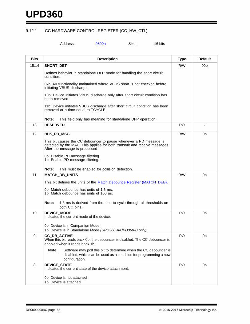
UPD360
9.12.1 CC HARDWARE CONTROL REGISTER (CC_HW_CTL)
Address: 0800h Size: 16 bits
Bits Description Type Default
15:14 SHORT_DET
Defines behavior in standalone DFP mode for handling the short circuit condition.
0xb: A0 functionality maintained where VBUS short is not checked before initiating VBUS discharge.
10b: Device initiates VBUS discharge only after short circuit condition has been removed.
11b: Device initiates VBUS discharge after short circuit condition has been removed or a time equal to TCYCLE.
Note: This field only has meaning for standalone DFP operation.
R/W 00b
13 RESERVED RO -
12 BLK_PD_MSG
This bit causes the CC debouncer to pause whenever a PD message is detected by the MAC. This applies for both transmit and receive messages. After the message is processed
0b: Disable PD message filtering.1b: Enable PD message filtering.
Note: This must be enabled for collision detection.
R/W 0b
11 MATCH_DB_UNITS
This bit defines the units of the Match Debounce Register (MATCH_DEB).
0b: Match debounce has units of 1.6 ms.1b: Match debounce has units of 100 us.
Note: 1.6 ms is derived from the time to cycle through all thresholds on both CC pins.
R/W 0b
10 DEVICE_MODEIndicates the current mode of the device.
0b: Device is in Companion Mode1b: Device is in Standalone Mode (UPD360-A/UPD360-B only)
RO 0b
9 CC_DB_ACTIVEWhen this bit reads back 0b, the debouncer is disabled. The CC debouncer is enabled when it reads back 1b.
Note: Software may poll this bit to determine when the CC debouncer isdisabled, which can be used as a condition for programming a newconfiguration.
RO 0b
8 DEVICE_STATEIndicates the current state of the device attachment.
0b: Device is not attached1b: Device is attached
RO 0b
DS00002084C-page 86 2016-2017 Microchip Technology Inc.
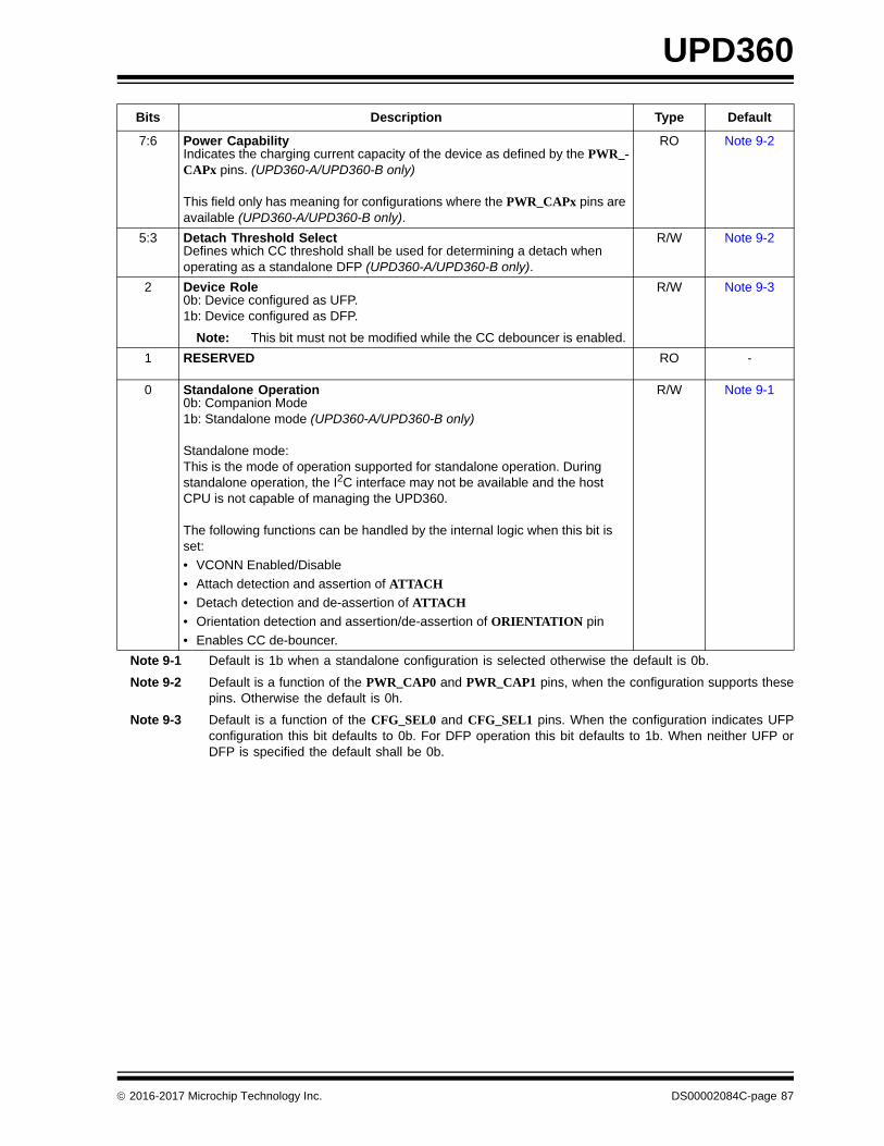
UPD360
Note 9-1 Default is 1b when a standalone configuration is selected otherwise the default is 0b.
Note 9-2 Default is a function of the PWR_CAP0 and PWR_CAP1 pins, when the configuration supports thesepins. Otherwise the default is 0h.
Note 9-3 Default is a function of the CFG_SEL0 and CFG_SEL1 pins. When the configuration indicates UFPconfiguration this bit defaults to 0b. For DFP operation this bit defaults to 1b. When neither UFP orDFP is specified the default shall be 0b.
7:6 Power CapabilityIndicates the charging current capacity of the device as defined by the PWR_-CAPx pins. (UPD360-A/UPD360-B only)
This field only has meaning for configurations where the PWR_CAPx pins are available (UPD360-A/UPD360-B only).
RO Note 9-2
5:3 Detach Threshold SelectDefines which CC threshold shall be used for determining a detach when operating as a standalone DFP (UPD360-A/UPD360-B only).
R/W Note 9-2
2 Device Role0b: Device configured as UFP.1b: Device configured as DFP.
Note: This bit must not be modified while the CC debouncer is enabled.
R/W Note 9-3
1 RESERVED RO -
0 Standalone Operation0b: Companion Mode1b: Standalone mode (UPD360-A/UPD360-B only)
Standalone mode:This is the mode of operation supported for standalone operation. During standalone operation, the I2C interface may not be available and the host CPU is not capable of managing the UPD360.
The following functions can be handled by the internal logic when this bit is set:
• VCONN Enabled/Disable
• Attach detection and assertion of ATTACH
• Detach detection and de-assertion of ATTACH
• Orientation detection and assertion/de-assertion of ORIENTATION pin
• Enables CC de-bouncer.
R/W Note 9-1
Bits Description Type Default
2016-2017 Microchip Technology Inc. DS00002084C-page 87

UPD360
9.12.2 CC INTERRUPT STATUS REGISTER (CC_INT_STS)
Address: 0803h Size: 16 bits
Bits Description Type Default
7 CC_MATCH_VLDAsserts after the CC debouncer is first enabled, via CC Comparator Control, and the first match becomes valid in CCx Match Registers (CCx_MATCH).
R/WC 0b
6 RP_CHGWhen operating as a standalone UFP, this interrupt indicates a change in the state of the RP value advertised by the DFP has been detected (UPD360-A/UPD360-B only).
Note: This bit is RO when the device is not configured as a standaloneUFP and will always read back 0b.
Note: The source of this input is a pulse and does not persist after beingcleared.
Note: The updated current advertisement is available via the DFP Cur-rent Advertisement field in the CC Control Register (CC_CTL).
R/WC 0b
5 DETACHIndicates a detach event has occurred when the device has been configured to support standalone mode per the Standalone Operation field in the CC Control Register (CC_CTL) (UPD360-A/UPD360-B only).
DFP Operation: CC pins are monitored for detecting a detach.UFP Operation: VBUS is monitored for detecting a detach.
Note: The source of this input is a pulse and does not persist after beingcleared.
R/WC 0b
4 ATTACHIndicates an attach event has occurred when the device has been configured to support standalone mode per the Standalone Operation field in the CC Control Register (CC_CTL) (UPD360-A/UPD360-B only).
DFP Operation: CC pins are monitored for an attach.UFP Operation: CC pins and VBUS are monitored for an attach.
Note: The source of this input is a pulse and does not persist after beingcleared.
R/WC 0b
3:2 RESERVED RO -
1 CC2_MATCH_CHGIndicates the a change occurred in the state of the respective CCx Change Status Registers (CCx_CHG_STS).
Note: The source of this input is a pulse and does not persist after beingcleared.
RO 0b
0 CC1_MATCH_CHGIndicates the a change occurred in the state of the respective CCx Change Status Registers (CCx_CHG_STS).
Note: The source of this input is a pulse and does not persist after beingcleared.
RO 0b
DS00002084C-page 88 2016-2017 Microchip Technology Inc.

UPD360
9.12.3 CCX CHANGE STATUS REGISTERS (CCX_CHG_STS)
9.12.4 CCX MATCH REGISTERS (CCX_MATCH)
Note 9-4 Defaults to FFh when the device is configured as a DFP and 00h when configured as a UFP, per theDevice Role field in the CC Control Register (CC_CTL).
Address: x=1: 0804hx=2: 0805h
Size: 8 bits
Bits Description Type Default
7:0 CCx Change StatusWhen set, each bit indicates that the respective bit in the CCx Match Regis-ters (CCx_MATCH) has changed.
A write of 1b clears the respective status bit.
R/WC 0h
Address: x=1: 0806hx=2: 0807h
Size: 8 bits
Bits Description Type Default
7:0 CCx Threshold Match (CCx_MATCH)When set, each bit indicates that the respective threshold programmed in the CC Threshold x Registers (CC_THRx) was matched. A match is determined when the measured voltage exceeds the programmed threshold.
These registers are updated after the Match Debounce Register (MATCH_DEB) while in the Unattached state. While in AttachWait state, these registers are updated after the PD Debounce Register (PD_DEB) if vOpen is seen for a time greater than in the PD Debounce Register (PD_DEB). While in Attached Source / Attached Sink states (e.g. detecting detach) the match registers are updated after the PD Debounce Register (PD_DEB).
Note: This register will always read the default value until the CC com-parator is enabled when not operating in standalone mode.
Note: The contents of this register are debounced per the settings in theCCx Debounce Clear Enable Registers (CCx_DBCLR_EN), other-wise the raw value shall be shown.
RO Note 9-4
2016-2017 Microchip Technology Inc. DS00002084C-page 89

UPD360
9.12.5 VBUS MATCH REGISTER (VBUS_MATCH)
Indicates which VBUS thresholds are matched on VBUS_DET pin. A match is determined when the measured voltageexceeds the programmed threshold.
9.12.6 VBUS CHANGE STATUS REGISTER (VBUS_CHG_STS)
Address: 0808h Size: 8 bits
Note: When not operating in standalone mode, this register will always read 0h until the VBUS comparator isenabled.
Note: The contents of this register shall be debounced per the settings in VBUS Debounce Clear Enable Register(VBUS_DBCLR_EN).
Bits Description Type Default
7:6 RESERVED RO -
5 VBUS Threshold 3 Match (VBUS3_THR_MATCH) RO 0b
4 VBUS Threshold 2 Match (VBUS2_THR_MATCH) RO 0b
3 VBUS Threshold 1 Match (VBUS1_THR_MATCH) RO 0b
2 VBUS Threshold 0 Match (VBUS0_THR_MATCH) RO 0b
1 RESERVED RO -
0 VBUS VSafe0v Match (VSAFE0V_THR_MATCH) RO 0b
Address: 0809h Size: 8 bits
Bits Description Type Default
7:0 VBUS Change Status (VBUS_CHG_STS)When set, each bit indicates that the respective bit in VBUS Match Register (VBUS_MATCH) has changed.
A write of 1b clears the respective status bit.
R/WC 0h
DS00002084C-page 90 2016-2017 Microchip Technology Inc.

UPD360
9.12.7 POWER INTERRUPT STATUS REGISTER (PWR_INT_STS)
Address: 080Ah Size: 8 bits
Bits Description Type Default
7 VBUS_MATCH_VLDAsserts after the VBUS debouncer is first enabled, via VBUS Comparator Control, and the first match becomes valid in VBUS Match Register (VBUS_-MATCH).
R/WC 0b
6 VCONN Discharge Error (VCONN_DISCH_ERR)When set this bit indicates that a VCONN discharge error has been detected. This bit is only available in standalone DFP mode and is otherwise reserved.
A discharge error is tracked when VCONN Discharge Control is set to 00b or 01b. A discharge error is asserted when VCONN fails to fall below VCONN Discharge Threshold (VCONN_DIS_THR) after a time greater than VCONN Discharge Time (VCONN_DIS_TIME) elapses.
R/WC 0b
5 CC2 Back-Drive ErrorWhen set, indicates that back-drive has been detected on the CC2 pin.
Note: The source of this input is a level and persists until the error condi-tion stops.
R/WC 0b
4 VBUS Discharge ErrorWhen set, indicates that the an interval greater than defined in the VBUS Off Register (VBUS_OFF) has elapsed while attempting to discharge VBUS.
Note: The source of this input is a pulse and does not persist after beingcleared.
R/WC 0b
3 VCONN2 FET PowerThe integrated VCONN2 FET is enabled and providing power.
This bit only has usefulness for standalone operation or where VCONN is explicitly enabled by the host.
Note: The source of this input is a level and persists until the VCONN isno longer present.
R/WC 0b
2 VCONN1 FET PowerThe integrated VCONN1 FET is enabled and providing power.
This bit only has usefulness for standalone operation or where VCONN is explicitly enabled by the host.
Note: The source of this input is a level and persists until the VCONN isno longer present.
R/WC 0b
1 CC1 Back-Drive ErrorWhen set indicates that back-drive has been detected on the CC1 pin.
Note: The source of this input is a level and persists until the error condi-tion stops.
R/WC 0b
0 VCONN Over-Current ErrorIndicates an over-current has been detected on the integrated VCONN FET.
Note: The source of this input is a level and persists until the error condi-tion stops.
R/WC 0b
2016-2017 Microchip Technology Inc. DS00002084C-page 91
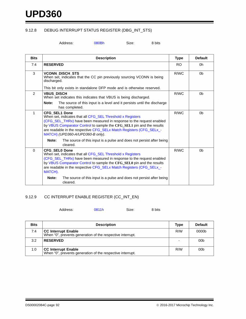
UPD360
9.12.8 DEBUG INTERRUPT STATUS REGISTER (DBG_INT_STS)
9.12.9 CC INTERRUPT ENABLE REGISTER (CC_INT_EN)
Address: 080Bh Size: 8 bits
Bits Description Type Default
7:4 RESERVED RO 0h
3 VCONN_DISCH_STSWhen set, indicates that the CC pin previously sourcing VCONN is being discharged.
This bit only exists in standalone DFP mode and is otherwise reserved.
R/WC 0b
2 VBUS_DISCHWhen set indicates this indicates that VBUS is being discharged.
Note: The source of this input is a level and it persists until the discharge has completed.
R/WC 0b
1 CFG_SEL1 DoneWhen set, indicates that all CFG_SEL Threshold x Registers (CFG_SEL_THRx) have been measured in response to the request enabled by VBUS Comparator Control to sample the CFG_SEL1 pin and the results are readable in the respective CFG_SELx Match Registers (CFG_SELx_-MATCH) (UPD360-A/UPD360-B only).
Note: The source of this input is a pulse and does not persist after beingcleared.
R/WC 0b
0 CFG_SEL0 DoneWhen set, indicates that all CFG_SEL Threshold x Registers (CFG_SEL_THRx) have been measured in response to the request enabled by VBUS Comparator Control to sample the CFG_SEL0 pin and the results are readable in the respective CFG_SELx Match Registers (CFG_SELx_-MATCH).
Note: The source of this input is a pulse and does not persist after beingcleared.
R/WC 0b
Address: 0811h Size: 8 bits
Bits Description Type Default
7:4 CC Interrupt EnableWhen “0”, prevents generation of the respective interrupt.
R/W 0000b
3:2 RESERVED - 00b
1:0 CC Interrupt EnableWhen “0”, prevents generation of the respective interrupt.
R/W 00b
DS00002084C-page 92 2016-2017 Microchip Technology Inc.
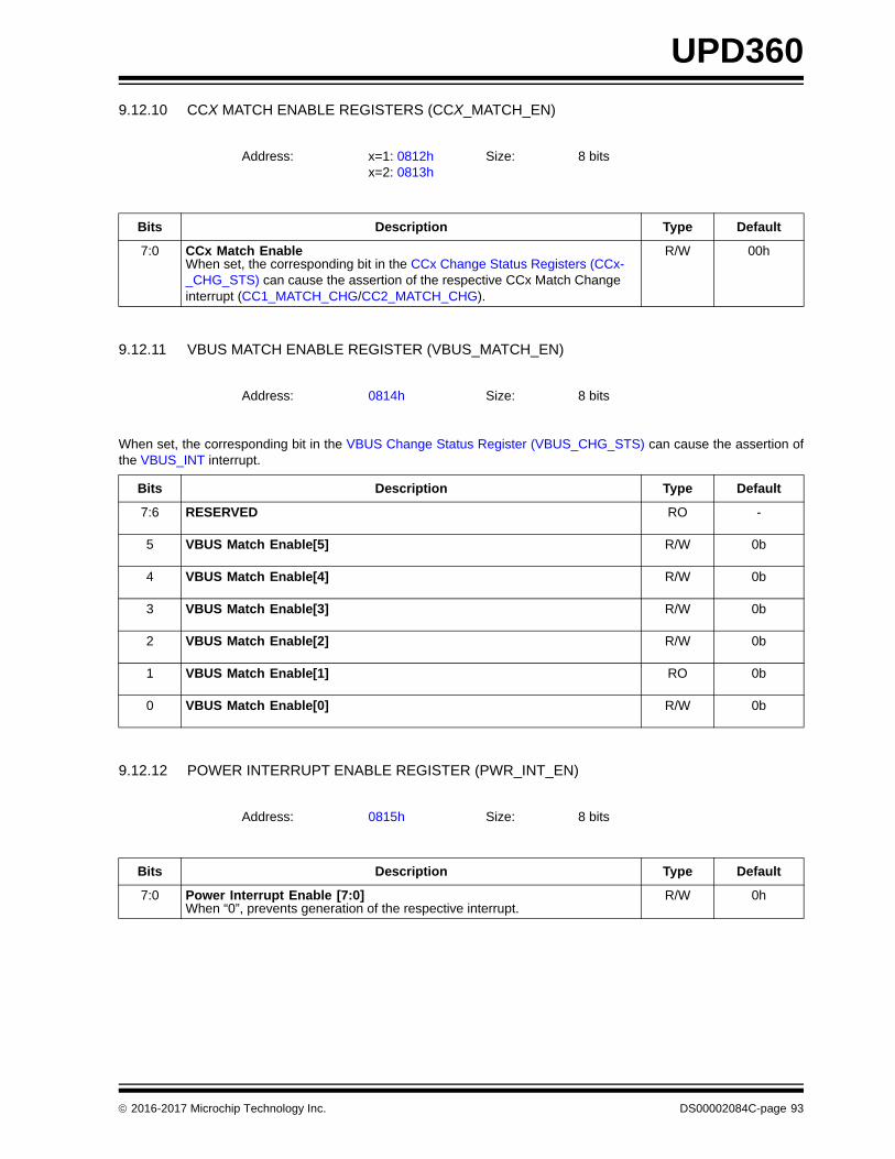
UPD360
9.12.10 CCX MATCH ENABLE REGISTERS (CCX_MATCH_EN)
9.12.11 VBUS MATCH ENABLE REGISTER (VBUS_MATCH_EN)
When set, the corresponding bit in the VBUS Change Status Register (VBUS_CHG_STS) can cause the assertion ofthe VBUS_INT interrupt.
9.12.12 POWER INTERRUPT ENABLE REGISTER (PWR_INT_EN)
Address: x=1: 0812hx=2: 0813h
Size: 8 bits
Bits Description Type Default
7:0 CCx Match EnableWhen set, the corresponding bit in the CCx Change Status Registers (CCx-_CHG_STS) can cause the assertion of the respective CCx Match Change interrupt (CC1_MATCH_CHG/CC2_MATCH_CHG).
R/W 00h
Address: 0814h Size: 8 bits
Bits Description Type Default
7:6 RESERVED RO -
5 VBUS Match Enable[5] R/W 0b
4 VBUS Match Enable[4] R/W 0b
3 VBUS Match Enable[3] R/W 0b
2 VBUS Match Enable[2] R/W 0b
1 VBUS Match Enable[1] RO 0b
0 VBUS Match Enable[0] R/W 0b
Address: 0815h Size: 8 bits
Bits Description Type Default
7:0 Power Interrupt Enable [7:0]When “0”, prevents generation of the respective interrupt.
R/W 0h
2016-2017 Microchip Technology Inc. DS00002084C-page 93
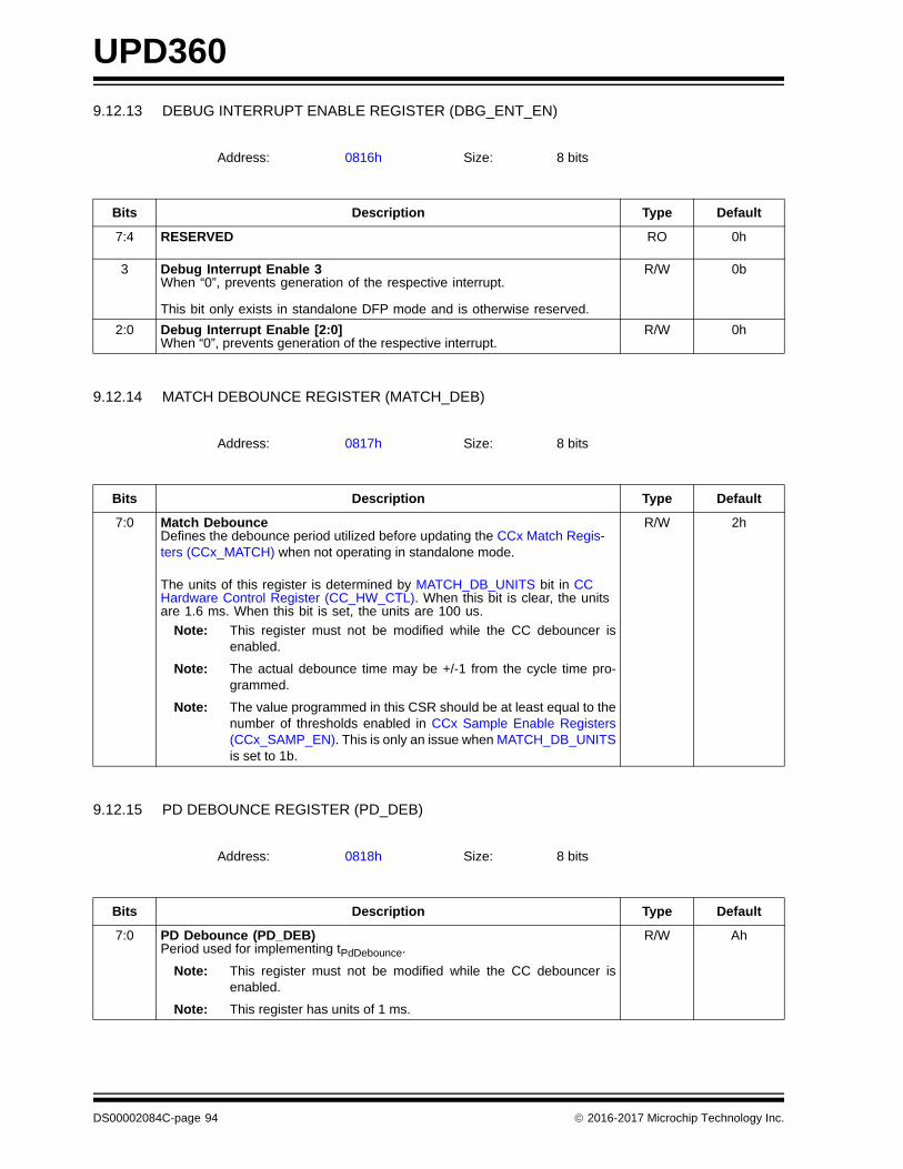
UPD360
9.12.13 DEBUG INTERRUPT ENABLE REGISTER (DBG_ENT_EN)
9.12.14 MATCH DEBOUNCE REGISTER (MATCH_DEB)
9.12.15 PD DEBOUNCE REGISTER (PD_DEB)
Address: 0816h Size: 8 bits
Bits Description Type Default
7:4 RESERVED RO 0h
3 Debug Interrupt Enable 3When “0”, prevents generation of the respective interrupt.
This bit only exists in standalone DFP mode and is otherwise reserved.
R/W 0b
2:0 Debug Interrupt Enable [2:0]When “0”, prevents generation of the respective interrupt.
R/W 0h
Address: 0817h Size: 8 bits
Bits Description Type Default
7:0 Match DebounceDefines the debounce period utilized before updating the CCx Match Regis-ters (CCx_MATCH) when not operating in standalone mode.
The units of this register is determined by MATCH_DB_UNITS bit in CC Hardware Control Register (CC_HW_CTL). When this bit is clear, the units are 1.6 ms. When this bit is set, the units are 100 us.
Note: This register must not be modified while the CC debouncer isenabled.
Note: The actual debounce time may be +/-1 from the cycle time pro-grammed.
Note: The value programmed in this CSR should be at least equal to thenumber of thresholds enabled in CCx Sample Enable Registers(CCx_SAMP_EN). This is only an issue when MATCH_DB_UNITSis set to 1b.
R/W 2h
Address: 0818h Size: 8 bits
Bits Description Type Default
7:0 PD Debounce (PD_DEB)Period used for implementing tPdDebounce.
Note: This register must not be modified while the CC debouncer isenabled.
Note: This register has units of 1 ms.
R/W Ah
DS00002084C-page 94 2016-2017 Microchip Technology Inc.

UPD360
9.12.16 VCONN OCS AND BACK-DRIVE DEBOUNCE REGISTER (VCONN_DEB)
9.12.17 CCX DEBOUNCE CLEAR ENABLE REGISTERS (CCX_DBCLR_EN)
Note 9-5 The default depends on the device’s configuration, as shown in table Table 9-10 which depends uponCFG_SEL0, PWR_CAP0, and PWR_CAP1 pins.
APPLICATION NOTE: Clearing a bit in CCx Debounce Clear Enable Registers (CCx_DBCLR_EN) shall cause therespective bit in CCx Match Registers (CCx_MATCH) to be immediately updated upon achange in state of the associated threshold. This causes a state change in CCx ChangeStatus Registers (CCx_CHG_STS) and assertion of CC_INT, if enabled. To prevent this CCxMatch Enable Registers (CCx_MATCH_EN) should be updated before the CCx DebounceClear Enable Registers (CCx_DBCLR_EN) by having the associated threshold cleared.
Address: 0819h Size: 8 bits
Bits Description Type Default
7:0 VCONN and Back-Drive Debounce (VCONN_DEB)Period used for implementing debounce of over-current detected on VCONN FET as well as back-drive detected on the CC pins.
Note: This register has units of 1 ms.
Note: This register should not be changed when VCONN OCS Enable isset.
R/W 2h
Address: x=1: 081Ahx=2: 081Bh
Size: 8 bits
Bits Description Type Default
7:0 CC Debounce Clear Enable (CC_DBCLR_DEB)When a bit is set, the respective threshold shall be included in the CC debouncer. Alternatively, when cleared the respective threshold shall no lon-ger be considered by the debouncer.
When CCx_DBCLR_EN bits are set on-the-fly, if a mismatch between the cur-rent raw match vector (for the new CCx_DBCLR_EN) and the previous raw match vector (for the old CCx_DBCLR_EN) exists, the DB will be reset.
Note: Clearing bits in this register at run time does not reset thedebouncer.
Note: The CC debouncer encompasses both CC1/CC2 pins. A detectedchange for a threshold on either pin results in the debouncer reset-ting.
Note: Even though this register may change on-the-fly, the internal logicwill enable the change only at the end of the scan cycle, which is afunction of whether the CC1/CC2 pins are actively sampled and theCCx Sample Enable Registers (CCx_SAMP_EN).
R/W Note 9-5
2016-2017 Microchip Technology Inc. DS00002084C-page 95
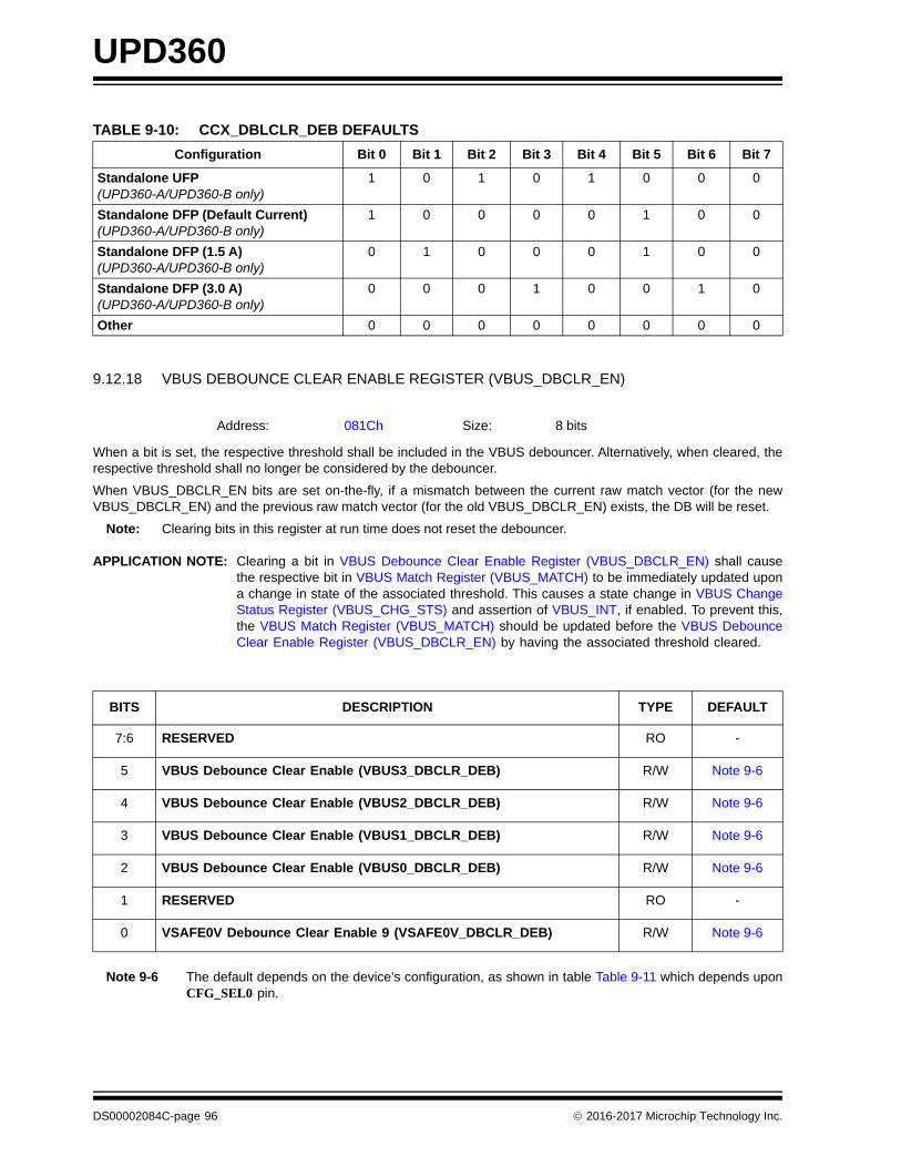
UPD360
9.12.18 VBUS DEBOUNCE CLEAR ENABLE REGISTER (VBUS_DBCLR_EN)
When a bit is set, the respective threshold shall be included in the VBUS debouncer. Alternatively, when cleared, therespective threshold shall no longer be considered by the debouncer.
When VBUS_DBCLR_EN bits are set on-the-fly, if a mismatch between the current raw match vector (for the newVBUS_DBCLR_EN) and the previous raw match vector (for the old VBUS_DBCLR_EN) exists, the DB will be reset.
Note: Clearing bits in this register at run time does not reset the debouncer.
APPLICATION NOTE: Clearing a bit in VBUS Debounce Clear Enable Register (VBUS_DBCLR_EN) shall causethe respective bit in VBUS Match Register (VBUS_MATCH) to be immediately updated upona change in state of the associated threshold. This causes a state change in VBUS ChangeStatus Register (VBUS_CHG_STS) and assertion of VBUS_INT, if enabled. To prevent this,the VBUS Match Register (VBUS_MATCH) should be updated before the VBUS DebounceClear Enable Register (VBUS_DBCLR_EN) by having the associated threshold cleared.
Note 9-6 The default depends on the device’s configuration, as shown in table Table 9-11 which depends uponCFG_SEL0 pin.
TABLE 9-10: CCX_DBLCLR_DEB DEFAULTS
Configuration Bit 0 Bit 1 Bit 2 Bit 3 Bit 4 Bit 5 Bit 6 Bit 7
Standalone UFP(UPD360-A/UPD360-B only)
1 0 1 0 1 0 0 0
Standalone DFP (Default Current)(UPD360-A/UPD360-B only)
1 0 0 0 0 1 0 0
Standalone DFP (1.5 A)(UPD360-A/UPD360-B only)
0 1 0 0 0 1 0 0
Standalone DFP (3.0 A)(UPD360-A/UPD360-B only)
0 0 0 1 0 0 1 0
Other 0 0 0 0 0 0 0 0
Address: 081Ch Size: 8 bits
BITS DESCRIPTION TYPE DEFAULT
7:6 RESERVED RO -
5 VBUS Debounce Clear Enable (VBUS3_DBCLR_DEB) R/W Note 9-6
4 VBUS Debounce Clear Enable (VBUS2_DBCLR_DEB) R/W Note 9-6
3 VBUS Debounce Clear Enable (VBUS1_DBCLR_DEB) R/W Note 9-6
2 VBUS Debounce Clear Enable (VBUS0_DBCLR_DEB) R/W Note 9-6
1 RESERVED RO -
0 VSAFE0V Debounce Clear Enable 9 (VSAFE0V_DBCLR_DEB) R/W Note 9-6
DS00002084C-page 96 2016-2017 Microchip Technology Inc.
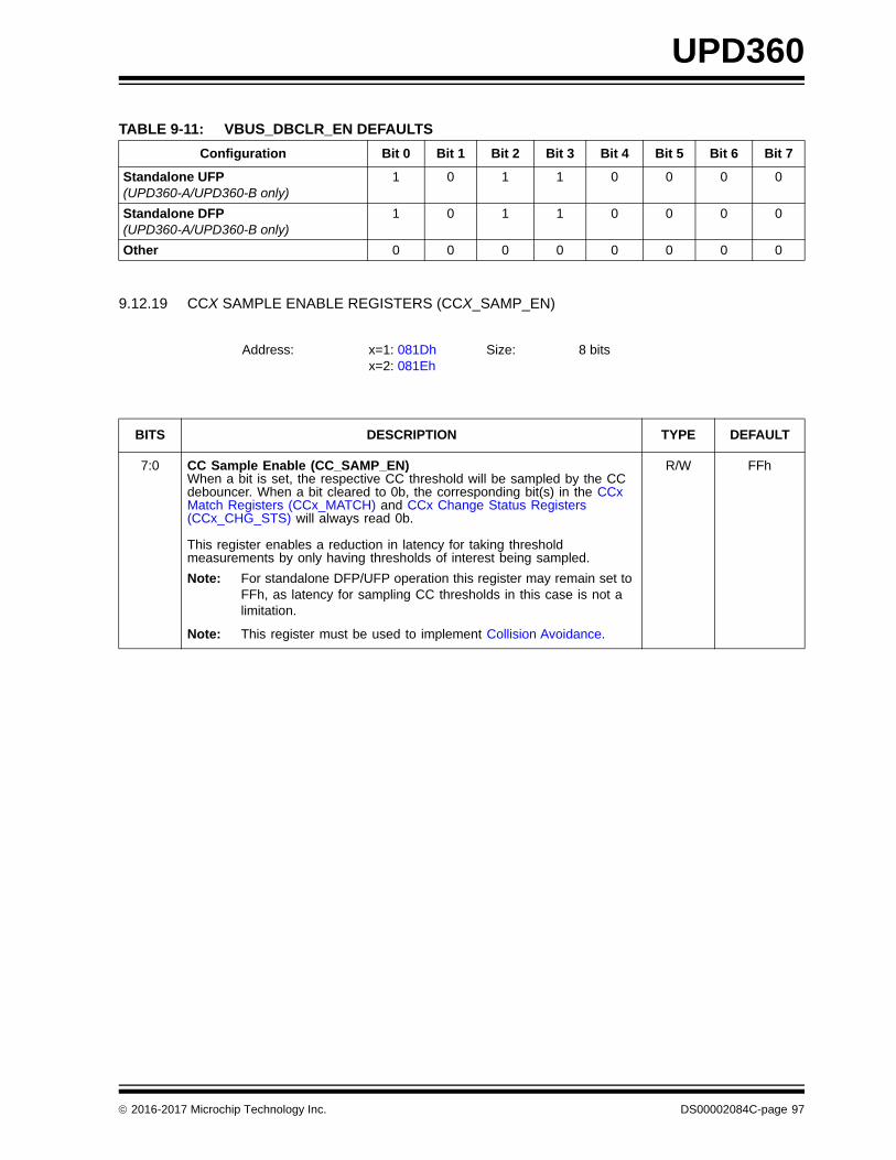
UPD360
9.12.19 CCX SAMPLE ENABLE REGISTERS (CCX_SAMP_EN)
TABLE 9-11: VBUS_DBCLR_EN DEFAULTS
Configuration Bit 0 Bit 1 Bit 2 Bit 3 Bit 4 Bit 5 Bit 6 Bit 7
Standalone UFP(UPD360-A/UPD360-B only)
1 0 1 1 0 0 0 0
Standalone DFP(UPD360-A/UPD360-B only)
1 0 1 1 0 0 0 0
Other 0 0 0 0 0 0 0 0
Address: x=1: 081Dhx=2: 081Eh
Size: 8 bits
BITS DESCRIPTION TYPE DEFAULT
7:0 CC Sample Enable (CC_SAMP_EN)When a bit is set, the respective CC threshold will be sampled by the CC debouncer. When a bit cleared to 0b, the corresponding bit(s) in the CCx Match Registers (CCx_MATCH) and CCx Change Status Registers (CCx_CHG_STS) will always read 0b.
This register enables a reduction in latency for taking threshold measurements by only having thresholds of interest being sampled.
Note: For standalone DFP/UFP operation this register may remain set to FFh, as latency for sampling CC thresholds in this case is not a limitation.
Note: This register must be used to implement Collision Avoidance.
R/W FFh
2016-2017 Microchip Technology Inc. DS00002084C-page 97
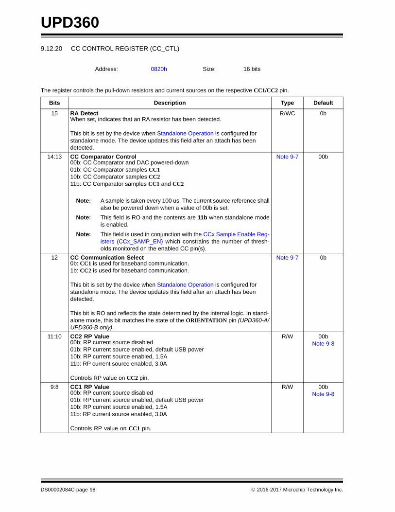
UPD360
9.12.20 CC CONTROL REGISTER (CC_CTL)
The register controls the pull-down resistors and current sources on the respective CC1/CC2 pin.
Address: 0820h Size: 16 bits
Bits Description Type Default
15 RA DetectWhen set, indicates that an RA resistor has been detected.
This bit is set by the device when Standalone Operation is configured for standalone mode. The device updates this field after an attach has been detected.
R/WC 0b
14:13 CC Comparator Control00b: CC Comparator and DAC powered-down01b: CC Comparator samples CC110b: CC Comparator samples CC211b: CC Comparator samples CC1 and CC2
Note: A sample is taken every 100 us. The current source reference shallalso be powered down when a value of 00b is set.
Note: This field is RO and the contents are 11b when standalone modeis enabled.
Note: This field is used in conjunction with the CCx Sample Enable Reg-isters (CCx_SAMP_EN) which constrains the number of thresh-olds monitored on the enabled CC pin(s).
Note 9-7 00b
12 CC Communication Select0b: CC1 is used for baseband communication.1b: CC2 is used for baseband communication.
This bit is set by the device when Standalone Operation is configured for standalone mode. The device updates this field after an attach has been detected.
This bit is RO and reflects the state determined by the internal logic. In stand-alone mode, this bit matches the state of the ORIENTATION pin (UPD360-A/UPD360-B only).
Note 9-7 0b
11:10 CC2 RP Value00b: RP current source disabled01b: RP current source enabled, default USB power10b: RP current source enabled, 1.5A11b: RP current source enabled, 3.0A
Controls RP value on CC2 pin.
R/W 00bNote 9-8
9:8 CC1 RP Value00b: RP current source disabled01b: RP current source enabled, default USB power10b: RP current source enabled, 1.5A11b: RP current source enabled, 3.0A
Controls RP value on CC1 pin.
R/W 00bNote 9-8
DS00002084C-page 98 2016-2017 Microchip Technology Inc.

UPD360
Note 9-7 This bit is RO when operating in standalone mode. Otherwise it is R/W.
Note 9-8 This field’s default is a function of the PWR_CAP0 and PWR_CAP1 pins when in standalone DFPmode (see Section 9.8.1, "Configuration Selection") (UPD360-A/UPD360-B only). Otherwise thedefault is 00b.
Note 9-9 For standalone DFP and standalone UFP, the value is 00b until the system reset completes.Afterwards, the default for standalone DFP is 11b and for standalone UFP is 01b.
9.12.21 CC THRESHOLD X REGISTERS (CC_THRX)
Note 9-10 The default varies as shown in Table 9-12.
7:6 DFP Current AdvertisementWhen Standalone Operation is configured for standalone mode and the device is configured as UFP, Device Role, this field indicates the DFP’s adver-tised current. Otherwise this field shall be read back 00b.
The device updates this field after an attach has been detected.
0xb: RP current advertises default USB current10b: RP current advertises 1.5A11b: RP current advertises 3.0A
RO 00b
5 RESERVED RO -
4:3 CC2 Pull-Down Value00b: Dead battery RD resistor selected01b: Trimmed RD resistor selected10b: Trimmed RA resistor selected.11b: Open Disconnect.
R/W Note 9-9
2 RESERVED RO -
1:0 CC1 Pull-Down Value00b: Dead battery RD resistor selected01b: Trimmed RD resistor selected10b: Trimmed RA resistor selected.11b: Open Disconnect.
R/W Note 9-9
Address: x=0: 0822hx=1: 0824hx=2: 0826hx=3: 0828hx=4: 082Ahx=5: 082Chx=6: 082Ehx=7: 0830h
Size: 16 bits
Bits Description Type Default
15:10 RESERVED RO -
9:0 CC Threshold X (CC_THRX)CC Threshold X register.
Note: The units of this register are ~2.44 mV from a 2.5V/1024.
Note: This register must not be modified while the CC debouncer isenabled.
R/W Note 9-10
Bits Description Type Default
2016-2017 Microchip Technology Inc. DS00002084C-page 99
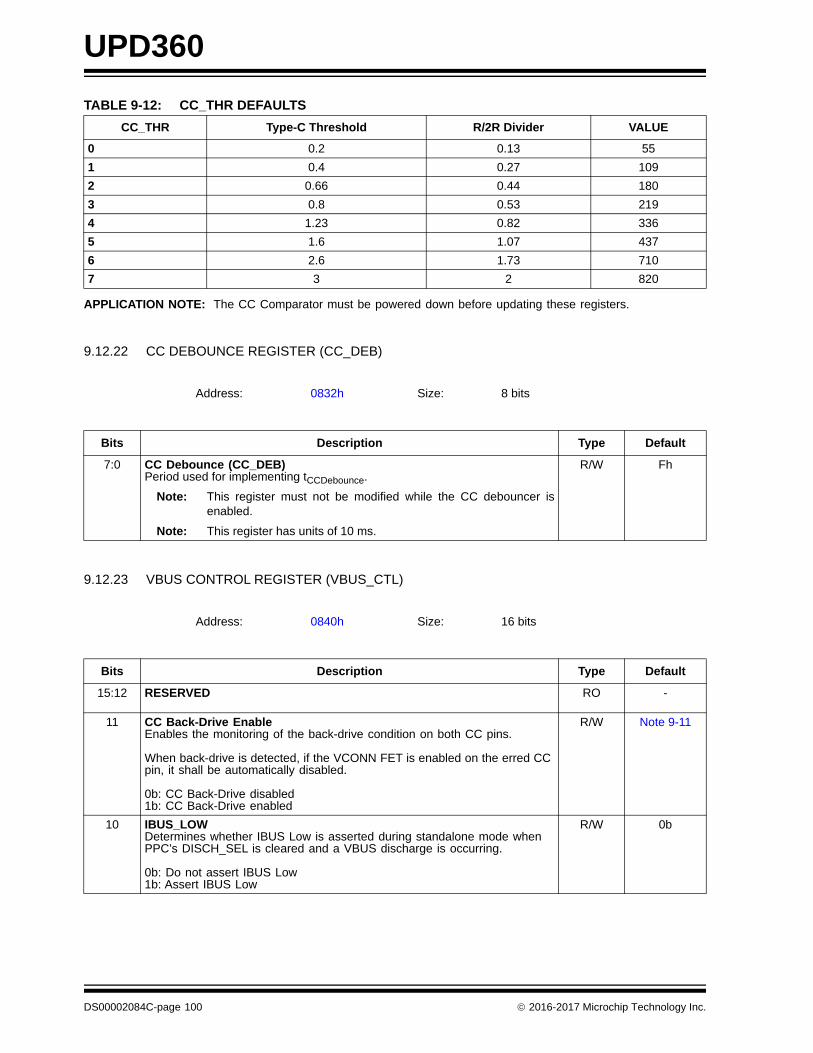
UPD360
APPLICATION NOTE: The CC Comparator must be powered down before updating these registers.
9.12.22 CC DEBOUNCE REGISTER (CC_DEB)
9.12.23 VBUS CONTROL REGISTER (VBUS_CTL)
TABLE 9-12: CC_THR DEFAULTS
CC_THR Type-C Threshold R/2R Divider VALUE
0 0.2 0.13 55
1 0.4 0.27 109
2 0.66 0.44 180
3 0.8 0.53 219
4 1.23 0.82 336
5 1.6 1.07 437
6 2.6 1.73 710
7 3 2 820
Address: 0832h Size: 8 bits
Bits Description Type Default
7:0 CC Debounce (CC_DEB)Period used for implementing tCCDebounce.
Note: This register must not be modified while the CC debouncer isenabled.
Note: This register has units of 10 ms.
R/W Fh
Address: 0840h Size: 16 bits
Bits Description Type Default
15:12 RESERVED RO -
11 CC Back-Drive EnableEnables the monitoring of the back-drive condition on both CC pins.
When back-drive is detected, if the VCONN FET is enabled on the erred CC pin, it shall be automatically disabled.
0b: CC Back-Drive disabled1b: CC Back-Drive enabled
R/W Note 9-11
10 IBUS_LOWDetermines whether IBUS Low is asserted during standalone mode when PPC’s DISCH_SEL is cleared and a VBUS discharge is occurring.
0b: Do not assert IBUS Low 1b: Assert IBUS Low
R/W 0b
DS00002084C-page 100 2016-2017 Microchip Technology Inc.

UPD360
9:8 OCS_MINDefines the minimum guaranteed assertion time for OCS_N when operating in standalone DFP mode (UPD360-A/UPD360-B only).
00b: 5 ms01b: 10 ms10b: 20 ms11b: 30 ms
R/W 00b
7 VBUS_DB_ACTIVEWhen this bit reads back 0b, the debouncer is disabled. The VBUS debouncer is enabled when it reads back 1b.
Note: Firmware polls this bit to determine when debouncer is disabledand a new configuration may be programmed.
RO 0b
6 VCONN OCS EnableEnables the monitoring of over current condition on the internal VCONN FETs.
0b: VCONN OCS monitor is disabled1b: VCONN OCS monitor is enabled
R/W Note 9-11
5:4 VCONN Discharge ControlThis field determines the VCONN discharge behavior. It only has meaning in DFP standalone mode and should not be used by firmware when operating in companion mode.
The discharge occurs on the CC pin that was supplying VCONN.
00b: Discharge VCONN until either the threshold defined by the VCONN Discharge Threshold Register (VCONN_DIS_THR) is reached or the time specified by the VCONN Discharge Time Register (VCONN_DIS_TIME) has expired.
01b: VCONN discharge is not supported.
10b: Discharge VCONN until threshold defined by VCONN Discharge Threshold Register (VCONN_DIS_THR) is reached.
11b: Discharge VCONN for the time specified by VCONN Discharge Time Register (VCONN_DIS_TIME).
Note: For options 0xb a VCONN discharge error is detected if the timer expires and VCONN has not discharged below VCONN Discharge Time Register (VCONN_DIS_TIME).
R/W 00b
3 VCONN2 ControlEnables the VCONN2 FET.
0b: VCONN2 FET is disabled1b: VCONN2 FET is enabled
This bit has no meaning when in standalone mode (see Standalone Opera-tion).
This bit automatically clears when a debounce VCONN OCS event occurs per the assertion of VCONN Discharge Error (VCONN_DISCH_ERR).
R/W 0b
Bits Description Type Default
2016-2017 Microchip Technology Inc. DS00002084C-page 101

UPD360
Note 9-11 This default value is 1 when operating in standalone DFP mode. Otherwise, the default value is 0.
Note 9-12 This field is RO and reads back 01b when operating in UFP standalone mode. In standalone modethis value does not indicate that VBUS is being actively measured. Whether or not VBUS is beingactively measured can be determined by reading VBUS_DB_ACTIVE.
9.12.24 VBUS THRESHOLD X REGISTERS (VBUS_THRX)
Note 9-13 The defaults are defined in Table 9-13.
2 VCONN1 ControlEnables the VCONN1 FET.
0b: VCONN1 FET is disabled1b: VCONN1 FET is enabled
This bit has no meaning when in standalone mode (see Standalone Opera-tion).
This bit automatically clears when a debounce VCONN OCS event occurs per the assertion of VCONN Discharge Error (VCONN_DISCH_ERR)
R/W 0b
1:0 VBUS Comparator Control00b: Comparator and DAC disabled01b: Sample VBUS10b: Sample CFG_SEL011b: Sample CFG_SEL1 (UPD360-A/UPD360-B only)
After the sample of CFG_SEL0 or CFG_SEL1 has completed, this register resets itself to 00b and disables the VBUS comparator.
Note: This field is forced to 01b by hardware when operating as a stand-alone UFP.
Note 9-12 00b
Address: x=0: 0842hx=1: 0844hx=2: 0846hx=3: 0848h
Size: 16 bits
Bits Description Type Default
15:10 RESERVED RO -
9:0 VBUS Threshold X (VBUS_THRX)VBUS Threshold X register.
The lower byte of the threshold must be written before the upper byte. The entire 10-bit threshold is updated when the second write occurs.
Note: The units of this register are ~2.44 mV from a 2.5V FS.
R/W Note 9-13
TABLE 9-13: VBUS_THR DEFAULTS
VBUS_THR VBUS Threshold 1R/9R Divider VALUE
0 3.67 0.36 148
1 5.5 0.54 222
2 5.5 0.54 222
3 5.5 0.54 222
Bits Description Type Default
DS00002084C-page 102 2016-2017 Microchip Technology Inc.
UPD360
9.12.25 VBUS DEBOUNCE REGISTER (VBUS_DEB)
This register has units of 1 ms.
9.12.26 VBUS OFF REGISTER (VBUS_OFF)
This register has units of 10 ms.
9.12.27 VBUS ERROR REGISTER (VBUS_ERR)
Address: 084Ah Size: 8 bits
Bits Description Type Default
7:0 VBUS Debounce (VBUS_DEB)Indicates debounce interval for the VBUS threshold comparators.
Note: This register must not be modified while the VBUS debouncer isenabled.
R/W 1h
Address: 084Bh Size: 8 bits
Bits Description Type Default
7:0 VBUS OffDefines timing after VBUS_DET discharges below VSafe0V.
R/W 10h
Address: 084Ch Size: 8 bits
Bits Description Type Default
7:3 RESERVED RO -
3 VCONN DischargeWhen set the VBUS Discharge error shall be enabled to place the device in the error state.
R/W 0b
2 VBUS DischargeWhen set, the VBUS Discharge error shall be enabled to place the device in the error state.
Note: This bit is not applicable when the PPC is selected for VBUS discharge.
R/W 0b
1 VCONN OCSWhen set, the CC OCS error shall be enabled to place the device in the error state.
R/W 0b
0 CC Back-driveWhen set, the CC back-drive error shall be enabled to place the device in the error state.
R/W 0b
2016-2017 Microchip Technology Inc. DS00002084C-page 103

UPD360
9.12.28 VBUS VSAFE0V THRESHOLD REGISTER (VSAFE0V_THR)
Note 9-14 The defaults are defined in Table 9-14.
APPLICATION NOTE: This register may be dynamically written to by software while the VBUS comparator isenabled, provided the rules for updating defined in the register description are followed.
9.12.29 CFG_SELX MATCH REGISTERS (CFG_SELX_MATCH)
Address: 084Eh Size: 16 bits
BITS DESCRIPTION TYPE DEFAULT
15:10 RESERVED RO -
9:0 VSAFE0V Threshold (VSAFE0V_THR)VSAFE0V Threshold register.
The lower byte of the threshold must be written before the upper byte. The entire 10-bit threshold is updated when the second write occurs.
Note: The units of this register are ~2.44 mV from a 2.5V FS.
R/W Note 9-14
TABLE 9-14: VSAFE0V_THR DEFAULTS
VSAFE0V_THR VBUS Threshold 1R/9R Divider VALUE
VSAFE0V_THR 0.8 0.08 32
Address: x=0: 0850hx=1: 0852h
Size: 16 bits
Bits Description Type Default
15:0 Configuration Select X Match (CFG_SELX_MATCH)Indicates which configuration select thresholds are matched on the CFG_SELx pin. A match is determined when the measured voltage exceeds the programmed threshold. See Section 9.8.1, "Configuration Selection," on page 81.
RO 0h
DS00002084C-page 104 2016-2017 Microchip Technology Inc.
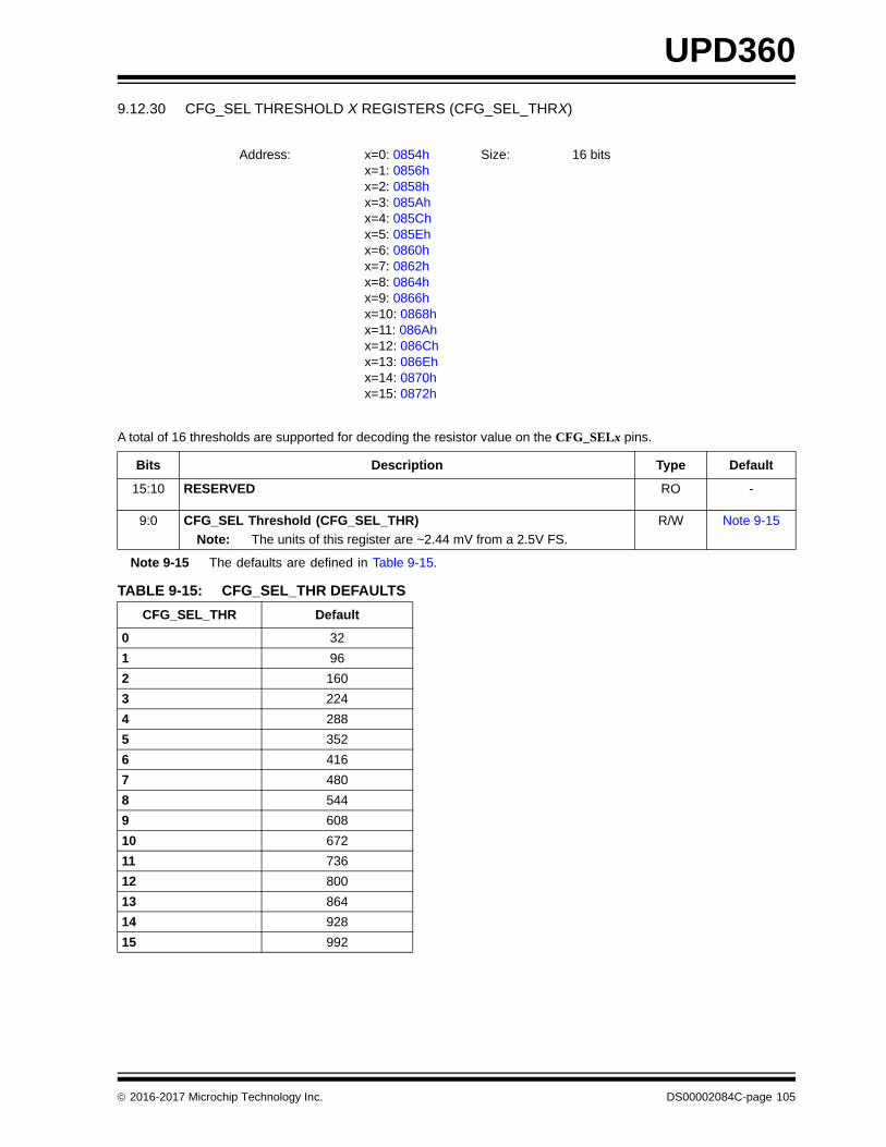
UPD360
9.12.30 CFG_SEL THRESHOLD X REGISTERS (CFG_SEL_THRX)
A total of 16 thresholds are supported for decoding the resistor value on the CFG_SELx pins.
Note 9-15 The defaults are defined in Table 9-15.
Address: x=0: 0854hx=1: 0856hx=2: 0858hx=3: 085Ahx=4: 085Chx=5: 085Ehx=6: 0860hx=7: 0862hx=8: 0864hx=9: 0866hx=10: 0868hx=11: 086Ahx=12: 086Chx=13: 086Ehx=14: 0870hx=15: 0872h
Size: 16 bits
Bits Description Type Default
15:10 RESERVED RO -
9:0 CFG_SEL Threshold (CFG_SEL_THR)
Note: The units of this register are ~2.44 mV from a 2.5V FS.
R/W Note 9-15
TABLE 9-15: CFG_SEL_THR DEFAULTS
CFG_SEL_THR Default
0 32
1 96
2 160
3 224
4 288
5 352
6 416
7 480
8 544
9 608
10 672
11 736
12 800
13 864
14 928
15 992
2016-2017 Microchip Technology Inc. DS00002084C-page 105
UPD360
9.12.31 CFG_SEL DEBUG REGISTER (CFG_SEL_DBG)
9.12.32 VCONN DISCHARGE THRESHOLD REGISTER (VCONN_DIS_THR)
Note 9-16 41 equates to 150mV after accounting for the R/2R divider.
9.12.33 VCONN DISCHARGE TIME REGISTER (VCONN_DIS_TIME)
Address: 0874h Size: 8 bits
Bits Description Type Default
7:4 CFG_SEL1_VALThis register stores a snapshot of the highest threshold matched when the device samples the CFG_SEL1 pin after a system level reset event (UPD360-A/UPD360-B only).
RO 0h
3:0 CFG_SEL0_VALThis register stores a snapshot of the highest threshold matched when the device samples the CFG_SEL0 pin after a system level reset event.
RO 0h
Address: 0886h Size: 16 bits
Bits Description Type Default
15:10 RESERVED RO -
9:0 VCONN Discharge Threshold (VCONN_DIS_THR)
This register defines the threshold used in standalone DFP mode for discharging VCONN.
Note: The units of this register are ~2.44 mV from a 2.5V/1024.
R/W 41hNote 9-16
Address: 0888h Size: 16 bits
Bits Description Type Default
7:0 VCONN Discharge Time (VCONN_DIS_TIME)
Defines the amount of time the CC pin supplying VCONN is discharged.
Note: The units of this register are 10 ms.
R/W 04h
DS00002084C-page 106 2016-2017 Microchip Technology Inc.
UPD360
10.0 BASEBAND CC INTERFACE (BCI)
The device integrates a Baseband CC Interface (BCI) to facilitate USB Power Delivery communication. This modulebridges between the PD MAC/BMC and the analog front end. Baseband communication is initiated by the PD MAC,which interfaces to the BCI. The BCI implements the digital functions required to control TX baseband components.
10.1 Baseband TX Data-flow
The key responsibility of the BCI is to generate the wave form required for baseband communication. To this end, theBMC has a group of eight registers that define the Lo-Hi and Hi-Lo transitions for the generated BMC signal.
When instructed to transition from Lo-Hi, the BCI steps through all BB TX Risex Registers (BB_RX_RISEx). Likewisewhen instructed to transition from Hi-Lo, the BCI steps through all BB TX Fallx Registers (BB_TX_FALLx). The BCIalways presents the value at BB_TX_RISE0 or BB_RX_FALL0 first.
APPLICATION NOTE: The user may replicate values if it is desired to use less than twelve unique values for thispurpose.
The following steps should be followed to program the BCI for data transmission:
1. Software programs the BB TX Risex Registers (BB_RX_RISEx) and BB TX Fallx Registers (BB_TX_FALLx) todefine the slew rate for rising and falling transitions.
2. Software enables the PD MAC.
3. The PD MAC initiates, either via firmware, or autonomously via a data transmission (GoodCRC). The PD MACinstructs the BCI to take the BB TX analog components out of power-down.
4. After a sufficient time elapses for the analog to power up, the PD MAC begins transmission to the BMC encoderwhich drives the analog components.
5. If the MAC requests a rising transition, the BCI steps through the BB TX Risex Registers (BB_RX_RISEx). Alter-natively, if the MAC requests a falling transition, the BCI steps through the BB TX Fallx Registers (BB_TX_-FALLx).
6. When the PD MAC indicates the transmission has completed, the BCI powers down the TX analog components.
10.2 Baseband RX Data-flow
Baseband RX data is received by the BCI from the RX analog front end where it is compared to a threshold programmedby software. The CC RX DAC Value defines the trip point used for reception of baseband data. The field shall be pro-grammed to be 175 mV below the RX Eye center, as defined in the PD Specification for the mode in which the deviceis operating (Sourcing Power, Sinking Power, Power Neutral).
In order to program the required trip point, the RX DAC Enable bit must be set and the CC RX DAC Value field in theCC RX DAC Control Register (CC_RX_DAC_CTL) must be programmed.
2016-2017 Microchip Technology Inc. DS00002084C-page 107
UPD360
10.3 Baseband CC Interface Registers
This section details the baseband CC interface registers. For an overview of the entire device register map, refer to Sec-tion 4.0, "Register Map," on page 19.
TABLE 10-1: BASEBAND CC INTERFACE REGISTER MAP
Address Register Name (Symbol)
2800h CC RX DAC Control Register (CC_RX_DAC_CTL)
2802h CC RX DAC Filter Register (CC_RX_DAC_FILT)
2803h Reserved for future expansion
2804h CC TX DAC Filter Register (CC_TX_DAC_FILT)
2805h – 280Fh Reserved for future expansion
2810h BB TX Risex Registers (BB_RX_RISEx) x=0
2812h BB TX Risex Registers (BB_RX_RISEx) x=1
2814h BB TX Risex Registers (BB_RX_RISEx) x=2
2816h BB TX Risex Registers (BB_RX_RISEx) x=3
2818h BB TX Risex Registers (BB_RX_RISEx) x=4
281Ah BB TX Risex Registers (BB_RX_RISEx) x=5
281Ch BB TX Risex Registers (BB_RX_RISEx) x=6
281Eh BB TX Risex Registers (BB_RX_RISEx) x=7
2820h BB TX Risex Registers (BB_RX_RISEx) x=8
2822h BB TX Risex Registers (BB_RX_RISEx) x=9
2824h BB TX Risex Registers (BB_RX_RISEx) x=10
2826h BB TX Risex Registers (BB_RX_RISEx) x=11
2828h – 282Fh Reserved for future expansion
2830h BB TX Fallx Registers (BB_TX_FALLx) x=0
2832h BB TX Fallx Registers (BB_TX_FALLx) x=1
2834h BB TX Fallx Registers (BB_TX_FALLx) x=2
2836h BB TX Fallx Registers (BB_TX_FALLx) x=3
2838h BB TX Fallx Registers (BB_TX_FALLx) x=4
283Ah BB TX Fallx Registers (BB_TX_FALLx) x=5
283Ch BB TX Fallx Registers (BB_TX_FALLx) x=6
283Eh BB TX Fallx Registers (BB_TX_FALLx) x=7
2840h BB TX Fallx Registers (BB_TX_FALLx) x=8
2842h BB TX Fallx Registers (BB_TX_FALLx) x=9
2844h BB TX Fallx Registers (BB_TX_FALLx) x=10
2846h BB TX Fallx Registers (BB_TX_FALLx) x=11
2848h – 2BFFh Reserved for future expansion
Note: RESERVED address space must not be written under any circumstances. Failure to heed this warn-ing may result in untoward operation and unexpected results.
DS00002084C-page 108 2016-2017 Microchip Technology Inc.
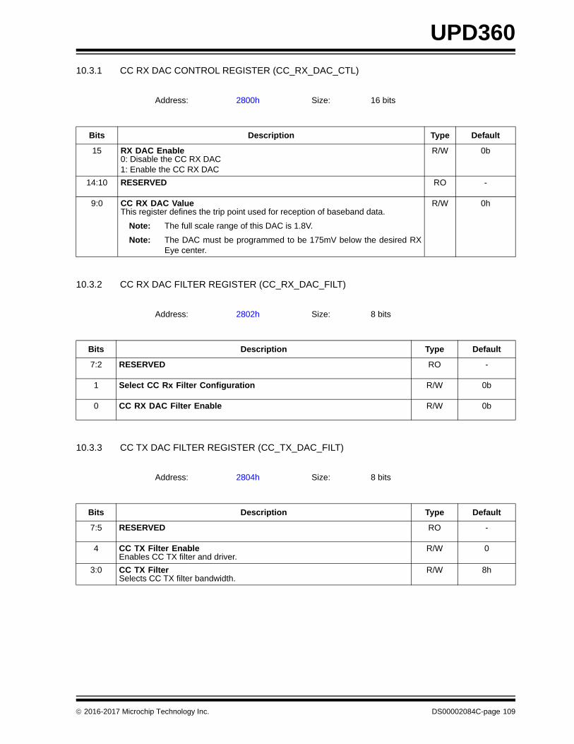
UPD360
10.3.1 CC RX DAC CONTROL REGISTER (CC_RX_DAC_CTL)
10.3.2 CC RX DAC FILTER REGISTER (CC_RX_DAC_FILT)
10.3.3 CC TX DAC FILTER REGISTER (CC_TX_DAC_FILT)
Address: 2800h Size: 16 bits
Bits Description Type Default
15 RX DAC Enable0: Disable the CC RX DAC1: Enable the CC RX DAC
R/W 0b
14:10 RESERVED RO -
9:0 CC RX DAC ValueThis register defines the trip point used for reception of baseband data.
Note: The full scale range of this DAC is 1.8V.
Note: The DAC must be programmed to be 175mV below the desired RXEye center.
R/W 0h
Address: 2802h Size: 8 bits
Bits Description Type Default
7:2 RESERVED RO -
1 Select CC Rx Filter Configuration R/W 0b
0 CC RX DAC Filter Enable R/W 0b
Address: 2804h Size: 8 bits
Bits Description Type Default
7:5 RESERVED RO -
4 CC TX Filter EnableEnables CC TX filter and driver.
R/W 0
3:0 CC TX FilterSelects CC TX filter bandwidth.
R/W 8h
2016-2017 Microchip Technology Inc. DS00002084C-page 109
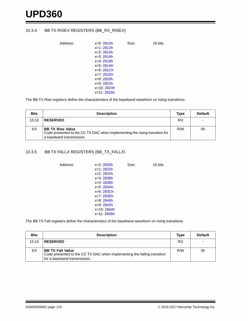
UPD360
10.3.4 BB TX RISEX REGISTERS (BB_RX_RISEX)
The BB TX Rise registers define the characteristics of the baseband waveform on rising transitions.
10.3.5 BB TX FALLX REGISTERS (BB_TX_FALLX)
The BB TX Fall registers define the characteristics of the baseband waveform on rising transitions.
Address: x=0: 2810hx=1: 2812hx=2: 2814hx=3: 2816hx=4: 2818hx=5: 281Ahx=6: 281Chx=7: 281Ehx=8: 2820hx=9: 2822hx=10: 2824hx=11: 2826h
Size: 16 bits
Bits Description Type Default
15:10 RESERVED RO -
9:0 BB TX Rise ValueCode presented to the CC TX DAC when implementing the rising transition for a baseband transmission.
R/W 0h
Address: x=0: 2830hx=1: 2832hx=2: 2834hx=3: 2836hx=4: 2838hx=5: 283Ahx=6: 283Chx=7: 283Ehx=8: 2840hx=9: 2842hx=10: 2844hx=11: 2846h
Size: 16 bits
Bits Description Type Default
15:10 RESERVED RO -
9:0 BB TX Fall ValueCode presented to the CC TX DAC when implementing the falling transition for a baseband transmission.
R/W 0h
DS00002084C-page 110 2016-2017 Microchip Technology Inc.

UPD360
11.0 POWER DELIVERY MAC
The PD MAC implements certain features of the protocol layer and physical layer of the Universal Serial Bus PowerDelivery Specification. On one end the PD MAC interfaces to the software implementing the bulk of protocol and higherlevel layers and on the other end it interfaces to a BMC encoder / decoder module.
In addition to the normal TX and RX functions, the PD MAC implements the test mode logic defined in the USB PDspecification (BIST).
The PD MAC supports the following features:
• Automatic TX Mode for packet framing and CRC32 insertion.
• Raw TX Mode for bit level packet control.
• Automatic GoodCRC response to received messages.
• Automatic BIST Error Count Message in BIST RX Mode.
• GoodCRCTimer implementation.
• Automatic retries with programmable retry count.
• Redundant receive packets automatically dropped in auto response mode.
• 74 byte TX queue.
• 128 byte RX queue.
• Programmable TX Bit-time. Allows for changing operating frequency.
• Programmable preamble length.
• BIST TX and RX logic.
• Programmable TX and RX queue modes - buffer mode and FIFO mode.
• CRC32 generator for TX.
• CRC32 calculator and comparator for RX.
11.1 PD MAC Transmitter
The PD MAC transmitter is comprised of three major blocks:
• TX Queue
• TX Control
• TX Comm
The TX Queue is where software loads the message to be transmitted.
The TX Control implements the necessary control logic. It is responsible for reading the data from the TX queue andbased on the data processing mode (automatic or raw), processing the data to make it suitable (nibbles with controlinformation) for use by the TX Comm. It is also responsible for generating packet framing and terminating the packet inautomatic mode, and generating messages for automatic response (GoodCRC and BIST Error Count). TX Control alsohandles the selection of the SOP type that is to be transmitted.
The TX Comm is comprised of a TX CRC generator, a 4b5b encoder, serializer, preamble generator, and TX bit timer.It takes the nibble data, computes and inserts the CRC, 5b encodes, and generates the baseband serial data. Preambleinsertion is also performed by this logic.
The following sub-sections describe the various blocks and sub-blocks in more detail. Some of the supported TX fea-tures are also described.
11.1.1 TX QUEUE
The TX Queue is where software loads the message to be transmitted. The following sub-sections describe the TXQueue in more detail.
11.1.1.1 TX Queue Modes of Operation
The TX Queue's write interface (MCU side) has two modes of operation: FIFO Mode and Buffer Mode.
11.1.1.1.1 FIFO Mode
This mode is enabled by setting the EN_FMQ bit in the TX Control Register A (TX_CTL_A). In this mode, software writesdata into the TX Queue like a FIFO. Software can use any offset address in the range of 1800h-1849h (although 1800hwould be logical to use). The FIFO is 74 entries deep. Data written to the FIFO cannot be read back by software.
2016-2017 Microchip Technology Inc. DS00002084C-page 111
UPD360
11.1.1.1.2 Buffer Mode
This mode is selected when the EN_FMQ bit in the TX Control Register A (TX_CTL_A) is cleared (default after POR).In this mode, software writes data into the TX Queue as if it were writing to registers at different addresses. The offsetaddress range is 1800h-1849h and the buffer has 74 locations.
Only byte access should be used while accessing the TX Queue in this mode. Note that buffer offset address 1800hcontains the least-significant-byte (LSB) (byte that goes out first). Buffer offset address 0x049 has the most-significant-byte (MSB) (byte that goes out last).
Software can arbitrarily write or read any location in the buffer. Only one packet can be queued into the TX Queue atone time. Queuing of multiple packets is not supported.
11.1.1.2 TX Queue Data and Processing Modes
The data placed in the TX Queue depends on the selected processing mode. Two modes are supported: “Auto ModeData Processing” (AMDP) and “Raw Mode Data Processing” (RMDP).
11.1.1.2.1 Auto Mode Data Processing (AMDP)
This mode is selected by clearing the EN_RMDP bit in the TX Control Register A (TX_CTL_A). In this mode, only themessage data (header and data objects) to be transmitted is queued in the TX Queue. Further, the data is queued asbytes. Since there is no framing information with the data, the TX Packet Length Register (TX_PKT_LEN) is used toprovide information about the length of message data. Hardware uses this information to determine when and where toappend the CRC. Packet framing (preamble, SOP, and EOP) is automatically inserted by the hardware.
11.1.1.2.2 Raw Mode Data Processing (RMDP)
This mode is selected by setting the EN_RMDP bit in the TX Control Register A (TX_CTL_A). In this mode, software isresponsible for constructing the entire packet including framing, except the preamble and CRC. Since framing involvesK-codes, the data placed in the queue is coded with control information. The data in each byte of the queue is treatedas a “nibble” of packet data that either needs to be 5b encoded by hardware or a K-codes that should be transmittedwithout any 5b encoding. There are also some special control bytes to control insertion of CRC and termination ofpacket.
When tx_queue_data[5] is “0” then tx_queue_data[3:0] is treated as 4b regular data. This 4b data goes through theCRC32 generator for CRC calculation and is encoded to 5b per Table 5-1 of USB PD Specification R1.0 (Table 11-1shows the 4b5b encoding).
When tx_queue_data[5] is “1” then tx_queue_data[4:0] is treated as 5b K-code (see Table 11-1). This data is eliminatedfrom the CRC calculation and does not go through any further encoding prior to transmission.
The tx_queue_data[7:0] values of 8'hFF and 8'hFE have special meaning. 8'hFF implies that the packet data is doneand hardware should now insert the calculated CRC32 (TX_INS_CRC). 8'hFE implies that the transmission should bestopped immediately (TX_STOP).
Note that in RMDP, software can compute its own CRC and place it in the Queue as encoded data. In this case, theTX_INS_CRC code would not be added to the Queue and instead software would proceed with adding the EOP andterminating the transfer with TX_STOP.
Table 11-1 shows how the byte wide queued data is interpreted or encoded by the transmission logic in raw mode.
DS00002084C-page 112 2016-2017 Microchip Technology Inc.

UPD360
Note that the tx_queue_data[4:0] is passed as-is when tx_queue_data[5] is set to 1. Thus, software can send reservedsymbols for error testing. The only caveat is that hardware cannot be used to generate and insert CRC. In this case,software should compute the necessary CRC32 and add it the data packet and skip the 0xFF code in the queue for CRCinsertion.
11.1.1.2.3 TX Queue Programming Sequence - AMDP
The following sequence should be used when programming a sequence in AMDP. This example assumes hardwareperforms packet framing and CRC insertion.
1. Make sure the GO bit in the TX Control Register B (TX_CTL_B) is cleared, i.e., hardware is done with previousTX request.
2. If using FIFO mode, clear the TX Queue WRI pointer by writing a “1” to the RST_TXQ_FIFO_WRI_PTR bit of theTX Control Register B (TX_CTL_B).
3. Write the two header bytes.
4. Write the payload data, if any.
5. Write the number of bytes to the TX Packet Length Register (TX_PKT_LEN).
6. Check to see if it is OK to transmit via the OK_TO_TX bit in the TX Control Register B (TX_CTL_B)).
7. If OK_TO_TX: set the GO bit in the TX Control Register B (TX_CTL_B) to start transmission.Else: repeat step 6. Note: If an RX is in progress, the current TX may need to be abandoned.
TABLE 11-1: RAW MODE DATA ENCODING
tx_queue_data[5:0] Encoded Symbol tx_queue_data[5:0] Encoded Symbol
6’h00 5’b11110 6’h08 5’b10010
6’h01 5’b01001 6’h09 5’b10011
6’h02 5’b10100 6’h0A 5’b10110
6’h03 5’b10101 6’h0B 5’b10111
6’h04 5’b01010 6’h0C 5’b11010
6’h05 5’b01011 6’h0D 5’b11011
6’h06 5’b01110 6’h0E 5’b11100
6’h07 5’b01111 6’h0F 5’b11101
tx_queue_data[5:0] K-Code Transmitted Data
6’b1_11000 Sync-1 5’b11000
6’b1_10001 Sync-2 5’b10001
6’b1_01101 EOP 5’b01101
6’b1_00111 RST1 5’b00111
6’b1_11001 RST2 5’b11001
tx_queue_data[5:0] Special Meaning
8’hFE TX_STOP
8’hFF TX_INS_CRC
2016-2017 Microchip Technology Inc. DS00002084C-page 113
UPD360
11.1.1.2.4 TX Queue Programming Sequence - RMDP
The following sequence should be used when programming a sequence in RMDP. This example assumes hardwareperforms CRC insertion.
1. Make sure the GO bit in the TX Control Register B (TX_CTL_B) is cleared, i.e., hardware is done with previousTX request.
2. If using FIFO mode, clear the TX Queue WRI pointer by writing a “1” to the RST_TXQ_FIFO_WRI_PTR bit of theTX Control Register B (TX_CTL_B).
3. Write the SOP K-Codes to the FIFO *Sync-1, Sync-1, Sync-1, Sync-2).
4. Write two header bytes, splitting each byte into nibbles.
5. Write the payload data, if any, splitting each byte into nibbles.
6. Write the value “0xFF” to insert the CRC.
7. Write the EOP K-Code (EOP).
8. Write the value “0xFE” to terminate the transmission. Failure to write this value will cause transmission to con-tinue indefinitely looping on the TX buffer.
9. Check to see if it is OK to transmit via the OK_TO_TX bit in the TX Control Register B (TX_CTL_B)).
10. If OK_TO_TX: set the GO bit in the TX Control Register B (TX_CTL_B) to start transmission.Else: repeat step 9. Note: If an RX is in progress, the current TX may need to be abandoned.
11.1.2 TX CONTROL
The TX Control implements the necessary control logic. It is responsible for reading the data from the TX queue andbased on the data processing mode (automatic or raw), processing the data to make it suitable (nibbles with controlinformation) for use by the TX Comm. It is also responsible for generating packet framing and terminating the packet inautomatic mode, and generating messages for automatic response (GoodCRC and BIST Error Count). TX Control alsohandles the selection of the SOP type that is to be transmitted.
11.1.2.1 Transmit Requests
There are four sources of transmit requests:
• GoodCRC Ack from the receiver for a soft-reset
• GoodCRC Ack from the receiver for a normal packet
• BIST error count message from the BIST receiver
• Transmit go from the software
11.1.2.2 Transmit Aborts
Once packet transmission is initiated, the device will power up the analog and then wait for the bus turn-around timersand power-up timers to expire. During this wait, the transmission can be aborted by software and will be aborted by thedevice, when a good packet (including soft-reset), a hard reset, or a cable reset (if enabled and the SOP type of thepending TX is SOP', SOP'', SOP'_Debug or SOP''_Debug) is received.
Once the bus turn-around time has expired (or if it was already expired) and the power up time is expired, the bus ischecked for idle. If the bus is idle, the transmission is started. If the bus is not idle, the transmission is discarded and,typically, an abort status set. This discard can be disabled with the WAIT4LINE_IDLE bit in the TX Control Register A(TX_CTL_A) for all packets and is also disabled for auto response triggered GoodCRC Acks for received soft-resets(unless the feature is disabled via the DIS_SPCL_SR_GCRC_ACK bit).
If the transmission is not discarded due to the bus being non-idle, the device waits for the bus to become idle and then,once again, waits the turn-around time. During the wait for bus idle, the transmission can be aborted by software andwill be aborted by the hardware if a good packet, a hard reset or a cable reset (if enabled and the SOP type of the pend-ing TX is SOP', SOP'', SOP'_Debug or SOP''_Debug) is received.
Software issued hard and cable resets are not aborted due to received good packets, hard resets or cable resets.
Note: The value of the TX Packet Length Register (TX_PKT_LEN) is ignored for this mode since hardware knowswhen to terminate the packet based on detection of TX_STOP control code.
DS00002084C-page 114 2016-2017 Microchip Technology Inc.

UPD360
Note that for a received good packet to abort a pending transmission, the SOP type of the received packet must matchthe SOP type of the pending transmission, or the SOP type of the received packet must be SOP with the SOP type ofthe pending transmission being non-SOP (the latter can be disabled via the DIS_SOP_ABRTS_NON_SOP bit in the TXControl Register A (TX_CTL_A)) and, for messages other than Soft-Reset, the received message ID must indicate anon-duplicated packet (Soft-Resets are never considered duplicates). Ping and GoodCRC messages do not cause atransmission to abort.
Separate TX interrupt abort bits and separate abort status registers are provided for software issued and auto-responsepackets.
11.1.2.3 Transmit Retries
Transmitted packets are retried under two scenarios: bus idle violations, and GoodCRC response timeout.
If the transmission is discarded due to the bus being non-idle, the option exists to retry instead of treating it as an abort.In order for this to occur, the packet must have been initiated by software, not be a hard or cable reset, auto responsemode must be enabled, the retry count must be non-zero, and the RETRY_ON_LINE_BUSY bit in the TX Control Reg-ister A (TX_CTL_A) must be set. If after the specified number of retries, the transmission failed due to bus busy, theTX_FAILED status is set (not TX_ABORTED). Hard and Cable resets are not retried.
Following the transmission of a software initiated frame (other than Hard and Cable resets), the device will start a timerand wait for a GoodCRC response to be indicated by the receiver. This assumes retries and / or the wait for GoodCRCare enabled.
If a GoodCRC is received with the correct SOP type and message ID, then the wait is finished and the transmission isdone. If a GoodCRC is received with the wrong SOP type or message ID, it is ignored by the transmitter (the transmitteris not even notified) and silently dropped by the receiver.
If the wait for CRC timer expires and the remaining retry count is non-zero, the original packet is re-transmitted. If theremaining retry count is zero, then the packet is not retried and a failed status is indicated.
The wait for GoodCRC will be aborted if any of the following are received:
• A hard reset
• A cable reset (if cable reset reception is enabled and the SOP type of the pending TX is SOP', SOP'', SOP'_De-bug or SOP''_Debug)
• A soft-reset (if the SOP type of the RX is the same as that of the pending TX or the SOP type of the RX is SOP with the SOP type of the pending transmission being non-SOP)
• A good packet other than a GoodCRC or Ping (if the SOP type of the RX is the same as that of the pending TX or the SOP type of the RX is SOP with the SOP type of the pending transmission being non-SOP (the latter can be disabled via the DIS_SOP_ABRTS_NON_SOP bit in the TX Control Register A (TX_CTL_A)) and the package is not a duplicate message)
The latter two causes are considered to be protocol errors.
The wait for GoodCRC can also be aborted by software. An aborted wait for GoodCRC is not retried.
11.1.2.4 Transmitter Disable
In order to avoid a race condition where the software is currently issuing a transmit and the hardware is receiving apacket, the EN_FWTX bit in the TX Parameters Register A (TX_PARAM_A) is automatically cleared if a hard reset to acable reset (if enabled - no SOP type checking is done since a transmission may not be pending) has been received(based on the RX_CABLE_RST and RX_HARD_RST bits in the RX Interrupt Status Register (RX_IRQ_STAT)) or ifthere is any data in the RX FIFO. Using the interrupt and FIFO status (level sensitive) instead of the even occurrence(edge) avoids another race condition where the software has set the EN_FWTX bit just following the event.
11.1.3 TX COMM
The TX Comm is responsible for taking the coded nibbles from TX Control, encoding it if necessary, and serializing tomake it ready for transmission. It is responsible for preamble insertion, CRC calculation, and CRC insertion. It also pro-vides the TX clock signal for the BMC encoder.
11.1.3.1 Preamble Insertion
The device automatically adds the alternating “0” and “1” preamble to the transmitted packet. When the transmission ofthe preamble is completed, data from TX Queue is processed under direction of the TX Control.
2016-2017 Microchip Technology Inc. DS00002084C-page 115

UPD360
The number of preamble bits sent is programmable by the value of the PREAMBLE_LEN bit in the TX Parameters Reg-ister B (TX_PARAM_B).
11.1.3.2 TX CRC32
The transmit CRC is reset at the start of transmission (setting of the GO bit in the TX Control Register B (TX_CTL_B)or by triggering of automatic response by hardware).
The coded nibble data is streamed into the TX CRC32 one nibble at a time for CRC calculation. Only valid D-Code datais used in CRC calculation. All framing data (invalid D-Code) is excluded from CRC calculation.
11.1.3.3 TX Bit Timing
The baseband transmit signal bit time is controlled by the value in the TX Bit-Time Count Register (TX_BITTIME_CNT).This value determines the transmit data rate.
The count value is based on clock frequency and is given by:((Clock Freq KHz / Bit Rate Kbps) - 1)
For example:
Clock Frequency = 48000KHz (48MHz)Nominal Bit Rate = 300 Kbpsbit_time_cnt = (48000 / 300) - 1 = 159
11.1.4 AUTOMATIC RESPONSE MODE
The device supports an Automatic Response Mode (not to be confused with automatic-data processing mode). In thismode, the device will automatically send a GoodCRC message upon successful packet reception, or a BIST Error Countmessage upon reception of a BIST PRBS frame. This mode can be enabled by setting the EN_AUTO_RSP_MODE bitin the TX Control Register A (TX_CTL_A).
During normal auto-response, if the bus if found to be busy when the device attempts to send the auto-response (shouldnot happen, except if there is noise) it will abort the transmission and the AUTO_RSP_ABORTED bit in the TX InterruptStatus Register (TX_IRQ_STAT) will be set. This behavior can be altered by setting the WAIT4LINE_IDLE bit in the TXControl Register A (TX_CTL_A). Setting this bit will force the device to wait until the bus becomes idle (refer to theWAIT4LINE_IDLE bit description for additional information). GoodCRCs and BIST Error Count messages are not retriedeven if RETRY_ON_LINE_BUSY in TX_CTL_A is set.
In USB Power Delivery Revision 1.0, Soft Reset had a one-strike rule and failure of Soft Reset led to Hard Reset, leadingto the link being brought down, therefore the transmission of GoodCRC ACK in response to reception of Soft Reset ishandled a little differently. If hardware finds that the line is busy when it attempts to send the GoodCRC ACK it will waituntil the line becomes idle and then re-try the transmission. This process will happen indefinitely. This behavior is sameas what happens to normal GoodCRC ACK when WAIT4LINE_IDLE bit is set. GoodCRCs are not retried even if theRETRY_ON_LINE_BUSY bit in the TX Control Register A (TX_CTL_A) is set. For USB Power Delivery Revision 3.0,Soft Resets are normally retried, therefore this function should be disabled via the DIS_SPCL_SR_GCRC_ACK bit.
The SOP type that is used for the automatically sent GoodCRC packet is the SOP type of the received packet (parsedby the receiver). The SOP type that is used for the BIST Error Count message, is selected via the TX_SOP_SELECTbit in the TX Parameters Register A (TX_PARAM_A).
For both GoodCRC and BIST Error Count messages, bit 8 in the packet header is taken from either the PORT_POW-ER_ROLE (for SOPs) or the CABLE_PLUG (for SOP', SOP'' and _debugs) bits within the TX Parameters Register C(TX_PARAM_C), depending on the SOP type that was received. Bit 5 in the packet header is taken from either thePORT_DATA_ROLE bit (for SOPs) or set to zero (for SOP', SOP'' and _debugs), depending on the SOP type that wasreceived.
In order to avoid missing an auto response GoodCRC request, a flag is used. The flag is set with a request pulse fromthe receiver and is cleared when the response is sent or aborted. Along with the request flag being set, the SOP typeand message ID of the request as well as the Soft Reset response indication are saved. In the event that there was a
Note: Setting the PREAMBLE_LEN field to an odd value will cause violation of the USB PD Specification whichstates “The preamble shall start with a “0” and shall end with a “1”.” An odd value will cause preamble tostart with a value of “0” but it will also end in a value of “0.” Setting this field to an odd value may or maynot lead to functional issues. Therefore, this field should be set to an even value to remain USB PD Spec-ification compliant.
Note: The CRC32 algorithm is described in the USB PD Specification.
DS00002084C-page 116 2016-2017 Microchip Technology Inc.
UPD360
pending auto response GoodCRC request and another packet was received resulting in another auto response Good-CRC request, the second request will replace the first request, unless the first request had a SOP type of SOP and thesecond request had a SOP type of SOP'_Debug or SOP'’_Debug. This replacement occurs regardless of the setting ofthe DIS_SOP_ABRTS_NON_SOP bit in the TX Control Register A (TX_CTL_A). Even if a received packet does notabort a pending auto response, the pending auto response may get replaced by a new auto response.
11.1.5 AUTOMATIC RETRY MODE
The device also supports an Automatic Retry Mode. In this mode, when a GoodCRC message is not received in theappropriate time (i.e., before CRCReceiveTimer expires) the current message is retried.
Hardware will retry the message until the retry value specified in the N_RETRY_CNT field in the TX Parameters Reg-ister C (TX_PARAM_C) is satisfied. If the N_RETRY_CNT is set to zero, Automatic Retry Mode is disabled.
The number of retries used by the device to complete the transaction are tracked and made available to software viathe N_HW_RETRIES field in the TX Status Register (TX_STAT).
An N_RETRY_CNT value of zero implies the message is attempted only once, i.e., hardware will not retry it. N_RE-TRY_CNT specifies the number of retries so the number of attempts is (N_RETRY_CNT + 1). Stated another way, ifyou want hardware to make “N” attempts to send a message then the N_RETRY_CNT field must be set to “N-1.”
Reception of Hard Reset or Cable reset (when enabled and the SOP type of the pending TX is SOP', SOP'', SOP'_De-bug or SOP''_Debug) from port partner, messages other than GoodCRC or Ping message (if the SOP types of the RXand TX match or if the SOP type of the RX is SOP with the SOP type of TX being non-SOP (the latter can be disabledvia the DIS_SOP_ABRTS_NON_SOP bit in the TX Control Register A (TX_CTL_A)) and the packet was not a dupli-cate), or issuance of abort by software will terminate any pending auto retries.
Detection of bus collision will cause the device to abort the current transfer including any pending auto retries unlessthe RETRY_ON_LINE_BUSY bit in the TX Control Register A (TX_CTL_A) is set.
Note that disabling of automatic-retry by setting N_RETRY_CNT to zero will also disable the device’s ability to wait fora GoodCRC message before a successful message transmission is indicated. This applies, for example, to the casewhen Soft Reset is transmitted. To circumvent this limitation, a EXPECT_GOODCRC bit in the TX Parameters RegisterA (TX_PARAM_A) is available. Setting this bit will cause the device to wait for a GoodCRC in response to a TX mes-sage, even when the N_RETRY_CNT field is set to zero.
The expected message ID within the GoodCRC message is set by software via the MSG_ID field in the TX ParametersRegister A (TX_PARAM_A). This is compared to the message ID within the received GoodCRC message.
The expected SOP type within the GoodCRC message is set by software via the TX_SOP_SELECT field in the TXParameters Register A (TX_PARAM_A). This is compared to the SOP type received in the GoodCRC message. In orderfor the GoodCRC message to be received, it is assumed that the SOP type has been enabled via the RX_SOP_EN-ABLE field in the RX Control Register B (RX_CTL_B).
11.1.6 IFG TIMER
The TX turn-around timer is used to insure that a minimum bus idle time is guaranteed between packet reception andpacket transmission, i.e., sending of GoodCRC message upon successful packet reception.
The value of this timer is programmable via the TX Turnaround Time Register (TX_TA_TIME). The value is specified inuSec. This timer uses the free-running 1us pulse so the value of this register should be 1 more than desired to ensurethe minimum time.
11.1.7 CRC RECEIVE TIMER
This timer is enabled when the device is expected to wait for a GoodCRC ACK (i.e., automatic-retry mode is enabledby non-zero value in the N_RETRY_CNT field of the TX Parameters Register C (TX_PARAM_C) or if zero, EXPECT_-GOODCRC bit in the TX Parameters Register A (TX_PARAM_A) is set) at the time transmission is requested. This timercan also be enabled for software usage via the EN_CRC_RCV_TMR bit in the RX Control Register A (RX_CTL_A).
If enabled, the timer starts whenever a TX packet transmission stops.
If software aborts a TX packet in between transmission with auto-retry mode enabled, this timer will not be triggered andwill be disabled. If software aborts a TX packet with auto-retry disabled, then it should also disable the timer by clearingthe EN_CRC_RCV_TMR bit in the RX Control Register A (RX_CTL_A).
Note: Setting N_RETRY_CNT to zero after the GO bit has been set will have no effect for the current transfer.
2016-2017 Microchip Technology Inc. DS00002084C-page 117
UPD360
The timeout value for CRCReceiveTimer is programmable via the TRECEIVE field in the RX tReceive Time Register(RX_TRECEIVE_TIME) in multiples of 10 uSec.
This timer can be used by software as the BISTReceiveErrorTimer in the BIST TX mode (the device does not automat-ically time BISTReceiveError) and as the CRCReceiveTimer when not using automatic retry or wait for GoodCRCmodes.
11.1.8 ABORTING A TX IN PROCESS
Software can abort a transmission that has already started by issuing an abort via the ABORT bit in the TX Control Reg-ister B (TX_CTL_B). The packet will be aborted as follows based on current phase of transmission:
• If packet transmission had not yet started because the device was waiting for the turn-around timer to expire or line to become idle, transmission will be aborted immediately.
• If the current phase is Preamble, the device will complete transfer of the current bit, append EOP, and turn the transmitter off.
• If the current phase is SOP, Data, or CRC, the device will complete transfer of the current nibble, append EOP, and turn the transmitter off.
A Hard Reset should follow this operation, which is the software's responsibility.
11.2 PD MAC Receiver
The PD MAC receiver is comprised of three major blocks:
• RX Queue
• RX Control
• RX Comm
The RX Queue is where software reads the received messages.
The RX Control implements the necessary control logic. It is responsible for validating the received packet, updating theRX Queue status, and triggering automatic responses, if required.
The RX Comm is comprised of the Clock and Data Recovery (CDR), RX DES (de-serializer) (serial-to-parallel converter,4b5b decoder, and framing detector), RX CRC32 (CRC calculator, receive timer), and other logic to detect valid packetreception.
The following sub-sections describe the various blocks and sub-blocks in more detail.
11.2.1 RX QUEUE
The decoded RX data (header, data objects, and CRC) is saved into an integrated 128 byte RX FIFO. The RX FIFO thatis capable of storing multiple packets and provides read and write pointers.
Two bytes are added to the beginning of each packet. Byte 0 holds the packet status (SOP type and the legacy “buffer”valid bit) and byte 1 holds the packet length. An option exists to swap these values (length in byte 0, status in byte 1)and add one to the packet length (to account for the status byte). This option is used for an SMBus like block read wherethe first byte read indicates the length of the transfer and the remaining bytes (the status and the packet) follow. Notethat the packet includes the 4 byte CRC, which is included in the length.
The following sub-sections present details of how the write and read interfaces to the FIFO appear.
DS00002084C-page 118 2016-2017 Microchip Technology Inc.
UPD360
11.2.1.1 RX FIFO Write Interface
Figure 11-1 shows how the write interface (from receive hardware's perspective) appears at various points of reception.
Each RX Packet is comprised of two bytes of control information and the received packet data. The Status byte indicateswhether the data is valid and the SOP type that was received. A value of 0x00 in the status byte implies that the data isnot valid (including the NBytes field).When bit 0 of the status byte is 1'b1, the Nbytes field indicates the length of thepacket and bits 6:4 of the status byte indicates the SOP type that was received. An empty FIFO always returns a valueof 0x00. However, the status byte should not be polled, but rather the RX_FIFO_NOT_EMPTY bit in the RX InterruptStatus Register (RX_IRQ_STAT) should be used. The valid bit is retained for legacy compatibility. When software readsthe packet data from the FIFO, it should only read number of bytes indicated by Nbytes (in addition to the Nbytes andStatus entries). Note that the byte count indicated by NBytes includes the CRC32 data.
When SMBus mode is enabled (via the EN_SMBUS_MODE bit in the RX Control Register A (RX_CTL_A)), the Statusand Nbytes fields are swapped and Nbytes is incremented by 1 to include the status byte. The swapping makes the(not-recommended) polling of the Status byte impossible for this mode. When software reads the packet data from theFIFO, it should only read number of bytes indicated by NBytes (in addition to the Nbytes entry). Figure 11-2 details theformat while in SMBus mode.
FIGURE 11-1: WRITE INTERFACE VIEW OF RX FIFO
FIGURE 11-2: RX FIFO SMBUS MODE
CRC (4)byte m
byte 0MessageHeader
CRC (4)byte n
byte 0MessageHeader
Ram Address
Nbytes*Status*
CRC (4)byte n
byte 0MessageHeader
1900h
197Fh
<- Write Head Pointer
Pa
cke
t 0
*assuming SMBus mode = 0
Free Space
Free Space
<- Write Head Pointer Plus One
at SOPRam Address
Nbytes*Status*
CRC (4)byte n
byte 0MessageHeader
1900h
197Fh
Pa
cke
t 0
Free Space
Free Space
<- Write Head Pointer Plus One
during packet reception
<- Write Current Pointer
Ram Address
Nbytes*Status*
1900h
197Fh
<- Write Head Pointer, Write Current Pointer
Pa
cke
t 0
Free Space
Free Space<- Write Head Pointer Plus One
after packet reception
<- Write Head Pointer
<- Write Current Pointer
byte 0MessageHeader
Pac
ket 1
Reserved for Nbytes and Status
Reserved for Nbytes and Status
Nbytes*Status*
Pa
cket
1
NB
yte
s
NB
yte
s
NB
yte
sN
Byt
es
CRC (4)byte m
byte 0MessageHeader
CRC (4)byte n
byte 0MessageHeader
SMBus mode = 1
Ram Address
Nbytes*Status*
1900h
197Fh
<- Write Head Pointer, Write Current Pointer
Pac
ket
0
Free Space
Free Space<- Write Head Pointer Plus One
after packet reception
Nbytes*Status*
Pa
cket
1
NB
ytes
NB
yte
s
2016-2017 Microchip Technology Inc. DS00002084C-page 119

UPD360
The packet status and NBytes format are shown in Table 11-2 and Table 11-3, respectively.
When the device detects valid start-of-packet (SOP) signaling, the current write pointer is set to the write head pointerplus 2. As packet data is received, it is written into the FIFO at the current write pointer and following each write thecurrent write pointer is incremented. The current write pointer points to the next location to be written. Upon reachingthe top of the RAM, the current write pointer wraps to 0. The byte count is maintained by the RX control block.
When a valid EOP is received and a good CRC residue is indicated by CRC logic, hardware will write the status (validbit and received SOP type) to the location addressed by the write head pointer and the number of received bytes to thelocation addressed by the write head pointer plus one. SMBus mode will swap the data (and increment the number ofbytes). Following the writing of the status and length, the write head pointer is updated to the current write pointer andthe write head pointer plus one is updated to the current write pointer plus 1 (accounting for the wrap at the top of theRAM).
If a valid EOP is not received and the bus becomes idle, then an abnormal termination is detected. In this case, thepacket is dropped, i.e., the device will not update the NBytes location or the Status location.
If a valid EOP is detected but the CRC generator indicates an invalid CRC, then the packet is corrupted. The device willdrop the packet and not update the NBytes location or the Status location.
If a more data is received than will fit in the FIFO, then an overrun is detected. The excess data does not get written intothe FIFO and the current write pointer is not incremented.
A separate test is made at the start of the packet to determine if there is sufficient room for the status and length bytes.In the event of a “no room for header” condition, an overrun is detected. The excess data does not get written into theFIFO and the current write pointer is not initialized.
If a packet has reached the maximum size allowed (as specified by the RX Maximum Packet Size Register (RX_MAX-_SIZE)) and more data is received, then an oversize is detected. The excess data does not get written into the FIFOand the current write pointer is not incremented.
TABLE 11-2: RXQ STATUS FIELD
Bits Description Type
7 RESERVEDAlways reads 0.
RO
6:4 RX_SOP_TYPEThis field indicates the SOP type that was received.000b: SOP001b: SOP'010b: SOP''011b: SOP'_Debug100b: SOP''_Debug101b - 111b: Reserved
RO
3:1 RESERVED RO
0 StatusStatus of queue data0b: Data is invalid1b: Data is valid
RO
TABLE 11-3: RXQ NUMBER OF BYTES (NBYTES) FIELD
Bits Description Type
0 NBYTESIf EN_SMBUS_MODE is 0, this field represents the number of bytes of valid data in the packet.If EN_SMBUS_MODE is 1, this field represents the number of bytes of valid data in the packet plus 1.
RO
DS00002084C-page 120 2016-2017 Microchip Technology Inc.
UPD360
All pointers consist of a RAM address and a wrap indication. The wrap indication is toggled each time the pointer wrapspast the top of the RAM. The wrap indication is used in the full, “no room for header” and empty comparisons to distin-guish between the write pointers being a full RAM size ahead of the read pointer (full conditions in which case the wraptoggles would be opposite) and the write pointers being equal to the read pointer (empty condition in which case thewrap toggles would be equal).
All pointers and status bits are readable by the software. All pointers and wrap around status bits are writable by thesoftware. Software is responsible for maintaining coherency between the pointer and the wrap toggle values.
The FIFO pointers can be reset by setting and clearing the RST_RECEIVER bit in the RX Control Register A (RX_CT-L_A).
11.2.1.1.1 Duplicate/Repeated Packet Handling
When the device is setup for automatic-response (sending of GoodCRC message), it may receive a packet multipletimes because the GoodCRC response was lost. If the original packet was received successfully then the subsequentmessages of that SOP type with matching message IDs are automatically dropped.
What the device does depends on the CRC status from CRC generator at EOP. If the CRC is good and the messageID from current message matches that of the previous message (stored MSG_ID per SOP type), the device will notupdate the Packet's status and length locations nor will it update the write head pointer and write head pointer plus one.The FIFO space will be reclaimed at the start of the next packet. The RX_PKT_DROPPED bit in the RX Error InterruptStatus Register (RX_ERR_IRQ_STAT) will be set to indicate this condition. The device will then resend a GoodCRCresponse. If, however, the CRC generator indicates a bad CRC, or EOP is not received, the device will process thepacket like a corrupted packet. The stored MSG_ID will not be updated.
Note that a duplicate packet is dropped if Automatic Retry was enabled, the transmitter was waiting for a GoodCRC anda message other than a GoodCRC was received (a protocol error).
The device maintains individual count of duplicate packets dropped (RX Duplicate Packet Count Register (RX_DUP_P-KT_CNT)) and corrupt packets received (RX BadCRC Packet Count Register (RX_BADCRC_PKT_CNT)). If either ofthese counts exceed 127, the DBG_EVENT bit in the RX Error Interrupt Status Register (RX_ERR_IRQ_STAT) will beset.
11.2.1.1.2 GoodCRC Packet Storing and Dropping
In the case where Automatic Retry is enabled, and the transmitter was waiting for a GoodCRC, the GoodCRC responsewill be dropped. The device will not update the packet's status and length locations nor will it update the write headpointer and write head pointer plus one. The FIFO space will be reclaimed at the start of the next packet. Note that theGoodCRC response is dropped even if the SOP type or message ID did not match the expected value.
Table 11-4 summarizes the conditions and results for storing or dropping good packets.
2016-2017 Microchip Technology Inc. DS00002084C-page 121

UPD360
TABLE 11-4: CONDITIONS AND RESULTS FOR DROPPING GOOD PACKETS
Event Result
IFExpecting GoodCRC
Received soft-reset with SOP of RX matching SOP of TX
Packet storedwith error status
RX_PKT_STAT[2](PCOL_ERROR)
Received GoodCRC with correct SOP type and message ID
Packet droppedReceived GoodCRC with wrong SOP type or wrong message ID
Received other than GoodCRC or Ping with SOP or RX matching SOP of TX and first message of this SOP type or mes-sage ID not matching last message ID of this SOP type (i.e., not a duplicate)
Packet stored, with error status
RX_PKT_STAT[2](PCOL_ERROR)
ELSE IFAuto Response Enabled
Received soft-reset
Packet stored, message ID saved
Received other than GoodCRC or soft-reset and first message of this SOP type
Received other than GoodCRC or soft-reset and message ID does not match last message ID of this SOP type
Received other than GoodCRC or soft-reset and message ID matches last mes-sage ID of this SOP type
Packet dropped with duplicate status
RX_PKT_STAT[1](DUPLICATE_PACKET)
Received GoodCRC Packet stored
ELSE Received other than GoodCRC (including soft reset)
packet stored, message ID saved
Received GoodCRC Packet stored
Note: If auto-response is enabled, any time a packet other than a GoodCRC is stored, a GoodCRC response istransmitted.
DS00002084C-page 122 2016-2017 Microchip Technology Inc.

UPD360
11.2.1.2 RX FIFO Read Interface
Figure 11-3 shows how the read interface appears at various points of the software read.
The RX FIFO read interface always uses a FIFO access mode. The read is destructive, returning the current data andreleasing the FIFO space. Although the software may rewind the read pointer for test purposes, there is no guaranteethat the data has not been overwritten.
After determining the validity of data in the FIFO queue by reading the RX_FIFO_NOT_EMPTY bit in the RX InterruptStatus Register (RX_IRQ_STAT), software may read the data from the RX FIFO. Software may read the entire packetwithout the need to recheck the RX_FIFO_NOT_EMPTY bit.
Although written as each byte is received, valid data in the FIFO is only indicated once the entire packet is received andvalidated.
Depending on the setting of the EN_SMBUS_MODE bit in the RX Control Register A (RX_CTL_A), either the status orthe Nbytes field is read first, followed by the other. If SMBus mode is enabled, the Nbytes field is read first and willinclude the status byte, otherwise it is read second and just indicates the packet length. Note that the packet includesthe 4 byte CRC and the length includes this.
As the FIFO is accessed, packet data is read from the FIFO at the read pointer and following each read the read pointeris incremented. The read pointer points to the next location to be read. Upon reaching the top of the RAM, the readpointer wraps to 0.
The FIFO space is released as the packet is read. There is no need for software to specifically release the buffer space.
If software needs to flush a packet without reading the data, it may do so by writing the RX FIFO Read Pointer Register(RX_FIFO_RD_PTR) and RX FIFO Read Pointer Control Bits Register (RX_FIFO_RD_PTR_CTL_BITS). Softwareshould add the appropriate value to the read pointer, taking into account the amount of data already read. Wrap at thetop of the RAM must be accounted, for both the read pointer and the RX_FIFO_RX_PTR_WRAP control bit. In order tomaintain coherency, the device will hold a write to the RX FIFO Read Pointer Register (RX_FIFO_RD_PTR) in a tem-porary register and transfer it to the actual register when the RX FIFO Read Pointer Control Bits Register (RX_FI-FO_RD_PTR_CTL_BITS) is written.
Although accessed as a FIFO, software can use any offset address in the 128 byte FIFO address range.
Although not recommended, the software can read from the FIFO if it is empty. The returned data will be 0 and the FIFOwill not underrun.
All pointers consist of a RAM address and a wrap indication. The wrap indication is toggled each time the pointer wrapspast the top of the RAM. The wrap indication is used in the full, “no room for header” and empty comparisons to distin-guish between the write pointers being a full RAM size ahead of the read pointer (full conditions in which case the wraptoggles would be opposite) and the write pointers being equal to the read pointer (empty condition in which case thewrap toggles would be equal).
FIGURE 11-3: READ INTERFACE VIEW OF RX FIFO
CRC (4)byte m
byte 0MessageHeader
CRC (4)byte n
byte 0MessageHeader
Ram Address
Nbytes*Status*
1900h
197Fh
Pac
ket
0
Free Space
Free Space
<- Read Pointer
after packet reception
Nbytes*Status*
Pa
cket
1
NB
ytes
NB
ytes
CRC (4)byte m
byte 0MessageHeader
CRC (4)byte n
Ram Address
1900h
197Fh
Pac
ket
0
Free Space
Free Space
<- Read Pointer
during packet read
Nbytes*Status*
Pa
cket
1
NB
ytes
NB
ytes
CRC (4)byte m
byte 0MessageHeader
*assuming SMBus mode = 0
Ram Address
1900h
197Fh
Free Space
Free Space
<- Read Pointer
after 1st packet read
Nbytes*Status*
Pa
cket
1
NB
ytes
Ram Address
1900h
197Fh
Free Space
after 2st packet read
<- Write Head Pointer,Write Current Pointer
<- Write Head Pointer,Write Current Pointer
<- Write Head Pointer,Write Current Pointer,Read Pointer
<- Write Head Pointer,Write Current Pointer
2016-2017 Microchip Technology Inc. DS00002084C-page 123

UPD360
All pointers and status bits are readable by the software. All pointers and wrap around status bits are writable by thesoftware. Software is responsible for maintaining coherency between the pointer and the wrap toggle values.
The FIFO pointers can be reset by setting and clearing the RST_RECEIVER bit in the RX Control Register A (RX_CT-L_A).
Each entry in the RX FIFO represents a byte of received data. Data written to the FIFO is the header, the payload, andthe CRC32. As stated earlier, only 5b symbols that correspond to valid D-codes are processed and written to the RXQueue. K-Codes cannot be passed to the RX Queue, i.e., there is no “Raw Mode” receive capability. Software will seede-framed packets only.
As mentioned earlier, the data in FIFO is the actual data and not symbols so it can be processed by software directly.Corrupted packets are not written to the Queue.
11.2.2 RX CONTROL
RX Control implements the logic necessary for validating a received packet, updating the RX Queue status, and trigger-ing automatic responses, if required.
11.2.2.1 Duplicate Packet Detection
For duplicate packet detection, the device maintains the last message ID received per SOP type. A flag (first_msg) ismaintained per SOP type and indicates if the stored last message ID is valid (there has been a previous packet). Thisinformation is used when a good packet is received to detect if the message ID matches the last one received for thatSOP type.
The device stores the current message ID into the appropriate last message ID (as selected by the SOP of the currentreceived packet). The message ID and flag for a specified SOP type can be reset via the RX Message ID Stored Reg-ister (RX_MSG_ID_STORED). All bits are cleared when software issues a SW_RESET or PD_RESET via the ResetControl Register (RESET_CTL).
11.2.2.2 RX Control of Transmit Abort
Although the actual aborting of pending transmission is done by the Transmit Control block, it is the RX Control blockthat makes the decision.
For pending transmissions (transmission triggered but waiting for bus idle or the bus turnaround time), the RX controlblock generates a pulse at the EOP. It checks 1) that the packet is a good packet (good CRC, proper nibble alignmentand no symbol errors), 2) that the packet is not a Ping or GoodCRC message, 3a) that the SOP type of the receivedpacket matches the SOP type of the pending transmission or 3b) the SOP type of the received packet is SOP with theSOP type of pending transmission being non-SOP (the latter can be disabled via the DIS_SOP_ABRTS_NON_SOP bitin the TX Control Register A (TX_CTL_A)) and 4) that the packet is not a duplicate or is a Soft-Reset message.
For completed transmissions that are waiting for a GoodCRC to be returned, the RX Control checks 1) that the packetis a good packet (good CRC, proper nibble alignment and no symbol errors), 2) that the packet is a Soft-Reset or is nota GoodCRC message, 3a) that the SOP type of the received packet matches the SOP type of the pending transmissionor 3b) the SOP type of the received packet is SOP with the SOP type of pending transmission being non-SOP (the lattercan be disabled via the DIS_SOP_ABRTS_NON_SOP bit in the TX Control Register A (TX_CTL_A)) and 4) that thepacket is not a duplicate.
11.2.3 RX COMM
The RX Comm is comprised of the clock and data recovery (CDR), RX DES (de-serializer) (serial-to-parallel converter,4b5b decoder, and framing detector), RX CRC32 (CRC calculator, receive timer), and other logic to detect valid packetreception.
11.2.3.1 CDR
The BMC decodes the received data and outputs the bit stream signal. This signal is applied to the input of CDR modulewhich locks (period and phase) on to the data stream during the preamble phase and outputs the serial data and a cap-ture strobe centered in the data window.
The CDR relies on edge-to-edge time measurement (two bit-times) during the preamble phase for period lock. An aver-age of four successive good period measurements is used for period lock. Valid period measurement is determined bythe range specified by the RX Maximum Bit-Rate Bit Period Count Register (RX_BIT_PER_CNT_MAX_BR) and RXMinimum Bit-Rate Bit Period Count Register (RX_BIT_PER_CNT_MIN_BR). Phase lock is achieved by comparing in-phase and quadrature data samples to determine whether the phase needs to be advanced or retarded.
DS00002084C-page 124 2016-2017 Microchip Technology Inc.
UPD360
11.2.3.2 RX DES (De-serializer)
The RX DES converts the received serial bit stream from the CDR into 5bit symbols, identifies and generates start-of-packet/end-of-packet/hard and cable reset signals, and decodes the symbols to 4b data.
11.2.3.2.1 SOP Detection
The SOP is detected by comparing the four most recently received 5-bit symbols to the expected SOP pattern. Per theUSB PD specification, detection of 3 of the 4 SOP symbols is sufficient. This is done by creating four unique groupseach containing three received symbols ({a,b,c}, {a,b,d}, {a,c,d} and {b,c,d}) with each group independently comparedto its respective symbols. Any successful match indicates an SOP.
There is a separate compare for each SOP type, enabled by the RX_SOP_ENABLE field in the RX Control Register B(RX_CTL_B). The results are OR'ed. The SOP type is saved and used in the packet processing (auto reply, autoresponse and queue status). Software is allowed to change the RX_SOP_ENABLE field at any time. The internal valueis held during active receive and updated from the register during idle time.
For generation of the RX_SOP interrupts in the RX SOP Interrupt Status Register (RX_SOP_IRQ_STAT), each SOPdetection is decoded but is not AND'ed with its RX_SOP_ENABLE.
11.2.3.2.2 Reset Detection
Hard and Cable resets are detected by comparing the four most recently received 5-bit symbols to the expected pat-terns. Per the USB PD specification, detection of 3 of the 4 symbols is sufficient. This is done by creating four uniquegroups each containing three received symbols ({a,b,c}, {a,b,d}, {a,c,d} and {b,c,d}) with each group independently com-pared to its respective symbols. Any successful match indicates a Hard or Cable reset respectively.
Cable Reset must be enabled via the EN_CABLE_RESET bit in the RX Control Register A (RX_CTL_A).
11.2.3.3 RX CRC32
The receive data CRC32 is computed by the RX CRC32 module. The same logic used for TX CRC generation is utilizedto calculate the RX CRC.
The coded nibble data is streamed into the RX CRC32 one nibble at a time for CRC calculation. When the packet ends,the output of this module represents the computed CRC for the received packet. A value of 0xC704_DD7B indicates agood CRC. Detection of a valid EOP symbol latches the CRC value. The latched value is compared with the expectedgood CRC residue value, which is used by the RX Queue to determine if the RX Queue status should be updated toreflect valid data or not.
Note: Note that only valid D-codes are processed to be written to the RX Queue. An invalid/reserved code is sim-ply dropped.
2016-2017 Microchip Technology Inc. DS00002084C-page 125
UPD360
11.3 PD MAC BIST
The PD MAC incorporates BIST functions as defined in the USB PD Specification. It is comprised of a TX and RX block.
The BIST TX block contains a PRBS (Pseudo Random Binary Sequence) generator, BIST pattern generation logic, andits own bit-timing logic. The SOP type used by TX BIST Test Frames is a 20-bit static vector which is created by multi-plexing between the five SOP ordered sets based on a register setting. The resultant 20-bit vector is simply bit selectedwhen the packet is transmitted.
BIST TX is entered when the BIST_EN bit in the BIST Control Register A (BIST_CTL_A) is set along with BIST_RX_ENbeing clear. The BIST TX mode (TX type) is set using the BIST_TX_MODE field of the BIST Control Register A(BIST_CTL_A) and is started by first using the BIST_TX_RST bit and then by using the BIST_TX_START/BIST_TX-_STATUS bit of the BIST Control Register B (BIST_CTL_B). Continuous BIST transmission (modes 0, 1, 2, 3, and 5)should be stopped by first using the BIST_TX_RST bit before clearing the BIST_EN bit. It may take up to 1 bit time forthe TX to stop. BIST_EN should not be cleared until after this time.
The BIST RX block contains a PRBS generator and bit error detection logic. BIST RX is used only during the BISTReceiver Test. BIST RX is entered when the BIST_EN bit in the BIST Control Register A (BIST_CTL_A) is set alongwith BIST_RX_EN. The BIST error counter is reset using the BIST_CLR_ERR_CNT bit of the BIST Control Register B(BIST_CTL_B).
For information on the BIST registers, refer to Section 11.4.5, "PD MAC BIST Registers," on page 168.
DS00002084C-page 126 2016-2017 Microchip Technology Inc.

UPD360
11.4 Power Delivery MAC Registers
This section details the Power Delivery MAC registers. For an overview of the entire device register map, refer to Section4.0, "Register Map," on page 19.
TABLE 11-5: POWER DELIVERY MAC REGISTER MAP
Address Register Name (Symbol)
1800h – 1849h PD MAC TX Queue/FIFO (74 bytes) (See Section 11.1.1, "TX Queue" for additional info)
184Ah – 18FFh Reserved for future expansion
1900h – 197Fh PD MAC RX FIFO (128 bytes) (See Section 11.2.1, "RX Queue" for additional info)
1980h – 19FFh Reserved for future expansion
1A00h TX Control Register A (TX_CTL_A)
1A01h TX Status Register (TX_STAT)
1A02h TX Parameters Register C (TX_PARAM_C)
1A03h TX Packet Length Register (TX_PKT_LEN)
1A04h TX Parameters Register A (TX_PARAM_A)
1A05h TX Control Register B (TX_CTL_B)
1A06h TX Parameters Register B (TX_PARAM_B)
1A07h TX Bit-Time Count Register (TX_BITTIME_CNT)
1A08h TX Turnaround Time Register (TX_TA_TIME)
1A09h TX Abort Status Register (TX_ABORT_STAT)
1A0Ah TX Auto-Response Abort Status Register (TX_AR_ABORT_STAT)
1A0Bh TX Power Up Time Register (TX_POWER_UP_TIME)
1A0Ch TX Power Down Time Register (TX_POWER_DOWN_TIME)
1A0Dh – 1A3Fh Reserved for future expansion
1A40h RX Control Register A (RX_CTL_A)
1A41h RX Control Register B (RX_CTL_B)
1A42h RX Maximum Bit-Rate Bit Period Count Register (RX_BIT_PER_CNT_MAX_BR)
1A43h RX Minimum Bit-Rate Bit Period Count Register (RX_BIT_PER_CNT_MIN_BR)
1A44h RX Status Register (RX_STAT)
1A45h RX Packet Status Register (RX_PKT_STAT)
1A46h RX tReceive Time Register (RX_TRECEIVE_TIME)
1A47h RX BadCRC Packet Count Register (RX_BADCRC_PKT_CNT)
1A48h RX Duplicate Packet Count Register (RX_DUP_PKT_CNT)
1A49h RX Hard Reset Detection Window Register (RX_HR_DET_WINDOW)
1A4Ah RX Last GoodCRC Packet High Byte Register (RX_LAST_GCRC_PKT_HI)
1A4Bh RX Last GoodCRC Packet Low Byte Register (RX_LAST_GCRC_PKT_LO)
1A4Ch RX Message ID Stored Register (RX_MSG_ID_STORED)
1A4Dh RX Maximum Packet Size Register (RX_MAX_SIZE)
1A4Eh – 1A4Fh Reserved for future expansion
1A50h RX FIFO Read Pointer Register (RX_FIFO_RD_PTR)
1A51h RX FIFO Read Pointer Control Bits Register (RX_FIFO_RD_PTR_CTL_BITS)
1A52h RX FIFO Write Current Pointer Register (RX_FIFO_WR_CURRENT_PTR)
1A53h RX FIFO Write Current Pointer Control Bits Register (RX_FIFO_WR_CURRENT_PTR_CTL_BITS)
1A54h RX FIFO Write Head Pointer Register (RX_FIFO_WR_HEAD_PTR)
1A55h RX FIFO Write Head Pointer Control Bits Register (RX_FIFO_WR_HEAD_PTR_CTL_BITS)
1A56h RX FIFO Write Head Pointer Plus One Register (RX_FIFO_WR_HEAD_PTR_PLUS_ONE)
2016-2017 Microchip Technology Inc. DS00002084C-page 127
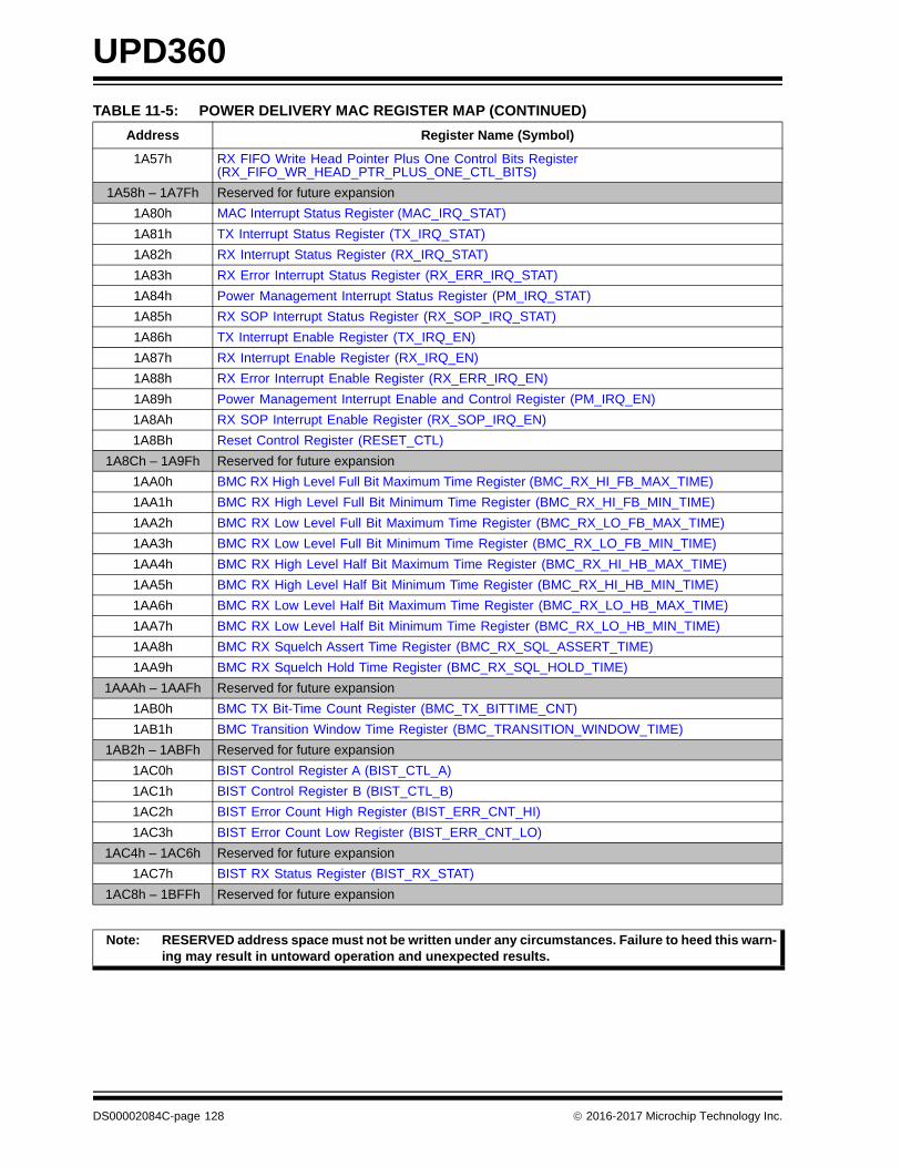
UPD360
1A57h RX FIFO Write Head Pointer Plus One Control Bits Register (RX_FIFO_WR_HEAD_PTR_PLUS_ONE_CTL_BITS)
1A58h – 1A7Fh Reserved for future expansion
1A80h MAC Interrupt Status Register (MAC_IRQ_STAT)
1A81h TX Interrupt Status Register (TX_IRQ_STAT)
1A82h RX Interrupt Status Register (RX_IRQ_STAT)
1A83h RX Error Interrupt Status Register (RX_ERR_IRQ_STAT)
1A84h Power Management Interrupt Status Register (PM_IRQ_STAT)
1A85h RX SOP Interrupt Status Register (RX_SOP_IRQ_STAT)
1A86h TX Interrupt Enable Register (TX_IRQ_EN)
1A87h RX Interrupt Enable Register (RX_IRQ_EN)
1A88h RX Error Interrupt Enable Register (RX_ERR_IRQ_EN)
1A89h Power Management Interrupt Enable and Control Register (PM_IRQ_EN)
1A8Ah RX SOP Interrupt Enable Register (RX_SOP_IRQ_EN)
1A8Bh Reset Control Register (RESET_CTL)
1A8Ch – 1A9Fh Reserved for future expansion
1AA0h BMC RX High Level Full Bit Maximum Time Register (BMC_RX_HI_FB_MAX_TIME)
1AA1h BMC RX High Level Full Bit Minimum Time Register (BMC_RX_HI_FB_MIN_TIME)
1AA2h BMC RX Low Level Full Bit Maximum Time Register (BMC_RX_LO_FB_MAX_TIME)
1AA3h BMC RX Low Level Full Bit Minimum Time Register (BMC_RX_LO_FB_MIN_TIME)
1AA4h BMC RX High Level Half Bit Maximum Time Register (BMC_RX_HI_HB_MAX_TIME)
1AA5h BMC RX High Level Half Bit Minimum Time Register (BMC_RX_HI_HB_MIN_TIME)
1AA6h BMC RX Low Level Half Bit Maximum Time Register (BMC_RX_LO_HB_MAX_TIME)
1AA7h BMC RX Low Level Half Bit Minimum Time Register (BMC_RX_LO_HB_MIN_TIME)
1AA8h BMC RX Squelch Assert Time Register (BMC_RX_SQL_ASSERT_TIME)
1AA9h BMC RX Squelch Hold Time Register (BMC_RX_SQL_HOLD_TIME)
1AAAh – 1AAFh Reserved for future expansion
1AB0h BMC TX Bit-Time Count Register (BMC_TX_BITTIME_CNT)
1AB1h BMC Transition Window Time Register (BMC_TRANSITION_WINDOW_TIME)
1AB2h – 1ABFh Reserved for future expansion
1AC0h BIST Control Register A (BIST_CTL_A)
1AC1h BIST Control Register B (BIST_CTL_B)
1AC2h BIST Error Count High Register (BIST_ERR_CNT_HI)
1AC3h BIST Error Count Low Register (BIST_ERR_CNT_LO)
1AC4h – 1AC6h Reserved for future expansion
1AC7h BIST RX Status Register (BIST_RX_STAT)
1AC8h – 1BFFh Reserved for future expansion
Note: RESERVED address space must not be written under any circumstances. Failure to heed this warn-ing may result in untoward operation and unexpected results.
TABLE 11-5: POWER DELIVERY MAC REGISTER MAP (CONTINUED)
Address Register Name (Symbol)
DS00002084C-page 128 2016-2017 Microchip Technology Inc.

UPD360
11.4.1 PD MAC TX REGISTERS
The following sub-sections describe the various registers associated with the PD MAC TX logic.
11.4.1.1 TX Control Register A (TX_CTL_A)
Address: 1A00h Size: 8 bits
Bits Description Type Default
7 RESERVED RO -
6 RETRY_ON_LINE_BUSYNormally hardware will abort a TX packet (including all retry attempts) if the line is Busy when hardware attempts to transmit the packet. (Note that trans-mission of GoodCRC ACK in response for Soft Reset is an exception to this, see the DIS_SPCL_SR_GCRC_ACK bit.)
Setting this bit will force hardware to not completely abort the transmission, but rather it will retry the packet up to N_RETRY_CNT times. Failure after N_RETRY_CNT times results in TX_FAILED status in the TX Interrupt Status Register (TX_IRQ_STAT) rather than a TX_ABORTED status.
The following conditions will still abort the TX packet:
• Hard reset received
• Cable reset received (if enabled and the SOP type of the pending TX is SOP', or SOP'', SOP'_Debug or SOP''_Debug)
• Good, non-duplicate, non-Ping, non-GoodCRC packet (including soft-reset) received with RX and TX SOP types matching or RX SOP type equaling SOP with TX SOP type not equaling SOP (can be disabled)
• Software sets the ABORT bit in the TX Control Register B (TX_CTL_B).
R/W 0b
5 DIS_SOP_ABRTS_NON_SOPNormally, when a SOP packet is received, a pending non-SOP packet (includ-ing wait for a GoodCRC) will be aborted. When this bit is set, a non-SOP packet will only be aborted by a packet with the same non-SOP type.
R/W 0b
4 DIS_SPCL_SR_GCRC_ACKDisable special treatment of GoodCRC ACK in response to Soft Reset.By default, in auto-response mode a line busy condition will not abort Good-CRC ACK transmission in response to Soft Reset reception. Setting this bit will disable this behavior and instead GoodCRC ACK transmission for Soft Reset will be processed the same as GoodCRC ACK for other packets.
Note: When this bit is set, the WAIT4LINE_IDLE bit will affect GoodCRCACK for Soft Reset as well.
R/W 0b
2016-2017 Microchip Technology Inc. DS00002084C-page 129
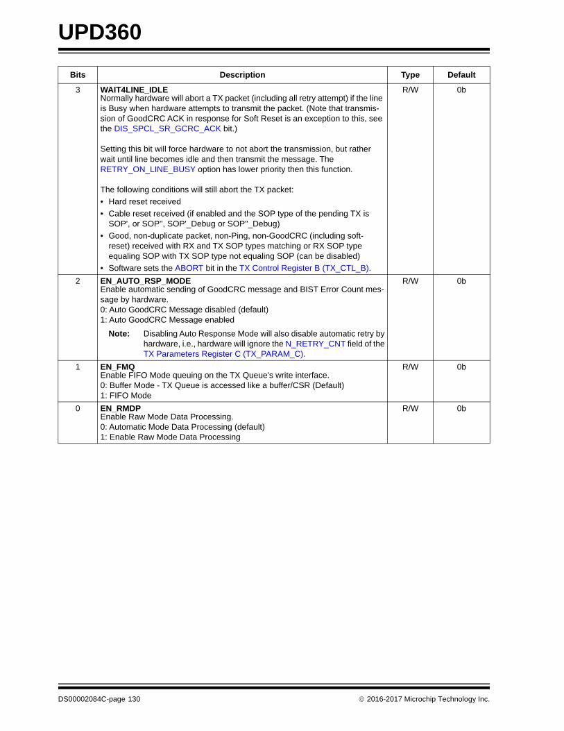
UPD360
3 WAIT4LINE_IDLENormally hardware will abort a TX packet (including all retry attempt) if the line is Busy when hardware attempts to transmit the packet. (Note that transmis-sion of GoodCRC ACK in response for Soft Reset is an exception to this, see the DIS_SPCL_SR_GCRC_ACK bit.)
Setting this bit will force hardware to not abort the transmission, but rather wait until line becomes idle and then transmit the message. The RETRY_ON_LINE_BUSY option has lower priority then this function.
The following conditions will still abort the TX packet:
• Hard reset received
• Cable reset received (if enabled and the SOP type of the pending TX is SOP', or SOP'', SOP'_Debug or SOP''_Debug)
• Good, non-duplicate packet, non-Ping, non-GoodCRC (including soft-reset) received with RX and TX SOP types matching or RX SOP type equaling SOP with TX SOP type not equaling SOP (can be disabled)
• Software sets the ABORT bit in the TX Control Register B (TX_CTL_B).
R/W 0b
2 EN_AUTO_RSP_MODEEnable automatic sending of GoodCRC message and BIST Error Count mes-sage by hardware.0: Auto GoodCRC Message disabled (default)1: Auto GoodCRC Message enabled
Note: Disabling Auto Response Mode will also disable automatic retry byhardware, i.e., hardware will ignore the N_RETRY_CNT field of theTX Parameters Register C (TX_PARAM_C).
R/W 0b
1 EN_FMQEnable FIFO Mode queuing on the TX Queue's write interface.0: Buffer Mode - TX Queue is accessed like a buffer/CSR (Default)1: FIFO Mode
R/W 0b
0 EN_RMDPEnable Raw Mode Data Processing.0: Automatic Mode Data Processing (default)1: Enable Raw Mode Data Processing
R/W 0b
Bits Description Type Default
DS00002084C-page 130 2016-2017 Microchip Technology Inc.

UPD360
11.4.1.2 TX Status Register (TX_STAT)
Address: 1A01h Size: 8 bits
Bits Description Type Default
7 RESERVED RO -
6:4 N_HW_RETRIESNumber of attempts by hardware to send a message successfully.
This field is automatically cleared when the GO bit in the TX Control Register B (TX_CTL_B) is set.
This field is meaningful only if a TX was successful. It is informational only.
0: Initial message was successful. This value must be correlated with the TX_ABORTED bit. If a TX message was aborted, this bit is meaningless.>0: Number of retries performed by the device. The maximum value depends on the N_RETRY_CNT field in the TX Parameters Register C (TX_PARAM_C) register.
RO 000b
3:1 RESERVED RO -
0 TX_ACTIVETransmitter is active.0: Transmitter is idle1: Transmitter is active
Software can monitor this bit to determine if transmission is in progress. De-assertion of this bit does not imply successful message transmission, only that the transmitter is no longer active and has stopped transmitting.
RO 0b
2016-2017 Microchip Technology Inc. DS00002084C-page 131
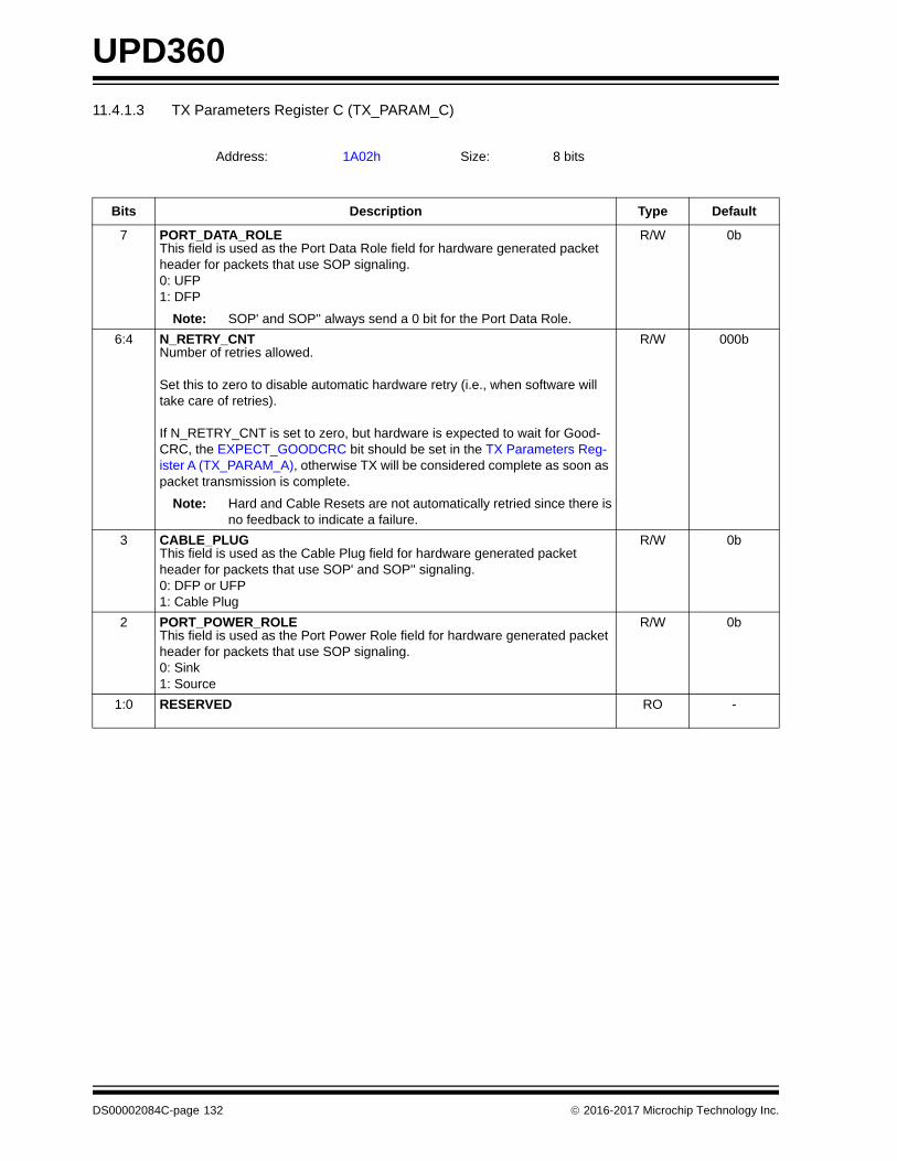
UPD360
11.4.1.3 TX Parameters Register C (TX_PARAM_C)
Address: 1A02h Size: 8 bits
Bits Description Type Default
7 PORT_DATA_ROLEThis field is used as the Port Data Role field for hardware generated packet header for packets that use SOP signaling.0: UFP1: DFP
Note: SOP' and SOP'' always send a 0 bit for the Port Data Role.
R/W 0b
6:4 N_RETRY_CNTNumber of retries allowed.
Set this to zero to disable automatic hardware retry (i.e., when software will take care of retries).
If N_RETRY_CNT is set to zero, but hardware is expected to wait for Good-CRC, the EXPECT_GOODCRC bit should be set in the TX Parameters Reg-ister A (TX_PARAM_A), otherwise TX will be considered complete as soon as packet transmission is complete.
Note: Hard and Cable Resets are not automatically retried since there isno feedback to indicate a failure.
R/W 000b
3 CABLE_PLUGThis field is used as the Cable Plug field for hardware generated packet header for packets that use SOP' and SOP'' signaling.0: DFP or UFP1: Cable Plug
R/W 0b
2 PORT_POWER_ROLEThis field is used as the Port Power Role field for hardware generated packet header for packets that use SOP signaling.0: Sink1: Source
R/W 0b
1:0 RESERVED RO -
DS00002084C-page 132 2016-2017 Microchip Technology Inc.

UPD360
11.4.1.4 TX Packet Length Register (TX_PKT_LEN)
11.4.1.5 TX Parameters Register A (TX_PARAM_A)
Address: 1A03h Size: 8 bits
Bits Description Type Default
7:6 RESERVED RO -
5:0 PKT_LENQueued packet length in bytes.Hardware uses this value in Auto Mode to determine when to insert the CRC.
PKT_LEN = bytes in header + bytes in data objects
Note: This applies to Auto Mode queue only and not to Raw Mode queue.Raw Mode queue has special code to insert CRC and terminatethe transmission.
Note: A value of '0' is invalid for this field.
R/W 000000b
Address: 1A04h Size: 8 bits
Bits Description Type Default
7 EXPECT_GOODCRCThis bit is used when the N_RETRY_CNT field in the TX Parameters Register C (TX_PARAM_C) is set to zero but hardware is expected to wait for Good-CRC in response to a TX message.
If N_RETRY_CNT is non-zero and EN_AUTO_RSP_MODE in the TX Control Register A (TX_CTL_A) is set, then hardware automatically waits for Good-CRC and this bit has no effect.
R/W 0b
6:4 TX_SOP_SELECTThis field selects the SOP used for normal TX packets, for Returned BIST Counters packets (in response to RX BIST Test Frames) and for TX BIST Test Frames.
This value is also used to verify the expected SOP type in the GoodCRC response when Auto retry is enabled.000: SOP001: SOP'010: SOP''011: SOP'_Debug100: SOP''_Debug101 - 111: Reserved
Note: For Auto retry mode, it is assumed that the expected SOP type isalso enabled in the RX Control Register B (RX_CTL_B).
R/W 000b
2016-2017 Microchip Technology Inc. DS00002084C-page 133
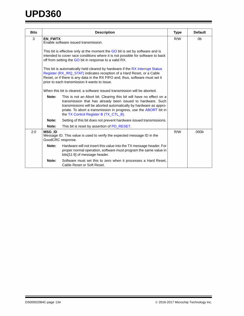
UPD360
3 EN_FWTXEnable software issued transmission.
This bit is effective only at the moment the GO bit is set by software and is intended to cover race conditions where it is not possible for software to back off from setting the GO bit in response to a valid RX.
This bit is automatically held cleared by hardware if the RX Interrupt Status Register (RX_IRQ_STAT) indicates reception of a Hard Reset, or a Cable Reset, or if there is any data in the RX FIFO and, thus, software must set it prior to each transmission it wants to issue.
When this bit is cleared, a software issued transmission will be aborted.
Note: This is not an Abort bit. Clearing this bit will have no effect on atransmission that has already been issued to hardware. Suchtransmissions will be aborted automatically by hardware as appro-priate. To abort a transmission in progress, use the ABORT bit inthe TX Control Register B (TX_CTL_B).
Note: Setting of this bit does not prevent hardware issued transmissions.
Note: This bit is reset by assertion of PD_RESET.
R/W 0b
2:0 MSG_IDMessage ID. This value is used to verify the expected message ID in the GoodCRC response.
Note: Hardware will not insert this value into the TX message header. Forproper normal operation, software must program the same value inbits[11:9] of message header.
Note: Software must set this to zero when it processes a Hard Reset,Cable Reset or Soft Reset.
R/W 000b
Bits Description Type Default
DS00002084C-page 134 2016-2017 Microchip Technology Inc.
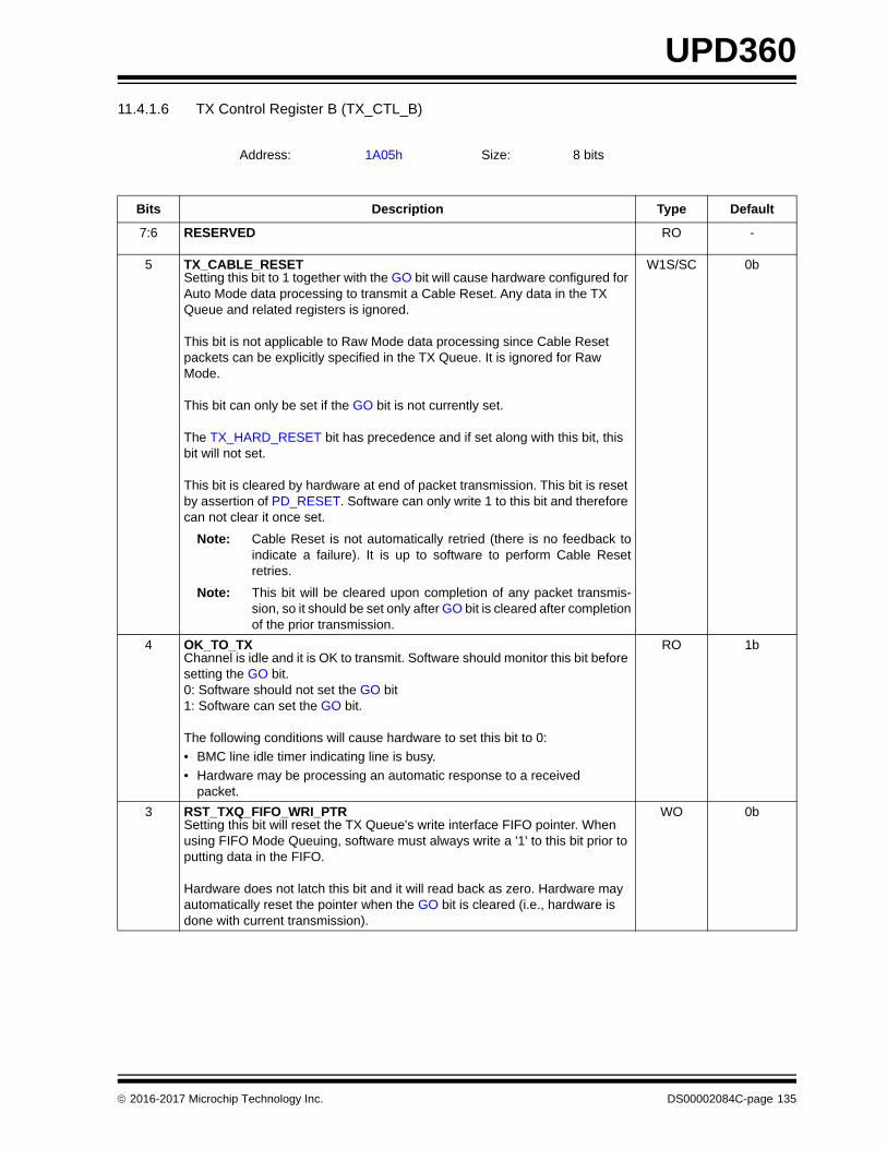
UPD360
11.4.1.6 TX Control Register B (TX_CTL_B)
Address: 1A05h Size: 8 bits
Bits Description Type Default
7:6 RESERVED RO -
5 TX_CABLE_RESETSetting this bit to 1 together with the GO bit will cause hardware configured for Auto Mode data processing to transmit a Cable Reset. Any data in the TX Queue and related registers is ignored.
This bit is not applicable to Raw Mode data processing since Cable Reset packets can be explicitly specified in the TX Queue. It is ignored for Raw Mode.
This bit can only be set if the GO bit is not currently set.
The TX_HARD_RESET bit has precedence and if set along with this bit, this bit will not set.
This bit is cleared by hardware at end of packet transmission. This bit is reset by assertion of PD_RESET. Software can only write 1 to this bit and therefore can not clear it once set.
Note: Cable Reset is not automatically retried (there is no feedback toindicate a failure). It is up to software to perform Cable Resetretries.
Note: This bit will be cleared upon completion of any packet transmis-sion, so it should be set only after GO bit is cleared after completionof the prior transmission.
W1S/SC 0b
4 OK_TO_TXChannel is idle and it is OK to transmit. Software should monitor this bit before setting the GO bit.0: Software should not set the GO bit1: Software can set the GO bit.
The following conditions will cause hardware to set this bit to 0:
• BMC line idle timer indicating line is busy.
• Hardware may be processing an automatic response to a received packet.
RO 1b
3 RST_TXQ_FIFO_WRI_PTRSetting this bit will reset the TX Queue's write interface FIFO pointer. When using FIFO Mode Queuing, software must always write a '1' to this bit prior to putting data in the FIFO.
Hardware does not latch this bit and it will read back as zero. Hardware may automatically reset the pointer when the GO bit is cleared (i.e., hardware is done with current transmission).
WO 0b
2016-2017 Microchip Technology Inc. DS00002084C-page 135

UPD360
2 TX_HARD_RESETSetting this bit to 1 together with the GO bit will cause hardware configured for Auto Mode data processing to transmit a Hard Reset. Any data in the TX Queue and related registers is ignored.
This bit is not applicable to Raw Mode data processing since a Hard Reset packet can be explicitly specified in the TX Queue. It is ignored for Raw Mode.
This bit can only be set if the GO bit is not currently set.
This bit is cleared by hardware at end of packet transmission. This bit is reset by assertion of PD_RESET. Software can only write 1 to this bit and therefore can not clear it once set.
Note: Hard Reset is not automatically retried (there is no feedback to indi-cate a failure). It is up to software to perform Hard Reset retries.
Note: This bit will be cleared upon completion of any packet transmis-sion, so it should be set only after the GO bit is cleared after com-pletion of the prior transmission.
W1S/SC 0b
1 ABORTSetting this bit will abort the current transmission in progress as soon as pos-sible. Writing a '0' has not effect.
Hardware does not latch this bit and it will read back as zero.
Hardware will finish the current nibble transmission, send EOP, and then ter-minate transmission. If this bit is set during preamble phase, then the current bit of the preamble will be completed prior to termination.
Software should use the TX_EOP status bit in the TX Interrupt Status Register (TX_IRQ_STAT) to determine when the current packet has been terminated.
WO 0b
0 GOWriting a 1 to this bit will:
• Start transmission of the packet in the TX queue on to the wire or:
• Send Hard Reset if the TX_HARD_RESET bit of this register is set and data processing mode is set to Auto (i.e., the EN_RMDP bit in the TX Control Register A (TX_CTL_A) is not set).
• Send Cable Reset if the TX_CABLE_RESET bit of this register is set and data processing mode is set to Auto (i.e., the EN_RMDP bit in the TX Control Register A (TX_CTL_A) is not set).
Hardware will clear this bit when transmission is complete. This bit is reset by assertion of PD_RESET. Software can only write 1 to this bit and therefore can not clear it once set. Clearing of this bit by hardware does not indicate the message was sent successfully.
Hardware may detect bus collision and abort transmission. In this case, the TX_ABORTED bit in the TX Interrupt Status Register (TX_IRQ_STAT) will be set and an interrupt to MCU will be generated.
W1S/SC 0b
Bits Description Type Default
DS00002084C-page 136 2016-2017 Microchip Technology Inc.
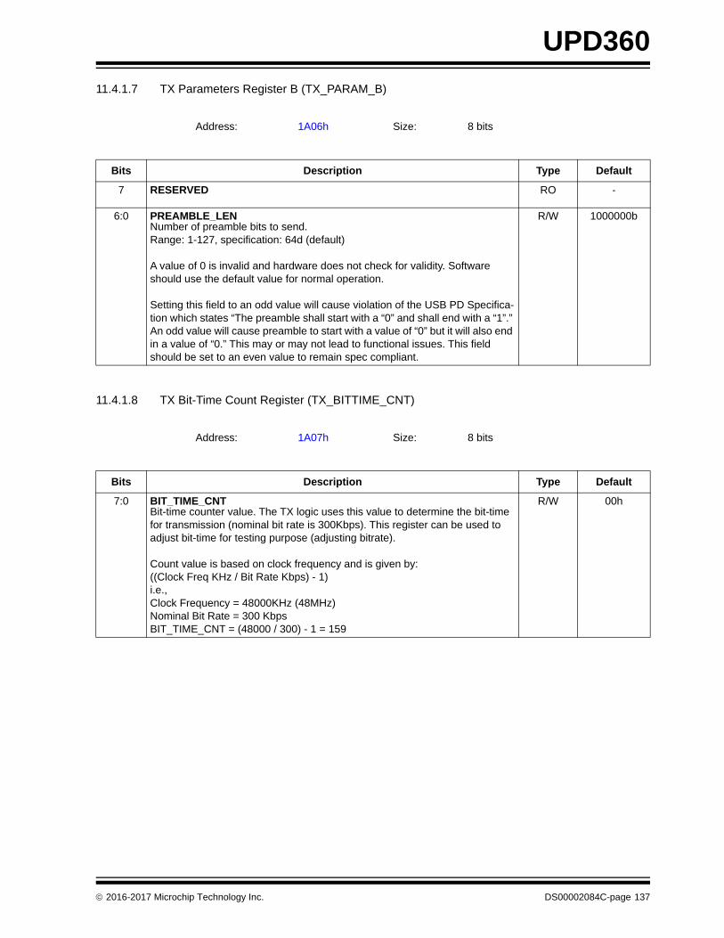
UPD360
11.4.1.7 TX Parameters Register B (TX_PARAM_B)
11.4.1.8 TX Bit-Time Count Register (TX_BITTIME_CNT)
Address: 1A06h Size: 8 bits
Bits Description Type Default
7 RESERVED RO -
6:0 PREAMBLE_LENNumber of preamble bits to send.Range: 1-127, specification: 64d (default)
A value of 0 is invalid and hardware does not check for validity. Software should use the default value for normal operation.
Setting this field to an odd value will cause violation of the USB PD Specifica-tion which states “The preamble shall start with a “0” and shall end with a “1”.” An odd value will cause preamble to start with a value of “0” but it will also end in a value of “0.” This may or may not lead to functional issues. This field should be set to an even value to remain spec compliant.
R/W 1000000b
Address: 1A07h Size: 8 bits
Bits Description Type Default
7:0 BIT_TIME_CNTBit-time counter value. The TX logic uses this value to determine the bit-time for transmission (nominal bit rate is 300Kbps). This register can be used to adjust bit-time for testing purpose (adjusting bitrate).
Count value is based on clock frequency and is given by:((Clock Freq KHz / Bit Rate Kbps) - 1)i.e.,Clock Frequency = 48000KHz (48MHz)Nominal Bit Rate = 300 KbpsBIT_TIME_CNT = (48000 / 300) - 1 = 159
R/W 00h
2016-2017 Microchip Technology Inc. DS00002084C-page 137

UPD360
11.4.1.9 TX Turnaround Time Register (TX_TA_TIME)
This register controls the IFG timer.
11.4.1.10 TX Abort Status Register (TX_ABORT_STAT)
This field is used in conjunction with the TX_ABORTED interrupt and provides details for why the TX was aborted. Bitsin this register are sticky, i.e., once any bit is set by hardware this field cannot be updated by hardware until softwareclears the field.
Address: 1A08h Size: 8 bits
Bits Description Type Default
7:6 RESERVED RO -
5:0 TA_TIMETurnaround time in us.Range: 1-63, specification: 25us
A value of 0 is invalid and hardware does not check for validity.
Hardware uses a free running 1us pulse generator, thus, the value of this field should be 1 more than desired to ensure the minimum time (26d).
R/W 010101b
Address: 1A09h Size: 8 bits
Note: Bits in this register are set by hardware and must be cleared by software. The bits are not mutually exclu-sive, i.e., more than one bit may be set depending on the circumstance.
Bits Description Type Default
7 TX_ABORT_STAT[7]While waiting for GoodCRC, TX aborted due to Protocol Error (i.e., received other than GoodCRC or Ping message while waiting for GoodCRC or Receiv-ing a Hard or Cable Reset.)
R/W1C 0b
6 TX_ABORT_STAT[6]During software issued TX, TX was aborted due to RX (including Hard or Cable Reset) while waiting for bus turnaround or waiting for line to go idle.
R/W1C 0b
5 TX_ABORT_STAT[5]Auto-retry aborted due to RX (including Hard or Cable Reset) while waiting for bus turnaround or while waiting for line to go idle.
R/W1C 0b
4 TX_ABORT_STAT[4]Auto-retry aborted due to line being busy after bus turnaround.
R/W1C 0b
3 RESERVED RO -
2 TX_ABORT_STAT[2]During software issued TX, line was busy after bus turnaround.
R/W1C 0b
1 TX_ABORT_STAT[1]Software issued abort while software issued TX was in process.
R/W1C 0b
0 TX_ABORT_STAT[0]Software issued GO with TX disabled.
R/W1C 0b
DS00002084C-page 138 2016-2017 Microchip Technology Inc.

UPD360
11.4.1.11 TX Auto-Response Abort Status Register (TX_AR_ABORT_STAT)
This field is used in conjunction with the AUTO_RSP_ABORTED interrupt and provides details for why the TX wasaborted. Bits in this register are sticky, i.e., once any bit is set by hardware this field cannot be updated by hardwareuntil software clears the field.
11.4.1.12 TX Power Up Time Register (TX_POWER_UP_TIME)
Address: 1A0Ah Size: 8 bits
Note: Bits in this register are set by hardware and must be cleared by software. The bits are not mutually exclu-sive, i.e., more than one bit may be set depending on the circumstance.
Bits Description Type Default
7 RESERVED RO -
6 TX_AR_ABORT_STAT[6]Auto-response aborted due to RX (including Hard or Cable Reset) while wait-ing for bus turnaround or while waiting for line to go idle.
R/W1C 0b
5:4 RESERVED RO -
3 TX_AR_ABORT_STAT[3]Line was busy after bus turnaround time during auto-response.
R/W1C 0b
2 RESERVED RO -
1 TX_AR_ABORT_STAT[1]Software issued abort while auto-response was in process.
R/W1C 0b
0 RESERVED RO -
Address: 1A0Bh Size: 8 bits
Bits Description Type Default
7:0 TX_POWER_UP_TIMETX Power Up Time before transmitting (unit is 8 clock cycles).Range: 0-255 (Actual time is 5 clocks larger.)
The analog requires a minimum time of 5us to power up.
Count value is based on clock frequency and is given by:TX_POWER_UP_TIME = power up time uS x Clock Freq MHz / 8i.e.,Clock Frequency = 48MHzpower up time = 5 uSTX_POWER_UP_TIME = 5 x 48 / 8 = 30
R/W 00h
2016-2017 Microchip Technology Inc. DS00002084C-page 139
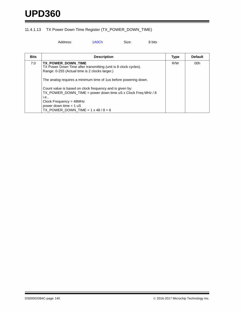
UPD360
11.4.1.13 TX Power Down Time Register (TX_POWER_DOWN_TIME)
Address: 1A0Ch Size: 8 bits
Bits Description Type Default
7:0 TX_POWER_DOWN_TIMETX Power Down Time after transmitting (unit is 8 clock cycles).Range: 0-255 (Actual time is 2 clocks larger.)
The analog requires a minimum time of 1us before powering down.
Count value is based on clock frequency and is given by:TX_POWER_DOWN_TIME = power down time uS x Clock Freq MHz / 8i.e.,Clock Frequency = 48MHzpower down time = 1 uSTX_POWER_DOWN_TIME = 1 x 48 / 8 = 6
R/W 00h
DS00002084C-page 140 2016-2017 Microchip Technology Inc.

UPD360
11.4.2 PD MAC RX REGISTERS
The following sub-sections describe the various registers associated with the PD MAC RX logic.
11.4.2.1 RX Control Register A (RX_CTL_A)
Address: 1A40h Size: 8 bits
Bits Description Type Default
7:6 RESERVED RO -
5 EN_LOOPBACKEnable loopback. This bit allows the MAC to receive its own transmission.
Note: Loopback happens at the pin where TX and RX are connectedtogether.
R/W 0b
4 EN_RCVEnable Receiver. Software should set this bit when it is done configuring the receiver. Setting this bit will enable the receiver to start normal operation.
If this bit is set while receive activity is in progress it will take effect after cur-rent receive activity is over. If this bit is cleared while a receive is being pro-cessed it will take effect after current receive is finished.
This bit will be automatically cleared by hardware upon reception of Hard Reset or a Cable Reset to prevent normal packet reception.
After POR or SW_RESET, Hard and Cable Reset reception is disabled until EN_RCV is set. Thereafter, clearing of EN_RCV (by software or hardware) has no impact to reception of Hard or Cable Reset, i.e., hardware will process Hard or Cable Reset even with EN_RCV cleared.
If software wishes to re-initialize receive timing parameters after EN_RCV has been set once it must first reset the UPD_MAC_v2 using SW_RESET.This bit is not reset by assertion of PD_RESET.
R/W 0b
3 RST_RECEIVERSetting this bit will reset the receiver Queue. Software should set this bit if receiver hardware may be out of sync with software. Hardware latches this bit so it must be cleared by software to resume receiver operation. Receiver hardware is also reset when PD_RESET bit in RESET_CTL register is set.
R/W 0b
2016-2017 Microchip Technology Inc. DS00002084C-page 141
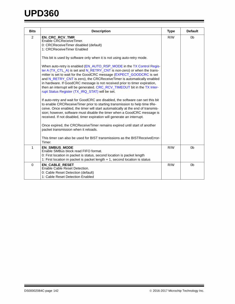
UPD360
2 EN_CRC_RCV_TMREnable CRCReceiveTimer.0: CRCReceiveTimer disabled (default)1: CRCReceiveTimer Enabled
This bit is used by software only when it is not using auto-retry mode.
When auto-retry is enabled (EN_AUTO_RSP_MODE in the TX Control Regis-ter A (TX_CTL_A) is set and N_RETRY_CNT is non-zero) or when the trans-mitter is set to wait for the GoodCRC message (EXPECT_GOODCRC is set and N_RETRY_CNT is zero), the CRCReceiveTimer is automatically enabled in hardware. If GoodCRC message is not received prior to timer expiration, then an interrupt will be generated. CRC_RCV_TIMEOUT bit in the TX Inter-rupt Status Register (TX_IRQ_STAT) will be set.
If auto-retry and wait for GoodCRC are disabled, the software can set this bit to enable CRCReceiveTimer prior to starting transmission to help time tRe-ceive. Once enabled, the timer will start automatically at the end of transmis-sion; however, software must disable the timer when a GoodCRC message is received. If not disabled, timer expiration will generate an interrupt.
Once expired, the CRCReceiveTimer remains expired until start of another packet transmission when it reloads.
This timer can also be used for BIST transmissions as the BISTReceiveError-Timer.
R/W 0b
1 EN_SMBUS_MODEEnable SMBus block read FIFO format. 0: First location in packet is status, second location is packet length1: First location in packet is packet length + 1, second location is status
R/W 0b
0 EN_CABLE_RESETEnable Cable Reset Detection.0: Cable Reset Detection (default)1: Cable Reset Detection Enabled
R/W 0b
Bits Description Type Default
DS00002084C-page 142 2016-2017 Microchip Technology Inc.
UPD360
11.4.2.2 RX Control Register B (RX_CTL_B)
11.4.2.3 RX Maximum Bit-Rate Bit Period Count Register (RX_BIT_PER_CNT_MAX_BR)
The value of this register, together with value of the RX Minimum Bit-Rate Bit Period Count Register(RX_BIT_PER_CNT_MIN_BR), is used to determine valid bit-time (also referenced as bit-period) of the RX signal.
RX_BIT_PER_CNT_MIN_BR > valid bit time > RX_BIT_PER_CNT_MAX_BR.
Address: 1A41h Size: 8 bits
Bits Description Type Default
7 RESERVED RO -
6:2 RX_SOP_ENABLESOP Types enabled to be received. Includes RX BIST Test Frames.Bit 2 - SOPBit 3 - SOP'Bit 4 - SOP''Bit 5 - SOP'_Debug Bit 6 - SOP''_DebugSoftware is allowed to change the field at any time. An internal copy is held during active receive and updated from the register during idle time
R/W 00001b
1:0 RESERVED RO -
Address: 1A42h Size: 8 bits
Bits Description Type Default
7:0 RX_BIT_PER_CNT_MAX_BRBit period count at maximum bit-rate.= (((clock_freq_KHz / max_bit_rate_Kbps) * (100 - tolerance) / 100) - 1)
WARNING: If macros are defined in C code, then math must be arranged so that integer overflow does not occur.
R/W 00h
2016-2017 Microchip Technology Inc. DS00002084C-page 143

UPD360
11.4.2.4 RX Minimum Bit-Rate Bit Period Count Register (RX_BIT_PER_CNT_MIN_BR)
The value of this register, together with value of the RX Maximum Bit-Rate Bit Period Count Register(RX_BIT_PER_CNT_MAX_BR), is used to determine valid bit-time (also referenced as bit-period) of the RX signal.
RX_BIT_PER_CNT_MIN_BR > valid bit time > RX_BIT_PER_CNT_MAX_BR.
11.4.2.5 RX Status Register (RX_STAT)
Address: 1A43h Size: 8 bits
Bits Description Type Default
7:0 RX_BIT_PER_CNT_MIN_BRBit period count at minimum bit-rate.= (((clock_freq_KHz / min_bit_rate_Kbps) * (100 + tolerance) / 100) - 1)
WARNING: If macros are defined in C code, then math must be arranged so that integer overflow does not occur.
R/W 00h
Address: 1A44h Size: 8 bits
Bits Description Type Default
7:2 RESERVED RO -
1 RX_IN_PROCESSReceiver is active.Hardware is receiving a packet, i.e., line is busy and transmitter is not active.
RO 0b
0 LINE_STATE0: Line is idle1: Line is busy (BMC line idle timer indicating line is busy)
If this bit is “1”, a receive might be in progress and software should wait for the message reception to complete. If it is “0”, software may set the GO bit.
Hardware will take further action until the very last possible moment to avoid bus contention. Bus contention is still possible and not 100% avoidable.
In cases where hardware takes preventative measures to avoid bus conten-tion, the TX packet will be aborted. Software will be informed of this via an interrupt and setting of the TX_ABORTED bit in the TX Interrupt Status Regis-ter (TX_IRQ_STAT).
RO 0b
DS00002084C-page 144 2016-2017 Microchip Technology Inc.
UPD360
11.4.2.6 RX Packet Status Register (RX_PKT_STAT)
This register is applicable only when using auto-response/retry modes. This register is used in conjunction with the fol-lowing bits to provide additional information regarding the status of a received packet:
• RX_DONE bit in the RX Interrupt Status Register (RX_IRQ_STAT)
• RX_PCOL_ERROR bit in the RX Error Interrupt Status Register (RX_ERR_IRQ_STAT)
• RX_PKT_DROPPED bit in the RX Error Interrupt Status Register (RX_ERR_IRQ_STAT)
• RX_BUF_OVR_RUN bit in the RX Error Interrupt Status Register (RX_ERR_IRQ_STAT)
Bits in this register are sticky, i.e., once any bit is set by hardware this field cannot be updated by hardware until softwareclears the field.
A value of 0x00 indicates no errors, while a value of 0xFF indicates that the packet status is currently unknown. Othervalues are interpreted as specified in the bit definitions for this register.
Address: 1A45h Size: 8 bits
Note: There no status for having received a GoodCRC message with matching MSG_ID. Successful completionof a TX is indication that a valid GoodCRC ACK was received.
Note: Bits in this register are set by hardware and must be cleared by software. The bits are not mutually exclu-sive, i.e., more than one bit may be set depending on the circumstance.
Bits Description Type Default
7 RESERVED RO -
6 RX_PKT_STAT[6]ODD_NIBBLES. Received packet dropped because it had odd number of nib-bles in data phase. Not set if RX_PKT_STAT[3] (RX_OVER_SIZE) is set regardless of bad CRC, symbol errors or odd nibbles. RX_BAD_PKT interrupt is asserted.
R/W1C 0b
5 RX_PKT_STAT[5]SYM_ERROR. There was a symbol error in packet but BAD_CRC was not reported. Not set if RX_PKT_STAT[3] (RX_OVER_SIZE) is set regardless of bad CRC, symbol errors or odd nibbles. RX_BAD_PKT interrupt is asserted.
R/W1C 0b
4 RX_PKT_STAT[4]RX_FIFO_FULL. Received packet had to be dropped because the FIFO was full either at SOP or during data. RX_BUF_OVR_RUN interrupt is asserted.
R/W1C 0b
3 RX_PKT_STAT[3]RX_OVER_SIZE. Received packet had to be dropped because it was larger than the maximum size set in the RX Maximum Packet Size Register. RX_BAD_PKT interrupt is asserted.
R/W1C 0b
2 RX_PKT_STAT[2]PCOL_ERROR. Received other than GoodCRC or Ping message when GoodCRC was expected. RX_PCOL_ERROR interrupt is asserted.
R/W1C 0b
1 RX_PKT_STAT[1]DUPLICATE_PACKET. Applicable to auto-response mode. RX_PKT_-DROPPED interrupt is asserted.
R/W1C 0b
0 RX_PKT_STAT[0]BAD_CRC. RX packet had bad CRC. RX_BAD_PKT interrupt is asserted. This bit is also forced set if symbol error or odd nibble count occurs. It is not set if RX_PKT_STAT[3] (RX_OVER_SIZE) is set, regardless of bad CRC, symbol errors or odd nibbles.
R/W1C 0b
2016-2017 Microchip Technology Inc. DS00002084C-page 145

UPD360
11.4.2.7 RX tReceive Time Register (RX_TRECEIVE_TIME)
11.4.2.8 RX BadCRC Packet Count Register (RX_BADCRC_PKT_CNT)
This register keeps track of the number of packets received with bad CRC (any packet with valid SOP but bad CRC orinvalid EOP or symbol error). This register is for debug purpose only.
If enabled, an interrupt can be generated when the count of this register reaches 128.
Address: 1A46h Size: 8 bits
Bits Description Type Default
7:0 TRECEIVECRCReceiveTimer timeout value (tReceive) in 10's of micro seconds.
Timeout value = field value * 10 (us)
Range: 0-255, specification: 900-1100us (90-110)
Note: A value of 0 is invalid and hardware does not check for validity.
Note: Hardware uses a free running 1us pulse generator, thus, thisCRCReceiveTimer may be 1us less than that expected.
Note: Reset value is programmed to be 1000us (+/- 2%).
R/W 64h
Address: 1A47h Size: 8 bits
Bits Description Type Default
7:0 BADCRC_PKT_CNTNumber of bad packets received, i.e., with Bad CRC or invalid EOP or symbol error.
When the value of this register becomes greater than 127, the DBG_EVENT bit in the RX Interrupt Status Register (RX_IRQ_STAT) will be set.
Any write to this register will clear all bits.
Note: This register is not affected by packets received during BISTReceiver Test. All these packets will be corrupted.
R/WAC 00h
DS00002084C-page 146 2016-2017 Microchip Technology Inc.

UPD360
11.4.2.9 RX Duplicate Packet Count Register (RX_DUP_PKT_CNT)
This register keeps track of the number of the number of duplicate packets received. It is applicable only when AutomaticResponse Mode is enabled. This register is for debug purpose only.
If enabled, an interrupt can be generated when the count of this register reaches 128.
11.4.2.10 RX Hard Reset Detection Window Register (RX_HR_DET_WINDOW)
11.4.2.11 RX Last GoodCRC Packet High Byte Register (RX_LAST_GCRC_PKT_HI)
Address: 1A48h Size: 8 bits
Bits Description Type Default
7:0 DUP_PKT_CNTNumber of duplicate packets received. Applicable when Auto Response Mode is enabled.
When the value of this register becomes greater than 127, the DBG_EVENT bit in the RX Interrupt Status Register (RX_IRQ_STAT) will be set.
Any write to this register will clear all bits.
R/WAC 00h
Address: 1A49h Size: 8 bits
Bits Description Type Default
7 RESERVED RO -
6:0 RX_HR_DET_WINDOWValue of Hard Reset detection window in number of bits.This field determines when a detected Hard Reset or Cable Reset will be con-sidered valid.
R/W 1011110b
Address: 1A4Ah Size: 8 bits
Bits Description Type Default
7:0 RX_LAST_GCRC_PKT_HIBits [15:8] of received GoodCRC message.
This register is only valid when auto-retry is enabled. Since GoodCRC mes-sage in auto-retry mode is not stored in the RX queue, this register provides a means for software to examine the last GoodCRC message received.
RO 00h
2016-2017 Microchip Technology Inc. DS00002084C-page 147

UPD360
11.4.2.12 RX Last GoodCRC Packet Low Byte Register (RX_LAST_GCRC_PKT_LO)
11.4.2.13 RX Message ID Stored Register (RX_MSG_ID_STORED)
This register indicates if a last message ID was stored for each SOP type. A write to the appropriate bit will clear thelast stored message ID for the SOP type indicated. When cleared, the next packet received for the SOP type will not beconsidered a duplicate. Software should clear the appropriate bit when it processes a Soft Reset.
Bits in this register are set by hardware and must be cleared by software.
This register is also cleared when software issues a SW_RESET or PD_RESET via the Reset Control Register(RESET_CTL).
11.4.2.14 RX Maximum Packet Size Register (RX_MAX_SIZE)
The value of this register sets the maximum receive packet size, including the 4 bytes of CRC.
Address: 1A4Bh Size: 8 bits
Bits Description Type Default
7:0 RX_LAST_GCRC_PKT_LOBits [7:0] of received GoodCRC message.
This register is only valid when auto-retry is enabled. Since GoodCRC mes-sage in auto-retry mode is not stored in the RX queue, this register provides a means for software to examine the last GoodCRC message received.
RO 00h
Address: 1A4Ch Size: 8 bits
Bits Description Type Default
7:5 RESERVED RO -
4:0 RX_MSG_ID_STOREDThis field indicates that a last message ID was stored for the SOP type.Bit 0: SOPBit 1: SOP'Bit 2: SOP''Bit 3: SOP'_DebugBit 4: SOP''_Debug
W1C 00000b
Address: 1A4Dh Size: 8 bits
Bits Description Type Default
7:0 RX_MAX_SIZEMaximum receive packet size including the 4 byte CRC.
R/W 22h
DS00002084C-page 148 2016-2017 Microchip Technology Inc.
UPD360
11.4.2.15 RX FIFO Read Pointer Register (RX_FIFO_RD_PTR)
This register contains the RX FIFO read pointer. Software may update this register to flush a packet based on the knownpacket length and starting point.
Software must keep the RX FIFO Read Pointer Control Bits Register coherent with this register if software were toupdate this register.
In order to maintain coherency, writes to this register are held in a temporary register and are transferred to the actualregister when the RX FIFO Read Pointer Control Bits Register is written.
11.4.2.16 RX FIFO Read Pointer Control Bits Register (RX_FIFO_RD_PTR_CTL_BITS)
This register contains the auxiliary control bits of the RX FIFO read pointer.
Software must keep these bits coherent with the RX FIFO Read Pointer if software were to update the latter.
Address: 1A50h Size: 8 bits
Bits Description Type Default
7 RESERVED RO -
6:0 RX_FIFO_RD_PTRThis field contains the RX FIFO read pointer.
R/W 0000000b
Address: 1A51h Size: 8 bits
Bits Description Type Default
7 RX_FIFO_EMPTYThis field indicates that the RX FIFO is empty (RX FIFO Write Head Pointer equals the RX FIFO Read Pointer.)
RO 1b
6:2 RESERVED RO -
1 RX_FIFO_RD_PTR_AT_TOPThis field indicates that the RX FIFO read pointer is at the top of the RAM (location 127).
RO 0b
0 RX_FIFO_RX_PTR_WRAPThis field toggles each time the RX FIFO read pointer wraps past the top of the RAM (location 127). If software updates the RX FIFO read pointer such that it wraps, this bit must be toggled.
R/W 0b
2016-2017 Microchip Technology Inc. DS00002084C-page 149
UPD360
11.4.2.17 RX FIFO Write Current Pointer Register (RX_FIFO_WR_CURRENT_PTR)
This register contains the RX FIFO write current pointer. This pointer indicates where the next received byte of data willbe stored. This register is for debug and test purpose only and should not normally be written.
Software must maintain coherency between this and the other Write Pointer Registers.
There is no hardware holding register to maintain write coherency between this and the other Write Pointer Registers.It is assumed that this register is only written while there is no active receive.
11.4.2.18 RX FIFO Write Current Pointer Control Bits Register (RX_FIFO_WR_CURRENT_PTR_CTL_BITS)
This register contains the auxiliary control bits of the RX FIFO write current pointer. This register is for debug and testpurpose only and should not normally be written.
Software must maintain coherency between this and the other Write Pointer Registers.
There is no hardware holding register to maintain write coherency between this and the other Write Pointer Registers.It is assumed that this register is only written while there is no active receive.
Address: 1A52h Size: 8 bits
Bits Description Type Default
7 RESERVED RO -
6:0 RX_FIFO_WR_CURRENT_PTRThis field contains the RX FIFO write current pointer.
R/W 0000000b
Address: 1A53h Size: 8 bits
Bits Description Type Default
7 RX_FIFO_FULLThis field indicates that the RX FIFO is full (RX FIFO Write Current Pointer equals the RX FIFO Read Pointer.)
RO 0b
6:2 RESERVED RO -
1 RX_FIFO_WR_CURRENT_PTR_AT_TOPThis field indicates that the RX FIFO write current pointer is at the top of the RAM (location 127).
RO 0b
0 RX_FIFO_WR_CURRENT_PTR_WRAPThis field toggles each time the RX FIFO write current pointer wraps past the top of the RAM (location 127).
R/W 0b
DS00002084C-page 150 2016-2017 Microchip Technology Inc.

UPD360
11.4.2.19 RX FIFO Write Head Pointer Register (RX_FIFO_WR_HEAD_PTR)
This register contains the RX FIFO write head pointer. This pointer indicates where the next received packet starts. Thisregister is for debug and test purpose only and should not normally be written.
Software must maintain coherency between this and the other Write Pointer Registers.
There is no hardware holding register to maintain write coherency between this and the other Write Pointer Registers.It is assumed that this register is only written while there is no active receive.
11.4.2.20 RX FIFO Write Head Pointer Control Bits Register (RX_FIFO_WR_HEAD_PTR_CTL_BITS)
This register contains the auxiliary control bits of the RX FIFO write head pointer. This register is for debug and testpurpose only and should not normally be written.
Software must maintain coherency between this and the other Write Pointer Registers.
There is no hardware holding register to maintain write coherency between this and the other Write Pointer Registers.It is assumed that this register is only written while there is no active receive.
Address: 1A54h Size: 8 bits
Bits Description Type Default
7 RESERVED RO -
6:0 RX_FIFO_WR_HEAD_PTRThis field contains the RX FIFO write head pointer.
R/W 0000000b
Address: 1A55h Size: 8 bits
Bits Description Type Default
7 RX_FIFO_NO_ROOM_FOR_HEADERThis field indicates that the RX FIFO has no space for the RX header (status and length) (RX FIFO Write Head Pointer equals the RX FIFO Read Pointer or RX FIFO Write Head Pointer Plus One equals the RX FIFO Read Pointer).
RO 0b
6:3 RESERVED RO -
2 RX_FIFO_WR_HEAD_PTR_AT_2ND_FROM _TOPThis field indicates that the RX FIFO write head pointer is one below the top of the RAM (location 126).
RO 0b
1 RX_FIFO_WR_HEAD_PTR_AT_TOPThis field indicates that the RX FIFO write head pointer is at the top of the RAM (location 127).
RO 0b
0 RX_FIFO_WR_HEAD_PTR_WRAPThis field toggles each time the RX FIFO write head pointer wraps past the top of the RAM (location 127).
R/W 0b
2016-2017 Microchip Technology Inc. DS00002084C-page 151
UPD360
11.4.2.21 RX FIFO Write Head Pointer Plus One Register (RX_FIFO_WR_HEAD_PTR_PLUS_ONE)
This register contains the RX FIFO write head pointer plus one. This pointer indicates where the next received packetstarts plus one. This register is for debug and test purpose only and should not normally be written.
Software must maintain coherency between this and the other Write Pointer Registers.
There is no hardware holding register to maintain write coherency between this and the other Write Pointer Registers.It is assumed that this register is only written while there is no active receive.
11.4.2.22 RX FIFO Write Head Pointer Plus One Control Bits Register (RX_FIFO_WR_HEAD_PTR_PLUS_ONE_CTL_BITS)
This register contains the auxiliary control bits of the RX FIFO write head pointer plus one. This register is for debug andtest purpose only and should not normally be written.
Software must maintain coherency between this and the other Write Pointer Registers.
There is no hardware holding register to maintain write coherency between this and the other Write Pointer Registers.It is assumed that this register is only written while there is no active receive.
Address: 1A56h Size: 8 bits
Bits Description Type Default
7 RESERVED RO -
6:0 RX_FIFO_WR_HEAD_PTR_PLUS_ONEThis field contains the RX FIFO write head pointer plus one.
R/W 0000001b
Address: 1A57h Size: 8 bits
Bits Description Type Default
7:1 RESERVED RO -
0 RX_FIFO_WR_HEAD_PTR_PLUS_ONE_WRAPThis field toggles each time the RX FIFO write head pointer plus one wraps past the top of the RAM (location 127).
R/W 0b
DS00002084C-page 152 2016-2017 Microchip Technology Inc.
UPD360
11.4.3 PD MAC INTERRUPT STATUS AND ENABLE REGISTERS
The following sub-sections describe the various registers associated with the PD MAC interrupts.
Refer to Section 8.1, "System Interrupts," on page 35 for additional information on system level interrupt control.
11.4.3.1 MAC Interrupt Status Register (MAC_IRQ_STAT)
This register reflects the summary status of the various interrupt sources. If any of these bits are set, the MAC_INT inter-rupt bit in the Interrupt Status Register (INT_STS) will be active (if enabled).
Bits in this register are read only and reflect the combined result of the other PD MAC interrupt status registers.
There is no corresponding enable register, since all interrupts have enables at lower levels of the hierarchy.
Address: 1A80h Size: 8 bits
Bits Description Type Default
7:5 RESERVED RO -
4 RX_SOP_IRQ_STATRX SOP status. This bit is set when any bit in the RX SOP Interrupt Status Register (RX_SOP_IRQ_STAT) is set and enabled via the RX SOP Interrupt Enable Register (RX_SOP_IRQ_EN).
This bit can only be cleared by clearing or disabling the bit(s) in the RX SOP Interrupt Status Register (RX_SOP_IRQ_STAT).
RO 0b
3 PM_IRQ_STATPower Management status. This bit is set when any bit in the Power Manage-ment Interrupt Status Register (PM_IRQ_STAT) is set and enabled via the Power Management Interrupt Enable and Control Register (PM_IRQ_EN).
This bit can only be cleared by clearing or disabling the bit(s) in the Power Management Interrupt Status Register (PM_IRQ_STAT).
RO 0b
2 RX_ERR_IRQ_STATRX Error status. This bit is set when any bit in the RX Error Interrupt Status Register (RX_ERR_IRQ_STAT) is set and enabled via the RX Error Interrupt Enable Register (RX_ERR_IRQ_EN).
This bit can only be cleared by clearing or disabling the bit(s) in the RX Error Interrupt Status Register (RX_ERR_IRQ_STAT).
RO 0b
1 RX_IRQ_STATRX status. This bit is set when any bit in the RX Interrupt Status Register (RX_IRQ_STAT) is set and enabled via the RX Interrupt Enable Register (RX_IRQ_EN).
This bit can only be cleared by clearing or disabling the bit(s) in the RX Inter-rupt Status Register (RX_IRQ_STAT).
RO 0b
0 TX_IRQ_STATTX status. This bit is set when any bit in the TX Interrupt Status Register (TX_IRQ_STAT) is set and enabled via the TX Interrupt Enable Register (TX_IRQ_EN).
This bit can only be cleared by clearing or disabling the bit(s) in the TX Inter-rupt Status Register (TX_IRQ_STAT).
RO 0b
2016-2017 Microchip Technology Inc. DS00002084C-page 153

UPD360
11.4.3.2 TX Interrupt Status Register (TX_IRQ_STAT)
This register reflects the status of various TX_IRQ_STAT sources. Whether an interrupt is generated or not depends onthe values in the TX Interrupt Enable Register (TX_IRQ_EN).
Bits in this register are set by hardware and must be cleared by software.
Address: 1A81h Size: 8 bits
Bits Description Type Default
7 AUTO_RSP_ABORTEDA TX auto-response message was aborted. Reason for why the TX was aborted may be determined by reading the TX Auto-Response Abort Status Register (TX_AR_ABORT_STAT).
R/W1C 0b
6 AUTO_RSP_SENTHardware has sent an auto-response. This bit is set when hardware is fin-ished sending an auto-response.
R/W1C 0b
5 OK_TO_TXIt is now OK to transmit. This bit is set when OK_TO_TX bit in TX Control Register B (TX_CTL_B) changes from 0 to 1 indicating that it is OK for soft-ware to initiate transmission.
R/W1C 1b
4 CRC_RCV_TIMEOUTCRC Receive Timer expired. This is a TX failure. This interrupt should be enabled only when Automatic Retry Mode is disabled.
The EN_CRC_RCV_TMR bit in the RX Control Register A (RX_CTL_A) must be set to enable the timer for use by software.
Note: CRC Receive Timer is also used in BIST Mode to time reception ofBIST Error Count message.
R/W1C 0b
3 TX_EOPHardware is done sending a packet. Note this does not mean that a valid EOP framing symbol was sent. It only means that packet transmission ended, i.e., transmitter was turned off.
This bit set after each TX attempt.
This can be used to signal when a Hard or Cable Reset is finished transmis-sion since it does not have a GoodCRC response so the TX_DONE bit will not be set - or if Auto Retry Mode is disabled in which case the hardware is done when the transmitter turns off.
This bit is used by software to trigger internal timers. Software must be care-fully when it enables/disables this interrupt because this bit is set after each TX completion.
R/W1C 0b
2 TX_ABORTEDA TX message was aborted. Reason for why the TX was aborted may be determined by reading the TX Abort Status Register (TX_ABORT_STAT).
R/W1C 0b
DS00002084C-page 154 2016-2017 Microchip Technology Inc.

UPD360
11.4.3.3 RX Interrupt Status Register (RX_IRQ_STAT)
This register reflects the status of various RX_IRQ_STAT sources. Whether an interrupt is generated or not depends onthe values in the RX Interrupt Enable Register (RX_IRQ_EN).
Bits in this register are set by hardware and must be cleared by software.
1 TX_FAILEDApplicable in Auto Retry Mode only (or when GoodCRC timer is enabled).
This interrupt indicates a TX message request failed to complete for one of the following reasons:
• GoodCRC timer expired
• Maximum number of retries exceeded
Note: Software may enable the GoodCRC timer without enabling AutoRetry. In this case this interrupt will be generated when GoodCRCtimer expires. It is software's responsibility to disable the Good-CRC timer on reception of GoodCRC message to prevent genera-tion of this interrupt.
R/W1C 0b
0 TX_DONEApplicable in Auto Retry Mode only. A TX message request is successfully completed, i.e., the message is acknowledged with GoodCRC by recipient.
This bit is not set for messages that don't get a GoodCRC message, i.e., Hard or Cable Reset. TX_EOP should be used in such situations.
When Auto Retry Mode is disabled, TX_EOP should be used to determine when packet is done transmitting.
R/W1C 0b
Address: 1A82h Size: 8 bits
Bits Description Type Default
7 RX_FIFO_NOT_EMPTYRX FIFO is not empty. This bit is set whenever the RX FIFO has data to be read. Typically set when a valid packet is finished being received and cleared once all data has been read.
Note: This bit is read only and is cleared once the FIFO is empty.
RO 0b
6 LINE_WENT_IDLELine is now idle. This bit is set when hardware detects no activity on the PD bus.
Note: This bit is not line status, it is an event. If line is already idle whenthis interrupt is enabled, this bit will be set immediately. If line isbusy when this interrupt is enabled, this bit will be set when linegoes idle.
Software can use this to be informed when either TX is over or RX is over.
This will only work while clocks are enabled.
R/W1C 1b
5 RX_CABLE_RSTCable Reset Message received.
R/W1C 0b
4 RESERVED RO -
3 RX_HARD_RSTHard Reset Message received.
R/W1C 0b
Bits Description Type Default
2016-2017 Microchip Technology Inc. DS00002084C-page 155
UPD360
2 RX_EOPHardware detected valid EOP framing. A bad EOP or abnormal termination will cause packet to be dropped.
This bit is set for only of frames that started with an SOP type that was enabled via the RX Control Register B (RX_CTL_B).
R/W1C 0b
1 RX_SOPHardware detected valid SOP framing sequence.
This bit is set for any SOP type that is enabled via the RX Control Register B (RX_CTL_B).
R/W1C 0b
0 RX_DONERX message is successfully received.
The following conditions apply:
• In Auto Retry Mode, expected GoodCRC messages are dropped and therefore not indicated.
• In Auto Response Mode, duplicate packets are dropped and therefore not indicated
Note: In Auto Response Mode, this bit is set before the GoodCRCresponse is sent and regardless of its successful transmission.
R/W1C 0b
Bits Description Type Default
DS00002084C-page 156 2016-2017 Microchip Technology Inc.
UPD360
11.4.3.4 RX Error Interrupt Status Register (RX_ERR_IRQ_STAT)
This register reflects the status of various RX_ERR_IRQ_STAT sources. Whether an interrupt is generated or notdepends on the values in the RX Error Interrupt Enable Register (RX_ERR_IRQ_EN).
Bits in this register are set by hardware and must be cleared by software.
Address: 1A83h Size: 8 bits
Bits Description Type Default
7 DBG_EVENTDebug event occurred:
• Count of packets with bad CRC reached limit. Provides indication of link quality.
• Count of duplicate packets reached limit. Provides indication dropped GoodCRC packets by receiver.
Note: Software must read both count registers in order to determinewhich of the above two conditions caused the event.
Note: Unlike other RX IRQ status bits, which are triggered by strobes,this bit is persistent, i.e., if the register causing the interrupt is notcleared prior to clearing the interrupt then this bit will set again.
R/W1C 0b
6:4 RESERVED RO -
3 RX_BAD_PKTReceived corrupt packet (Bad CRC, Symbol Error, Oversize or ODD nibble count). RX_PKT_STAT[0] (BAD_CRC), RX_PKT_STAT[5] (SYM_ERROR), RX_PKT_STAT[6] (ODD_NIBBLES) or RX_PKT_STAT[3] (RX_OVER_SIZE) in the RX Packet Status Register (RX_PKT_STAT) will be set.
R/W1C 0b
2 RX_BUF_OVR_RUNReceiving packet but no buffer space available. In this case, the RX_PK-T_STAT[4] (RX_FIFO_FULL) bit in the RX Packet Status Register (RX_PK-T_STAT) will be set.
Received packet will be dropped.
R/W1C 0b
1 RX_PCOL_ERRORApplicable to Auto Retry Mode only. Hardware detected protocol error. i.e., received other than GoodCRC or Ping message when a GoodCRC message was expected.
Received message will be placed in RXQ and RX_DONE be will be set.
Auto Retry will be aborted and TX_ABORTED bit will be set.
R/W1C 0b
0 RX_PKT_DROPPEDRX packet is dropped due to:
• Duplicate packet in Auto Response Mode
• GoodCRC message in Auto Retry Mode
R/W1C 0b
2016-2017 Microchip Technology Inc. DS00002084C-page 157

UPD360
11.4.3.5 Power Management Interrupt Status Register (PM_IRQ_STAT)
This register reflects the status of various PM_IRQ_STAT sources. Whether an interrupt is generated or not dependson the values in the Power Management Interrupt Enable and Control Register (PM_IRQ_EN).
Bits in this register are set by hardware and must be cleared by software.
11.4.3.6 RX SOP Interrupt Status Register (RX_SOP_IRQ_STAT)
This register reflects the status of the occurrence of various received SOP types. The SOP type does not need to beenabled via the RX Control Register B (RX_CTL_B) in order for a status bit to be set. Whether an interrupt is generatedor not depends on the value of the RX SOP Interrupt Enable Register (RX_SOP_IRQ_EN).
The bits in this register are not cascaded into the RX Interrupt Status Register but instead are enabled and OR'ed intotheir own interrupt signal output.
Bits in this register are set by hardware and must be cleared by software.
Address: 1A84h Size: 8 bits
Bits Description Type Default
7:1 RESERVED RO -
0 UPD_ACT_WSUSB PD activity detected. Set asynchronously by assertion of the receive input signal at the beginning of any activity.
To prevent metastability this interrupt should only be enabled when software plans to stop the clocks.
Clearing the USB_PD_ACT_WS_EN bit will actually prevent this bit from being set unlike the other interrupt status bits.
This bit is not affected by either UPD_CLK_STOP_EN or UPD_WU_EN.
USB PD Activity status is available in other register bits during normal opera-tion.
R/W1C 0b
Address: 1A85h Size: 8 bits
Bits Description Type Default
7:5 RESERVED RO -
4:0 RX_SOPHardware detected valid SOP framing sequence.Bit 0: SOPBit 1: SOP'Bit 2: SOP''Bit 3: SOP'_DebugBit 4: SOP''_Debug
R/W1C 00000b
DS00002084C-page 158 2016-2017 Microchip Technology Inc.
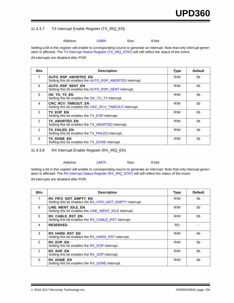
UPD360
11.4.3.7 TX Interrupt Enable Register (TX_IRQ_EN)
Setting a bit in this register will enable to corresponding source to generate an interrupt. Note that only interrupt gener-ation is affected. The TX Interrupt Status Register (TX_IRQ_STAT) will still reflect the status of the event.
All interrupts are disabled after POR.
11.4.3.8 RX Interrupt Enable Register (RX_IRQ_EN)
Setting a bit in this register will enable to corresponding source to generate an interrupt. Note that only interrupt gener-ation is affected. The RX Interrupt Status Register (RX_IRQ_STAT) will still reflect the status of the event.
All interrupts are disabled after POR.
Address: 1A86h Size: 8 bits
Bits Description Type Default
7 AUTO_RSP_ABORTED_ENSetting this bit enables the AUTO_RSP_ABORTED interrupt.
R/W 0b
6 AUTO_RSP_SENT_ENSetting this bit enables the AUTO_RSP_SENT interrupt.
R/W 0b
5 OK_TO_TX_ENSetting this bit enables the OK_TO_TX interrupt.
R/W 0b
4 CRC_RCV_TIMEOUT_ENSetting this bit enables the CRC_RCV_TIMEOUT interrupt.
R/W 0b
3 TX_EOP_ENSetting this bit enables the TX_EOP interrupt.
R/W 0b
2 TX_ABORTED_ENSetting this bit enables the TX_ABORTED interrupt.
R/W 0b
1 TX_FAILED_ENSetting this bit enables the TX_FAILED interrupt.
R/W 0b
0 TX_DONE_ENSetting this bit enables the TX_DONE interrupt.
R/W 0b
Address: 1A87h Size: 8 bits
Bits Description Type Default
7 RX_FIFO_NOT_EMPTY_ENSetting this bit enables the RX_FIFO_NOT_EMPTY interrupt.
R/W 0b
6 LINE_WENT_IDLE_ENSetting this bit enables the LINE_WENT_IDLE interrupt.
R/W 0b
5 RX_CABLE_RST_ENSetting this bit enables the RX_CABLE_RST interrupt.
R/W 0b
4 RESERVED RO -
3 RX_HARD_RST_ENSetting this bit enables the RX_HARD_RST interrupt.
R/W 0b
2 RX_EOP_ENSetting this bit enables the RX_EOP interrupt.
R/W 0b
1 RX_SOP_ENSetting this bit enables the RX_SOP interrupt.
R/W 0b
0 RX_DONE_ENSetting this bit enables the RX_DONE interrupt.
R/W 0b
2016-2017 Microchip Technology Inc. DS00002084C-page 159

UPD360
11.4.3.9 RX Error Interrupt Enable Register (RX_ERR_IRQ_EN)
Setting a bit in this register will enable to corresponding source to generate an interrupt. Note that only interrupt gener-ation is affected. The RX Error Interrupt Status Register (RX_ERR_IRQ_STAT) will still reflect the status of the event.
All interrupts are disabled after POR.
11.4.3.10 Power Management Interrupt Enable and Control Register (PM_IRQ_EN)
Setting a bit in this register will enable to corresponding source to generate an interrupt. Note that only interrupt gener-ation is affected. The Power Management Interrupt Status Register (PM_IRQ_STAT) will still reflect the status of theevent.
All interrupts are disabled after POR. This register also enables clock start and stop requests.
Address: 1A88h Size: 8 bits
Bits Description Type Default
7 DBG_EVENT_ENSetting this bit enables the DBG_EVENT interrupt.
R/W 0b
6:4 RESERVED RO -
3 RX_BAD_PKT_ENSetting this bit enables the RX_BAD_PKT interrupt.
R/W 0b
2 RX_BUF_OVR_RUN_ENSetting this bit enables the RX_BUF_OVR_RUN interrupt.
R/W 0b
1 RX_PCOL_ERROR_ENSetting this bit enables the RX_PCOL_ERROR interrupt.
R/W 0b
0 RX_PKT_DROPPED_ENSetting this bit enables the RX_PKT_DROPPED interrupt.
R/W 0b
Address: 1A89h Size: 8 bits
Bits Description Type Default
7:4 RESERVED RO -
3 UPD_CLK_STOP_ENIf this bit is set, the MAC, upon going idle, will request that the system clock be stopped.
If this bit is cleared, software is responsible to return the device to sleep mode.
This bit does not affect the wake up interrupt (UPD_ACT_WS) generation.
Note: This bit does not affect the MAC's indication that it requires theclock. Even if this bit is cleared, the MAC, once it is idle, will indi-cate that it does not need the clock.
R/W 0b
DS00002084C-page 160 2016-2017 Microchip Technology Inc.

UPD360
11.4.3.11 RX SOP Interrupt Enable Register (RX_SOP_IRQ_EN)
Setting a bit in this register will enable to corresponding source to generate an interrupt. Note that only interrupt gener-ation is affected. The RX SOP Interrupt Status Register (RX_SOP_IRQ_STAT) will still reflect the status of the event.
All interrupts are disabled after POR.
2 UPD_WU_ENIf this bit is set, the MAC, upon detecting receive activity, will request that the system clock be started.
This bit does not affect the wake up interrupt (UPD_ACT_WS) generation.
Note: Once clocks have been started, this bit does not affect the MAC'sindication that it requires the clock. Even if this bit is cleared, theMAC, once it is non-idle (i.e. squelch is active), will indicate that itrequires the clock. Only the period between the asynchronouswake up and the start of squelch is affected.
R/W 0b
1 RESERVED RO -
0 USB_PD_ACT_WS_ENSetting this bit enables the UPD_ACT_WS interrupt.
R/W 0b
Address: 1A8Ah Size: 8 bits
Bits Description Type Default
7:5 RESERVED RO -
4:0 RX_SOP_ENSetting a bit enables the corresponding RX_SOP interrupt.Bit 0: SOPBit 1: SOP'Bit 2: SOP''Bit 3: SOP'_DebugBit 4: SOP''_Debug
R/W 00000b
Bits Description Type Default
2016-2017 Microchip Technology Inc. DS00002084C-page 161
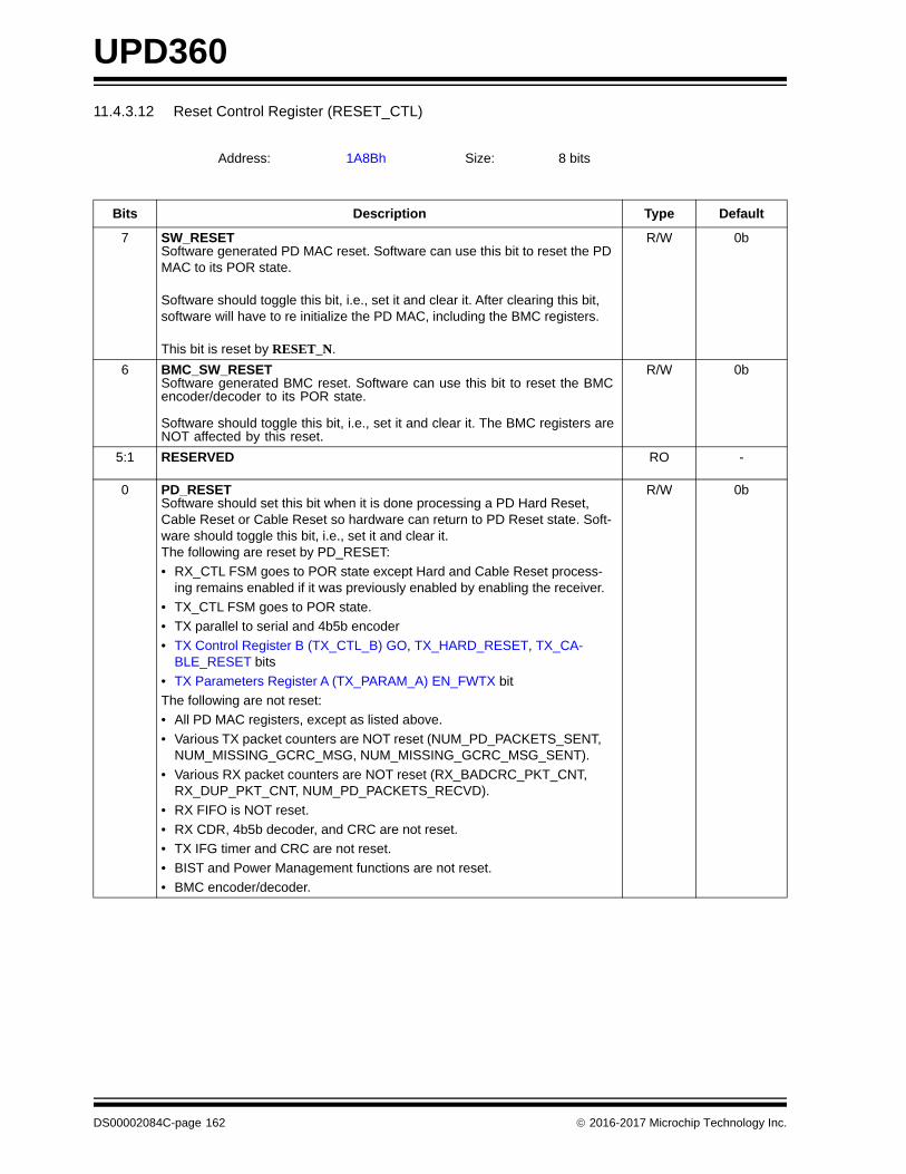
UPD360
11.4.3.12 Reset Control Register (RESET_CTL)
Address: 1A8Bh Size: 8 bits
Bits Description Type Default
7 SW_RESETSoftware generated PD MAC reset. Software can use this bit to reset the PD MAC to its POR state.
Software should toggle this bit, i.e., set it and clear it. After clearing this bit, software will have to re initialize the PD MAC, including the BMC registers.
This bit is reset by RESET_N.
R/W 0b
6 BMC_SW_RESETSoftware generated BMC reset. Software can use this bit to reset the BMC encoder/decoder to its POR state.
Software should toggle this bit, i.e., set it and clear it. The BMC registers are NOT affected by this reset.
R/W 0b
5:1 RESERVED RO -
0 PD_RESETSoftware should set this bit when it is done processing a PD Hard Reset, Cable Reset or Cable Reset so hardware can return to PD Reset state. Soft-ware should toggle this bit, i.e., set it and clear it.The following are reset by PD_RESET:
• RX_CTL FSM goes to POR state except Hard and Cable Reset process-ing remains enabled if it was previously enabled by enabling the receiver.
• TX_CTL FSM goes to POR state.
• TX parallel to serial and 4b5b encoder
• TX Control Register B (TX_CTL_B) GO, TX_HARD_RESET, TX_CA-BLE_RESET bits
• TX Parameters Register A (TX_PARAM_A) EN_FWTX bit
The following are not reset:
• All PD MAC registers, except as listed above.
• Various TX packet counters are NOT reset (NUM_PD_PACKETS_SENT, NUM_MISSING_GCRC_MSG, NUM_MISSING_GCRC_MSG_SENT).
• Various RX packet counters are NOT reset (RX_BADCRC_PKT_CNT, RX_DUP_PKT_CNT, NUM_PD_PACKETS_RECVD).
• RX FIFO is NOT reset.
• RX CDR, 4b5b decoder, and CRC are not reset.
• TX IFG timer and CRC are not reset.
• BIST and Power Management functions are not reset.
• BMC encoder/decoder.
R/W 0b
DS00002084C-page 162 2016-2017 Microchip Technology Inc.
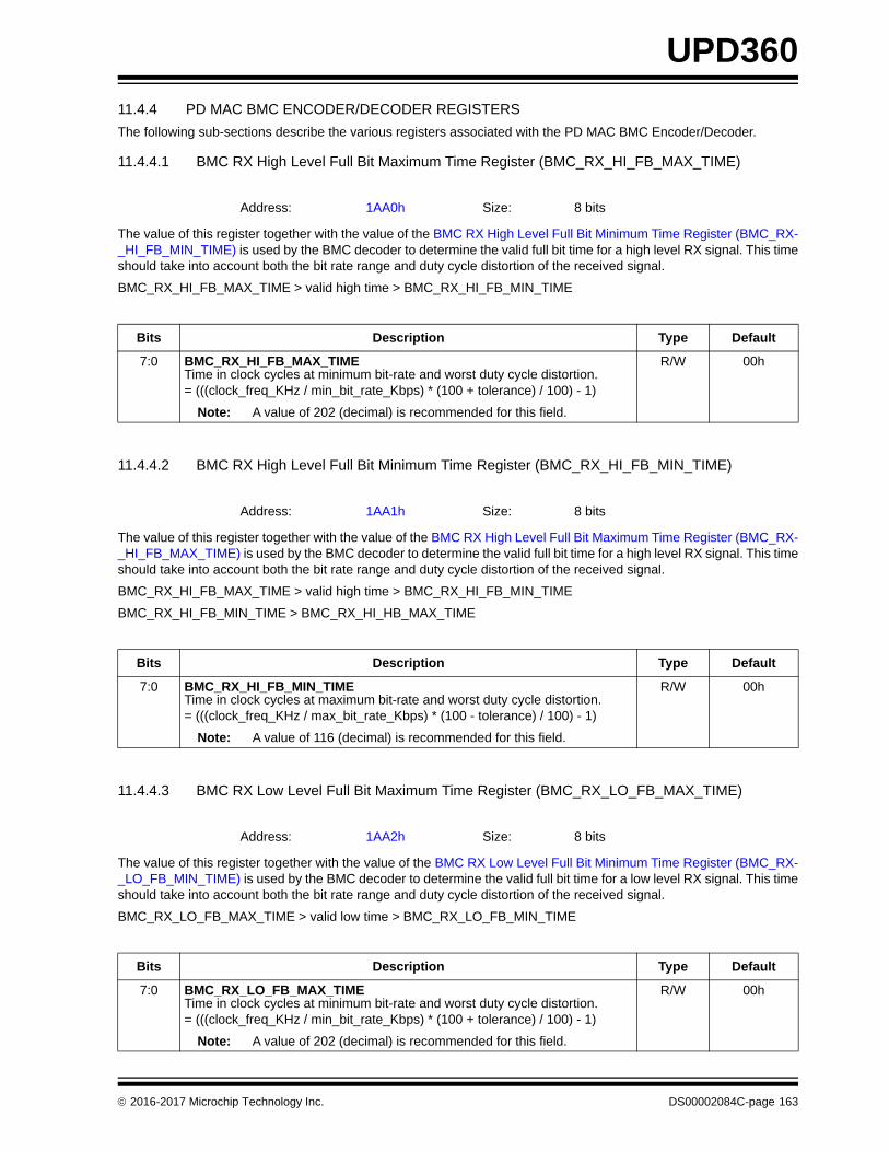
UPD360
11.4.4 PD MAC BMC ENCODER/DECODER REGISTERS
The following sub-sections describe the various registers associated with the PD MAC BMC Encoder/Decoder.
11.4.4.1 BMC RX High Level Full Bit Maximum Time Register (BMC_RX_HI_FB_MAX_TIME)
The value of this register together with the value of the BMC RX High Level Full Bit Minimum Time Register (BMC_RX-_HI_FB_MIN_TIME) is used by the BMC decoder to determine the valid full bit time for a high level RX signal. This timeshould take into account both the bit rate range and duty cycle distortion of the received signal.
BMC_RX_HI_FB_MAX_TIME > valid high time > BMC_RX_HI_FB_MIN_TIME
11.4.4.2 BMC RX High Level Full Bit Minimum Time Register (BMC_RX_HI_FB_MIN_TIME)
The value of this register together with the value of the BMC RX High Level Full Bit Maximum Time Register (BMC_RX-_HI_FB_MAX_TIME) is used by the BMC decoder to determine the valid full bit time for a high level RX signal. This timeshould take into account both the bit rate range and duty cycle distortion of the received signal.
BMC_RX_HI_FB_MAX_TIME > valid high time > BMC_RX_HI_FB_MIN_TIME
BMC_RX_HI_FB_MIN_TIME > BMC_RX_HI_HB_MAX_TIME
11.4.4.3 BMC RX Low Level Full Bit Maximum Time Register (BMC_RX_LO_FB_MAX_TIME)
The value of this register together with the value of the BMC RX Low Level Full Bit Minimum Time Register (BMC_RX-_LO_FB_MIN_TIME) is used by the BMC decoder to determine the valid full bit time for a low level RX signal. This timeshould take into account both the bit rate range and duty cycle distortion of the received signal.
BMC_RX_LO_FB_MAX_TIME > valid low time > BMC_RX_LO_FB_MIN_TIME
Address: 1AA0h Size: 8 bits
Bits Description Type Default
7:0 BMC_RX_HI_FB_MAX_TIMETime in clock cycles at minimum bit-rate and worst duty cycle distortion.= (((clock_freq_KHz / min_bit_rate_Kbps) * (100 + tolerance) / 100) - 1)
Note: A value of 202 (decimal) is recommended for this field.
R/W 00h
Address: 1AA1h Size: 8 bits
Bits Description Type Default
7:0 BMC_RX_HI_FB_MIN_TIMETime in clock cycles at maximum bit-rate and worst duty cycle distortion.= (((clock_freq_KHz / max_bit_rate_Kbps) * (100 - tolerance) / 100) - 1)
Note: A value of 116 (decimal) is recommended for this field.
R/W 00h
Address: 1AA2h Size: 8 bits
Bits Description Type Default
7:0 BMC_RX_LO_FB_MAX_TIMETime in clock cycles at minimum bit-rate and worst duty cycle distortion.= (((clock_freq_KHz / min_bit_rate_Kbps) * (100 + tolerance) / 100) - 1)
Note: A value of 202 (decimal) is recommended for this field.
R/W 00h
2016-2017 Microchip Technology Inc. DS00002084C-page 163
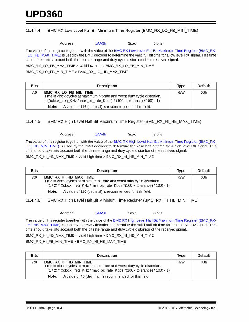
UPD360
11.4.4.4 BMC RX Low Level Full Bit Minimum Time Register (BMC_RX_LO_FB_MIN_TIME)
The value of this register together with the value of the BMC RX Low Level Full Bit Maximum Time Register (BMC_RX-_LO_FB_MAX_TIME) is used by the BMC decoder to determine the valid full bit time for a low level RX signal. This timeshould take into account both the bit rate range and duty cycle distortion of the received signal.
BMC_RX_LO_FB_MAX_TIME > valid low time > BMC_RX_LO_FB_MIN_TIME
BMC_RX_LO_FB_MIN_TIME > BMC_RX_LO_HB_MAX_TIME
11.4.4.5 BMC RX High Level Half Bit Maximum Time Register (BMC_RX_HI_HB_MAX_TIME)
The value of this register together with the value of the BMC RX High Level Half Bit Minimum Time Register (BMC_RX-_HI_HB_MIN_TIME) is used by the BMC decoder to determine the valid half bit time for a high level RX signal. Thistime should take into account both the bit rate range and duty cycle distortion of the received signal.
BMC_RX_HI_HB_MAX_TIME > valid high time > BMC_RX_HI_HB_MIN_TIME
11.4.4.6 BMC RX High Level Half Bit Minimum Time Register (BMC_RX_HI_HB_MIN_TIME)
The value of this register together with the value of the BMC RX High Level Half Bit Maximum Time Register (BMC_RX-_HI_HB_MAX_TIME) is used by the BMC decoder to determine the valid half bit-time for a high level RX signal. Thistime should take into account both the bit rate range and duty cycle distortion of the received signal.
BMC_RX_HI_HB_MAX_TIME > valid high time > BMC_RX_HI_HB_MIN_TIME
BMC_RX_HI_FB_MIN_TIME > BMC_RX_HI_HB_MAX_TIME
Address: 1AA3h Size: 8 bits
Bits Description Type Default
7:0 BMC_RX_LO_FB_MIN_TIMETime in clock cycles at maximum bit-rate and worst duty cycle distortion.= (((clock_freq_KHz / max_bit_rate_Kbps) * (100 - tolerance) / 100) - 1)
Note: A value of 116 (decimal) is recommended for this field.
R/W 00h
Address: 1AA4h Size: 8 bits
Bits Description Type Default
7:0 BMC_RX_HI_HB_MAX_TIMETime in clock cycles at minimum bit-rate and worst duty cycle distortion.=((1 / 2) * ((clock_freq_KHz / min_bit_rate_Kbps)*(100 + tolerance) / 100) - 1)
Note: A value of 110 (decimal) is recommended for this field.
R/W 00h
Address: 1AA5h Size: 8 bits
Bits Description Type Default
7:0 BMC_RX_HI_HB_MIN_TIMETime in clock cycles at maximum bit-rate and worst duty cycle distortion.=((1 / 2) * ((clock_freq_KHz / max_bit_rate_Kbps)*(100 - tolerance) / 100) - 1)
Note: A value of 48 (decimal) is recommended for this field.
R/W 00h
DS00002084C-page 164 2016-2017 Microchip Technology Inc.
UPD360
11.4.4.7 BMC RX Low Level Half Bit Maximum Time Register (BMC_RX_LO_HB_MAX_TIME)
The value of this register together with the value of the BMC RX Low Level Half Bit Minimum Time Register (BMC_RX-_LO_HB_MIN_TIME) is used by the BMC decoder to determine the valid half bit-time for a low level RX signal. Thistime should take into account both the bit rate range and duty cycle distortion of the received signal.
BMC_RX_LO_HB_MAX_TIME > valid low time > BMC_RX_LO_HB_MIN_TIME
11.4.4.8 BMC RX Low Level Half Bit Minimum Time Register (BMC_RX_LO_HB_MIN_TIME)
The value of this register together with the value of the BMC RX Low Level Half Bit Maximum Time Register (BMC_RX-_LO_HB_MAX_TIME) is used by the BMC decoder to determine the valid half bit-time for a low level RX signal. Thistime should take into account both the bit rate range and duty cycle distortion of the received signal.
BMC_RX_LO_HB_MAX_TIME > valid low time > BMC_RX_LO_HB_MIN_TIME
BMC_RX_LO_FB_MIN_TIME > BMC_RX_LO_HB_MAX_TIME
Address: 1AA6h Size: 8 bits
Bits Description Type Default
7:0 BMC_RX_LO_HB_MAX_TIMETime in clock cycles at minimum bit-rate and worst duty cycle distortion.=((1 / 2) * ((clock_freq_KHz / min_bit_rate_Kbps)*(100 + tolerance) / 100) - 1)
Note: A value of 110 (decimal) is recommended for this field.
R/W 00h
Address: 1AA7h Size: 8 bits
Bits Description Type Default
7:0 BMC_RX_LO_HB_MIN_TIMETime in clock cycles at maximum bit-rate and worst duty cycle distortion.=((1 / 2) * ((clock_freq_KHz / max_bit_rate_Kbps)*(100 - tolerance) / 100) - 1)
Note: A value of 48 (decimal) is recommended for this field.
R/W 00h
2016-2017 Microchip Technology Inc. DS00002084C-page 165

UPD360
11.4.4.9 BMC RX Squelch Assert Time Register (BMC_RX_SQL_ASSERT_TIME)
The value of this register is used by the BMC decoder to determine when there is a valid signal. If three edges of thereceive signal are seen within this time, then the “squelch” goes active. This time should take into account the minimumbit rate but does not need to account for the duty cycle distortion of the received signal.
11.4.4.10 BMC RX Squelch Hold Time Register (BMC_RX_SQL_HOLD_TIME)
The value of this register is used by the BMC decoder to provide time for the CDR circuit to output the final bit of data.A typical hold time would be 1 maximum half bit time pulse desired tolerance.
Address: 1AA8h Size: 8 bits
Bits Description Type Default
7:0 BMC_RX_SQL_ASSERT_TIMETime in clock cycles x 4 at minimum bit-rate.
assert time uS = (BMC_RX_SQL_ASSERT_TIME x 4 + 1) / clock_freq MHz
A typical assert time would be 3 maximum half bit times plus desired toler-ance.
Note: A value of 70 (decimal) is recommended for this field.
R/W 00h
Address: 1AA9h Size: 8 bits
Note: The Squelch Drop time is based on the BMC RX Maximum High and Low Time registers.
Bits Description Type Default
7:0 BMC_RX_SQL_HOLD_TIMETime in clock cycles x 4 at minimum bit-rate.
hold time uS = (BMC_RX_SQL_HOLD_TIME x 4 + 1) / clock_freq MHz
typical value = ((1 / 2) * ((clock_freq_KHz / min_bit_rate_Kbps) * (100 + tolerance) / 100) - 1) / 4
Note: A value of 23 (decimal) is recommended for this field.
R/W 00h
DS00002084C-page 166 2016-2017 Microchip Technology Inc.
UPD360
11.4.4.11 BMC TX Bit-Time Count Register (BMC_TX_BITTIME_CNT)
11.4.4.12 BMC Transition Window Time Register (BMC_TRANSITION_WINDOW_TIME)
The value of this register is used by the BMC decoder to determine when the line is IDLE. Detection is active when 3transitions occur at the receiver within a time window of BMC_TRANSITION_WINDOW_TIME. After waitingBMC_TRANSITION_WINDOW_TIME without detecting 3 transitions, the bus is considered idle. The USB PD Specifi-cation calls for 12uS minimum and 20uS maximum.
Address: 1AB0h Size: 8 bits
Bits Description Type Default
7:0 BMC_TX_BIT_TIME_CNTBit-time counter value. The BMC encoder uses this value to determine the bit-timing for the last bit of data. This register can be used to adjust bit-time for testing purpose (adjusting bitrate).
Count value is based on clock frequency and is given by:((Clock Freq KHz / Bit Rate Kbps) - 1)i.e.,Clock Frequency = 48000KHz (48MHz)Nominal Bit Rate = 300 Kbpsbit_time_cnt = (48000 / 300) - 1 = 159
Note: A value of 159 (decimal) is recommended for this field.
R/W 00h
Address: 1AB1h Size: 8 bits
Bits Description Type Default
7:0 BMC_TRANSITION_WINDOW_TIMETime in clock cycles x 4
transition time uS = (BMC_TRANSITION WINDOW_TIME x 4) / clock_freq MHz
Per the USB PD Specification, this value should be set between 12uS and 20uS. This would be a value between 144 and 240 at 48MHz.
Note: Unlike the TX Turnaround Time Register (TX_TA_TIME), this hard-ware does not use a pre-scaler, therefore the time specified isaccurate.
Note: A value of 200 (decimal) is recommended for this field.
R/W 00h
2016-2017 Microchip Technology Inc. DS00002084C-page 167
UPD360
11.4.5 PD MAC BIST REGISTERS
The following sub-sections describe the various registers associated with the PD MAC Built-In Self Test (BIST).
11.4.5.1 BIST Control Register A (BIST_CTL_A)
Address: 1AC0h Size: 8 bits
Bits Description Type Default
7:5 RESERVED RO -
4 BIST_RX_ENEnable BIST Receiver.
Setting this bit will:
• Enable the BIST receiver.
• Reset the PRBS generator in the BIST RX logic so it is ready to compare incoming BIST PRBS pattern.
• Reset the BIST error count registers (BIST Error Count High Register (BIST_ERR_CNT_HI) and BIST Error Count Low Register (BIST_ER-R_CNT_LO).
Normally this bit is set only when BIST receiver mode is required; however, this bit can be set to enable loopback BIST testing by disabling Automatic Response Mode and enabling the RX loopback (setting the EN_LOOPBACK bit in the RX Control Register A (RX_CTL_A)).
This bit must be cleared and set by software every time a new BIST RX request comes in.
Note: In BIST loopback test mode, BIST TX must be manually triggeredfor each TX packet since functional receiver path is disabled.
R/W 0b
3 BIST_ENEnable BIST. Set this bit when BIST logic is activated.This bit together with the EN_LOOPBACK bit in the RX Control Register A (RX_CTL_A) is used by hardware to block received data from going into func-tional path. This means that when loopback is enabled in BIST mode hard-ware cannot detect hard reset.
This bit also powers up the BMC transmitter for BIST mode operation. Soft-ware should set this bit for a sufficient amount of time (5us) before trigger transmission of BIST frame via BIST_TX_START/BIST_TX_STATUS.
R/W 0b
2:0 BIST_TX_MODESet BIST Test Mode. Only the following mode is supported:010b: BIST Carrier Test Mode-2 (alternating '1's and '0's)
All other modes are reserved and should not be used.
R/W 000b
DS00002084C-page 168 2016-2017 Microchip Technology Inc.
UPD360
11.4.5.2 BIST Control Register B (BIST_CTL_B)
Address: 1AC1h Size: 8 bits
Bits Description Type Default
7:3 RESERVED RO -
2 BIST_CLR_ERR_CNTClears the BIST error count registers BIST Error Count High Register (BIST_ERR_CNT_HI) and BIST Error Count Low Register (BIST_ER-R_CNT_LO).
WO 0b
1 BIST_TX_RSTReset the TX logic and PRBS generator. Software must set this bit once before starting the BIST test, i.e., setting BIST_TX_START/BIST_TX_STA-TUS bit for the first time.
Since this bit resets the PRBS generator it should not be set again until the current BIST test is ended.
This bit is not latched and will always read '0'
The PRBS generator cannot be reset by BIST_TX_START/BIST_TX_STA-TUS because that would reset it for each TX BIST frame.This bit should be used to stop the continuous BIST TX mode (2). It may take up to 1 bit time for the TX to stop. BIST_EN should not be cleared until after this time.
Note: If this bit is set simultaneously with BIST_TX_START/BIST_TX-_STATUS, it takes precedence and will void BIST_TX_START/BIST_TX_STATUS.
WO 0b
0 BIST_TX_START/BIST_TX_STATUSStart BIST transmission. Setting this bit will trigger transmission of BIST frame.
This bit is not latched and reading it will return the status of current BIST transmission.
Depending on BIST Mode, transmission will either continue indefinitely (unless BIST_TX_RST is asserted) or stop after sending a BIST PRBS frame.
BIST does not support sending of next BIST frame automatically. It must be triggered by software by first clearing and then re-setting this bit.
Note: This bit cannot be set simultaneously with BIST_TX_RST.BIST_TX_RST has precedence and will void BIST_TX_START/BIST_TX_STATUS.
In BIST RX mode, hardware will automatically send the BIST Error Count message if the EN_AUTO_RSP_MODE bit in the TX Control Register A (TX_CTL_A) is set.
WO/RO 0b
2016-2017 Microchip Technology Inc. DS00002084C-page 169
UPD360
11.4.5.3 BIST Error Count High Register (BIST_ERR_CNT_HI)
11.4.5.4 BIST Error Count Low Register (BIST_ERR_CNT_LO)
11.4.5.5 BIST RX Status Register (BIST_RX_STAT)
This register is used to help with functional testing. Hardware is configured to transmit BIST PRBS frames. At the sametime, loopback mode is enabled and BIST receive mode is enabled. Now when a PRBS frame is transmitted it is alsoreceived and compared. This register provides information when the BIST PRBS frame is done receiving and whetherthere were any errors detected.
Address: 1AC2h Size: 8 bits
Bits Description Type Default
7:0 BIST_ERR_CNT_HI[7:0]Upper byte of BIST error count (bits 15-8) (BIST_ERR_CNT[15:8])
RO 00h
Address: 1AC3h Size: 8 bits
Bits Description Type Default
7:0 BIST_ERR_CNT_LO[7:0]Lower byte of BIST error count (bits 7-0) (BIST_ERR_CNT[7:0])
RO 00h
Address: 1AC7h Size: 8 bits
Bits Description Type Default
7:2 RESERVED RO -
1 BIST_RX_ERRORThis bit is valid only when BIST_RX_DONE bit is set.
A value of “0” indicates that BIST PRBS frame was received without errors.A value of “1” indicates that BIST PRBS frame was received with errors.
RO 0b
0 BIST_RX_DONESuccessfully received a BIST RX FRAME.Writing a “1” to this bit will clear it.
R/W1C 0b
DS00002084C-page 170 2016-2017 Microchip Technology Inc.
UPD360
12.0 USB PORT POWER CONTROLLER (PPC)
The device’s USB Port Power Controller (PPC) provides 3.0 A of continuous current (3.2 A max) on VBUS with precisionover-current limiting (OCL), under- and over-voltage lockout, and dynamic thermal management. The PPC also includesa VBUS discharge function and constant current mode current limiting for BC 1.2 applications.
12.1 PPC Power States
The PPC provides the following power states:
• Sleep: This is the lowest PPC power state available. See Section 12.1.1, "Sleep State Operation" for additional information.
• Error: This state is entered when a fault condition exists. The PPC interrupt status registers detail the error condi-tion. See Section 12.1.3, "Error State Operation" for additional information.
• Active: In this state, the PPC is active and sourcing current to VBUS. No errors are present. This power state pro-vides full functionality. While in this state, operations include activation of the port power switch and current limit-ing. See Section 12.1.2, "Active State Operation" for additional information.
12.1.1 SLEEP STATE OPERATION
The PWR_EN pin (UPD360-A/UPD360-B operating in standalone DFP mode only) may be used to cause the PPC toenter/exit sleep. When the PPC is in the Sleep state, the device will be in its lowest power state. The bypass switch, andthe port power switch will be disabled. VBUS will be near ground potential.
12.1.2 ACTIVE STATE OPERATION
When the PPC enters the Active state, the port power switch is closed. The PPC cannot be in the Active state (andtherefore, the port power switch cannot be turned on) if any of the following conditions exist:
• VS < VS_UVLO (2.5 V).
• PWR_EN is disabled (standalone DFP mode only).
12.1.3 ERROR STATE OPERATION
The PPC will enter the Error state from the Active state when any of the following events are detected:
• The maximum allowable internal die temperature tTSD has been exceeded.
• An over-current condition has been detected.
• An under-voltage condition on VS has been detected (see Section 12.2.1, "Under-Voltage Lockout on VS").
• A discharge error has been detected.
• An over-voltage condition on the VS pin.
When the PPC enters the Error state, the port power switch and the VBUS bypass switch will be disabled, and ALERTis asserted (by default). They will remain off while in this power state. The PPC will leave this state as determined bythe fault handling selection.
With the Auto-recovery fault handler, the PPC will check that all of the error conditions have been removed. If all of theerror conditions have been removed, the PPC will return to the Active state. The ERR_RECOVER pin is used in stand-alone DFP mode to select the auto-recovery algorithm.
12.2 Supply Voltages
12.2.1 UNDER-VOLTAGE LOCKOUT ON VS
The PPC requires a minimum voltage VS_UVLO (2.5 V) be present on the VS pin for the Active power state.
Note: The PPC DC and AC parameters can be seen in Table 16-6, “Port Power Controller DC Parameters,” onpage 209 and Table 16-12, “Port Power Controller AC Parameters,” on page 212, respectively.
Note: The PPC power state is reflected in the PWR_STATE[1:0] field of the PPC General Configuration 3 Reg-ister (PPC_GENERAL_CFG3).
2016-2017 Microchip Technology Inc. DS00002084C-page 171
UPD360
12.2.2 OVER-VOLTAGE DETECTION LOCKOUT ON VS
The port power switch will be disabled if the voltage on the VS pin exceeds a voltage VS_OV for longer than the specifiedtime tMASK (5 ms). This will cause the device to enter the Error state.
12.2.3 PWR_EN INPUT (UPD360-A/UPD360-B ONLY)
In standalone DFP mode, the PWR_EN pin enables the port power switch to be turned on if conditions are met. Theport power switch cannot be closed if PWR_EN is disabled. However, if PWR_EN is enabled, the port power switch isnot necessarily closed (see Section 12.1.2, "Active State Operation"). The PWR_EN pin state will be ignored by the PPCif the PIN_IGNORE configuration bit is set. Otherwise, the PWR_EN_SET configuration bit is checked along with thePWR_EN pin.
12.3 USB Port Power Switch
To assure compliance to USB Type-CTM, the PPC contains a USB port power switch that supports trip current limitingmode.
The current limit (ILIM) is set via the PWR_CAP0 and PWR_CAP1 pins (UPD360-A/UPD360-B only), and may also beupdated via the PPC Current Limit Register (PPC_CURRENT_LIMIT). The switch also includes soft start circuitry anda separate short circuit current limit. The port power switch is on in the Active state (except when VBUS is discharging).
12.3.1 CURRENT LIMITING
The current limit (ILIM) is set via the PWR_CAP0 and PWR_CAP1 pins (UPD360-A/UPD360-B only). These pins areread at device power-up. The current limit can be changed via the PPC Current Limit Register (PPC_CURRENT_LIMIT)after power-up. However, the programmed current limit cannot exceed the hardware set current limit defined by thePWR_CAP0 and PWR_CAP1 pins.
The UPD360 is pre-configured with appropriate settings to satisfy the USB Type-C™ current limiting requirements andno register writes are necessary to use this internal 5V port power controller, when operating in standalone mode.
12.3.1.1 Short Circuit Output Current Limiting
Short circuit current limiting occurs when the output current is above the selectable current limit (PPC Current Limit Reg-ister (PPC_CURRENT_LIMIT)). This event will be detected and the current will immediately be limited within thetSHORT_LIM time. If the condition remains, the port power switch will flag an Error condition and enter the Error state.
12.3.1.2 Soft Start
When the PWR_EN control (UPD360-A/UPD360-B only) changes states to enable the port power switch, the PPCinvokes a soft start routine for the duration of the VBUS rise time (tR_BUS). This soft start routine will limit current flowfrom VS into VBUS while it is active. This circuitry will prevent current spikes due to a step in the portable device currentdraw.
In the case when a portable device is attached while the PWR_EN pin is already enabled (in standalone DFP mode), orthe PWR_EN_SET bit is enabled, if the bus current exceeds ILIM, the PPC current limiter will respond within a specifiedtime (tSHORT_LIM) and will operate normally at this point. The CBUS capacitor will deliver the extra current, if any, asrequired by the load change.
12.3.1.3 Current Limiting Modes
The PPC current limiting operates in trip mode. This mode is active when the port power switch is closed. When oper-ating in the Detect power state, the current capacity at VBUS is limited to IBUS_BYP”.
12.3.1.3.1 Trip Mode
When using trip current limiting, the PPC USB port power switch functions as a low resistance switch and rapidly turnsoff if the current limit is exceeded. While operating using trip current limiting, the VBUS output voltage will be held rela-tively constant (equal to the VS voltage minus the RON_PSW * IBUS current) for all current values up to the ILIM. If theinternal temperature exceeds tTSD threshold, the port power switch will open.
If the current drawn by a portable device exceeds ILIM, the following occurs:
Note: If a load that draws between 2 mA and 7 mA is connected to the port power switch, a voltage ripple between40-90 mVPP is observed at the VBUS output. This behavior is normal and it does not affect the chargingprocess when a portable device is connected.
DS00002084C-page 172 2016-2017 Microchip Technology Inc.
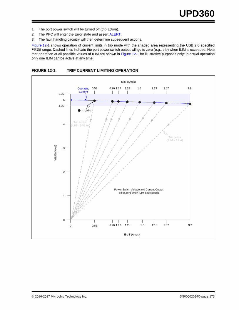
UPD360
1. The port power switch will be turned off (trip action).
2. The PPC will enter the Error state and assert ALERT.
3. The fault handling circuitry will then determine subsequent actions.
Figure 12-1 shows operation of current limits in trip mode with the shaded area representing the USB 2.0 specifiedVBUS range. Dashed lines indicate the port power switch output will go to zero (e.g., trip) when ILIM is exceeded. Notethat operation at all possible values of ILIM are shown in Figure 12-1 for illustrative purposes only; in actual operationonly one ILIM can be active at any time.
FIGURE 12-1: TRIP CURRENT LIMITING OPERATION
5
4
3
2
1
0.53 1.07 1.6 2.67 3.2
5.25
4.75
IBUS (Amps)
VB
US
(V
olts
)
Operating Current
0
0
0.96 1.28
1.281.070.960.53 1.6 3.22.13 2.67
= ILIM’s
2.13
Power Switch Voltage and Current Output go to Zero when ILIM is Exceeded
Trip action (ILIM = 0.53 A)
Trip action (ILIM = 3.2 A)
ILIM (Amps)
2016-2017 Microchip Technology Inc. DS00002084C-page 173

UPD360
Figure 12-2 illustrates the relationship between these USB port power profile parameters.
FIGURE 12-2: PORT POWER PROFILE PARAMETERS EXAMPLE
5
4
3
2
1
0.53 1.6 2.67 3.2
5.25
4.75
0
0
Port Power Profile Operating Region
0.96 1.28
1.280.960.53 1.6
IBUS_R2MIN
2.13
2.13 2.67 3.2
IBUS (Amps)
VB
US
(V
olts
)
ILIM (Amps)
VBUS_MIN
Enforced KEEP-OUT
KEEP-OUT
DS00002084C-page 174 2016-2017 Microchip Technology Inc.

UPD360
12.3.2 THERMAL MANAGEMENT
The PPC utilizes internal thermal management:
12.3.2.1 Thermal Shutdown
The thermal management consists of a hardware implemented thermal shutdown corresponding to the maximum allow-able internal die temperature (tTSD). If the internal temperature exceeds this value, the port power switches (both ports)will immediately be turned off until the temperature is below tTSD - tTSD_HYST.
12.3.3 VBUS DISCHARGE
The PPC will discharge VBUS through an internal 100 Ohm resistor when at least one of the following conditions occurs:
• The PWR_EN control (UPD360-A/UPD360-B only) is disabled (triggered on the inactive edge of the PWR_EN control) (Standalone DFP mode only).
• The VS voltage drops below a specified threshold VS_UVLO (2.5 V) that causes the port power switch to be dis-abled.
• When commanded into the Sleep power state.
• Upon recovery from the Error state.
• When commanded via the DISCHARGE bit.
• Any time that the port power switch is activated after the VBUS bypass switch has been on.
• Any time that the VBUS bypass switch is activated after the port power switch has been on.
When the VBUS discharge circuitry is activated, at the end of the tDISCHARGE time, the PPC will confirm that VBUS wasdischarged. If the VBUS voltage is not below the VTEST level, a discharge error will be flagged (by setting theVBUS Dis-charge Error bit in the Power Interrupt Status Register (PWR_INT_STS)) and the PPC will enter the Error state.
12.4 VBUS Bypass Switch
The device contains circuitry to provide VBUS current as shown in Figure 12-3. The VBUS bypass switch and the portpower switch are never both on at the same time.
FIGURE 12-3: VBUS BYPASS SWITCH
Port Power Switch
VS
VS VBUS
VBUS
Bypass Switch
2016-2017 Microchip Technology Inc. DS00002084C-page 175
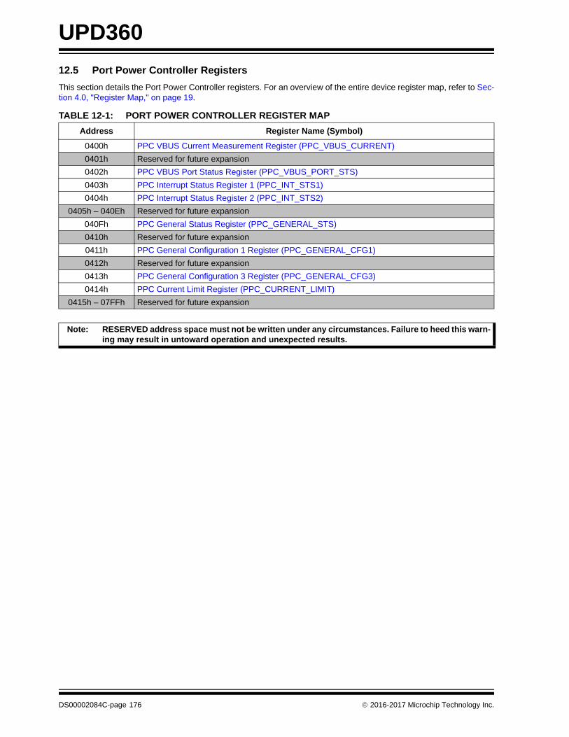
UPD360
12.5 Port Power Controller Registers
This section details the Port Power Controller registers. For an overview of the entire device register map, refer to Sec-tion 4.0, "Register Map," on page 19.
TABLE 12-1: PORT POWER CONTROLLER REGISTER MAP
Address Register Name (Symbol)
0400h PPC VBUS Current Measurement Register (PPC_VBUS_CURRENT)
0401h Reserved for future expansion
0402h PPC VBUS Port Status Register (PPC_VBUS_PORT_STS)
0403h PPC Interrupt Status Register 1 (PPC_INT_STS1)
0404h PPC Interrupt Status Register 2 (PPC_INT_STS2)
0405h – 040Eh Reserved for future expansion
040Fh PPC General Status Register (PPC_GENERAL_STS)
0410h Reserved for future expansion
0411h PPC General Configuration 1 Register (PPC_GENERAL_CFG1)
0412h Reserved for future expansion
0413h PPC General Configuration 3 Register (PPC_GENERAL_CFG3)
0414h PPC Current Limit Register (PPC_CURRENT_LIMIT)
0415h – 07FFh Reserved for future expansion
Note: RESERVED address space must not be written under any circumstances. Failure to heed this warn-ing may result in untoward operation and unexpected results.
DS00002084C-page 176 2016-2017 Microchip Technology Inc.

UPD360
12.5.1 PPC VBUS CURRENT MEASUREMENT REGISTER (PPC_VBUS_CURRENT)
This register stores the measured current value delivered to the external device via the VBUS pin. This value is updatedcontinuously while the device is in the Active power state. The bit weights are in mA and the range is from 0mA to3400mA (1 LSB = 13.3mA).
This data will be cleared whenever the port power switch is turned off (or any time that VBUS is discharged).
Note: This register’s data is not intended for use when current is <100mA.
12.5.2 PPC VBUS PORT STATUS REGISTER (PPC_VBUS_PORT_STS)
Address: 0400h Size: 8 bits
Bits Description Type Default
7 1706.2 mA RO 0b
6 853.1 mA RO 0b
5 426.6 mA RO 0b
4 213.3 mA RO 0b
3 106.6 mA RO 0b
2 53.3 mA RO 0b
1 26.7 mA RO 0b
0 13.3 mA RO 0b
Address: 0402h Size: 8 bits
Bits Description Type Default
7 RESERVED RO -
6 ALERTThis bit is asserted when an error (ERR) occurs in the PPC. It also asserts the PPC_INT bit in the Interrupt Status Register (INT_STS), if enabled.
This bit can also be configured to assert when the LOW_CUR (portable device is pulling less current and may be finished charging) bit is set and linked via the ALERT_LINK bit. The ALERT bit is de-asserted when all error conditions that may assert it (error condition, and LOW_CUR if linked) have been removed or reset as necessary.
RO 0b
5 RESERVED RO -
4 CC_MODEIndicates that the IBUS current on VBUS has exceeded ILIM and sourcing Region 2.
RO 0b
3:0 RESERVED RO -
2016-2017 Microchip Technology Inc. DS00002084C-page 177
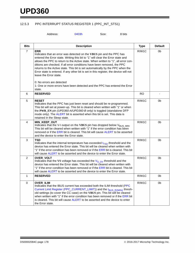
UPD360
12.5.3 PPC INTERRUPT STATUS REGISTER 1 (PPC_INT_STS1)
Address: 0403h Size: 8 bits
Bits Description Type Default
7 ERRIndicates that an error was detected on the VBUS pin and the PPC has entered the Error state. Writing this bit to “1” will clear the Error state and allows the PPC to return to the Active state. When written to “1”, all error con-ditions are checked. If all error conditions have been removed, the PPC returns to the Active state. This bit is set automatically by the PPC when the Error state is entered. If any other bit is set in this register, the device will not leave the Error state.
0: No errors are detected1: One or more errors have been detected and the PPC has entered the Error state.
R/W1C 0b
6 RESERVED RO -
5 RESETIndicates that the PPC has just been reset and should be re-programmed. This bit will set at power-up. This bit is cleared when written with “1” or when the PWR_EN pin (UPD360-A/UPD360-B only) is toggled (standalone DFP mode only). The ALERT bit is asserted when this bit is set. This data is retained in the Sleep state.
R/W1C 0b
4 MIN_KEEP_OUTIndicates that the V-I output on the VBUS pin has dropped below VBUS_MIN. This bit will be cleared when written with “1” if the error condition has been removed or if the ERR bit is cleared. This bit will cause ALERT to be asserted and the device to enter the Error state.
R/W1C 0b
3 TSDIndicates that the internal temperature has exceeded tTSD threshold and the device has entered the Error state. This bit will be cleared when written with “1” if the error condition has been removed or if the ERR bit is cleared. This bit will cause ALERT to be asserted and the device to enter the Error state.
R/W1C 0b
2 OVER_VOLTIndicates that the VS voltage has exceeded the VS_OV threshold and the device has entered the Error state. This bit will be cleared when written with “1” if the error condition has been removed or if the ERR bit is cleared. This bit will cause ALERT to be asserted and the device to enter the Error state.
R/W1C 0b
1 RESERVED R/W1C 0b
0 OVER_ILIMIndicates that the IBUS current has exceeded both the ILIM threshold (PPC Current Limit Register (PPC_CURRENT_LIMIT)) and the IBUS_R2MIN1 thresh-old settings (to cover the CC case) on the VBUS pin. This bit will be cleared when written with “1” if the error condition has been removed or if the ERR bit is cleared. This bit will cause ALERT to be asserted and the device to enter the Error state.
R/W1C 0b
DS00002084C-page 178 2016-2017 Microchip Technology Inc.

UPD360
12.5.4 PPC INTERRUPT STATUS REGISTER 2 (PPC_INT_STS2)
12.5.5 PPC GENERAL STATUS REGISTER (PPC_GENERAL_STS)
Address: 0404h Size: 8 bits
Bits Description Type Default
7:6 RESERVED RO -
5 VS_LOWIndicates that the VS voltage is below the VS_UVLO (2.5 V) threshold and the port power switch is held off. This bit is cleared automatically when the VS voltage is above the VS_UVLO threshold.
R/W1C 0b
4:0 RESERVED RO -
Address: 040Fh Size: 8 bits
Bits Description Type Default
7:5 RESERVED RO -
4 CC_MODEIndicates that the IBUS current has exceeded ILIM (PPC Current Limit Regis-ter (PPC_CURRENT_LIMIT)). This bit identifies that the port power switch current limiting circuitry has been activated and the switch is in current limit mode. This bit will be ‘0’ when the port power switch is off.
R/W1C 0b
3 PWR_ENThis bit reflects the port power switch control state. This bit is set and cleared automatically as the PWR_EN pin (UPD360-A/UPD360-B only) and/or PWR_EN_SET bit state changes.
R/W1C 0b
2 LOW_CURIndicates that a portable device has reduced its charge current to below the threshold on VBUS and may be finished charging. This bit is cleared when written with “1” and will not cause the ALERT bit to be asserted unless the ALERT_LINK bit is set.
R/W1C 0b
1:0 RESERVED RO -
2016-2017 Microchip Technology Inc. DS00002084C-page 179
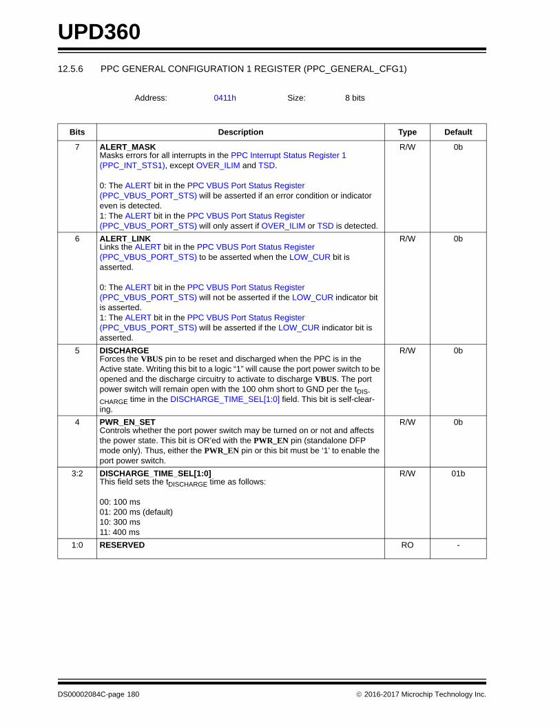
UPD360
12.5.6 PPC GENERAL CONFIGURATION 1 REGISTER (PPC_GENERAL_CFG1)
Address: 0411h Size: 8 bits
Bits Description Type Default
7 ALERT_MASKMasks errors for all interrupts in the PPC Interrupt Status Register 1 (PPC_INT_STS1), except OVER_ILIM and TSD.
0: The ALERT bit in the PPC VBUS Port Status Register (PPC_VBUS_PORT_STS) will be asserted if an error condition or indicator even is detected.1: The ALERT bit in the PPC VBUS Port Status Register (PPC_VBUS_PORT_STS) will only assert if OVER_ILIM or TSD is detected.
R/W 0b
6 ALERT_LINKLinks the ALERT bit in the PPC VBUS Port Status Register (PPC_VBUS_PORT_STS) to be asserted when the LOW_CUR bit is asserted.
0: The ALERT bit in the PPC VBUS Port Status Register (PPC_VBUS_PORT_STS) will not be asserted if the LOW_CUR indicator bit is asserted.1: The ALERT bit in the PPC VBUS Port Status Register (PPC_VBUS_PORT_STS) will be asserted if the LOW_CUR indicator bit is asserted.
R/W 0b
5 DISCHARGEForces the VBUS pin to be reset and discharged when the PPC is in the Active state. Writing this bit to a logic “1” will cause the port power switch to be opened and the discharge circuitry to activate to discharge VBUS. The port power switch will remain open with the 100 ohm short to GND per the tDIS-
CHARGE time in the DISCHARGE_TIME_SEL[1:0] field. This bit is self-clear-ing.
R/W 0b
4 PWR_EN_SETControls whether the port power switch may be turned on or not and affects the power state. This bit is OR’ed with the PWR_EN pin (standalone DFP mode only). Thus, either the PWR_EN pin or this bit must be ‘1’ to enable the port power switch.
R/W 0b
3:2 DISCHARGE_TIME_SEL[1:0]This field sets the tDISCHARGE time as follows:
00: 100 ms01: 200 ms (default)10: 300 ms11: 400 ms
R/W 01b
1:0 RESERVED RO -
DS00002084C-page 180 2016-2017 Microchip Technology Inc.

UPD360
12.5.7 PPC GENERAL CONFIGURATION 3 REGISTER (PPC_GENERAL_CFG3)
12.5.8 PPC CURRENT LIMIT REGISTER (PPC_CURRENT_LIMIT)
This register controls the ILIM used by the port power switch. The contents of this register are retained in the Sleep state.Refer to Section 12.3.1, "Current Limiting," on page 172 for additional information.
Note 12-1 When operating in Standalone DFP modes (UPD360-A/UPD360-B only), the default is defined by thePWR_CAP0 and PWR_CAP1 pins.
Address: 0413h Size: 8 bits
Bits Description Type Default
7 PIN_IGNOREWhen set, ignores the PWR_EN pin state (UPD360-A/UPD360-B only) when determining the Active mode selection and power state.
R/W 0b
6:5 RESERVED RO -
4:3 PWR_STATE[1:0]This field indicates the current PPC power state as detailed below. These bits are set and cleared automatically as the power state changes.
00: Sleep 01: Detect 10: Active11: Error
R/W 00b
2 BOOST#Indicates that the IBUS current is >2.0A on VBUS.
R/W 0b
1:0 RESERVED RO -
Address: 0414h Size: 8 bits
Bits Description Type Default
7:3 RESERVED RO -
2:0 ILIM_VBUS[2:0]Sets the ILIM value as follows:
000: 530 mA001: 960 mA010: 1070 mA011: 1280 mA100: 1600 mA101: 2130 mA110: 2670 mA111: 3200 mA
R/W Note 12-1
2016-2017 Microchip Technology Inc. DS00002084C-page 181
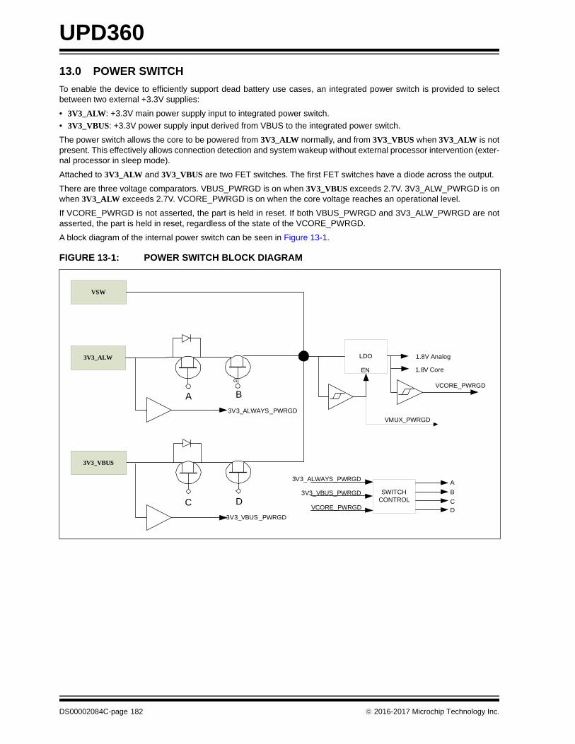
UPD360
13.0 POWER SWITCH
To enable the device to efficiently support dead battery use cases, an integrated power switch is provided to selectbetween two external +3.3V supplies:
• 3V3_ALW: +3.3V main power supply input to integrated power switch.
• 3V3_VBUS: +3.3V power supply input derived from VBUS to the integrated power switch.
The power switch allows the core to be powered from 3V3_ALW normally, and from 3V3_VBUS when 3V3_ALW is notpresent. This effectively allows connection detection and system wakeup without external processor intervention (exter-nal processor in sleep mode).
Attached to 3V3_ALW and 3V3_VBUS are two FET switches. The first FET switches have a diode across the output.
There are three voltage comparators. VBUS_PWRGD is on when 3V3_VBUS exceeds 2.7V. 3V3_ALW_PWRGD is onwhen 3V3_ALW exceeds 2.7V. VCORE_PWRGD is on when the core voltage reaches an operational level.
If VCORE_PWRGD is not asserted, the part is held in reset. If both VBUS_PWRGD and 3V3_ALW_PWRGD are notasserted, the part is held in reset, regardless of the state of the VCORE_PWRGD.
A block diagram of the internal power switch can be seen in Figure 13-1.
FIGURE 13-1: POWER SWITCH BLOCK DIAGRAM
G
3V3_ALW
3V3_VBUS
VSW
LDO
A B
C D
3V3_VBUS_PWRGD
3V3_ALWAYS_PWRGD
VCORE_PWRGD
SWITCHCONTROL
3V3_ALWAYS_PWRGD
3V3_VBUS_PWRGD
VCORE_PWRGD
A
CD
B
1.8V Analog
1.8V CoreEN
VMUX_PWRGD
DS00002084C-page 182 2016-2017 Microchip Technology Inc.

UPD360
13.1 Operation
13.1.1 POWER UP
When the device is powering up, both VBUS_PWRGD and 3V3_ALW_PWRGD are low. Under these conditions,switches A and C are open, B and D are closed. The voltage going to the input of the core regulator is the higher of3V3_ALW and 3V3_VBUS. The diodes prevent back drive.
FIGURE 13-2: POWER SWITCH: POWERING UP
G
3V3_ALW
3V3_VBUS
VSW
A B
C D
3V3_VBUS_PWRGD=0
3V3_ALWAYS_PWRGD=0
SWITCHCONTROL
3V3_ALWAYS_PWRGD
3V3_VBUS_PWRGD
VCORE_PWRGD
A
C
D
B
LDOs
VCORE_PWRGD
1.8V Analog
1.8V CoreEN
VMUX_PWRGD
2016-2017 Microchip Technology Inc. DS00002084C-page 183

UPD360
13.1.2 3V3_ALW ONLY POWERS UP
In this case, only 3V3_ALW powers up (VBUS_PWRGD = 0 and 3V3_ALW_PWRGD = 1). When this occurs, FETswitch D is opened. After 50us, FET switch A is shorted. This sequence eliminates the possibility of back-drive whenthe diode is shorted to eliminate the voltage drop.
FIGURE 13-3: POWER SWITCH: POWERING UP STEP ONE
FIGURE 13-4: POWER SWITCH: POWERING UP STEP TWO
G
3V3_ALW
3V3_VBUS
VSW
A B
C D
VBUS_PWRGD=0
3V3_ALWAYS_PWRGD=1
SWITCHCONTROL
3V3_ALWAYS_PWRGD
3V3_VBUS_PWRGD
VCORE_PWRGD
A
CD
B
3V3_ALW-0.7V
LDOs
VCORE_PWRGD
1.8V Analog
1.8V CoreEN
VMUX_PWRGD
G
3V3_ALW
3V3_VBUS
VSW
A B
C D
3V3_VBUS_PWRGD =0
3V3_ALWAYS_PWRGD=1
3V3_ALW
LDOs
VCORE_PWRGD
1.8V Analog
1.8V CoreEN
VMUX_PWRGD
SWITCHCONTROL
3V3_ALWAYS_PWRGD
3V3_VBUS_PWRGD
VCORE_PWRGD
A
C
D
B
DS00002084C-page 184 2016-2017 Microchip Technology Inc.

UPD360
13.1.3 VBUS ONLY POWERS UP
This is the opposite example from the previous case. In this case, only VBUS powers up (3V3_ALW_PWRGD = 0throughout, and VBUS_PWRGD = 1 when the threshold is hit). Once VBUS_PWRGD is valid, the internal regulator isturned on and normal operation begins. At no time during this process is the 3V3_ALW rail back driven.
FIGURE 13-5: POWER SWITCH: VBUS ONLY POWER UP STEP ONE
FIGURE 13-6: POWER SWITCH: VBUS ONLY POWER UP STEP TWO
G
3V3_ALW
3V3_VBUS
VSW
A B
C D
3V3_VBUS_PWRGD=1
3V3_ALWAYS_PWRGD=0
3V3_VBUS-0.7V
LDOs
VCORE_PWRGD
1.8V Analog
1.8V CoreEN
VMUX_PWRGD
SWITCHCONTROL
3V3_ALWAYS_PWRGD
3V3_VBUS_PWRGD
VCORE_PWRGD
A
CD
B
3V3_ALW
3V3_VBUS
VSW
A B
C D
3V3_VBUS_PWRGD=1
3V3_ALWAYS_PWRGD=0
SWITCHCONTROL
3V3_ALWAYS_PWRGD
3V3_VBUS_PWRGD
VCORE_PWRGD
A
C
D
B
3V3_VBUS
LDOs
VCORE_PWRGD
1.8V Analog
1.8V CoreEN
VMUX_PWRGD
2016-2017 Microchip Technology Inc. DS00002084C-page 185

UPD360
13.1.4 VBUS POWERED UP FOLLOWED BY 3V3_ALW COMING UP
In this case, VBUS is already powered up and 3V3_ALW starts to come up (and will take over and power the core).Figure 13-7 shows the VBUS only state.
Once 3V3_ALW_PWRGD is detected, FET switch C is opened. The diode is required because 3V3_ALW could begreater than or less than VBUS. The voltage at the input to the LDO drops to 3V3_VBUS-0.7V.
FIGURE 13-7: POWER SWITCH: VBUS FOLLOWED BY 3V3_ALW STEP ONE
FIGURE 13-8: POWER SWITCH: VBUS FOLLOWED BY 3V3_ALW STEP TWO
3V3_ALW
3V3_VBUS
VSW
A B
C D
3V3_VBUS_PWRGD=1
3V3_VBUS
LDOs
VCORE_PWRGD
1.8V Analog
1.8V CoreEN
VMUX_PWRGD3V3_ALWAYS _PWRGD=0
SWITCHCONTROL
3V3_ALWAYS _PWRGD
3V3_VBUS_PWRGD
VCORE_PWRGD
A
C
D
B
3V3_ALW
3V3_VBUS
VSW
A B
C D
3V3_VBUS_PWRGD=1
3V3_ALWAYS_PWRGD=1
3V3_VBUS-0.7
LDOs
VCORE_PWRGD
1.8V Analog
1.8V CoreEN
VMUX_PWRGD
SWITCHCONTROL
3V3_ALWAYS_PWRGD
3V3_VBUS_PWRGD
VCORE_PWRGD
A
C
D
B
DS00002084C-page 186 2016-2017 Microchip Technology Inc.
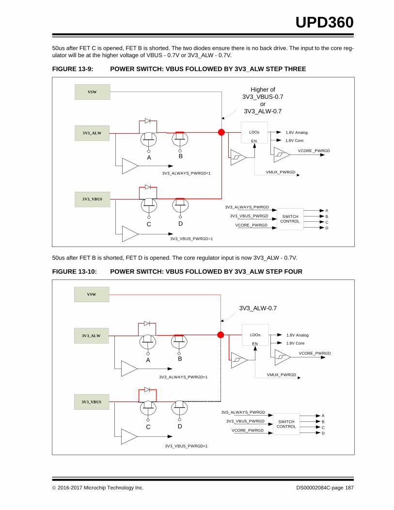
UPD360
50us after FET C is opened, FET B is shorted. The two diodes ensure there is no back drive. The input to the core reg-ulator will be at the higher voltage of VBUS - 0.7V or 3V3_ALW - 0.7V.
50us after FET B is shorted, FET D is opened. The core regulator input is now 3V3_ALW - 0.7V.
FIGURE 13-9: POWER SWITCH: VBUS FOLLOWED BY 3V3_ALW STEP THREE
FIGURE 13-10: POWER SWITCH: VBUS FOLLOWED BY 3V3_ALW STEP FOUR
3V3_ALW
3V3_VBUS
VSW
A B
C D
3V3_VBUS_PWRGD=1
3V3_ALWAYS_PWRGD=1
Higher of 3V3_VBUS-0.7
or3V3_ALW-0.7
LDOs
VCORE_PWRGD
1.8V Analog
1.8V CoreEN
VMUX_PWRGD
SWITCHCONTROL
3V3_ALWAYS_PWRGD
3V3_VBUS_PWRGD
VCORE_PWRGD
A
C
D
B
3V3_ALW
3V3_VBUS
VSW
A B
C D
3V3_VBUS_PWRGD=1
3V3_ALWAYS_PWRGD=1
3V3_ALW-0.7
LDOs
VCORE_PWRGD
1.8V Analog
1.8V CoreEN
VMUX_PWRGD
SWITCHCONTROL
3V3_ALWAYS_PWRGD
3V3_VBUS_PWRGD
VCORE_PWRGD
A
C
D
B
2016-2017 Microchip Technology Inc. DS00002084C-page 187
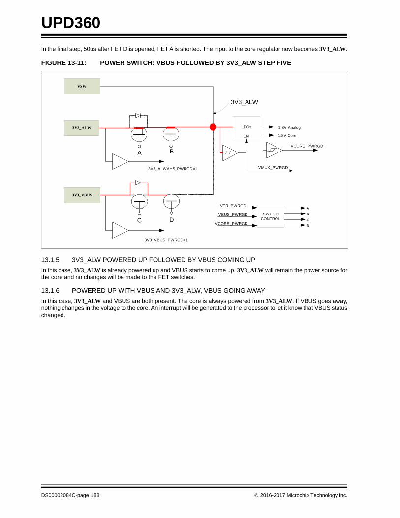
UPD360
In the final step, 50us after FET D is opened, FET A is shorted. The input to the core regulator now becomes 3V3_ALW.
13.1.5 3V3_ALW POWERED UP FOLLOWED BY VBUS COMING UP
In this case, 3V3_ALW is already powered up and VBUS starts to come up. 3V3_ALW will remain the power source forthe core and no changes will be made to the FET switches.
13.1.6 POWERED UP WITH VBUS AND 3V3_ALW, VBUS GOING AWAY
In this case, 3V3_ALW and VBUS are both present. The core is always powered from 3V3_ALW. If VBUS goes away,nothing changes in the voltage to the core. An interrupt will be generated to the processor to let it know that VBUS statuschanged.
FIGURE 13-11: POWER SWITCH: VBUS FOLLOWED BY 3V3_ALW STEP FIVE
3V3_ALW
3V3_VBUS
VSW
A B
C D
3V3_VBUS_PWRGD=1
3V3_ALWAYS_PWRGD=1
SWITCHCONTROL
VTR_PWRGD
VBUS_PWRGD
VCORE_PWRGD
A
C
D
B
3V3_ALW
LDOs
VCORE_PWRGD
1.8V Analog
1.8V CoreEN
VMUX_PWRGD
DS00002084C-page 188 2016-2017 Microchip Technology Inc.
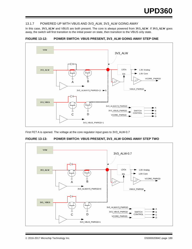
UPD360
13.1.7 POWERED UP WITH VBUS AND 3V3_ALW, 3V3_ALW GOING AWAY
In this case, 3V3_ALW and VBUS are both present. The core is always powered from 3V3_ALW. If 3V3_ALW goesaway, the switch will first transition to the initial power on state, then transition to the VBUS only state.
First FET A is opened. The voltage at the core regulator input goes to 3V3_ALW-0.7
FIGURE 13-12: POWER SWITCH: VBUS PRESENT, 3V3_ALW GOING AWAY STEP ONE
FIGURE 13-13: POWER SWITCH: VBUS PRESENT, 3V3_ALW GOING AWAY STEP TWO
G
3V3_ALW
3V3_VBUS
VSW
A B
C D
3V3_VBUS_PWRGD=1
3V3_ALWAYS_PWRGD=(1 0)
3V3_ALW
LDOs
VCORE_PWRGD
1.8V Analog
1.8V CoreEN
VMUX_PWRGD
SWITCHCONTROL
3V3_ALWAYS_PWRGD
3V3_VBUS_PWRGD
VCORE_PWRGD
A
C
D
B
3V3_ALW
3V3_ VBUS
VSW
A B
C D
3V3_VBUS_PWRGD=1
3V3_ALWAYS_PWRGD=0
3V3_ALW-0.7
LDOs
VCORE_PWRGD
1.8V Analog
1.8V CoreEN
VMUX_PWRGD
SWITCHCONTROL
3V3_ALWAYS_PWRGD
3V3_VBUS_PWRGD
VCORE_PWRGD
A
CD
B
2016-2017 Microchip Technology Inc. DS00002084C-page 189

UPD360
50uS later, the FET is closed. The voltage at the input of the core regulator will be the higher of 3V3_ALW-0.7 or 3V3_V-BUS -0.7.
50uS later, FET B is opened. The voltage at the input of the core regulator is VBUS-0.7.
FIGURE 13-14: POWER SWITCH: VBUS PRESENT, 3V3_ALW GOING AWAY STEP THREE
FIGURE 13-15: POWER SWITCH: VBUS PRESENT, 3V3_ALW GOING AWAY STEP FOUR
3V3_ALW
3V3_ VBUS
VSW
A B
C D
3V3_VBUS_PWRGD=1
3V3_ALWAYS_PWRGD=0
Higher of 3V3_ALW – 0.7
Or3V3_VBUS – 0.7
LDOs
VCORE_PWRGD
1.8V Analog
1.8V CoreEN
VMUX_PWRGD
SWITCHCONTROL
3V3_ALWAYS_PWRGD
3V3_VBUS_PWRGD
VCORE_PWRGD
A
C
D
B
3V3_ALW
3V3_ VBUS
VSW
A B
C D
3V3_VBUS_PWRGD=1
3V3_ALWAYS_PWRGD=0
3V3_VBUS-0.7V
LDOs
VCORE_PWRGD
1.8V Analog
1.8V CoreEN
VMUX_PWRGD
SWITCHCONTROL
3V3_ALWAYS_PWRGD
3V3_VBUS_PWRGD
VCORE_PWRGD
A
C
D
B
DS00002084C-page 190 2016-2017 Microchip Technology Inc.
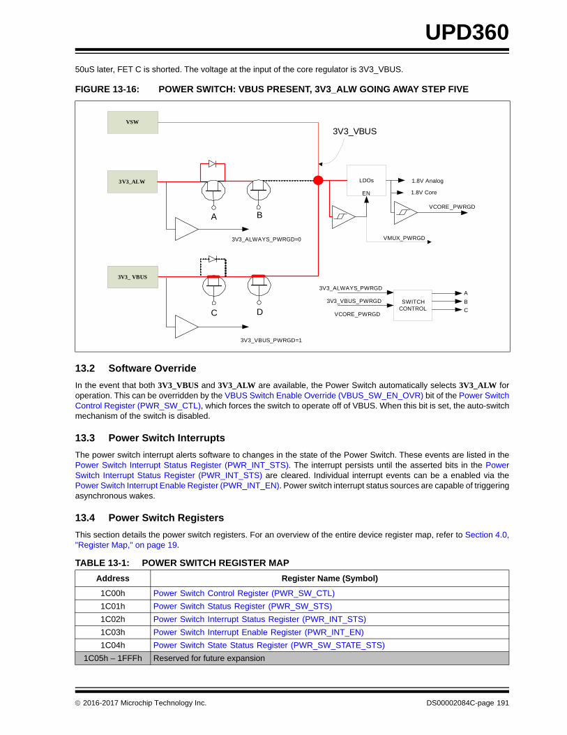
UPD360
50uS later, FET C is shorted. The voltage at the input of the core regulator is 3V3_VBUS.
13.2 Software Override
In the event that both 3V3_VBUS and 3V3_ALW are available, the Power Switch automatically selects 3V3_ALW foroperation. This can be overridden by the VBUS Switch Enable Override (VBUS_SW_EN_OVR) bit of the Power SwitchControl Register (PWR_SW_CTL), which forces the switch to operate off of VBUS. When this bit is set, the auto-switchmechanism of the switch is disabled.
13.3 Power Switch Interrupts
The power switch interrupt alerts software to changes in the state of the Power Switch. These events are listed in thePower Switch Interrupt Status Register (PWR_INT_STS). The interrupt persists until the asserted bits in the PowerSwitch Interrupt Status Register (PWR_INT_STS) are cleared. Individual interrupt events can be a enabled via thePower Switch Interrupt Enable Register (PWR_INT_EN). Power switch interrupt status sources are capable of triggeringasynchronous wakes.
13.4 Power Switch Registers
This section details the power switch registers. For an overview of the entire device register map, refer to Section 4.0,"Register Map," on page 19.
FIGURE 13-16: POWER SWITCH: VBUS PRESENT, 3V3_ALW GOING AWAY STEP FIVE
TABLE 13-1: POWER SWITCH REGISTER MAP
Address Register Name (Symbol)
1C00h Power Switch Control Register (PWR_SW_CTL)
1C01h Power Switch Status Register (PWR_SW_STS)
1C02h Power Switch Interrupt Status Register (PWR_INT_STS)
1C03h Power Switch Interrupt Enable Register (PWR_INT_EN)
1C04h Power Switch State Status Register (PWR_SW_STATE_STS)
1C05h – 1FFFh Reserved for future expansion
3V3_ALW
3V3_ VBUS
VSW
A B
C D
3V3_VBUS_PWRGD=1
3V3_ALWAYS_PWRGD=0
3V3_VBUS
LDOs
VCORE_PWRGD
1.8V Analog
1.8V CoreEN
VMUX_PWRGD
SWITCHCONTROL
3V3_ALWAYS_PWRGD
3V3_VBUS_PWRGD
VCORE_PWRGD
A
C
B
2016-2017 Microchip Technology Inc. DS00002084C-page 191

UPD360
13.4.1 POWER SWITCH CONTROL REGISTER (PWR_SW_CTL)
13.4.2 POWER SWITCH STATUS REGISTER (PWR_SW_STS)
Address: 1C00h Size: 8 bits
Bits Description Type Default
7:2 RESERVED RO -
1 Power Switch Enable (PM_SW_ENB)This active low signal enables the power switch.
R/W 0b
0 VBUS Switch Enable Override (VBUS_SW_EN_OVR)When this bit is asserted, the power switch utilizes the 3V3_VBUS supply. This bit only has meaning if the device is currently operating on 3V3_ALW and the VBUS supply is present.
This bit disables the auto-switch mechanism of the power switch.
R/W 0b
Address: 1C01h Size: 8 bits
Bits Description Type Default
7:6 RESERVED RO -
5 3V3_ALW POR (3V3_ALW_RDY)POR output from the main VBAT external supply. Active high when the supply is above 2.85V. Active low when the supply drops below 2.7V.
RO 0b
4 3V3_VBUS POR (VBUS_RDY)POR output from the VBUS external supply. Active high when the supply is above 4V. Active low when the supply drops below 2.7V.
RO 0b
3 RESERVED RO -
2 PWR_RDYIndicates power ready on VSW and VDD18 supplies.
RO 1b
1 3V3_ALW Switch Gate Off (3V3_ALW_SW_OKB)Indicates state of VSW with respect to 3V3_ALW.
0: VSW < 3V3_ALW1: VSW > 3V3_ALW
RO 0b
0 VBUS Switch Gate Off (VBUS_SW_OKB)Indicates state of VSW with respect to VBUS.
0: VSW < VBUS1: VSW > VBUS
RO 0b
DS00002084C-page 192 2016-2017 Microchip Technology Inc.
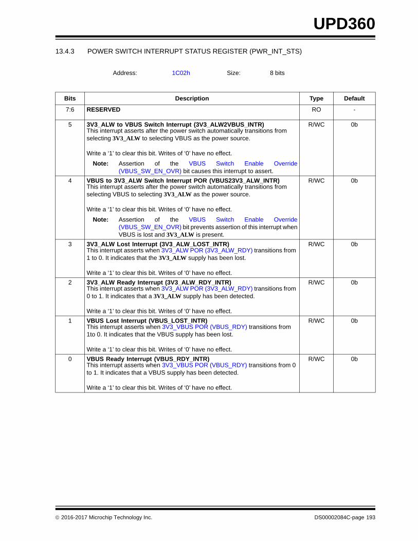
UPD360
13.4.3 POWER SWITCH INTERRUPT STATUS REGISTER (PWR_INT_STS)
Address: 1C02h Size: 8 bits
Bits Description Type Default
7:6 RESERVED RO -
5 3V3_ALW to VBUS Switch Interrupt (3V3_ALW2VBUS_INTR)This interrupt asserts after the power switch automatically transitions from selecting 3V3_ALW to selecting VBUS as the power source.
Write a ‘1’ to clear this bit. Writes of ‘0’ have no effect.
Note: Assertion of the VBUS Switch Enable Override(VBUS_SW_EN_OVR) bit causes this interrupt to assert.
R/WC 0b
4 VBUS to 3V3_ALW Switch Interrupt POR (VBUS23V3_ALW_INTR)This interrupt asserts after the power switch automatically transitions from selecting VBUS to selecting 3V3_ALW as the power source.
Write a ‘1’ to clear this bit. Writes of ‘0’ have no effect.
Note: Assertion of the VBUS Switch Enable Override(VBUS_SW_EN_OVR) bit prevents assertion of this interrupt whenVBUS is lost and 3V3_ALW is present.
R/WC 0b
3 3V3_ALW Lost Interrupt (3V3_ALW_LOST_INTR)This interrupt asserts when 3V3_ALW POR (3V3_ALW_RDY) transitions from 1 to 0. It indicates that the 3V3_ALW supply has been lost.
Write a ‘1’ to clear this bit. Writes of ‘0’ have no effect.
R/WC 0b
2 3V3_ALW Ready Interrupt (3V3_ALW_RDY_INTR)This interrupt asserts when 3V3_ALW POR (3V3_ALW_RDY) transitions from 0 to 1. It indicates that a 3V3_ALW supply has been detected.
Write a ‘1’ to clear this bit. Writes of ‘0’ have no effect.
R/WC 0b
1 VBUS Lost Interrupt (VBUS_LOST_INTR)This interrupt asserts when 3V3_VBUS POR (VBUS_RDY) transitions from 1to 0. It indicates that the VBUS supply has been lost.
Write a ‘1’ to clear this bit. Writes of ‘0’ have no effect.
R/WC 0b
0 VBUS Ready Interrupt (VBUS_RDY_INTR)This interrupt asserts when 3V3_VBUS POR (VBUS_RDY) transitions from 0 to 1. It indicates that a VBUS supply has been detected.
Write a ‘1’ to clear this bit. Writes of ‘0’ have no effect.
R/WC 0b
2016-2017 Microchip Technology Inc. DS00002084C-page 193
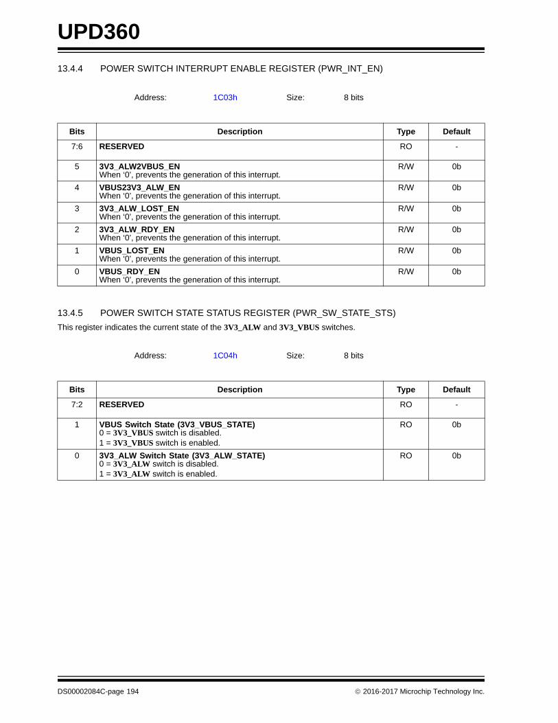
UPD360
13.4.4 POWER SWITCH INTERRUPT ENABLE REGISTER (PWR_INT_EN)
13.4.5 POWER SWITCH STATE STATUS REGISTER (PWR_SW_STATE_STS)
This register indicates the current state of the 3V3_ALW and 3V3_VBUS switches.
Address: 1C03h Size: 8 bits
Bits Description Type Default
7:6 RESERVED RO -
5 3V3_ALW2VBUS_ENWhen ‘0’, prevents the generation of this interrupt.
R/W 0b
4 VBUS23V3_ALW_ENWhen ‘0’, prevents the generation of this interrupt.
R/W 0b
3 3V3_ALW_LOST_ENWhen ‘0’, prevents the generation of this interrupt.
R/W 0b
2 3V3_ALW_RDY_ENWhen ‘0’, prevents the generation of this interrupt.
R/W 0b
1 VBUS_LOST_ENWhen ‘0’, prevents the generation of this interrupt.
R/W 0b
0 VBUS_RDY_ENWhen ‘0’, prevents the generation of this interrupt.
R/W 0b
Address: 1C04h Size: 8 bits
Bits Description Type Default
7:2 RESERVED RO -
1 VBUS Switch State (3V3_VBUS_STATE)0 = 3V3_VBUS switch is disabled.1 = 3V3_VBUS switch is enabled.
RO 0b
0 3V3_ALW Switch State (3V3_ALW_STATE)0 = 3V3_ALW switch is disabled.1 = 3V3_ALW switch is enabled.
RO 0b
DS00002084C-page 194 2016-2017 Microchip Technology Inc.

UPD360
14.0 DISPLAYPORT HOT PLUG DETECT (HPD)
14.1 Overview
The device provides hardware offload support for detecting the state of a Display Port compliant HPD input pin to thedevice.
The USB Type-C DisplayPort Alternate Mode Specification defines the HPD state in terms of two status flags:
• HPD_STATE: Indicates whether the HPD’s logical state is high or low (denoted as HPD_HIGH or HPD_LOW, respectively). For the purposes of communicating the HPD state over USB, the logical state of HPD is considered as remaining high while receiving an IRQ_HPD, and is low during the time that HPD is being de-bounced on a new mechanical connection. The logical state of HPD transitions from high to low when a low level on the HPD link has been detected for 2ms (i.e., longer than the maximum IRQ_HPD pulse detection time). The logical state of HPD is unchanged during glitches (as specified in DP v1.3) on the HPD link.
• IRQ_HPD: Indicates an IRQ_HPD (i.e., a high-to-low transition on HPD followed by a low-to-high transition was detected between 250us and 2ms later, as specified in DP v1.3).
14.2 HPD Receiver
The device provides HPD detection (input) via the HPD pin. HPD detection is enabled by setting HPD Enable bit andconfiguring the HPD pin to be an input via HPD Configuration in HPD Control Register (HPD_CTL). Upon setting thisbit, the device continuously monitors the state of the HPD pin as follows:
• When an IRQ_HPD event occurs, the IRQ_HPD interrupt bit in HPD Interrupt Status Register (HPD_INT_STS) will assert. IRQ_HPD is detected when HPD is initially high and de-asserts for a time greater than or equal to the value in the IRQ_HPD Minimum Time Register (IRQ_HPD_MIN_TIME) and less than or equal to the value in the IRQ_HPD Maximum Time Register (IRQ_HPD_MAX_TIME).
• When a Low to High transition is debounced and detected, the HPD_HIGH interrupt bit in HPD Interrupt Status Register (HPD_INT_STS) will assert. HPD_HIGH is detected when the HPD pin is initially low and asserts for a time greater than or equal to the value in the HPD High Detect Time Register (HPD_HIGH_DET_TIME).
• When a High to Low transition is debounced and detected, the HPD_LOW interrupt bit in HPD Interrupt Status Register (HPD_INT_STS) will assert. HPD_LOW is detected when HPD pin is initially low and asserts for a time greater than or equal to the value in the HPD Low Detect Time Register (HPD_LOW_DET_TIME).
APPLICATION NOTE: The HPD Interrupt Status Register (HPD_INT_STS) contents are reset to 00h when HPDEnable is cleared.
APPLICATION NOTE: Enabled and asserted interrupts trigger the HPD_INT interrupt in the Interrupt Status Register(INT_STS).
A mechanism has been added via the HPD Event Queue Register (HPD_QUEUE) to record up to four HPD events.This function is enabled when HPD Enable is set and HPD Configuration indicates the HPD pin is operating as an input.See Section 14.4.4, "HPD Event Queue Register (HPD_QUEUE)," on page 199 for additional details.
APPLICATION NOTE: The state of the HPD pin is available by reading HPD State in HPD Control Register(HPD_CTL).
This feature is used as follows:
1. Software configures IRQ_HPD Minimum Time Register (IRQ_HPD_MIN_TIME), IRQ_HPD Maximum Time Reg-ister (IRQ_HPD_MAX_TIME), HPD High Detect Time Register (HPD_HIGH_DET_TIME) and HPD Low DetectTime Register (HPD_LOW_DET_TIME). To comply with the DisplayPort specification for IRQ_HPD, theIRQ_HPD Minimum Time Register (IRQ_HPD_MIN_TIME) and IRQ_HPD Maximum Time Register (IRQ_HPD_-MAX_TIME) should be configured to 250 us and 2 ms, respectively. Likewise, HPD Low Detect Time Register(HPD_LOW_DET_TIME) should be configured to greater than 2 ms.
2. If desired, interrupts may be enabled by asserting the respective bits in the HPD Interrupt Enable Register(HPD_INT_EN).
3. HPD Enable is set and HPD Configuration is cleared in the HPD Control Register (HPD_CTL).
Note: The HPD pin is always configured as a push/pull driver.
2016-2017 Microchip Technology Inc. DS00002084C-page 195

UPD360
4. When an Hot Plug event occurs, the HPD Event Queue Register (HPD_QUEUE) is updated and an interrupt willassert if configured.
5. HPD state changes are reflected by assertion of QUEUE_NOT_EMPTY, HPD_HIGH, HPD_LOW and IRQ_HPDbits in HPD Interrupt Status Register (HPD_INT_STS). They may cause assertion of HPD_INT in the InterruptStatus Register (INT_STS), if enabled.
6. Software reads the HPD Event Queue Register (HPD_QUEUE) to determine the Hot Plug events received.
7. Software writes to the HPD Event Queue Register (HPD_QUEUE) and clears the valid entries.
14.3 HPD Transmission
The device provides HPD transmission (output) via the HPD pin. This is done via the HPD Control Register (HPD_CTL)by setting both HPD Configuration and HPD Enable to “1”. The value driven on the HPD pin is controlled by HPD OutputValue.
Support is also provided for generating an IRQ_HPD. This is accomplished by programming the deassertion time inHPD IRQ Generation Time Register (HPD_IRQ_GEN) and then setting Generate IRQ in HPD Control Register(HPD_CTL). Generate IRQ self clears after the interrupt pulse is issued.
This feature is used as follows:
1. Configure the HPD pin as an output by setting HPD Configuration and HPD Enable in HPD Control Register(HPD_CTL). The value for HPD is defined by the value programmed in HPD Output Value.
2. If it is desired to generate an IRQ_HPD, the HPD IRQ Generation Time Register (HPD_IRQ_GEN) must be pro-grammed with the desired HPD deassertion time.
3. If it is desired to receive an interrupt upon generation of IRQ_HPD, the respective bit in the HPD Interrupt EnableRegister (HPD_INT_EN) should be enabled.
4. Software requests IRQ_HPD generation by setting Generate IRQ in the HPD Control Register (HPD_CTL). HPDOutput Value must also be set to 1b.
5. Upon generating the IRQ_HPD interrupt, the Generate IRQ bit will self clear.
6. The IRQ_HPD bit asserts in the HPD Interrupt Status Register (HPD_INT_STS) and shall cause assertion of theHPD_INT interrupt in the Interrupt Status Register (INT_STS), if enabled.
14.4 DisplayPort HPD Registers
This section details the DisplayPort HPD registers. For an overview of the entire device register map, refer to Section4.0, "Register Map," on page 19.
TABLE 14-1: DISPLAYPORT HPD REGISTER MAP
Address Register Name (Symbol)
0C00h HPD Control Register (HPD_CTL)
0C01h HPD Interrupt Status Register (HPD_INT_STS)
0C02h HPD Interrupt Enable Register (HPD_INT_EN)
0C03h HPD Event Queue Register (HPD_QUEUE)
0C04h IRQ_HPD Minimum Time Register (IRQ_HPD_MIN_TIME)
0C05h IRQ_HPD Maximum Time Register (IRQ_HPD_MAX_TIME)
0C06h HPD High Detect Time Register (HPD_HIGH_DET_TIME)
0C08h HPD Low Detect Time Register (HPD_LOW_DET_TIME)
0C0Ah HPD IRQ Generation Time Register (HPD_IRQ_GEN)
0C0Bh – 0FFFh Reserved for future expansion
Note: RESERVED address space must not be written under any circumstances. Failure to heed this warn-ing may result in untoward operation and unexpected results.
DS00002084C-page 196 2016-2017 Microchip Technology Inc.
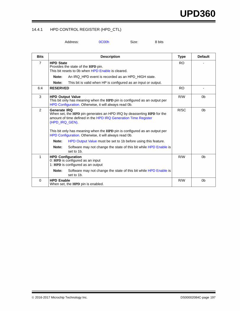
UPD360
14.4.1 HPD CONTROL REGISTER (HPD_CTL)
Address: 0C00h Size: 8 bits
Bits Description Type Default
7 HPD StateProvides the state of the HPD pin.This bit resets to 0b when HPD Enable is cleared.
Note: An IRQ_HPD event is recorded as an HPD_HIGH state.
Note: This bit is valid when HP is configured as an input or output.
RO -
6:4 RESERVED RO -
3 HPD Output ValueThis bit only has meaning when the HPD pin is configured as an output per HPD Configuration. Otherwise, it will always read 0b.
R/W 0b
2 Generate IRQWhen set, the HPD pin generates an HPD IRQ by deasserting HPD for the amount of time defined in the HPD IRQ Generation Time Register (HPD_IRQ_GEN).
This bit only has meaning when the HPD pin is configured as an output per HPD Configuration. Otherwise, it will always read 0b.
Note: HPD Output Value must be set to 1b before using this feature.
Note: Software may not change the state of this bit while HPD Enable isset to 1b.
R/SC 0b
1 HPD Configuration0: HPD is configured as an input1: HPD is configured as an output
Note: Software may not change the state of this bit while HPD Enable isset to 1b.
R/W 0b
0 HPD EnableWhen set, the HPD pin is enabled.
R/W 0b
2016-2017 Microchip Technology Inc. DS00002084C-page 197

UPD360
14.4.2 HPD INTERRUPT STATUS REGISTER (HPD_INT_STS)
The contents of this register reset to 00h when the HPD Enable bit in the HPD Control Register (HPD_CTL) is cleared.
Address: 0C01h Size: 8 bits
BITS DESCRIPTION TYPE DEFAULT
7:4 RESERVED RO -
3 QUEUE_NOT_EMPTYIndicates that the HPD Event Queue Register (HPD_QUEUE) is not empty.
Note: This interrupt is cleared after HPD Event Queue Register (HPD_-QUEUE) is read.
Note: This bit only has meaning when the HPD pin is configured as aninput.
RO 0b
2 HPD_HIGHWhen set, indicates that an HPD Low to High transition has been detected.
Note: The source of this input is a pulse and does not persist after beingcleared.
Note: This bit only has meaning when the HPD pin is configured as aninput.
R/WC 0b
1 HPD_LOWWhen set, indicates that an HPD High to Low transition has been detected.
Note: The source of this input is a pulse and does not persist after beingcleared.
Note: This bit only has meaning when the HPD pin is configured as aninput.
R/WC 0b
0 IRQ_HPDWhen set, indicates that an HPD IRQ has been detected.
Note: The source of this input is a pulse and does not persist after beingcleared.
Note: When the HPD pin is configured as an input, this bit indicates thatan IRQ_HPD has been detected. When the HPD pin is configuredas an output, this pin indicates that the request to generate anIRQ_HPD has completed.
R/WC 0b
DS00002084C-page 198 2016-2017 Microchip Technology Inc.

UPD360
14.4.3 HPD INTERRUPT ENABLE REGISTER (HPD_INT_EN)
14.4.4 HPD EVENT QUEUE REGISTER (HPD_QUEUE)
This register implements a circular queue that records HPD events detected by the device.
As an event is detected, it is written into the next HPD Event status field that is available and initially starts at HPD Event0 out of reset.
After this register is read, any entries with a valid HPD event field are cleared when software writes 01b into the respec-tive locations. The device will keep track of the last valid entry and store the next received event into the next entry. Forexample, if entries 0 and 1 are valid, the device will always place the next event into location 2, regardless of whetheror not entries 0 and 1 have been cleared by software.
The device will only add entries to empty fields. After writing to HPD Event 3, the device will write the next event intoHPD Event 0, if available.
Each field is encoded as follows.
• 00b: HPD event field is empty
• 01b: HPD_HIGH Detected
• 10b: HPD_LOW Detected
• 11b: HPD_IRQ Detected
When HPD Enable is set to 0b and/or HPD Configuration is set to 1b, this register will always read 00h.
After four HPD events are recorded, any future HPD events shall be ignored until HPD event locations are freed up bysoftware.
Address: 0C02h Size: 8 bits
BITS DESCRIPTION TYPE DEFAULT
7:4 RESERVED RO 0h
3:0 HPD Interrupt EnableWhen “0”, prevents generation of the respective interrupt.
R/W 0h
Address: 0C03h Size: 8 bits
BITS DESCRIPTION TYPE DEFAULT
7:6 HPD Event 3 R/WC 00b
5:4 HPD Event 2 R/WC 00b
3:2 HPD Event 1 R/WC 00b
1:0 HPD Event 0 R/WC 00b
2016-2017 Microchip Technology Inc. DS00002084C-page 199
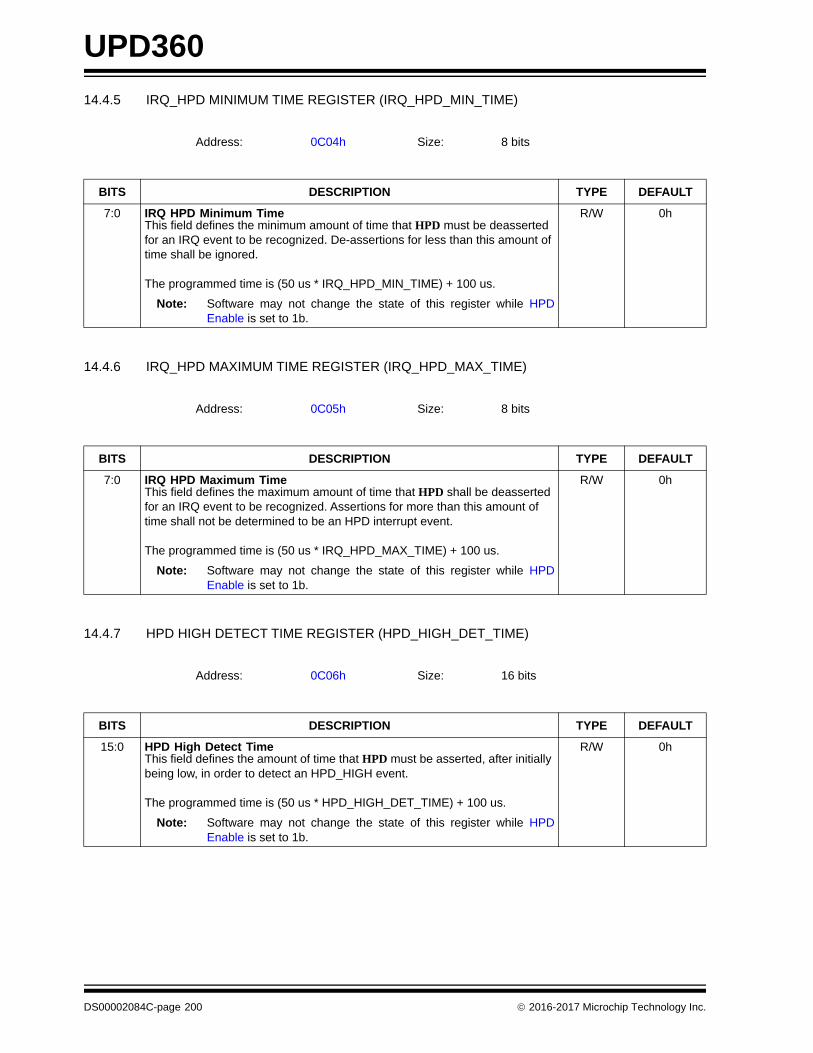
UPD360
14.4.5 IRQ_HPD MINIMUM TIME REGISTER (IRQ_HPD_MIN_TIME)
14.4.6 IRQ_HPD MAXIMUM TIME REGISTER (IRQ_HPD_MAX_TIME)
14.4.7 HPD HIGH DETECT TIME REGISTER (HPD_HIGH_DET_TIME)
Address: 0C04h Size: 8 bits
BITS DESCRIPTION TYPE DEFAULT
7:0 IRQ HPD Minimum TimeThis field defines the minimum amount of time that HPD must be deasserted for an IRQ event to be recognized. De-assertions for less than this amount of time shall be ignored.
The programmed time is (50 us * IRQ_HPD_MIN_TIME) + 100 us.
Note: Software may not change the state of this register while HPDEnable is set to 1b.
R/W 0h
Address: 0C05h Size: 8 bits
BITS DESCRIPTION TYPE DEFAULT
7:0 IRQ HPD Maximum TimeThis field defines the maximum amount of time that HPD shall be deasserted for an IRQ event to be recognized. Assertions for more than this amount of time shall not be determined to be an HPD interrupt event.
The programmed time is (50 us * IRQ_HPD_MAX_TIME) + 100 us.
Note: Software may not change the state of this register while HPDEnable is set to 1b.
R/W 0h
Address: 0C06h Size: 16 bits
BITS DESCRIPTION TYPE DEFAULT
15:0 HPD High Detect TimeThis field defines the amount of time that HPD must be asserted, after initially being low, in order to detect an HPD_HIGH event.
The programmed time is (50 us * HPD_HIGH_DET_TIME) + 100 us.
Note: Software may not change the state of this register while HPDEnable is set to 1b.
R/W 0h
DS00002084C-page 200 2016-2017 Microchip Technology Inc.
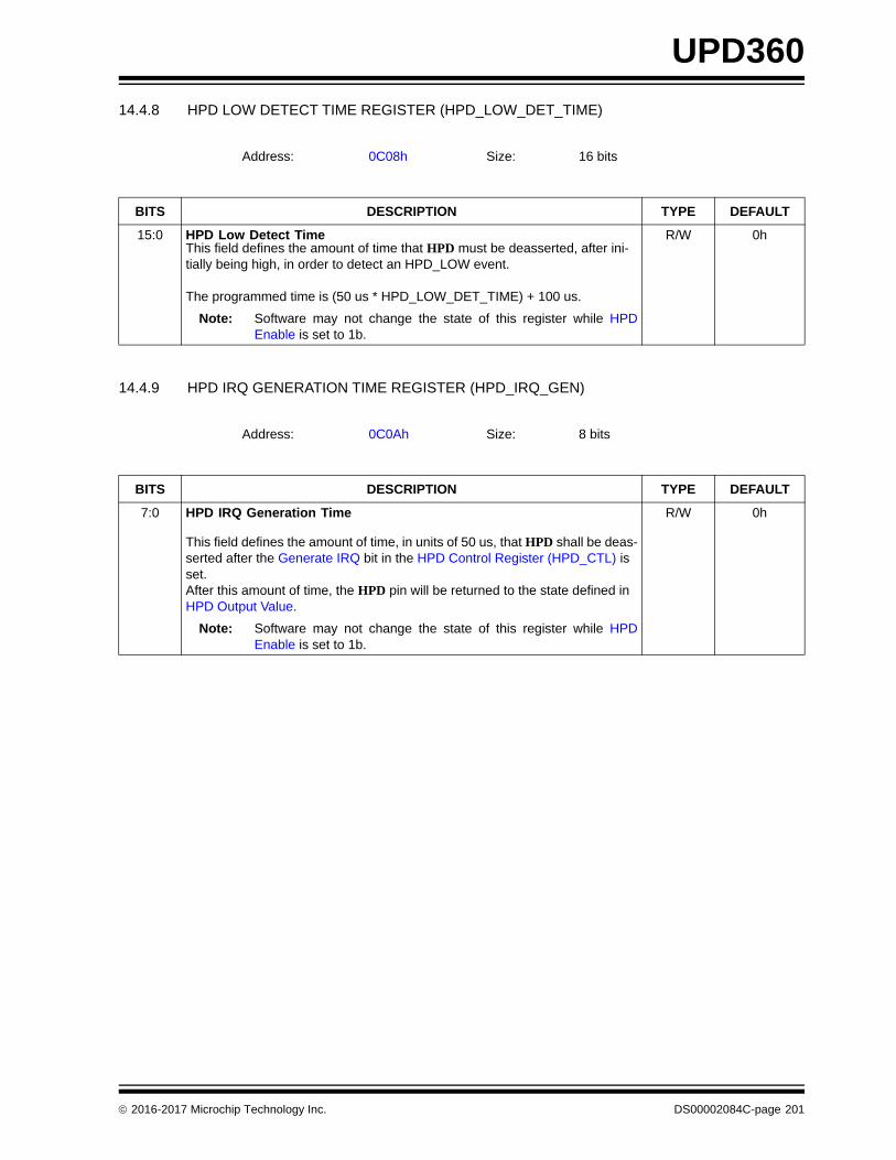
UPD360
14.4.8 HPD LOW DETECT TIME REGISTER (HPD_LOW_DET_TIME)
14.4.9 HPD IRQ GENERATION TIME REGISTER (HPD_IRQ_GEN)
Address: 0C08h Size: 16 bits
BITS DESCRIPTION TYPE DEFAULT
15:0 HPD Low Detect TimeThis field defines the amount of time that HPD must be deasserted, after ini-tially being high, in order to detect an HPD_LOW event.
The programmed time is (50 us * HPD_LOW_DET_TIME) + 100 us.
Note: Software may not change the state of this register while HPDEnable is set to 1b.
R/W 0h
Address: 0C0Ah Size: 8 bits
BITS DESCRIPTION TYPE DEFAULT
7:0 HPD IRQ Generation Time
This field defines the amount of time, in units of 50 us, that HPD shall be deas-serted after the Generate IRQ bit in the HPD Control Register (HPD_CTL) is set.After this amount of time, the HPD pin will be returned to the state defined in HPD Output Value.
Note: Software may not change the state of this register while HPDEnable is set to 1b.
R/W 0h
2016-2017 Microchip Technology Inc. DS00002084C-page 201
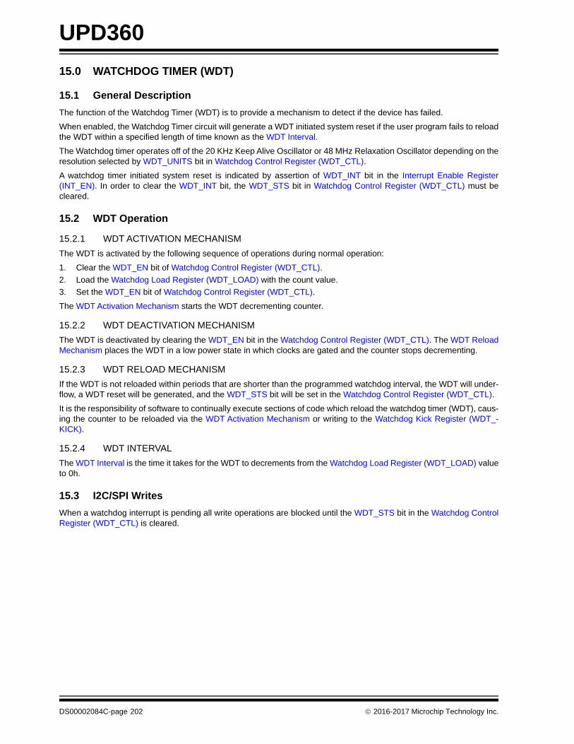
UPD360
15.0 WATCHDOG TIMER (WDT)
15.1 General Description
The function of the Watchdog Timer (WDT) is to provide a mechanism to detect if the device has failed.
When enabled, the Watchdog Timer circuit will generate a WDT initiated system reset if the user program fails to reloadthe WDT within a specified length of time known as the WDT Interval.
The Watchdog timer operates off of the 20 KHz Keep Alive Oscillator or 48 MHz Relaxation Oscillator depending on theresolution selected by WDT_UNITS bit in Watchdog Control Register (WDT_CTL).
A watchdog timer initiated system reset is indicated by assertion of WDT_INT bit in the Interrupt Enable Register(INT_EN). In order to clear the WDT_INT bit, the WDT_STS bit in Watchdog Control Register (WDT_CTL) must becleared.
15.2 WDT Operation
15.2.1 WDT ACTIVATION MECHANISM
The WDT is activated by the following sequence of operations during normal operation:
1. Clear the WDT_EN bit of Watchdog Control Register (WDT_CTL).
2. Load the Watchdog Load Register (WDT_LOAD) with the count value.
3. Set the WDT_EN bit of Watchdog Control Register (WDT_CTL).
The WDT Activation Mechanism starts the WDT decrementing counter.
15.2.2 WDT DEACTIVATION MECHANISM
The WDT is deactivated by clearing the WDT_EN bit in the Watchdog Control Register (WDT_CTL). The WDT ReloadMechanism places the WDT in a low power state in which clocks are gated and the counter stops decrementing.
15.2.3 WDT RELOAD MECHANISM
If the WDT is not reloaded within periods that are shorter than the programmed watchdog interval, the WDT will under-flow, a WDT reset will be generated, and the WDT_STS bit will be set in the Watchdog Control Register (WDT_CTL).
It is the responsibility of software to continually execute sections of code which reload the watchdog timer (WDT), caus-ing the counter to be reloaded via the WDT Activation Mechanism or writing to the Watchdog Kick Register (WDT_-KICK).
15.2.4 WDT INTERVAL
The WDT Interval is the time it takes for the WDT to decrements from the Watchdog Load Register (WDT_LOAD) valueto 0h.
15.3 I2C/SPI Writes
When a watchdog interrupt is pending all write operations are blocked until the WDT_STS bit in the Watchdog ControlRegister (WDT_CTL) is cleared.
DS00002084C-page 202 2016-2017 Microchip Technology Inc.
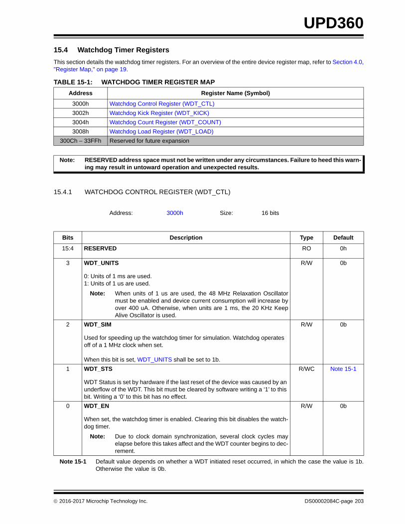
UPD360
15.4 Watchdog Timer Registers
This section details the watchdog timer registers. For an overview of the entire device register map, refer to Section 4.0,"Register Map," on page 19.
15.4.1 WATCHDOG CONTROL REGISTER (WDT_CTL)
Note 15-1 Default value depends on whether a WDT initiated reset occurred, in which the case the value is 1b.Otherwise the value is 0b.
TABLE 15-1: WATCHDOG TIMER REGISTER MAP
Address Register Name (Symbol)
3000h Watchdog Control Register (WDT_CTL)
3002h Watchdog Kick Register (WDT_KICK)
3004h Watchdog Count Register (WDT_COUNT)
3008h Watchdog Load Register (WDT_LOAD)
300Ch – 33FFh Reserved for future expansion
Note: RESERVED address space must not be written under any circumstances. Failure to heed this warn-ing may result in untoward operation and unexpected results.
Address: 3000h Size: 16 bits
Bits Description Type Default
15:4 RESERVED RO 0h
3 WDT_UNITS
0: Units of 1 ms are used.1: Units of 1 us are used.
Note: When units of 1 us are used, the 48 MHz Relaxation Oscillatormust be enabled and device current consumption will increase byover 400 uA. Otherwise, when units are 1 ms, the 20 KHz KeepAlive Oscillator is used.
R/W 0b
2 WDT_SIM
Used for speeding up the watchdog timer for simulation. Watchdog operates off of a 1 MHz clock when set.
When this bit is set, WDT_UNITS shall be set to 1b.
R/W 0b
1 WDT_STS
WDT Status is set by hardware if the last reset of the device was caused by an underflow of the WDT. This bit must be cleared by software writing a ‘1’ to this bit. Writing a ‘0’ to this bit has no effect.
R/WC Note 15-1
0 WDT_EN
When set, the watchdog timer is enabled. Clearing this bit disables the watch-dog timer.
Note: Due to clock domain synchronization, several clock cycles mayelapse before this takes affect and the WDT counter begins to dec-rement.
R/W 0b
2016-2017 Microchip Technology Inc. DS00002084C-page 203
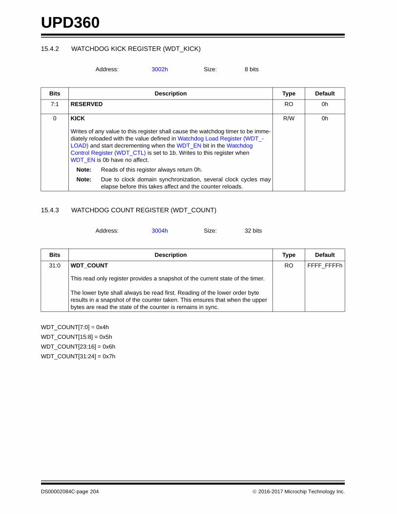
UPD360
15.4.2 WATCHDOG KICK REGISTER (WDT_KICK)
15.4.3 WATCHDOG COUNT REGISTER (WDT_COUNT)
WDT_COUNT[7:0] = 0x4h
WDT_COUNT[15:8] = 0x5h
WDT_COUNT[23:16] = 0x6h
WDT_COUNT[31:24] = 0x7h
Address: 3002h Size: 8 bits
Bits Description Type Default
7:1 RESERVED RO 0h
0 KICK
Writes of any value to this register shall cause the watchdog timer to be imme-diately reloaded with the value defined in Watchdog Load Register (WDT_-LOAD) and start decrementing when the WDT_EN bit in the Watchdog Control Register (WDT_CTL) is set to 1b. Writes to this register when WDT_EN is 0b have no affect.
Note: Reads of this register always return 0h.
Note: Due to clock domain synchronization, several clock cycles mayelapse before this takes affect and the counter reloads.
R/W 0h
Address: 3004h Size: 32 bits
Bits Description Type Default
31:0 WDT_COUNT
This read only register provides a snapshot of the current state of the timer.
The lower byte shall always be read first. Reading of the lower order byte results in a snapshot of the counter taken. This ensures that when the upper bytes are read the state of the counter is remains in sync.
RO FFFF_FFFFh
DS00002084C-page 204 2016-2017 Microchip Technology Inc.

UPD360
15.4.4 WATCHDOG LOAD REGISTER (WDT_LOAD)
WDT_LOAD[7:0] = 0x8h
WDT_LOAD[15:8] = 0x9h
WDT_LOAD[23:16] = 0xAh
WDT_LOAD[31:24] = 0xBh
Address: 3008h Size: 32 bits
Bits Description Type Default
31:0 WDT_LOAD
Writing this register reloads the Watch Dog Timer counter. This register can be programmed only when WDT_EN = 0.
Zero is not a valid load value.
R/W FFFF_FFFFh
2016-2017 Microchip Technology Inc. DS00002084C-page 205
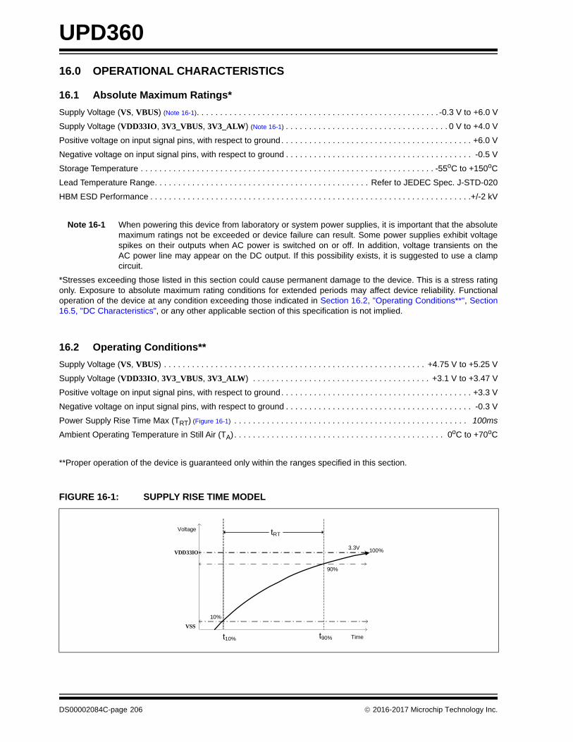
UPD360
16.0 OPERATIONAL CHARACTERISTICS
16.1 Absolute Maximum Ratings*
Supply Voltage (VS, VBUS) (Note 16-1). . . . . . . . . . . . . . . . . . . . . . . . . . . . . . . . . . . . . . . . . . . . . . . . . . . . -0.3 V to +6.0 V
Supply Voltage (VDD33IO, 3V3_VBUS, 3V3_ALW) (Note 16-1) . . . . . . . . . . . . . . . . . . . . . . . . . . . . . . . . . . . 0 V to +4.0 V
Positive voltage on input signal pins, with respect to ground. . . . . . . . . . . . . . . . . . . . . . . . . . . . . . . . . . . . . . . . . +6.0 V
Negative voltage on input signal pins, with respect to ground . . . . . . . . . . . . . . . . . . . . . . . . . . . . . . . . . . . . . . . . -0.5 V
Storage Temperature . . . . . . . . . . . . . . . . . . . . . . . . . . . . . . . . . . . . . . . . . . . . . . . . . . . . . . . . . . . . . . . -55oC to +150oC
Lead Temperature Range. . . . . . . . . . . . . . . . . . . . . . . . . . . . . . . . . . . . . . . . . . . . . . Refer to JEDEC Spec. J-STD-020
HBM ESD Performance . . . . . . . . . . . . . . . . . . . . . . . . . . . . . . . . . . . . . . . . . . . . . . . . . . . . . . . . . . . . . . . . . . . . .+/-2 kV
Note 16-1 When powering this device from laboratory or system power supplies, it is important that the absolutemaximum ratings not be exceeded or device failure can result. Some power supplies exhibit voltagespikes on their outputs when AC power is switched on or off. In addition, voltage transients on theAC power line may appear on the DC output. If this possibility exists, it is suggested to use a clampcircuit.
*Stresses exceeding those listed in this section could cause permanent damage to the device. This is a stress ratingonly. Exposure to absolute maximum rating conditions for extended periods may affect device reliability. Functionaloperation of the device at any condition exceeding those indicated in Section 16.2, "Operating Conditions**", Section16.5, "DC Characteristics", or any other applicable section of this specification is not implied.
16.2 Operating Conditions**
Supply Voltage (VS, VBUS) . . . . . . . . . . . . . . . . . . . . . . . . . . . . . . . . . . . . . . . . . . . . . . . . . . . . . . . . +4.75 V to +5.25 V
Supply Voltage (VDD33IO, 3V3_VBUS, 3V3_ALW) . . . . . . . . . . . . . . . . . . . . . . . . . . . . . . . . . . . . . . +3.1 V to +3.47 V
Positive voltage on input signal pins, with respect to ground. . . . . . . . . . . . . . . . . . . . . . . . . . . . . . . . . . . . . . . . . +3.3 V
Negative voltage on input signal pins, with respect to ground . . . . . . . . . . . . . . . . . . . . . . . . . . . . . . . . . . . . . . . . -0.3 V
Power Supply Rise Time Max (TRT) (Figure 16-1) . . . . . . . . . . . . . . . . . . . . . . . . . . . . . . . . . . . . . . . . . . . . . . . . . . 100ms
Ambient Operating Temperature in Still Air (TA). . . . . . . . . . . . . . . . . . . . . . . . . . . . . . . . . . . . . . . . . . . . . 0oC to +70oC
**Proper operation of the device is guaranteed only within the ranges specified in this section.
FIGURE 16-1: SUPPLY RISE TIME MODEL
t10%
10%
90%
Voltage tRT
t90% Time
100%3.3V
VSS
VDD33IO
DS00002084C-page 206 2016-2017 Microchip Technology Inc.

UPD360
16.3 Package Thermal Specifications
16.4 Current Consumption
TABLE 16-1: PACKAGE THERMAL PARAMETERS
Parameter Symbol °C/W
Thermal Resistance Junction to Ambient JA 74.2
Thermal Resistance Junction to Top of Case JC 25.2
Thermal Resistance Junction to Board JB 47.9
Thermal Resistance Junction to Bottom of Case JT 8.8
Note: Thermal parameters are measured or estimated for devices in a multi-layer 2S2P PCB per JESDN51.
TABLE 16-2: POWER DISSIPATION
Parameter Symbol Max Units
Power Dissipation Pdis 825 mW
Note: This is the worst-case power dissipation as a consequence of maximum loading (before current-limitingprotections take effect) upon the internal VBUS power switch, VCONN power switch, 3.3V power-ORingswitch, analog blocks, and core digital logic.
TABLE 16-3: 3V3_ALW DEVICE CURRENT CONSUMPTION
Power State3V3_ALW Supply Current
Typical Max Units
SLEEP 14 µA
STANDBY 70 µA
ACTIVE_PPC_OFF 70 µA
ACTIVE_PPC_ON 10 mA
ACTIVE and PD packet transmitting +5See Note 4
mA
Note 1: This table details the power consumption of the UPD360 device as measured during various modes ofoperation. Power dissipation is determined by temperature, supply voltage, and external source/sin krequirements. Maximum values represent very short bursts of activity over a small amount of time. Typicalvalues represent averaged current consumption over time.
2: SLEEP power state is achieved with PWR_DN pin asserted
3: STANDBY is equivalent to USB Type-C™ specification’s Unattached.SRC/Unattached.SNK
4: 3V3_VBUS current is ~0µA except during bus-powered conditions, where the power consumption isequivalent to “ACTIVE_PPC_OFF”.
5: Supply current for the ACTIVE and PD packet transmitting is in addition to the appropriate ACTIVE_P-PC_ON/OFF state’s typical value.
2016-2017 Microchip Technology Inc. DS00002084C-page 207
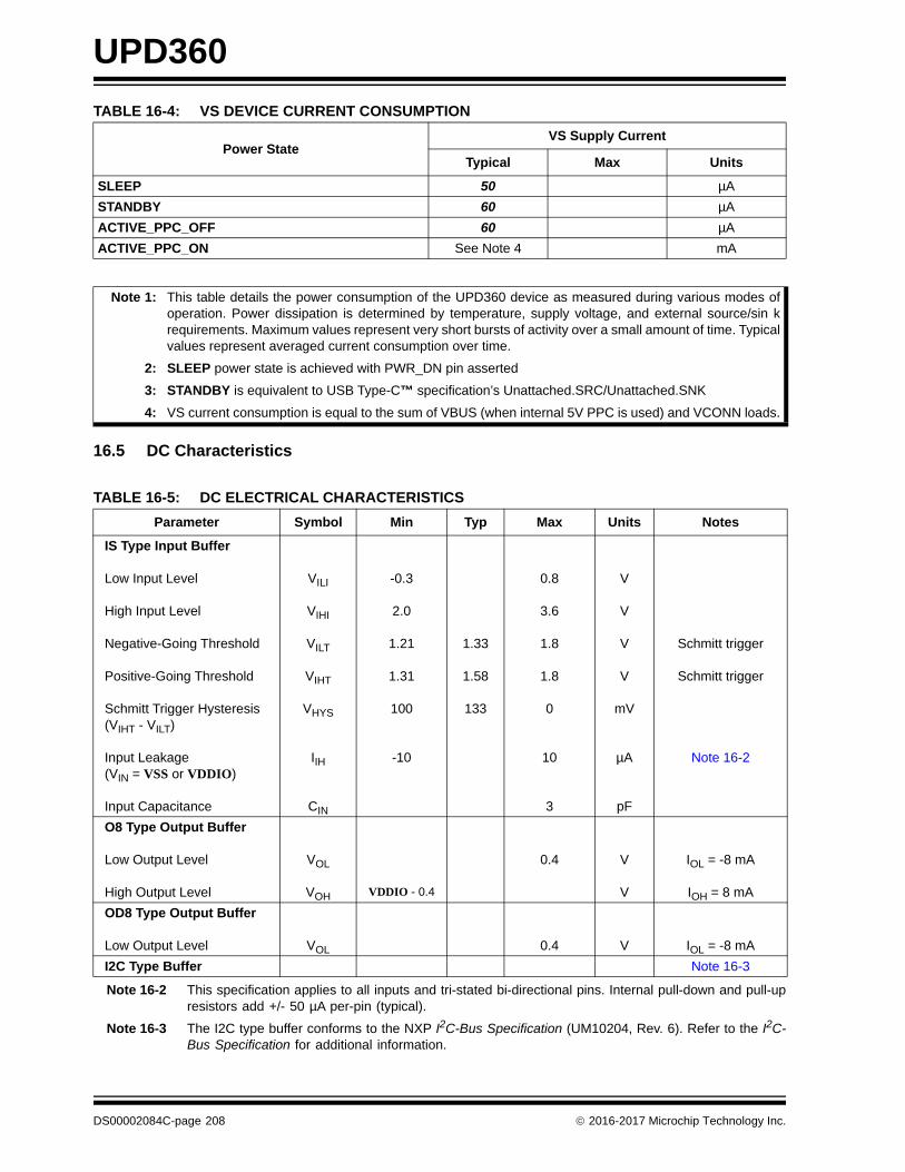
UPD360
TABLE 16-4: VS DEVICE CURRENT CONSUMPTION
16.5 DC Characteristics
Note 16-2 This specification applies to all inputs and tri-stated bi-directional pins. Internal pull-down and pull-upresistors add +/- 50 µA per-pin (typical).
Note 16-3 The I2C type buffer conforms to the NXP I2C-Bus Specification (UM10204, Rev. 6). Refer to the I2C-Bus Specification for additional information.
Power StateVS Supply Current
Typical Max Units
SLEEP 50 µA
STANDBY 60 µA
ACTIVE_PPC_OFF 60 µA
ACTIVE_PPC_ON See Note 4 mA
Note 1: This table details the power consumption of the UPD360 device as measured during various modes ofoperation. Power dissipation is determined by temperature, supply voltage, and external source/sin krequirements. Maximum values represent very short bursts of activity over a small amount of time. Typicalvalues represent averaged current consumption over time.
2: SLEEP power state is achieved with PWR_DN pin asserted
3: STANDBY is equivalent to USB Type-C™ specification’s Unattached.SRC/Unattached.SNK
4: VS current consumption is equal to the sum of VBUS (when internal 5V PPC is used) and VCONN loads.
TABLE 16-5: DC ELECTRICAL CHARACTERISTICS
Parameter Symbol Min Typ Max Units Notes
IS Type Input Buffer
Low Input Level
High Input Level
Negative-Going Threshold
Positive-Going Threshold
Schmitt Trigger Hysteresis (VIHT - VILT)
Input Leakage(VIN = VSS or VDDIO)
Input Capacitance
VILI
VIHI
VILT
VIHT
VHYS
IIH
CIN
-0.3
2.0
1.21
1.31
100
-10
1.33
1.58
133
0.8
3.6
1.8
1.8
0
10
3
V
V
V
V
mV
µA
pF
Schmitt trigger
Schmitt trigger
Note 16-2
O8 Type Output Buffer
Low Output Level
High Output Level
VOL
VOH VDDIO - 0.4
0.4 V
V
IOL = -8 mA
IOH = 8 mA
OD8 Type Output Buffer
Low Output Level VOL 0.4 V IOL = -8 mA
I2C Type Buffer Note 16-3
DS00002084C-page 208 2016-2017 Microchip Technology Inc.
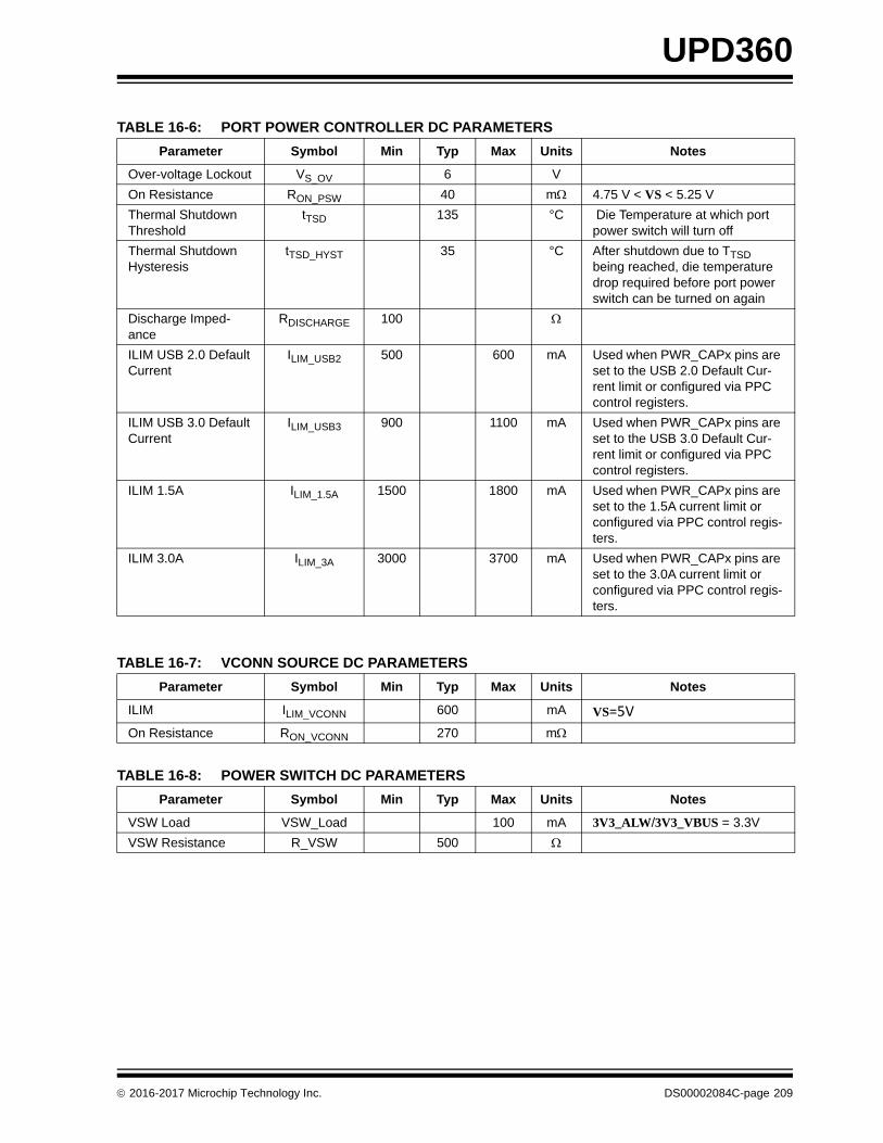
UPD360
TABLE 16-7: VCONN SOURCE DC PARAMETERS
TABLE 16-6: PORT POWER CONTROLLER DC PARAMETERS
Parameter Symbol Min Typ Max Units Notes
Over-voltage Lockout VS_OV 6 V
On Resistance RON_PSW 40 m 4.75 V < VS < 5.25 V
Thermal Shutdown Threshold
tTSD 135 °C Die Temperature at which port power switch will turn off
Thermal Shutdown Hysteresis
tTSD_HYST 35 °C After shutdown due to TTSD being reached, die temperature drop required before port power switch can be turned on again
Discharge Imped-ance
RDISCHARGE 100
ILIM USB 2.0 Default Current
ILIM_USB2 500 600 mA Used when PWR_CAPx pins are set to the USB 2.0 Default Cur-rent limit or configured via PPC control registers.
ILIM USB 3.0 Default Current
ILIM_USB3 900 1100 mA Used when PWR_CAPx pins are set to the USB 3.0 Default Cur-rent limit or configured via PPC control registers.
ILIM 1.5A ILIM_1.5A 1500 1800 mA Used when PWR_CAPx pins are set to the 1.5A current limit or configured via PPC control regis-ters.
ILIM 3.0A ILIM_3A 3000 3700 mA Used when PWR_CAPx pins are set to the 3.0A current limit or configured via PPC control regis-ters.
Parameter Symbol Min Typ Max Units Notes
ILIM ILIM_VCONN 600 mA VS=5V
On Resistance RON_VCONN 270 m
TABLE 16-8: POWER SWITCH DC PARAMETERS
Parameter Symbol Min Typ Max Units Notes
VSW Load VSW_Load 100 mA 3V3_ALW/3V3_VBUS = 3.3V
VSW Resistance R_VSW 500
2016-2017 Microchip Technology Inc. DS00002084C-page 209

UPD360
16.6 AC Characteristics and Timing
This section details the various AC timing specifications of the device.
16.6.1 RESET_N TIMING
Figure 16-2 illustrates the RESET_N timing requirements. Assertion of RESET_N is not a requirement. However, if used,it must be asserted for the minimum period specified
16.6.2 I2C SLAVE INTERFACE (UPD360-A/UPD360-B ONLY)
Figure 16-3 illustrates the I2C slave interface timing requirements. The I2C slave interface can operate in StandardMode, Fast Mode, or Fast Mode Plus. Refer to Section 5.0, "I2C Slave Controller (UPD360-A/UPD360-B Only)," onpage 20 for additional information.
FIGURE 16-2: RESET_N TIMING
TABLE 16-9: RESET_N TIMING VALUES
Symbol Description Min Typ Max Units
trstia RESET_N input assertion time 1 s
FIGURE 16-3: I2C SLAVE TIMING
RESET_N
trstia
bit 0(R/W)
I2C_CLK
I2C_DAT
Protocol
tBUF
tSU;STA
tHD;STA
tLOW
tHD;DAT
trtf
tHIGH 1 / fCLK
tSU;DAT
0.7 x VDD
0.3 x VDD
0.7 x VDD
0.3 x VDD
tVD;DAT tVD;ACK tSU;STO
START condition
(S)
bit 7MSB(A7)
acknowledge(A)
STOP(P)
bit 6(A6)
DS00002084C-page 210 2016-2017 Microchip Technology Inc.
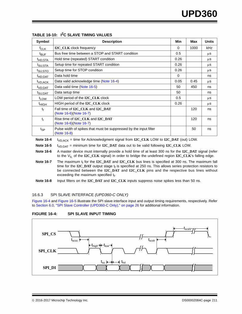
UPD360
Note 16-4 tVD;ACK = time for Acknowledgment signal from I2C_CLK LOW to I2C_DAT (out) LOW.
Note 16-5 tVD;DAT = minimum time for I2C_DAT data out to be valid following I2C_CLK LOW.
Note 16-6 A master device must internally provide a hold time of at least 300 ns for the I2C_DAT signal (referto the VIL of the I2C_CLK signal) in order to bridge the undefined region I2C_CLK‘s falling edge.
Note 16-7 The maximum tf for the I2C_DAT and I2C_CLK bus lines is specified at 300 ns. The maximum falltime for the I2C_DAT output stage tf is specified at 250 ns. This allows series protection resistors tobe connected between the I2C_DAT and I2C_CLK pins and the respective bus lines withoutexceeding the maximum specified tf.
Note 16-8 Input filters on the I2C_DAT and I2C_CLK inputs suppress noise spikes less than 50 ns.
16.6.3 SPI SLAVE INTERFACE (UPD360-C ONLY)
Figure 16-4 and Figure 16-5 illustrate the SPI slave interface input and output timing requirements, respectively. Referto Section 6.0, "SPI Slave Controller (UPD360-C Only)," on page 26 for additional information.
TABLE 16-10: I2C SLAVE TIMING VALUES
Symbol Description Min Max Units
fCLK I2C_CLK clock frequency 0 1000 kHz
tBUF Bus free time between a STOP and START condition 0.5 s
tHD;STA Hold time (repeated) START condition 0.26 s
tSU;STA Setup time for repeated START condition 0.26 s
tSU;STO Setup time for STOP condition 0.26 s
tHD;DAT Data hold time 0 ns
tVD;ACK Data valid acknowledge time (Note 16-4) 0.05 0.45 s
tVD;DAT Data valid time (Note 16-5) 50 450 ns
tSU;DAT Data setup time 50 ns
tLOW LOW period of the I2C_CLK clock 0.5 s
tHIGH HIGH period of the I2C_CLK clock 0.26 s
tf Fall time of I2C_CLK and I2C_DAT(Note 16-6)(Note 16-7)
120 ns
tr Rise time of I2C_CLK and I2C_DAT(Note 16-6)(Note 16-7)
120 ns
tSP Pulse width of spikes that must be suppressed by the input filter (Note 16-8)
50 ns
FIGURE 16-4: SPI SLAVE INPUT TIMING
SPI_CLK
SPI_DI
SPI_CStscss
thigh tlow
tsu thd
tscshl
tscsh
2016-2017 Microchip Technology Inc. DS00002084C-page 211

UPD360
Note 16-9 8.5 or 8.0, depending on loading of 30pF or 10pF, respectively.
16.6.4 PORT POWER CONTROLLER AC PARAMETERS
FIGURE 16-5: SPI SLAVE OUTPUT TIMING
TABLE 16-11: SPI TIMING VALUES
Symbol Description Min Typ Max Units
fsck SPI_CLK clock frequency 25 MHz
tclk_duty SPI_CLK high/low duty cycle 40 60 %
tscss SPI_CS setup time to SPI_CLK 5 ns
tscsh SPI_CS hold time from SPI_CLK 5 ns
tscshl SPI_CS inactive time 100 ns
tsu Data input setup time to SPI_CLK 10 ns
thd Data input hold time from SPI_CLK 4 ns
ton Data output turn on time from SPI_CLK 0 ns
tv Data output valid time from SPI_CLK Note 16-9 ns
tho Data output hold time from SPI_CLK 0 ns
tdis Data output disable time from SPI_CS inactive 20 ns
TABLE 16-12: PORT POWER CONTROLLER AC PARAMETERS
Parameter Symbol Min Typ Max Units Notes
Turn On Delay tON_PSW 0.75 ms PWR_EN active toggle to switch on time, VBUS discharge not active.
Turn Off Time tOFF_PSW_INA 0.75 ms PWR_EN inactive toggle to switch off time.CBUS = 120 F
Turn Off Time tOFF_PSW_ERR 1 ms Over-current Error, VBUS Min Error, or Discharge Error to switch off.CBUS = 120 F
Note 16-10
Turn Off Time tOFF_PSW_ERR 100 ns TSD or Back-drive Error to switch off.CBUS = 120 F
VBUS Output Rise Time
tR_BUS 1.1 ms Measured from 10% to 90% of VBUS, CLOAD = 220 FILIM = 1.0 A
Soft Turn on Rate IBUS / t 100 mA / µs
SPI_DO
SPI_CLKtclk_duty
SPI_CS
tdiston
tvtho
DS00002084C-page 212 2016-2017 Microchip Technology Inc.
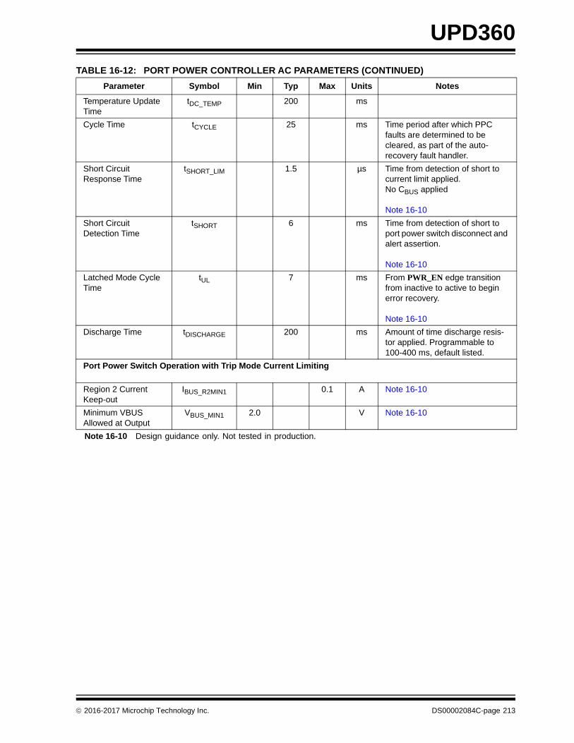
UPD360
Note 16-10 Design guidance only. Not tested in production.
Temperature Update Time
tDC_TEMP 200 ms
Cycle Time tCYCLE 25 ms Time period after which PPC faults are determined to be cleared, as part of the auto-recovery fault handler.
Short Circuit Response Time
tSHORT_LIM 1.5 µs Time from detection of short to current limit applied.No CBUS applied
Note 16-10
Short Circuit Detection Time
tSHORT 6 ms Time from detection of short to port power switch disconnect and alert assertion.
Note 16-10
Latched Mode Cycle Time
tUL 7 ms From PWR_EN edge transition from inactive to active to begin error recovery.
Note 16-10
Discharge Time tDISCHARGE 200 ms Amount of time discharge resis-tor applied. Programmable to 100-400 ms, default listed.
Port Power Switch Operation with Trip Mode Current Limiting
Region 2 Current Keep-out
IBUS_R2MIN1 0.1 A Note 16-10
Minimum VBUS Allowed at Output
VBUS_MIN1 2.0 V Note 16-10
TABLE 16-12: PORT POWER CONTROLLER AC PARAMETERS (CONTINUED)
Parameter Symbol Min Typ Max Units Notes
2016-2017 Microchip Technology Inc. DS00002084C-page 213

UPD360
17.0 PACKAGE INFORMATION
Note: For the most current package drawings, please see the Microchip Packaging Specification located at http://www.microchip.com/packaging
FIGURE 17-1: PACKAGE MARKING INFORMATION
44-WFBGA
UP360A
<V><COO>YWWNNN
3e <R>010
Legend: <R> Functional revision000 Firmware/Tracking number<V> Assembly vendor code<COO> Country codeY Year code (last 2 digits of calendar year)WW Week code (week of January 1 is week ‘01’)NNN Alphanumeric traceability code Pb-free JEDEC designator for Matte Tin (Sn)* This package is Pb-free. The Pb-free JEDEC designator ( )
can be found on the outer packaging for this package.
3e
3e
DS00002084C-page 214 2016-2017 Microchip Technology Inc.

UPD360
FIGURE 17-2: PACKAGE (DRAWING & DIMENSIONS)
2016-2017 Microchip Technology Inc. DS00002084C-page 215

UPD360
FIGURE 17-3: PACKAGE (BALL MATRIX & ROUTING)
DS00002084C-page 216 2016-2017 Microchip Technology Inc.
2016-2017 Microchip Technology Inc. DS00002084C-page 217
UPD360
APPENDIX A: DATA SHEET REVISION HISTORY
TABLE A-1: REVISION HISTORY
Revision Section/Figure/Entry Correction
DS00002084C (07-19-17) Public Release

UPD360
DS00002084C-page 218 2016-2017 Microchip Technology Inc.
THE MICROCHIP WEB SITE
Microchip provides online support via our WWW site at www.microchip.com. This web site is used as a means to makefiles and information easily available to customers. Accessible by using your favorite Internet browser, the web site con-tains the following information:
• Product Support – Data sheets and errata, application notes and sample programs, design resources, user’s guides and hardware support documents, latest software releases and archived software
• General Technical Support – Frequently Asked Questions (FAQ), technical support requests, online discussion groups, Microchip consultant program member listing
• Business of Microchip – Product selector and ordering guides, latest Microchip press releases, listing of semi-nars and events, listings of Microchip sales offices, distributors and factory representatives
CUSTOMER CHANGE NOTIFICATION SERVICE
Microchip’s customer notification service helps keep customers current on Microchip products. Subscribers will receivee-mail notification whenever there are changes, updates, revisions or errata related to a specified product family ordevelopment tool of interest.
To register, access the Microchip web site at www.microchip.com. Under “Support”, click on “Customer Change Notifi-cation” and follow the registration instructions.
CUSTOMER SUPPORT
Users of Microchip products can receive assistance through several channels:
• Distributor or Representative
• Local Sales Office
• Field Application Engineer (FAE)
• Technical Support
Customers should contact their distributor, representative or field application engineer (FAE) for support. Local salesoffices are also available to help customers. A listing of sales offices and locations is included in the back of this docu-ment.
Technical support is available through the web site at: http://www.microchip.com/support

2016-2017 Microchip Technology Inc. DS00002084C-page 219
UPD360
PRODUCT IDENTIFICATION SYSTEM
To order or obtain information, e.g., on pricing or delivery, refer to the factory or the listed sales office.
Device: UPD360
Tape and Reel Option:
Blank = Standard packaging (tray)T = Tape and Reel (Note 1)
Version: A = +1.8V I2C InterfaceB = +3.3V I2C InterfaceC = SPI Interface
Temperature Range:
Blank = 0C to +70C (Commercial)
Package: 6HX = 44-ball WFBGA
Examples:
a) UPD360-A/6HX+1.8V I2C Interface,Standard packaging,Commercial temperature,44-ball WFBGA package
b) UPD360T-B/6HX +3.3V I2C Interface,Tape and Reel,Commercial temperature,44-ball WFBGA package
c) UPD360-C/6HX SPI Interface,Standard packaging,Commercial temperature,44-ball WFBGA package
Note 1: Tape and Reel identifier only appears in the catalog part number description. This identifier is used for ordering purposes and is not printed on the device package. Check with your Microchip Sales Office for package availability with the Tape and Reel option.
PART NO. [X] /XXX
PackageTemp.Device
[X]( 1)
Tape & ReelOption Range
-X
Version

UPD360
DS
Note the following details of the code protection feature on Microchip devices:
• Microchip products meet the specification contained in their particular Microchip Data Sheet.
• Microchip believes that its family of products is one of the most secure families of its kind on the market today, when used in the intended manner and under normal conditions.
• There are dishonest and possibly illegal methods used to breach the code protection feature. All of these methods, to our knowledge, require using the Microchip products in a manner outside the operating specifications contained in Microchip’s Data Sheets. Most likely, the person doing so is engaged in theft of intellectual property.
• Microchip is willing to work with the customer who is concerned about the integrity of their code.
• Neither Microchip nor any other semiconductor manufacturer can guarantee the security of their code. Code protection does not mean that we are guaranteeing the product as “unbreakable.”
Code protection is constantly evolving. We at Microchip are committed to continuously improving the code protection features of ourproducts. Attempts to break Microchip’s code protection feature may be a violation of the Digital Millennium Copyright Act. If such actsallow unauthorized access to your software or other copyrighted work, you may have a right to sue for relief under that Act.
Information contained in this publication regarding device applications and the like is provided only for your convenience and may besuperseded by updates. It is your responsibility to ensure that your application meets with your specifications. MICROCHIP MAKES NOREPRESENTATIONS OR WARRANTIES OF ANY KIND WHETHER EXPRESS OR IMPLIED, WRITTEN OR ORAL, STATUTORY OROTHERWISE, RELATED TO THE INFORMATION, INCLUDING BUT NOT LIMITED TO ITS CONDITION, QUALITY, PERFORMANCE,MERCHANTABILITY OR FITNESS FOR PURPOSE. Microchip disclaims all liability arising from this information and its use. Use of Micro-chip devices in life support and/or safety applications is entirely at the buyer’s risk, and the buyer agrees to defend, indemnify and holdharmless Microchip from any and all damages, claims, suits, or expenses resulting from such use. No licenses are conveyed, implicitly orotherwise, under any Microchip intellectual property rights unless otherwise stated.
Trademarks
The Microchip name and logo, the Microchip logo, AnyRate, AVR, AVR logo, AVR Freaks, BeaconThings, BitCloud, CryptoMemory, CryptoRF, dsPIC, FlashFlex, flexPWR, Heldo, JukeBlox, KEELOQ, KEELOQ logo, Kleer, LANCheck, LINK MD, maXStylus, maXTouch, MediaLB, megaAVR, MOST, MOST logo, MPLAB, OptoLyzer, PIC, picoPower, PICSTART, PIC32 logo, Prochip Designer, QTouch, RightTouch, SAM-BA, SpyNIC, SST, SST Logo, SuperFlash, tinyAVR, UNI/O, and XMEGA are registered trademarks of Microchip Technology Incorporated in the U.S.A. and other countries.
ClockWorks, The Embedded Control Solutions Company, EtherSynch, Hyper Speed Control, HyperLight Load, IntelliMOS, mTouch, Precision Edge, and Quiet-Wire are registered trademarks of Microchip Technology Incorporated in the U.S.A.
Adjacent Key Suppression, AKS, Analog-for-the-Digital Age, Any Capacitor, AnyIn, AnyOut, BodyCom, chipKIT, chipKIT logo, CodeGuard, CryptoAuthentication, CryptoCompanion, CryptoController, dsPICDEM, dsPICDEM.net, Dynamic Average Matching, DAM, ECAN, EtherGREEN, In-Circuit Serial Programming, ICSP, Inter-Chip Connectivity, JitterBlocker, KleerNet, KleerNet logo, Mindi, MiWi, motorBench, MPASM, MPF, MPLAB Certified logo, MPLIB, MPLINK, MultiTRAK, NetDetach, Omniscient Code Generation, PICDEM, PICDEM.net, PICkit, PICtail, PureSilicon, QMatrix, RightTouch logo, REAL ICE, Ripple Blocker, SAM-ICE, Serial Quad I/O, SMART-I.S., SQI, SuperSwitcher, SuperSwitcher II, Total Endurance, TSHARC, USBCheck, VariSense, ViewSpan, WiperLock, Wireless DNA, and ZENA are trademarks of Microchip Technology Incorporated in the U.S.A. and other countries.
SQTP is a service mark of Microchip Technology Incorporated in the U.S.A.
Silicon Storage Technology is a registered trademark of Microchip Technology Inc. in other countries.
GestIC is a registered trademark of Microchip Technology Germany II GmbH & Co. KG, a subsidiary of Microchip Technology Inc., in other countries.
All other trademarks mentioned herein are property of their respective companies.
© 2016-2017, Microchip Technology Incorporated, All Rights Reserved.
ISBN: 9781522419181
00002084C-page 220 2016-2017 Microchip Technology Inc.
Microchip received ISO/TS-16949:2009 certification for its worldwide headquarters, design and wafer fabrication facilities in Chandler and Tempe, Arizona; Gresham, Oregon and design centers in California and India. The Company’s quality system processes and procedures are for its PIC® MCUs and dsPIC® DSCs, KEELOQ® code hopping devices, Serial EEPROMs, microperipherals, nonvolatile memory and analog products. In addition, Microchip’s quality system for the design and manufacture of development systems is ISO 9001:2000 certified.
QUALITYMANAGEMENTSYSTEMCERTIFIEDBYDNV
== ISO/TS16949==

DS00002084C-page 221 2016-2017 Microchip Technology Inc.
AMERICASCorporate Office2355 West Chandler Blvd.Chandler, AZ 85224-6199Tel: 480-792-7200 Fax: 480-792-7277Technical Support: http://www.microchip.com/supportWeb Address: www.microchip.com
AtlantaDuluth, GA Tel: 678-957-9614 Fax: 678-957-1455
Austin, TXTel: 512-257-3370
BostonWestborough, MA Tel: 774-760-0087 Fax: 774-760-0088
ChicagoItasca, IL Tel: 630-285-0071 Fax: 630-285-0075
DallasAddison, TX Tel: 972-818-7423 Fax: 972-818-2924
DetroitNovi, MI Tel: 248-848-4000
Houston, TX Tel: 281-894-5983
IndianapolisNoblesville, IN Tel: 317-773-8323Fax: 317-773-5453Tel: 317-536-2380
Los AngelesMission Viejo, CA Tel: 949-462-9523Fax: 949-462-9608Tel: 951-273-7800
Raleigh, NC Tel: 919-844-7510
New York, NY Tel: 631-435-6000
San Jose, CA Tel: 408-735-9110Tel: 408-436-4270
Canada - TorontoTel: 905-695-1980 Fax: 905-695-2078
ASIA/PACIFICAsia Pacific OfficeSuites 3707-14, 37th FloorTower 6, The GatewayHarbour City, Kowloon
Hong KongTel: 852-2943-5100Fax: 852-2401-3431
Australia - SydneyTel: 61-2-9868-6733Fax: 61-2-9868-6755
China - BeijingTel: 86-10-8569-7000 Fax: 86-10-8528-2104
China - ChengduTel: 86-28-8665-5511Fax: 86-28-8665-7889
China - ChongqingTel: 86-23-8980-9588Fax: 86-23-8980-9500
China - DongguanTel: 86-769-8702-9880
China - GuangzhouTel: 86-20-8755-8029
China - HangzhouTel: 86-571-8792-8115 Fax: 86-571-8792-8116
China - Hong Kong SARTel: 852-2943-5100 Fax: 852-2401-3431
China - NanjingTel: 86-25-8473-2460Fax: 86-25-8473-2470
China - QingdaoTel: 86-532-8502-7355Fax: 86-532-8502-7205
China - ShanghaiTel: 86-21-3326-8000 Fax: 86-21-3326-8021
China - ShenyangTel: 86-24-2334-2829Fax: 86-24-2334-2393
China - ShenzhenTel: 86-755-8864-2200 Fax: 86-755-8203-1760
China - WuhanTel: 86-27-5980-5300Fax: 86-27-5980-5118
China - XianTel: 86-29-8833-7252Fax: 86-29-8833-7256
ASIA/PACIFICChina - XiamenTel: 86-592-2388138 Fax: 86-592-2388130
China - ZhuhaiTel: 86-756-3210040 Fax: 86-756-3210049
India - BangaloreTel: 91-80-3090-4444 Fax: 91-80-3090-4123
India - New DelhiTel: 91-11-4160-8631Fax: 91-11-4160-8632
India - PuneTel: 91-20-3019-1500
Japan - OsakaTel: 81-6-6152-7160 Fax: 81-6-6152-9310
Japan - TokyoTel: 81-3-6880- 3770 Fax: 81-3-6880-3771
Korea - DaeguTel: 82-53-744-4301Fax: 82-53-744-4302
Korea - SeoulTel: 82-2-554-7200Fax: 82-2-558-5932 or 82-2-558-5934
Malaysia - Kuala LumpurTel: 60-3-6201-9857Fax: 60-3-6201-9859
Malaysia - PenangTel: 60-4-227-8870Fax: 60-4-227-4068
Philippines - ManilaTel: 63-2-634-9065Fax: 63-2-634-9069
SingaporeTel: 65-6334-8870Fax: 65-6334-8850
Taiwan - Hsin ChuTel: 886-3-5778-366Fax: 886-3-5770-955
Taiwan - KaohsiungTel: 886-7-213-7830
Taiwan - TaipeiTel: 886-2-2508-8600 Fax: 886-2-2508-0102
Thailand - BangkokTel: 66-2-694-1351Fax: 66-2-694-1350
EUROPEAustria - WelsTel: 43-7242-2244-39Fax: 43-7242-2244-393
Denmark - CopenhagenTel: 45-4450-2828 Fax: 45-4485-2829
Finland - EspooTel: 358-9-4520-820
France - ParisTel: 33-1-69-53-63-20 Fax: 33-1-69-30-90-79
France - Saint CloudTel: 33-1-30-60-70-00
Germany - GarchingTel: 49-8931-9700Germany - HaanTel: 49-2129-3766400
Germany - HeilbronnTel: 49-7131-67-3636
Germany - KarlsruheTel: 49-721-625370
Germany - MunichTel: 49-89-627-144-0 Fax: 49-89-627-144-44
Germany - RosenheimTel: 49-8031-354-560
Israel - Ra’anana Tel: 972-9-744-7705
Italy - Milan Tel: 39-0331-742611 Fax: 39-0331-466781
Italy - PadovaTel: 39-049-7625286
Netherlands - DrunenTel: 31-416-690399 Fax: 31-416-690340
Norway - TrondheimTel: 47-7289-7561
Poland - WarsawTel: 48-22-3325737
Romania - BucharestTel: 40-21-407-87-50
Spain - MadridTel: 34-91-708-08-90Fax: 34-91-708-08-91
Sweden - GothenbergTel: 46-31-704-60-40
Sweden - StockholmTel: 46-8-5090-4654
UK - WokinghamTel: 44-118-921-5800Fax: 44-118-921-5820
Worldwide Sales and Service
11/07/16