usage as buffer for homo- and heteroepitaxial overgrowth...
TRANSCRIPT

Subscriber access provided by INSTITUTE OF PHYSICS
Langmuir is published by the American Chemical Society. 1155 Sixteenth Street N.W.,Washington, DC 20036
Article
Subnanometer-Thick PbS Film on Organic Substrate and ItsUsage as Buffer for Homo- and Heteroepitaxial Overgrowth
Yu-Dong Zhang, Shu-Xin Hu, Bing Yuan, Xi-Miao Hou, Ying Lu, and Ming LiLangmuir, 2009, 25 (10), 5609-5613• DOI: 10.1021/la804295p • Publication Date (Web): 05 March 2009
Downloaded from http://pubs.acs.org on May 14, 2009
More About This Article
Additional resources and features associated with this article are available within the HTML version:
• Supporting Information• Access to high resolution figures• Links to articles and content related to this article• Copyright permission to reproduce figures and/or text from this article

pubs.acs.org/Langmuir
Subnanometer-Thick PbSFilm onOrganic Substrate and ItsUsage as Buffer
for Homo- and Heteroepitaxial Overgrowth
Yu-Dong Zhang, Shu-Xin Hu,* Bing Yuan, Xi-Miao Hou, Ying Lu, and Ming Li
Beijing National Laboratory for Condensed Matter Physics, Institute of Physics, Chinese Academy ofSciences, Beijing 100190, China
Received December 29, 2008. Revised Manuscript Received February 11, 2009
We report on the fabrication of a subnanometer-thick epitaxial PbS film on polydiacetylene (PDA) substrate.The film is formed by cation-absorption in PbCl2 solution followed by sulfidation in mixed H2S/N2 gas,exhibiting a flat and smooth surface morphology. The strong adsorbate-surface interaction between the leadhydrolysis complexes and the carboxyl headgroups on the surface of PDA accounts for such a growth mode.Wefurther demonstrate that such an ultrathin film can be used as a buffer layer for both homo- and heteroepitaxialgrowth of sulfide films. The X-ray and electron diffraction results reveal that the (001) planes of PbS are parallelto the surface of PDA and the (110) planes of PbS are parallel to the (110) planes of PDA.
Introduction
Organic-inorganic hybrid materials have gained muchattention because of their potential applications in opticsand electronics.1-5 Fabrication of the hybrids often involvesgrowthof organic components on inorganic surfaces, and viceversa. Highly ordered organic thin films on inorganic sub-strates can be obtained using amphiphilic molecules, oftenrealized bymeans of LB technique, self-assemblymethod, andso on.6,7 However, the growth of inorganic materials onorganic substrates, which is common in nature, is still challen-ging in material engineering.8,9 Inorganic thin films are oftengrown with sophisticated, high-cost physical techniques re-quiring high temperature and high vacuum, which may bringserious damage to the organic components and hence are notapplicable to the fabricationof hybridmaterials.10Techniquesinvolving mild conditions andmoderate temperatures such aschemical bath deposition (CBD),11 successive ionic adsorp-tion and reaction (SILAR),12 or ion layer gas reaction(ILGAR),13 however, often lead to polycrystalline thin filmsgrown in islandlike mode. Layerlike growth mode is essentialto obtain crystalline films, while islandlike growthmode oftenresults in clusters. The competition between the two growth
modes depends on the competition between the adsorbate-substrate and the adsorbate-adsorbate interactions.10 In lightof such thought, it is of fundamental and practical interest toask if one canmaximize the adsorbate-substrate interactionsto realize the layerlike growth mode and, ultimately, tofabricate epitaxial inorganic thin films on organic substrates.
Herein, we show that a subnanometer-thick PbS film can beexpitaxially grown on polydiacetylene (PDA) substrates. Wefurther demonstrate that such an ultrathin film can act as abuffer layer for both homogeneous and heterogeneous over-growth of sulfide films. The film is formed by cation-absorp-tion in PbCl2 solution followed by sulfidation in mixed H2S/N2 gas. The technique is similar to the ILGAR.14,15 However,it differs from ILGAR by a strict rinsing process beforesulfidation to make sure that only the most tightly absorbedcations remainon the surface,which is essential to the layerlikegrowth mode and the flat and smooth surface morphology.
Experimental Section
Chemicals. The monomer of PDA, 10,12-tricosadiynoic acid(TCDA, CH3(CH2)9CtC;CtC (CH2)8COOH), g98.0%),was purchased from Fluka and recrystallized with petroleumether before use. All other organic and inorganic reagents(from the Beijing Chemical Reagents Company) were analyticalreagent grade and were used as received. Distilled water (>18.2MΩ) was produced using a Millipore filter system.
Preparation of the Organic Substrates. TCDA thin filmswerepreparedonSi(001)wafers usingadrop-castingmethod.16-18
Briefly, TCDA was dissolved in acetonitrile (2 mmol/L) andpipetted onto the hydrophilic silicon surface (10 � 10 mm2). Thesample was then moved into a chamber with controlled tempera-ture (∼50 �C) and relative humidity (∼90% RH). As the solventevaporated slowly, a white film of TCDA was obtained. The film
*To whom correspondence should be addressed. E-mail: [email protected]. Fax: (+86) 10-82640224.
(1) Mitzi, D.; Chondroudis, K.; Kagan, C. IBM J. Res. & Dev. 2001, 45,29.
(2) Sanchez, C.; Julian, B.; Belleville, P.; Popall, M. J.Mater. Chem. 2005,15, 3559.
(3) Wang, L.; Yoon, M.; Lu, G.; Yang, Y.; Facchetti, A.; Marks, T. Nat.Mater. 2006, 5, 893.
(4) Lee, B. H.; Ryu, M. K.; Choi, S.; Lee, K.; Im, S.; Sung, M. M. J. Am.Chem. Soc. 2007, 129, 16034.
(5) Wang, L.; Yoon,M.; Facchetti, A.; Marks, T. J.Adv. Mater. 2007, 19,3252.
(6) Petty,M. C.Langmuir-Blodgett Film-An Introduction;CambridgeUni-versity Press: Cambridge, U.K., 1996.
(7) Ulman, A. An Introduction to Ultrathin Organic Films: From Lang-muir-Blodgett to Self-Assembly; Academic Press: Boston, 1991.
(8) Calvert, P.; Rieke, P. Chem. Mater. 1996, 8, 1715.(9) Ludwigs, S.; Steiner, U.; Kulak, A. N.; Lam, R.; Meldrum, F. C. Adv.
Mater. 2006, 18, 2270.(10) Gao, Y. F.; Koumoto, K. Cryst. Growth Des. 2005, 5, 1983.(11) Meldrum, F. C.; Flath, J.; Knoll, W. Langmuir 1997, 13, 2033.(12) Meldrum, F. C.; Flath, J.; Knoll, W. Thin Solid Films 1999, 348, 188.(13) Jiang, P.; Liu, Z.; Cai, S. Langmuir 2002, 18, 4495.
(14) Moller, J.; Fischer, C. H.; Muffler, H. J.; Konenkamp, R.; Kaiser, I.;Kelch, C.; Lux-Steiner, M. C. Thin Solid Films 2000, 361, 113.
(15) Muffler, H. J.; Fischer, C. H.; Giersig, M.; Bar, M.; Lux-Steiner, M.C. J. Appl. Phys. 2002, 91, 6691.
(16) Hu, S.; Li, X.; Jia, Q.; Mai, Z.; Li, M. J. Chem. Phys. 2005, 122,124712.
(17) Xing, L.; Li, D.; Hu, S.; Jing, H.; Fu, H.;Mai, Z.; Li,M. J. Am. Chem.Soc. 2006, 128, 1749.
(18) Yuan, B.; Xing, L.; Zhang, Y.; Lu, Y.; Mai, Z.; Li, M. J. Am. Chem.Soc. 2007, 129, 11332.
Published on Web 3/5/2009
© 2009 American Chemical Society
DOI: 10.1021/la804295pLangmuir 2009, 25(10), 5609–5613 5609

was then polymerized by radiation with UV light for 12 h. Theresulting polycrystalline PDA films (about 0.5 μm thick) in redphase were used as the organic substrates in this work. Before use,the PDA substrates were stored in water at 40 �C. A long soakingtime is essential to render the surface of PDA hydrophilic.
Growth of PbS Ultrathin Film. The PbS ultrathin film wasformed by cation-absorption in PbCl2 solution followed bysulfidation in H2S/N2 gas. The growth begins with immersingthe substrate with a hydrophilic surface in the PbCl2 solution(pH 5.5) for 1 h, followed by a careful rinsingwith distilled watertominimize the amount of lead ions on the surface. After dryingin air for 30 min, the sample was moved into a chamber filledwith a mixture of H2S and N2 (1:5, by volume) for sulfidation.Nitrogen was added to dilute the H2S so that the sulfudationreaction was mild.
Epitaxial Overgrowth of PbS and CdS. With the PbSultrathin film as the buffer layer, homogeneous PbS or hetero-geneous sulfide (CdS in our experiment) can be grown byrepeating the aforementioned immersing-rinsing-sulfidationprocess. The growth rate of thin films depends on the concentra-tion of the solutions and the rinsing strength. When the concen-tration of the PbCl2 solution is 0.01M, the growth rate is around4 A per cycle. To achieve a similar growth rate, a higherconcentration is required of the CdCl2 solution (pH ∼ 5.5) thanof the PbCl2 solution. When the concentration of the CdCl2solution is 0.1 M, the growth rate is around 3 A per cycle.
StructuralCharacterization. Surfacemorphologiesweremea-sured by using a Nanoscope IIIa atomic force microscope (AFM)(Digital Instruments, Santa Barbara, CA). All AFM images wereobtained in air at room temperature using tapping mode.
X-ray diffraction (XRD) measurements were performed on afive-circle Huber diffractometer on the 4W1A beam line at theBeijing Synchrotron Radiation Facility. The wavelength of theX-rays was 0.154 ( 0.001 nm. The vertical and horizontalangular divergences of the focused X-ray beam were 0.02� and0.08�, respectively. The grazing incidence X-ray diffraction(GIXRD) measurements were performed at the Diffractionand Scattering Station of the National Synchrotron RadiationLaboratory in Hefei. The sample was mounted horizontally onan eight-circle Huber diffractometer. The goniometer was care-fully aligned so that the incidence anglewas kept at 0.3�while thesample was rotating around its normal. A 330 mm diametercharge-coupled detector (Mar-Research) was used to collect thediffraction patterns.
ACM12 electronmicroscope operated at 100KVwas used forthe structural characterization. Specimens for transmission elec-tron microscopy (TEM) were prepared by scraping the layersfrom the substrates with a razor blade while the samples wereimmersed in deionized pure water. The rolled layers formed byscrapingwere flattened and floatedon thewater surface under thesurface tension. The flattened layer samples were then carefullytransferred to TEM copper grids for TEM observations. Toreduce the sample damage by electron irradiation, a low tem-perature sample stage cooled with liquid nitrogen was used andthe experiments were performed at 93 ( 1 K. The electrondiffraction (ED) pattern disappears in about 15 s under theelectron irradiation, and hence, quick operation is important.
Results and Discussion
The PDA substrate is made of 10,12-tricosadiynoic acid(TCDA) molecules, having a multilayered structure with aroot mean squared surface roughness of only 0.3 nm. (Thescheme of the TCDA molecule, the multilayered PDA sub-strate, the 2D lattice of PDA surface, the XRD and EDpatterns, and the AFM image of the PDA surface can all befound in the Supporting Information). After the immersing-rinsing-sulfidation process, an ultrathin PbS film is formedon the PDA substrate. The overgrown film does not affect the
structure of the substrate as can been seen from the compar-ison of the twoXRDpatterns before and after the film growth(Figure 1). The extra peak centered at about 2θ=30� in curveb is due to the (002) Bragg diffraction of the PbS film(according to the Powder Diffraction File data). Assumingthe film is homogeneous, we can derive a formula to calculatethe profile of the (002) peak. It reads as
I002� sind
2Δqz
� �=Δqz
��������2
ð1Þ
where d is the mean thickness of the ultrathin film andΔqz=(4π/λ)(sin θ - sin θ002) denotes the deviation from the Braggpeak with θ being the incident angle and θ002 the Bragg angle.The calculation showed that the mean thickness of the ultra-thin film is about 5 A, corresponding to about two PbS layers.(Detailed simulation is shown in Figure S4 in the SupportingInformation).
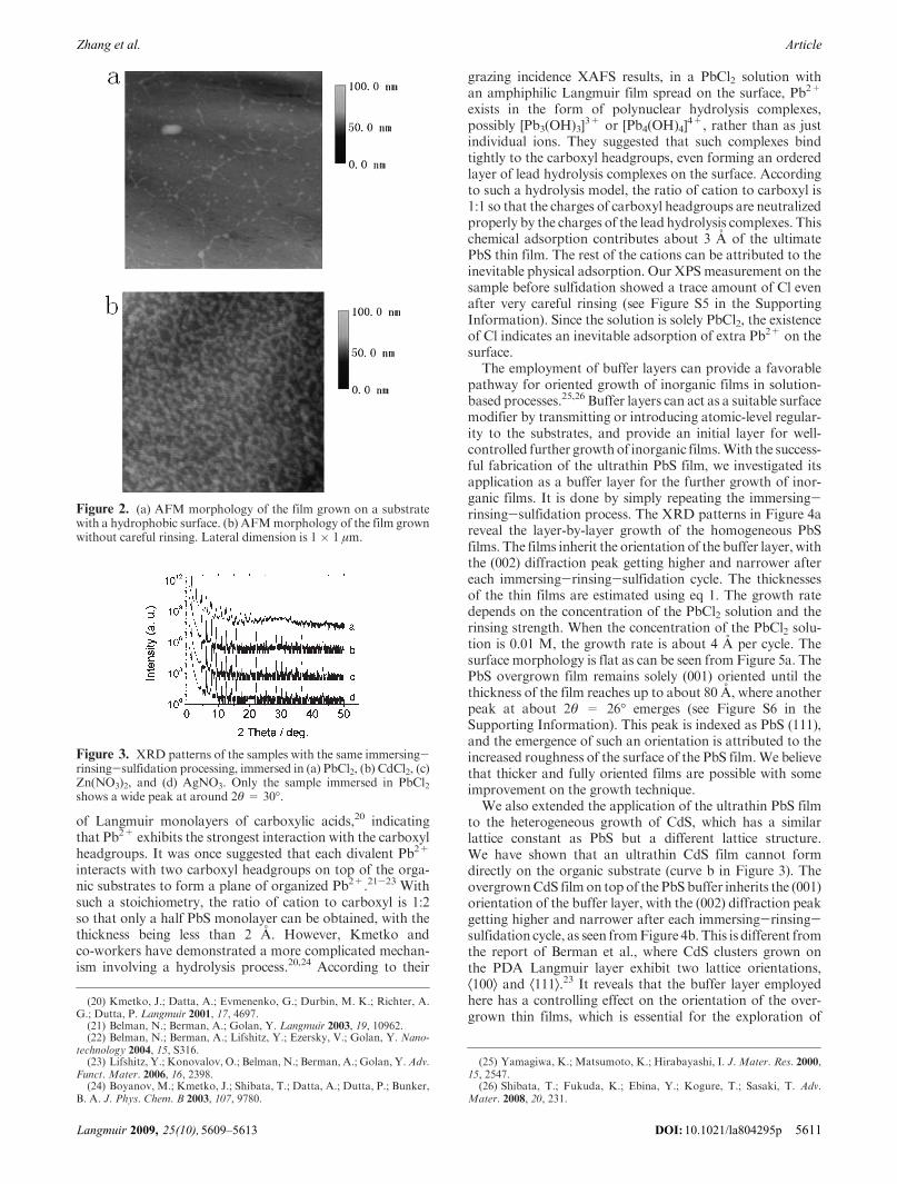
The AFM image in the inset of Figure 1 shows that thesurface of thePbS film is smoothwitha roughnessof about 0.6nm, only slightly rougher than the PDA surface. Such alayerlike growth mode was previously achieved only withcomplicated physical methods such as MBE.19 We believethat the strong adsorbate-substrate interaction between thePb2+ ions and the carboxyl headgroups on the surface ofPDA accounts for such a layerlike growth mode for thefollowing reasons. (1) Before use, the surface of the PDAsubstrate must be rendered hydrophilic with a surface contactangle smaller than 40� by storing in water for more than 20 hat 40 �C to remove the hydrophobic single layer and exposethe carboxyl groups to the cations. No cations can beabsorbed onto the surface if the surface is hydrophobic withthe methyl groups upward. Actually, the ultrathin PbS filmdoes not form on some less carefully prepared substrates(Figure 2a). (2) A careful rinsing process ensures that onlythemost tightly absorbed Pb2+ cations remain on the organicsubstrate before sulfidation. Without the rinsing process, thesurface of PDA will be covered with loosely deposited excesssalts which incline to form islands upon sulfidation owing tothe weak adsorbate-substrate interactions (Figure 2b).
Of the many metal ions (Cd2+, Zn2+, and Ag+) tested inour study, only Pb2+ can lead to such an ultrathin film on theorganic substrate. Figure 3 shows the XRD patterns of thesamples with the same immersing-rinsing-sulfidation pro-cess when immersed in PbCl2, CdCl2, Zn(NO3)2, andAgNO3.The observation is consistent with the fact that Pb2+ wassingled out to have the greatest influence on the structure
Figure 1. XRD pattern of the PDA substrate (a) and the sampleafter a cycle of the immersing-rinsing-sulfidation process (b). Awidepeakataround2θ=30� arises fromtheultrathinPbS film. Insetshows the AFM morphology of the PbS film on PDA.
(19) Preobrajenski, A. B.; Chasse, T. Appl. Surf. Sci. 1999, 142, 394.
DOI: 10.1021/la804295p Langmuir 2009, 25(10),5609–56135610
Article Zhang et al.
of Langmuir monolayers of carboxylic acids,20 indicatingthat Pb2+ exhibits the strongest interaction with the carboxylheadgroups. It was once suggested that each divalent Pb2+
interacts with two carboxyl headgroups on top of the orga-nic substrates to form a plane of organized Pb2+.21-23 Withsuch a stoichiometry, the ratio of cation to carboxyl is 1:2so that only a half PbS monolayer can be obtained, with thethickness being less than 2 A. However, Kmetko andco-workers have demonstrated a more complicated mechan-ism involving a hydrolysis process.20,24 According to their
grazing incidence XAFS results, in a PbCl2 solution withan amphiphilic Langmuir film spread on the surface, Pb2+
exists in the form of polynuclear hydrolysis complexes,possibly [Pb3(OH)3]
3+ or [Pb4(OH)4]4+, rather than as just
individual ions. They suggested that such complexes bindtightly to the carboxyl headgroups, even forming an orderedlayer of lead hydrolysis complexes on the surface. Accordingto such a hydrolysis model, the ratio of cation to carboxyl is1:1 so that the charges of carboxyl headgroups are neutralizedproperly by the charges of the lead hydrolysis complexes. Thischemical adsorption contributes about 3 A of the ultimatePbS thin film. The rest of the cations can be attributed to theinevitable physical adsorption. Our XPS measurement on thesample before sulfidation showed a trace amount of Cl evenafter very careful rinsing (see Figure S5 in the SupportingInformation). Since the solution is solely PbCl2, the existenceof Cl indicates an inevitable adsorption of extra Pb2+ on thesurface.
The employment of buffer layers can provide a favorablepathway for oriented growth of inorganic films in solution-based processes.25,26 Buffer layers can act as a suitable surfacemodifier by transmitting or introducing atomic-level regular-ity to the substrates, and provide an initial layer for well-controlled further growthof inorganic films.With the success-ful fabrication of the ultrathin PbS film, we investigated itsapplication as a buffer layer for the further growth of inor-ganic films. It is done by simply repeating the immersing-rinsing-sulfidation process. The XRD patterns in Figure 4areveal the layer-by-layer growth of the homogeneous PbSfilms. The films inherit the orientation of the buffer layer, withthe (002) diffraction peak getting higher and narrower aftereach immersing-rinsing-sulfidation cycle. The thicknessesof the thin films are estimated using eq 1. The growth ratedepends on the concentration of the PbCl2 solution and therinsing strength. When the concentration of the PbCl2 solu-tion is 0.01 M, the growth rate is about 4 A per cycle. Thesurface morphology is flat as can be seen from Figure 5a. ThePbS overgrown film remains solely (001) oriented until thethickness of the film reaches up to about 80 A, where anotherpeak at about 2θ = 26� emerges (see Figure S6 in theSupporting Information). This peak is indexed as PbS (111),and the emergence of such an orientation is attributed to theincreased roughness of the surface of the PbS film.We believethat thicker and fully oriented films are possible with someimprovement on the growth technique.
We also extended the application of the ultrathin PbS filmto the heterogeneous growth of CdS, which has a similarlattice constant as PbS but a different lattice structure.We have shown that an ultrathin CdS film cannot formdirectly on the organic substrate (curve b in Figure 3). TheovergrownCdS filmon top of the PbS buffer inherits the (001)orientation of the buffer layer, with the (002) diffraction peakgetting higher and narrower after each immersing-rinsing-sulfidation cycle, as seen fromFigure 4b. This is different fromthe report of Berman et al., where CdS clusters grown onthe PDA Langmuir layer exhibit two lattice orientations,Æ100æ and Æ111æ.23 It reveals that the buffer layer employedhere has a controlling effect on the orientation of the over-grown thin films, which is essential for the exploration of
Figure 2. (a) AFM morphology of the film grown on a substratewith a hydrophobic surface. (b) AFMmorphology of the film grownwithout careful rinsing. Lateral dimension is 1 � 1 μm.
Figure 3. XRD patterns of the samples with the same immersing-rinsing-sulfidation processing, immersed in (a) PbCl2, (b) CdCl2, (c)Zn(NO3)2, and (d) AgNO3. Only the sample immersed in PbCl2shows a wide peak at around 2θ = 30�.
(20) Kmetko, J.; Datta, A.; Evmenenko, G.; Durbin, M. K.; Richter, A.G.; Dutta, P. Langmuir 2001, 17, 4697.
(21) Belman, N.; Berman, A.; Golan, Y. Langmuir 2003, 19, 10962.(22) Belman, N.; Berman, A.; Lifshitz, Y.; Ezersky, V.; Golan, Y. Nano-
technology 2004, 15, S316.(23) Lifshitz, Y.; Konovalov, O.; Belman, N.; Berman, A.; Golan, Y.Adv.
Funct. Mater. 2006, 16, 2398.(24) Boyanov, M.; Kmetko, J.; Shibata, T.; Datta, A.; Dutta, P.; Bunker,
B. A. J. Phys. Chem. B 2003, 107, 9780.
(25) Yamagiwa, K.; Matsumoto, K.; Hirabayashi, I. J. Mater. Res. 2000,15, 2547.
(26) Shibata, T.; Fukuda, K.; Ebina, Y.; Kogure, T.; Sasaki, T. Adv.Mater. 2008, 20, 231.
DOI: 10.1021/la804295pLangmuir 2009, 25(10), 5609–5613 5611
ArticleZhang et al.

orientation-dependent properties.27 A higher CdCl2 concen-tration is required to achieve a similar growth rate. When theconcentration of the CdCl2 solution is 0.1 M, the growth rateis about 3 A per cycle. The surface morphology is also flat as
can be seen from Figure 5b. Therefore, the ultrathin PbS filmcan provide a favorable buffer layer for not only the homo-geneous growth of PbS films but also the heterogeneousgrowth of sulfide films.
We studied the epitaxial relationship between the lattices ofPbS and PDA using grazing incidence XRD (GIXRD) andED.Because the signals from the subnanometer-thick film arevery weak, we performed themeasurement on a PbS film afterseveral cycles of growth. The peaks in the GIXRD map(Figure 6) can be indexed according to the d-spacing of therelevant materials (based on the Powder Diffraction Filedata). First, the two strongest peaks are recognized to be Si(111) and (220), respectively. With these peaks’ positions as areference, we can index the rest of the peaks. The positions ofthese peaks are consistent with the results of Berman et al.’sGIXRD experiments.23 The PbS (111), (200), and (220) peaksare clearly visible, indicating that the PbS thin film is highlyoriented with its (001) planes parallel to the surface, confirm-ing the XRD results. The d-spacing of the PDA (110) planesand the PbS (110) planes is almost identical, about 4.3 A. Thestrain of the lattice is the least when the two sets of planes areparallel.We propose that such a lattice matching accounts forthe epitaxial growth of PbS on PDA, just as that reported byFendler co-workers in their pioneer work studying the epitax-ial growth of sulfides under Langmuir films.28,29
Figure 7 shows theEDpattern of the PbS film grown on thePDA substrate. Comparing with the ED pattern of the PDAsubstrate (see the inset of Figure S2 in the SupportingInformation), the additional diffraction spots can be indexedasPbS {200} and {220}. Theyare different from the high indexdiffraction spots of PDA which has a distorted hexagonallattice structure. We observed two sets of diffraction spots forPbS. It can be explained according to the symmetry of the 2Dlattice of the carboxyl headgroups on the surface of PDA.Thespacing between the (110) planes of PDA is the same as that ofthe (110) planes, with both being 4.3 A. Therefore, there aretwo equivalent directions for the PbS lattice (Figure 7b). Ifsuch a symmetry of the organic substrates is broken, onewould expect a unidirectional expitaxial relationship betweenthe inorganic thin film and the organic substrates.
It is worth noting that the strong adsorbate-substrateinteraction between the lead hydrolysis complexes and thecarboxyl headgroups is essential to the epitaxial growth of theultrathin PbS layer on the PDA substrate. All necessaryexperiment procedures, such as the preparation of the sub-strate with a hydrophilic surface, the careful rinsing, and thesuccedent drying up, are intended to ensure the strong inter-actions and the layerlike growth mode. Our method differs
Figure 4. XRD patterns of (a) PbS film and (b) CdS film grown onthe buffer layer (1) after three (3), five (5), and seven (7) immersing-rinsing-sulfidation cycles. The dark lines are the profiles of the (002)diffraction of PbS and CdS according to eq 1.
Figure 5. AFM image of (a) PbS and (b) CdS thin film after fiveimmersing-rinsing-sulfidation cycles. The surfaces of the thin filmsare still flat. Lateral dimension of the images is 1 � 1 μm.
Figure 6. GIXRD pattern of the PbS thin film grown on the PDAsubstrate, which is supported by a silicon wafer. Inset depicts thediffraction geometry.
(27) Osherov, A.; Shandalov, M.; Ezersky, V.; Golan, Y. J. Cryst. Growth2007, 304, 169.
(28) Yang, J.; Meldrum, F. C.; Fendler, J. H. J. Phys. Chem. 1995, 99,5500.
(29) Yang, J.; Fendler, J. H. J. Phys. Chem. 1995, 99, 5505.
DOI: 10.1021/la804295p Langmuir 2009, 25(10),5609–56135612
Article Zhang et al.

from the conventional solution-based ones such as SILARand ILGAR by a harsh rinsing process before the sulfidationto make sure that only the most tightly absorbed cationsremain on the surface. In our experiments, we observeddistinguishable difference between Pb2+ ions and the othermetal ions tested (Figure 3). Only Pb2+ ions can outlive theharsh rinsing process. CdS can grow on the surface of PDAwith less harsh rinsing.However,CdS inclines to formclustersrather than an ultrathin film on the surface of PDA. Bermanand co-workers carried out a series of studies on the in situdeposition of various inorganic crystals under Langmuirmonolayers. The crystals exist mainly in the form of isolateclusters, rather than uniform films.21-23 The failure to form
thin films can be attributed to the following reasons. First,most of the cations in the solution incline to form clusterswitheach other rather than bind to the carboxyl headgroups of theLangmuir monolayer upon sulfidation. Second, the aqueousconditionweakens the interaction between the cations and thecarboxyl headgroups so that even the closest cations do notbind to the local carboxyl headgroups tightly enough.
Conclusion
We report on the successful fabrication of an ultrathinepitaxial PbS layer on PDA substrate. The strong adsor-bate-substrate interaction enables the PbS film to grow in alayerlikemode rather than an islandlikemode. The thin film ishighly oriented with its (001) planes parallel to the growthinterface, and the latticematching enables the epitaxybetweenthe thin film and the organic substrate. We also demonstratethat such an ultrathin film can act as a buffer layer for theepitaxial growth of both homogeneous PbS films and hetero-geneous sulfide films. The overgrown film exhibits the sameorientation as the buffer layer. We believe that such a bufferlayer pathway, when combined with other wet chemicalmethods, such as CBD, SILAR, and ILGAR, can be adoptedto fabricate epitaxial films of not only sulfides but also variouschalcogenides, and not only lead and cadmium salts but also anumber of other salts. The feasibility of such an extension isunder investigation.
Acknowledgment. This work was financially supported bythe Knowledge Innovation Program of the Chinese Acad-emy of Sciences (Grant No. kjcx3-syw-n8) and by the Na-tional Natural Science Foundation of China (Grant No.10674158). We thank Prof. Pan of the Hefei NationalSynchrotron Radiation Laboratory and Prof. Jia of theBeijing Synchrotron Radiation Facility for their help withthe X-ray measurements.
Supporting Information Available: Scheme of TCDAmolecule and 2D lattice of the PDA surface; XRD and EDpatterns and AFM image of the PDA substrate; detailedsimulation result of the PbS (002) peaks; XPS spectra of PbandCl elements of the samples after a careful rinsing process.This material is available free of charge via the Internet athttp://pubs.acs.org.
Figure 7. (a) ED pattern of the PbS film grown on PDA. For thesake of clarity, we highlighted the diffraction spots by two squares,with PbS {220} diffraction points at the corners of the squares andPbS {200} on the edges of the squares. (b) Scheme of two equivalentepitaxial arrangements between the inorganic lattice (gray dots) andthe organic lattice (black dots).
DOI: 10.1021/la804295pLangmuir 2009, 25(10), 5609–5613 5613
ArticleZhang et al.