using the ucc28780evm-002 (rev. a) · · 2018-02-07using the ucc28780evm-002 45-w 20-v high...
TRANSCRIPT

Using the UCC28780EVM-002 45-W 20-V HighDensity GaN Active-Clamp Flyback Converter
User's Guide
Literature Number: SLUUBO8AOctober 2018–Revised February 2018

WARNING
www.ti.com
2 SLUUBO8A–October 2018–Revised February 2018Submit Documentation Feedback
Copyright © 2018, Texas Instruments Incorporated
General Texas Instruments High Voltage Evaluation (TI HV EVM) User Safety Guidelines
Always follow TI’s setup and application instructions, including use of all interface components within theirrecommended electrical rated voltage and power limits. Always use electrical safety precautions to helpensure your personal safety and those working around you. Contact TI's Product Information Centerhttp://support/ti./com for further information.
Save all warnings and instructions for future reference.Failure to follow warnings and instructions may result in personal injury, property damage, ordeath due to electrical shock and burn hazards.The term TI HV EVM refers to an electronic device typically provided as an open framed, unenclosedprinted circuit board assembly. It is intended strictly for use in development laboratory environments,solely for qualified professional users having training, expertise and knowledge of electrical safetyrisks in development and application of high voltage electrical circuits. Any other use and/orapplication are strictly prohibited by Texas Instruments. If you are not suitable qualified, you shouldimmediately stop from further use of the HV EVM.1. Work Area Safety
1. Keep work area clean and orderly.2. Qualified observer(s) must be present anytime circuits are energized.3. Effective barriers and signage must be present in the area where the TI HV EVM and its interface
electronics are energized, indicating operation of accessible high voltages may be present, for thepurpose of protecting inadvertent access.
4. All interface circuits, power supplies, evaluation modules, instruments, meters, scopes and otherrelated apparatus used in a development environment exceeding 50Vrms/75VDC must beelectrically located within a protected Emergency Power Off EPO protected power strip.
5. Use stable and nonconductive work surface.6. Use adequately insulated clamps and wires to attach measurement probes and instruments. No
freehand testing whenever possible.2. Electrical Safety
As a precautionary measure, it is always a good engineering practice to assume that the entire EVMmay have fully accessible and active high voltages.1. De-energize the TI HV EVM and all its inputs, outputs and electrical loads before performing any
electrical or other diagnostic measurements. Revalidate that TI HV EVM power has been safelyde-energized.
2. With the EVM confirmed de-energized, proceed with required electrical circuit configurations,wiring, measurement equipment connection, and other application needs, while still assuming theEVM circuit and measuring instruments are electrically live.
3. After EVM readiness is complete, energize the EVM as intended.WARNING: WHILE THE EVM IS ENERGIZED, NEVER TOUCH THE EVM OR ITS ELECTRICALCIRCUITS AS THEY COULD BE AT HIGH VOLTAGES CAPABLE OF CAUSING ELECTRICALSHOCK HAZARD.
3. Personal Safety1. Wear personal protective equipment (for example, latex gloves or safety glasses with side shields)
or protect EVM in an adequate lucent plastic box with interlocks to protect from accidental touch.
Limitation for safe use:EVMs are not to be used as all or part of a production unit.

3SLUUBO8A–October 2018–Revised February 2018Submit Documentation Feedback
Copyright © 2018, Texas Instruments Incorporated
Using the UCC28780EVM-002 45-W 20-V High Density GaN Active-ClampFlyback Converter
User's GuideSLUUBO8A–October 2018–Revised February 2018
Using the UCC28780EVM-002 45-W 20-V High Density GaNActive-Clamp Flyback Converter
1 DescriptionThe UCC28780EVM-002 is a 45-W evaluation module (EVM) for evaluating an off-line active-clampflyback adapter for notebook charging and other applications. The EVM meets CoC Tier 2 and DoE Level6 efficiency requirements. It is intended for evaluation purposes and is not intended to be an end product.The UCC28780EVM-002 converts input voltage of 90-VRMS to 264-VRMS down to 20-VDC, with a 2.25-Anominal output current rating and a 160-ms limit for over-power capability. The main devices used in thisdesign are active clamp flyback controller UCC28780, SR controller UCC24612, and GaN MOSFETPower IC NV6117 and NV6115. Please read this user's guide thoroughly before applying power to thisboard.
Figure 1. UCC28780EVM-002 Top View
Figure 2. UCC28780EVM-002 Bottom View

Electrical Performance Specifications www.ti.com
4 SLUUBO8A–October 2018–Revised February 2018Submit Documentation Feedback
Copyright © 2018, Texas Instruments Incorporated
Using the UCC28780EVM-002 45-W 20-V High Density GaN Active-ClampFlyback Converter
2 Electrical Performance Specifications
(1) The performance listed in this table is achieved using secondary resonance and based on the test results from a single board.(2) Average efficiency of four load points, IOUT = 25%, 50%, 75% and 100% nom.
Table 1. UCC28780EVM-002 Electrical Performance Specifications (1)
PARAMETER TEST CONDITIONS MIN NOM MAX UNITINPUT CHARACTERISTICSVIN Input line voltage (RMS) 90 115 / 230 264 VfLINE Input line frequency 47 50 / 60 63 HzPSTBY Input power at no-load VIN = 115 VRMS, IOUT = 0 A 41.1 mWPSTBY Input power at no-load VIN = 230 VRMS, IOUT = 0 A 52.8 mWP0.25W Input power at 0.25W load VIN = 115 VRMS, POUT = 250.6 mW 383.8 mWP0.25W Input power at 0.25W load VIN = 230 VRMS, POUT = 250.6 mW 435.0 mWOUTPUT CHARACTERISTICS
VOUT Output voltageVIN = 115 VRMS, IOUT = 2.249 A 19.853
VVIN = 230VRMS, IOUT = 2.249 A 19.852
VOUT Output voltageVIN = 115 VRMS, IOUT = 0 A 19.943
VVIN = 230VRMS, IOUT = 0 A 19.948
IOUT Full load rated output current VIN = 90 to 264 VRMS 2.25 AVOUT_pp Output ripple voltage VIN = 115 V / 230 VRMS, IOUT = 0 to 2.25 80 mVppVOUT_pp Output ripple voltage VIN = 115 V / 230 VRMS, IOUT = 2.25 A 45 mVppVOUT_pp Output ripple voltage VIN = 115 V / 230 VRMS, IOUT = 0 A 50 mVpp
POUT_oppOver-power protection powerlimit VIN = 90 to 264 VRMS 55 W
tOPP Over-power protection duration VIN = 90 to 264 VRMS, POUT = POUT_opp 160 ms
VOUT_ΔOutput voltage deviation due toload step up IOUT step between 0 A and 2.25A < 5 %
SYSTEMS CHARACTERISTICS
η Full-load efficiencyVIN = 115 VRMS, IOUT = 2.25A 94.59 %VIN = 230 VRMS, IOUT = 2.25A 94.74 %VIN = 90V RMS, IOUT = 2.25A 93.98 %
η 4-point average efficiency (2)VIN = 115 VRMS 93.88 %VIN = 230 VRMS 92.47 %
η Efficiency at 10% LoadVIN = 115 VRMS, IOUT = 10% rated current 88.69 %VIN = 230 VRMS, IOUT = 10% rated current 85.86 %
TAMBAmbient operating temperaturerange VIN = 90 to 264 VRMS, IOUT = 0 to 2.25A 25 °C

www.ti.com Schematic Diagram
5SLUUBO8A–October 2018–Revised February 2018Submit Documentation Feedback
Copyright © 2018, Texas Instruments Incorporated
Using the UCC28780EVM-002 45-W 20-V High Density GaN Active-ClampFlyback Converter
3 Schematic Diagram
Figure 3. UCC28780EVM-002 Schematic Diagram (1 of 2)

Schematic Diagram www.ti.com
6 SLUUBO8A–October 2018–Revised February 2018Submit Documentation Feedback
Copyright © 2018, Texas Instruments Incorporated
Using the UCC28780EVM-002 45-W 20-V High Density GaN Active-ClampFlyback Converter
Figure 4. UCC28780EVM-002 Schematic Diagram (2 of 2)

www.ti.com Test Setup
7SLUUBO8A–October 2018–Revised February 2018Submit Documentation Feedback
Copyright © 2018, Texas Instruments Incorporated
Using the UCC28780EVM-002 45-W 20-V High Density GaN Active-ClampFlyback Converter
4 Test Setup
4.1 Test Setup RequirementsSafety: This evaluation module is not encapsulated and there are accessible voltages that are greaterthan 50 VDC.
Isolation Input Transformer: A suitably rated 1:1 isolation transformer shall be used on the input(s) tothis EVM and be constructed in a manner in which the primary winding(s) are separated from thesecondary winding(s) by reinforced insulation, double insulation, or a screen connected to the protectiveconductor terminal.
WARNINGIf you are not trained in the proper safety of handling and testingpower electronics please do not test this evaluation module.Read this user's guide thoroughly before making test.
Voltage Source: Isolated AC source or variable AC transformer capable of 264 VRMS cable of handling100 W
Voltmeter: Digital voltage meter
Power Analyzer: Capable of measuring 1 mW to 100 W of input power and capable of handling 264-VRMSinput voltage. Some power analyzers may require a precision shunt resistor for measuring input current tomeasure input power of 5 W or less. Please read the power analyzer’s user manual for propermeasurement setups for full power and for stand-by power.
Oscilloscope:• 4-Channel, 500 MHz bandwidth.• Probes capable of handling 600 V.
Output Load: Resistive or electronic load capable of handling 100 W at 20 V.
Recommended Wire Gauge: Insulated 22 AWG to 18 AWG.
WARNINGCaution: Do not leave EVM powered when unattended

Test Setup www.ti.com
8 SLUUBO8A–October 2018–Revised February 2018Submit Documentation Feedback
Copyright © 2018, Texas Instruments Incorporated
Using the UCC28780EVM-002 45-W 20-V High Density GaN Active-ClampFlyback Converter
4.2 Test Setup Diagram
Figure 5. UCC28780EVM-002 Test Setup Diagram
4.3 Design NotesIn Table 6, a component list shows critical components to achieve stable ABM operation with secondaryresonance which provides better efficiency and output voltage ripple performance. Details on secondaryresonance can be found in the UCC28780 datasheet.
4.4 Test Points
Table 2. Test Point Functions
TEST POINTS NAME DESCRIPTIONJ1-L Location J1 Terminal L AC line voltage inputJ1-N N AC neutral inputJ2+ Location J2 Terminal VOUT + Output supplyJ2- VOUT – Output return

www.ti.com Performance Data and Typical Characteristic Curves
9SLUUBO8A–October 2018–Revised February 2018Submit Documentation Feedback
Copyright © 2018, Texas Instruments Incorporated
Using the UCC28780EVM-002 45-W 20-V High Density GaN Active-ClampFlyback Converter
5 Performance Data and Typical Characteristic Curves
5.1 Efficiency Typical Result of 4-Point Average
Table 3. Efficiency Test Data
VIN RMS PIN VOUT IOUT POUT(%) EFFICIENCYEFFICIENCY
4pt-AVERAGE
SwitchingFrequency @
Full Load90 47.50 19.852 2.249 100% 93.98% 93.58% 194 kHz90 35.70 19.855 1.693 75% 94.17%90 23.67 19.859 1.117 50% 93.71%90 12.27 19.861 0.571 25% 92.44%115 47.20 19.855 2.249 100% 94.59% 93.88% 242 kHz115 35.50 19.859 1.693 75% 94.71%115 23.68 19.862 1.117 50% 93.68%115 12.26 19.861 0.571 25% 92.52%230 47.12 19.852 2.249 100% 94.74% 92.47% 300 kHz230 35.79 19.855 1.694 75% 93.94%230 24.19 19.859 1.117 50% 91.71%230 12.67 19.861 0.571 25% 89.48%264 47.24 19.853 2.249 100% 94.50% 92.03% 303 kHz264 35.91 19.855 1.693 75% 93.63%264 24.28 19.860 1.117 50% 91.33%264 12.79 19.860 0.571 25% 88.64%
5.2 Efficiency Typical Results
Figure 6. Efficiency Over Load Figure 7. Efficiency Over Input Voltage
Performance Data and Typical Characteristic Curves www.ti.com
10 SLUUBO8A–October 2018–Revised February 2018Submit Documentation Feedback
Copyright © 2018, Texas Instruments Incorporated
Using the UCC28780EVM-002 45-W 20-V High Density GaN Active-ClampFlyback Converter
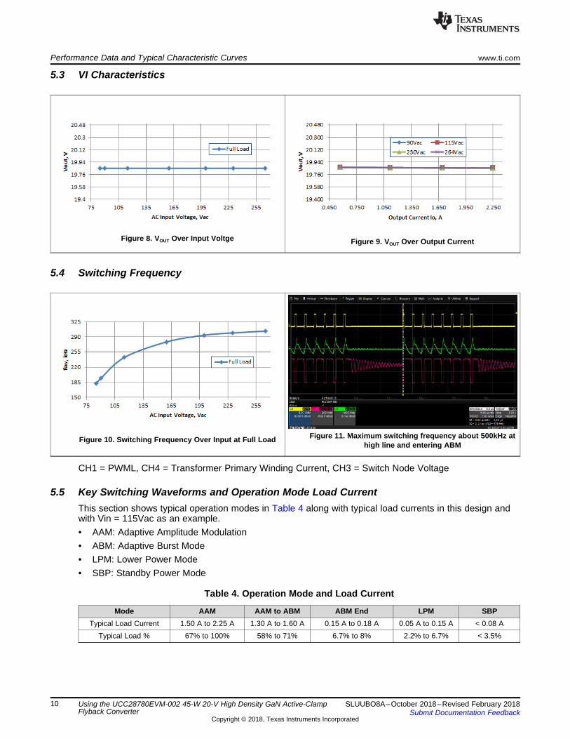
5.3 VI Characteristics
Figure 8. VOUT Over Input Voltge Figure 9. VOUT Over Output Current
5.4 Switching Frequency
Figure 10. Switching Frequency Over Input at Full Load Figure 11. Maximum switching frequency about 500kHz athigh line and entering ABM
CH1 = PWML, CH4 = Transformer Primary Winding Current, CH3 = Switch Node Voltage
5.5 Key Switching Waveforms and Operation Mode Load CurrentThis section shows typical operation modes in Table 4 along with typical load currents in this design andwith Vin = 115Vac as an example.• AAM: Adaptive Amplitude Modulation• ABM: Adaptive Burst Mode• LPM: Lower Power Mode• SBP: Standby Power Mode
Table 4. Operation Mode and Load Current
Mode AAM AAM to ABM ABM End LPM SBPTypical Load Current 1.50 A to 2.25 A 1.30 A to 1.60 A 0.15 A to 0.18 A 0.05 A to 0.15 A < 0.08 A
Typical Load % 67% to 100% 58% to 71% 6.7% to 8% 2.2% to 6.7% < 3.5%

www.ti.com Performance Data and Typical Characteristic Curves
11SLUUBO8A–October 2018–Revised February 2018Submit Documentation Feedback
Copyright © 2018, Texas Instruments Incorporated
Using the UCC28780EVM-002 45-W 20-V High Density GaN Active-ClampFlyback Converter
Figure 12. AAM Mode at Heavy Loads (CH1 = PWML, CH4= Transformer Primary Winding Current, CH2 = Switch
Node Voltage, CH3 = PWMH)
Figure 13. ABM Mode at Medium Loads (CH1 = PWML,CH4 = Transformer Primary Winding Current, CH2 =
Switch Node Voltage)
Figure 14. ABM Mode and SR (CH1 = PWML, CH4 =Transformer Primary Winding Current, CH2 = Switch Node
Voltage, CH3 = SR Vgs)
Figure 15. Recovery after OPP with 3 Stages of PeakCurrent (CH1 = PWML, CH4 = Transformer Primary
Winding Current, CH2 = Switch Node Voltage)
Figure 16. LPM Mode Operation (when a burst packetcontains 2 pulses and the interval between 2 packets isaround 40µs, and peak current starts to reduce. CH3 =PWML, CH4 = Transformer primary winding current.)
Figure 17. SBP Mode Operation(when a burst packet contains 2 pulses and the interval
between 2 packets is > 40 µs. CH3 = PWML, CH4 =Transformer primary winding current.)

Performance Data and Typical Characteristic Curves www.ti.com
12 SLUUBO8A–October 2018–Revised February 2018Submit Documentation Feedback
Copyright © 2018, Texas Instruments Incorporated
Using the UCC28780EVM-002 45-W 20-V High Density GaN Active-ClampFlyback Converter
5.6 Start UpCH1 = PWML, CH2 = Switch Node Voltage, CH3 = Output Voltage, CH4 = Transformer Primary Current.
Figure 18. 115 VAC and Full Load Startup Figure 19. 230 VAC and Full Load Startup
5.7 Line Transient ResponseCH1 = Vout, CH2 = Line voltage.
Figure 20. Output Voltage Response to Line Transient withFull Load.
Figure 21. Output Voltage Response to Line Transient withNo Load.

www.ti.com Performance Data and Typical Characteristic Curves
13SLUUBO8A–October 2018–Revised February 2018Submit Documentation Feedback
Copyright © 2018, Texas Instruments Incorporated
Using the UCC28780EVM-002 45-W 20-V High Density GaN Active-ClampFlyback Converter
5.8 Output Ripple VoltageCH3 = Output Voltage Ripple
Figure 22. Ripple Voltage = 40.0mV, VIN = 115 VRMS, IOUT =2.25 A
Figure 23. Ripple Voltage = 38.6mV, VIN = 230 VRMS, IOUT =2.25 A
Figure 24. Ripple Voltage < 80 mV, VIN = 115VRMS, IOUT =1.125 A
Figure 25. Ripple Voltage < 80mV, VIN = 230VRMS, IOUT =1.125 A
Figure 26. Ripple Voltage = 24.3 mV, VIN = 115VRMS, IOUT = 0A
Figure 27. Ripple Voltage = 24.3mV, VIN = 230VRMS, IOUT = 0A

Performance Data and Typical Characteristic Curves www.ti.com
14 SLUUBO8A–October 2018–Revised February 2018Submit Documentation Feedback
Copyright © 2018, Texas Instruments Incorporated
Using the UCC28780EVM-002 45-W 20-V High Density GaN Active-ClampFlyback Converter
5.9 Over Power ProtectionFigure 28 shows the converter Over Power Protection (OPP) with respect to input voltage. Figure 29shows the converter auto-retry to resume operation after OPP.
Figure 28. OPP with Respect to Input Voltage
Figure 29. OPP Auto Retry (CH1 = PWML, CH2 = SwitchNode Voltage, CH3 = Transformer Primary Current)

www.ti.com Performance Data and Typical Characteristic Curves
15SLUUBO8A–October 2018–Revised February 2018Submit Documentation Feedback
Copyright © 2018, Texas Instruments Incorporated
Using the UCC28780EVM-002 45-W 20-V High Density GaN Active-ClampFlyback Converter
5.10 Load Transient Response
Figure 30 and Figure 31 show output voltage Vout deviation < 5% for 0 and 2.25A load step change.
CH3 = Vout, CH4 = Load Current.
Figure 30. Vout Load Transient Response at VIN = 115 VRMS Figure 31. Vout Load Transient Response at VIN = 230 VRMS
Figure 32 and Figure 33 show the switching node voltage response for 0 and 2.25A load step change.
CH2 = PWML, CH3 = Switch Node Voltage, CH4 = Load Current.
Figure 32. Load Step-Up (0A to 2.25A) SwitchingResponse
Figure 33. Load Step-Down (2.25A to 0A) SwitchingResponse

Performance Data and Typical Characteristic Curves www.ti.com
16 SLUUBO8A–October 2018–Revised February 2018Submit Documentation Feedback
Copyright © 2018, Texas Instruments Incorporated
Using the UCC28780EVM-002 45-W 20-V High Density GaN Active-ClampFlyback Converter
5.11 Conducted EMI Output Not Grounded to LISN ground
Figure 34. VIN = 115 VRMS, Load = 9.3 Ω Figure 35. VIN = 230 VRMS, Load = 9.3 Ω
NOTE: Please note this was evaluated on an EMI station for pre-qualification purpose only. It isrecommended that all final designs be verified by an agency qualified EMI test house.

www.ti.com Performance Data and Typical Characteristic Curves
17SLUUBO8A–October 2018–Revised February 2018Submit Documentation Feedback
Copyright © 2018, Texas Instruments Incorporated
Using the UCC28780EVM-002 45-W 20-V High Density GaN Active-ClampFlyback Converter
5.12 Thermal Images at Full Load (2.25 A)
Figure 36. VIN = 90 VAC, Top Side (Transformer: 60 °C) Figure 37. VIN = 90 VAC, Bottom Side (Q1: 64 °C; U7: 63 °C;DB1: 64 °C)
Figure 38. VIN = 115 VAC, Top Side (Transformer: 59 °C) Figure 39. VIN = 115 VAC, Bottom Side (Q1: 59 °C; U7: 56 °C)
Figure 40. VIN = 230 VAC, Top Side (Transformer: 66 °C) Figure 41. VIN = 230 VAC, Bottom Side (Q1: 76 °C)

Performance Data and Typical Characteristic Curves www.ti.com
18 SLUUBO8A–October 2018–Revised February 2018Submit Documentation Feedback
Copyright © 2018, Texas Instruments Incorporated
Using the UCC28780EVM-002 45-W 20-V High Density GaN Active-ClampFlyback Converter
Figure 42. VIN = 265 VAC, Top Side (Transformer: 69 °C) Figure 43. VIN = 265 VAC, Bottom Side (Q1: 79 °C)

www.ti.com Transformer Details
19SLUUBO8A–October 2018–Revised February 2018Submit Documentation Feedback
Copyright © 2018, Texas Instruments Incorporated
Using the UCC28780EVM-002 45-W 20-V High Density GaN Active-ClampFlyback Converter
6 Transformer DetailsPrecision Inc transformer part number 019-8916-00R is used on this design and wound on a low profileRM8/ILP core set (11.6 mm height).
Figure 44. Transformer Schematic Diagram
Sh1 and Sh2 are the terminals for EMI shields. Their optimal connections are to be determined and theircurrent connections are to pin P1.
Table 5. Transformer Specifications at 25°C
PARAMETER VALUE PINS/LEADS TEST CONDITIONSInductance (µH) 104 to 127 P1 – P2 Open all other pins
Leakage Inductance (µH) 2.5 Max. P1 – P2 Tie S1 - S2, 0.1 V, 200 kHzD.C. resistance (Ω) 0.147 Max. P1 – P2D.C. resistance (Ω) 0.014 Max. S1 – S2D.C. resistance (Ω) 0.16 Max. Pa1 – Pa2D.C. resistance (Ω) 0.168 Max. Sa1 – Sa2
Dielectric (VAC) 1500 P1 – S1 1 mA, 60 Hz, 1 sDielectric (VAC) 500 P1, S1 to Core 1 mA, 60 Hz, 1 s
Turns ratio 1:0.19:0.14:0.1 (P1-P2):(S1-S2):(Pa1-Pa2):(Sa1-Sa2)

EVM Assembly and Layout www.ti.com
20 SLUUBO8A–October 2018–Revised February 2018Submit Documentation Feedback
Copyright © 2018, Texas Instruments Incorporated
Using the UCC28780EVM-002 45-W 20-V High Density GaN Active-ClampFlyback Converter
7 EVM Assembly and Layout
Figure 45. EVM Assembly (Top View)
Figure 46. EVM Assembly (Bottom View)

www.ti.com List of Materials
21SLUUBO8A–October 2018–Revised February 2018Submit Documentation Feedback
Copyright © 2018, Texas Instruments Incorporated
Using the UCC28780EVM-002 45-W 20-V High Density GaN Active-ClampFlyback Converter
8 List of MaterialsUCC28780EVM-002 (secondary resonance approach as default) list of materials for the schematicdiagrams shown in Figure 3 and in Figure 4. At bottom of the table, a component change list shows howto modify the design to obtain the primary resonance.
Table 6. UCC28780EVM-002 List of Materials
Quantity Designator Description PartNumber Manufacturer2 C1, C2 Capacitor, aluminum, 39 µF, 400 V, ±20%, AEC-
Q200 Grade 2, THEKXJ401ELL390MU20S Chemi-Con
4 C3, C4, C5,C17
Capacitor, ceramic, 0.1 µF, 450 V, ±10%, X7T,1206_190
C3216X7T2W104K160AA TDK
2 C6, C24 Capacitor, ceramic, 0.22 µF, 250 V, ±10%, X7T,AEC-Q200 Grade 1, 1206
CGA5L3X7T2E224K160AE
TDK
1 C7 Capacitor, ceramic, 24 pF, 50 V, ±5%, C0G/NP0,0402
GRM1555C1H240JA01D MuRata
2 C8, C9 Capacitor, ceramic, 33 µF, 25 V, 20%, JB, 1206 C3216JB1E336M160AC MuRata1 C10 Do Not Populate1 C11 Capacitor, ceramic, 180 pF, 50 V, 1%, C0G/NP0,
040204025A181FAT2A AVX
1 C12 CAP, Film, 0.068 µF, X2 275 VAC, +/- 10%, TH 890324022017CS Wurth Elektronik1 C13 Capacitor, ceramic, 330 PF, 250 V, C0G/NP0,
0805GRM21A5C2E331JW01D MuRata
1 C14 Capacitor, ceramic, 33 pF, X1/Y2 250 VAC, ±5%,SL, D7xT5mm
DE21XKY330JN3AM02F TDK
2 C15, C25 Capacitor, ceramic, 22 µF, 35 V, ±20%, X5R, 0805 C2012X5R1V226M125AC TDK1 C16 Capacitor, AL Poly, 680 µF, 25V, ±20%, TH 687AVG025MGBJ Illinois Capacitor1 C18 Capacitor, ceramic, 2200 pF, 50 V, ±10%, X7R,
0402CGA2B2X7R1H222K050BA
TDK
1 C19 Capacitor, ceramic, 2.2 µF, 50 V, ±10%, X7R, 0805 C2012X7R1H225K125AC TDK1 20 Capacitor, ceramic, 22 pF, 50 V, ±5%, C0G/NP0,
0402GRM1555C1H220JA01D MuRata
1 C21 Capacitor, ceramic, 0.1 µF, 25 V, ±10%, X7R, 0402 GRM155R71E104KE14D MuRata1 C22 Capacitor, ceramic, 0.022 µF, 50V, ±5%, X7R,
0402CGA2B2X7R1H472K050BA
TDK
5 C30, C32, C34,C35, C36
Capacitor, ceramic, 0.047 µF, 50V, 10%, X7R,0402
GRM155R71H223KA12D MuRata
2 C23, C26 Capacitor, ceramic, 680 pF, X1 250 VAC/Y2 250VAC, +/- 10%, X7R, 2211
GA352QR7GF681KW01L MuRata
1 C27 Capacitor, ceramic, 3.3 pF, 50 V, ±8%, C0G/NP0,0603
06035A3R3CAT2A AVX
1 C28 Capacitor, ceramic, 10 nF, 50 V, ±5%, C0G/NP0,0603
CGA3E2C0G1H103J080AA
TDK
1 C29 Capacitor, ceramic, 1 µF, 50 V, ±10%, X7R, AEC-Q200 Grade 1, 0805
CGA4J3X7R1H105K125AB
TDK
2 C31, C33 Capacitor, ceramic, 0.01 µF, 50 V, ±10%, X7R,0402
GRM155R71H103KA88D MuRata
1 D1 Diode, superfast rectifier, 600 V, 1 A, 3.5x1.6mm CSFMT108-HF ComchipTechnology
1 D2 Diode, ultrafast, 100 V, 0.15 A, SOD-123 1N4148W-7-F Diodes Inc.1 D3 Diode, Zener, 22 V, 300 mW, SOD-523 BZT52C22T-7 Diodes Inc.1 D4 Diode, TVS, Uni, 18V, SOD-323 CDSOD323-T18 Bourns2 D5, D9 Diode, Zener, 6.2 V, 150 mW, SOD-523F CZRU52C6V2 Comchip
Technology2 D6, D10 Diode, Zener, 2 V, 150 mW, SOD-523F CZRU52C2 Comchip
Technology1 D7 Diode, Schottky, 40 V, 0.03 A, SOD-523 SDM03U40-7 Diodes Inc.

List of Materials www.ti.com
22 SLUUBO8A–October 2018–Revised February 2018Submit Documentation Feedback
Copyright © 2018, Texas Instruments Incorporated
Using the UCC28780EVM-002 45-W 20-V High Density GaN Active-ClampFlyback Converter
Table 6. UCC28780EVM-002 List of Materials (continued)Quantity Designator Description PartNumber Manufacturer
1 D8 Diode, Ultrafast, 600 V, 1 A, AEC-Q101, SMAF ES1JAF Fairchild Semi1 DB1 Diode, P-N-bridge, 1000 V, 4 A, Z4-D Z4DGP410L-HF Comchip
Technology1 F1 Fuse, 2.5 A, 250 VAC/VDC, TH RST 2.5-Bulk Bel-Fuse1 L1 Inductor, unshielded Drum Core, Ferrite, 22 µH,
1.7 A, 0.102 Ω, TH7447462220 Wurth Elektronik
1 L2 Coupled inductor, 0.014 Ω, TH 019-8917-00R PrecisionIncorporated
1 L3 Inductor, Unshielded Drum Core, Ferrite, 1 µH, 8A, 0.006 ohm, TH
7447462010 Wurth Elektronik
1 L4 Inductor, Multilayer, Ferrite, 0.68 µH, 0.19 A, 0.67ohm, 1206
LQH31MNR68K03L MuRata
1 Q1 MOSFET, N-Channel, 150 V, 87 A, PG-TDSON-8 BSC160N15NS5ATMA1 InfineonTechnologies
1 Q2 MOSFET, N-Channel, 600 V, 0.021 A, AEC-Q101,SOT-23
BSS126H6327XTSA2 InfineonTechnologies
1 Q3 MOSFET, P-CH, -50 V, -0.13 A, SOT-323 BSS84W-7-F Diodes Inc.2 Q4, Q5 MOSFET, N-CH, 60 V, 0.17 A, SOT-23 2N7002-7-F Diodes Inc.1 R1 Resistor, 1.00 k, 1%, 0.1 W, 0603 ERJ-3EKF1001V Panasonic1 R2 Resistor, 2.21 MΩ, 1%, 0.25 W, 1206 CRCW12062M21FKEA Vishay-Dale1 R3 Resistor, 0 Ω, 5%, 0.1 W, 0603 CRCW06030000Z0EA Vishay-Dale3 R4, R12, R23 Resistor, 10.0 Ω, 1%, 0.063 W, 0402 ERJ-2RKF10R0X Panasonic1 R5 Resistor, 33 Ω, 5%, 0.125 W, 0805 CRCW080533R0JNEA Vishay-Dale1 R6 Resistor, 49.9 Ω, 1%, 0.1 W, 0402 ERJ-2RKF49R9X Panasonic1 R7 Resistor, 196 kΩ, 1%, 0.063 W, 0402 CRCW0402196KFKED Vishay-Dale1 R8 Resistor, 536, 1%, 0.063 W, 0402 RC0402FR-07536RL Yageo1 R9 Resistor, 22.1kΩ, 1%, 0.063 W, 0402 CRCW040222K1FKED Vishay-Dale1 R10 Resistor, 249 kΩ, 1%, 0.063 W, 0402 CRCW0402249KFKED Vishay-Dale2 R11, R14 Resistor, 11.0 k, 1%, 0.063 W, 0402 CRCW040211K0FKED Vishay-Dale1 R13 Resistor, 34.0 k, 1%, 0.063 W, 0402 CRCW040234K0FKED Vishay-Dale1 R15 Resistor, 95.3 k, 1%, 0.063 W, 0402 RC0402FR-0795K3L Yageo1 R16 Resistor, 63.4 kΩ, 1%, 0.063 W, 0402 CRCW040263K4FKED Vishay-Dale1 R17 Resistor, 2.49, 1%, 0.1 W, 0603 RC0603FR-072R49L Yageo4 R18, R19, R20,
R21Resistor, 0.91 Ω, 1%, 0.125 W, 0805 RL0805FR-070R91L Yageo
1 R22 Resistor, 121 Ω, 1%, 0.063 W, 0402 CRCW0402121RFKED Vishay-Dale1 R24 Resistor, 21.5 kΩ, 1%, 0.063 W, 0402 CRCW040221K5FKED Vishay-Dale1 R25 Resistor, 820 Ω, 1%, 0.1 W, 0603 RC0603FR-07820RL Yageo America1 R26 Resistor, 150 kΩ, 1%, 0.1 W, 0603 RC0603FR-07150KL Yageo America1 R27 Resistor, 60.4 kΩ, 1%, 0.063 W, 0402 CRCW040260K4FKED Vishay-Dale1 R28 Resistor, 1.00 MΩ, 1%, 0.1 W, 0603 CRCW06031M00FKEA Vishay-Dale1 R29 Resistor, 36.5 kΩ, 1%, 0.125 W, 0805 CRCW080536K5FKEA Vishay-Dale2 R30, R33 Resistor, 10.0, 1%, 0.063 W, 0402 RC0402FR-0710RL Yageo1 R31 Resistor, 5.1, 5%, 0.063 W, 0402 RC0402JR-075R1L Yageo1 R32 Resistor, 100, 5%, 0.1 W, 0402 'ERJ-2GEJ101X Panasonic1 R34 Resistor, 4.99 kΩ, 1%, 0.063 W, 0402 RC0402FR-074K99L Yageo1 R35 Resistor, 49.9 kΩ, 1%, 0.063 W, 0402 RC0402FR-0749K9L Yageo2 R36, R37 Resistor, 100 kΩ, 5%, 0.1 W, 0402 ERJ-2GEJ104X Panasonic1 R38 Resistor, 750 kΩ, 1%, 0.1 W, 0402 CRCW0402750KFKED Vishay-Dale1 RT1 Thermistor NTC, 47 kΩ, 5%, 0603 NCP18WB473J03RB MuRata

www.ti.com Revision History
23SLUUBO8A–October 2018–Revised February 2018Submit Documentation Feedback
Copyright © 2018, Texas Instruments Incorporated
Revision History
Table 6. UCC28780EVM-002 List of Materials (continued)Quantity Designator Description PartNumber Manufacturer
1 T1 Transformer, 115 µH, TH 019-8916-00R PrecisionIncorporated
1 U1 Optocoupler, 3.75 kV, 80-160% CTR, SMT FODM8801AV Fairchild Semi1 U2 Adjustable Precision Shunt Regulator, SOT23-3 ATL431BQDBZR Texas Instruments1 U3 UCC24612-1DBV, DBV0005A (SOT-23-5) UCC24612-1DBVR Texas Instruments1 U4 High Speed, Digital Isolator, SOIC-8 ISO7710FD Texas Instruments1 U5 Active-Clamp Flyback Controller, RTE0016C (QFN-
16)UCC28780RTER Texas Instruments
1 U6 650V AllGaN Power IC with iDrive, PQFN-8 NV6117 Navitas Semi1 U7 650V AllGaN Power IC with iDrive, PQFN-8 NV6115 Navitas Semi
Revision HistoryNOTE: Page numbers for previous revisions may differ from page numbers in the current version.
Changes from Original (October 2017) to A Revision .................................................................................................... Page
• Changed the primary GaN MOSFETs from NV6250 to NV6115 + NV6117 ...................................................... 4• Changed the electrical performance and specifications.............................................................................. 4• Changed the Schematic Diagram with NV6115 + NV6117.......................................................................... 5• Changed test results of efficiency, switching frequency, and output V-I characteristics......................................... 9• Changed the output voltage ripple waveforms....................................................................................... 13• Changed the over power protection characteristics ................................................................................. 14• Changed the load transient response................................................................................................. 15• Changed the EMI test results .......................................................................................................... 16

STANDARD TERMS FOR EVALUATION MODULES1. Delivery: TI delivers TI evaluation boards, kits, or modules, including any accompanying demonstration software, components, and/or
documentation which may be provided together or separately (collectively, an “EVM” or “EVMs”) to the User (“User”) in accordancewith the terms set forth herein. User's acceptance of the EVM is expressly subject to the following terms.1.1 EVMs are intended solely for product or software developers for use in a research and development setting to facilitate feasibility
evaluation, experimentation, or scientific analysis of TI semiconductors products. EVMs have no direct function and are notfinished products. EVMs shall not be directly or indirectly assembled as a part or subassembly in any finished product. Forclarification, any software or software tools provided with the EVM (“Software”) shall not be subject to the terms and conditionsset forth herein but rather shall be subject to the applicable terms that accompany such Software
1.2 EVMs are not intended for consumer or household use. EVMs may not be sold, sublicensed, leased, rented, loaned, assigned,or otherwise distributed for commercial purposes by Users, in whole or in part, or used in any finished product or productionsystem.
2 Limited Warranty and Related Remedies/Disclaimers:2.1 These terms do not apply to Software. The warranty, if any, for Software is covered in the applicable Software License
Agreement.2.2 TI warrants that the TI EVM will conform to TI's published specifications for ninety (90) days after the date TI delivers such EVM
to User. Notwithstanding the foregoing, TI shall not be liable for a nonconforming EVM if (a) the nonconformity was caused byneglect, misuse or mistreatment by an entity other than TI, including improper installation or testing, or for any EVMs that havebeen altered or modified in any way by an entity other than TI, (b) the nonconformity resulted from User's design, specificationsor instructions for such EVMs or improper system design, or (c) User has not paid on time. Testing and other quality controltechniques are used to the extent TI deems necessary. TI does not test all parameters of each EVM.User's claims against TI under this Section 2 are void if User fails to notify TI of any apparent defects in the EVMs within ten (10)business days after delivery, or of any hidden defects with ten (10) business days after the defect has been detected.
2.3 TI's sole liability shall be at its option to repair or replace EVMs that fail to conform to the warranty set forth above, or creditUser's account for such EVM. TI's liability under this warranty shall be limited to EVMs that are returned during the warrantyperiod to the address designated by TI and that are determined by TI not to conform to such warranty. If TI elects to repair orreplace such EVM, TI shall have a reasonable time to repair such EVM or provide replacements. Repaired EVMs shall bewarranted for the remainder of the original warranty period. Replaced EVMs shall be warranted for a new full ninety (90) daywarranty period.
3 Regulatory Notices:3.1 United States
3.1.1 Notice applicable to EVMs not FCC-Approved:FCC NOTICE: This kit is designed to allow product developers to evaluate electronic components, circuitry, or softwareassociated with the kit to determine whether to incorporate such items in a finished product and software developers to writesoftware applications for use with the end product. This kit is not a finished product and when assembled may not be resold orotherwise marketed unless all required FCC equipment authorizations are first obtained. Operation is subject to the conditionthat this product not cause harmful interference to licensed radio stations and that this product accept harmful interference.Unless the assembled kit is designed to operate under part 15, part 18 or part 95 of this chapter, the operator of the kit mustoperate under the authority of an FCC license holder or must secure an experimental authorization under part 5 of this chapter.3.1.2 For EVMs annotated as FCC – FEDERAL COMMUNICATIONS COMMISSION Part 15 Compliant:
CAUTIONThis device complies with part 15 of the FCC Rules. Operation is subject to the following two conditions: (1) This device may notcause harmful interference, and (2) this device must accept any interference received, including interference that may causeundesired operation.Changes or modifications not expressly approved by the party responsible for compliance could void the user's authority tooperate the equipment.
FCC Interference Statement for Class A EVM devicesNOTE: This equipment has been tested and found to comply with the limits for a Class A digital device, pursuant to part 15 ofthe FCC Rules. These limits are designed to provide reasonable protection against harmful interference when the equipment isoperated in a commercial environment. This equipment generates, uses, and can radiate radio frequency energy and, if notinstalled and used in accordance with the instruction manual, may cause harmful interference to radio communications.Operation of this equipment in a residential area is likely to cause harmful interference in which case the user will be required tocorrect the interference at his own expense.

FCC Interference Statement for Class B EVM devicesNOTE: This equipment has been tested and found to comply with the limits for a Class B digital device, pursuant to part 15 ofthe FCC Rules. These limits are designed to provide reasonable protection against harmful interference in a residentialinstallation. This equipment generates, uses and can radiate radio frequency energy and, if not installed and used in accordancewith the instructions, may cause harmful interference to radio communications. However, there is no guarantee that interferencewill not occur in a particular installation. If this equipment does cause harmful interference to radio or television reception, whichcan be determined by turning the equipment off and on, the user is encouraged to try to correct the interference by one or moreof the following measures:
• Reorient or relocate the receiving antenna.• Increase the separation between the equipment and receiver.• Connect the equipment into an outlet on a circuit different from that to which the receiver is connected.• Consult the dealer or an experienced radio/TV technician for help.
3.2 Canada3.2.1 For EVMs issued with an Industry Canada Certificate of Conformance to RSS-210 or RSS-247
Concerning EVMs Including Radio Transmitters:This device complies with Industry Canada license-exempt RSSs. Operation is subject to the following two conditions:(1) this device may not cause interference, and (2) this device must accept any interference, including interference that maycause undesired operation of the device.
Concernant les EVMs avec appareils radio:Le présent appareil est conforme aux CNR d'Industrie Canada applicables aux appareils radio exempts de licence. L'exploitationest autorisée aux deux conditions suivantes: (1) l'appareil ne doit pas produire de brouillage, et (2) l'utilisateur de l'appareil doitaccepter tout brouillage radioélectrique subi, même si le brouillage est susceptible d'en compromettre le fonctionnement.
Concerning EVMs Including Detachable Antennas:Under Industry Canada regulations, this radio transmitter may only operate using an antenna of a type and maximum (or lesser)gain approved for the transmitter by Industry Canada. To reduce potential radio interference to other users, the antenna typeand its gain should be so chosen that the equivalent isotropically radiated power (e.i.r.p.) is not more than that necessary forsuccessful communication. This radio transmitter has been approved by Industry Canada to operate with the antenna typeslisted in the user guide with the maximum permissible gain and required antenna impedance for each antenna type indicated.Antenna types not included in this list, having a gain greater than the maximum gain indicated for that type, are strictly prohibitedfor use with this device.
Concernant les EVMs avec antennes détachablesConformément à la réglementation d'Industrie Canada, le présent émetteur radio peut fonctionner avec une antenne d'un type etd'un gain maximal (ou inférieur) approuvé pour l'émetteur par Industrie Canada. Dans le but de réduire les risques de brouillageradioélectrique à l'intention des autres utilisateurs, il faut choisir le type d'antenne et son gain de sorte que la puissance isotroperayonnée équivalente (p.i.r.e.) ne dépasse pas l'intensité nécessaire à l'établissement d'une communication satisfaisante. Leprésent émetteur radio a été approuvé par Industrie Canada pour fonctionner avec les types d'antenne énumérés dans lemanuel d’usage et ayant un gain admissible maximal et l'impédance requise pour chaque type d'antenne. Les types d'antennenon inclus dans cette liste, ou dont le gain est supérieur au gain maximal indiqué, sont strictement interdits pour l'exploitation del'émetteur
3.3 Japan3.3.1 Notice for EVMs delivered in Japan: Please see http://www.tij.co.jp/lsds/ti_ja/general/eStore/notice_01.page 日本国内に
輸入される評価用キット、ボードについては、次のところをご覧ください。http://www.tij.co.jp/lsds/ti_ja/general/eStore/notice_01.page
3.3.2 Notice for Users of EVMs Considered “Radio Frequency Products” in Japan: EVMs entering Japan may not be certifiedby TI as conforming to Technical Regulations of Radio Law of Japan.
If User uses EVMs in Japan, not certified to Technical Regulations of Radio Law of Japan, User is required to follow theinstructions set forth by Radio Law of Japan, which includes, but is not limited to, the instructions below with respect to EVMs(which for the avoidance of doubt are stated strictly for convenience and should be verified by User):1. Use EVMs in a shielded room or any other test facility as defined in the notification #173 issued by Ministry of Internal
Affairs and Communications on March 28, 2006, based on Sub-section 1.1 of Article 6 of the Ministry’s Rule forEnforcement of Radio Law of Japan,
2. Use EVMs only after User obtains the license of Test Radio Station as provided in Radio Law of Japan with respect toEVMs, or
3. Use of EVMs only after User obtains the Technical Regulations Conformity Certification as provided in Radio Law of Japanwith respect to EVMs. Also, do not transfer EVMs, unless User gives the same notice above to the transferee. Please notethat if User does not follow the instructions above, User will be subject to penalties of Radio Law of Japan.

【無線電波を送信する製品の開発キットをお使いになる際の注意事項】 開発キットの中には技術基準適合証明を受けていないものがあります。 技術適合証明を受けていないもののご使用に際しては、電波法遵守のため、以下のいずれかの措置を取っていただく必要がありますのでご注意ください。1. 電波法施行規則第6条第1項第1号に基づく平成18年3月28日総務省告示第173号で定められた電波暗室等の試験設備でご使用
いただく。2. 実験局の免許を取得後ご使用いただく。3. 技術基準適合証明を取得後ご使用いただく。
なお、本製品は、上記の「ご使用にあたっての注意」を譲渡先、移転先に通知しない限り、譲渡、移転できないものとします。上記を遵守頂けない場合は、電波法の罰則が適用される可能性があることをご留意ください。 日本テキサス・イ
ンスツルメンツ株式会社東京都新宿区西新宿6丁目24番1号西新宿三井ビル
3.3.3 Notice for EVMs for Power Line Communication: Please see http://www.tij.co.jp/lsds/ti_ja/general/eStore/notice_02.page電力線搬送波通信についての開発キットをお使いになる際の注意事項については、次のところをご覧ください。http://www.tij.co.jp/lsds/ti_ja/general/eStore/notice_02.page
3.4 European Union3.4.1 For EVMs subject to EU Directive 2014/30/EU (Electromagnetic Compatibility Directive):
This is a class A product intended for use in environments other than domestic environments that are connected to alow-voltage power-supply network that supplies buildings used for domestic purposes. In a domestic environment thisproduct may cause radio interference in which case the user may be required to take adequate measures.
4 EVM Use Restrictions and Warnings:4.1 EVMS ARE NOT FOR USE IN FUNCTIONAL SAFETY AND/OR SAFETY CRITICAL EVALUATIONS, INCLUDING BUT NOT
LIMITED TO EVALUATIONS OF LIFE SUPPORT APPLICATIONS.4.2 User must read and apply the user guide and other available documentation provided by TI regarding the EVM prior to handling
or using the EVM, including without limitation any warning or restriction notices. The notices contain important safety informationrelated to, for example, temperatures and voltages.
4.3 Safety-Related Warnings and Restrictions:4.3.1 User shall operate the EVM within TI’s recommended specifications and environmental considerations stated in the user
guide, other available documentation provided by TI, and any other applicable requirements and employ reasonable andcustomary safeguards. Exceeding the specified performance ratings and specifications (including but not limited to inputand output voltage, current, power, and environmental ranges) for the EVM may cause personal injury or death, orproperty damage. If there are questions concerning performance ratings and specifications, User should contact a TIfield representative prior to connecting interface electronics including input power and intended loads. Any loads appliedoutside of the specified output range may also result in unintended and/or inaccurate operation and/or possiblepermanent damage to the EVM and/or interface electronics. Please consult the EVM user guide prior to connecting anyload to the EVM output. If there is uncertainty as to the load specification, please contact a TI field representative.During normal operation, even with the inputs and outputs kept within the specified allowable ranges, some circuitcomponents may have elevated case temperatures. These components include but are not limited to linear regulators,switching transistors, pass transistors, current sense resistors, and heat sinks, which can be identified using theinformation in the associated documentation. When working with the EVM, please be aware that the EVM may becomevery warm.
4.3.2 EVMs are intended solely for use by technically qualified, professional electronics experts who are familiar with thedangers and application risks associated with handling electrical mechanical components, systems, and subsystems.User assumes all responsibility and liability for proper and safe handling and use of the EVM by User or its employees,affiliates, contractors or designees. User assumes all responsibility and liability to ensure that any interfaces (electronicand/or mechanical) between the EVM and any human body are designed with suitable isolation and means to safelylimit accessible leakage currents to minimize the risk of electrical shock hazard. User assumes all responsibility andliability for any improper or unsafe handling or use of the EVM by User or its employees, affiliates, contractors ordesignees.
4.4 User assumes all responsibility and liability to determine whether the EVM is subject to any applicable international, federal,state, or local laws and regulations related to User’s handling and use of the EVM and, if applicable, User assumes allresponsibility and liability for compliance in all respects with such laws and regulations. User assumes all responsibility andliability for proper disposal and recycling of the EVM consistent with all applicable international, federal, state, and localrequirements.
5. Accuracy of Information: To the extent TI provides information on the availability and function of EVMs, TI attempts to be as accurateas possible. However, TI does not warrant the accuracy of EVM descriptions, EVM availability or other information on its websites asaccurate, complete, reliable, current, or error-free.

6. Disclaimers:6.1 EXCEPT AS SET FORTH ABOVE, EVMS AND ANY MATERIALS PROVIDED WITH THE EVM (INCLUDING, BUT NOT
LIMITED TO, REFERENCE DESIGNS AND THE DESIGN OF THE EVM ITSELF) ARE PROVIDED "AS IS" AND "WITH ALLFAULTS." TI DISCLAIMS ALL OTHER WARRANTIES, EXPRESS OR IMPLIED, REGARDING SUCH ITEMS, INCLUDING BUTNOT LIMITED TO ANY EPIDEMIC FAILURE WARRANTY OR IMPLIED WARRANTIES OF MERCHANTABILITY OR FITNESSFOR A PARTICULAR PURPOSE OR NON-INFRINGEMENT OF ANY THIRD PARTY PATENTS, COPYRIGHTS, TRADESECRETS OR OTHER INTELLECTUAL PROPERTY RIGHTS.
6.2 EXCEPT FOR THE LIMITED RIGHT TO USE THE EVM SET FORTH HEREIN, NOTHING IN THESE TERMS SHALL BECONSTRUED AS GRANTING OR CONFERRING ANY RIGHTS BY LICENSE, PATENT, OR ANY OTHER INDUSTRIAL ORINTELLECTUAL PROPERTY RIGHT OF TI, ITS SUPPLIERS/LICENSORS OR ANY OTHER THIRD PARTY, TO USE THEEVM IN ANY FINISHED END-USER OR READY-TO-USE FINAL PRODUCT, OR FOR ANY INVENTION, DISCOVERY ORIMPROVEMENT, REGARDLESS OF WHEN MADE, CONCEIVED OR ACQUIRED.
7. USER'S INDEMNITY OBLIGATIONS AND REPRESENTATIONS. USER WILL DEFEND, INDEMNIFY AND HOLD TI, ITSLICENSORS AND THEIR REPRESENTATIVES HARMLESS FROM AND AGAINST ANY AND ALL CLAIMS, DAMAGES, LOSSES,EXPENSES, COSTS AND LIABILITIES (COLLECTIVELY, "CLAIMS") ARISING OUT OF OR IN CONNECTION WITH ANYHANDLING OR USE OF THE EVM THAT IS NOT IN ACCORDANCE WITH THESE TERMS. THIS OBLIGATION SHALL APPLYWHETHER CLAIMS ARISE UNDER STATUTE, REGULATION, OR THE LAW OF TORT, CONTRACT OR ANY OTHER LEGALTHEORY, AND EVEN IF THE EVM FAILS TO PERFORM AS DESCRIBED OR EXPECTED.
8. Limitations on Damages and Liability:8.1 General Limitations. IN NO EVENT SHALL TI BE LIABLE FOR ANY SPECIAL, COLLATERAL, INDIRECT, PUNITIVE,
INCIDENTAL, CONSEQUENTIAL, OR EXEMPLARY DAMAGES IN CONNECTION WITH OR ARISING OUT OF THESETERMS OR THE USE OF THE EVMS , REGARDLESS OF WHETHER TI HAS BEEN ADVISED OF THE POSSIBILITY OFSUCH DAMAGES. EXCLUDED DAMAGES INCLUDE, BUT ARE NOT LIMITED TO, COST OF REMOVAL ORREINSTALLATION, ANCILLARY COSTS TO THE PROCUREMENT OF SUBSTITUTE GOODS OR SERVICES, RETESTING,OUTSIDE COMPUTER TIME, LABOR COSTS, LOSS OF GOODWILL, LOSS OF PROFITS, LOSS OF SAVINGS, LOSS OFUSE, LOSS OF DATA, OR BUSINESS INTERRUPTION. NO CLAIM, SUIT OR ACTION SHALL BE BROUGHT AGAINST TIMORE THAN TWELVE (12) MONTHS AFTER THE EVENT THAT GAVE RISE TO THE CAUSE OF ACTION HASOCCURRED.
8.2 Specific Limitations. IN NO EVENT SHALL TI'S AGGREGATE LIABILITY FROM ANY USE OF AN EVM PROVIDEDHEREUNDER, INCLUDING FROM ANY WARRANTY, INDEMITY OR OTHER OBLIGATION ARISING OUT OF OR INCONNECTION WITH THESE TERMS, , EXCEED THE TOTAL AMOUNT PAID TO TI BY USER FOR THE PARTICULAREVM(S) AT ISSUE DURING THE PRIOR TWELVE (12) MONTHS WITH RESPECT TO WHICH LOSSES OR DAMAGES ARECLAIMED. THE EXISTENCE OF MORE THAN ONE CLAIM SHALL NOT ENLARGE OR EXTEND THIS LIMIT.
9. Return Policy. Except as otherwise provided, TI does not offer any refunds, returns, or exchanges. Furthermore, no return of EVM(s)will be accepted if the package has been opened and no return of the EVM(s) will be accepted if they are damaged or otherwise not ina resalable condition. If User feels it has been incorrectly charged for the EVM(s) it ordered or that delivery violates the applicableorder, User should contact TI. All refunds will be made in full within thirty (30) working days from the return of the components(s),excluding any postage or packaging costs.
10. Governing Law: These terms and conditions shall be governed by and interpreted in accordance with the laws of the State of Texas,without reference to conflict-of-laws principles. User agrees that non-exclusive jurisdiction for any dispute arising out of or relating tothese terms and conditions lies within courts located in the State of Texas and consents to venue in Dallas County, Texas.Notwithstanding the foregoing, any judgment may be enforced in any United States or foreign court, and TI may seek injunctive reliefin any United States or foreign court.
Mailing Address: Texas Instruments, Post Office Box 655303, Dallas, Texas 75265Copyright © 2018, Texas Instruments Incorporated

IMPORTANT NOTICE FOR TI DESIGN INFORMATION AND RESOURCES
Texas Instruments Incorporated (‘TI”) technical, application or other design advice, services or information, including, but not limited to,reference designs and materials relating to evaluation modules, (collectively, “TI Resources”) are intended to assist designers who aredeveloping applications that incorporate TI products; by downloading, accessing or using any particular TI Resource in any way, you(individually or, if you are acting on behalf of a company, your company) agree to use it solely for this purpose and subject to the terms ofthis Notice.TI’s provision of TI Resources does not expand or otherwise alter TI’s applicable published warranties or warranty disclaimers for TIproducts, and no additional obligations or liabilities arise from TI providing such TI Resources. TI reserves the right to make corrections,enhancements, improvements and other changes to its TI Resources.You understand and agree that you remain responsible for using your independent analysis, evaluation and judgment in designing yourapplications and that you have full and exclusive responsibility to assure the safety of your applications and compliance of your applications(and of all TI products used in or for your applications) with all applicable regulations, laws and other applicable requirements. Yourepresent that, with respect to your applications, you have all the necessary expertise to create and implement safeguards that (1)anticipate dangerous consequences of failures, (2) monitor failures and their consequences, and (3) lessen the likelihood of failures thatmight cause harm and take appropriate actions. You agree that prior to using or distributing any applications that include TI products, youwill thoroughly test such applications and the functionality of such TI products as used in such applications. TI has not conducted anytesting other than that specifically described in the published documentation for a particular TI Resource.You are authorized to use, copy and modify any individual TI Resource only in connection with the development of applications that includethe TI product(s) identified in such TI Resource. NO OTHER LICENSE, EXPRESS OR IMPLIED, BY ESTOPPEL OR OTHERWISE TOANY OTHER TI INTELLECTUAL PROPERTY RIGHT, AND NO LICENSE TO ANY TECHNOLOGY OR INTELLECTUAL PROPERTYRIGHT OF TI OR ANY THIRD PARTY IS GRANTED HEREIN, including but not limited to any patent right, copyright, mask work right, orother intellectual property right relating to any combination, machine, or process in which TI products or services are used. Informationregarding or referencing third-party products or services does not constitute a license to use such products or services, or a warranty orendorsement thereof. Use of TI Resources may require a license from a third party under the patents or other intellectual property of thethird party, or a license from TI under the patents or other intellectual property of TI.TI RESOURCES ARE PROVIDED “AS IS” AND WITH ALL FAULTS. TI DISCLAIMS ALL OTHER WARRANTIES ORREPRESENTATIONS, EXPRESS OR IMPLIED, REGARDING TI RESOURCES OR USE THEREOF, INCLUDING BUT NOT LIMITED TOACCURACY OR COMPLETENESS, TITLE, ANY EPIDEMIC FAILURE WARRANTY AND ANY IMPLIED WARRANTIES OFMERCHANTABILITY, FITNESS FOR A PARTICULAR PURPOSE, AND NON-INFRINGEMENT OF ANY THIRD PARTY INTELLECTUALPROPERTY RIGHTS.TI SHALL NOT BE LIABLE FOR AND SHALL NOT DEFEND OR INDEMNIFY YOU AGAINST ANY CLAIM, INCLUDING BUT NOTLIMITED TO ANY INFRINGEMENT CLAIM THAT RELATES TO OR IS BASED ON ANY COMBINATION OF PRODUCTS EVEN IFDESCRIBED IN TI RESOURCES OR OTHERWISE. IN NO EVENT SHALL TI BE LIABLE FOR ANY ACTUAL, DIRECT, SPECIAL,COLLATERAL, INDIRECT, PUNITIVE, INCIDENTAL, CONSEQUENTIAL OR EXEMPLARY DAMAGES IN CONNECTION WITH ORARISING OUT OF TI RESOURCES OR USE THEREOF, AND REGARDLESS OF WHETHER TI HAS BEEN ADVISED OF THEPOSSIBILITY OF SUCH DAMAGES.You agree to fully indemnify TI and its representatives against any damages, costs, losses, and/or liabilities arising out of your non-compliance with the terms and provisions of this Notice.This Notice applies to TI Resources. Additional terms apply to the use and purchase of certain types of materials, TI products and services.These include; without limitation, TI’s standard terms for semiconductor products http://www.ti.com/sc/docs/stdterms.htm), evaluationmodules, and samples (http://www.ti.com/sc/docs/sampterms.htm).
Mailing Address: Texas Instruments, Post Office Box 655303, Dallas, Texas 75265Copyright © 2018, Texas Instruments Incorporated