verification of singulated hbm2 stacks with a kgs test cell
TRANSCRIPT

Verification of Singulated HBM2 stacks with a KGS Test Cell
Dave ArmstrongToshiyuki Kiyokawa
Quay Nhin
Industry Need for High Performance HBM Memory– Performance benefits and application drivers– HBM process flow and critical test insertion point– Known good stack die probing key challenges
Probe card design challenges: probing on micro-bump at <60um pitch– Design rules for high speed– Space Transformation technology development
Direct on Micro-bump probing results– Overdrive versus probe force & probe diameter discussion – Ambient scrub mark pictures & result – High temperature scrub mark & test result
Actual ATE Signal output/input performance on HBM2 device– Simulation vs Actual Measurement result @ 2Gbps – 1ch drive vs 8ch simultaneous drive actual result– 1.6GHz/3.2Gbps simulation result
Proven benefits of this approach & Next Steps– Final product testing– High temperature and High frequency
Paper Discussion Outline
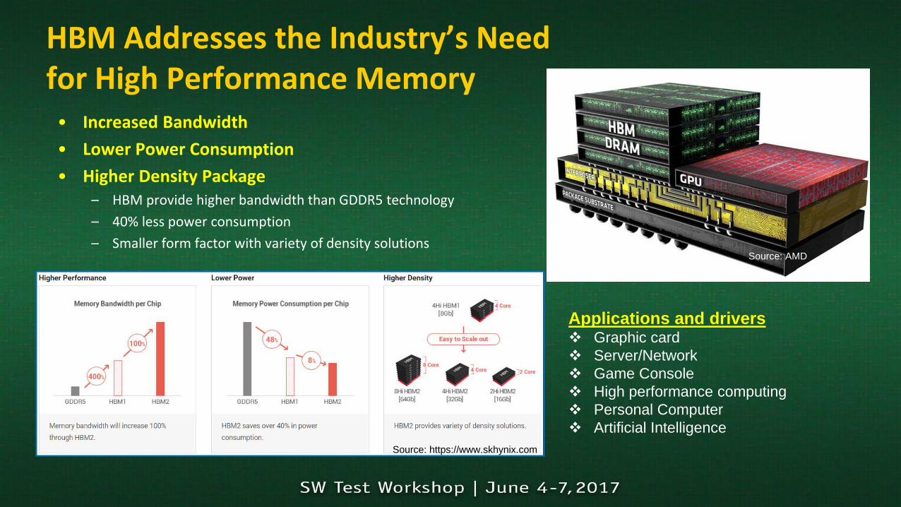
• Increased Bandwidth• Lower Power Consumption• Higher Density Package
– HBM provide higher bandwidth than GDDR5 technology– 40% less power consumption– Smaller form factor with variety of density solutions
HBM Addresses the Industry’s Needfor High Performance Memory
Applications and drivers Graphic card Server/Network Game Console High performance computing Personal Computer Artificial Intelligence
8Hi HBM2 [64Gb]Source: AMD
Source: https://www.skhynix.com

HBM Flow and KGSD Test Challenges
Post-stack WaferTest (PSWT) TestPad @Test Mode
Flip Dicing& Debonding
Shipment
wafer teststack & Mold
memory core
logic
Wafer/TSV process Thinning& Bump formation
Flip
wafer test
Wafer/TSV process Thinning& Bump formation
Flipdicing
Key Challengeso Handling of bare stack dieo Thermal movement o Contact stability at elevated temperatureo Micro-bump “coining” behavior at high temp
KGS Verification on µBump @Speed Test

• Contact all micro-bumps on HBM stacks to allow native mode functional and performance testing on all eight memory channels.
• Support at-speed testing > 2.4Gbps.
• Supports extreme temperature testing.
• Reliable contact to ~4,000 micro-bumps with a pitch of 55um.
Known-Good-Stack Testing Goals
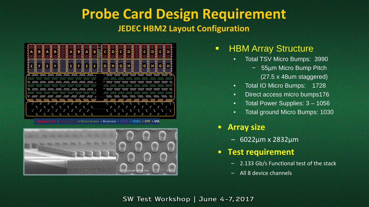
Probe Card Design RequirementJEDEC HBM2 Layout Configuration
HBM Array Structure• Total TSV Micro Bumps: 3990
− 55µm Micro Bump Pitch(27.5 x 48um staggered)
• Total IO Micro Bumps: 1728• Direct access micro bumps176• Total Power Supplies: 3 – 1056 • Total ground Micro Bumps: 1030
• Array size– 6022µm x 2832µm
• Test requirement– 2.133 Gb/s Functional test of the stack– All 8 device channels
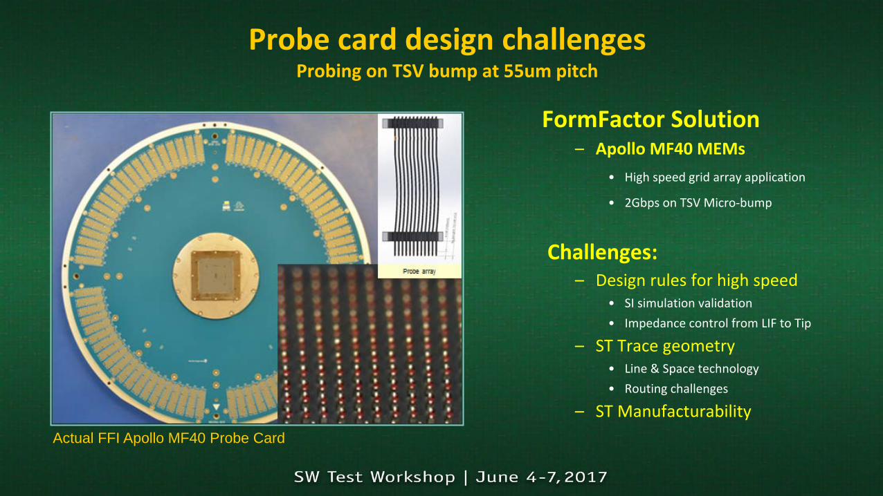
FormFactor Solution – Apollo MF40 MEMs
• High speed grid array application
• 2Gbps on TSV Micro-bump
Challenges:– Design rules for high speed
• SI simulation validation• Impedance control from LIF to Tip
– ST Trace geometry • Line & Space technology• Routing challenges
– ST Manufacturability
Probe card design challenges Probing on TSV bump at 55um pitch
Actual FFI Apollo MF40 Probe Card

Space Transformation Design Challenges
Small die size, high bump counts• ~4000 traces in ~6x3mm• FFI proprietary ST MLO fan-out
design enabler– Pushing the MLO technology limit– Co-develop additional capability for high
speed requirement– Line/space and layer count
• Impedance control optimization– Minimize voltage reflection & cross talk
8
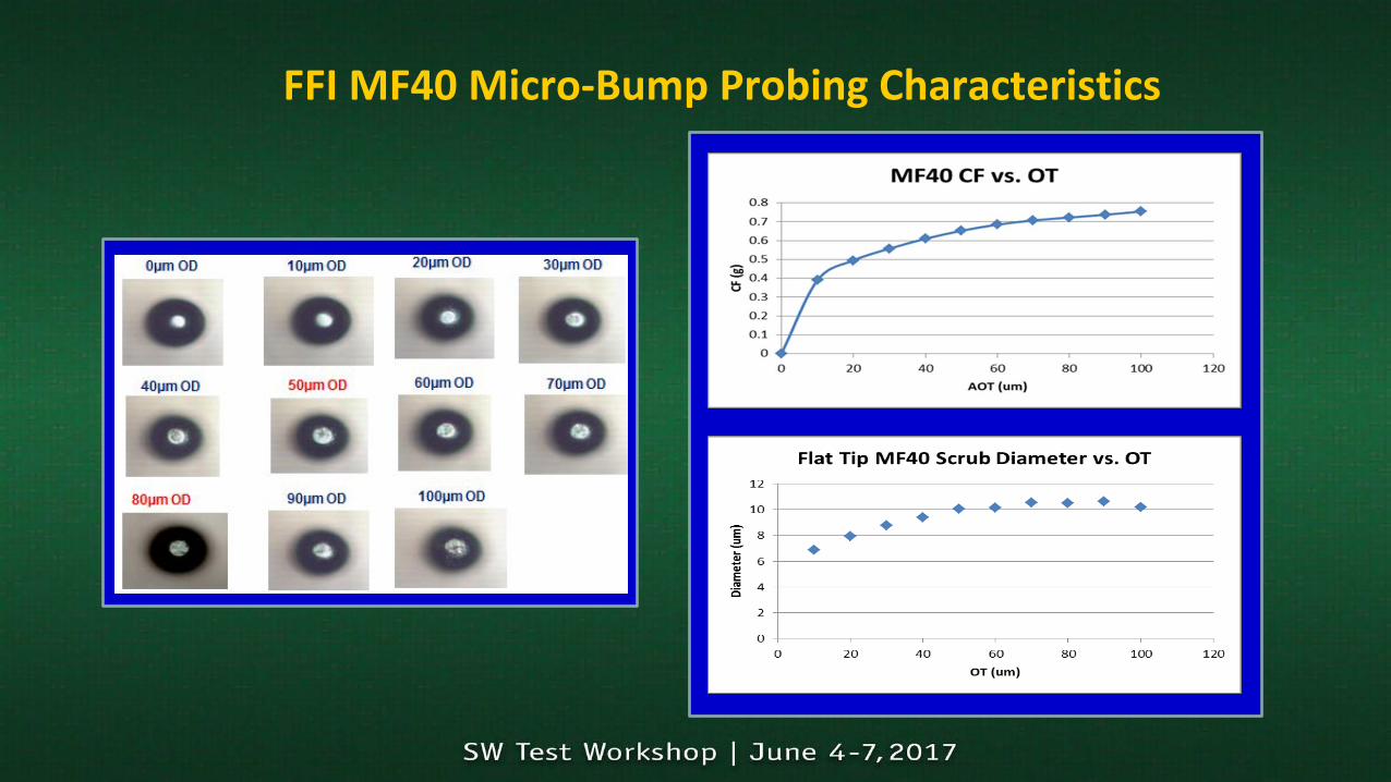
FFI MF40 Micro-Bump Probing Characteristics

• We succeeded in contacting all I/O pins• Ambient scrub mark pictures & result
– Contact Time:6sec, Contact : 1 time vs 2 times– Contact Time:600sec, Contact : 1 time vs 2 timesThe scrub becomes deeper as the number of contacts increases The scrub becomes deeper as the test time becomes longer
HBM2 Die Micro-bump Probing Results - Ambient
Condition T.T:6sec1 time
T.T:6sec2 times
Scrub depth[um] 0.87 1.72
Scrub diameter[um] 10.86 10.86
Condition T.T:600sec1 time
T.T:600sec2 times
Scrub depth[um] 2.61 2.99
Scrub diameter[um] 14.81 15.04
uBump Diameter : 25umOver Drive : 60umTemperature : Ambient

• We succeeded in contacting all I/O pins• High temperature scrub mark & test result
– Contact Time:6sec, Contact : 1 time vs 2 times– Contact Time:600sec, Contact : 1 time vs 2 timesThe scrub becomes deeper as the temperature becomes higher
HBM2 Die Micro-bump Probing Results – High Temperature
uBump Diameter : 25umOver Drive : 60umTemperature : 105degC
Condition T.T:6sec1 time
T.T:6sec2 times
Scrub depth[um] 1.66 1.84
Scrub diameter[um] 14.34 16.07
Condition T.T:600sec1 time
T.T:600sec2 times
Scrub depth[um] 2.80 3.86
Scrub diameter[um] 17.06 18.71

• Simulation vs Actual Measurement result @ 2Gbps – The waveform is similar in simulation and actual measurement on HBM2 die– Strong eye-diagram performance correlation
Signal Output/Input Performance on HBM2 Die
Simulation Actual Measurement
• PRBS signal driver and T5503HS’s comparator were terminated with 50Ω.
Simulation schematic of HBM as driver at 1 victim
ProbeCardModel
T5503PinElect.Model
PRBSPRBS
PRBSPRBS
VictimPRBS
EyeDiagram

• 1ch drive vs 8ch simultaneous drive actual result @ 2Gbps– With data activity on just one memory channel the output data eye width is quite large.– With data activity on all eight memory channels the output data eye shrinks.
Signal Output/Input Performance on HBM2 Die
Shmoo(Dout) 1ch meas. / 1ch drive Shmoo(Dout) 1ch meas. / 8ch drives

• 1.6GHz/3.2Gbps simulation result– MF40 technology supports operating speed to 3.2Gb/s with additional design rules optimization– Strong simulation versus actual measurement result as validated through ATE at 2Gbps
Signal Output/Input at Higher Frequency
T5503HS’sdriver model
Probe Card’smeasured S-para
eye-pattern evaluating point
S-para was measured by Network Analyzer up to10GHz.
Including HBM2IBIS model
DUT 3.2Gbps Signal Performance

• Working together as a team Advantest together with FormFactor developed a production worthy tool for confirming Known-Good Memory Stacks with ~4,000 micro-bumps and < 60um bump pitch.
• The resulting design exceeded our design goals for probe force and CCC with a wide operational temperature range.
• The solution exceeded our high frequency goal demonstrating >3 Gbps performance.
• The solution contacts to all eight HBM channels simultaneously enabling native mode performance and functional testing of these complex devices.
Benefit Summary

AcknowledgementSK Hynix
– Kim Wangki– Seo JaeHyoung
FormFactor Inc– Quay Nhin– Hirofumi Nagata– Uyen Nguyen– Todd Swart
Advantest– Toshiyuki Kiyokawa– Dave Armstrong– Masayoshi Ichikawa– Tetsuo Shikata– Koji Sakai– Lee Kyungeul– Kim Sangdeuk
16Author