high bandwidth memory (hbm2) interface intel® fpga ip ... · high bandwidth memory (hbm2)...
TRANSCRIPT

High Bandwidth Memory (HBM2)Interface Intel® FPGA IP DesignExample User Guide
Updated for Intel® Quartus® Prime Design Suite: 20.1
IP Version: 19.4.0
SubscribeSend Feedback
UG-20195 | 2020.04.13Latest document on the web: PDF | HTML

Contents
1. About the High Bandwidth Memory (HBM2) Interface Intel® FPGA IP............................ 31.1. Release Information...............................................................................................3
2. High Bandwidth Memory (HBM2) Interface Intel FPGA IP Design Example QuickStart Guide................................................................................................................ 42.1. Creating an Intel Quartus Prime Project for Your HBM2 System....................................42.2. Configuring the High Bandwidth Memory (HBM2) Interface Intel FPGA IP...................... 72.3. IP Parameter Editor Pro Guidelines for High Bandwidth Memory (HBM2) Interface
Intel FPGA IP......................................................................................................82.4. Generating the Synthesizable High Bandwidth Memory (HBM2) Interface Intel
FPGA IP Design Example.................................................................................... 102.5. Generating the Synthesizable High Bandwidth Memory (HBM2) Interface Intel
FPGA IP for High Efficiency................................................................................. 122.6. Generating the High Bandwidth Memory (HBM2) Interface Intel FPGA IP Design
Example for Simulation......................................................................................152.7. Regenerating the High Bandwidth Memory (HBM2) Interface Intel FPGA IP Design
Example After Modification................................................................................. 18
3. High Bandwidth Memory (HBM2) Interface Intel FPGA IP Design ExampleDescription.............................................................................................................. 203.1. High Bandwidth Memory (HBM2) Interface Intel FPGA IP Synthesis Design Example..... 203.2. High Bandwidth Memory (HBM2) Interface Intel FPGA IP Simulation Design Example.... 233.3. High Bandwidth Memory (HBM2) Interface Intel FPGA IP Design Example Interface
tab..................................................................................................................24
4. High Bandwidth Memory (HBM2) Interface Intel FPGA IP Design Example UserGuide Archives.........................................................................................................25
5. Document Revision History for the High Bandwidth Memory (HBM2) InterfaceIntel FPGA IP Design Example User Guide............................................................... 26
Contents
High Bandwidth Memory (HBM2) Interface Intel® FPGA IP Design ExampleUser Guide
Send Feedback
2
1. About the High Bandwidth Memory (HBM2) InterfaceIntel® FPGA IP
1.1. Release Information
IP versions are the same as the Intel® Quartus® Prime Design Suite software versionsup to v19.1. From Intel Quartus Prime Design Suite software version 19.2 or later, IPcores have a new IP versioning scheme.
The IP versioning scheme (X.Y.Z) number changes from one software version toanother. A change in:
• X indicates a major revision of the IP. If you update your Intel Quartus Primesoftware, you must regenerate the IP.
• Y indicates the IP includes new features. Regenerate your IP to include these newfeatures.
• Z indicates the IP includes minor changes. Regenerate your IP to include thesechanges.
Table 1.
Item Description
IP Version 19.4.0
Intel Quartus Prime Version 20.1
Release Date 2020.04.13
UG-20195 | 2020.04.13
Send Feedback
Intel Corporation. All rights reserved. Agilex, Altera, Arria, Cyclone, Enpirion, Intel, the Intel logo, MAX, Nios,Quartus and Stratix words and logos are trademarks of Intel Corporation or its subsidiaries in the U.S. and/orother countries. Intel warrants performance of its FPGA and semiconductor products to current specifications inaccordance with Intel's standard warranty, but reserves the right to make changes to any products and servicesat any time without notice. Intel assumes no responsibility or liability arising out of the application or use of anyinformation, product, or service described herein except as expressly agreed to in writing by Intel. Intelcustomers are advised to obtain the latest version of device specifications before relying on any publishedinformation and before placing orders for products or services.*Other names and brands may be claimed as the property of others.
ISO9001:2015Registered

2. High Bandwidth Memory (HBM2) Interface Intel FPGAIP Design Example Quick Start Guide
An automated design example flow is available for the High Bandwidth Memory(HBM2) Interface Intel FPGA IP.
You can use the Example Designs tab and the Generate Example Designs buttonin the IP Parameter Editor Pro window to specify and generate synthesis andsimulation example design file sets with which you can validate your HBM2 IP.
The generated design example reflects the parameterization that you set in the IPParameter Editor Pro window. You can generate a design example to specificallymatch an Intel FPGA development kit for your evaluation. Or you can generate adesign example to match your own actual system requirements, as a starting point forcreating your own system.
Figure 1. General Design Example Flow
Intel Quartus PrimeProject Creation
High Bandwidth Memory (HBM2)Interface Intel FPGAIP Configuration
Design Example Generation
Compilation(Quartus Prime)
Compilation(Simulator)
Functional Simulation
Timing Analysis(Quartus Prime)
Hardware Testing
2.1. Creating an Intel Quartus Prime Project for Your HBM2 System
To create a new IP variation, you must have an open Intel Quartus Prime project witha valid device part.If you do not already have an appropriate Intel Quartus Primeproject, follow these steps to create an Intel Quartus Prime project targeting a devicethat supports High Bandwidth Memory (HBM2) Interface Intel FPGA IP.
1. Launch the Intel Quartus Prime software and select File ➤ New Project Wizard.Click Next.
2. Specify a directory name (<user project directory>), a name for the Intel QuartusPrime project (<user project name>), and a top-level design entity name (<usertop-level instance name>) that you want to create. Click Next.
UG-20195 | 2020.04.13
Send Feedback
Intel Corporation. All rights reserved. Agilex, Altera, Arria, Cyclone, Enpirion, Intel, the Intel logo, MAX, Nios,Quartus and Stratix words and logos are trademarks of Intel Corporation or its subsidiaries in the U.S. and/orother countries. Intel warrants performance of its FPGA and semiconductor products to current specifications inaccordance with Intel's standard warranty, but reserves the right to make changes to any products and servicesat any time without notice. Intel assumes no responsibility or liability arising out of the application or use of anyinformation, product, or service described herein except as expressly agreed to in writing by Intel. Intelcustomers are advised to obtain the latest version of device specifications before relying on any publishedinformation and before placing orders for products or services.*Other names and brands may be claimed as the property of others.
ISO9001:2015Registered
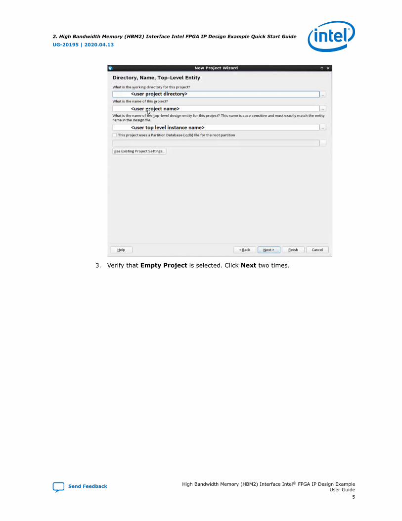
3. Verify that Empty Project is selected. Click Next two times.
2. High Bandwidth Memory (HBM2) Interface Intel FPGA IP Design Example Quick Start Guide
UG-20195 | 2020.04.13
Send Feedback High Bandwidth Memory (HBM2) Interface Intel® FPGA IP Design ExampleUser Guide
5

4. In the Device Family section of the dialog box, select Intel Stratix® 10 for theFamily and Stratix 10 MX for the Device. Alternatively, if you already know thespecific part number of the device that you want to use, type that device partnumber in the Name filter field.
Note: The generated HBM2 IP targets the specific Intel Stratix 10 MX device thatyou specify. Because different Intel Stratix 10 MX part numbers may identifydevices with differing numbers of HBM2 devices and differing HBM2 devicelocations, as well as differing stack count, height, and density properties, itis important that you specify the correct Intel Stratix 10 MX device partnumber before proceeding to the next step.
5. Select the appropriate device under Available Devices.
2. High Bandwidth Memory (HBM2) Interface Intel FPGA IP Design Example Quick Start Guide
UG-20195 | 2020.04.13
High Bandwidth Memory (HBM2) Interface Intel® FPGA IP Design ExampleUser Guide
Send Feedback
6

6. Click Finish. The system creates the (<user project directory>).qpf and(<user project directory>).qsf files within the (<user project directory>).
Figure 2. Generated Intel Quartus Prime Project and Settings File
<user project directory> - User actual Intel Prime Project directory
<user instance name> .qpf and <user instance name> .qsf – Generated Intel Quartus Prime project and setting fi les for user
<user project directory> - Your Intel Quartus Prime project directory
<user instance name>.qpf and <user instance name>.qsf - Generated Intel Quartus Prime project and settings files
2.2. Configuring the High Bandwidth Memory (HBM2) InterfaceIntel FPGA IP
The following steps illustrate the IP Catalog (standalone) configuration flow. ThePlatform Designer (standalone) flow is generally similar.
1. Verify that the IP Catalog window is visible. If the IP Catalog window is notvisible, select View ➤ Utility Windows ➤ IP Catalog.
2. In the IP Catalog window, select Installed IP ➤ Library ➤ Memory Interfacesand Controllers ➤ High Bandwidth Memory (HBM2) Interface Intel FPGAIP.
3. In the New IP Variant window, type a name (<user instance name>) for yourHBM2 IP in the File Name field. Click Create.
2. High Bandwidth Memory (HBM2) Interface Intel FPGA IP Design Example Quick Start Guide
UG-20195 | 2020.04.13
Send Feedback High Bandwidth Memory (HBM2) Interface Intel® FPGA IP Design ExampleUser Guide
7

4. In the IP Parameter Editor Pro window, configure the parameters on each tabto reflect your Intel FPGA development kit requirement or your actual HBM2interface and system requirement. For information on individual parameters, referto the Parameterizing the High Bandwidth Memory (HBM2) Interface Intel FPGA IPsection in the High Bandwidth Memory (HBM2) Interface Intel FPGA IP User Guide.
Related Information
Parameterizing the High Bandwidth Memory (HBM2) Interface Intel FPGA IP
2.3. IP Parameter Editor Pro Guidelines for High Bandwidth Memory(HBM2) Interface Intel FPGA IP
The following table provides high-level guidance for parameterizing each of the tabs inthe HBM2 IP parameter editor.
For detailed guidance on individual parameters, refer to the Parameter Descriptionsection in the High Bandwidth Memory (HBM2) Interface Intel FPGA IP User Guide.
Note: For the Intel Stratix 10 MX development kit, you may leave most of the HighBandwidth Memory (HBM2) Interface Intel FPGA IP settings at their default values.
2. High Bandwidth Memory (HBM2) Interface Intel FPGA IP Design Example Quick Start Guide
UG-20195 | 2020.04.13
High Bandwidth Memory (HBM2) Interface Intel® FPGA IP Design ExampleUser Guide
Send Feedback
8

Table 2. Tab Parameterization Guidelines
Parameter Editor Tab Guideline
General Correctly enter the following parameters to reflect your Intel FPGA development kitrequirement or your HBM2 interface and system requirement:• The Speed grade for the device. The displayed speed grade should match the
selected device in Intel Quartus Prime Project for User.• The desired HBM location.• The desired number of HBM channels. This determines the number of Traffic
Generator pairs. One AXI switch component/module is attached to two neighboringHBM channels. For each HBM channel pair (for example, CH0 and CH1), there is aparameter to enable one AXI switch for channel 0 and 1. If both HBM channel 0 andchannel 1 are enabled, you can choose to enable the AXI switch for this channel pairand leave the rest as direct AXI connection to AXI master (user logic side).
• The desired HBM2 memory clock frequency.• The PLL reference clock frequency. This reference clock is for the High Bandwidth
Memory (HBM2) Interface Intel FPGA IP subsystem and should match the PLLreference clock frequency that you provide to thehbm_0_example_design_pll_ref_clk_clk pin.
• The Reference clock frequency for example design core clock PLL. Thisreference clock is for the core clock PLL instantiated in the design example file as anexample external clock that feeds the ext_core_clock port of the High BandwidthMemory (HBM2) Interface Intel FPGA IP. The value should match the PLL referenceclock frequency that you supply to the core_clk_iopll_ref_clk_clk pin.
• The desired Core clock frequency. The value determines the output clock of thecore clock PLL instantiated in the design example file as an example external clockthat feeds the ext_core_clock port of the High Bandwidth Memory (HBM2)Interface Intel FPGA IP. The clock eventually clocks the Traffic Generator and anyother components clocked by the wmc_clk_0_clk clock of the High BandwidthMemory (HBM2) Interface Intel FPGA IP
Controller # Set the parameters to reflect your actual HBM2 interface and system requirement forthe controller.
Diagnostic For initial project investigations, you may use the default settings on the Diagnostictab.For hardware testing using the synthesizable design example, check the Enable In-System-Sources-and-Probes checkbox to allow you to easily control and monitor theHigh Bandwidth Memory (HBM2) Interface Intel FPGA IP example design system throughthe Intel Quartus Prime software.For efficiency testing on both synthesis and simulation designs, check the UseEfficiency Pattern and Enable Efficiency Test Mode checkboxes. Keep both the readcount and write count the same to ensure that the validity check passes. Select theData Sequence (Random/Sequential) option for testing, and check Enable datacheck for efficiency measurement for data validity check.For simulation, if you want the simulation to report the efficiency number for each HBMchannel that you have enabled, check the Enable Efficiency Monitor checkbox. (Forhardware testing using the synthesizable example design project, you should not enablethe Efficiency Monitor, as this feature reduces the frequency at which the interface willclose timing in the core clock domain.)You can also use the other parameters on the Diagnostics tab to assist you inevaluating, verifying and debugging the High Bandwidth Memory (HBM2) Interface IntelFPGA IP.
Example Designs To get the correct design example file sets, ensure that you check either the Simulationor Synthesis checkbox, or both, in the Example Design Files section. The generateddesign example is a complete HBM2 system consisting of the High Bandwidth Memory(HBM2) Interface Intel FPGA IP and a driver that generates random traffic to validatethe memory interface.
2. High Bandwidth Memory (HBM2) Interface Intel FPGA IP Design Example Quick Start Guide
UG-20195 | 2020.04.13
Send Feedback High Bandwidth Memory (HBM2) Interface Intel® FPGA IP Design ExampleUser Guide
9

2.4. Generating the Synthesizable High Bandwidth Memory (HBM2)Interface Intel FPGA IP Design Example
For the Intel Stratix 10 MX development kit, you may leave most of the HighBandwidth Memory (HBM2) Interface Intel FPGA IP settings at their default values. Togenerate the synthesizable design example, follow these additional steps.
1. On the Diagnostics tab, select Example Design ➤ Enable In-System-Sources-and-Probes to provide access to the available debugging featuresintegrated in the design example.
2. On the Diagnostics tab, select Performance ➤ Use efficiency pattern toprovide high-efficiency concurrent traffic pattern features integrated in the designexample. You can configure the different number of read/write transactions, selectbetween sequential or random traffic addressing, and enable or disable the data-matching check. This option also enables the Read command round triplatency feature. Latency is measured from the start of read command valid bythe driver, until the response is received.
3. If it is not already checked, check the Synthesis checkbox under ExampleDesign Files on the Example Designs tab.
2. High Bandwidth Memory (HBM2) Interface Intel FPGA IP Design Example Quick Start Guide
UG-20195 | 2020.04.13
High Bandwidth Memory (HBM2) Interface Intel® FPGA IP Design ExampleUser Guide
Send Feedback
10

Note: The system enables both the Simulation and Synthesis checkboxes bydefault.
4. Click File ➤ Save. The system creates and saves the current settings in the userIP variation file (<user instance name>.ip), within the <user projectdirectory> that you specified.
5. Click Generate Example Design in the top-right corner of the window.
6. Specify a directory for the generated design example (<design exampledirectory>) and click OK. The system creates the following design example filesets within the specified directory:
2. High Bandwidth Memory (HBM2) Interface Intel FPGA IP Design Example Quick Start Guide
UG-20195 | 2020.04.13
Send Feedback High Bandwidth Memory (HBM2) Interface Intel® FPGA IP Design ExampleUser Guide
11

7. To exit the IP Parameter Editor Pro window, click File ➤ Exit.
2.5. Generating the Synthesizable High Bandwidth Memory (HBM2)Interface Intel FPGA IP for High Efficiency
To generate the synthesizable design example with high efficiency in the HBM2interface and measure the traffic efficiency using the In-System Sources and Probes(ISSP) Editor, follow these steps.
1. On the Controller tab, deselect the Controller configuration ➤ EnableReorder Buffer option. The Reorder Buffer rearranges the read data in the orderof the issued requests.
2. High Bandwidth Memory (HBM2) Interface Intel FPGA IP Design Example Quick Start Guide
UG-20195 | 2020.04.13
High Bandwidth Memory (HBM2) Interface Intel® FPGA IP Design ExampleUser Guide
Send Feedback
12
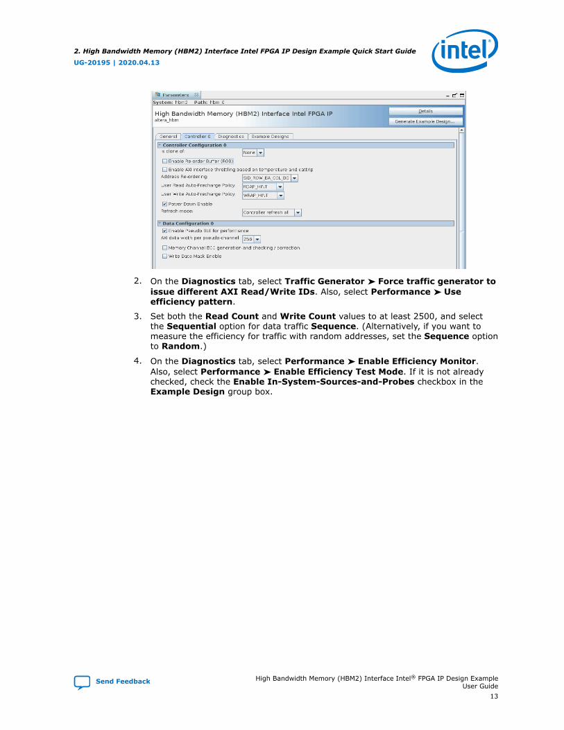
2. On the Diagnostics tab, select Traffic Generator ➤ Force traffic generator toissue different AXI Read/Write IDs. Also, select Performance ➤ Useefficiency pattern.
3. Set both the Read Count and Write Count values to at least 2500, and selectthe Sequential option for data traffic Sequence. (Alternatively, if you want tomeasure the efficiency for traffic with random addresses, set the Sequence optionto Random.)
4. On the Diagnostics tab, select Performance ➤ Enable Efficiency Monitor.Also, select Performance ➤ Enable Efficiency Test Mode. If it is not alreadychecked, check the Enable In-System-Sources-and-Probes checkbox in theExample Design group box.
2. High Bandwidth Memory (HBM2) Interface Intel FPGA IP Design Example Quick Start Guide
UG-20195 | 2020.04.13
Send Feedback High Bandwidth Memory (HBM2) Interface Intel® FPGA IP Design ExampleUser Guide
13
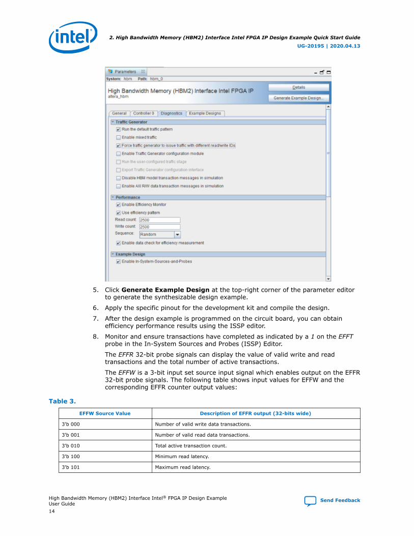
5. Click Generate Example Design at the top-right corner of the parameter editorto generate the synthesizable design example.
6. Apply the specific pinout for the development kit and compile the design.
7. After the design example is programmed on the circuit board, you can obtainefficiency performance results using the ISSP editor.
8. Monitor and ensure transactions have completed as indicated by a 1 on the EFFTprobe in the In-System Sources and Probes (ISSP) Editor.
The EFFR 32-bit probe signals can display the value of valid write and readtransactions and the total number of active transactions.
The EFFW is a 3-bit input set source input signal which enables output on the EFFR32-bit probe signals. The following table shows input values for EFFW and thecorresponding EFFR counter output values:
Table 3.
EFFW Source Value Description of EFFR output (32-bits wide)
3'b 000 Number of valid write data transactions.
3'b 001 Number of valid read data transactions.
3'b 010 Total active transaction count.
3'b 100 Minimum read latency.
3'b 101 Maximum read latency.
2. High Bandwidth Memory (HBM2) Interface Intel FPGA IP Design Example Quick Start Guide
UG-20195 | 2020.04.13
High Bandwidth Memory (HBM2) Interface Intel® FPGA IP Design ExampleUser Guide
Send Feedback
14
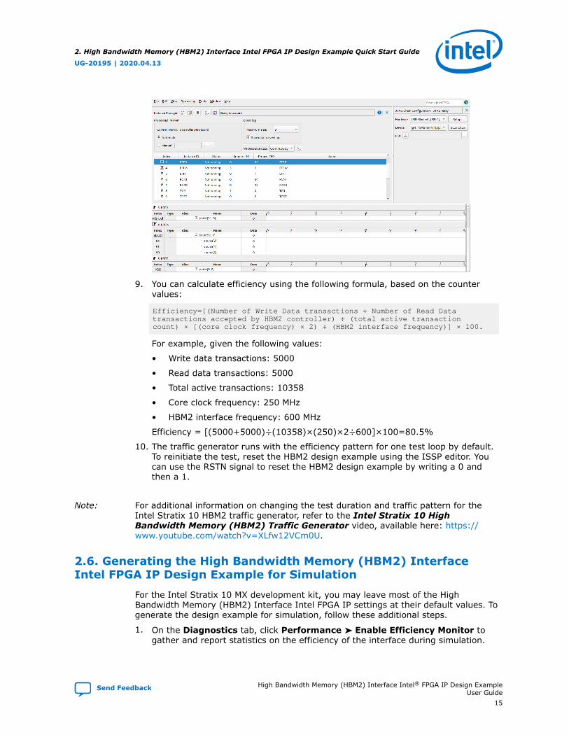
9. You can calculate efficiency using the following formula, based on the countervalues:
Efficiency=[(Number of Write Data transactions + Number of Read Data transactions accepted by HBM2 controller) ÷ (total active transaction count) × [(core clock frequency) × 2) ÷ (HBM2 interface frequency)] × 100.
For example, given the following values:
• Write data transactions: 5000
• Read data transactions: 5000
• Total active transactions: 10358
• Core clock frequency: 250 MHz
• HBM2 interface frequency: 600 MHz
Efficiency = [(5000+5000)÷(10358)×(250)×2÷600]×100=80.5%
10. The traffic generator runs with the efficiency pattern for one test loop by default.To reinitiate the test, reset the HBM2 design example using the ISSP editor. Youcan use the RSTN signal to reset the HBM2 design example by writing a 0 andthen a 1.
Note: For additional information on changing the test duration and traffic pattern for theIntel Stratix 10 HBM2 traffic generator, refer to the Intel Stratix 10 HighBandwidth Memory (HBM2) Traffic Generator video, available here: https://www.youtube.com/watch?v=XLfw12VCm0U.
2.6. Generating the High Bandwidth Memory (HBM2) InterfaceIntel FPGA IP Design Example for Simulation
For the Intel Stratix 10 MX development kit, you may leave most of the HighBandwidth Memory (HBM2) Interface Intel FPGA IP settings at their default values. Togenerate the design example for simulation, follow these additional steps.
1. On the Diagnostics tab, click Performance ➤ Enable Efficiency Monitor togather and report statistics on the efficiency of the interface during simulation.
2. High Bandwidth Memory (HBM2) Interface Intel FPGA IP Design Example Quick Start Guide
UG-20195 | 2020.04.13
Send Feedback High Bandwidth Memory (HBM2) Interface Intel® FPGA IP Design ExampleUser Guide
15

Note: If you enable In-System-Sources-and-Probes, it is instantiated only ifsynthesized by the Intel Quartus Prime software. For simulation, thecorresponding signal is tied to either ground or Vcc.
2. On the Diagnostics tab, click Performance ➤ Use efficiency pattern toprovide high-efficiency concurrent traffic pattern features which are integrated inthe design example. You can configure the different number of read/writetransactions, select between sequential or random traffic addressing, and enableor disable the data-matching check. This option also enables the Read commandround trip latency feature. Latency is measured from the start of read commandvalid by the driver, until the response is received.
3. Ensure that the Simulation checkbox is checked under Example Design Files onthe Example Designs tab.
Note: By default, both the Simulation and Synthesis checkboxes are checked.
2. High Bandwidth Memory (HBM2) Interface Intel FPGA IP Design Example Quick Start Guide
UG-20195 | 2020.04.13
High Bandwidth Memory (HBM2) Interface Intel® FPGA IP Design ExampleUser Guide
Send Feedback
16

4. Click File ➤ Save. The system creates and saves the current settings in the userIP variation file (<user instance name>.ip), within the <user projectdirectory> that you specified.
5. Click Generate Example Design in the top-right corner of the window.
6. Specify a directory for the generated design example (<design exampledirectory>) and click OK. The system creates the following design example filesets within the specified directory:
2. High Bandwidth Memory (HBM2) Interface Intel FPGA IP Design Example Quick Start Guide
UG-20195 | 2020.04.13
Send Feedback High Bandwidth Memory (HBM2) Interface Intel® FPGA IP Design ExampleUser Guide
17

7. To exit the IP Parameter Editor Pro window, click File ➤ Exit.
2.7. Regenerating the High Bandwidth Memory (HBM2) InterfaceIntel FPGA IP Design Example After Modification
If you modify the IP variation files or Platform Designer files in the post-generationsynthesis folder, you can let the Intel Quartus Prime software regenerate the designexample files through the integrated IP regeneration process during the Intel QuartusPrime compilation. Alternatively, you can use the design example's pregeneration filesto view, modify, generate, or regenerate the design example files. The design
2. High Bandwidth Memory (HBM2) Interface Intel FPGA IP Design Example Quick Start Guide
UG-20195 | 2020.04.13
High Bandwidth Memory (HBM2) Interface Intel® FPGA IP Design ExampleUser Guide
Send Feedback
18

example's pregeneration scripts are generated when you click the Generate ExampleDesign button in the IP Parameter Editor Pro window. The pregeneration scripts aregenerated regardless of whether you select the Simulation or Synthesis checkbox.
1. To generate or regenerate the synthesis or simulation file sets, run one of thefollowing scripts:
• To create a project for compilation, run the quartus_sh -tmake_qii_design.tcl script in the destination directory.
• To create a project for simulation, run the quartus_sh -tmake_sim_design.tcl script in the destination directory.
2. High Bandwidth Memory (HBM2) Interface Intel FPGA IP Design Example Quick Start Guide
UG-20195 | 2020.04.13
Send Feedback High Bandwidth Memory (HBM2) Interface Intel® FPGA IP Design ExampleUser Guide
19

3. High Bandwidth Memory (HBM2) Interface Intel FPGAIP Design Example Description
When you parameterize the High Bandwidth Memory (HBM2) Interface Intel FPGA IP,you can have the system generate simulation and synthesis file sets, by selectingSimulation or Synthesis under Example Design Files on the Example Designstab.
The system creates a complete file set for simulation or for synthesis, in accordancewith your selection.
3.1. High Bandwidth Memory (HBM2) Interface Intel FPGA IPSynthesis Design Example
The synthesis design example contains the following major blocks.
• An instance of the High Bandwidth Memory (HBM2) Interface Intel FPGA IP thatmanages the read, write, and other operations to the HBM2 device.
• Two independent traffic generators for every HBM channel enabled (one trafficgenerator for each HBM Pseudo-channel). The traffic generator is a synthesizableAXI-4 type example driver that implements a pseudo-random pattern of reads andwrites to a parameterized number of addresses. The traffic generator alsomonitors the data read from the memory to ensure it matches the written dataand asserts a failure otherwise.
• An I/O PLL to emulate the external core clock that feeds the ext_core_clockport of the HBM2 IP. The clock eventually clocks the Traffic Generator and anyother components that are clocked by the wmc_clk_0_clk clock of the HBM2 IP.
Figure 3. Synthesis Design Example
External CoreClock I/O PLL
Traffic Generator CH0 PC0
Traffic Generator CH0 PC1
High Bandwidth Memory (HBM2) Interface Intel FPGA IP
High Bandwidth Memory
AXI - 4
AXI - 4
ext_core_clk
UIB
Synthesis Design Example
UG-20195 | 2020.04.13
Send Feedback
Intel Corporation. All rights reserved. Agilex, Altera, Arria, Cyclone, Enpirion, Intel, the Intel logo, MAX, Nios,Quartus and Stratix words and logos are trademarks of Intel Corporation or its subsidiaries in the U.S. and/orother countries. Intel warrants performance of its FPGA and semiconductor products to current specifications inaccordance with Intel's standard warranty, but reserves the right to make changes to any products and servicesat any time without notice. Intel assumes no responsibility or liability arising out of the application or use of anyinformation, product, or service described herein except as expressly agreed to in writing by Intel. Intelcustomers are advised to obtain the latest version of device specifications before relying on any publishedinformation and before placing orders for products or services.*Other names and brands may be claimed as the property of others.
ISO9001:2015Registered

If you enable more than one HBM channel, the synthesis design example includes anadditional pair of traffic generators based on how many HBM channels are enabled.Because each HBM channel and HBM pseudo-channel are independent, each of theadditional traffic generators are also independent from one another, althoughconnected to a single High Bandwidth Memory (HBM2) Interface Intel FPGA IP. Thefollowing figure shows an example with HBM channels enabled.
Figure 4. Synthesis Design Example with Three HBM Channels Enabled
External CoreClock I/O PLL
Traffic Generator CH0 PC0
Traffic Generator CH0 PC1
High Bandwidth Memory (HBM2) Interface Intel FPGA IP
High Bandwidth Memory
AXI - 4
AXI - 4
ext_core_clk
UIB
Synthesis Design Example
Traffic Generator CH1 PC0
Traffic Generator CH1 PC1
AXI - 4
AXI - 4
Traffic Generator CH2 PC0
Traffic Generator CH2 PC1
AXI - 4
AXI - 4
Table 4. Top-Level Signals of the HBM2 Design Example
Signal Group Signal Name Direction Width Description
PLL Ref clk Inputs core_clk_iopll_ref_clk_clk
Input 1 LVDS differentialreference clock usedby the I/O PLL togenerate the fabriccore clock. The designexample automaticallyinstantiates the I/OPLL that generates thecore clock.
hbm_0_example_design_pll_ref_clk_clk
Input 1 LVDS differentialreference clock usedby the UIB PLL. Thedesign exampleautomaticallyinstantiates the UIB
continued...
3. High Bandwidth Memory (HBM2) Interface Intel FPGA IP Design Example Description
UG-20195 | 2020.04.13
Send Feedback High Bandwidth Memory (HBM2) Interface Intel® FPGA IP Design ExampleUser Guide
21

Signal Group Signal Name Direction Width Description
PLL that generates theclock for the UIBsubsystem.
Resets core_clk_iopll_reset_reset
Input 1 Reset input for thecore clock I/O PLL.The reset polarity isactive high. Refer tothe Intel Stratix 10device datasheet forI/O PLL specifications.
hbm_0_example_design_wmcrst_n_in_reset_n
Input 1 General core logicreset; active low.
hbm_only_reset_in_reset
Input 1 HBM-only reset; activehigh. Not currentlysupported; you canconnect this to LOW.
Boundary ScanSignals
m2u_bridge_cattrip
Input 1 HBM2 boundarysignals that are notdriven by the trafficgenerator. Thesesignals must beexposed at the designexample top level toenable successfulcompilation. Thesesignals should not beactively driven. TheIntel Quartus Primesoftware places thesesignals on pins thatare connected to theHBM2 memory. Do notadd any locationassignments to thesepins, as doing socauses compilationerrors.
m2u_bridge_temp Input 3
m2u_bridge_wso Input 8
m2u_bridge_reset_n
Output 1
m2u_bridge_wrst_n Output 1
m2u_bridge_wrck Output 1
m2u_bridge_shiftwr
Output 1
m2u_bridge_capturewr
Output 1
m2u_bridge_updatewr
Output 1
m2u_bridge_selectwir
Output 1
m2u_bridge_wsi Output 1
Traffic GeneratorStatus Signals
tgx_0_status_traffic_gen_pass
Output 1 Traffic generatorstatus signals (Pass,Fail and Timeout) forPseudo Channel 0, perChannel.
tgx_0_status_traffic_gen_fail
Output 1
tgx_0_status_traffic_gen_timeout
Output 1
continued...
3. High Bandwidth Memory (HBM2) Interface Intel FPGA IP Design Example Description
UG-20195 | 2020.04.13
High Bandwidth Memory (HBM2) Interface Intel® FPGA IP Design ExampleUser Guide
Send Feedback
22

Signal Group Signal Name Direction Width Description
tgx_1_status_traffic_gen_pass
Output 1 Traffic generatorstatus signals (Pass,Fail and Timeout) forPseudo Channel 1, perChannel.
tgx_1_status_traffic_gen_fail
Output 1
tgx_1_status_traffic_gen_timeout
Output 1
Using the Design Example in a Project with Multiple HBM2 Interfaces
Do not instantiate an HBM2 design example in a project multiple times, because aFitter error may occur.
To create a project with two HBM2 interfaces, create two instances of the HBM2 IP,one with HBM location = Top and one with HBM2 location = bottom. Generate thedesign example projects for each IP and then instantiate them in the multiple HBM2interface project.
Related Information
Intel Stratix 10 Device Datasheet
3.2. High Bandwidth Memory (HBM2) Interface Intel FPGA IPSimulation Design Example
The simulation design example contains the following major blocks.
• The simulation example includes all the major blocks that exist in the synthesisdesign example, including a traffic generator pair, and an instance of the HighBandwidth Memory (HBM2) Interface Intel FPGA IP and external core clock I/OPLL. These blocks default to abstract simulation models where appropriate forrapid simulation. The design example may also include an Efficiency Monitor blockfor every HBM channel that you have enabled. The Efficiency Monitor block reportsthe efficiency number for the particular HBM channel at the end of simulation.
• An HBM2 memory model, which acts as a generic model that conforms to theHBM2 protocol specifications. Frequently, HBM2 vendors provide simulationmodels for their specific HBM2 components that you can download from theirwebsites.
• A simulation checker, which monitors the status signals from the HBM2 IP and thetraffic generator, to signal an overall pass or fail condition.
• The clock source and reset source instances which are the Bus Functional Model(BFM) that generates the reference clock and reset signal.
3. High Bandwidth Memory (HBM2) Interface Intel FPGA IP Design Example Description
UG-20195 | 2020.04.13
Send Feedback High Bandwidth Memory (HBM2) Interface Intel® FPGA IP Design ExampleUser Guide
23

Figure 5. Simulation Design Example with Efficiency Monitor Enabled
External CoreClock I/O PLL
Traffic Generator CH0 PC0
Traffic Generator CH0 PC1
High Bandwidth Memory (HBM2) Interface Intel FPGA IP
HBM2 Memory Model
Simulation Design Example
Core Clock Source
Global Reset Source
AXI - 4
AXI - 4
Simulation Checker
HBM Only Reset Source
EfficiencyMonitor CH0
ext_core_clk
StatusStatus
Status
Memory
Note: Unlike other styles of memory interface where the testbench normally wraps thesynthesis example design top-level file, for the High Bandwidth Memory (HBM2)Interface Intel FPGA IP, the Traffic Generator and other non-High Bandwidth Memory(HBM2) Interface Intel FPGA IP components are instantiated in the top-level testbenchfile.
3.3. High Bandwidth Memory (HBM2) Interface Intel FPGA IPDesign Example Interface tab
You can use the Example Designs tab in the parameter editor to parameterize andgenerate your design examples.
3. High Bandwidth Memory (HBM2) Interface Intel FPGA IP Design Example Description
UG-20195 | 2020.04.13
High Bandwidth Memory (HBM2) Interface Intel® FPGA IP Design ExampleUser Guide
Send Feedback
24

4. High Bandwidth Memory (HBM2) Interface Intel FPGAIP Design Example User Guide Archives
IP versions are the same as the Intel Quartus Prime Design Suite software versions upto v19.1. From Intel Quartus Prime Design Suite software version 19.2 or later, IPshave a new IP versioning scheme.
If an IP core version is not listed, the user guide for the previous IP core versionapplies.
IP Core Version User Guide
19.2.0 High Bandwidth Memory (HBM2) Interface Intel FPGA IP Design Example User Guide
19.1 High Bandwidth Memory (HBM2) Interface Intel FPGA IP Design Example User Guide
18.1.1 High Bandwidth Memory (HBM2) Interface Intel FPGA IP Design Example User Guide
UG-20195 | 2020.04.13
Send Feedback
Intel Corporation. All rights reserved. Agilex, Altera, Arria, Cyclone, Enpirion, Intel, the Intel logo, MAX, Nios,Quartus and Stratix words and logos are trademarks of Intel Corporation or its subsidiaries in the U.S. and/orother countries. Intel warrants performance of its FPGA and semiconductor products to current specifications inaccordance with Intel's standard warranty, but reserves the right to make changes to any products and servicesat any time without notice. Intel assumes no responsibility or liability arising out of the application or use of anyinformation, product, or service described herein except as expressly agreed to in writing by Intel. Intelcustomers are advised to obtain the latest version of device specifications before relying on any publishedinformation and before placing orders for products or services.*Other names and brands may be claimed as the property of others.
ISO9001:2015Registered

5. Document Revision History for the High BandwidthMemory (HBM2) Interface Intel FPGA IP Design ExampleUser Guide
Document Version Intel QuartusPrime Version
IP Version Changes
2020.04.13 20.1 19.4.0 In the HBM2 Design Example Quick Start Guide chapter:• In the Configuring the High Bandwidth Memory (HBM2)
Interface Intel FPGA IP topic, updated the image in step4.
• In the IP Parameter Editor Pro Guidelines for HighBandwidth Memory (HBM2) Interface Intel FPGA IPtopic, modified the third bullet in the description of theGeneral tab.
• In the Generating the Synthesizable High BandwidthMemory (HBM2) Interface Intel FPGA IP Design Exampletopic, updated the image in step 1.
• In the Generating the Synthesizable High BandwidthMemory (HBM2) Interface Intel FPGA IP for HighEfficiency topic, updated the image in step 4.
• In the Generating the High Bandwidth Memory (HBM2)Interface Intel FPGA IP Design Example for Simulationtopic, updated the image with step 1 and the text of step2.
2019.12.12 19.2 19.2.0 Implemented correction to the efficiency example in step 9of the Generating the Synthesizable High BandwidthMemory (HBM2) Interface Intel FPGA IP for High Efficiencytopic.
2019.08.30 19.2 19.2.0 • Added About the High Bandwidth Memory (HBM2)Interface Intel FPGA IP.
• Added Generating the Synthesizable High BandwidthMemory (HBM2) Interface Intel FPGA IP for HighEfficiency topic.
• Added text to step 2 of the Generating the SynthesizableHigh Bandwidth Memory (HBM2) Interface Intel FPGA IPDesign Example topic.
• Added text to step 2 of the Generating the HighBandwidth Memory (HBM2) Interface Intel FPGA IPDesign Example for Simulation topic.
continued...
UG-20195 | 2020.04.13
Send Feedback
Intel Corporation. All rights reserved. Agilex, Altera, Arria, Cyclone, Enpirion, Intel, the Intel logo, MAX, Nios,Quartus and Stratix words and logos are trademarks of Intel Corporation or its subsidiaries in the U.S. and/orother countries. Intel warrants performance of its FPGA and semiconductor products to current specifications inaccordance with Intel's standard warranty, but reserves the right to make changes to any products and servicesat any time without notice. Intel assumes no responsibility or liability arising out of the application or use of anyinformation, product, or service described herein except as expressly agreed to in writing by Intel. Intelcustomers are advised to obtain the latest version of device specifications before relying on any publishedinformation and before placing orders for products or services.*Other names and brands may be claimed as the property of others.
ISO9001:2015Registered

Document Version Intel QuartusPrime Version
IP Version Changes
• Updated the figure in step 4 of Configuring the HighBandwidth Memory (HBM2) Interface Intel FPGA IP.
• Updated the figures in steps 1 and 3 of Generating theSynthesizable High Bandwidth Memory (HBM2) InterfaceIntel FPGA IP Design Example.
• Updated the figures in steps 1 and 3 of Generating theHigh Bandwidth Memory (HBM2) Interface Intel FPGA IPDesign Example for Simulation.
2019.05.03 19.1 19.1 • Modified the Diagnostic description in Table 1, TabParameter Guidelines in the IP Parameter Editor ProGuidelines for High Bandwidth Memory (HBM2) InterfaceIntel FPGA IP topic.
• Updated the Diagnostics tab figure and added a step forusing the Traffic GeneratorUse efficiency patternfeature in the Generating the Synthesizable HighBandwidth Memory (HBM2) Interface Intel FPGA IPDesign Example topic.
• Updated the Diagnostics tab figure and added a step forusing the Traffic GeneratorUse efficiency patternfeature in the Generating the High Bandwidth Memory(HBM2) Interface Intel FPGA IP Design Example forSimulation topic.
• Added High Bandwidth Memory (HBM2) Interface IntelFPGA IP Design Example User Guide Archives chapter.
2018.12.24 18.1.1 18.1.1 Initial release.
5. Document Revision History for the High Bandwidth Memory (HBM2) Interface Intel FPGA IPDesign Example User Guide
UG-20195 | 2020.04.13
Send Feedback High Bandwidth Memory (HBM2) Interface Intel® FPGA IP Design ExampleUser Guide
27