vga signal generation with the xs board - | xess corp. · vga signal generation with the xs board...
TRANSCRIPT

VGA Signal Generation with the XS Board
Aug 25, 1998 (Version 1.0) Application Note by D. Vanden Bout
Summary This memo discusses the timing for the signals that drive a VGA monitor and describes a circuit that will let you drive a monitor with the XS Board.
VGA Color Signals There are three signals -- red, green, and blue -- that send color information to a VGA monitor. These three signals each drive an electron gun that emits electrons which paint one primary color at a point on the monitor screen. Analog levels between 0 (completely dark) and 0.7 V (maximum brightness) on these control lines tell the monitor what intensities of these three primary colors to combine to make the color of a dot (or pixel) on the monitor’s screen.
Each analog color input can be set to one of four levels by two digital outputs using a simple two-bit digital-to-analog converter (see Figure 1). The four possible levels on each analog input are combined by the monitor to create a pixel with one of 4 × 4 × 4 = 64 different colors. So the six digital control lines let us select from a palette of 64 colors.
Figure 1: Digital-to-analog VGA monitor interface.

VGA Signal Timing A single dot of color on a video monitor doesn’t impart much information. A horizontal line of pixels carries a bit more information. But a frame composed of multiple lines can present an image on the monitor screen. A frame of VGA video typically has 480 lines and each line usually contains 640 pixels. In order to paint a frame, there are deflection circuits in the monitor that move the electrons emitted from the guns both left-to-right and top-to-bottom across the screen. These deflection circuits require two synchronization signals in order to start and stop the deflection circuits at the right times so that a line of pixels is painted across the monitor and the lines stack up from the top to the bottom to form an image. The timing for the VGA synchronization signals is shown in Figure 2.
Negative pulses on the horizontal sync signal mark the start and end of a line and ensure that the monitor displays the pixels between the left and right edges of the visible screen area. The actual pixels are sent to the monitor within a 25.17 µs window. The horizontal sync signal drops low a minimum of 0.94 µs after the last pixel and stays low for 3.77 µs. A new line of pixels can begin a minimum of 1.89 µs after the horizontal sync pulse ends. So a single line occupies 25.17 µs of a 31.77 µs interval. The other 6.6 µs of each line is the horizontal blanking interval during which the screen is dark.
In an analogous fashion, negative pulses on a vertical sync signal mark the start and end of a frame made up of video lines and ensure that the monitor displays the lines between the top and bottom edges of the visible monitor screen. The lines are sent to the monitor within a 15.25 ms window. The vertical sync signal drops low a minimum of 0.45 ms after the last line and stays low for 64 µs. The first line of the next frame can begin a minimum of 1.02 ms after the vertical sync pulse ends. So a single frame occupies 15.25 ms of a 16.784 ms interval. The other 1.534 ms of the frame interval is the vertical blanking interval during which the screen is dark.

Figure 2: VGA signal timing.
VGA Signal Generator Algorithm Now we have to figure out a process that will send pixels to the monitor with the correct timing and framing. We can store a picture in the RAM of the XS Board. Then we can retrieve the data from the RAM, format it into lines of pixels, and send the lines to the monitor with the appropriate pulses on the horizontal and vertical sync pulses.
The pseudocode for a single frame of this process is shown in Listing 1. The pseudocode has two outer loops: one which displays the L lines of visible pixels, and another which inserts the V blank lines and the vertical sync pulse. Within the first loop, there are two more loops: one which sends the P pixels of each video line to the monitor, and another which inserts the H blank pixels and the horizontal sync pulse.
Within the pixel display loop, there are statements to get the next byte from the RAM. Each byte contains four two-bit pixels. A small loop iteratively extracts each pixel to be displayed from the lower two bits of the byte. Then the byte is shifted by two bits so the next pixel will be in the right position during the next iteration of the loop. Since it has only two bits, each pixel can store one of four colors. The mapping from the two-bit pixel value to the actual values required by the monitor electronics is done by the COLOR_MAP() routine.

/* send L lines of video to the monitor */ for line_cnt=1 to L /* send P pixels for each line */ for pixel_cnt=1 to P /* get pixel data from the RAM */ data = RAM(address) address = address + 1 /* RAM data byte contains 4 pixels */ for d=1 to 4 /* mask off pixel in the lower two bits */ pixel = data & 00000011 /* shift next pixel into lower two bits */ data = data>>2 /* get the color for the two-bit pixel */ color = COLOR_MAP(pixel) send color to monitor d = d + 1 /* increment by four pixels */ pixel_cnt = pixel_cnt + 4 /* blank the monitor for H pixels */ for horiz_blank_cnt=1 to H color = BLANK send color to monitor /* pulse the horizontal sync at the right time */ if horiz_blank_cnt>HB0 and horiz_blank_cnt<HB1 hsync = 0 else hsync = 1 horiz_blank_cnt = horiz_blank_cnt + 1 line_cnt = line_cnt + 1 /* blank the monitor for V lines and insert vertical sync */ for vert_blank_cnt=1 to V color = BLANK send color to monitor /* pulse the vertical sync at the right time */ if vert_blank_cnt>VB0 and vert_blank_cnt<VB1 vsync = 0 else vsync = 1 vert_blank_cnt = vert_blank_cnt + 1 /* go back to start of picture in RAM */ address = 0
Listing 1: VGA signal generation pseudocode. Figure 3 shows how to pipeline certain operations to account for delays in accessing data from the RAM. The pipeline has three stages:
stage 1: The circuit uses the horizontal and vertical counters to compute the address where the next pixel is found in RAM. The counters are also used to determine the firing of the sync pulses and whether the video should be blanked. The pixel data from the RAM, blanking signal, and sync pulses are latched at the end of this stage so they can be used in the next stage.
stage 2: The circuit uses the pixel data and the blanking signal to determine the binary color outputs. These outputs are latched at the end of this stage.
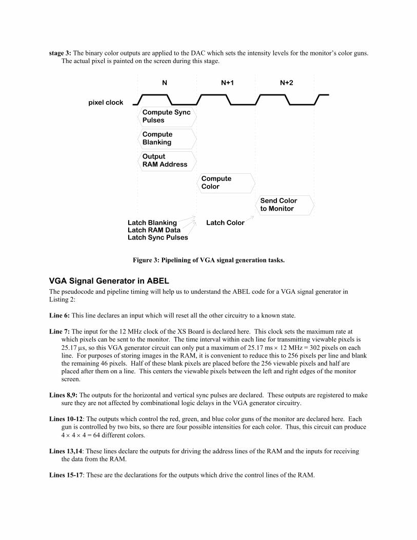
stage 3: The binary color outputs are applied to the DAC which sets the intensity levels for the monitor’s color guns. The actual pixel is painted on the screen during this stage.
Figure 3: Pipelining of VGA signal generation tasks.
VGA Signal Generator in ABEL The pseudocode and pipeline timing will help us to understand the ABEL code for a VGA signal generator in Listing 2:
Line 6: This line declares an input which will reset all the other circuitry to a known state.
Line 7: The input for the 12 MHz clock of the XS Board is declared here. This clock sets the maximum rate at which pixels can be sent to the monitor. The time interval within each line for transmitting viewable pixels is 25.17 µs, so this VGA generator circuit can only put a maximum of 25.17 ms × 12 MHz = 302 pixels on each line. For purposes of storing images in the RAM, it is convenient to reduce this to 256 pixels per line and blank the remaining 46 pixels. Half of these blank pixels are placed before the 256 viewable pixels and half are placed after them on a line. This centers the viewable pixels between the left and right edges of the monitor screen.
Lines 8,9: The outputs for the horizontal and vertical sync pulses are declared. These outputs are registered to make sure they are not affected by combinational logic delays in the VGA generator circuitry.
Lines 10-12: The outputs which control the red, green, and blue color guns of the monitor are declared here. Each gun is controlled by two bits, so there are four possible intensities for each color. Thus, this circuit can produce 4 × 4 × 4 = 64 different colors.
Lines 13,14: These lines declare the outputs for driving the address lines of the RAM and the inputs for receiving the data from the RAM.
Lines 15-17: These are the declarations for the outputs which drive the control lines of the RAM.

Lines 19,20: The counters that store the current horizontal position within a line of pixels and the vertical position of the line on the screen are declared on these lines. We will call these the horizontal or pixel counter, and the vertical or line counter, respectively. The line period is 31.77 µs which is 381 clock cycles, so the pixel counter needs at least nine bits of resolution. Each frame is composed of 528 video lines (only 480 are visible, the other 48 are blanked), so a ten bit counter is needed for the line counter.
Line 21: This is the declaration for the eight-bit register that stores the four pixels received from the RAM.
Lines 22,23: This line declares the video blanking signal and its registered counterpart that is used in the next pipeline stage.
Lines 25-31: These lines define aliases for the signals that were declared earlier. Not that the current active pixel is defined to be in the lower two bits of the pixel byte.
Line 35: The length of carry lookahead is set to one position, so all adders that follow will be of the simple, space-efficient ripple-carry type. This conserves logic gates at the expense of speed.
Lines 37,38: The pixel and line counters are set to zero when the reset input is high. The reset is only activated at the start of the operation of the VGA generator circuitry and is not used during the normal operations.
Lines 39,40: The pixel counter is incremented on the rising edge of the 12 MHz pixel clock. The vertical line counter is clocked by the rising edge of the horizontal blanking pulse, so it increments only after a line of pixels is completed.
Lines 42,43: The active-low horizontal and vertical sync registers are set to high values when the reset input is high.
Lines 44,45: The registered horizontal sync output is updated on every pixel clock. The registered vertical sync output is updated whenever a line of video is completed. The values that are placed in these registers at specific times are determined in the statements which follow.
Line 48: This line sets the range for the horizontal pixel counter to be [0,380]. When the counter reaches 380, it rolls over to 0. Thus, the counter has a period of 381 pixel clocks. With a pixel clock of 12 MHz, this translates to a period of 31.75 µs.
Line 50: This line determines the active and inactive intervals of the registered horizontal sync output. The sync signal goes low on the cycle after the pixel counter reaches 291 and continues until the cycle after the counter reaches 337. This gives a low horizontal sync pulse of (337-291)=46 pixel clocks. With a pixel clock of 12 MHz, this translates to a low-going horizontal sync pulse of 3.83 µs. The sync pulse starts 292 clocks after the line of pixels begins, which translates to 24.33 µs. This is less than the 26.11 µs we stated before. The difference of 1.78 ms translates to 21 pixel clocks. This time interval corresponds to the 23 blank pixels that are placed prior to the 256 viewable pixels (minus two clock cycles for pipelining delays).
Line 52: This line sets the range for the vertical line counter to be [0,527]. When the counter reaches 527, it rolls over to 0. Thus, the counter has a period of 528 lines. Since the duration of a line of pixels is 31.75 µs, this makes the frame interval equal to 16.76 ms.
Line 54: This line determines the active and inactive intervals of the registered vertical sync output. The sync signal goes low on the cycle after the line counter reaches 493 and continues until the cycle after the counter reaches 495. This gives a low vertical sync pulse of (495-493)= 2 lines. With a line interval of 31.75 µs, this translates to a low-going vertical sync pulse of 63.5 µs. The vertical sync pulse starts 494 × 31.75 µs = 15.68 ms after the beginning of the first video line.
Line 56: The activation of the video blanking control signal is set on this line. The video is blanked after 256 pixels on a line are displayed, or after 480 lines are displayed.

Lines 58-60: The blanking signal is stored in a register so it can be used during the next stage of the pipeline when the color is computed.
Lines 63,64: On these lines, the RAM is permanently selected and writing to the RAM is disabled. This makes the RAM look like a ROM which stores video data.
Line 65: The outputs from the RAM are disabled when the video is blanked since there is no need for pixels during the blanking intervals. This isn’t really necessary since no other circuit is trying to access the RAM.
Line 71: The address in RAM where the next four pixels are stored is calculated by concatenating the lower nine bits of the line counter with bits 7,6,5,4,3 and 2 of the pixel counter. With this arrangement, the line counter stores the address of one of 29 = 512 pages. Each page contains 26 = 64 bytes. Each byte contains four pixels, so each page stores one line of 256 pixels. The pixel counter increments through the bytes of a page to get the pixels for the current line. (Note that we don’t need to use bits 1 and 0 of the pixel counter when computing the RAM address since each byte contains four pixels.) After the line is displayed, the line counter is incremented to point to the next page.
Lines 73,74: The register that holds the byte of pixel data from RAM is cleared when the VGA circuit is reset. The register is updated on the rising edge of each pixel clock.
Lines 80-82: The pixel register is loaded with data from the RAM whenever the lowest two bits of the pixel counter are both zero. The active pixel is always in the lower two bits of the register. Each pixel in the RAM data byte is shifted into the active position by right shifting the register two bits on each rising clock edge.
Line 86: The register that holds the red, green, and blue color gun control bits is set to zero when the reset input is high.
Line 87: The color register is clocked on the rising edge of the pixel clock since this is the rate at which new pixel values arrive.
Lines 88-96: This truth-table defines the color gun control bits which are stored in the color register as a function of the pixel value and the blanking input. When the pipelined blanking input is low (lines 87-90), the color displayed on the monitor is red, green, blue, or white depending upon whether the pixel value is 00, 01, 10, or 11, respectively. When the pipelined blanking input is high (lines 91-94), the color register is loaded with zero which will display the color black on the monitor.

001- MODULE VGACORE 002- TITLE 'VGA signal generator core' 003- 004- DECLARATIONS 005- "------ external signals ------- 006- reset PIN; "reset 007- clock PIN; "VGA dot clock 008- hsyncb PIN ISTYPE 'REG'; "horizontal sync 009- vsyncb PIN ISTYPE 'REG'; "vertical (frame) sync 010- red1..red0 PIN ISTYPE 'REG'; "red component 011- green1..green0 PIN ISTYPE 'REG'; "green component 012- blue1..blue0 PIN ISTYPE 'REG'; "blue component 013- addr14..addr0 PIN; "address into video RAM 014- data7..data0 PIN; "data from video RAM 015- csb PIN; "video RAM chip select 016- oeb PIN; "video RAM output enable 017- web PIN; "video RAM write enable 018- "------ internal storage and signals ------- 019- hcnt8..hcnt0 NODE ISTYPE 'REG'; "horizontal pixel counter 020- vcnt9..vcnt0 NODE ISTYPE 'REG'; "vertical line counter 021- pixrg7..pixrg0 NODE ISTYPE 'REG'; "byte-wide register for 4 pixels 022- blank NODE ISTYPE 'COM'; "video blanking signal 023- pblank NODE ISTYPE 'REG'; "pipelined blanking signal 024- "------ synonyms for various items ------- 025- hcnt = [hcnt8..hcnt0]; 026- vcnt = [vcnt9..vcnt0]; 027- vram_addr = [addr14..addr0]; 028- vram_data = [data7..data0]; 029- pixrg = [pixrg7..pixrg0]; 030- pixel = [pixrg1..pixrg0]; " current active 2-bit pixel 031- rgb = [red1..red0,green1..green0,blue1..blue0]; 032- 033- EQUATIONS 034- 035- @CARRY 1; " ripple-carry addition is fast enough 036- 037- hcnt.ACLR = reset; "clear counter on active-high reset 038- vcnt.ACLR = reset; "clear counter on active-high reset 039- hcnt.CLK = clock; "horz. pixel counter increments on each dot clock 040- vcnt.CLK = hsyncb; "line counter increments after every horiz. line 041- 042- hsyncb.ASET = reset; 043- vsyncb.ASET = reset; 044- hsyncb.CLK = clock; 045- vsyncb.CLK = hsyncb; 046- 047- "horiz. pixel counter rolls-over after 381 pixels 048- WHEN (hcnt<380) THEN hcnt:=hcnt+1 ELSE hcnt:=0; 049- "horiz. sync is low during this interval to signal start of a new line 050- WHEN ((hcnt>=291)&(hcnt<337)) THEN hsyncb:=0 ELSE hsyncb:=1; 051- "vertical line counter rolls-over after 528 lines 052- WHEN (vcnt<527) THEN vcnt:=vcnt+1 ELSE vcnt:=0; 053- "vert sync is low during this interval to signal the start of a frame 054- WHEN ((vcnt>=490)&(vcnt<492)) THEN vsyncb:=0 ELSE vsyncb:=1; 055- "blank video outside of visible region: (0,0)->(255,479) 056- WHEN ((hcnt>=256)#(vcnt>=480)) THEN blank=1 ELSE blank=0; 057- "store the blanking signal for use in the next pipeline stage

058- pblank.ACLR = reset; 059- pblank.CLK = clock; 060- pblank := blank; 061- 062- "video RAM control signals 063- csb = 0; "enable the RAM 064- web = 1; "disable writing to the RAM 065- oeb = blank; "enable the RAM outputs when video is not blanked 066- "the video RAM address is built from the lower 9 bits of the vertical 067- "line counter and bits 7-2 of the horizontal column counter. 068- "Each byte of the RAM contains four 2-bit pixels. As an example, 069- "the byte at address ^h1234=^b0001,0010,0011,0100 contains the pixels 070- "at (row,col) of (^h048,^hD0),(^h048,^hD1),(^h048,^hD2),(^h048,^hD3). 071- vram_addr = [vcnt8..vcnt0,hcnt7..hcnt2]; 072- 073- pixrg.ACLR = reset; "clear pixel register on reset 074- pixrg.CLK = clock; "pixel clock controls changes in pixel register 075- "the pixel register is loaded with the byte from the video RAM location 076- "when the lower two bits of the horizontal counter are both zero. 077- "The active pixel is in the lower two bits of the pixel register. 078- "For the next 3 clocks, the pixel register is right-shifted by two bits 079- "to bring the other pixels in the register into the active position. 080- WHEN ([hcnt1..hcnt0]==^b00) 081- THEN pixrg := vram_data "load 4 pixels from RAM 082- ELSE pixrg := [0,0,pixrg7..pixrg2]; "right-shift pixel register 2 bits 083- 084- "color mapper that translates each 2-bit pixel into a 6-bit RGB value. 085- "when the video signal is blanked, the RGB value is forced to 0. 086- rgb.ACLR = reset; 087- rgb.CLK = clock; 088- TRUTH_TABLE ([pblank, pixel] :> rgb) 089- [ 0 ,^b00 ] :> ^b110000; 090- [ 0 ,^b01 ] :> ^b001100; 091- [ 0 ,^b10 ] :> ^b000011; 092- [ 0 ,^b11 ] :> ^b111111; 093- [ 1 ,^b00 ] :> ^b000000; 094- [ 1 ,^b01 ] :> ^b000000; 095- [ 1 ,^b10 ] :> ^b000000; 096- [ 1 ,^b11 ] :> ^b000000; 097- 098- END VGACORE
Listing 2: ABEL code for a VGA signal generator.

The embedding of the VGA generator circuit within a schematic is shown in Figure 4. The user-constraints files for the XS40 and XS95 Boards are shown in Listing 3 and Listing 4, respectively.
Figure 4: Placing the ABEL VGA generator into a schematic.

001- NET RESET LOC=P44; 002- NET CLOCK LOC=P13; 003- NET ADDR<0> LOC=P3; 004- NET ADDR<1> LOC=P4; 005- NET ADDR<2> LOC=P5; 006- NET ADDR<3> LOC=P78; 007- NET ADDR<4> LOC=P79; 008- NET ADDR<5> LOC=P82; 009- NET ADDR<6> LOC=P83; 010- NET ADDR<7> LOC=P84; 011- NET ADDR<8> LOC=P59; 012- NET ADDR<9> LOC=P57; 013- NET ADDR<10> LOC=P51; 014- NET ADDR<11> LOC=P56; 015- NET ADDR<12> LOC=P50; 016- NET ADDR<13> LOC=P58; 017- NET ADDR<14> LOC=P60; 018- NET DATA<0> LOC=P41; 019- NET DATA<1> LOC=P40; 020- NET DATA<2> LOC=P39; 021- NET DATA<3> LOC=P38; 022- NET DATA<4> LOC=P35; 023- NET DATA<5> LOC=P81; 024- NET DATA<6> LOC=P80; 025- NET DATA<7> LOC=P10; 026- NET CS_ LOC=P65; 027- NET OE_ LOC=P61; 028- NET WE_ LOC=P62; 029- NET HSYNC_ LOC=P19; 030- NET VSYNC_ LOC=P67; 031- NET RGB<4> LOC=P23; 032- NET RGB<5> LOC=P18; 033- NET RGB<2> LOC=P24; 034- NET RGB<3> LOC=P20; 035- NET RGB<0> LOC=P25; 036- NET RGB<1> LOC=P26; 037- NET RST LOC=P36; 038- NET XTAL1 LOC=P37;
Listing 3: User-constraints file for the XS40 Board VGA generator circuit.

001- NET RESET LOC=PIN46; 002- NET CLOCK LOC=PIN9; 003- NET ADDR<0> LOC=PIN75; 004- NET ADDR<1> LOC=PIN79; 005- NET ADDR<2> LOC=PIN82; 006- NET ADDR<3> LOC=PIN84; 007- NET ADDR<4> LOC=PIN1; 008- NET ADDR<5> LOC=PIN3; 009- NET ADDR<6> LOC=PIN83; 010- NET ADDR<7> LOC=PIN2; 011- NET ADDR<8> LOC=PIN58; 012- NET ADDR<9> LOC=PIN56; 013- NET ADDR<10> LOC=PIN54; 014- NET ADDR<11> LOC=PIN55; 015- NET ADDR<12> LOC=PIN53; 016- NET ADDR<13> LOC=PIN57; 017- NET ADDR<14> LOC=PIN61; 018- NET DATA<0> LOC=PIN44; 019- NET DATA<1> LOC=PIN43; 020- NET DATA<2> LOC=PIN41; 021- NET DATA<3> LOC=PIN40; 022- NET DATA<4> LOC=PIN39; 023- NET DATA<5> LOC=PIN37; 024- NET DATA<6> LOC=PIN36; 025- NET DATA<7> LOC=PIN35; 026- NET CS_ LOC=PIN65; 027- NET OE_ LOC=PIN62; 028- NET WE_ LOC=PIN63; 029- NET HSYNC_ LOC=PIN15; 030- NET VSYNC_ LOC=PIN24; 031- NET RGB<4> LOC=PIN18; 032- NET RGB<5> LOC=PIN14; 033- NET RGB<2> LOC=PIN19; 034- NET RGB<3> LOC=PIN17; 035- NET RGB<0> LOC=PIN21; 036- NET RGB<1> LOC=PIN23; 037- NET RST LOC=PIN45; 038- NET XTAL1 LOC=PIN10;
Listing 4: User-constraints file for the XS95 Board VGA generator circuit.

VGA Signal Generator in VHDL A VHDL version of the VGA signal generator is shown in Listing 5. The inputs and outputs of the circuit as defined in the entity declaration are as follows:
reset: This line declares an input which will reset all the other circuitry to a known state.
clock: The input for the 12 MHz clock of the XS Board is declared here. This clock sets the maximum rate at which pixels can be sent to the monitor. The time interval within each line for transmitting viewable pixels is 25.17 µs, so this VGA generator circuit can only put a maximum of 25.17 ms × 12 MHz = 302 pixels on each line. For purposes of storing images in the RAM, it is convenient to reduce this to 256 pixels per line and blank the remaining 46 pixels. Half of these blank pixels are placed before the 256 viewable pixels and half are placed after them on a line. This centers the viewable pixels between the left and right edges of the monitor screen.
hsyncb, vsyncb: The outputs for the horizontal and vertical sync pulses are declared. The hsyncb output is declared as a buffer because it will also be referenced within the architecture section as a clock for the vertical line counter.
rgb: The outputs which control the red, green, and blue color guns of the monitor are declared here. Each gun is controlled by two bits, so there are four possible intensities for each color. Thus, this circuit can produce 4 × 4 × 4 = 64 different colors.
addr, data: These lines declare the outputs for driving the address lines of the RAM and the inputs for receiving the data from the RAM.
csb, oeb, web: These are the declarations for the outputs which drive the control lines of the RAM.
The preamble of the architecture section declares the following resources:
hcnt, vcnt: The counters that store the current horizontal position within a line of pixels and the vertical position of the line on the screen are declared on these lines. We will call these the horizontal or pixel counter, and the vertical or line counter, respectively. The line period is 31.77 µs which is 381 clock cycles, so the pixel counter needs at least nine bits of resolution. Each frame is composed of 528 video lines (only 480 are visible, the other 48 are blanked), so a ten bit counter is needed for the line counter.
pixrg: This is the declaration for the eight-bit register that stores the four pixels received from the RAM.
blank, pblank: This line declares the video blanking signal and its registered counterpart that is used in the next pipeline stage.
Within the main body of the architecture section, the following processes are executed:
A: This process describes the operation of the horizontal pixel counter. The counter is asynchronously set to zero when the reset input is high. The counter increments on the rising edge of each pixel clock. The range for the horizontal pixel counter is [0,380]. When the counter reaches 380, it rolls over to 0 on the next cycle. Thus, the counter has a period of 381 pixel clocks. With a pixel clock of 12 MHz, this translates to a period of 31.75 µs.
B: This process describes the operation of the vertical line counter. The counter is asynchronously set to zero when the reset input is high. The counter increments on the rising edge of the horizontal sync pulse after a line of pixels is completed. The range for the horizontal pixel counter is [0,527]. When the counter reaches 527, it rolls over to 0 on the next cycle. Thus, the counter has a period of 528 lines. Since the duration of a line of pixels is 31.75 µs, this makes the frame interval equal to 16.76 ms.

C: This process describes the operation of the horizontal sync pulse generator. The horizontal sync is set to its inactive high level when the reset is activated. During normal operations, the horizontal sync output is updated on every pixel clock. The sync signal goes low on the cycle after the pixel counter reaches 291 and continues until the cycle after the counter reaches 337. This gives a low horizontal sync pulse of (337-291)=46 pixel clocks. With a pixel clock of 12 MHz, this translates to a low-going horizontal sync pulse of 3.83 µs. The sync pulse starts 292 clocks after the line of pixels begins, which translates to 24.33 µs. This is less than the 26.11 µs we stated before. The difference of 1.78 ms translates to 21 pixel clocks. This time interval corresponds to the 23 blank pixels that are placed prior to the 256 viewable pixels (minus two clock cycles for pipelining delays).
D: This process describes the operation of the vertical sync pulse generator. The vertical sync is set to its inactive high level when the reset is activated. During normal operations, the vertical sync output is updated after every line of pixels is completed. The sync signal goes low on the cycle after the line counter reaches 493 and continues until the cycle after the counter reaches 495. This gives a low vertical sync pulse of (495-493)= 2 lines. With a line interval of 31.75 µs, this translates to a low-going vertical sync pulse of 63.5 µs. The vertical sync pulse starts 494 × 31.75 µs = 15.68 ms after the beginning of the first video line.
E: This line describes the computation of the combinatorial blanking signal. The video is blanked after 256 pixels on a line are displayed, or after 480 lines are displayed.
F: This process describes the operation of the pipelined video blanking signal. Within the process, the blanking signal is stored in a register so it can be used during the next stage of the pipeline when the color is computed.
G: On these lines, the RAM is permanently selected and writing to the RAM is disabled. This makes the RAM look like a ROM which stores video data. Also the outputs from the RAM are disabled when the video is blanked since there is no need for pixels during the blanking intervals. This isn’t really necessary since no other circuit is trying to access the RAM.
H: The address in RAM where the next four pixels are stored is calculated by concatenating the lower nine bits of the line counter with bits 7,6,5,4,3 and 2 of the pixel counter. With this arrangement, the line counter stores the address of one of 29 = 512 pages. Each page contains 26 = 64 bytes. Each byte contains four pixels, so each page stores one line of 256 pixels. The pixel counter increments through the bytes of a page to get the pixels for the current line. (Note that we don’t need to use bits 1 and 0 of the pixel counter when computing the RAM address since each byte contains four pixels.) After the line is displayed, the line counter is incremented to point to the next page.
I: This process describes the operation of the register that holds the byte of pixel data read from RAM. The register is asynchronously cleared when the VGA circuit is reset. The register is updated on the rising edge of each pixel clock. The pixel register is loaded with data from the RAM whenever the lowest two bits of the pixel counter are both zero. The active pixel is always in the lower two bits of the register. Each pixel in the RAM data byte is shifted into the active position by right shifting the register two bits on each rising clock edge.
J: this process describes the process by which the current active pixel is mapped into the six bits which drive the red, green and blue color guns. The register is set to zero (which displays as the color black) when the reset input is high. The color register is clocked on the rising edge of the pixel clock since this is the rate at which new pixel values arrive. The value clocked into the register is a function of the pixel value and the blanking input. When the pipelined blanking input is low (inactive), the color displayed on the monitor is red, green, blue, or white depending upon whether the pixel value is 00, 01, 10, or 11, respectively. When the pipelined blanking input is high, the color register is loaded with zero (black).

library IEEE; use IEEE.std_logic_1164.all; use IEEE.std_logic_unsigned.all; entity vgacore is port ( reset: in std_logic; -- reset clock: in std_logic; -- VGA dot clock hsyncb: buffer std_logic; -- horizontal (line) sync vsyncb: out std_logic; -- vertical (frame) sync rgb: out std_logic_vector(5 downto 0); -- red,green,blue colors addr: out std_logic_vector(14 downto 0); -- address to video RAM data: in std_logic_vector(7 downto 0); -- data from video RAM csb: out std_logic; -- video RAM chip enable oeb: out std_logic; -- video RAM output enable web: out std_logic -- video RAM write enable ); end vgacore; architecture vgacore_arch of vgacore is signal hcnt: std_logic_vector(8 downto 0); -- horizontal pixel counter signal vcnt: std_logic_vector(9 downto 0); -- vertical line counter signal pixrg: std_logic_vector(7 downto 0); -- byte register for 4 pixels signal blank: std_logic; -- video blanking signal signal pblank: std_logic; -- pipelined video blanking signal begin A: process(clock,reset) begin -- reset asynchronously clears pixel counter if reset='1' then hcnt <= "000000000"; -- horiz. pixel counter increments on rising edge of dot clock elsif (clock'event and clock='1') then -- horiz. pixel counter rolls-over after 381 pixels if hcnt<380 then hcnt <= hcnt + 1; else hcnt <= "000000000"; end if; end if; end process; B: process(hsyncb,reset) begin -- reset asynchronously clears line counter if reset='1' then vcnt <= "0000000000"; -- vert. line counter increments after every horiz. line elsif (hsyncb'event and hsyncb='1') then -- vert. line counter rolls-over after 528 lines if vcnt<527 then vcnt <= vcnt + 1; else vcnt <= "0000000000"; end if;

end if; end process; C: process(clock,reset) begin -- reset asynchronously sets horizontal sync to inactive if reset='1' then hsyncb <= '1'; -- horizontal sync is recomputed on the rising edge of every dot clock elsif (clock'event and clock='1') then -- horiz. sync low in this interval to signal start of new line if (hcnt>=291 and hcnt<337) then hsyncb <= '0'; else hsyncb <= '1'; end if; end if; end process; D: process(hsyncb,reset) begin -- reset asynchronously sets vertical sync to inactive if reset='1' then vsyncb <= '1'; -- vertical sync is recomputed at the end of every line of pixels elsif (hsyncb'event and hsyncb='1') then -- vert. sync low in this interval to signal start of a new frame if (vcnt>=490 and vcnt<492) then vsyncb <= '0'; else vsyncb <= '1'; end if; end if; end process; -- blank video outside of visible region: (0,0) -> (255,479) E: blank <= '1' when (hcnt>=256 or vcnt>=480) else '0'; -- store the blanking signal for use in the next pipeline stage F: process(clock,reset) begin if reset='1' then pblank <= '0'; elsif (clock'event and clock='1') then pblank <= blank; end if; end process; -- video RAM control signals G: csb <= '0'; -- enable the RAM web <= '1'; -- disable writing to the RAM oeb <= blank; -- enable the RAM outputs when video is not blanked -- The video RAM address is built from the lower 9 bits of the vertical -- line counter and bits 7-2 of the horizontal pixel counter. -- Each byte of the RAM contains four 2-bit pixels. As an example, -- the byte at address ^h1234=^b0001,0010,0011,0100 contains the pixels

-- at (row,col) of (^h048,^hD0),(^h048,^hD1),(^h048,^hD2),(^h048,^hD3). H: addr <= vcnt(8 downto 0) & hcnt(7 downto 2); I: process(clock,reset) begin -- clear the pixel register on reset if reset='1' then pixrg <= "00000000"; -- pixel clock controls changes in pixel register elsif (clock'event and clock='1') then -- the pixel register is loaded with the contents of the video -- RAM location when the lower two bits of the horiz. counter -- are both zero. The active pixel is in the lower two bits -- of the pixel register. For the next 3 clocks, the pixel -- register is right-shifted by two bits to bring the other -- pixels in the register into the active position. if hcnt(1 downto 0)="00" then pixrg <= data; -- load 4 pixels from RAM else pixrg <= "00" & pixrg(7 downto 2); -- right-shift pixel register end if; end if; end process; -- the color mapper translates each 2-bit pixel into a 6-bit -- color value. When the video signal is blanked, the color -- is forced to zero (black). J: process(clock,reset) begin -- blank the video on reset if reset='1' then rgb <= "000000"; -- update the color outputs on every dot clock elsif (clock'event and clock='1') then -- map the pixel to a color if the video is not blanked if pblank='0' then case pixrg(1 downto 0) is when "00" => rgb <= "110000"; -- red when "01" => rgb <= "001100"; -- green when "10" => rgb <= "000011"; -- blue when others => rgb <= "111111"; -- white end case; -- otherwise, output black if the video is blanked else rgb <= "000000"; -- black end if; end if; end process; end vgacore_arch;
Listing 5: VHDL code for a VGA signal generator.

The embedding of the VGA generator circuit within a schematic is shown in Figure 5. (The CSB and WEB outputs of the VGACORE macro are static. Foundation reported an error when they were connected to the OBUF buffers for the CS_ and WE_ outputs. Therefore, I explicitly tied the buffer inputs to the appropriate levels and left the macro outputs unconnected.) The user-constraints files for the XS40 and XS95 Boards are unchanged from the ABEL design of the previous section and are shown in Listing 3 and Listing 4, respectively.
Figure 5: Placing the VHDL VGA generator into a schematic.