vibrational properties of low-dimensional inorganic
TRANSCRIPT

Vibrational properties of
low-dimensional inorganic layered materials
vorgelegt vonDiplom-PhysikerMatthias Staiger
geboren in Filderstadt
von der Fakultät II - Mathematik und Naturwissenschaftender Technischen Universität Berlin
zur Erlangung des akademischen Grades
Doktor der NaturwissenschaftenDr. rer. nat.
genehmigte Dissertation
Promotionsausschuss:
Vorsitzender: Prof. Dr. Michael LehmannGutachter: Prof. Dr. Christian Thomsen
PD Dr. Tobias Korn
Tag der wissenschaftlichen Aussprache: 27.02.2017
Berlin 2017


Abstract
The family of low-dimensional inorganic layered materials covers a wide spectrum of properties,structurally and electronically. Ever since their synthesis as nanotubes and their preparation asmono- and few-layers these inorganic analogues to carbon nanotubes and graphene, respectively,have attracted a lot of interest both because of their importance for fundamental research aswell as for their potential use in nanoelectronic applications.In this thesis I aimed to get insight into the vibrational and electronic properties of low-dimensional transition metal dichalcogenides and their intercalation in misfit layer compounds.The experimental method of choice was Raman and Resonance Raman spectroscopy and re-search was greatly supported by electron microscopy characterization that allowed me to haveprecise structural information prior to Raman measurements. Case studies were performed onquasi zero-dimensional MoS2 inorganic fullerene-like structures, quasi one-dimensional WS2 andSnS2 nanotubes, on quasi two-dimensional WS2 and MoS2 mono- and few-layers as well as on theintercalation and misfit layer PbNbS2, SnS-SnS2 and (PbS)1.14NbS2 nanotubes where bound-aries between the different dimensionalities become blurred.Despite the variety of materials, the Raman spectroscopic investigations performed in this the-sis made evident that there are a few recurring fingerprint Raman features that allow to drawconclusions about the vibrational and electronic properties far beyond the focus of the casestudies. Looking at the main out-of-plane mode in particular, by recording Resonance Ramanprofiles in the region of the A exciton, I was able to show for WS2 nanotubes how the nanotubediameter affects the first optical transition energies by virtue of the changes in nanotube cur-vature with diameter. The Raman intensity ratio of a sideband to the out-of-plane mode wasfollowed for different excitation energies and pressure and temperature changes and its devel-opment was proven to be due to slightly different resonance conditions of the two modes. Thesame out-of-plane mode and its sidebands were the main subject of my work on few-layer WS2where I established experimentally a “N modes for N layers” rule. I was able to trace backthe appearance of formally infrared-active modes in the Raman spectra to the peculiar in-planeorientation of the A excitonic wavefunction in group VIB transition metal dichalcogenides.In the investigated intercalation and misfit layer compounds the Raman features were shown tobe composed of a superposition of Raman modes of their constituents. Here, the main out-of-plane mode was observed to barely change in comparison with the respective parent material.Instead, in PbNbS2 and (PbS)1.14NbS2 nanotubes the in-plane modes were at the center of theRaman studies and seen to shift up drastically. The underlying reason for these shifts has tobe found in the nature and strength of interlayer interactions and a range of mechanisms isdiscussed in the last part of my thesis. I was able to refute some of the common beliefs in tryingto explain the unusual frequency shifts. I developed an approach that looks at the redistributionof charges in the intercalant layer during the vibrational displacement of atoms in the transitionmetal dichalcogenide layer that can serve as an alternative explanation for the hitherto unex-plained phenomenon.
iii

KurzfassungZiel der vorliegenden Dissertation war es, genauere Einblicke in die Schwingungs- und elektron-ischen Eigenschaften niederdimensionaler Übergangsmetalldichalkogenide und aus ihnen gebilde-ter Misfitmaterialien zu erlangen. Dazu wurde als experimentelle Methode die Raman- undResonanz-Raman-Spektroskopie gewählt, wobei die genaue elektronenmikroskopische Charak-terisierung der Materialien vor der Aufnahme von Ramanspektren einen wesentlichen Teil amForschungserfolg hatte. Als Fallstudien dienten quasi-nulldimensionale fullerenähnliche Struk-turen aus Molybdändisulfid, quasi-eindimensionale WS2- und SnS2-Nanoröhren, quasi-zwei-dimensionale ein- und weniglagige Schichten aus Wolfram- und Molybdändisulfid sowie Dichalko-genidnanoröhren mit eingelagerten Atomen und in Form von Misfitschichten wie PbNbS2, SnS-SnS2 und (PbS)1.14NbS2, bei denen die Grenzen zwischen den Dimensionalitäten verschwimmen.Trotz der großen Bandbreite an untersuchten Materialien brachten die Ramanspektrokopis-chen Untersuchungen zutage, dass sich mit der Untersuchung einiger weniger wiederkehrendercharakteristischer Ramanmoden weitreichende Aussagen über die Schwingungs- und elektro-nischen Eigenschaften treffen lassen. Einer Ramanmode, in der die Schwefelatome aus derLagenebene herausschwingen (out-of-plane) galt besonderes Augenmerk: Bei der Analyse vonResonanz-Raman-Profilen von WS2-Nanoröhren verschiedenen Durchmessers konnte ich zeigen,auf welche Weise die Dicke der Nanoröhren Auswirkungen auf die Energie der ersten optis-chen Übergänge hat und die Abhängigkeit auf die unterschiedliche Stärke der Kurvatur in deneinzelnen Nanoröhrenlagen zurückführen. Desweiteren gelang es mir nachzuweisen, dass dieVeränderung der relativen Intensität einer Nachbarmode zur eben beschriebenen Hauptmode inAbhängigkeit von Anregungsenergie, Temperatur und Druck jeweils der Tatsache geschuldet ist,dass für die benachbarten Moden in Nanoröhren leicht unterschiedliche Resonanzbedingungengelten. Dieselbe Haupt- und Seitenmode lag im Fokus meiner Arbeit an weniglagigem WS2,bei der ich eine „N Moden für N Lagen“-Regel etablieren konnte. Es gelang mir das Auf-tauchen formal infrarotaktiver Moden in den Ramanspektren durch die besondere Orientierungder Wellenfunktion des A-Exzitons in der Ebene der WS2-Lagen zu erklären.Die Ramanmoden in den untersuchten Misfitmaterialien setzen sich aus einer Überlagerung derSchwingungsmoden der einzelnen Materialbausteine zusammen. Während sich die out-of-plane-Mode in den Kompositmaterialien im Vergleich zu dem jeweiligen Elternmaterial kaum verän-dert zeigte, galt das Augenmerk hier den in-plane-Moden, bei denen die Schwingungsrichtungder Schwefelatome innerhalb der Lagenebene liegt. Speziell in PbNbS2- und (PbS)1.14NbS2-Nanoröhren konnte ich eine drastische Erhöhung der Ramanfrequenz im Vergleich zu NbS2feststellen. Der zu Grunde liegende Mechanismus für das ungewöhnlich starke Ausmaß der Ver-schiebung ist in der Stärke und der Natur der elektronischen Wechselwirkung der Lagen untere-inander zu suchen. In der Literatur findet sich eine Vielzahl an möglichen Erklärungsansätzen,die ich im abschließenden Teil der vorliegenden Dissertation diskutiere und teilweise widerlege.Ich schlage einen alternativen Mechanismus vor, der den Ursprung in der Umverteilung derLadungen innerhalb der interkalierten Lagen während der Schwingungsvorgänge innerhalb derÜbergangsmetalldichalkogenidlagen sucht.
v

List of publications
1. Excitonic resonances in WS2 nanotubes.M. Staiger, P. Rafailov, K. Gartsman, H. Telg, M. Krause, G. Radovsky, A. Zak,and C. ThomsenPhysical Review B 86, 165423 (2012)DOI: https://doi.org/10.1103/PhysRevB.86.165423
2. Splitting of monolayer out-of-plane A′1 Raman mode in few-layer WS2.M. Staiger, R. Gillen, N. Scheuschner, O. Ochedowski, F. Kampmann, M. Schleberger,C. Thomsen, and J. MaultzschPhysical Review B 91, 195419 (2015)DOI: https://doi.org/10.1103/PhysRevB.91.195419
3. Raman spectroscopy of intercalated and misfit layer nanotubes.M. Staiger, V. Bačić, R. Gillen, G. Radovsky, K. Gartsman, R. Tenne, T. Heine, J. Maultzschand C. ThomsenPhysical Review B 94, 035430 (2016)DOI: https://doi.org/10.1103/PhysRevB.94.035430
4. Interlayer resonant Raman modes in few-layer MoS2.N. Scheuschner and R. Gillen and M. Staiger, and J. MaultzschPhysical Review B 91, 235409 (2015)DOI: https://doi.org/10.1103/PhysRevB.91.235409
5. Electronic structure tuning of diamondoids through functionalization.T. Rander, M. Staiger, R. Richter, T. Zimmermann, L. Landt, D. Wolter, J.E. Dahl,R.M.K. Carlson, B.A. Tkachenko, N.A. Fokina, P.R. Schreiner, T. Möller, and C, BostedtThe Journal of Chemical Physics 138, 024310 (2013)DOI: http://dx.doi.org/10.1063/1.4774268
6. Chiral index dependence of the G+ and G− Raman modes in semiconducting carbon nan-otubes.H. Telg, J.G. Duque, M. Staiger, X. Tu, F. Hennrich, M.M. Kappes, M. Zheng, J. Maultzsch,C. Thomsen, and S.K. DoornACS Nano 6, 904-911 (2012)DOI: https://doi.org/10.1021/nn2044356
vii

7. Synthesis of copious amounts of SnS2 and SnS2/SnS nanotubes with ordered superstructures.G. Radovsky, R. Popovitz-Biro, M. Staiger, K. Gartsman, C. Thomsen, T. Lorenz, G. Seifert,and R. TenneAngewandte Chemie International Edition 50, 21316-12320 (2011)DOI: https://doi.org/10.1002/anie.201104520
8. The influence of a single thiol group on the electronic and optical properties of the smallestdiamondoid adamantane.L. Landt, M. Staiger, D. Wolter, K. Klünder, P. Zimmermann, T.M. Willey, T. van Buuren,D. Brehmer, P.R. Schreiner, B.A. Tkachenko, A.A. Fokin, T. Möller, and C. BostedtThe Journal of Chemical Physics 132, 024710 (2010)DOI: http://dx.doi.org/10.1063/1.3280388
9. Intrinsic photoluminescence of adamantane in the ultraviolet spectral region.L. Landt, W. Kielich, D. Wolter, M. Staiger, A. Ehresmann, T. Möller, and C. BostedtPhysical Review B 80, 205323 (2009)DOI: https://doi.org/10.1103/PhysRevB.80.205323

Contents
1. Introduction 1
2. Structural properties 52.1. Structure of layered materials . . . . . . . . . . . . . . . . . . . . . . . . . . . . . 52.2. The misfit layer compounds . . . . . . . . . . . . . . . . . . . . . . . . . . . . . . 72.3. Structure of inorganic nanotubes . . . . . . . . . . . . . . . . . . . . . . . . . . . 9
3. Electronic properties 153.1. Transition metal dichalcogenides . . . . . . . . . . . . . . . . . . . . . . . . . . . 153.2. Misfit layer compounds . . . . . . . . . . . . . . . . . . . . . . . . . . . . . . . . 183.3. Few-layer transition metal dichalcogenides . . . . . . . . . . . . . . . . . . . . . . 233.4. Inorganic nanotubes . . . . . . . . . . . . . . . . . . . . . . . . . . . . . . . . . . 25
4. Papers forming this thesis 27
5. Context of the publications submitted 295.1. Introduction . . . . . . . . . . . . . . . . . . . . . . . . . . . . . . . . . . . . . . . 295.2. Low-dimensional WS2 . . . . . . . . . . . . . . . . . . . . . . . . . . . . . . . . . 315.3. The SnS-SnS2 system . . . . . . . . . . . . . . . . . . . . . . . . . . . . . . . . . 375.4. The PbS-NbS2 system . . . . . . . . . . . . . . . . . . . . . . . . . . . . . . . . . 39
6. Summary and outlook 44
A. Experimental methods 51A.1. Experimental procedure . . . . . . . . . . . . . . . . . . . . . . . . . . . . . . . . 51A.2. Raman spectroscopy: experimental details . . . . . . . . . . . . . . . . . . . . . . 53A.3. Basics of Raman spectroscopy . . . . . . . . . . . . . . . . . . . . . . . . . . . . . 54A.4. Basics of Resonance Raman spectroscopy . . . . . . . . . . . . . . . . . . . . . . 57
B. Papers as published 59B.1. Physical Review B 86, 165423 (2012) . . . . . . . . . . . . . . . . . . . . . . . . . 59B.2. Physical Review B 91, 195419 (2015) . . . . . . . . . . . . . . . . . . . . . . . . . 69B.3. Physical Review B 94, 035430 (2016) . . . . . . . . . . . . . . . . . . . . . . . . . 78
Acknowledgements 89
Eidesstattliche Erklärung 90
List of Figures 91
Bibliography 92

Introduction1
This thesis focuses on a family of layered materials that can be described by the chemical for-mula TS2. Here, T is either a transition metal (Ti, Nb, Cr, Mo, W...) or the main group metalSn, and S denotes sulfur atoms. They form sandwich-like layered structures with metal cationssurrounded by sulfur anions. These trilayers extend in two dimensions and are stacked uponeach other in the third dimension, forming three-dimensional layered compounds. There aretwo main structure polytypes within a trilayer (trigonal prismatic H type and octahedral T
type) and different stacking types of adjacent layers are possible. Because the covalent or ionicbonding arrangement within each trilayer is much stronger than the weak interlayer forces thatare mostly of van der Waals character, many of the physical properties of the TS2 materials areextremely anisotropic.Despite their chemical structure being all but complicated, the TS2 materials cover the wholeworld of electronic properties ranging from insulators (HfS2), semiconductors (MoS2, SnS2) andsemimetals (TiS2) to metals (NbS2). All the transition metal dichalcogenides (TMDs) possessnonbonding d orbitals that play a decisive role in determining the basic physical properties. Inparticular, it is is the dz2 orbital that is successively filled in the group IVB to VIB transitionmetal dichalcogenides. While the group VB TMDs are metals, the group VI TMDs are of semi-conducting nature and many of their electronic properties are governed by excitons.Structurally, the interplay between strong intralayer bonding and weak interlayer interaction inlayered TS2 has three main consequences. It is possible to peel off individual layers by mechan-ical exfoliation and study the physical properties depending on the number of layers. Secondly,under certain conditions, the layers will bend and form multiwalled nanotubes or inorganicfullerenes with a hollow core. Thirdly, the van der Waals gap is able to accommodate guestatoms or molecules. They can formally be described as intercalants of the host TS2 layer andform ordered structures in between layers. A particular case are the so-called misfit layer com-pounds (MLCs) that are built of alternately stacked layers of TS2 and cubic monochalcogenidelayers MS (with M a metal). The name MLC stems from the fact that the ratio of at leastone of the in-plane lattice constants of the two materials is irrational. Therefore, the layers ex-hibit a certain mismatch and the translational symmetry of the pure TS2 compound is broken.Electronically, these compounds can be described, to a first approximation, by the rigid bandmodel that constructs the band structure by a simple superposition of the band structures of
1

the subsystems. Apart from the system SnS-SnS2, in the transition metal dichalcogenides, anempty or partly filled metal dz2 orbital appears to be a necessary condition for the formationof a MLC, as group VI TMDs are not known to form any. But whether it is a charge transfermechanism from the MS to the TS2 layers or any other type of interlayer interaction that canaccount for the remarkable stability of MLCs is still under debate.Raman spectroscopy and Resonance Raman spectroscopy have been the experimental meth-ods of choice to study the vibrational and electronic properties of the nanostructures describedabove. Thereby, monochromatic laser light is focused onto the sample and inelastically scatteredby electrons while in the process a quantized portion of energy, a phonon, is created or annihi-lated. These phonons correspond to atomic vibrational modes and are highly characteristic ofthe material, its composition and symmetry. Any structural change, be it different dimensional-ity, stacking type, defects or the combination with other materials will have direct repercussionsin the Raman spectra as well as any outside influence such as strain or changes in temperatureand pressure. Moreover, whereas normally the electrons excited by the incoming light reach onlyvirtual intermediate states, as soon as the exciting radiation has approximately the same energyas a real transition in the investigated material, the Raman scattering cross section is greatlyenhanced. This Resonance Raman process allows one to follow the band structure of a materialby scanning a large excitation energy region, and it represents the most obvious connection be-tween vibrational and electronic properties. On the other hand, knowing the optical transitionenergies of the investigated materials, allows for a careful selection of laser excitation energiesto extract maximum signal and to access the specific information Resonance Raman spectrahave to offer. The laser systems used in this thesis include a laser diode emitting at 457 nm, afrequency doubled Nd:YAG laser emitting at 532 nm, a HeNe laser at 632 nm, the laser lines ofthe ArKr laser system, a dye laser system with variable excitation wavelength in the red, and aTiSa laser emitting in the red and near infrared. Thus, basically the entire visible light regionof the electromagnetic spectrum is covered.The analysis of the Raman spectra was greatly supported by the characterization methodsemployed prior to Raman measurements providing high-accuracy knowledge about the nan-otubes’ structural properties. Inorganic nanotubes and misfit layer nanotubes were synthesizedin the group of Prof. Reshef Tenne of the Weizmann Institute of Science in Israel. They wereindividually placed on substrates and characterized by scanning electron microscopy (SEM),transmission electron microscopy (TEM), high-resolution TEM (HRTEM), electron diffraction(ED) and energy-dispersive X-ray spectroscopy (EDS), depending on the specific experimentalrequirements. Few-layer WS2 samples were supplied by the group of Prof. Schleberger in Duis-burg, Germany, via the mechanical exfoliation method. Individual layer numbers were identifiedunder the optical microscope and confirmed by atomic force microscopy. Additionally, densityfunctional theory (DFT) calculations performed in my group and in the group of Prof. Heineof the Jacobs University, Bremen, were of great help in getting insight into the layer-dependentRaman mode splitting in few-layer WS2 and the possible interlayer interaction mechanisms inmisfit layer compounds.
2
1D
0D
2D 3D
INT FL
IF
2H-WS2
2H-MoS2
2H-MoS2
2H-WS2
1T-SnS2
SnSSnS2
PbNbS2
PbSNbS2
comparison MLC - intercalation
layer number
diameter
excitation energy
excitation energy
pressure tempe- rature
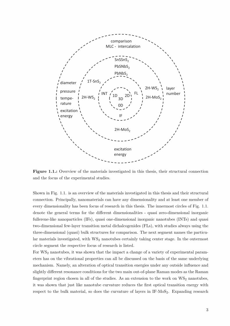
Figure 1.1.: Overview of the materials investigated in this thesis, their structural connectionand the focus of the experimental studies.
Shown in Fig. 1.1. is an overview of the materials investigated in this thesis and their structuralconnection. Principally, nanomaterials can have any dimensionality and at least one member ofevery dimensionality has been focus of research in this thesis. The innermost circles of Fig. 1.1.denote the general terms for the different dimensionalities - quasi zero-dimensional inorganicfullerene-like nanoparticles (IFs), quasi one-dimensional inorganic nanotubes (INTs) and quasitwo-dimensional few-layer transition metal dichalcogenides (FLs), with studies always using thethree-dimensional (quasi) bulk structures for comparison. The next segment names the particu-lar materials investigated, with WS2 nanotubes certainly taking center stage. In the outermostcircle segment the respective focus of research is listed.For WS2 nanotubes, it was shown that the impact a change of a variety of experimental param-eters has on the vibrational properties can all be discussed on the basis of the same underlyingmechanism. Namely, an alteration of optical transition energies under any outside influence andslightly different resonance conditions for the two main out-of-plane Raman modes as the Ramanfingerprint region chosen in all of the studies. As an extension to the work on WS2 nanotubes,it was shown that just like nanotube curvature reduces the first optical transition energy withrespect to the bulk material, so does the curvature of layers in IF-MoS2. Expanding research
3

into the field of planar layered structures, where dimensionality has been found to determinewhether WS2 and MoS2 are indirect or direct band gap semiconductors, and being aware of thespecific information Resonance Raman spectra have to offer, the out-of-plane modes were onceagain in the focus of attention during work on FL-WS2. Here, and in FL-MoS2 as well, Ramanspectra were found to contain information about the characteristics of the excitons the phononscouple to in the resonant case.There are two main polytypes in layered (transition) metal dichalcogenides (TMDs), commonlydenoted by the prefix 2H and 1T , and pristine INTs, 2H-WS2 and 1T -SnS2 NTs, respectively,of both types have been investigated in this thesis. For the later work on misfit layer com-pounds (MLCs) this was of advantage, as their Raman spectra can be discussed on the basis ofthe Raman spectra of their constituents. Raman spectroscopy on both 2H-derived NbS2 and1T -derived SnS2 MLC nanotubes, was carried out in the course of the present thesis with thescientific focus on the comparison with the respective parent bulk structures on the one handand NbS2 nanotubes intercalated with lead atoms on the other hand. Misfit layer nanotubesrepresent an interesting mix of different dimensionalities with their alternate stacking of quasitwo-dimensional TS2 and MS layers and their rolling-up to large diameter nanotubes that closelyresemble the three-dimensional bulk misfit structures. Interlayer interaction as a basic factorstabilizing all of the layered inorganic materials has influence on the vibrational characteristicsin the pristine compounds, for instance in different layer number FL-WS2, despite being of weakvan der Waals character. In misfit layer compounds interlayer interaction determines the vibra-tional frequencies in an unprecedented way and models explaining the remarkable changes inRaman frequencies have to go well beyond the simple van der Waals bonding.The outline of this thesis is as follows. I will first introduce the basic structural properties ofthe inorganic layered materials, their combination in misfit layer compounds and the specificsof their appearance as nanotubes in Chapter 2. Then, I will concentrate on the electronic prop-erties of above named compounds in Chapter 3. Knowledge of both, structural and electroniccharacteristics and their interplay were of vital importance for the papers forming this thesisthat are listed in Chapter 4. Their connection and scientific output is discussed in Chapter 5with the focus on the vibrational properties as the main topic of my work on low-dimensionalinorganic layered materials. An outlook summarizing the results and presenting perspectives offuture work on these kind of nanostructures concludes this thesis in Chapter 6.
4

2.1. Structure of layered materials
Structural properties2
2.1. Structure of layered materials
The TS2 layers
The structure of a layered compound is defined by the coordination of atoms within a layerand by how these layers as a whole are arranged with respect to each other. The formula TX2
comprises compounds where in each trilayer the (transition) metal atom T is coordinated bythree chalcogen X atoms above and below that form the base of two tetrahedrons with the T
atom in the middle layer as the tip. Because almost all research is performed on compoundscontaining sulfur, in this thesis I will mostly speak of TS2 compounds. In the trigonal prismaticcoordination the tetrahedrons have the sulfur atoms within one layer on top of each other, whilein the octahedral coordination they are rotated by 60° with respect to each other. The corre-sponding structural abbreviations are AbA and AbC (where A and C denote sulfur layers andb the metal atoms) [1], respectively, and both types are shown in Fig. 2.1. Typical examplesof trigonal prismatic arrangement (H type) within a metal dichalcogenide layer are MoS2, WS2
and NbS2, whereas e.g. TiS2 and SnS2 layers crystallize in the octahedral coordination (T type).The octahedrally coordinated layers commonly obey the simplest possible stacking order: theunit cell of 1T -TS2 is only one layer thick and individual layers are placed exactly on top of eachother (AbC AbC) [Fig 2.1.(a)]. In contrast, the hexagonal 2H trigonal prismatic stacking orderhas its unit cell spanning over two layers [Fig 2.1.(b)]. Consequently, in the rhombohedral 3R
stacking the sequence of layers is repeated only every three layers. The 2H structure has twosub-polytypes that are important to discuss here. In the 2Ha structure (e.g. NbS2) the metalatoms are found on top of each other, but the tetrahedrons from neighboring layers are rotatedby 60° (AcA BcB). The 2Hb structure (e.g. WS2) has an additional in-plane shift of layers,meaning that metal atoms are found above and below sulfur atoms of adjacent layers. Again,this is illustrated in Fig. 2.1.(b). There is only one 3R polytype (AbA BcB CaC) for bothWS2 and NbS2. Without going further into detail concerning the symmetry of the investigatedmaterials, in the Schönfliess notation the space groups of the 1T compounds are D3
3d for thebulk and an unchanged point group symmetry D3d in the individual layers, the 2H materialspossess D4
6h symmetry in the bulk and D3h in the monolayer.
5

trigonal prismaticoctahedral
2Ha-NbS2
A
c
A
c
B
B
P63/mmc46hD1T-SnS2
A
b
C
A
b
C
P m1333dD 2Hb-WS2 P63/mmc
A
b
A
A
b
b
46hD
(a) (b)
cba c
bac
ba
Figure 2.1.: Basic structures of transition metal dichalcogenides. (a) Structure of TMDs inoctahedral coordination (1T ); the unit cell is one triple layer thick. (b) The two types of TMDsin trigonal prismatic coordination (2H) with the unit cell spanning over two triple layers. Thespace groups of the bulk structures are denoted below the compounds, the stacking arrangementsare found in italic letters on the right side of the TMDs.
As a consequence of rather weak interlayer interaction, there is the occasional problem of nonsto-ichiometry particularly for 3R-NbS2 [2, 3], with additional Nb atoms found in the van der Waalsgap. More importantly, however, intercalation of metal dichalcogenides with atoms, organicmolecules or other types of layered materials is widespread.
The MS layers
One class of materials that can be found as guest layers in between host TS2 layers are cubicmonochalcogenides. The general formula MX with M a metal or a rare earth element andX a chalcogenide describes a two atom thick layer cut out from the (001) plane of a (hypo-thetical) three-dimensional NaCl-type structure. Lead monosulfide is one example of such anintercalant. PbS (Galena) occurs in nature as a three-dimensional crystal with NaCl structure.Its appearance as a MS double layer (half the thickness of a NaCl unit cell) is only reportedas an intercalant of TX2 transition metal dichalcogenides and results in strong distortion com-pared to the bulk structure. Recent HRTEM (high resolution transmission electron microscopy)investigations [4] are able to show, down to a few picometres, how the lead atoms of PbS inthe misfit layer compound are always closer to the neighboring TS2 layer than its sulfur atoms.Tin sulfide, as another example, has in its pristine form a layered α-phase with GeS structureand an orthorhombic (pseudo-tetragonal highly distorted NaCl) unit cell [5, 6]. In misfit layercompounds (MLCs), however, it is found to adopt a structure similar to the lead sulfide part inPbS-based MLCs [7, 8].
6

2.2. The misfit layer compounds
c
b
aNbS2
a*PbS(a)
aNbS2
a*PbS
b/b*
CC
c
b CF
c
bCC
c
b
(b)
(c)
(d) (e)
chalcogenide
transition metal
metal
c
Figure 2.2.: Basic structure of MLC (adapted from Refs. [9, 10]). (a) Sketch of the basicalternate stacking of MX and TX2 layers in (PbS)1.14NbS2 along a common c direction with acommensurate b and incommensurate a lattice constants. (b) Simple CC stacking sequence forTMDs in trigonal prismatic (left) and octahedral (right) coordination. (c) CF stacking sequenceadopted for example by the (PbS)1.14NbS2 compound, seen along the stacking c direction. Thesulfur atoms of the PbS part are omitted for clarity. (d) The CF stacking sequence seen along theincommensurate a direction.(e) Basic structure of the intercalation compound PbNbS2. Viewalong the normal to the (11.0) plane according to the pseudohexagonal system of labeling ofthe NbS2 material intercalated with lead atoms in linear coordination to neighboring S atoms(ICSD col. code. 74698). Panels (b)-(e): different colors of the same element represent atomicpositions half a lattice constant apart, the black lines refer to the size of the unit cell.
2.2. The misfit layer compounds
When the two subsystems described above, the TS2 trilayers and the MS double layers, arecombined, the structure that follows is commonly termed a misfit layer compound (MLC).(PbS)1.14NbS2 and the SnS-SnS2 system are two MLCs that have been studied in the course ofthis thesis. Exemplary MLC structures are shown in Fig. 2.2. Some of the structural parametersdiscussed below are presented in Table 1. In these compounds, the TS2 and MS layers share
7
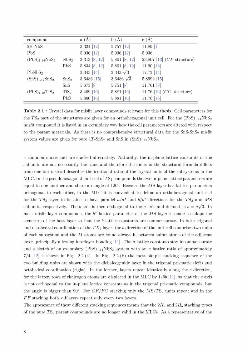
compound a (Å) b (Å) c (Å)2H-NbS 3.324 [12] 5.757 [12] 11.89 [1]PbS 5.936 [12] 5.936 [12] 5.936(PbS)1.14NbS2 NbS2 3.313 [8, 12] 5.801 [8, 12] 23.807 [13] (CF structure)
PbS 5.834 [8, 12] 5.801 [8, 12] 11.90 [13]PbNbS2 3.343 [14] 3.343
√3 17.73 [14]
(SnS)1.17SnS2 SnS2 3.6486 [15] 3.6486√
3 5.8992 [15]SnS 5.673 [8] 5.751 [8] 11.761 [8]
(PbS)1.18TiS2 TiS2 3.409 [16] 5.881 [16] 11.76 [16] (CC structure)PbS 5.800 [16] 5.881 [16] 11.76 [16]
Table 2.1.: Crystal data for misfit layer compounds relevant for this thesis. Cell parameters forthe TS2 part of the structures are given for an orthohexagonal unit cell. For the (PbS)1.14NbS2
misfit compound it is listed in an exemplary way how the cell parameters are altered with respectto the parent materials. As there is no comprehensive structural data for the SnS-SnS2 misfitsystem values are given for pure 1T -SnS2 and SnS in (SnS)1.17NbS2.
a common c axis and are stacked alternately. Naturally, the in-plane lattice constants of thesubunits are not necessarily the same and therefore the index in the structural formula differsfrom one but instead describes the irrational ratio of the crystal units of the subsystems in theMLC. In the pseudohexagonal unit cell of TS2 compounds the two in-plane lattice parameters areequal to one another and share an angle of 120°. Because the MS layer has lattice parametersorthogonal to each other, in the MLC it is convenient to define an orthohexagonal unit cellfor the TS2 layer to be able to have parallel a/a* and b/b* directions for the TS2 and MSsubunits, respectively. The b axis is then orthogonal to the a axis and defined as b = a
√3. In
most misfit layer compounds, the b* lattice parameter of the MS layer is made to adopt thestructure of the host layer so that the b lattice constants are commensurate. In both trigonaland octahedral coordination of the TX2 layer, the b direction of the unit cell comprises two unitsof each subsystem and the M atoms are found always in between sulfur atoms of the adjacentlayer, principally allowing interlayer bonding [11]. The a lattice constants stay incommensurateand a sketch of an exemplary (PbS)1.14NbS2 system with an a lattice ratio of approximately7/4 [12] is shown in Fig. 2.2.(a). In Fig. 2.2.(b) the most simple stacking sequence of thetwo building units are shown with the dichalcogenide layer in the trigonal prismatic (left) andoctahedral coordination (right). In the former, layers repeat identically along the c direction,for the latter, rows of chalcogen atoms are displaced in the MLC by 1/6b [11], so that the c axisis not orthogonal to the in-plane lattice constants as in the trigonal prismatic compounds, butthe angle is bigger than 90°. For CF/FC stacking only the MS/TS2 units repeat and in theFF stacking both sublayers repeat only every two layers.The appearance of these different stacking sequences means that the 2Ha and 2Hb stacking typesof the pure TS2 parent compounds are no longer valid in the MLCs. As a representative of the
8

2.3. Structure of inorganic nanotubes
CF stacking sequence, the structure of bulk (PbS)1.14NbS2 is depicted in a top-view on the ab-plane in Fig. 2.2.(c) and along the incommensurate a direction in Fig. 2.2.(d). The mismatchof the two materials is expressed in the general structure formula of misfit layer compounds(MX)1+δ(TX2)n as the parameter 1+δ with δ = 1 − a
a*/2 [17]. This takes into account that thea* lattice constant of the MX material spans across two formula units. The two extreme casesfor the parameter δ are represented by (YS)1.28CrS2 [18] and (BiS)1.08TaS2 [19]. The additionalparameter n denotes the number of TX2 slabs in between MX slabs and takes values betweenn = 1 (stage 1 MLC [20]) and n = 3 (stage 3 MLC). The influence that the two materialsexert on each other when combined to a misfit layer compound has been widely discussed withdrastically differing results (see Chapter 3). Structurally, though, it is evident from a numberof experiments that the TX2 layer remains fairly rigid [8], while the MX layer exhibits strongdistortion beyond the fact that it is in a very unusual two-dimensional configuration with everyatom being a surface atom [4]. Not only has the b* lattice constant to adopt the b latticeconstant of the TX2 slab, it is also observed that the M atoms always protrude into the van derWaals gap [4], probably owing to the presence of a lone pair of electrons.Even though it is not a misfit layer compound but a true intercalation compound, the unusualstructure of PbNbS2 shall be mentioned here. In most cases, atoms intercalated in transitionmetal dichalcogenides will fill the interstices of the sulfur atoms resulting in structures likePb1/3TX2 [14]. In PbNbS2 however, lead atoms are linearly coordinated by neighboring sulfuratoms, see Fig. 2.2.(e) [14].
2.3. Structure of inorganic nanotubes
Pristine inorganic nanotubes
A report on inorganic nanotubes never misses to reference carbon nanotubes (CNTs) as the ma-terial whose discovery in 1991 [21] laid the foundation of an entirely new research area. Shortlyafter, in 1992, Reshef Tenne and coworkers [22] synthesized tubular structures of WS2 as thefirst member of the ever since growing family of inorganic nanotubes. The following paragraphswill concentrate on WS2 and SnS2 nanotubes in particular, a comprehensive list of inorganicnanotubes that have been synthesized during the last two decades can be found in Ref. [23].Being an inorganic analogue to carbon nanotubes, WS2 nanotubes are hollow cylindrical struc-tures with a large length to diameter ratio, made of several rolled-up S-W-S triple layers. In fact,it can be shown that, above a critical diameter threshold, the annihilation of dangling bondson the rim of multilayer WS2 stripes by spontaneous bending is energetically preferred to thestrain energy associated with the bending of the nanotube walls [24]. Obviously, there is a higherstrain energy involved in the bending of a WS2 layer than in graphene sheets that form the basisfor the formation of carbon nanotubes. Consequently, in contrast to CNTs, the diameters ofWS2 nanotubes are never in the subnanometer regime, but cover a wide diameter range startingwith a lower limit of the inner diameter of around 4 nm [22]. The always multiwalled form of
9

WS2 and other inorganic nanotubes appears to be another stabilization criterion. IndividualWS2 nanotubes with less than 4 walls have not been observed so far [24], typically the numberof walls amounts to 10-50, outer diameters range from 7 to 290 nm and lengths are hundredsof nanometer to several micrometers [22, 24–27]. Structurally, a lot depends on the synthesismethod and growth conditions and, using techniques such as transmission electron microscopy(TEM), high resolution TEM (HRTEM), X-ray diffractometry (XRD), electron diffraction (ED)and theoretical modeling, a plethora of different subtypes has been revealed on the atomic level.For example, Remškar et al. [28–31] report on nanotubes that are formed by the continuous spi-ral winding of one single molecular WS2 layer around the tube axis and can be more accuratelydescribed as nanoscrolls. Others find nanotubes where the shells grow separately, possibly usingone original shell as a growth template [32, 33], in a coaxial, russian doll-like fashion. Whereasnanotubes with diameters up to 30 nm have been shown to possess a near perfect cylindricalcross section [25, 34], thicker nanotubes adopt a polygonal cross section [31, 34] that is pre-dicted to be energetically more favorable [35]. The nanotubes are either open-ended [31] orhave closed caps that exhibit a large number of possible angles with most of them identicalwith angles occurring in regular polygons [36]. Almost round caps are seen predominantly insmall diameter nanotubes [22] while 90° angles have been observed in thicker WS2 nanotubes[34]. The tube diameter also plays a role in determining the stacking order of subsequent WS2
walls. The stacking can be investigated by either ED patterns [36] or HRTEM on the atomiclevel [37]. There are reports that conclude that the hexagonal 2Hb stacking type predominatesfor nanotube diameters up to 200 nm while for larger microtubes the rhombohedral 3R stackingtype has been identified [29]. However, as Ref. [37] rightly points out, statements on a specificbulk derived stacking order have to be taken with caution and a more or less random stackingorder seems to be more likely. To begin with, with each shell the tube circumference is enlargedby 2πc0, where c0 = c/2 is half the c lattice constant perpendicular to the tube axis (the factortwo is included because, in the bulk structure, the unit cell stretches out over two triple layers).In order to satisfy a strict bulk pattern, this parameter would need to be an integer multipleof the in-plane lattice parameter in winding direction [30]. In comparison with the c/2 latticeparameter of the pristine WS2 crystal (0.6181 nm [1]) the wall thickness is seen to be slightlyexpanded in the WS2 nanotubes [36, 38, 39] and is not a multiple of the in-plane lattice con-stant a of 0.3154 nm [1]. Secondly, contradicting evidence is also presented concerning a centralquestion that also influences the lattice matching of adjacent layers: the chirality of the tubewalls. Similar to carbon nanotubes the direction of the rolling-up of molecular layers can becharacterized by a chirality vector �c = n1�a1 + n2�a2, with the two in-plane basis vectors �a1 and�a2 sharing an angle of 60° and the two chiral indices (n1,n2) having to be integer numbers. Dueto their respective appearance on the rim (n1,0) nanotube walls are called zigzag with a chiralangle of 0° and (n1,n2 = n1) nanotubes are called armchair, while every other pair of chiralindices characterizes chiral nanotube walls. Considering the spiral winding growth mode onecan assume that there is either only one chiral angle present in these nanotubes or, under theinfluence of internal strain, several with very similar chiral angles [30]. In the coaxial-cylindrical
10

2.3. Structure of inorganic nanotubes
growth mode, apart from one report that observed achiral armchair walls [32], the majority ofauthors find nanotubes with small chiral angles towards the zigzag character and a deviationof only a few degrees from one wall to another or pure zigzag walls [27, 32, 33, 36, 38, 40]. Itcan generally be stated that, despite the fact that there is considerable strain involved in thebending of the nanotube walls, with the inner sulfur layer experiencing compressive and theouter sulfur layer tensile stress with respect to the tungsten layer in the middle, WS2 nanotubespossess a remarkable degree of structural uniformity with most of the walls appearing almostdefect free.While the layers in WS2 nanotubes are in trigonal prismatic coordination, the SnS2 nanotubesinvestigated in this thesis are an example of inorganic nanotubes with layers in the octahedralcoordination. Although short, tubular-like SnS2 structures [41] and small amounts of SnS2 nan-otubes [42, 43] have been synthesized before, a detailed analysis of 1T -SnS2 nanotubes was firstpresented by Radovsky et al. [5]. The nanotubes are straight and TEM images show evenlyspaced fringes with an interlayer distance of 0.59 nm, corresponding to the c lattice parameterof bulk 1T -SnS2 (Berndtite) [44]. From the splitting of reflection spots in the measured diffrac-tion patterns the almost monohelical nature of the walls of an exemplary SnS2 nanotube and asmall chiral angle of around 4° was derived [5]. Even the nanotubes characterized as pure SnS2
include some layers of SnS mostly close to the hollow core of the nanotube that form an orderedSnS-SnS2 superstructure. The vast majority of nanotubes containing tin can be characterizedas misfit layer nanotubes with a variety of ordered stacking sequences of SnS and SnS2 slabs.This SnS-SnS2 system as well as the PbS-NbS2 system also investigated in this thesis shall beexamined in more detail in the next section.
Misfit layer inorganic nanotubes
Misfit structures have been known to form fullerene-like and tubular morphologies on thenanometer scale for quite some time and in recent years a number of compounds have beenadded to a now extensive list of inorganic misfit layer nanotubes [45]. It was mentioned beforethat for pure inorganic nanotubes the main driving force for bending is the energetic advan-tages of a healing of dangling bonds on the periphery of the planar layers. Here, in misfit layercompound nanotubes, the intrinsic stress associated with the mismatch of neighboring layershas been established as an additional mechanism that promotes the rolling-up of layers [5, 12].It is assumed that the relaxation of misfit stress by folding of layers occurs predominantly forasymmetric lamellae, that is, if top and bottom layer are of different material [12]. Naturally,the favored rolling vector will be in the direction the lattice constants of the subsystems differthe most, the incommensurate a direction. Thus, the tube axis is expected to coincide with thecommensurate b direction (for a definition of the lattice axes, see previous section) [7]. However,as we will see, the individual layers do not always obey these rules and they can merely be seenas a general trend. Compared to pristine inorganic nanotubes the diameters of misfit layer NTsare larger in average, most probably due to the higher rigidity of their chemical bonds resulting
11

(a)
(b)
(c)
(d)
(e)
(f)
Figure 2.3.: Structural characterization methods of (PbS)1.14NbS2 and PbNbS2 nanotubes.Descriptions in the text. Adapted from Fig. 5 and Fig. 7 of Ref. [6].
in higher folding energies. Both, nanoscrolls and nanotubes with concentric individual wallsare encountered with the ratio nanoscrolls vs. nanotubes depending on the growth conditionsand, more importantly, on the symmetry of the crystals. High symmetry favors the formationof nanotubes as the facets are more easily seamed [45]. A variety of growth steps leading to atelescope-like shape of the nanotube as a whole, particularly in larger diameter misfit layer nano-scrolls [7], conical tubules as well as nanoscrolls with partly unfolded sheets have been observedquite frequently [6, 7, 45, 46]. Contributing to the wealth of appearances are dislocation-like de-fects that could possibly lead to a transition from nanoscrolls to nanotubes by an “unzippering”mechanism [6] and thin nanotubes with constant outer diameters of 20-40 nm that could serveas template for further scrolling of additional misfit sheets [7].Shown in Fig. 2.3. are different steps of the structural analysis of an exemplary (PbS)1.14NbS2
nanotube. The misfit layer nanotube pictured in Fig. 2.3.(a) exhibits alternating layers of PbSand trigonal prismatically coordinated NbS2, stacked along a common c axis. A line profile ofthe region enclosed in the rectangle in panel (a) [Fig. 2.3.(e)] as well as a scanning transmissionelectron microscope high-angle annular dark-field (STEM-HAADF) image (of another similarnanotube) [Fig. 2.3.(c)] reveals equidistant fringes of 1.20 nm that correspond to half the c lat-
12

2.3. Structure of inorganic nanotubes
tice parameter of 2H-NbS2 plus the c lattice parameter of a PbS layer. A lot about the innerstructure of the nanotube can be learned from the selected area electron diffraction (SAED)patterns of panel (b). Without going too much into detail, the periodicity along the c axis canbe confirmed, interplanar spacings and Miller indices can be derived from the sets of reflectionpoints equi-azimuthally distributed on circles (red for NbS2, green for PbS) and the splittingof these sets of reflection points allows for the deduction of a small chiral angle of 5.5° (halfof the 11° splitting). In the ortho-hexagonal unit cell of NbS2 (with orthogonal lattice axes,see previous section) there are three possible and equivalent orientations rotated by 60° for theadjacent PbS layer, the presence all of which can be identified in the diffraction pattern of panel(b). Schematically, the different orientations of the PbS layer with respect to the NbS2 layer areshown in the inset of panel (c) - only one of them has its b axis in the direction of the nanotubeaxis - but in the nanotube all of them share the same chiral angle, that is, 5.5° in this case.Actually, most (PbS)1.14NbS2 nanotubes were found to possess a (small) chiral angle [6, 45].Even though in the b direction the PbS layer adopts to the NbS2 b-parameter, a small mismatchmay be accommodated by a small deviation from this “commensurate” direction [6, 12]. As inthe bulk misfit structure, both, stage 1 [6] and stage 2 [12] nanotubes seem to exist.NbS2 nanotubes intercalated with lead atoms and a c-periodicity of 0.88 nm were also observed[6] and a STEM-HAADF picture as well as a line profile of a PbNbS2 nanotube are depictedin Fig. 2.3.(d) and (f), respectively. The lead atoms are linearly coordinated to adjacent sulfuratoms (Fig. 2.3.(d) inset), Pb and NbS2 layers alternate, and the ratio between the niobium andlead atoms is close to 1:1. These PbNbS2 nanotubes have uniform inner and outer diameter,are sometimes more than 10 μm long and are believed to grow unidirectionally [6]. The outerdiameters of (PbS)1.14NbS2 and PbNbS2 nanotubes range typically between 50 and 250 nm butcan reach diameters up to 500 nm.Nanotubes comprising SnS and SnS2 investigated in this thesis are the prototype for misfitlayer NTs with octahedral coordination of TS2 layers. Reference [7] presents the synthesis andcharacterization of (SnS)1.32SnS2, (SnS)1.32(SnS2)2 and [(SnS)1.32]2[SnS2]3 nanotubes. Whilecharacterization methods and basic structural concepts such as predominant small chiral anglesresemble the above description of Pb-Nb-S nanotubes, the coexistence of different polytypes re-flects the stronger autonomy of individual layers and weaker interlayer interaction. SnS and SnS2
layers do not always alternate along their common c axis, but form ordered superstructures ofthe sequence O-T-T, O-T and O-T-O-T-T (in order of abundance, O stands for the orthorhom-bic SnS, T for the SnS2 lattice) with evenly spaced fringes seen in the line profiles of 1.74 nm(0.56+0.59+0.59 nm), 1.15 nm (0.56+0.59 nm) and 2.89 nm (0.56+0.59+0.56+0.59+0.59 nm),respectively [6]. Random stacking is rarely encountered [7]. The interplanar spacings of bothsubsystems remain practically unaltered relative to their respective parent compounds, henceboth in-plane lattice parameters are principally incommensurate in the SnS-SnS2 system, incontrast to the Pb-Nb-S system [6, 7]. Not only is this further evidence of weak interlayerinteraction but also of a higher degree of freedom regarding interlayer orientation which leadsto multiple helicities and in-plane orientation of neighboring layers. However, there is still a
13

preferred orientation with specific planes of SnS and SnS2 roughly coinciding with the tube axis.Typical diameters of SnS-SnS2 nanotubes are 20-60 nm for straight tubules and up to 160 nmfor nanotubes with growing steps. The diameters are thus smaller than those observed in thePb-Nb-S system, probably due to higher rigidity of bonds in Pb-Nb-S materials [6].
14

3.1. Transition metal dichalcogenides
Electronic properties3
3.1. Transition metal dichalcogenides
The structure of the (transition) metal dichalcogenides discussed in detail in the last chapterdetermines the electronic properties of this family of materials. Metal cations of group IVA (Sn),IVB (Ti, Zr, Hf), VB (V, Nb, Ta) and VIB (Cr, Mo, W) are surrounded by six chalcogen anions(S, Se, Te) in sandwich-like trilayers that are stacked upon each other. Bonding within the layersis of covalent or ionic nature and contrasts the weak interlayer forces of van der Waals charac-ter. Owing to the layered structure, many of the electrical and optical properties are extremelyanisotropic. Consequently, the term quasi two-dimensional materials is frequently used. Recentyears have seen a tremendous increase in interest in layered TMDs that - in analogy to a famousarticle about graphene [47], the mother of two-dimensional materials - could be called “the riseof transition metal dichalcogenides”. One of the advantages over graphene is the diversity ofelectronic properties and, most importantly, a sizable band gap in materials like MoS2. Whilethe renewed interest in TMDs is due to the exploration of their properties as low-dimensionalmaterials (few-layer, see section 3.3, and nanotubes, see section 3.4) the bulk materials are wellknown and their properties have been investigated for decades. A comprehensive review waspublished already in 1969 by Wilson and Yoffe [1] and includes transmission spectra as well as asimple electronic structure model derived from the ligand-field theory. It is best explained withthe help of Fig. 3.1. In the TX2 materials, the chalcogen s and p orbitals form the occupiedbonding and unoccupied antibonding σ and σ* bands below and above the Fermi energy. Tobe fully occupied and adopt the energetically attractive noble gas configuration, each of the twochalcogen valence band ns2np4 orbitals needs two electrons. These are supplied by metal s andd electrons, leaving them in the oxidation T 4+ status while the chalcogen atoms reach the X2−
oxidation status. Thus, there are now a total of 16 electrons (4 s and 12 p electrons) in thevalence band. In the energy gap between the chalcogen valence orbitals and the unoccupiedchalcogen conduction band states, the d orbitals of the metal atoms are situated. For the oc-tahedral compounds, they are energetically split into a twofold degenerate eg level, composedof dz2 and dx2−y2 orbitals and a threefold degenerate t2g level with dyz, dxz, dxy orbitals. Fortrigonal prismatic compounds, the d states split into three groups, dz2 (a1), dx2−y2 , dxy (e),
15

NbS2 WS2TiS2
DOS DOS DOS
E d0 d1 d2
octahedral trigonal prismatic
s (4)
p/d (12)
σ
σ*E
EFEF
E
EF
dz2,x2-y2 (4)
dyz,xz,xy /p (6)
s,p
eg
t2g
dz2 (2)dxy,x2-y2 (4)
dxz,yz /p (4)
s (4)
p/d (12)
σ
σ* s,p
e‘ea1
(a) (b)
Figure 3.1.: Adapted from Ref. [48] (octahedral compounds) and Ref. [49] (trigonal prismaticcompounds). This simple electronic band scheme was first introduced by Wilson and Yoffe[1] and depicts the successive filling of the dz2 band determining the electronic properties ofoctahedrally coordinated group IVB transition metal dichalcogenides to trigonal prismaticallycoordinated group VB and VIB TMDs.
and dxz, dyz (e′), and between the first two there is an energy gap of around 1 eV [48]. Theirelectron population - and for the group IVB, VB and VIB TMDs more specifically the degreeof filling of the narrow dz2 band - determines the electronic properties of the transition metaldichalcogenides. The type of chalcogen atom, sulfur, selenium or tellurium has little influenceon the electronic structure of the TMDs.Starting with TiS2 as a representative of the group IVB TMDs, as a consequence of the titanium3d24s2 valence electrons being transferred to the sulfur orbitals, above the Fermi energy, the TiS2
dz2 orbital is empty, as shown in Fig. 3.1.(a). Most of the group IVB TMDs are consequentlysemiconductors or in some cases semimetals due to d-p orbital overlap [1, 49, 50]. Similarly tothe IVB materials, the SnS2 group IVA metal dichalcogenide is a semiconductor with the tin5s25p2 valence orbitals emptied by electron transfer to the sulfur atoms. A reported indirectband gap energy of SnS2 is 2.06 eV [51]. SnS2 as well as all of the IVB TMDs crystallize in theoctahedral 1T bulk structure (see Chapter 2).NbS2 is the representative of the group VB transition metal dichalcogenides investigated in thisthesis. The depopulation of the niobium 4d45s1 valence orbitals leaves all but one d1 electronin the NbS2 dz2 orbital. The Fermi energy crosses this half-filled orbital in the middle and allof the VB TMDs are therefore of metallic character [see Fig. 3.1.(b)]. In Fig. 3.2. a calculatedband structure of bulk NbS2 [52] along the high symmetry lines of the Brillouin zone basicallyconfirms the simple picture developed by Wilson and Yoffe. It also shows that for the case ofNbS2 there is no so-called p-d gap between the dz2 band and lower lying p orbitals, as the latter
16

3.1. Transition metal dichalcogenides
A
M
HL
Kky
kz
kx
Γ
NbS2 WS2
0.2
0
-0.2
E F[Hartree]
M K KMΓΓΓ Γ
Figure 3.2.: Shown are the electronic band structure (calculated in and adapted from Ref.[52]) for the metal group VB TMD NbS2 with bands crossing the Fermi energy at several pointswithin the Brillouin zone and for the semiconducting group VIB TMD WS2, where excitons atthe K-point (not shown here) play an important role in determining the electronic properties.Shown on the right side is the Brillouin zone of the hexagonal lattices.
are seen crossing the Fermi level around the Γ-point.In contrast to the group IV compounds, there are 2H (NbS2) as well as 1T polytypes presentwith TaS2 found in both configurations. An important feature of group VB TMDs is, with fewexceptions including 2H-NbS2 [53], the development of a PLD-CDW (Peierls lattice distortion- charge density wave) below a critical temperature T0 [49]. This phenomenon is only present inquasi one- and two-dimensional materials and describes the occurrence of a periodic modulationof the electron density together with a distortion of the ions forming the periodic lattice. Thelatter creates a new super unit cell accompanied by an energy gain that compensates, below T0,for the energy spent for the electron and ion distortion. In quasi one-dimensional materials, theelectron energy reduction at the Fermi energy leads to a metal-insulator transition, however,this is not necessarily the case for the layered TMDs which stay metallic [49]. Typical onsettemperatures are around 600 K for compounds in the octahedral and below 100 K for compoundsin the trigonal prismatic arrangement [49]. At even lower temperatures the group VB TMDsexhibit superconductivity in the single digit range, a recent value for Tc in NbS2 for example is6.05 K [54].The group VIB transition metal dichalcogenides containing molybdenum and tungsten are semi-conductors due to their dz2 orbital being fully occupied with two electrons [see Fig. 3.1.(b)].There is pronounced hybridization between sulfur p orbitals and metal d orbitals [55]. Chromium-based materials as a third member of the group VIB TMDs are unstable in layered form andonly exist as part of misfit layer compounds. Structurally, for the VIB TMDs, MoS2 and WS2
crystallize in the trigonal prismatic coordination, whereas the chromium atom is octahedrallycoordinated to six sulfur atoms in chromium-based MLCs [56]. The indirect band gap of molyb-
17

denum and tungsten compounds is in the near infrared [57]. Concentrating on WS2 as thematerial investigated in this thesis, experimental values for the indirect band gap range between1.35 and 1.4 eV [58–60], with the top of the valence band situated at the Γ-point while the lowestconduction band state is halfway between Γ- and K-point [52, 61, 62], see Fig. 3.2.
Figure 3.3.: WS2 single crystal absorptionspectrum in the vicinity of the band gap withprominent A and B exciton peaks [63].
The lowest direct band gap on the other handis found at the K-point and the optical transi-tions of the group VIB TMDs are governed byexcitons, which in contrast to the group VBTMDs are not screened out by free carriers.Absorption measurements reveal the presenceof a number of peaks, typically labeled A andB for the most pronounced exciton features atthe absorption edge and a broader band C athigher energies. Exemplary, this is shown forWS2 in Fig. 3.3. [63] and values for the A
and B exciton reported are 1.95 and 2.36 eV,respectively [58]. They arise as a result of ver-tical optical transitions from a spin-orbit splitvalence band at the K-point to the conduc-tion band [62]. The presence of excitons com-plicates the determination of the size of thedirect band gap. Assuming an exciton bind-ing energy of 0.06 eV, Ballif et al. [58] estimatea value of 2.01 eV at room temperature. A calculated band structure of WS2 along the Γ-K-M -direction is depicted in Fig. 3.2. for the middle plane of the hexagonal Brillouin zone shownon the right. In the upper plane along the A-H-L-A high symmetry points, the band structurelooks similar, but the bands that are split in the Γ-K-M -plane are double degenerate in theupper plane [55, 61].
3.2. Misfit layer compounds
Research on the electronic structure of misfit layer compounds MX/RX−TS2 (M = Pb, Sn;R = rare earth metal, T = Ti, Nb, Ta, Cr...; X = S, Se, Te) is basically driven by a singlequestion: how and to what extent do the two subsystems influence each other and how is theremarkable stability of misfit compounds to be explained? The alternately stacked constituentsin the MLC are neither electronically nor geometrically similar, yet, they form ordered super-structures that can be chemically synthesized [41, 64, 65]. Layered chromium disulfide even onlyexists by virtue of the interaction with the monochalcogenide layers in the misfit compound LaS-
18

3.2. Misfit layer compounds
CrS2 [11, 45, 66]. It can be generally stated that the formation of misfit layered compounds isrestricted to divalent metals M , like Sn2+ and Pb2+ with a lone pair of electrons or trivalent rareearth metals R like La3+ or Ce3+ [67]. Historically, before research on misfit layer compoundsgained momentum, the intercalation of TMDs with alkali metals and other electron donors wasthoroughly investigated [49]. It was generally found that an electron transfer from the interca-lated atoms to the TX2 layers takes place and, to continue with the above mentioned example,is the raison d’être for layered CrS2 [68]. The electron donation results in an increased ionic-ity and therefore a stronger bonding between the layers. The main concepts of the electronicstructure of TS2 intercalation compounds were then later adopted for misfit layered compoundsin that a charge transfer was assumed to play a stabilizing role. Because interlayer interactionis weaker than the covalent intralayer bonds, the MS layers are often regarded as intercalationderivatives of layered transition metal dichalcogenides. From an electronic structure point ofview, considering the MS and the TS2 layer as two separate constituents has the consequencethat the band structure of the misfit layered compound may be constructed by a superpositionof the band structures of the subsystems.This rigid band model has found widespread application in trying to explain the band structuresof MLCs. Many authors state that it is a good first approximation with the only change beinga charge transfer from the MS layer to the TS2 layer and a subsequent adjustment of the Fermilevel. The concept is shown schematically in Fig. 3.4. for the misfit compounds (PbS)1.18TiS2
(a) and (PbS)1.14NbS2 (b). In the octahedrally coordinated group IVB TiS2 compound the broad3d conduction band is either completely empty or only slightly filled, depending on whether it isconsidered a semiconductor or a semimetal in the pristine compound (see previous section), and
S 3p
PbS TiS2(PbS)1.18TiS2 PbS (PbS)1.14NbS2 NbS2 (PbS)1.14NbS2
Pb 6s
S 3s S 3s
S 3p
Ti 3dS 3p
Pb 6s
S 3s
NbS2dz
2
S 3p
S 3s
p/d gap
DOS DOS DOS
E EE(a) (b) (c)
Figure 3.4.: Concept of the rigid band model illustrated for an octahedrally coordinated groupIVB (a) and a trigonal prismatically coordinated group VB misfit layer compound (b): the elec-tronic band structure can be seen, to a first approximation, as a superposition of the electronicstructure of the subsystems. (c) Phenomena like the opening of a p-d gap in the misfit layersystem are deviations from the rigid band model. Figure adapted from Refs. [17, 69, 70].
19

as electrons from the PbS subsystem, a narrow band semiconductor, are donated, the electronpopulation is increased. In the trigonal prismatically coordinated group VB metal NbS2 thehalf filled dz2 band can accommodate up to one more electron in the misfit structure leavingan equal amount of holes in the PbS part. Both constituents can principally take part in elec-trical (hole/electron) conduction. Confirmation for the validity of the rigid band model in afirst approximation was found by the Ohno and the Ettema group by a variety of experimentaltechniques [valence band (UPS) and core level photoelectron spectroscopy (XPS), X-ray absorp-tion spectroscopy (XAS), low energy electron diffraction (LEED) and reflection electron energyloss spectroscopy measurements (REELS)] for the electronic structure of MS−TS2 compounds(M = Pb, Sn; T = Ti, Nb, Ta) [71–75]. For example, the valence band structures of SnS-NbS2
and PbS-TiS2 measured by photoelectron spectroscopy look very similar to the added spectra ofthe constituents except for a slight shift in binding energy and an increased shoulder related tothe Nb dz2/Ti 3d t2g orbital in the misfit compound as well as a downshift of the Fermi energy,indicating the filling of these states due to charge transfer [71]. However, no agreement wasreached concerning the magnitude of charge transfer and the nature and strength of interlayerinteraction in compounds containing PbS and SnS. One of the higher values of charge transferper monochalcogenide atom, namely ΔCT = −0.4 electrons per Nb from the SnS to the NbS2
subsystem in (SnS)1.20NbS2, was derived from band structure calculations by Fang et al. [76].A charge transfer was also confirmed by angle-resolved ultraviolet photoelectron spectroscopy(ARUPS) and theoretical band structure calculations by Brandt et al. in (PbS)1.18TiS2 and(PbS)1.14NbS2 [77, 78]. As for the SnS-SnS2 compound that is also investigated in this thesisin nanotubular form, rather surprisingly, recent theoretical results suggest that there is a verysmall amount of charge transfer (about 0.1 electron per SnS2 unit) from the SnS2 to the SnSlayer, in opposition to what is common in misfit compounds [79]. To summarize, the existenceand the amount of charge transfer in MLCs with divalent metal cations in the MS layer is todate still under debate. A number of alternative and complimentary mechanisms possibly takingpart in the interlayer interaction have been suggested in the past years and shall be discussedlater in this section.Contrary to the above discussed materials, for the misfit compounds with RS, where R is arare earth metal, on the other hand, it is general consensus that each rare earth metal donatesalmost one electron to the d orbitals of the transition metal dichalcogenide. From band struc-ture calculations and UPS as well as XPS measurements it is shown that there is a transferof about 0.7-0.9 electrons per rare earth metal atom to the TS2 layer in (LnS)1.14TS2 (Ln =La, Ho, Tb, Dy) leaving the dz2 band at the Fermi level filled up to 0.3-0.1 remaining holesper transition metal atom [80, 81]. Another method to estimate the magnitude of the d bandfilling is the measurement of the optical reflectivity spectra where the plasma frequency can beused to deduce an estimation of the carrier density in the misfit compound. Suzuki et al. [82]and Rüscher et al. [83] found a significant reduction in the Drude edge frequency of rare earthTS2 materials compared to the pristine TS2 layers, and carrier densities were estimated to besmaller than in the corresponding PbS, SnS compounds per TMD in accordance with a higher
20
3.2. Misfit layer compounds
magnitude of charge transfer in the former compounds. A main result of all these investigationsis that most of the rare earth metal can reach a preferred 3+ oxidation state with possiblemixing with 2+ cations. There are even indications that the Ln cations are exclusively in the3+ oxidation state which is achieved by either having Ln vacancy sites [84, 85] or by havingexcess electrons strongly localized in the 5d conduction band states which would also explainthat electrical conduction seems to come entirely from the TS2 layer [13]. Whereas in rare earthcompounds the adopted oxidation state is in agreement with a significant charge transfer, forPb compounds the same argument is found to disfavor a considerable donation of electrons tothe TMD subsystem. Charge transfer would imply a formal 4+ oxidation state of Pb atoms(that have an additional valence electron compared to the rare earth metals) in the monosulfideswhich in fact has never been observed [66]. So, instead of the pure charge transfer mechanism acouple of additional models have emerged since the mid-1990’s and shown to be of value whentrying to elucidate the stability and interlayer interaction in misfit layer compounds. They shallbe briefly discussed in the following.1) A cationic coupling mechanism was first observed by Moëlo and coworkers when investigat-ing the precise atomic composition of a variety of incommensurate sandwich layered compounds[(Pb,Sn)S]1+x[(Nb,Ti)S2]m (0.08 ≤ x ≤ 0.28, m = 1 − 3) [86]. By electron microprobe analysisthe authors were able to show that there is a systematic Pb/Sn depletion in the MS part ofthe structure that can be related to a substitution by excess transition metal atoms of the TS2
layer. The Nb/Ti atoms take up a valency of 3+ in the MS layer, charge balance is restored bythe reduction of an equivalent amount of Nb4+/Ti4+ cations in the TS2 layer to the same 3+oxidation state. As a result, there is an electron excess in the trilayers compared to the singleoxidation state subsystem, which is a simple way to account for the observed d band fillingnormally attributed to charge transfer without an actual donation of electrons from one layer tothe other. In the monolayer (m = 1) case a composition (Pb0.991Nb0.126S1.136)NbS2 is detectedwith a Pb/Nb substitution of 12% and the authors conclude in stating that when consideringthe whole MLC the observed nonstoichiometry is a decisive stability criterium. The describedmechanism that results in an electrostatic attraction between the constituents is called cationiccoupling or hidden charge transfer [87] and enhances the interlayer ionic bonding.2) The metal cross-substitution mechanism can be understood as an extension of the cationiccoupling model. In (PbS)1.13TaS2 not only do the Ta atoms substitute for lead atoms butthe reverse effect is also seen [88]. The core level XPS at separate PbS and TaS2 domainsboth exhibit spin-orbit split Ta 4f and Pb 5d levels confirming the presence of the two ele-ments in each of the two subsystems. The parameters x and y in the resulting misfit com-pound (Pb1−xTaxS)1.13(Ta1−yPbyS2) are of the order 0.1-0.2, the overall charge transfer is small(around 0.1 electrons per TaS2 unit) but in accordance with other experimental observations.According to the authors, even formally stoichiometric compounds can thus be stabilized due toelectrostatic interaction between adjacent layers. This is contradicted by ab initio calculations[89] where the nonstoichiometry (only Ta atom substitution for Pb atoms) as put forward byRef. [86] is found to stabilize the material. Although the authors do not exclude the existence
21

of metal cross-substitution, they find that only the nonstoichiometric compounds have negativeformation energy. Interestingly, according to the calculations, the ideal misfit compound hasabout zero formation energy compared to the parent compounds, making the cationic modeleven more likely.3) The covalent bonding between layers was suggested by the Ettema group when looking for analternative way of explaining the MLC stability in view of their studies excluding charge transferas the underlying reason [74, 75]. A hint was given by the broadening of the metal core levelstates compared to the parent MS compound which is explained by the changing coordinationnumber to sulfur atoms of the TS2 layer along the incommensurate direction. By employing thebond valence mode [90] it was shown by Fang et al. [76] (who found evidence of small electrondonation to the NbS2 layer in (SnS)1.12NbS2) that the interlayer binding energy induced by weakcovalent bonds may have a larger impact on overall stability than the electrostatic interactiondue to charge transfer.In summary, there are a number of partly contradicting models to explain the stability of andgive insight into the nature of interlayer interaction in misfit layer compounds. The chargetransfer from the MS to the TS2 layer seems to be rather small in MLC with divalent M cationsand in many experimental studies an observed filling of transition metal d states is possiblymistaken for real charge transfer when in fact it follows from the hidden charge transfer inducedby the cationic coupling mechanism or metal cross-substitution. Nonetheless, band structurecalculations that do not take into account the mentioned mechanisms but deal with the ideal sto-ichiometric materials seem to indicate at least some small magnitude of charge transfer [78, 88].Covalent interlayer bonding is suggested by some authors but so far there is a lack of direct ob-servation of this type of interlayer interaction. It is well possible that a mixture of the describedmechanisms makes for the stability of misfit layer compounds.The situation is a little different for transition metal dichalcogenides intercalated with mainly al-kali metals and post-transition metals like Pb and Sn. There is a wealth of experimental studieson these compounds and an interesting example are the MTS2 compounds where M atoms arelinearly coordinated to the sulfur atoms of the neighboring group VB transition metal dichalco-genide trilayer [see Fig 2.2.(e)]. The compound PbNbS2 was studied in nanotubular form aspart of this thesis (see section 5.4.). A charge transfer of one electron per metal atom to the Nb,Ta atoms in MTS2 is proposed by several authors [91–93] and the dz2 is then completely filled.Double peak core level Sn 3d5/2 / Pb 4f5/2 peaks are explained in terms of a rapid M/M2+
valency fluctuation and the formal average valency of M1+ is manifestation of a donation of oneelectron to the TMD layer. Electrical conduction is then possible in the Pb layer in overlappingpx,y orbitals [92]. Covalent bonds that can be deduced from the observed hybridization betweenintercalant p states and sulfur pz states contribute to the overall stability [93].As for the validity of the rigid band model in misfit layer compounds, despite being a helpfulfirst approximation, deviations from a pure superposition of the electronic band structures ofthe constituents go beyond the filling of the transition metal dz2/d t2g band. These include aloss of dispersion of S 3p states along the Γ-A-direction that is present in the two layer thick
22

3.3. Few-layer transition metal dichalcogenides
Figure 3.5.: (a) Relative photoluminescence intensities in mono- and few-layer WS2. (b) Nor-malized PL signal (with respect to the PL intensity of the A exciton), where A and B denotethe excitons and I the indirect band gap photoluminescence. (c) Energetic position of excitonsA and B and the indirect band gap as a function of layer thickness. Taken from Ref. [95].
unit cell of the 2H-TS2 parent compounds due to interlayer interaction [75, 77, 78, 94] as well asthe subsequent opening of an energy gap between transition metal derived d and sulfur derivedp states (p-d gap) [see Fig. 3.4.(c)].
3.3. Few-layer transition metal dichalcogenides
The idea of thinning layered materials down to mono- and few-layer is not new and there were afew more or less successful attempts, but it was long believed that a (quasi) two-dimensional ar-rangement of atoms would be thermodynamically unstable [96, 97]. Once the breakthrough wasachieved with the preparation of graphene and monolayers of transition metal dichalcogenidesin 2005 [98] an entirely new research area was born. But it was not until five years later thatMak et al. [99] and Splendiani et al. [100] observed experimentally the key characteristic thatdistinguishes materials such as MoS2 and WS2 from graphene and interest in low-dimensionalTMDs rose to new heights. While group VIB bulk and few-layer transition metal dichalcogenidesare indirect semiconductors there is a crossover to a direct band gap material in the monolayerlimit. The discovery of other unique properties such as huge spin-orbit splitting and spin-valleycoupling, many of which are highly interesting for applications in nanoelectronics, valleytronicsand spintronics, followed, and today work on this new class of materials is still thriving.In the following I will, where possible, concentrate on the material WS2 as the material of choiceof this thesis. As for the group VB TMD NbS2 also investigated in this thesis, it has beenshown that, apart from the opening of a p-d gap, the band structures of mono- and few-layersmaintain the metallic properties of the bulk [52, 101, 102] (see also Fig. 3.2.). In monolayer WS2
strong photoluminescence (PL) emerges in the A excitonic regime [103, 104] that is successivelyquenched when layers are added and completely absent in the bulk. Additionally, much weakersignal comes from the B excitonic transition and the indirect band gap is a competing lightemission channel for layer numbers of more than one. In Fig. 3.5. normalized PL spectra are
23

1L
K KKKM M M MΓΓΓΓΓ ΓΓ Γ
0
1
2
-1
Energy
(eV) 1L 2L 3L 4L
Figure 3.6.: Ab initio band structure calculations for FL-WS2 from mono- (1L) to quadlayer(4L). The spin-orbit splitting is included in the calculations and nearly constant valence bandsplittings are observed at the K-point. Adapted from Ref. [95].
shown for WS2 from one to five layers [95] and whereas the energetic position of A and B excitonbarely change with N , the indirect band gap is seen to blueshift considerably with decreasinglayer number.The evolution of the photoluminescence signal with the layer number N is experimental proofof a cross over from an indirect band gap to a direct band gap when approaching the WS2
monolayer. It had been theoretically predicted before for the isostructural MoS2 monolayer[100, 105, 106] and shall be described with the help of Fig. 3.6. where the calculated bandstructure of mono- to quadlayer WS2 is depicted [95]. For N > 1 the valence band maximum(VBM) is situated at the Γ-point while the conduction band minimum (CBM) is found abouthalfway between the Γ- and the K-point. This indirect band gap is reported to be of about1.35 eV size for bulk WS2 [63]. The states at both the VBM and the CBM are mainly com-posed of hybridized tungsten dz2 and sulfur pz orbitals that have significant expansion into theinterlayer van der Waals gap and are thus very sensitive to the interlayer coupling and conse-quently to the number of layers [100]. On reducing the layer thickness, as a result of quantumconfinement, the Γ-point energy is reduced and the CBM goes up in energy [52] resulting in theobserved blueshift of the indirect band gap. The K-point states, on the other hand, are localizedmore or less in one trilayer [107] and stay approximately of the same energy irrespective of N .In the monolayer case this lets conduction band minimum and valence band maximum coincideat the K-point and makes monolayer WS2 a direct band gap semiconductor. The calculationsshown in Fig. 3.6. take into account spin-orbit coupling and reveal the existence of a hugesplitting of more than 400 meV [95, 107, 108] at the valence band K-point, significantly higherthan in MoS2, where it is reported to be about 150 meV [107]. This gives rise to another keycharacteristic of WS2 and other group VIB TMDs, namely the excitonic optical transitions A
and B from the nearly degenerate conduction band at the K-point to the split valence band.
24

3.4. Inorganic nanotubes
As seen in Fig. 3.5. and 3.6. the A-B splitting gets only slightly bigger from monolayer tobulk but is nearly constant, despite possibly having different origins in the case of odd (withoutinversion center) and even (with inversion center) layer number [109–111]. Exciton binding en-ergies are unusually high in monolayer and few layers due to reduced dielectric screening withvalues reported reaching about 1 eV for monolayer WS2 [112, 113] while only a few tenths ofmeV are normally encountered for the bulk materials [1]. The huge excitonic binding energiesin the monolayers also enable the stability of charged excitons - trions - where an additionalelectron is bound (with around 20 meV binding energy for monolayer MoS2 [114]) to an existingelectron-hole pair [115–117]. Very notably, the orientation of the A and B exciton in few-layerMoS2 has been found to be almost entirely in-plane without significant expansion in the stackingdirection of the layers [111, 118]. In contrast, the higher-energy C exciton stretches out in alldirections and its energetic position is observed to be dependent on layer number [118].
3.4. Inorganic nanotubes
Due to their always multiwalled form, inorganic nanotubes do not differ much from theirbulk counterparts regarding the electronic properties. While FL-TMDs show interesting two-dimensional properties, in contrast to the much thinner single walled carbon nanotubes, only alimited number of properties of inorganic nanotubes can be associated with being characteristicfor one-dimensional materials. One of them is the manifestation of the so-called antenna effect -the strong depolarization of light traveling perpendicular and the selective occurrence of opticaltransitions parallel to the direction of the nanotube axis [119, 120]. There are a number of the-oretical investigations on hypothetical single-walled MoS2 and WS2 nanotubes that show thatthe chiral vector dictates the nature of the band gap [121–124]. Armchair nanotubes thereforepossess indirect band gaps and zigzag nanotubes are direct band gap materials with band gapsizes always smaller than the direct band gaps of the armchair nanotubes. These calculationsare only of theoretical value, however they reveal also a size dependence of the indirect bandgap on the diameter of the nanotube that finds its equivalent in experimental observations. Forinorganic fullerene-like IF-MoS2 and IF-WS2 Frey et al. [125] found competing mechanisms forthe energetic positions of the A and B excitons. For layer numbers below six, quantum confine-ment effects prevail and the excitonic absorption peaks are shifted up relative to the bulk excitonenergies. For larger layer numbers a redshift is seen that is attributed to strain brought aboutby the curvature of the layers and a discommensuration of adjacent IF walls. As part of thisthesis, different diameter WS2 nanotubes (38 nm to 121 nm) and a powder 2H-WS2 bulk mate-rial as a reference were investigated by means of Resonance Raman spectroscopy [126]. Fromthe Resonance Raman Profiles (RRP) A excitonic transition energies were derived and it wasshown that there is a decrease in the first optical transition energy with decreasing diameter ofthe inorganic nanotube. These findings are in good agreement with results, theoretical and ex-perimental, for a shrinkage of the indirect band gap in WS2 nanotubes with decreasing diameter
25
[27, 127] and calculations that show that the curvature and the resulting strain of the nanotubewalls are to be held accountable for the diameter dependence of the excitonic transition energiesin particular [128]. In the nanotube walls the outer sulfur layers are exposed to tensile straindue to curvature, the inner sulfur layer to compressive strain relative to the transition metalatoms in the middle. The tensile strain brings about a reduction of the conduction band energyaround the K-point, which is not balanced out by the effect of the compressive strain [128].As also the excitonic optical transitions take place at the K-point, with decreasing diameter,increasing curvature and increasing tensile strain, the A excitonic transition energy redshifts.The electronic properties of other inorganic nanotubes have up to now only been investigatedtheoretically. TiS2 [129] and SnS2 nanotubes [130] are semiconductors also in the single walledlimit and have similar diameter and chirality dependencies of the band gap than WS2 and MoS2
NTs while NbS2 nanotubes stay metallic like their parent material [131].Misfit layer nanotubes have become a new member of the inorganic nanotube family only veryrecently and research so far has concentrated on their unique structural properties (see Chapter2). Work on their electronic properties is scarce but it is safe to assume that coming yearswill see an increase of research in this field. As the diameters and wall numbers in misfit layernanotubes are comparably large, most of the properties will resemble the respective bulk struc-tures. As in the bulk MLCs, most importantly, the nature and strength of interlayer interactionneeds to be addressed. In the SnS-SnS2 system, the coexistence of a diversity of stacking se-quences of SnS and SnS2 layers [7] points to rather weak interlayer interaction and, if at all, toonly weak charge transfer as was indeed shown by Lorenz et al. [79]. On the other hand CrS2
MLC nanotubes [45] are only stable because there is a considerable amount of charge transferfrom the MS layer and also for rare earth metal based MLCs charge transfer is well established[66, 80, 81, 83, 132]. In the course of this thesis SnS-SnS2 as well as PbS-NbS2 nanotubeswere investigated thoroughly via Raman spectroscopy. While for the former system the Ramanspectra indicate only weak interlayer interaction [5], huge frequency shifts of Raman modes inthe latter compounds point to a larger influence neighboring layers exert on each other. Basedon the Raman spectroscopic findings different possible mechanisms of interlayer interaction aresubjected to a critical discussion [133].
26

3.4. Inorganic nanotubes
Papers forming this thesis4
1. Excitonic resonances in WS2 nanotubes.M. Staiger, P. Rafailov, K. Gartsman, H. Telg, M. Krause, G. Radovsky, A. Zak,and C. ThomsenPhysical Review B 86, 165423 (2012)
I performed the Raman measurements, took Resonance Raman Profiles, interpreted all of thedata and wrote the manuscript. Raman measurements of WS2 nanotubes under hydrostaticpressure were performed by P. Rafailov. All authors commented on the manuscript. Individualnanotubes received from NanoMaterials, Ltd. were placed on substrate and characterized bySEM and TEM by G. Radovsky. The project was conceived by C. Thomsen and me.
2. Splitting of monolayer out-of-plane A′1 Raman mode in few-layer WS2.
M. Staiger, R. Gillen, N. Scheuschner, O. Ochedowski, F. Kampmann, M. Schleberger,C. Thomsen, and J. MaultzschPhysical Review B 91, 195419 (2015)
I performed the Raman measurements, interpreted the data and wrote the manuscript. DFTcalculations were done by R. Gillen and visualized by me. All authors, especially N. Scheuchner,discussed the data and commented on the manuscript. Samples were fabricated by O. Ochedo-wski from a WS2 single crystal obtained from hq graphene. AFM and optical characterizationwas done by F. Kampmann and me. The project was conceived by J. Maultzsch, C. Thomsenand me.
3. Raman spectroscopy of intercalated and misfit layer nanotubes.M. Staiger, V. Bačić, R. Gillen, G. Radovsky, K. Gartsman, R. Tenne, T. Heine, J. Maultzschand C. ThomsenPhysical Review B 94, 035430 (2016)
I performed the Raman measurements, interpreted the data and wrote the manuscript. DFTcalculations were done by R. Gillen and V. Bačić. All authors discussed the data and com-
27

mented on the manuscript. Samples were synthesized, characterized and prepared for Ramanmeasurements by G. Radovsky. The project was conceived by C. Thomsen and me.
Other
1. Interlayer resonant Raman modes in few-layer MoS2.N. Scheuschner and R. Gillen and M. Staiger, and J. MaultzschPhysical Review B 91, 235409 (2015)
2. Electronic structure tuning of diamondoids through functionalization.T. Rander, M. Staiger, R. Richter, T. Zimmermann, L. Landt, D. Wolter, J.E. Dahl,R.M.K. Carlson, B.A. Tkachenko, N.A. Fokina, P.R. Schreiner, T. Möller, and C, BostedtThe Journal of Chemical Physics 138, 024310 (2013)
3. Chiral index dependence of the G+ and G− Raman modes in semiconducting carbon nan-otubes.H. Telg, J.G. Duque, M. Staiger, X. Tu, F. Hennrich, M.M. Kappes, M. Zheng, J. Maultzsch,C. Thomsen, and S.K. DoornACS Nano 6, 904-911 (2012)
4. Synthesis of copious amounts of SnS2 and SnS2/SnS nanotubes with ordered superstructures.G. Radovsky, R. Popovitz-Biro, M. Staiger, K. Gartsman, C. Thomsen, T. Lorenz, G. Seifert,and R. TenneAngewandte Chemie International Edition 50, 21316-12320 (2011)
5. The influence of a single thiol group on the electronic and optical properties of the smallestdiamondoid adamantane.L. Landt, M. Staiger, D. Wolter, K. Klünder, P. Zimmermann, T.M. Willey, T. van Buuren,D. Brehmer, P.R. Schreiner, B.A. Tkachenko, A.A. Fokin, T. Möller, and C. BostedtThe Journal of Chemical Physics 132, 024710 (2010)
6. Intrinsic photoluminescence of adamantane in the ultraviolet spectral region.L. Landt, W. Kielich, D. Wolter, M. Staiger, A. Ehresmann, T. Möller, and C. BostedtPhysical Review B 80, 205323 (2009)
28

5.1. Introduction
Context of the publications submitted5
5.1. Introduction
In this thesis the goal was to gain insight into the vibrational and electronic properties of thefamily of transition metal dichalcogenide nanostructures. These layered materials are the inor-ganic analogues to carbon nanomaterials and have seen a stellar ascent in interest since theirsynthesis as nanotubes [22] and their preparation as mono- and few-layers [98]. They thuscover the spectrum from quasi one-dimensional nanotubes to the evolvement from the quasitwo-dimensional monolayers in the direction of the three-dimensional bulk material in thickerfew-layers. They have the ability to host intercalant atoms and to form misfit layer compoundswhere transition metal dichalcogenides and cubic monochalcogenides are stacked alternately.Structurally and electronically there is a variety of parameters that have to be taken into ac-count when discussing their properties. Yet, as we have seen in the last chapters, despite theplethora of different phenomena there are unifying concepts that form a common ground on thebasis of which also the results of the papers forming this thesis can be seen. The results of thecase studies performed in the course of this thesis reveal intimate relations between the differentmaterials and, in the context of the layered transition metal dichalcogenides, have universalvalidity.Working in a group that had years of experience in the field of carbon nanostructures, I startedresearch with studying high energy vibrational modes in semiconducting and metallic carbonnanotubes [134]. In comparison to this early work, what really stands out in the main workof this thesis is that investigations were always carried out not on ensembles but on individualnanostructures where I had precise structural knowledge from e.g. electron microscopy charac-terization even prior to measurements.The experimental method of choice and a means to find similarities in the manifold of layered in-organic nanostructures was Raman and Resonance Raman spectroscopy. These methods provedto be versatile tools not only to study the phonon modes of the investigated materials but theyalso allowed to draw conclusions about the respective electronic structure. The high symmetryof the bulk transition metal dichalcogenides implies that only a small number of phonon modesare first-order Raman-active. Irrespective of the number of layers, of how the layers are stacked
29

and whether they are in planar or tubular form, because the basic symmetry of individual layersis retained, the same vibrational patterns are found in all the investigated nanomaterials, withthe exception of rigid layer modes that do naturally not occur in monolayers. Thus, for example,the Raman spectra of WS2 nanotubes and NbS2-based misfit layer compounds can be discussedon the basis of the same simple atomic intralayer vibrations. At the same time, phonon modesin general are very sensitive indicators of even the slightest change in structural or electronicproperties. For the studied nanomaterials in particular, the frequencies and Raman intensitiescan change drastically depending on one hand on inherent factors such as the number of layers,the nanotube diameter, the defect density and the type of intercalant and on the other handon outside influence like temperature or pressure change and the variation in Raman excitationenergy.For all the materials studied, there were two first-order Raman modes, namely an out-of-planeA and an in-plane E mode, that served as fingerprint modes to identify and analyze changesin the vibrational and electronic structure brought about by these two factors. For the for-mer, in one trilayer, sulfur atoms are displaced along the stacking c direction while the metalatom in the middle does not take part in the vibration. In WS2, this mode is well separatedfrom all other modes and was the primary study focus of two of the papers forming this the-sis [126, 135]. For the case of WS2 nanotubes, it was shown that this mode shifts up withincreasing external hydrostatic pressure. The changes in Raman cross section when scanninga larger excitation energy region were employed to derive a nanotube diameter dependence ofthe first optical A excitonic transition energy. A sister mode to the A1g mode, the silent B1u
mode, where neighboring layer vibrate not in- but out-of-phase was observed to appear withconsiderable intensity in the resonance Raman spectra and to follow the same trends. Becauseof slightly different strength of interlayer interaction, this mode is split from the A1g mode bya few wavenumbers and was identified to be a sensitive indicator of nanotube curvature andaccompanying strain. The knowledge gained from the work on WS2 nanotubes, especially theawareness of the possible appearance of non-Raman-active modes when exciting in the vicinityof the excitonic transition energy, was later transferred to the study of few-layer WS2. Withhigh-resolution Raman spectroscopy and a newly employed sub-pixel mode, a “N modes for N
layer rule” was established with all the sidebands to the main out-of-plane mode following thealready known effect of increasing Raman frequency of the A mode with increasing number oflayers. Symmetry considerations and supporting density functional calculations showed that -coming from the respective few-layer symmetry - every other of these sidebands is not Ramanbut infrared-active. These modes appear in the resonance Raman spectra as a consequence ofthe in-plane orientation of the A exciton which has the effect of partly decoupling the layersand thus activating the modes in the monolayer picture. Unpublished work on the behavior ofthe A1g mode in WS2 materials includes the frequency downshift with increasing temperaturethat was followed for different diameter nanotube in the range of 100 to 300 K as well as theinvestigation of the B1u/A1g Raman intensity ratio at nanotube caps - highly ordered and closedones as well as open ones with different degrees of disorder - that had been characterized by
30
5.2. Low-dimensional WS2
high-resolution TEM before. Additionally, a peculiar effect that shows WS2 nanotubes to bequasi-one-dimensional materials despite their multiwalled form and large diameter compared tocarbon nanotubes, is the orientation dependence of the Raman scattering cross section withrespect to the polarization of the incident laser light [119]. We studied this so-called antennaeffect and found that in average the depolarization ratio αxx/αzz is small for smaller nanotubediameters (around 0.1) but is increased in larger nanotubes with diameters above 100 nm wherethe nanotube diameter to length ratio is larger and the nanotube looses its quasi-one-dimensionalcharacter.In the studied misfit layer materials the out-of-plane A mode is not the Raman feature thatdeserves the most attention. Instead, the in-plane E mode is subjected to huge changes whengoing from the pristine parent materials to the MLCs and becomes a rewarding focus of study.In the investigated trigonal prismatic compound 2H-NbS2 it has the sulfur atoms move in oneof the in-plane directions while the metal atom is displaced in the opposite in-plane direction.Because the Raman spectra of the misfit layer materials can be seen as a superposition of theRaman spectra of the constituents, this mode also exists in (PbS)1.14NbS2 but is seen drasticallyupshifted by more than 40 wavenumbers. This effect was investigated in comparison with a sim-ilar effect in NbS2 nanotubes intercalated with lead as part of this thesis in Ref. [133]. It canbe ascribed to changes in interlayer interaction compared to the pristine materials and there aredifferent models (see Chapter 3.2.) that could account for the observed stiffening of this Ramanmode. In another work on the octahedrally coordinated 1T -SnS2 nanotubes and the relatedSnS-SnS2 misfit layer material [5] the SnS2 in-plane Eg mode is observed to be overshadowedby Raman modes belonging to the SnS part of the structure.In the following, I will introduce the papers forming this thesis from a Raman spectroscopic pointof view, emphasizing the numerous connections between them. In a first part, I will concentrateon low-dimensional 2H-WS2, investigated in this thesis in tubular and planar form. Then, Iwill present the Raman measurements of the 1T -SnS2 and SnS-SnS2 nanotubes as a transitionto the investigation of misfit layer nanotubes. This last section will be devoted to discussingthe Raman spectra of 2H-NbS2-based misfit layer and intercalated nanotubes, where interlayerinteraction, though always playing an important role, is seen to take center stage.
5.2. Low-dimensional WS2
A Raman spectrum is first and foremost an expression of the basic structural symmetry of theinvestigated material. The symmetry determines the number of possible vibrational modes,whether they are Raman-, infrared-active or silent and how they behave under differently po-larized exciting light. Distortion of this symmetry will broaden the modes, change the Ramanfrequency and can bring about the relaxation of Raman selection rules. Therefore, the structuralproperties of WS2 nanomaterials in particular were discussed in detail in Chapter 1 as a groundwork to an understanding of their vibrational characteristics.
31

B1u (A2u)A1g (A1g)E1u (Eu)12g
E (Eg)E2u (Eu)E1g (Eg)E1u (Eu)22g
E (Eg)
A1'E' E'' E'
Eg A1g
Eg A1g
Figure 5.1.: Atomic displacements of the vibrational modes derived from the four Raman-activebulk modes in trigonal prismatically (left) and the two Raman-active modes in octahedrally coor-dinated layered compounds (right). For the latter, the Raman modes stay the same, irrespectiveof the layer number. For the former, the monolayer Raman modes (top row) split up for higherlayer numbers. In the lower row, bulk and bilayer (in brackets) Raman modes with their respec-tive Davydov pair are depicted. For higher layer numbers there are more and more possibilitiesfor adjacent layer to vibrate with respect to each other. Adapted from Ref. [136].
Bulk 2H-WS2 crystallizes in the D46h space group (Schönfliess notation: P63/mmc) and there
are 18 different phonon modes accessible at the Γ-point of the hexagonal Brillouin zone [137]:
D6h : Γ = A1g + 2A2u + B1u + 2B2g + E1g + 2E1u + E2u + 2E2g
Of these, only four are first-order Raman-active, an A1g mode (421 cm−1) that has sulfur atomsvibrating out-of-plane with a fixed metal atom in the middle, two in-plane modes with E2g
symmetry (E12g at 356 cm−1, E2
2g at 27 cm−1) and an E1g mode (306 cm−1) which is inactiveunder the normally employed backscattering configuration. The atomic displacements of thesemodes are depicted in Fig. 5.1. In the monolayer and an odd number of layers (odd N ), whereno center of inversion is present, the symmetry is reduced to the D3h point group. Nonetheless,in the following irreducible representation one can identify the same vibrational patterns as inthe bulk, see Fig. 5.1.
D3h : Γ = 3N−12 (A′
1 + A′′2 + E′ + E′′) + A′′
2 + E′, N = 1, 3, 5, ...
The same holds true for an even number of layers that possess a center of inversion and havepoint group D3d:
D3d : Γ = 3N2 (A1g + Eg + A2u + Eu), N = 2, 4, 6, ...
The Raman frequencies of the two most accessible first-order Raman modes in layered 2H
transition metal dichalcogenide materials, the out-of-plane A and the in-plane E mode around420 cm−1 and 355 cm−1, respectively, have been shown to change slightly from the monolayer to
32

5.2. Low-dimensional WS2
Figure 5.2.: (a) The two main Raman modes of FL-WS2 are seen to shift apart for increasinglayer numbers (off resonance spectra with 457 nm excitation wavelength). (b) Raman frequenciesand their difference deduced from (a). (c) The same behavior is observed in a very thin nanotube(d = 16 nm, wall number = 4) compared to a thicker one. Spectra are recorded with 633 nmexcitation wavelength, a shoulder to the main A1g mode is identified as the B1u mode.
the bulk depending on the number of layers [138–143]. This was the starting point for my workon few-layer WS2 and results are shown in Fig. 5.2.(a) and (b). As a consequence of increas-ing interlayer interaction with additional layers adding a successively increasing restoring force,the out-of-plane A mode Raman frequency is observed to stiffen with increasing N by about3 cm−1 from monolayer to the bulk WS2 material. Rather unexpectedly, the in-plane E modedisplays the opposite trend which is explained in terms of increasing dielectric screening of thelong range Coulomb interaction with the number of layers [144]. I observed the same behaviorof the above named Raman modes in unusually thin WS2 nanotubes (wall number of four forthe thinner nanotube), see Fig. 5.2.(c) and Ref. [145], but there, another phenomenon is morefocus pulling. As a very pronounced low-energy shoulder of the A1g mode, a second mode withalmost the same intensity is detected. It had been observed in the Raman spectra of other WS2
nanomaterials as well and had been attributed mostly to a LA+TA combination mode acti-vated by defects as this sideband was seen to increase in intensity with increasing pressure anddecreasing nanotube diameter in WS2 fullerenes and nanotubes, respectively [26, 146]. In thefirst paper forming the body of this thesis, Staiger et al., Physical Review B, 86, 165423 (2012),I was able to show that in fact it is the silent B1u mode that is activated by nanotube curvatureand a slight mismatch of adjacent layers. Using a variety of laser excitation energies in theregion of both the optical transition energies of the A and the B exciton, where thus a resonantenhancement of the Raman intensities was to be expected, I recorded Resonance Raman Profiles(RRP) of four different diameter nanotubes and a reference powder WS2 sample. I establisheda diameter dependence of the first optical transition energy. Coming from the bulk 1.96 eV A
excitonic transition energy, with decreasing the nanotube diameter, the transition energy wasseen to decrease down to 1.92 eV for a 38 nm diameter nanotube. Also here, nanotube curvature
33

(d) (b)
(c) (e)
(f) excitation energy pressure temperature
(a)
Figure 5.3.: Raman spectra of WS2 nanotubes with varying excitation energy (a), increasinghydrostatic pressure (c) and temperature (e). For every of these experimental parameters, theB1u/A1g Raman intensity ratio depicted in (b), (d) and (f), respectively, changes drastically dueto slightly different resonance conditions of the two modes.
is the decisive factor, in that tensile and compressive strain on the outer and inner side of onetriple-layer nanotube wall, respectively, have the net effect of reducing the energy gap betweenoccupied and unoccupied states around the K-point where the excitonic optical transitions takeplace. In an unpublished work, I recorded Resonance Raman profiles on MoS2 fullerenes and,for the same reason, also observed a decrease in the first optical transition energy relative to thebulk crystal.For increasing nanotube diameters, when the structure gradually resembles the unstrained pla-nar crystal and curvature becomes less important, the maximal resonant enhancement of the B1u
mode decreases relatively to the maximal resonant enhancement of the A1g mode. For a certainnanotube diameter on the other hand, the Raman intensity ratio B1u/A1g is by no means fixedbut is strongly dependent on Raman excitation energy and other external influences like pressureand temperature changes. Figure 5.3.(a) shows some exemplary Raman spectra in different ex-citation energy ranges of a 121 nm diameter WS2 nanotube and a plot of the B1u/A1g intensityratio as a function of excitation energy [Figure 5.3.(b)]. The varying intensity ratio is proven to
34

5.2. Low-dimensional WS2
be due to slightly differing resonance conditions of the two modes (in the here described caseabout 20 meV) in the A excitonic transition region around 1.96 eV and an exclusive enhancementof the A1g mode in the higher energy B excitonic transition energy region. As the B1u Ramanmode signal finds its origin particularly in the inner nanotube walls, where the curvature ishigher than in the walls closer to the nanotube surface, the resonant enhancement will resemblethat of a smaller diameter nanotube, with slightly lower excitonic transition energy than theresonant enhancement of the neighboring A1g mode. The information gained from the recordingof WS2 nanotubes Resonance Raman profiles were then applied to the Raman spectra of WS2
nanotubes under hydrostatic pressure and varying temperature [Fig. 5.3.(c), (d) and (e), (f)].Apart from an upshift of the Raman modes with increasing pressure and decreasing tempera-ture, strong variation in the intensity ratio of the two out-of-plane modes were detected that hadbeen explained in the case of WS2 inorganic fullerenes as being due to shape distortions withincreasing pressure [146]. I showed that - because both decreasing temperature and increasingpressure will push the excitonic transition of the WS2 materials towards higher energies - thenet effect is the same as for varying excitation energies. In the latter case the relative intensitiesof two Resonance Raman profiles are scanned through while the sample stays under the sameambient conditions. External influences like pressure and temperature variations change theenergetic position of the Resonance Raman profiles and with a fixed excitation energy similarchanges in the intensity ratio are observed.Research on few-layer WS2 was a logical continuation of the above described work on one handin light of the increased scientific interest in the field of quasi two-dimensional layered materialsand on the other hand because I could benefit from previously obtained knowledge. Again, Ra-man spectra acquired in resonance with the A exciton were far more interesting to study thanthose recorded off-resonance and yet again it were the sidebands to the main out-of-plane A
mode the deciphering of which comprised the most scientifically interesting phenomena. Resultsare published in Staiger et al., Physical Review B, 91, 195419 (2015). In Fig. 5.4.(a) off-resonance (dashed lines) and resonance Raman spectra (full lines) of monolayer to five-layer andbulk-like WS2 are superimposed and large differences are evident. While the main componentat the higher-frequency side stays the same, lower lying sidebands are barely made out in theoff-resonance Raman spectra but become prominent in the resonant case. In a delicate fittingprocedure, I showed that for a layer number of N there are also N components to the out-of-plane A mode in the few-layer regime until for the pristine and undistorted bulk material onlythe A1g mode remains. Work then concentrated on tracing back each of the components to aspecific vibrational pattern with the help of CASTEP phonon calculations (detailed in Ref. [135]and the visualization of phonon modes in the GaussView software. The findings are depicted inFig. 5.4.(b) and (c). We showed experimentally as well as theoretically that all the sidebandsthat are added successively with increasing layer number are following the trend of shifting upin frequency with N due to an increase in interlayer interaction. The lowest lying phonon modefor layer numbers of more than three was seen to saturate in frequency most quickly becausethe strict out-of-phase pattern of this component brings with it the in-phase displacement of
35
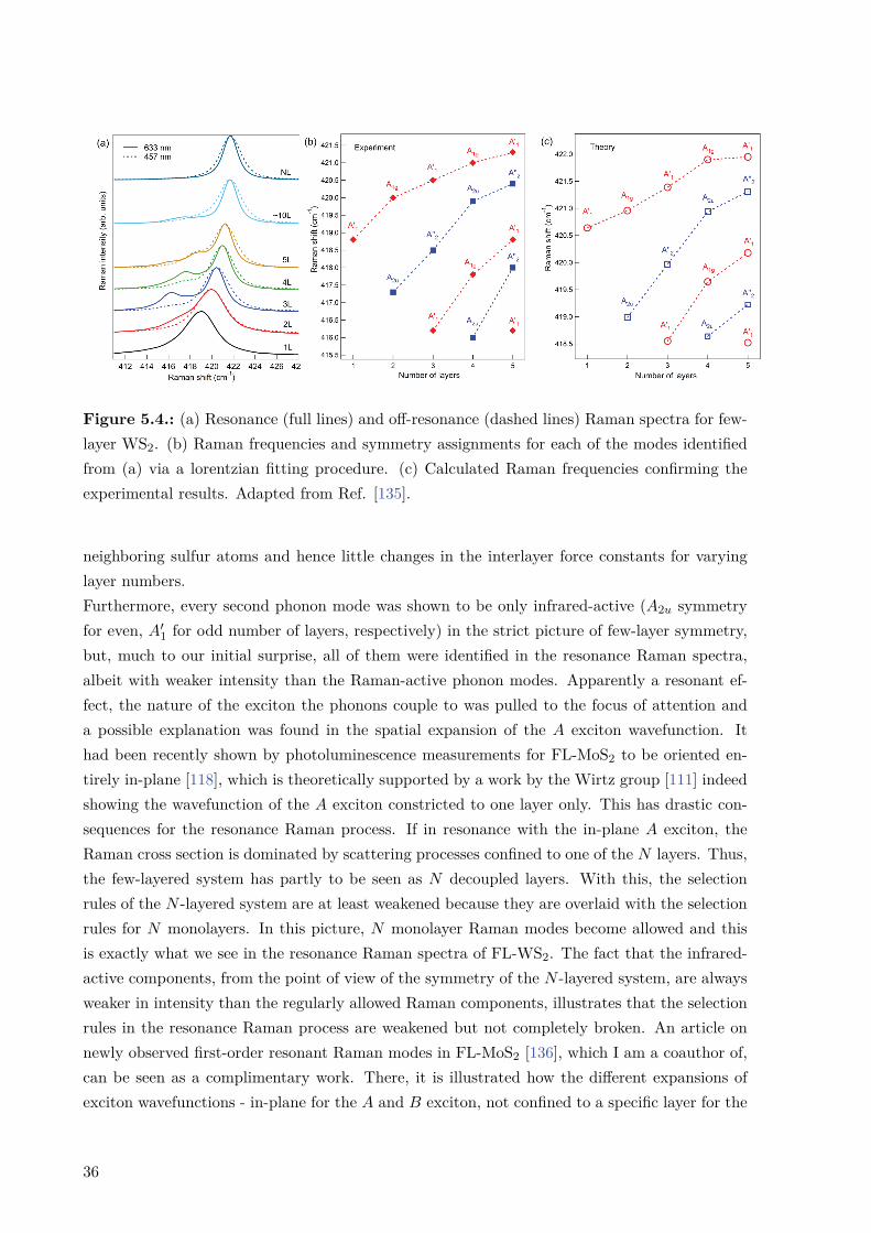
Figure 5.4.: (a) Resonance (full lines) and off-resonance (dashed lines) Raman spectra for few-layer WS2. (b) Raman frequencies and symmetry assignments for each of the modes identifiedfrom (a) via a lorentzian fitting procedure. (c) Calculated Raman frequencies confirming theexperimental results. Adapted from Ref. [135].
neighboring sulfur atoms and hence little changes in the interlayer force constants for varyinglayer numbers.Furthermore, every second phonon mode was shown to be only infrared-active (A2u symmetryfor even, A′
1 for odd number of layers, respectively) in the strict picture of few-layer symmetry,but, much to our initial surprise, all of them were identified in the resonance Raman spectra,albeit with weaker intensity than the Raman-active phonon modes. Apparently a resonant ef-fect, the nature of the exciton the phonons couple to was pulled to the focus of attention anda possible explanation was found in the spatial expansion of the A exciton wavefunction. Ithad been recently shown by photoluminescence measurements for FL-MoS2 to be oriented en-tirely in-plane [118], which is theoretically supported by a work by the Wirtz group [111] indeedshowing the wavefunction of the A exciton constricted to one layer only. This has drastic con-sequences for the resonance Raman process. If in resonance with the in-plane A exciton, theRaman cross section is dominated by scattering processes confined to one of the N layers. Thus,the few-layered system has partly to be seen as N decoupled layers. With this, the selectionrules of the N -layered system are at least weakened because they are overlaid with the selectionrules for N monolayers. In this picture, N monolayer Raman modes become allowed and thisis exactly what we see in the resonance Raman spectra of FL-WS2. The fact that the infrared-active components, from the point of view of the symmetry of the N -layered system, are alwaysweaker in intensity than the regularly allowed Raman components, illustrates that the selectionrules in the resonance Raman process are weakened but not completely broken. An article onnewly observed first-order resonant Raman modes in FL-MoS2 [136], which I am a coauthor of,can be seen as a complimentary work. There, it is illustrated how the different expansions ofexciton wavefunctions - in-plane for the A and B exciton, not confined to a specific layer for the
36
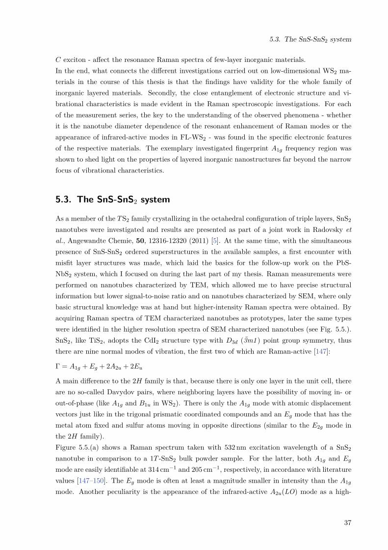
5.3. The SnS-SnS2 system
C exciton - affect the resonance Raman spectra of few-layer inorganic materials.In the end, what connects the different investigations carried out on low-dimensional WS2 ma-terials in the course of this thesis is that the findings have validity for the whole family ofinorganic layered materials. Secondly, the close entanglement of electronic structure and vi-brational characteristics is made evident in the Raman spectroscopic investigations. For eachof the measurement series, the key to the understanding of the observed phenomena - whetherit is the nanotube diameter dependence of the resonant enhancement of Raman modes or theappearance of infrared-active modes in FL-WS2 - was found in the specific electronic featuresof the respective materials. The exemplary investigated fingerprint A1g frequency region wasshown to shed light on the properties of layered inorganic nanostructures far beyond the narrowfocus of vibrational characteristics.
5.3. The SnS-SnS2 system
As a member of the TS2 family crystallizing in the octahedral configuration of triple layers, SnS2
nanotubes were investigated and results are presented as part of a joint work in Radovsky etal., Angewandte Chemie, 50, 12316-12320 (2011) [5]. At the same time, with the simultaneouspresence of SnS-SnS2 ordered superstructures in the available samples, a first encounter withmisfit layer structures was made, which laid the basics for the follow-up work on the PbS-NbS2 system, which I focused on during the last part of my thesis. Raman measurements wereperformed on nanotubes characterized by TEM, which allowed me to have precise structuralinformation but lower signal-to-noise ratio and on nanotubes characterized by SEM, where onlybasic structural knowledge was at hand but higher-intensity Raman spectra were obtained. Byacquiring Raman spectra of TEM characterized nanotubes as prototypes, later the same typeswere identified in the higher resolution spectra of SEM characterized nanotubes (see Fig. 5.5.).SnS2, like TiS2, adopts the CdI2 structure type with D3d (3m1 ) point group symmetry, thusthere are nine normal modes of vibration, the first two of which are Raman-active [147]:
Γ = A1g + Eg + 2A2u + 2Eu
A main difference to the 2H family is that, because there is only one layer in the unit cell, thereare no so-called Davydov pairs, where neighboring layers have the possibility of moving in- orout-of-phase (like A1g and B1u in WS2). There is only the A1g mode with atomic displacementvectors just like in the trigonal prismatic coordinated compounds and an Eg mode that has themetal atom fixed and sulfur atoms moving in opposite directions (similar to the E2g mode inthe 2H family).Figure 5.5.(a) shows a Raman spectrum taken with 532 nm excitation wavelength of a SnS2
nanotube in comparison to a 1T -SnS2 bulk powder sample. For the latter, both A1g and Eg
mode are easily identifiable at 314 cm−1 and 205 cm−1, respectively, in accordance with literaturevalues [147–150]. The Eg mode is often at least a magnitude smaller in intensity than the A1g
mode. Another peculiarity is the appearance of the infrared-active A2u(LO) mode as a high-
37
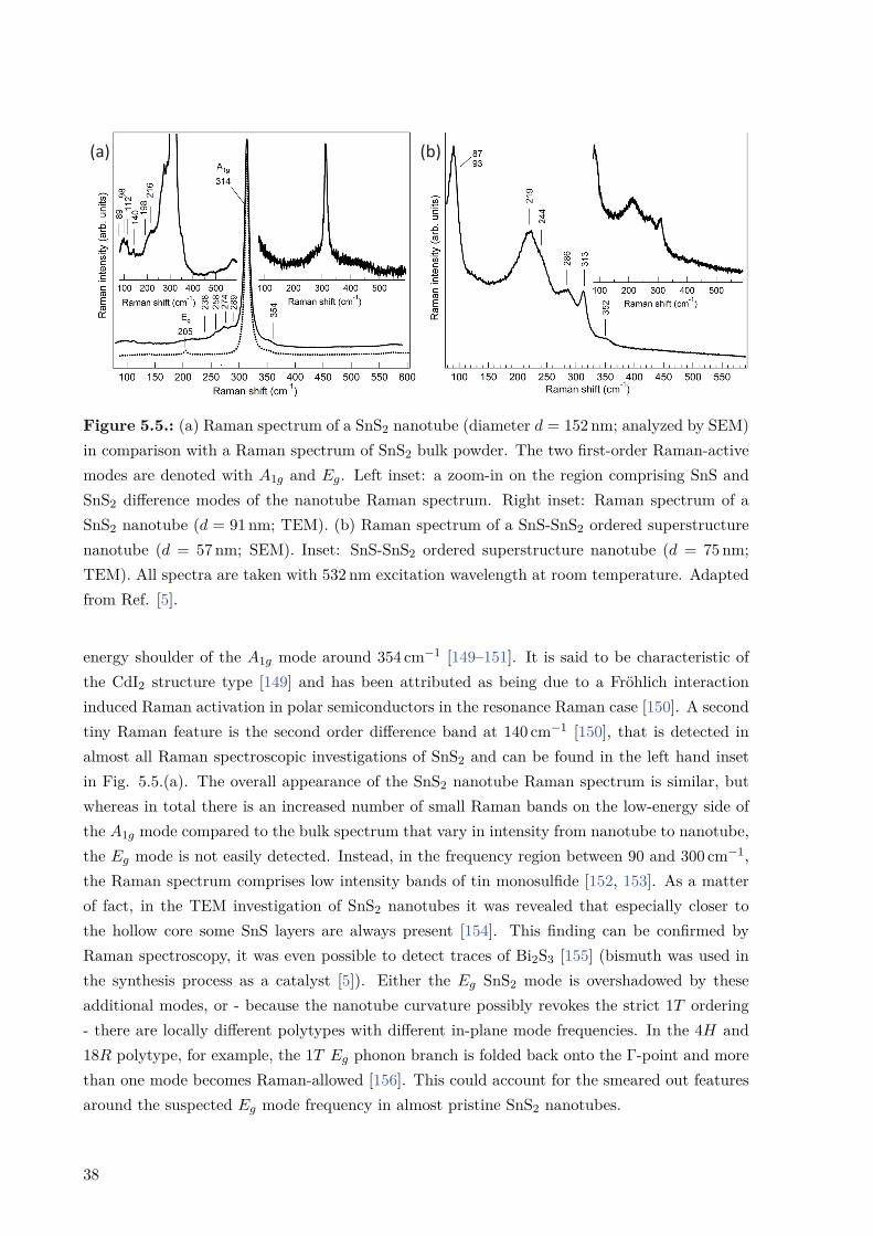
(b)(a)
Figure 5.5.: (a) Raman spectrum of a SnS2 nanotube (diameter d = 152 nm; analyzed by SEM)in comparison with a Raman spectrum of SnS2 bulk powder. The two first-order Raman-activemodes are denoted with A1g and Eg. Left inset: a zoom-in on the region comprising SnS andSnS2 difference modes of the nanotube Raman spectrum. Right inset: Raman spectrum of aSnS2 nanotube (d = 91 nm; TEM). (b) Raman spectrum of a SnS-SnS2 ordered superstructurenanotube (d = 57 nm; SEM). Inset: SnS-SnS2 ordered superstructure nanotube (d = 75 nm;TEM). All spectra are taken with 532 nm excitation wavelength at room temperature. Adaptedfrom Ref. [5].
energy shoulder of the A1g mode around 354 cm−1 [149–151]. It is said to be characteristic ofthe CdI2 structure type [149] and has been attributed as being due to a Fröhlich interactioninduced Raman activation in polar semiconductors in the resonance Raman case [150]. A secondtiny Raman feature is the second order difference band at 140 cm−1 [150], that is detected inalmost all Raman spectroscopic investigations of SnS2 and can be found in the left hand insetin Fig. 5.5.(a). The overall appearance of the SnS2 nanotube Raman spectrum is similar, butwhereas in total there is an increased number of small Raman bands on the low-energy side ofthe A1g mode compared to the bulk spectrum that vary in intensity from nanotube to nanotube,the Eg mode is not easily detected. Instead, in the frequency region between 90 and 300 cm−1,the Raman spectrum comprises low intensity bands of tin monosulfide [152, 153]. As a matterof fact, in the TEM investigation of SnS2 nanotubes it was revealed that especially closer tothe hollow core some SnS layers are always present [154]. This finding can be confirmed byRaman spectroscopy, it was even possible to detect traces of Bi2S3 [155] (bismuth was used inthe synthesis process as a catalyst [5]). Either the Eg SnS2 mode is overshadowed by theseadditional modes, or - because the nanotube curvature possibly revokes the strict 1T ordering- there are locally different polytypes with different in-plane mode frequencies. In the 4H and18R polytype, for example, the 1T Eg phonon branch is folded back onto the Γ-point and morethan one mode becomes Raman-allowed [156]. This could account for the smeared out featuresaround the suspected Eg mode frequency in almost pristine SnS2 nanotubes.
38

5.4. The PbS-NbS2 system
During the work on the SnS-SnS2 system, most often spectra of the type shown in Fig. 5.5.(b)were encountered. The respective nanotubes or nanoscrolls comprise SnS as well as SnS2 layersin different orderings with O-T-T, O-T and O-T-O-T-T as the most common ones (O for theorthorhombic SnS, T for the SnS2 lattice, respectively, see Chapter 2.3.). Here, the questionarose, to what extent the SnS2 mode frequencies are influenced by the presence of SnS layers,or vice versa, and whether this influence scales with the ratio SnS/SnS2. Clearly seen in theexemplary SnS-SnS2 nanotube spectra in Fig. 5.5.(b) is the mode at 313 cm−1 with the shoulderat 352 cm−1 which can be attributed to the A1g and the A2u mode, respectively, of the SnS2 partof the structure, with negligible shift compared to the pristine nanotube. Other than that, thespectrum is dominated by features identifiable as belonging to the SnS layers, again, only smallshifts are observed. The measured spectra of the SnS-SnS2 system are hence a confirmation ofwhat is called the rigid band model in describing the electronic structure of such superstructures:the Raman spectra are to a first approximation a superposition of the Raman features of theconstituents. However, as will be shown later for the PbS-NbS2 system, in misfit layer structures,the in-plane mode of the S-T-S triple layer is a very sensitive indicator of interlayer interaction,and it is just this mode that, just as in the SnS2 case, can not be made out in the SnS-SnS2
nanotube spectra. One has to resort to other pieces of evidence with the small shifts of theout-of-plane modes serving as a first indication of very weak interlayer interaction. Even moreso as no frequency differences were detected neither for different orderings of SnS and SnS2
layers nor for nanotubes and nanoscrolls. To the best of my knowledge there are no Ramanspectroscopic reports on SnS-SnS2, but there is at least one article on lithium-intercalated SnS2.Alkali metals are prone to donate an electron to neighboring layers and since charge transfer isone of the main routes to explain frequency shifts in intercalation compounds like LiTiS2 [157]the existence of only small (up)shifts in LiSnS2 [158] points in the same direction. A recentpaper actually calculates a very small charge transfer of less than 0.1 electrons in the SnS-SnS2
double layer from the SnS2 to the SnS layer [79], contrary to the charge transfer direction that iscommon in other misfit layer systems (see Chapter 3.2.). Finally, the simultaneous and randomoccurrence of different stacking sequences in the SnS-SnS2 nanotube synthesis speaks in favor ofweak interlayer interaction and consequently for at most small frequency shifts in the combinedmaterials.
5.4. The PbS-NbS2 system
Work on misfit nanotubes of the type (PbS)1.14NbS2 and of NbS2 nanotubes intercalated withlead formed the last part of my thesis and results are published in Staiger et al., Physical ReviewB, 94, 035430 (2016). I was already familiar with the specifics of 2H transition metal dichalco-genides and with the basic questions arising when these materials are hosting intercalants andform misfit layer compounds, respectively. But, as it turned out, the situation is entirely dif-ferent from the prior work on the SnS-SnS2 system. 2H-NbS2, like WS2, has the D6h point
39

Figure 5.6.: (a) Raman spectra of an exemplary (PbS)1.14NbS2 and a PbNbS2 nanotube.The main in-plane and out-of-plane modes are located around 350 and 380 cm−1, respectively.(b) A closer look reveals subtle differences in the frequency of the Raman modes and theirrespective symmetry. Both spectra are taken taken with 532 nm excitation wavelength at roomtemperature.
group and the frequencies of the main A1g and E2g Raman modes are around 379 and 309 cm−1,respectively [159]. In the misfit layer nanotubes, because the NbS2 layers are separated by aPbS layer in between, is is more accurate to make use of the monolayer D3h symmetry, not ac-counting for additional structural distortion induced by the intercalant layer and the nanotubecurvature. For the measured nanotubes the two Raman modes related to the A1g and E2g modeof the parent material were identified at 378 (A′
1) and 353 cm−1 (E′). In the PbNbS2 nanotubes,where the parent material symmetry is approximately retained, the same modes were observedat 377 (A1g) and 348 cm−1 (E2g). Raman spectra of the two cases are shown in Fig. 5.6. Thus,two main characteristics are seen to distinguish the experimental observations from the resultsobtained for the SnS-SnS2 nanotubes. The in-plane E mode is clearly detected in the spectraand is seen to shift up drastically with respect to the parent material, whereas the frequency ofthe out-of-plane A mode stays almost the same. Clearly, the key to the understanding of thisquite unusual strength of frequency shifts has to be found in the characteristics of the interlayerinteraction when combining the two materials. Some basic concepts of interlayer interactionhave been presented in Chapter 3.2. of this thesis. Niobium disulfide intercalated with leadhas not been investigated by Raman spectroscopy before, but while the same holds true for(PbS)1.14NbS2 nanotubes, the bulk misfit system as well as a variety of other misfit layer sys-tems and intercalated layered systems have been subject of research [20, 157, 159–169]. Forcompounds containing NbS2 and intercalants other than rare earth metal monochalcogenides
40

5.4. The PbS-NbS2 system
the results are similar to the ones presented here, a strong upshift for the in-plane and littleto no change for the out-of-plane mode of the TMD part of the structure is measured [159–162, 166]. Yet, despite intensive discussion and authors presenting several, partly contradictingmodels, no definite conclusion has been reached as to why this mode-stiffening only occurs forthe in-plane Raman mode. Moreover, for NbS2 misfit layer compounds with rare earth metalmonochalcogenides even the out-of-plane A′
1 mode shifts up and extra modes start appearingthat can not be explained in the context of the simple superposition of Raman modes of theconstituents [20, 164]. In contrast, in MLCs containing 1T -TMDs and in intercalated 1T -TMDs,several authors claim to observe a small downshift of the Eg mode with respect to the parentmaterial [157, 160].Assuming the reasons for the frequency changes are based on the same underlying mechanismfor all these compounds, in finding an explanation for the frequency shifts in PbNbS2 and(PbS)1.14NbS2 nanotubes, one has to aspire to bring under the same umbrella also the phenom-ena observed in other misfit and intercalated layered compounds. The mechanism put forwardby a majority of authors for the NbS2 compounds is that a filling of the NbS2 dz2 orbital bycharge transfer from the intercalant is to be held responsible for the raise in frequency. However,it is not clear why this charge transfer should have a larger impact on the E mode frequencyand only little impact on the A mode frequency in MXNbS2. One idea was to consider theorientation of the main lobe of the dz2 orbital: it is oriented perpendicular to the layers, thusthe atomic displacements for an in-plane vibrational mode will lead to changes in the chalco-gen valence / transition metal dz2 orbital overlap and lead to a subsequent frequency upshift,whereas the same change will not occur for out-of-plane modes [168]. This model can not beapplied simultaneously to 1T misfit layer compounds, where small E mode downshifts occur.One has to take into account though that the 1T -TMD orbital the charge is transferred to fromthe intercalant does not have the same orientation than the trigonal prismatic dz2 orbital. Adifferent approach is presented by Shirai et al. [169] and focuses on the changes of intralayercentral and noncentral forces upon charge transfer. Again, this model only deals with trigonalprismatic TX2 compounds and is not applicable to the 1T family.If the charge transfer mechanism was to be held accountable to the frequency upshift in trig-onal prismatic MLC, as a second assumption, the magnitude of the former should be relatedto the strength of the latter, e.g. large charge transfer should make for large frequency up-shifts. Looking at the literature, comparing MSNbS2 [160] and RSNbS2 [161] this seems tobe indeed the case, also stage 2 compounds, where a RS layer is inserted only every secondNbS2 layer and hence a smaller charge transfer is likely, exhibit smaller frequency upshifts thanstage 1 compounds [20]. Having two model systems, PbNbS2 nanotubes (upshift: 39 cm−1) and(PbS)1.14NbS2 (upshift: 44 cm−1) the magnitude of the charge transfer should thus be similar.As a matter of fact though, as was carried out in detail in Chapter 3.2., the charge transferexpected for (PbS)1.14NbS2 - if there at all - is only a small fraction of the larger charge transferconfirmed for the intercalation compound PbNbS2. The measured frequency upshifts are hencenot likely to be caused by charge transfer.
41
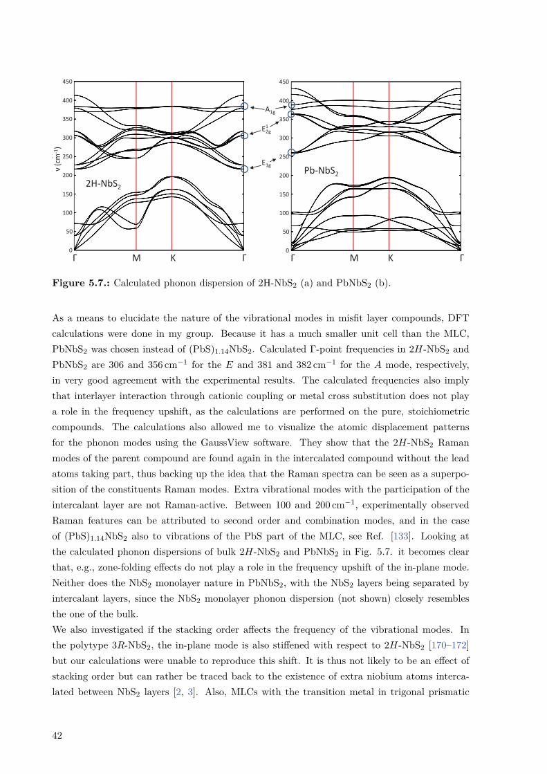
Γ Γ Γ ΓM MK K
2H-NbS2Pb-NbS2
E1g
A1g
E2g1
0
50
100
150
200
250
300
350
400
450
0
50
100
150
200
250
300
350
400
450
ν(cm
-1)
Figure 5.7.: Calculated phonon dispersion of 2H-NbS2 (a) and PbNbS2 (b).
As a means to elucidate the nature of the vibrational modes in misfit layer compounds, DFTcalculations were done in my group. Because it has a much smaller unit cell than the MLC,PbNbS2 was chosen instead of (PbS)1.14NbS2. Calculated Γ-point frequencies in 2H-NbS2 andPbNbS2 are 306 and 356 cm−1 for the E and 381 and 382 cm−1 for the A mode, respectively,in very good agreement with the experimental results. The calculated frequencies also implythat interlayer interaction through cationic coupling or metal cross substitution does not playa role in the frequency upshift, as the calculations are performed on the pure, stoichiometriccompounds. The calculations also allowed me to visualize the atomic displacement patternsfor the phonon modes using the GaussView software. They show that the 2H-NbS2 Ramanmodes of the parent compound are found again in the intercalated compound without the leadatoms taking part, thus backing up the idea that the Raman spectra can be seen as a superpo-sition of the constituents Raman modes. Extra vibrational modes with the participation of theintercalant layer are not Raman-active. Between 100 and 200 cm−1, experimentally observedRaman features can be attributed to second order and combination modes, and in the caseof (PbS)1.14NbS2 also to vibrations of the PbS part of the MLC, see Ref. [133]. Looking atthe calculated phonon dispersions of bulk 2H-NbS2 and PbNbS2 in Fig. 5.7. it becomes clearthat, e.g., zone-folding effects do not play a role in the frequency upshift of the in-plane mode.Neither does the NbS2 monolayer nature in PbNbS2, with the NbS2 layers being separated byintercalant layers, since the NbS2 monolayer phonon dispersion (not shown) closely resemblesthe one of the bulk.We also investigated if the stacking order affects the frequency of the vibrational modes. Inthe polytype 3R-NbS2, the in-plane mode is also stiffened with respect to 2H-NbS2 [170–172]but our calculations were unable to reproduce this shift. It is thus not likely to be an effect ofstacking order but can rather be traced back to the existence of extra niobium atoms interca-lated between NbS2 layers [2, 3]. Also, MLCs with the transition metal in trigonal prismatic
42

5.4. The PbS-NbS2 system
coordination in CC [e.g. (SnS)1.17NbS2] or CF [e.g. (PbS)1.14NbS2] stacking order [13] (seeFig. 2.2.) seem to exhibit the same frequency trends. This is further supported by calculationsdone at the Jacobs university in Bremen, where a single slab of NbS2 sandwiched between twolead atom layers, without the influence of any neighboring NbS2 layers, was shown to exhibit asimilar strength of frequency upshift [173].The existence of covalent bonds between intercalant and TMD layers is under debate (see Chap-ter 3.2.) but one would expect them to act more strongly on the frequency of in-plane thanout-of-plane modes.A model not discussed yet in the literature on misfit layer compounds takes into account thecharge redistribution in the intercalant layers during the atomic vibrations. In the NbS2 in-planeE mode the movement of negatively charged sulfur atoms along the layer direction will lead to arearrangement of charges also in the adjacent intercalant layer. In order to restore equilibrium,this charge redistribution will, in turn, act as a restoring force on the sulfur atoms and conse-quently raise the frequency of the respective vibration. In the case of the out-of-plane A mode,because significant charge redistribution will not occur perpendicular to the layer direction or isnot possible at all in one-atom thick intercalant layers, the frequency remains unaffected. Thishypothesis was tested for (PbS)1.14NbS2 with the finite displacement frozen phonon technique.There, the atomic displacement pattern is divided into small steps and each time the forcesacting on the atoms taking part in the vibration is calculated, thus taking into considerationthe effect of a possible charge redistribution on the Raman frequencies. Carried out in detailin Ref. [133] the calculations indeed favor this new model, as the in-plane E mode frequenciesare raised strongly and the out-of-plane A mode frequency exhibits only a small downshift withrespect to the parent material. Calculations have yet to be performed for semiconducting groupIVB compounds in octahedral coordination, where a small downshift for the in-plane mode isseen in the MLCs, thus the question whether the above described concept has validity for allMLCs remains an open question.In conclusion, the misfit layer systems represent a family of materials, where Raman spectro-scopic investigations can yield a lot of information also about the electronic properties. As misfitlayer nanotubes have only been synthesized for the first time in recent years [5, 6, 45, 46, 56,174, 175] further research on the vibrational properties will be of great value.
43

Summary and outlook6
In this thesis, I studied nanostructures of inorganic layered materials by Raman and ResonanceRaman spectroscopy. Research was done almost always on individual nanostructures with priorcharacterization by electron microscopy techniques (see Appendix A.1.). Investigated com-pounds cover all dimensionalities, a variety of materials are combined in misfit layer structuresand different stacking types occur in the pristine and misfit compounds. Yet, I was able to showthat the discussion of the vibrational properties relies on a few principles that are common to allthe studied materials. Furthermore, research revealed just how closely vibrational and electronicproperties are intertwined.By virtue of their triple-layered nature all of the vibrational modes in transition metal dichalco-genides have the atoms either moving out of plane in the stacking c direction or doubly degener-ated in the ab-plane. Within the triple layers there are two basic coordinations possible for thetransition metal atom in the middle layer, for the group IVA and IVB TMDs this is the octahe-dral coordination, for the majority of group VB and VIB TMDs it is the trigonal prismatic one.In the octahedrally coordinated compounds there are only two Raman active modes, an out-of-plane A1g mode and an in-plane Eg mode (see Fig. 5.1.). In the bulk structure of the latter, ofthe four Raman active vibrations, the rigid layer E2
2g mode is of very low frequency and the E1g
principally not allowed in the employed backscattering configuration. This leaves the in-planeE1
2g and again an out-of-plane A1g mode as the main fingerprint modes in trigonal prismaticallycoordinated compounds. These two Raman modes are at the core of every study conducted inthe course of this thesis and their characteristics are followed with different dimensionality andstacking order changes, with changes in excitation energy and experimental parameters.I performed Raman spectroscopy on low-dimensional WS2, MoS2 and SnS2 materials and misfitlayer/intercalation compounds SnS-SnS2, PbNbS2 and (PbS)1.14NbS2. It was the investigationof the A1g mode that in the case of the former revealed the most information, not only about thevibrational characteristics of inorganic layered structures but about their electronic structure aswell, especially the nature of the excitons. In the case of the misfit/intercalation compounds,in contrast, the E1
2g/Eg Raman mode was the primary study object and interlayer interactionproved to be the pivotal point of discussion. Thus, obtained results can be divided in two partsas follows:
44
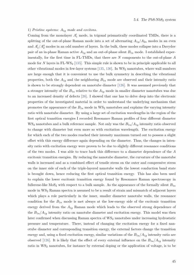
5.4. The PbS-NbS2 system
1) Pristine systems: A1g mode and excitons.Coming from the monolayer A′
1 mode, in trigonal prismatically coordinated TMDs, there is asplitting of the out-of-plane Raman mode into a set of alternating A1g/A2u modes in an evenand A′
1/A′′2 modes in an odd number of layers. In the bulk, these modes collapse into a Davydov
pair of an in-phase Raman active A1g and an out-of-phase silent B1u mode. I established exper-imentally, for the first time in FL-TMDs, that there are N components to the out-of-plane A
mode for N layers in FL-WS2 [135]. This simple rule is shown to be in principle applicable to allother vibrational modes in few-layer systems [135, 136]. In WS2 nanotubes, where wall numbersare large enough that it is convenient to use the bulk symmetry in describing the vibrationalproperties, both the A1g and the neighboring B1u mode are observed and their intensity ratiois shown to be strongly dependent on nanotube diameter [126]. It was assumed previously thata stronger intensity of the B1u relative to the A1g mode in smaller diameter nanotubes was dueto an increased density of defects [26]. I showed that one has to delve deep into the electronicproperties of the investigated material in order to understand the underlying mechanism thatpromotes the appearance of the B1u mode in WS2 nanotubes and explains the varying intensityratio with nanotube diameter. By using a large set of excitation wavelengths in the region of thefirst optical transition energies I recorded Resonance Raman profiles of four different diameterWS2 nanotubes and a bulk reference sample. Not only was the B1u/A1g intensity ratio observedto change with diameter but even more so with excitation wavelength. The excitation energyfor which each of the two modes reached their intensity maximum turned out to possess a slightoffset with this energy difference again depending on the diameter. Thus, the changes in inten-sity ratio with excitation energy were proven to be due to slightly different resonance conditionsof the two modes. I was able to trace back this difference to a diameter dependence of the A
excitonic transition energies. By reducing the nanotube diameter, the curvature of the nanotubewalls is increased and as a combined effect of tensile stress on the outer and compressive stresson the inner side of each of the triple-layered nanotube walls the lowest conduction band stateis brought down, hence reducing the first optical transition energy. This has also been usedto explain the lower excitonic transition energy found by Resonance Raman spectroscopy infullerene-like MoS2 with respect to a bulk sample. As the appearance of the formally silent B1u
mode in WS2 Raman spectra is assumed to be a result of strain and mismatch of adjacent layerswhich plays a role particularly in the inner, smaller diameter nanotube walls, the resonancecondition for the B1u mode is met always at the low-energy side of the excitonic transitionenergy derived from the A1g Raman mode which leads to the observed strong dependence ofthe B1u/A1g intensity ratio on nanotube diameter and excitation energy. This model was thenlater confirmed when discussing Raman spectra of WS2 nanotubes under increasing hydrostaticpressure and temperature. There, instead of changing the excitation energy for a fixed nan-otube diameter and corresponding transition energy, the external factors change the transitionenergy and, using a fixed excitation energy, similar variations of the B1u/A1g intensity ratio areobserved [126]. It is likely that the effect of every external influence on the B1u/A1g intensityratio in WS2 nanotubes, for instance by external doping or the application of voltage, is to be
45
explained along similar lines. A recent work [176] is in excellent agreement with the observedpressure dependence of Raman modes, particularly of the A1g mode, in WS2 nanotubes andconfirms the findings presented in this thesis.In the resonance Raman spectra of FL-WS2 all of the N components to the out-of-plane mode,Raman-active and formally infrared-active ones, are detected. Again, this can only be explainedby the specifics of the electronic structures of the investigated TMDs, particularly the nature ofthe excitons. The activation of infrared-active phonons in the Raman spectra is an indicationof a relaxation of Raman selection rules. The model put forward in my work on FL-WS2 isevidence of the in-plane orientation of the A exciton in FL-TMDs confirming recent studies[111, 118]. In a simple picture, during the resonance Raman process the phonons couple to onelayer only and are thus subjected to the selection rules of N partly decoupled layers. As a result,selection rules in the N layered system are weakened and low-intensity infrared-active phononsare observed in the Raman spectra. As Ref. [136] points out, this will likely not be the case formeasurements in resonance with the C exciton which is found to be stretched out in all threedimensions. Recently, we identified first-order Raman modes in FL-MoS2 that only appear withconsiderable intensity when the sample is excited in resonance with the C exciton [136]. Theinsights presented should be transferable to FL-WS2 as well, where first measurements indicateagain a fine structure of these modes that is not seen in FL-MoS2.
2) Misfit/intercalation systems: E12g/Eg mode and interlayer interaction.
As an introductory work to Raman spectroscopy on misfit layer nanotubes, Raman spectra ofalmost pristine SnS2 and SnS-SnS2 misfit nanotubes were compared. I was able to prove thatthe misfit system spectra can be interpreted in terms of a superposition of the Raman modes ofthe constituents. Almost identical A1g mode frequencies in the two compounds lead me to theconclusion that interlayer interaction was weak in the misfit system, a result that was later con-firmed by theoretical studies [79]. However, the in-plane SnS2 Eg mode was not identified in theSnS-SnS2 spectra. The related in-plane E1
2g of the trigonal prismatic compounds turned out tobe the most sensitive indicator of interlayer interaction in misfit layer systems, so it would be ofinterest whether under certain experimental conditions the Eg mode in SnS-SnS2 is discernible.This could be the use of a different excitation energy or low-temperature measurements.In the main work on misfit layer nanotubes, the system PbNbS2 and (PbS)1.14NbS2 was thor-oughly investigated. In comparison with literature data on the parent 2H-NbS2 material I ob-served a drastic upshift of the in-plane modes in the misfit/intercalated nanotubes and a nearlyconstant out-of-plane A mode frequency. The charge transfer mechanism held accountable forthis shifts by a majority of previous studies was put to the test and shown to not satisfactorilyexplaining the similar in-plane E mode upshifts in both PbNbS2 and (PbS)1.14NbS2 nanotubes.As charge transfer is weaker in (PbS)1.14NbS2 than in PbNbS2 but the upshift is slightly strongerin the former, this apparent contradiction calls for an alternative approach. A number of inter-layer interaction mechanisms such as non-stoichiometry, metal cross substitution and covalentbonding as well as Raman spectra of other misfit compounds were discussed. To support the
46
5.4. The PbS-NbS2 system
experimental results, a number of DFT calculations on 2H-NbS2 and PbNbS2 were performedand found to be in very good agreement with experiment. In the end, finite-displacement frozenphonon calculations on the PbS-NbS2 system provided evidence that during in-plane movementof the NbS2 part charge in the adjacent PbS layer is being redistributed and the resulting restor-ing forces raise the in-plane frequency through interlayer interaction.The PbS-NbS2 system is only an example of the ever growing number of misfit layer nanos-tructures. Raman studies on newly synthesized MS-TaS2 [46] nanotubes, judging from theirsimilarity to the structural and electronic properties of MS-NbS2, are likely to yield similarresults. In contrast, research on misfit systems should continue in the direction of lanthanide-based misfit nanotubes like LnS-TaS2 NTs [174] and especially nanotubes where the transitionmetal dichalcogenide is CrS2 [45, 56, 175]. For these compounds charge transfer is establishedand could well lead to additional shifts in the Raman spectra. Moreover research on CrS2-basedmisfit compounds should present an interesting experimental and theoretical challenge as thelayered bulk CrS2 compound is not known to exist.
47


Appendices


A. Experimental methods
A.1. Experimental procedure
Apart from the experiments on few-layer WS2, the work in this thesis was largely done in col-laboration with the group of Prof. Tenne at the Weizmann Institute of Science (WIS) in Israel.This group specializes in the synthesis and characterization of inorganic nanotubes and hasdone a vast amount of pioneering work in the field. The joint goal of this collaboration was toinvestigate individual inorganic nanotubes by Raman spectroscopy with simultaneous preciseknowledge of their inner structure. This method differs from the way Raman spectroscopicinvestigations are normally carried out on carbon nanotubes, where one is challenged to ex-tract knowledge about different diameter and chirality nanotubes from ensemble measurements.Having all the structural information prior to Raman measurements allowed me to be sensitiveto details like the small differences in Raman frequency of the in-plane mode of PbNbS2 and(PbS)1.14NbS2 nanotubes. As several nanotube types also in the SnS-SnS2 system are oftensynthesized in the same batch, in the future, with one simple Raman measurement one willbe able to distinguish between the different types. Most of the nanotubes investigated herewere synthesized by Gal Radovsky, a PhD student in Prof. Tennes group at the time, whom Iworked most closely with. During the time of our collaboration we developed an understandingof each others work and, most importantly, ways to simplify the Raman measurement process.In the end, when I received new samples from Gal they had already been characterized by scan-ning electron microscopy (SEM), transmission electron microscopy (TEM), electron diffraction,energy-dispersive X-ray spectroscopy (EDS) and had been marked on the underlying substrateby focused ion beam deposition (FIB), so that I was able to begin my work with all the in-formation necessary. In Fig. A.1.(a) an exemplary SnS-SnS2 nanotube on a carbon coated Cusubstrate is shown, surrounded by a platinum circle and a roman cipher to have a commonnumbering, together with a high resolution TEM picture that identifies the nanotube to be ofthe O-T-T type and a complimentary diffraction image. Starting from an easy-to-identify centerof the sample, with the help of a low magnification SEM map with an overlaid Cartesian planeindicating the location of each of the nanotubes, I was able to quickly find the desired positionunder the optical microscope and start the Raman measurements. As it became evident thatthe originally used TEM substrate was especially prone to be ruptured due to laser heating, thethen used Si3N4 nitride TEM grid allowed for slightly higher laser powers without damaging thesubstrate. To make sure that neither the focused ion beam deposition of platinum circles nor
51

A. Experimental methods
(a) (b)
Figure A.1.: (a) Individual nanotubes were placed on a TEM grid, encircled and numbered withFIB deposition. Supplementary information like the high resolution TEM image, the line profileand the diffraction image shown in the insets were available prior to the Raman spectroscopicinvestigation (picture from Ref. [5] Supporting Information). (b) Before performing Ramanspectroscopy, I identified few-layer flakes of WS2, like the one shown here, under the opticalmicroscope.
the TEM analysis did damage or change the structure of the nanotubes, in the beginning of thejoint work, an exemplary WS2 nanotube that had only been characterized by SEM was sent toBerlin, where we performed Raman measurements before sending it back for TEM characteriza-tion in Israel (operation power was 120 keV). As shown in Ref. [126], a Raman spectrum takenafter the nanotube was again sent to Berlin did not show any of the Raman features altered inany way. Thus, from then on, nanotubes were routinely analyzed by TEM before performingRaman measurements. In the framework of a soon to begin GIF (German-Israeli Foundation forScientific Research and Development) project we envision to extend this mode of collaborationby studying the individual nanotubes sequentially by moving them from the WIS to the TUBerlin and then to Jülich for Cs corrected TEM/STEM analysis.In the case of the work on WS2 nanotubes the focus did not lie so much on the TEM character-ization. For establishing the diameter dependence of the first optical transition energy [126] itwas only necessary to prepare individual nanotubes, making sure by SEM characterization thata larger range of diameters was covered. The same applied for the unpublished work on thediameter dependence of the strength of the antenna effect. During the work on SnS2 and SnS-SnS2 nanotubes, TEM characterization was established as a complimentary tool to the Ramanmeasurements, as from both methods differences between pure SnS2 and misfit layer nanotubesas well as mixed cases were unambiguously identified. Finally, for research on the misfit PbS-NbS2 system, the combination of TEM and Raman investigations was absolutely vital. Moreor less as a side product, together with (PbS)1.14NbS2 nanotubes, PbNbS2 nanotubes had been
52

A.2. Raman spectroscopy: experimental details
synthesized which were detected in the TEM images because of the different periodicity of thelayers. In the Raman spectra, the two types exhibit very similar features and without the priorknowledge could have been easily mistaken for one and the same sort of misfit nanotubes. Be-ing aware of the difference made me sensitive to the small differences in Raman frequencies ofrelated modes. Now, not only does one single Raman measurement suffice to tell whether onehas a real misfit layer nanotube at hand or a nanotube intercalated with lead (often both typesare synthesized in the same batch). Moreover, the two model systems were an interesting studyobject to test traditional beliefs in explaining the unusually high frequency shifts with respectto the transition metal dichalcogenide parent material [133].For my work on few-layer WS2 I received samples from the University Duisburg-Essen, where aWS2 crystal acquired from hq graphene, Netherlands - Groningen had been mechanically exfoli-ated onto an SiO2/Si wafer. I then searched the wafer for appropriate WS2 flakes and identifiedapproximate layer numbers by optical contrast measurements prior to Raman measurements.One example of such a flake is depicted in Fig. A.1.(b). After the Raman measurements, layernumbers were confirmed by atomic force microscopy scans.
A.2. Raman spectroscopy: experimental details
Raman spectra of low-dimensional transition metal dichalcogenides were acquired, with theexception of pressure and temperature measurements, at ambient conditions and always inbackscattering geometry. Apart from the work on MoS2 inorganic fullerenes where ensemblemeasurements in solution were done in a macro-optic setup, confocal μ-Raman spectroscopy ofindividual nanoparticles was the method of choice. The work on WS2 nanotubes was largely doneemploying a triple monochromator Dilor XY800 Raman system with a 1800 lines/mm gratingin subtractive mode, a 100x objective (numerical aperture of NA= 0.95) and a nitrogen-cooledcharge-coupled device. The acquisition of Resonance Raman profiles required a combination ofdifferent laser excitation energies - for this undertaking an ArKr ion laser, a variable frequencydye laser (DCM dye) and a TiSa solid-state laser were used to cover the whole WS2 A and B
excitonic energy range. Measurements were always done such that the nanotube orientation wasparallel to the linear polarization of the incoming laser light. The limitation of laser excitationpower to less than 150 μW to avoid sample heating brought with it accumulation times of 30to 300 s. In order to be able to compare WS2 NT Raman cross sections depending on theexcitation energy, the non-resonant Raman signal of CaF2 was recorded after each nanotubeRaman measurement.Raman measurements on FL-WS2 were performed with a LabRAM HR800 Raman spectrometerequipped with notch filters suppressing the Rayleigh scattered light. A diode laser emitting at457 nm was used for off-resonance Raman and a HeNe laser with an excitation wavelengthof 633 nm for resonance WS2 Raman measurements. The other experimental conditions weresimilar to the WS2 nanotube measurements. In addition to the high spectral resolution of
53

A. Experimental methods
less than 1 cm−1 I made use of the subpixel mode offered by the LabSpec acquisition software(detailed description, see Ref. [135]) that by providing more data points per wavenumber gave anoverall rounder shape to the Raman peaks, which was of high value in the fitting procedure. TheSnS-SnS2 nanotubes were also investigated using a LabRAM HR800 Raman spectrometer andin this case the laser system chosen was a frequency doubled Nd:YAG laser emitting at 532 nm,closer to the optical transition energies of SnS2 than the red excitation wavelengths used for theWS2 materials. Here, special care had to be taken for the measurements of nanotubes placed noton the standard SiO2 substrate but on TEM grids, where the carbon coated copper substratewas prone to rupturing and laser powers had thus to be reduced to 120 μW and less. The sameheld true for the TEM characterized NbS2-based misfit layer nanotubes. Due to them beingrather poor Raman scatterers (partly because of the metallic nature of NbS2) the 1800 lines/mmwas exchanged for a 600 lines/mm grating to achieve higher signal-to-noise ratio at the expenseof a lower spectral resolution of around 2 cm−1. Accumulation times were still high and exceeded20 minutes in most cases.The pressure Raman measurements on agglomerated WS2 nanotubes were performed by PeterRafailov using a gasketed diamond-anvil cell. Details can be found in Ref. [126]. For temperaturemeasurements I used a Linkam heating and freezing stage, the coolant was liquid nitrogen. Sincethe objective-sample distance was bigger than in the other experiments, a far-distance objective(80x magnification, NA= 0.75) came to use.For all Raman measurements performed in this thesis, the known spectral lines of a neon lampwere used as a calibration standard.
A.3. Basics of Raman spectroscopy
One of the ways light interacts with matter is through scattering processes. Thereby the lightis either scattered elastically (e.g. by defects) and retains its energy or inelastically, losing orgaining a quantized portion of energy in the event. This latter process is called Raman effectafter its discoverer, C.V. Raman [177, 178], who went on to receive the Nobel prize in physicsin 1930. Today, it is one of the primary experimental methods especially in solid state physics.Its contactless and non-destructive nature and the wealth of information the spectra have tooffer makes it an ideal analysis tool for research on novel materials and Raman spectroscopy hastherefore been the main method of choice in this thesis.Let us consider an electromagnetic wave traveling through a medium
�E(�r, t) = �E(�ki, ωi) · cos(�ki · �r − ωit) (A.1)
54

A.3. Basics of Raman spectroscopy
�E(�r, t) will induce a time-dependent polarization �P (�r, t) in the medium with the same frequencyωi and wavevector �ki,
�P (�r, t) = �P (�ki, ωi) · cos(�ki · �r − ωit) (A.2)
The strength of the polarization is determined by the material’s electric susceptibility χ, whichcan be altered periodically by atomic vibrations that are excited thermally at temperatures abovezero. The amplitude of these vibrations �u(�q, ω0), with wavevector �q and vibrational frequencyω0, is normally much smaller than the lattice constants of the material. This allows us to expandχ in a Taylor series with respect to the atomic vibrations �u(�r, t)=�u(�q, ω0)·cos(�q · �r − ω0t)
χ(�ki, ωi, �u) = χ0(�ki, ωi) + δχ
δ�u 0�u(�r, t) + ... (A.3)
where the first term is an expression of the unperturbed susceptibility χ0 and the second termrepresents the perturbation of the susceptibility by the atomic vibrations. The induced polar-ization of the material through the propagating electromagnetic wave can thus be decomposedinto a polarization wave P0 that is in phase with the incident radiation and two polarizationwaves P ±
ind where the atomic vibrations increase or decrease the frequency and wavevector ofthe incident radiation. This is expressed by [179]:
�P = P0 + P ±ind = χ0(�ki, ωi) · �E(�ki, ωi) · cos(�ki · �r − ωit) + (A.4)
12(δχ
δ�u)0�u(�q, ω0) · �E(�ki, ωi) × [cos((�ki + �q) · �r − (ωi + ω0)t) + cos((�ki − �q) · �r − (ωi − ω0)t)]
The first term describes the elastic Rayleigh scattering; the electromagnetic wave travels throughthe medium basically unperturbed. The second term describes the inelastically Raman scatteredlight; the electromagnetic wave leaving the medium has its frequency and wavevector altered byvirtue of the modulation of the electric susceptibility by the atomic vibrations. Either it hasits wavevector and frequency decreased by �kS = (�ki − �q) and ωS = (ωi − ω0) (Stokes radiation)or increased by �kAS = (�ki + �q) and ωAS = (ωi + ω0) (anti-Stokes radiation). As an importantcondition, Raman scattering will only occur in a material if the polarizability changes duringthe lattice vibration - (δχ/δ�u)0 �= 0 - as can be seen from Equation A.4.From a microscopic point of view, the atomic vibrations, much like the photons of the electro-magnetic wave, have particle like character, are quantized, and are commonly called phonons.The Raman scattering is a three-step process involving photons, electrons and phonons. First,an incident photon with energy �ωi excites an electron into an intermediate (either virtual orexcited) state, creating an electron-hole pair. Subsequently, this electron-hole pair now can me-diate between the incident photon and the atomic vibrations and is scattered in another statethereby generating or annihilating a quantized phonon. Finally, electron and hole recombineand a scattered photon �ωs = �(ωi ± ωph) is sent out that has its energy diminished (Stokes-
55

A. Experimental methods
ħ ωi ħ ωi ħ ωi
ħ ω0
ħ ω0
ħ ωiħ (ωi - ω0) ħ (ωi + ω0)
RayleighStokes anti-Stokes
Figure A.2.: Sketch of the Raman process in comparison with the Rayleigh process, where nophonons are involved, in the middle. In the Stokes case a phonon is created and the outgoinglight has a smaller energy than the incoming, in the anti-Stokes process a phonon is annihilatedand the outgoing light possesses a higher energy. Starting from the ground state (solid line), allother states (dashed lines) can either be real (resonant case, see Fig. A.3.) or virtual.
process) or enlarged (anti-Stokes-process) by the energy of a phonon. This is schematicallydepicted in Fig. A.2. with the Rayleigh process, where no phonon is involved in the elasticscattering process, shown in the middle for comparison. While the Rayleigh process is by farthe dominant one in light scattering by solids, Stokes scattering normally has a higher crosssection than anti-Stokes scattering because, as a necessary condition for the anti-Stokes processto occur, a phonon must already be excited in the material in order to be annihilated in theRaman process. In this thesis, Stokes scattering of inorganic nanomaterials is recorded and theRaman shift between the frequency of the incoming and the outgoing photon is measured inreciprocal centimeters (cm−1).The relationship ω(�qph) between the phonon’s frequency ωph and momentum �qph is called phonondispersion and allows one to track the energy of a phonon principally anywhere in the Brillouinzone of a material (see Fig. 5.7.). As Raman scattering requires energy and momentum conser-vation,
�ωi − �ωs ± ωph = 0, ��ki − ��ks ± �qph = 0 (A.5)
using visible light where the photons’ momentum is much smaller than the dimension of theBrillouin zone, Raman scattering as employed in this thesis only probes zone-center Γ-pointphonons with �qph ≈ 0. Still, the Raman spectral features offer a unique fingerprint of a ma-terial and one can follow any outside influence, be it temperature, pressure, strain or atomicimperfections by simply looking at the vibrational frequencies.
56

A.4. Basics of Resonance Raman spectroscopy
incomingnon-resonant outgoing
ħ (ωi - ω0) ħ ωi
ħ ω0
ħ (ωi - ω0) ħ ωi
ħ ω0
ħ (ωi - ω0)ħ ωi
Figure A.3.: Sketch of the Resonance Raman process in comparison with the non-resonantStokes process on the left. Either the incoming light excites the electron into a real state(solid line, incoming resonance) or a real state is hit after a phonon has been created (outgoingresonance). In both cases, the Raman intensity is resonantly enhanced.
A.4. Basics of Resonance Raman spectroscopy
The information that one can extract from the characteristic phonon frequencies is not every-thing Raman spectroscopy has to offer. While ωph is independent of the excitation energy,changing Eexc will drastically influence the Raman scattering efficiency, opening up the possibil-ity to deduce the energy of the optical transitions of a material. In most cases the intermediatestate in the Raman process will be a virtual state. But by tuning the laser energy such that theintermediate state before or after the interaction with a phonon is an eigenstate of the system,the Raman intensity is enhanced, sometimes by several orders of magnitude. This is calledresonance Raman scattering and the different contributions to this process are illustrated inFig. A.3. Taking into account only the dominant Stokes scattering, if the excitation energy �ωi
matches the transition to a real state incoming resonance occurs, outgoing resonance describesthe case where the excited electron is scattered into an eigenstate of the system before electron-hole recombination.Formally, the resonance phenomenon can be derived from the time-dependent pertubation the-ory resulting in “Fermi’s Golden Rule”. The transition probability from an initial state by apertubation brought about by an incoming photon �ωi into an excited state in the region of aneigenstate of the system is proportional to the Raman scattering probability Pph [179]
Pph ≈(2π
�
)∣∣∣ Me−r,oMe−phMe−r,i
(�ωi − Eii − iΓ)(�ωi − �ωph − Eii − iΓ)
∣∣∣2
(A.6)
Here, Me−r,i, Me−r,i and Me−ph are the matrix element for the interaction of the electronswith the incoming and outgoing radiation and the electron-phonon interaction, respectively.
57

A. Experimental methods
The first term in the denominator becomes small for incoming, the second term for outgoingresonance. In both cases the Raman intensity is resonantly enhanced. The empirical broadeningfactor Γ prevents the unphysical situation of the denominator becoming zero and can include thelinewidth due to the finite lifetime of the intermediate electronic states as well as the broadeningresulting from scattering by crystal imperfections. Pph has thus two contributions with theirmaxima separated by the phonon energy �ωph usually smeared out by Γ.Resonance Raman spectroscopy has been brought to use in this thesis in two ways. By con-tinuously tuning the exciting laser over a wide range of energies it is possible to record RamanResonance Profiles (RRP) of a system and derive optical transition energies (incoming reso-nance) employing Equation A.6. [126]. Secondly, this knowledge can then be used in selectingthe best experimental conditions for reducing the signal-to-noise ratio in a Raman spectroscopicinvestigation. Additionally, it appears that measuring in resonance can have the effect of re-laxing the Raman selection rules giving access to modes otherwise not seen in Raman spectrarecorded far from resonance [135].
58

B. Papers as published
B.1. Physical Review B 86, 165423 (2012)
59

PHYSICAL REVIEW B 86, 165423 (2012)
Excitonic resonances in WS2 nanotubes
Matthias Staiger,1,* Peter Rafailov,2 Konstantin Gartsman,3 Hagen Telg,4 Matthias Krause,5 Gal Radovsky,3
Alla Zak,6 and Christian Thomsen1
1Institut fur Festkorperphysik, Technische Universitat Berlin, Hardenbergstraße 36, 10623 Berlin, Germany2Institute of Solid State Physics, Bulgarian Academy of Sciences, 72 Tzarigradsko Chaussee Boulevard, 1784 Sofia, Bulgaria
3Department of Materials and Interfaces, Weizmann Institute of Science, Rehovot 76100, Israel4Center for Integrated Nanotechnologies, Los Alamos National Laboratory, Los Alamos, New Mexico 87545, USA
5Helmholtz-Zentrum Dresden-Rossendorf, Institute of Ion-Beam Physics and Materials Research, 01314 Dresden, Germany6Holon Institute of Technology, 52 Golomb Street, P.O. Box 305, Holon, Israel
(Received 16 July 2012; revised manuscript received 14 September 2012; published 12 October 2012)
Resonance Raman profiles of WS2 nanotubes of different diameter are presented. We show that the A excitonictransition energy lies below the bulk value and is increasingly redshifted with decreasing diameter of thenanotubes. The findings are attributed to strain effects associated with the curvature of the nanotube walls. Asilent Raman mode, the B1u mode, is disorder enhanced in the Raman spectra of WS2 nanomaterials. We discussthe development of the relative intensities of the B1u mode and the nearby A1g mode with nanotube diameter,excitation energy, and hydrostatic pressure in terms of a slight difference in resonance condition.
DOI: 10.1103/PhysRevB.86.165423 PACS number(s): 78.30.−j, 63.22.Gh, 71.35.Gg
I. INTRODUCTION
In the field of nanoscale research, over the last yearsmuch attention has been paid to the unusual properties ofquasi-one-dimensional materials, the most prominent amongthem being carbon nanotubes. Following their discovery in theearly 1990s inorganic analogs, namely metal dichalcogenidenanotubes, were synthesized successfully1,2 and are nowavailable in considerable quantities.3 Recently, the preparationof atomically thin MoS2 sheets4,5 has sparked wide interest.Originally an indirect band gap semiconductor, in the single-layer limit MoS2 becomes a direct band gap material whichmakes it attractive for applications particularly in the fieldof nanoelectronic devices such as transistors.6 Due to theirstrength, surface chemistry, nanosize, and high aspect ratioWS2 nanotubes have a very beneficial effect in reinforcingpolymer composites improving their tribological,7 mechan-ical, and thermal properties.8 Individual WS2 nanotubesshow promising results when used as photodetectors9 and ascatalysts in the hydrodesulfurization process.10
Metal dichalcogenide nanotubes exist only in multiwalledform where one shell corresponds to a triple layer S-X-S withmetal X atoms sandwiched between two layers of sulfur atoms.The metal atoms are covalently bonded to six nearest sulfuratoms resulting in a trigonal prismatic structure. The triplelayers are held together by weak van der Waals forces and, mostcommonly, stacked in 2H order, with the unit cell extendingover two S-X-S layers. Bulk WS2 has an indirect band gapof 1.3 eV; the smallest direct band gap is at the K point andgoverned by a pair of excitons A and B (1.98 eV and 2.41 eV,respectively, at room temperature).11
Raman spectroscopy is a widely used method to char-acterize the structure, symmetries, and optical propertiesof nanostructures. Both bulk 2H-WS2 and WS2 nanotubeshave been analyzed by means of Raman spectroscopy in thepast.12–16 For bulk 2H-WS2 the D4
6h (P 63/mmc) symmetryresults in four Raman active lattice vibrations at the � point ofthe hexagonal Brillouin zone: a fully symmetric A1g mode(421 cm−1),12 two modes with E2g symmetry (E1
2g at
356 cm−1, E22g at 27 cm−1), and an E1g mode (306 cm−1)
that is inactive for light (exciting and scattered) propagationperpendicular to the basal plane.17 In nanotubes, the A1g modebecomes a breathing-like mode where the sulfur shells of onesandwich layer possess a significant radial component out ofphase relative to the almost immobile tungsten shell. The E1
2g
mode on the other hand shows longitudinal and circumferentialdisplacement of sulfur shells in phase but out of phase withrespect to the displacement of tungsten atoms.18,19 Ramansignatures of WS2 nanotubes show distinct differences tothe spectra of their bulk counterpart. The most characteristicRaman feature of WS2 nanomaterials is the strongly increasedRaman mode on the low-energy side of the A1g mode at around416 cm−1. In the literature, following an analysis by Sourisseauet al.,20 it is often attributed to a combination mode of acousticphonons LA + TA from the K point of the Brillouin zone. Anadditional Raman feature that significantly broadens the shapeof the E1
2g mode is assigned to the 2 × LA combination mode.However, these assignments are not confirmed by state of theart calculations of the phonon dispersion. Recent theoreticalresults21 indeed seem to favor a different interpretation.In these density functional calculations, the infrared activeconjugate of the E1
2g mode, the E1u mode, accounts for thefeature around 350 cm−1 whereas a silent B1u mode is theorigin of the feature at 416 cm−1. For the remainder of thispaper we will use this latter notation. As the B1u mode is of onlyweak intensity in the Raman spectrum of the bulk material it islikely to be activated by the curvature and increased structuraldisorder inherent to the nanotubes.16 In recent years severalarticles have been devoted to the evolution of this mode withdiameter,16 pressure,22 and different layer orientation in thinfilms.23
This work addresses the B1u mode as a unique feature ofWS2 nanomaterials subject to strong variations with curvature,excitation energy, and pressure. We present resonance Ramanprofiles of WS2 nanotubes of different diameters using laserenergies ranging from 1.85 eV to 2.71 eV. We find that themaximum of the Raman cross section is slightly redshifted
165423-11098-0121/2012/86(16)/165423(9) ©2012 American Physical Society

MATTHIAS STAIGER et al. PHYSICAL REVIEW B 86, 165423 (2012)
with respect to the excitonic transition energies in bulk WS2
and that it decreases in energy with decreasing diameterof the nanotubes. The B1u/A1g intensity ratio is stronglydependent on the excitation energy, increasing by more thanan order of magnitude from high to low excitation energies.This increase is not monotonic but shows a local minimumclose to the excitonic transition energies. We attribute thisto slightly different resonance conditions of the two Ramanmodes. In addition to resonance Raman spectroscopy weemployed hydrostatic pressure-dependent measurements (upto 11 GPa) with a fixed excitation energy on agglomeratedWS2 nanotubes and derived the pressure coefficients of theRaman modes. Again, the B1u/A1g intensity ratio is subject tostrong changes when varying the applied pressure. It reaches amaximum at around 6.5 GPa but decreases again towards thehigh-pressure region. These findings are explained in terms ofa pressure-induced gradual increase in the excitonic transitionenergy that acts on the ratio I (B1u)/I (A1g) in a manner similarto varying the excitation energies for a WS2 nanotube at fixedambient pressure.
II. EXPERIMENTAL
A. Synthesis, characterization
Inorganic nanotubes (INTs) of WS2 were synthesized in asemi-industrial fluidized bed reactor by NanoMaterials, Ltd.A mixture of tungsten suboxides in the form of sphericalnanoparticles was used as a precursor for this reaction. Thereaction was carried out at temperatures of 800–900 ◦C inthe atmosphere of hydrogen sulfide and hydrogen in thepresence of the inert carrier gas nitrogen. First, long tungstensuboxide whiskers are in situ grown in the reactor, which isfollowed by an outside-inside sulfidization reaction. Carefulcontrol over the reaction parameters enables pure INT phaseproduction. Nanotubes of 5–50 μm in length and 20–180 nmin diameter were obtained being partially entangled. A specialprocedure was developed in order to de-agglomerate thesenanotubes through gentle and multitudinous sonication andfiltration. Several droplets from a suspension of the de-agglomerated nanotubes in ethanol were dripped on scanningelectron microscopy (SEM) stubs based on a silicon substrateand on carbon/collodion-coated Cu transmission electronmicroscopy (TEM) grids. Individual nanotubes were identifiedand surrounded by platinum circles with a focused ion beam(FIB) so that they were easily detectable under the opticalmicroscope for Raman measurements. A Helios 900 NanolabDualBeam Microscope (FIB) based on SEM was utilized forthe Pt ring deposition. Organometallic C9H16Pt precursor gasmolecules were used. The resulting samples were examinedby SEM with a Zeiss Ultra model V55 and LEO modelSupra 55VP equipped with an EDS detector (Oxford modelINCA). The nanotubes deposited on TEM grids were examinedby TEM (Philips CM120) operating at 120 kV, equippedwith an energy-dispersive x-ray spectroscopy (EDS) detector(EDAX-Phoenix Microanalyzer) for chemical analysis. ATEM image of an individual tube with outer and inner diameterof 32 and 8 nm, respectively, is presented in the inset ofFig. 1.
FIG. 1. (Color online) Raman spectra of an individual WS2
nanotube (d = 132 nm) before and after characterization with TEM.None of the Raman features is altered by the characterizationtechnique. The inset shows an exemplary TEM image of a differentWS2 nanotube with an outer diameter of 32 nm.
B. Resonance Raman spectroscopy
Resonance Raman profiles were taken of four individualWS2 nanotubes on silicon substrate of 38, 46, 85, and 121nm outer diameter as well as on WS2 powder (average grainsize: 2 μm) dispersed in ethanol. Nanotube diameters weredetermined by SEM with an accuracy better than 5%. AnAr+Kr+ laser (excitation energies: 1.834, 1.916, 2.182, 2.410,2.607, 2.713 eV) was used as well as a dye laser with excitationenergies ranging from 1.862 to 2.036 eV. Measurements wereperformed at room temperature in backscattering geometryand the scattered light was collected by a nitrogen-cooledcharge-coupled device after being spectrally cleaned anddispersed by a triple monochromator (Dilor XY800). Thelaser power was reduced to values below 150 μW in the caseof the nanotubes to avoid changes in the spectra induced byheating while accumulation times varied between 30 and 300 s.The Raman intensities were then normalized to both the laserpower and integration time as well as to the system responseby subsequently measuring the nonresonant Raman signal ofCaF2 for each excitation energy.
C. Hydrostatic pressure measurements
For the pressure measurements a small 30 × 30 μm2
mat containing agglomerated WS2 nanotubes was put intoa gasketed diamond-anvil cell24 and the line at 647 nmof an Ar+Kr+ laser was used for excitation. With a 4:1methanol-ethanol mixture as pressure medium we obtainedhydrostatic pressures up to 10.82 GPa as determined bythe ruby-luminescence method.25 The spectral resolution wasabout 1.5 cm−1.
III. RESULTS
A. Raman measurements on SEM/TEMcharacterized nanotubes
Most Raman spectra that are discussed in this work weretaken on WS2 nanotubes on silicon substrate and characterized
165423-2

EXCITONIC RESONANCES IN WS2 NANOTUBES PHYSICAL REVIEW B 86, 165423 (2012)
FIG. 2. (Color online) Resonance Raman profiles of different diameter WS2 nanotubes (d = 38, 46, 85, and 121 nm) and of a WS2
powder reference sample (upper right) for the A and B exciton region. Shown are the Raman intensities of the A1g and B1u modes (trianglesand diamonds, respectively) normalized to the optical F2g CaF2 phonon as a function of the excitation energy and a fit to the data (solidand dashed lines) following Eq. (1). From the fits optical transition energies were derived; values are given in each plot. In the lower right,transition energies determined from the RRPs of the A1g mode are plotted over the inverse diameter of the WS2 nanotubes and the powder,demonstrating the redshift of the optical transition energy into the A exciton with decreasing size of the nanomaterials. The solid line is alinear fit.
by SEM. However, some nanotubes synthesized by the samemethod were also characterized by TEM and allow for adetailed insight in their internal structure. TEM images (insetin Fig. 1) show evenly spaced fringes of the (0002) planecorresponding to the c lattice constant of WS2 of 6.2 A.To examine whether the preparation technique affects thestructure, Raman measurements were performed on samplesbefore and after TEM characterization. While for SEM theaccelaration voltage is very low (around 3 kV), the exposureto the high-voltage electron beam in TEM measurements isknown to alter the structure of, e.g., InGaN quantum wells.26
Figure 1 compares the Raman spectrum of a WS2 nanotube(outer diameter d = 132 nm) before and after TEM electronbeam exposure on the middle part of the nanotube. The spectrawere normalized to the Raman intensity of the A1g mode at421 cm−1. The position, relative intensities, and FWHMs ofthe Raman features remain the same; in particular no changecan be seen in the the B1u/A1g intensity ratio. The structuraldisorder associated with the appearance of the B1u mode isthus unaffected by sample preparation.
B. Resonance Raman spectroscopy
The resonance Raman profiles (RRPs) of individual WS2
nanotubes of different diameters as well as of WS2 powder(average grain size 2 μm) were measured in the range of1.85 to 2.71 eV covering the region of both the A and Bexciton (Fig. 2). The change in Raman signal with excitationenergy was examined for the fundamental A1g mode as wellas for the B1u mode appearing at 416 cm−1 on the low-energyside of the A1g mode (421 cm−1). A set of two Lorentzianswas employed to fit the Raman spectra and to determine theintensity of the two Raman modes. The RRPs depicted inFig. 2 exhibit well-defined maxima between 1.9 and 2.0 eVand a continuous rise in intensity between 2.4 and 2.7 eV. Theposition of the first maximum coincides with the absorptionpeak of the A exciton that is known to possess a bindingenergy of some 50 meV.27 In all cases the maximum intensityof the B1u mode can be found at slightly lower energies thanthat of the A1g mode with the difference increasing withdiameter. The second maximum in the A1g mode intensity canbe identified as originating from the B exciton (2.41 eV in bulk
165423-3

MATTHIAS STAIGER et al. PHYSICAL REVIEW B 86, 165423 (2012)
TABLE I. Optical transition energies E11 of WS2 nanotubes anda powder sample determined from fitting the measured RRPs of theA1g and B1u Raman modes with Eq. (1). For the powder only the RRPof the A1g could be fitted.
Sample A1g E11 (eV) B1u E11 (eV)
WS2 NT d = 38 nm 1.921 ± 0.008 1.920 ± 0.004WS2 NT d = 46 nm 1.912 ± 0.005 1.906 ± 0.004WS2 NT d = 85 nm 1.922 ± 0.008 1.905 ± 0.008WS2 NT d = 121 nm 1.949 ± 0.008 1.932 ± 0.012WS2 powder 1.968 ± 0.006
WS211) while the B1u intensity remains weak for this energy
region.The first optical transition energies (that is, the transition
into the A exciton) were obtained by fitting the RRPs of theA1g and B1u mode with the equation for the excitation energydependence of the Raman cross section28
I (Eexc) =( Mc
hωph
)2∣∣∣∣ 1
(Eexc − Eii − i�/2)
− 1
(Eexc − hωph − Eii − i�/2)
∣∣∣∣2
. (1)
Here, Eexc denotes the laser excitation energy, Eii the opticaltransition energy, � the lifetime broadening of the intermediateelectronic state, M contains the matrix elements, and c theremaining factors. The first and second term account for theincoming and outgoing resonance, respectively. The so derivedfirst optical transition energies E11 for the four WS2 nanotubesand the reference powder material are listed in Table I. Theycorrespond to the incoming resonance and are thus lower lyingin energy than the respective maximum in the Raman scatteringcross section. For the powder the dependence of the B1u modeintensity on the excitation energy was not sufficient to be fittedwith Eq. (1).
As the A1g mode is allowed by first-order Raman selectionrules (in contrast to the B1u mode) its RRP is taken tobe the reliable source for obtaining the excitonic transitionenergies. For the nanotubes they all lie below the valuefound for the 2 μm powder WS2 sample (bulk reference).Furthermore, the transition energies scale with the diameterof the nanotubes and with exception of the smallest diameternanotube show increasing redshift with decreasing diameter.In a much smaller diameter region, a band gap reduction withdecreasing diameter for inorganic nanotubes (in contrast towhat one would expect from quantum confinement effects) hasbeen predicted theoretically for GaS29 and MoS2 nanotubes30
and was also experimentally confirmed by STS (scanningtunneling spectroscopy) measurements.31 We report here forthe first time the closely related dependence of the excitonictransition energies on diameter for diameters up to more than120 nm. In the lower right panel of Fig. 2 the transition energiesE11 are plotted as a function of the inverse diameter, and alinear fit is employed. As will be discussed in Sec. IV thisdependence has its origin in the diameter-dependent curvatureof the S-W-S triple layers.
C. Excitation energy dependence of the B1u/A1g
Raman intensity ratio
The observation of the B1u Raman mode at 416 cm−1 isone of the most intriguing features in WS2 nanomaterials. Itsintensity is negligible in the Raman spectra of WS2 singlecrystals and its appearance thought to be related to disorder asgroup theory predicts it to be Raman inactive.21 Up to now thechange in the ratio I (B1u)/I (A1g) with nanotube diameter,16,32
pressure,22 and thin-film orientation23 has been studied andmostly attributed to curvature effects. These studies all use afixed excitation energy (1.96 eV). From the RRPs measured inthis work it is apparent that the relative enhancement of the B1u
and A1g mode scale with diameter, and also their resonancemaxima increasingly differ for increasing diameters. For thethinnest nanotube examined the relative enhancement of thetwo modes is near 1; for the nanotube with d = 121 nm itis around 0.7. The existence of a diameter dependence of theI (B1u)/I (A1g) ratio observed in Ref. 16 can thus be confirmed.However, using only one excitation energy does not accountfor the difference in excitonic transition energies for nanotubesof different diameter and the energetic offset of the two RRPs.
Figure 3(a) shows Raman spectra of a WS2 nanotube,121 nm in diameter, measured with different excitationenergies. The spectrum obtained at 1.953 eV (middle trace)features a B1u mode as a shoulder of the neighboring A1g mode,very similar to Raman spectra of WS2 nanotubes found in theliterature.16,22 Far from resonance, in the Raman spectrumtaken with a 2.713 eV (lower trace) excitation energy theabsolute intensity of the Raman features is greatly reduced butalso the B1u/A1g intensity ratio has changed drastically; only afit to the specified region reveals the B1u mode is still present.The first-order E1
2g (356 cm−1) and A1g modes dominate theRaman spectrum for the high excitation energies. Exciting onthe lower energy side of E11, an excitation energy of 1.862 eV(upper trace) results in a Raman spectrum where the B1u andthe E1u Raman mode at 352 cm−1 are even more pronouncedthan the first-order allowed Raman features of WS2.
The drastic influence of the excitation energy on the relativeintensities of the two modes in the four nanotubes investigatedhere is seen in Fig. 3(b) exemplary for the thickest nanotubeand with similar results for the other nanotubes (not shown).For each excitation energy the areas of the two Lorentzianfits were compared. For the high excitation energy region, theintensity ratio B1u/A1g is less than 0.2 but it increases by anorder of magnitude towards low excitation energies. Aroundthe first optical transition energy region (1.949 eV) a localminimum is observed. There are two main contributions tothe measured dependence of the relative intensities of thetwo Raman modes with excitation energy: (1) For the Aexcitonic resonance region both Raman modes are resonantlyenhanced, but as mentioned above the resonance conditionof the B1u mode is met at slightly lower energies than thatof the A1g mode. Both the increase in the intensity ratio forthe low excitation energies and the local minimum aroundthe A exciton energy are a consequence of this phenomenon.This is illustrated in the inset of Fig. 3(b). The ratio of twosimulated, identical resonance Raman profiles similar to theones obtained from the measured spectra with a full width athalf maximum of around 8 meV and an energetic offset of10 meV is shown that mimics the measured nonmonotonic
165423-4

EXCITONIC RESONANCES IN WS2 NANOTUBES PHYSICAL REVIEW B 86, 165423 (2012)
FIG. 3. (Color online) (a) Raman spectra of a WS2 nanotube (d = 121 nm). The spectrum excited with 1.953 eV, close to the resonancecondition of the A1g mode, is divided by a factor of 7 to be of similar intensity compared to the two other spectra. The symmetry of the fourmain Raman modes is given next to the corresponding spectral features. The dashed lines denote the two first-order allowed Raman modes. TheB1u and E1u modes that are barely present in the bottom spectrum (2.713 eV) become increasingly prominent when the nanotube is excited withlower energies. (b) The B1u/A1g Raman intensity ratio with excitation energy for the same nanotube. A strong increase can be observed withdecreasing excitation energy, with a kink in the A excitonic resonance region. The inset in (b) shows that the observed dependence between1.85 and 2.1 eV (shaded area) is a result of dividing a simulated resonance profile by another with a small energy offset (10 meV). In themeasured spectra, because only the A1g phonon exhibits resonant behavior in the B exciton region, the intensity ratio approaches small valuesabove 2.1 eV.
changes in the intensity ratio (shaded area). (2) Only the A1g
mode intensity is enhanced in the region of the B excitonenergy, while the B1u phonon does not couple strongly to thissecond optical transition. Therefore, instead of approachingthe value of one as suggested by the simple model in the inset,the intensity ratio approaches zero for the 2.4–2.7 eV range.
D. Pressure dependence of the WS2 nanotube Raman response
Figure 4(a) shows Raman spectra of agglomerated WS2
nanotubes measured at hydrostatic pressures up to 10.82 GPawith a fixed excitation energy of 1.916 eV. Additionally, somespectra were obtained upon pressure release and depicted aswell. With increasing pressure the position of all Raman modesshifts to higher energies, the line shapes become distorted, andthere are also significant changes in the B1u/A1g intensity ratio.The impact of hydrostatic pressure on the Raman spectra ofthe WS2 nanotubes is completely reversible.
The pressure dependence of the A1g and B1u modefrequencies starting at 420 and 415.5 cm−1 for ambientpressure is shown in Fig. 4(b) and used to derive pressurecoefficients δω/δP . While for the A1g mode a Lorentzian lineshape suffices the B1u region is best fitted with a Fano lineshape to account for the increasingly asymmetric line shapewith pressure. A linear upshift of 3.19 ± 0.05 cm−1/GPa and1.41 ± 0.04 cm−1/GPa for the A1g and B1u mode, respectively,is found.
Similar to the excitation-energy-dependent Raman mea-surements the most striking effect in the spectra is thedrastic change of the relative intensity of the B1u and theA1g mode with pressure [see Fig. 4(c)]. Starting off withcomparatively low values for the ambient pressure Ramanmeasurement [I (B1u)/I (A1g) = 0.85] the relative B1u Ramanmode intensity quickly rises almost linearly until a maximumis reached for hydrostatic pressures around 6.5 GPa. Abovethis threshold the intensity ratio decreases again in the 7–11GPa region and levels out at about 2.5.
IV. DISCUSSION
In this section we first discuss the measured resonanceRaman profiles of different-diameter tungsten disulfide nan-otubes and the resulting transition energy E11 dependenceon nanotube diameter. Next, the difference in the resonancecondition of the A1g mode and the silent B1u mode andthe resulting strong variations in the B1u/A1g ratio withexcitation energy are analyzed. Finally, Raman measurementson agglomerated WS2 nanotubes under hydrostatic pressureare addressed, again with a focus on the change in theI (B1u)/I (A1g) ratio with pressure.
Resonance Raman profiles reflect the change in normalizedRaman intensity of a specific Raman mode with the laserexcitation energy. Following Eq. (1) whenever the energyof the incoming or the scattered light coincides with a real
165423-5
MATTHIAS STAIGER et al. PHYSICAL REVIEW B 86, 165423 (2012)
(a)(b)
(c)
FIG. 4. (Color online) (a) Raman spectra of agglomerated WS2 nanotubes (excitation energy: 1.916 eV) under hydrostatic pressure up to10.82 GPa (solid lines). The spectra obtained during subsequent pressure release are also depicted (dashed lines). All Raman modes shift upand broaden with increasing pressure. Additionally, the B1u/A1g intensity ratio changes strongly. (b) The upshift of both the A1g and B1u modewith pressure is linear; the pressure coefficients are given. (c) While for pressures up to 6 GPa the B1u/A1g intensity ratio rises almost linearly,for the high-pressure region a decrease is observed. A smoothing spline fit is employed to guide the eye. In (b) and (c) the diamonds are valuesobtained during pressure release that illustrate the reversibility of the process. The inset in (c) in analogy to the inset in Fig. 3(b) (the x axisis reversed) demonstrates that with increasing pressure the ratio of two resonance profiles (shaded area) with a small energy offset reproduceswell the experimental observation (see Sec. IV).
electronic transition the Raman scattering cross section isgreatly enhanced. Taking into account that both processescontribute to the intensity enhancement and it is the incomingresonance that corresponds to the optical transition energy onecan follow the band structure of the material under investiga-tion. In WS2, as can be seen in absorption measurements11,27
around the direct band gap there is a pair of excitons, termed Aand B, that are split by spin orbit and interlayer interaction.33
Reported values for the A and the B peak position in a WS2
single crystal are 1.98 eV and 2.41 eV, respectively.11 Therelatively sharp (FWHMs of around 70 to 180 meV) RRPs ofthe measured WS2 nanotubes in the 1.8–2.1 eV region thuscorrespond to the optical transition into the A exciton. Thereare not enough data to quantitatively determine the transitionenergy into the B exciton from a resonance profile at higherenergies, but an intensity enhancement between 2.4 and 2.7 eVfor the A1g mode is observed. To begin with, the RRP ofthe fundamental first order A1g mode is taken to accuratelymirror the excitonic transition energy E11 of the nanotubesand the WS2 powder. With respect to the powder samplethe excitonic transition energies in the nanotubes are shiftedto lower energies with an increasing redshift for decreasingdiameter. Our findings are in qualitative accordance withpreviously published theoretical work on WS2 nanotubes.30
In a smaller diameter region Scheffer and coworkers31 took
dI/dV curves of individual WS2 nanotubes using STS, andin spite of significantly scattered data they could derive aredshift with decreasing diameter of the nanotube. Frey et al.34
employed absorption spectroscopy to determine the A and Bexciton peak positions of films of inorganic fullerene-like (IF)MoS2 and WS2. Their results suggest that a redshift in the Aexciton peak is only observed if the number of triple layers islarger than around n = 6. For lower number of layers quantumconfinement can be seen as a competing process that ultimatelyleads to a blueshift of the excitons. For the nanotubes examinedin this work the inner radii and the related number of layersare not exactly known. However, from comparison with similardiameter nanotubes characterized with TEM during the courseof this work, n is expected to be much bigger than 6 (in thecase of the nanotube depicted in Fig. 1 it is 18, for example).As can be seen in Fig. 2, the normalized Raman intensities,which are related to the sample volume probed by the laser,and hence to the number of walls, increase with diameter.
The underlying mechanism for the excitonic transition en-ergy dependence on the diameter of the nanotubes can be foundin different magnitudes of strain incorporated in the tube walls.Obviously, rolling up triple layers in inorganic nanotubesinvolves much higher strain energies than in carbon nanotubes(CNTs), where there is only one carbon layer. The strainenergy per atom scales with the radius of the nanotubes as
165423-6

EXCITONIC RESONANCES IN WS2 NANOTUBES PHYSICAL REVIEW B 86, 165423 (2012)
(a) (b)
FIG. 5. (Color online) (a) A roughly linear decrease in the intensity ratio Imax(B1u)/Imax(A1g) is observed when going from smaller to largernanotube diameters. (b) The maxima of the resonance Raman profiles of the B1u and A1g mode increasingly differ in energy as the nanotubediameter becomes larger.
Estr = α/R2, and values for α, the strain parameter, are 2.2 and27.2 eVA2 per atom for CNTs and MoS2-NTs, respectively.35
Considering one S-W-S triple layer, in a WS2 nanotube theinner (outer) sulfur layer will have a smaller (bigger) diameterwith respect to the metal layer in the middle. This is accompa-nied by uniaxial compressive and tensile strain in the inner andouter part of one triple layer, respectively, whose magnitudeagain depends strongly on the curvature of the layers and henceon the diameter of the tube wall as a whole. The influence ofstrain on the electronic band structure has been investigatedtheoretically for a variety of closely related compounds suchas GaS nanotubes, single-walled MoTe2 nanotubes, and few-layer MoS2.29,36,37 In all cases the band gap is found to be lowerthan the bulk limit and to decrease with decreasing diameterand increasing strain, respectively. For excitons in particularsimilar results were obtained for strained CdS nanowires.38
It is argued in Refs. 30 and 37 that the main reason for theband gap shrinking lies in the tensile strain that brings downthe conduction band’s antibonding Mo-d-S-p states near theK point. For small compressive strain the opposite effect isseen but to a somewhat lesser extent. As the lowest direct bandgap also in WS2 is near the K point (as are the excitons) theseresults serve as an explanation for the experimentally observedoptical transition energy decrease with decreasing diameter ofthe WS2 nanotubes investigated in this work.
In this paper the A1g mode at 421 cm−1 was used todetermine optical transition energies via resonance Ramanspectroscopy, because it is the only Raman feature of WS2
materials in the measured region that is (a) allowed infirst-order Raman scattering and (b) shows no substantialoverlap with any other Raman feature (as is the case for theE1
2g mode). The B1u mode on the other hand is originally asilent mode, and its appearance is a distinctive feature of WS2
nanomaterials. Again, what distinguishes the WS2 nanotubesfrom the 2D layered bulk material is the local curvature of thenanotube walls. If one considers two adjacent walls within thesame nanotube the outer wall will comprise a larger numberof unit cells and a slight lattice mismatch is very likely tooccur. Additionally, TEM characterization of WS2 nanotubesin agreement with measurement done in the course of thiswork often reveal that the center of the hollow inner partdoes not coincide with the geometrical axis of the nanotubesouter walls39 pointing to a rearrangement of layers and edgedislocations close to the center of the tubes. It is not clearyet whether WS2 nanotubes are formed by continuous spiral
winding (Ref. 39) of one S-W-S layer or whether they consistof concentric cylindrical shells (Ref. 40). Also, whether or notthe different nanotube walls all possess the same chirality (orare achiral) is still under debate. Recent results suggest that themajority of shells are either zigzag or near zigzag, e.g., mostlyof zero chiral angle.40,41 Obeying the stacking order of the bulkflat slab will thus be very difficult in the curved nanostructuresand formally silent modes like the B1u mode will be activatedas a result of the loss of long-range order. Moreover, from thepoint of view of symmetry the opposite strain direction in theinner and the outer sulfur layer lifts the inversion symmetryof the triple stacks and hence the strict Raman selectionrules valid for WS2 crystals. Obviously these effects becomemore pronounced as the diameter of the nanotubes is reducedwhereas the walls in comparatively thick nanotubes will littleby little adapt the ordered, unstrained structure of the singlecrystal. This leads to a gradual suppression of the B1u modeintensity with increasing tube diameter.
In Fig. 5(a) the maximum intensities of the resonanceRaman profiles (see Fig. 2) are plotted as Imax(B1u)/Imax(A1g)as a function of the diameter. The diameter dependence soderived differs from the one obtained in Ref. 16 as it comparesthe absolute Raman intensities of the two modes at differentexcitation energies (the energies where the maximum resonantenhancement is reached). For the thinnest, 38 nm diameternanotube, these energies are almost identical (Fig. 2). As canbe seen in Fig. 5(b) they increasingly differ as the diameterbecomes larger. In all cases, the maximum Raman intensityof the B1u mode lies on the low-energy side of the maximumRaman intensity of the A1g mode. This is possibly because theRaman signal of the B1u mode mainly stems from the innertriple layers, where the curvature of the nanotube walls ishigh enough for the Raman selection rules to be relaxed. As aconsequence the values for E11 obtained from the B1u mode arethat of a nanotube of seemingly smaller diameter and hence ofsmaller excitonic resonance energy. This effect is negligible forsmall-diameter nanotubes but becomes increasingly importantas the diameter and the number of walls increases.
In the Raman spectra of agglomerated WS2 nanotubes un-der hydrostatic pressure at a fixed excitation energy (1.916 eV)one can observe the frequencies of the A1g and B1u Ramanmodes linearly upshifting with pressure. For the closelyrelated compound MoS2 a simple central force model wasable to explain the data as resulting from an increase ofthe intralayer and interlayer force constants.42 It was found
165423-7

MATTHIAS STAIGER et al. PHYSICAL REVIEW B 86, 165423 (2012)
that the interlayer distance (van der Waals gap) decreasedby almost 8% from atmospheric to 5 GPa pressure and thatthe associated change of the interlayer force constant is themain reason for the frequency upshift of vibrational modes.The difference in the pressure-induced slope can be explainedby the normal coordinates of the both crystal modes. The A1g
mode represents an in-phase, the B1u mode an out-of-phase S-Sstretching motion.43 Hence the former one has to overcome amuch larger force than the latter, which leads to a distinctlyhigher pressure coefficient.
The linear pressure-induced frequency upshifts of Ramanmodes rule out the possibility of a phase transition. Significantalterations in the cross section of the nanotubes or rearrange-ment of atoms from a crystallographic point of view wouldbe indicated by a sudden change of pressure coefficients. Insingle-walled carbon nanotube bundles, for instance, a suddenchange in the slope of the frequency upshift of the G modeswith pressure has been attributed to a circular-elliptical phasetransition.44 The observation that the Raman spectra returnto their original appearance upon pressure release [Fig. 4(a)]is further evidence of the agglomerated WS2 nanotubes notcollapsing in the applied pressure range. Instead it is indicationof the extreme flexibility of the material. Any macroscopicdefects as a result of the application of pressure are thereforeunlikely.
Thus, the question remains as to why the relative intensityof the B1u mode—being related to disorder—undergoes suchstrong changes with increasing pressure [Fig. 4(c)]. Yu et al.22
followed the evolution of the B1u/A1g mode intensity ratiounder pressure for W/WS2 fullerene-like nanospheres withcore-shell structure. The results are to a large extent compara-ble to the ones obtained in this work. In the low-pressure regionthe I (B1u)/I (A1g) ratio increases but decreases again aftergoing through a maximum around 6 GPa. Their interpretationmakes use of the concept of shape transitions and associatedchanges in curvature of the nanotubes.
In light of the results from the resonance Raman mea-surements presented in this work a different explanation isgiven here. We argue that the main effect of the hydrostaticpressure applied lies in a gradual upshift of the A excitonictransition energy.45,46 With that, the coupling of the incomingphoton to the optical transition changes with pressure. Asthere is a small energy offset in the resonant enhancement ofthe two Raman modes (see Sec. III B) the relative intensitieswill also vary. The excitation energy used here (1.916 eV)is situated on the low-energy side of the A exciton peak forambient pressures and will move further downwards whenthe pressure is increased. According to Refs. 47 and 48 thevalue for the energy dependence of the A exciton peak onpressure in WS2 is 45 meV/GPa which means that already at6 GPa pressure the A exciton should be found above 2.2 eVand the laser excitation is near off-resonance. Additionally,
with pressure, the exciton will gradually become unstableand eventually dissociate in the higher pressure region (above6 GPa in MoS2
46). This accelerates the process of puttingthe excitation energy off-resonance with increasing pressure.The evolvement of the B1u/A1g intensity ratio with pressuredepicted in Fig. 4(c) can therefore be seen as a result ofscanning through the relative intensities of the low-energy sideof two resonance Raman profiles that have maxima at slightlydifferent energies and that both move upwards in energy withincreasing pressure. In analogy to the inset in Fig. 3(b) this isshown in the inset of Fig. 4(c) where the ratio of two exemplaryRRPs demonstrates the effect.
V. CONCLUSION
Based on resonant Raman spectroscopy we find that thefirst optical transition energy E11 into the A exciton in WS2
nanotubes is shown to be lower than the bulk value andto become smaller with decreasing nanotube diameter. Theorigin of this phenomenon is found in the downshift of theconduction band states caused by the bending of the S-W-Striple layers with respect to the flat parent material. ResonanceRaman profiles reveal a strong enhancement of the A1g and B1u
Raman mode intensities mainly in the A exciton region. For thethinner nanotubes the enhancement is of similar strength forboth Raman modes; for thicker nanotubes a smaller maximumenhancement of the B1u with respect to the maximum enhance-ment of the A1g mode is observed. The B1u mode is a silentmode in the bulk material; its activation in the nanomaterialsis a result of a relaxation of Raman selection rules due to thegradual increase in strain and curvature of the triple layerswith decreasing nanotube diameter. In the limit of a referencepowder material with grain sizes in the μm regime we find thatonly the A1g mode shows significant resonant behavior. Theresonance Raman profiles of the two modes possess a small en-ergy offset that is also diameter dependent and leads to strongvariations of the I (B1u)/I (A1g) ratio with excitation energy.
Under hydrostatic pressure the Raman modes of WS2
nanotubes are linearly upshifted with pressure coefficients ofδωA1g
/δP = 3.19 ± 0.05 cm−1/GPa and δωB1u/δP = 1.41 ±
0.04 cm−1/GPa. Once again it is the I (B1u)/I (A1g) ratio in theRaman spectra that is influenced most by the applied pressure.Our results support the interpretation that the variations inthe relative intensities stem from a gradual upshift and aneventual disappearance of the A exciton peak. In summary,we are able to consistently explain the unusual behavior of theI (B1u)/I (A1g) ratio in WS2 nanotubes for different diameters,excitation energies, and hydrostatic pressure.
ACKNOWLEDGMENT
We are grateful to the G.M.H Schmidt Minerva Center forSupramolecular Chemistry of the Weizmann Institute.
*[email protected]. Tenne, L. Margulis, M. Genut, and G. Hodes, Nature (London)360, 444 (1992).
2M. Remskar, Z. Skraba, F. Cleton, R. Sanjines, and F. Levy, Appl.Phys. Lett. 69, 351 (1996).
3A. Zak, L. Sallacan-Ecker, A. Margolin, M. Genut, and R. Tenne,NANO 4, 91 (2009).
4K. Novoselov, D. Jiang, F. Schedin, T. Booth, V. Khotkevich,S. Morozov, and A. Geim, Proc. Natl. Acad. Sci. USA 102, 10451(2005).
165423-8

EXCITONIC RESONANCES IN WS2 NANOTUBES PHYSICAL REVIEW B 86, 165423 (2012)
5H. Matte, A. Gomathi, A. Manna, D. Late, R. Datta, S. Pati, andC. Rao, Angew. Chem. Int. Ed. 122, 4153 (2010).
6B. Radisavljevic, A. Radenovic, J. Brivio, V. Giacometti, andA. Kis, Nat. Nanotechnol. 6, 147 (2011).
7E. Zohar, S. Baruch, M. Shneider, H. Dodiuk, S. Kenig, D. Wagner,A. Zak, A. Moshkovith, L. Rapoport, and R. Tenne, SensorsTransducers 12, 53 (2011).
8C. Reddy, A. Zak, and E. Zussman, J. Mater. Chem. 21, 16086(2011).
9C. Zhang, S. Wang, L. Yang, Y. Liu, T. Xu, Z. Ning, A. Zak,Z. Zhang, R. Tenne, and Q. Chen, Appl. Phys. Lett. 100, 243101(2012).
10Y. Tsverin, R. Popovitz-Biro, Y. Feldman, R. Tenne, M. R.Komarneni, Z. Yu, A. Chakradhar, A. Sand, and U. Burghaus, Mater.Res. Bull. 47, 1653 (2012).
11F. L. C. Ballif and M. Regula, Sol. Energ. Mat. Sol. 57, 189(1999).
12C. Sourisseau, M. Fouassier, M. Alba, A. Ghorayeb, andO. Gorochov, Mater. Sci. Eng., B 3, 119 (1989).
13P. M. Rafailov, C. Thomsen, K. Gartsman, I. Kaplan-Ashiri, andR. Tenne, Phys. Rev. B 72, 205436 (2005).
14K. Gartsman, I. Kaplan-Ashiri, R. Tenne, P. Rafailov, andC. Thomsen, AIP Conf. Proc. 786, 349 (2005).
15M. Virsek, A. Jesih, I. Milosevic, M. Damnjanovic, andM. Remskar, Surf. Sci. 601, 2868 (2007).
16M. Krause, M. Virsek, M. Remskar, N. Salacan, N. Fleischer,L. Chen, P. Hatto, A. Kolitsch, and W. Moller, ChemPhysChem10, 2221 (2009).
17T. Sekine, T. Nakashizu, K. Toyoda, K. Uchinokura, andE. Matsuura, Solid State Commun. 35, 371 (1980).
18E. Dobardzic, B. Dakic, M. Damnjanovic, and I. Milosevic, Phys.Rev. B 71, 121405(R) (2005).
19E. Dobardzic, I. Milosevic, B. Dakic, and M. Damnjanovic, Phys.Rev. B 74, 033403 (2006).
20C. Sourisseau, F. Cruege, M. Fouassier, and M. Alba, Chem. Phys.150, 281 (1991).
21A. Molina-Sanchez and L. Wirtz, Phys. Rev. B 84, 155413(2011).
22S. Yu, L. Chang, H. Yang, B. Liu, Y. Hou, L. Wang, M. Yao, T. Cui,and G. Zou, J. Phys.: Condens. Matter 19, 425228 (2007).
23J. Chung, Z. Dai, K. Adib, and F. Ohuchi, Thin Solid Films 335,106 (1998).
24G. Huber, K. Syassen, and W. B. Holzapfel, Phys. Rev. B 15, 5123(1977).
25G. Piermarini, S. Block, J. Barnett, and R. Forman, J. Appl. Phys.46, 2774 (1975).
26T. Smeeton, M. Kappers, J. Barnard, M. Vickers, and C. J.Humphreys, Appl. Phys. Lett. 83, 5419 (2003).
27J. Wilson and A. Yoffe, Adv. Phys. 18, 193 (1969).28M. Cardona, Light Scattering in Solids II, Topics in Applied Physics,
Vol. 50 (Springer, 1982).29T. Kohler, T. Frauenheim, Z. Hajnal, and G. Seifert, Phys. Rev. B
69, 193403 (2004).30G. Seifert, AIP Conf. Proc. 544, 415 (2000).31L. Scheffer, R. Rosentzveig, A. Margolin, R. Popovitz-Biro,
G. Seifert, S. Cohen, and R. Tenne, PhysChemChemPhys 4, 2095(2002).
32M. Krause, M. Virsek, M. Remskar, A. Kolitsch, and W. Moller,Phys. Status Solidi B 246, 2786 (2009).
33R. Coehoorn, C. Haas, and R. A. de Groot, Phys. Rev. B 35, 6203(1987).
34G. L. Frey, S. Elani, M. Homyonfer, Y. Feldman, and R. Tenne,Phys. Rev. B 57, 6666 (1998).
35G. Radovsky, R. Popovitz-Biro, M. Staiger, K. Gartsman,C. Thomsen, T. Lorenz, G. Seifert, and R. Tenne, Angew. Chem.Int. Ed. 50, 12316 (2011).
36X. Wu, Z. Xu, and X. Zeng, Nano Lett. 7, 2987 (2007).37E. Scalise, M. Houssa, G. Pourtois, V. Afanas’ev, and A. Stesmans,
Nano Res. 5, 43 (2012).38Q. Fu, Z. Zhang, L. Kou, P. Wu, X. Han, X. Zhu, J. Gao, J. Xu,
Q. Zhao, W. Guo, and D. Yu, Nano Res. 4, 308 (2011).39M. Remskar, Z. Skraba, M. Regula, C. Ballif, R. Sanjines, and
F. Levy, Adv. Mater. 10, 246 (1998).40M. B. Sadan, M. Heidelmann, L. Houben, and R. Tenne, Appl.
Phys. A 96, 343 (2009).41M. Krause, A. Mucklich, A. Zak, G. Seifert, and S. Gemming, Phys.
Status Solidi B 248, 2716 (2011).42A. Bagnall, W. Liang, E. Marseglia, and B. Welber, Physica B&C
99, 343 (1980).43T. Wieting and J. Verble, Phys. Rev. B 3, 4286 (1971).44M. J. Peters, L. E. McNeil, J. P. Lu, and D. Kahn, Phys. Rev. B 61,
5939 (2000).45G. Connell, J. Wilson, and A. Yoffe, J. Phys. Chem. Solids 30, 287
(1969).46T. Livneh and E. Sterer, Phys. Rev. B 81, 195209 (2010).47A. Brothers and J. Brungardt, Phys. Stat. Sol. B 91, 675 (1979).48This value is for the 3R polytype of WS2. For the 2H polytype that
is found in most nanotubes the value is expected to be larger.
165423-9

B.2. Physical Review B 91, 195419 (2015)
B.2. Physical Review B 91, 195419 (2015)
69

PHYSICAL REVIEW B 91, 195419 (2015)
Splitting of monolayer out-of-plane A′1 Raman mode in few-layer WS2
Matthias Staiger,1,* Roland Gillen,1 Nils Scheuschner,1 Oliver Ochedowski,2 Felix Kampmann,1
Marika Schleberger,2 Christian Thomsen,1 and Janina Maultzsch1
1Institut fur Festkorperphysik, Technische Universitat Berlin, Eugene-Wigner-Building EW 5-4,Hardenbergstrasse 36, 10623 Berlin, Germany
2Fakultat fur Physik and Cenide, Universitat Duisburg-Essen, Lotharstrasse 1, 47057 Duisburg, Germany(Received 19 December 2014; revised manuscript received 31 March 2015; published 15 May 2015)
We present Raman measurements of mono- and few-layer WS2. We study the monolayer A′1 mode around
420 cm−1 and its evolution with the number of layers. We show that with increasing layer number there are anincreasing number of possible vibrational patterns for the out-of-plane Raman mode: in N-layer WS2 there areN �-point phonons evolving from the A′
1 monolayer mode. For an excitation energy close to resonance with theA excitonic transition energy, we were able to observe all of these N components, irrespective of their Ramanactivity. Density functional theory calculations support the experimental findings and make it possible to attributethe modes to their respective symmetries. The findings described here are of general importance for all otherphonon modes in WS2 and other layered transition-metal dichalcogenide systems in the few-layer regime.
DOI: 10.1103/PhysRevB.91.195419 PACS number(s): 78.30.−j, 78.67.−n, 63.22.Np, 71.35.Gg
I. INTRODUCTION
The last few years have seen a spectacular increase ininterest in layered transition-metal dichalcogenides (TMDs).While the properties of the three-dimensional (3D) bulkmaterials have been well known for decades, the possibilityof thinning them down towards the monolayer has given riseto an entirely new research area. Their structural formulaMX2 (with M being a transition metal and X being a chalco-genide) comprises metals, semimetals, semiconductors, andsuperconductors [1]. What they have in common is that, withapproaching the two-dimensional (2D) limit, a whole worldof intriguing properties such as extraordinarily large excitonbinding energies [2], robust valley polarization [3], and largespin orbit splitting [4] opens up. These properties pave the wayfor potential use of TMDs for applications in digital electronicsand optoelectronics [5], in energy conversion and storage [6],and in spintronics [7]. Most tungsten- and molybdenum-basedTMDs exhibit a transition from an indirect to a direct band-gapsemiconductor when being thinned down to the monolayer,resulting in high-intensity photoluminescence [8–10].
Raman spectroscopy is one of the most powerful tools incharacterizing nanomaterials. For few-layer (FL) TMDs suchas FL-WS2 it allows us, for instance, to exactly determine thenumber of layers. To be able to extract all the information thatthe measured Raman spectra have to offer, it is of primaryimportance to have common ground on which to categorizethe different Raman modes as a function of the number oflayers. There is a large number of publications on monolayerTMDs [11–14] and the respective bulk materials [12,15,16],but only a few papers concentrate on the transition from mono-layer to bulk, e.g., the evolvement of the Raman signatures withthe number of layers. In these papers, moreover, many use thesymmetry of the bulk to assign the Raman features [10,17–19];only recently have there been some reports that take intoaccount the different symmetries of TMDs with an evennumber of layers (even N) and an odd number of layers (odd N)
*Corresponding author: [email protected]
[20,21]. However, these studies focus only on Raman modesthat are allowed in first-order scattering.
In this work we will show that (i) it is important todistinguish between an even and odd number of layers and(ii) when the excitation energy is in resonance with the firstoptical transition of the investigated material, it is necessaryto consider the full set of phonons. We study the splitting ofthe monolayer out-of-plane A′
1 mode in FL-WS2 in particularand are able to observe layer-dependent Raman signaturescomprising Raman-active and -inactive modes. They allowfor easy identification of the number of layers via Ramanspectroscopy. Moreover a general systematic behavior forthe splitting of the monolayer Raman modes is provenexperimentally and is supported by density functional theory(DFT) calculations. The findings described in this work shouldbe expandable to other FL-TMDs.
II. EXPERIMENT
The samples were prepared from a bulk WS2 crystal(hq graphene, Groningen, Netherlands) using the mechani-cal exfoliation technique. To enhance the optical contrast,the crystals were exfoliated onto a 90-nm SiO2/Si wafer.Raman measurements on WS2 samples were done at roomtemperature in backscattering geometry with a Horiba JobinYvon LabRAM HR spectrometer using a confocal setup with a100× objective and excitation wavelengths of 457 and 633 nm.To avoid sample heating the laser power was kept below amaximum of 120 μW; an 1800 lines mm−1 grid was usedto ensure high spectral resolution of around 1 cm−1. First,Raman spectra were taken with the setup described above andcalibrated with neon lines. In the second step the measurementswere repeated in subpixel (6sp) mode. There, each spectrumis taken a couple of times, and each time the spectrometer isshifted by a step size which is smaller than a pixel value.This technique does not increase the spectral resolution,however, by providing more data points per wave number;it reduces the signal-to-noise ratio significantly. The spectraacquired in subpixel mode were then shifted in frequency tomatch the calibrated Raman spectra obtained in the regular
1098-0121/2015/91(19)/195419(8) 195419-1 ©2015 American Physical Society

MATTHIAS STAIGER et al. PHYSICAL REVIEW B 91, 195419 (2015)
0.0 0.4 0.8 1.2
0
2
4
6
8
Hei
ght s
hifte
d (n
m)
Position shifted (μm)
10 Layer9 Layer6 Layer5 Layer4 Layer
3x
1x Step heighttimes 0.7 nm
1x1x
4x +~1 nm
1 μm
1 μm4 μm
(a) (b)
(d) (c)
5
69 10
4
(b)
(c)
FIG. 1. (Color online) (a) Optical micrograph of a WS2 flake withselected regions inspected by AFM [shown in (b) and (c)]. (b) and (c)AFM images of the selected regions with indication of layer numbersand lines showing where AFM height profiles were taken from.(d) AFM height profiles going from the substrate onto the flakes fordifferent positions on the flake. Step heights in units of the observedinterplanar spacing of ∼0.7 nm are indicated.
single-window mode. For better comparison, in Figs. 2, 3,and 4, the spectra were normalized to the intensity of theout-of-plane mode.
Atomic force microscopy (AFM) images were acquiredusing a Park Systems XE-100 setup with commercial silicontips in tapping-mode configuration. Images were taken with256 × 256 pixel resolution (4 × 4 μm). An exemplary AFManalysis of a FL-WS2 sample is shown in Fig. 1. Step heightsbetween subsequent layer numbers were typically around0.7 nm, close to the experimental value of the interplanarspacing of WS2 layers [22]. Down to the monolayer, an offsetof typically around 1 nm between substrate and sample wasobserved, which is probably due to the presence of adsorbatesin between the substrate and the sample, and was taken intoaccount in the analysis presented in Fig. 1.
The phonon frequencies of monolayer and FL-WS2 at the �
point were calculated in the frame of density functional (pertur-bation) theory on the level of the local-density approximation(LDA) as implemented in the CASTEP code [23]. We treatedthe W (4d,5s) and the S(3s,3p) states as valence electronsusing norm-conserving pseudopotentials with a cutoff energyof 800 eV. All reciprocal space integrations were performedby a discrete k-point sampling of 18 × 18 × 1 k points inthe Brillouin zone. Starting from fully symmetric modelgeometries of one (1L) to five (5L) layers of AB-stacked WS2,we fully optimized the lattice constants and atomic positionsuntil the residual forces between atoms were smaller than0.01 eV/A and the stresses on the cell boundaries were smallerthan 2.5 × 10⁻³ GPa. The obtained in-plane lattice constants
slightly increased with layer number from a value of 3.141 Afor 1L-WS2 to 3.143 A for 5L-WS2, in good agreement withthe experimental in-plane lattice constant of 3.15 A in bulkWS2 [24]. Interactions of the sheet with residual periodicimages due to the 3D boundary conditions were minimizedby maintaining a vacuum layer of at least 20 A.
III. RESULTS
WS2, like MoS2, crystallizes in the 2H trigonal prismaticstructure where the tungsten atoms are sandwiched betweentwo layers of sulfur atoms. Intralayer bonds are of covalentnature; the interlayer interaction is governed by weak van derWaals forces. Bulk WS2 has the D6h point group; the 6 atomsper unit cell result in 18 phonon modes at the � point of thehexagonal Brillouin zone [25]:
D6h : � = A1g + 2A2u + B1u + 2B2g + E1g
+ 2E1u + E2u + 2E2g.
In the monolayer and for an odd number of layers (odd N),the symmetry is reduced to the D3h point group. Therefore,odd N WS2 do not have a center of inversion. The �-point phonon modes transform according to the followingirreducible representation:
D3h : � = 3N − 1
2(A′
1 + A′′2 + E′ + E′′) + A′′
2 + E′,
N = 1,3,5, . . . .
For an even number of layers (even N), WS2 possesses a centerof inversion; the symmetry is described by the point group D3d :
D3d : � = 3N
2(A1g + Eg + A2u + Eu), N = 2,4,6, . . . .
Let us first consider the case where the excitation wavelength isfar from resonance. Figure 2(a) shows Raman spectra of one tofive WS2 layers and the bulk material taken with an excitationwavelength of 457 nm. The two main Raman modes are theA′
1 and A1g modes around 420 cm−1 for odd and even N,respectively, and the E′ and E1
2g modes around 355 cm−1
for odd N and even N, respectively. A clear upshift withincreasing numbers of layers is seen for the out-of-planeA′
1/A1g mode, whereas the in-plane E′/E12g mode slightly
softens. This has been observed before for WS2 [19,26] aswell as for other TMDs [10,17,27,28]. The stiffening of theout-of-plane A mode is explained by the increasing interlayerinteraction and the subsequent rise in restoring forces on theatoms with the number of layers [17]. The same should holdfor the E mode, although to a lesser extent, as the atoms movein plane and the influence of interlayer interaction is thusexpected to be smaller. However, the opposite trend is observedand has been attributed to dielectric screening of long-rangeCoulomb interactions [12]. Figure 2(b) depicts the change infrequency of the out-of-plane A and in-plane E mode withthe number of layers and the frequency difference betweenthe two modes, which increases from 60.4 to 65 cm−1 fromthe monolayer to the bulk.
If the exciting light is far from resonance, the spectra aredominated by Raman modes allowed in first-order scattering,as has been reported previously for WS2 nanotubes [29]. If we
195419-2

SPLITTING OF MONOLAYER OUT-OF-PLANE . . . PHYSICAL REVIEW B 91, 195419 (2015)
FIG. 2. (Color online) (a) Raman spectra of FL WS2 from one (1L) to five (5L) layers and the bulk material (NL). Excitation wavelengthis 457 nm. Spectra are normalized to the intensity of the A mode at 420 cm−1. (b) Evolution of the frequency of the main E and A modes withthe number of layers. The dashed line marks the increasing frequency difference between the modes with the number of layers. (c) Strongphotoluminescence is observed for monolayer WS2 at the direct excitonic transition energy around 625 nm. The inset shows a magnified imageof the same spectrum in the region of the main 1L-WS2 Raman peaks.
focus on the out-of-plane A modes, it is evident that the mono-,bilayer, and bulk spectra show a single peak, whereas for threeor more layers there is at least another mode appearing asa low-energy shoulder of the dominant Raman feature. Thisapparent splitting of the out-of-plane mode is due to the factthat for monolayer and bulk WS2 there is only one Raman-active A′
1 mode and A1g mode, respectively; for a few layersstarting with three layers, more than one Raman mode becomesallowed (see also Ref. [21]).
To further explore these new Raman modes, we analyzethe Raman spectra of the same samples taken under theresonance condition. Figure 2(c) shows a photoluminescencespectrum of monolayer WS2 at 457-nm excitation wavelength.The photoluminescence signal is more than two orders ofmagnitude larger than the Raman signal and has maximumintensity around 625 nm. From previous experiments it isknown that the first optical transition energy of bulk WS2
is constituted by the A exciton around 633 nm [29]. Therefore,with 633-nm excitation wavelength, we are close to theA excitonic resonance for mono- and few-layer WS2. In theremainder of this work we will focus on the out-of-planeA mode around 420 cm−1. Of the four Raman modes allowedin bulk WS2 D6h symmetry, E2
2g is too low in frequency to beobserved here, the E1g mode is not allowed in backscatteringgeometry, and the E1
2g mode around 350 cm−1 overlapswith a second-order mode, which dominates the spectra inresonance [16]. As we will show below, the out-of-plane modeis clearly separated from other Raman features and showssidebands that can readily be explained by the respectivesymmetries of even and odd numbers of layers.
Figure 3 shows the region of the out-of-plane Raman modeof few-layer WS2 taken with 633-nm excitation wavelength.Similar to the spectra shown at 457-nm excitation wavelength,the upshift of the Raman mode with the number of layersis evident. More importantly, however, there are strikingdifferences in the shape of the Raman mode. For FL-WS2
the structure of the out-of-plane mode is complex. In contrastto the spectra described above, already the bilayer spectrumshows more than one component. More and more sidebands
arise for an increasing number of layers, but they get weakerfor n > 5 and vanish for very thick flakes (n = N ). This againunderlines the special role played by few-layer samples: forn = 1 and n = N the symmetry of WS2 allows only one
FIG. 3. (Color online) Experimental resonance Raman spectra(excitation wavelength 633 nm) of the A-mode region in FL-WS2 fromthe bilayer (2L) to five layers (5L) and the bulk (NL). The monolayerspectrum (1L) is only shown with an excitation wavelength of 457 nm,as the Raman features are dominated by strong photoluminescenceat 633-nm excitation spectrum (not shown). For FL-WS2, spectra ofthe same region taken with the 457-nm excitation wavelength areoverlaid and depicted with dashed lines. Spectra are normalized tothe main Raman peak and are offset for clarity.
195419-3

MATTHIAS STAIGER et al. PHYSICAL REVIEW B 91, 195419 (2015)
FIG. 4. (Color online) Experimental resonance Raman spectra of FL-WS2. The Lorentzian fit curves are shown as well as the symmetryattributed to the individual modes. In general, there are N components for an N-layer spectrum. (a) For an even number of layers, Raman-activeA1g modes alternate with infrared-active A2u modes. (b) For an odd number of layers, Raman-active A′
1 modes alternate with infrared A′′2
modes. For both even and odd N, the Raman-active modes are more intense than the rather weak infrared-active modes.
A′1 (n = 1) and A1g (bulk) Raman mode. The comparison with
the out-of-resonance spectra (457-nm excitation wavelength)illustrates that, even though shoulders of the main Ramanpeak are observed at 457-nm excitation as well, an increasednumber of well-pronounced sidebands to the main Raman peakappears mainly for Raman measurements in resonance with theA exciton. We fit the spectra with Lorentzian profiles (seeFig. 4); for clarity spectra of even and odd N are shown inseparate graphs. In Fig. 4(a) the bilayer A1g-mode spectrumpossesses a low-energy shoulder that has not previously beenobserved. Its appearance is surprising since the only expectedRaman-active vibration is the A1g mode, where both layersvibrate in phase according to the monolayer A′
1 mode. We willshow below that this second peak is indeed the infrared-activeA2u mode, where the two layers vibrate out of phase. Inthe four-layer (4L) spectrum the dominant A1g mode shiftsup with respect to the bilayer, and a prominent shoulder isseen at almost the same frequency as the shoulder in thebilayer spectrum. The 4L spectrum is best fitted with fourLorentzians to account for the Raman intensity between thetwo stronger Raman features. In the spectra of odd N WS2, asimilar pattern is revealed. In Fig. 4(b) the trilayer (3L) andfive-layer (5L) spectra are shown. The former consists of theexpected A′
1 peak as the most significant contribution and apronounced low-energy shoulder. A third Lorentzian fits theplateau between the main peaks. The 3L spectrum cannot beproperly fitted with only two Lorentzians. From the experiencegained from the spectra investigated above, the five-layerspectrum is fitted with five Lorentzians, two of which fill upthe region between the main A′
1 peak and the two low-energyshoulders. From the spectra for layer numbers of n = 1 ton = 5 it thus seems that there are always N components tothe out-of-plane A mode, where N is the number of layers.We have observed sidebands on the lower-energy side of thedominant Raman peak also for higher layer numbers, as shown
for the spectrum of an around ten-layer-thick flake. But theyare rather weak and cannot be fitted following the patterndescribed above.
IV. DISCUSSION
Recently, careful analysis of few-layer TMDs has led tothe observation of Raman modes that are seen neither in thebulk nor in the monolayer [10]. Some of them appear asshoulders to Raman modes that are allowed in first order for thebulk and monolayer, like the bulk A1g mode discussed here.Others are Raman inactive or not allowed in backscatteringgeometry in the bulk and monolayer, like the bulk B2g andE1g modes [10,21,30,31]. For the first case, to the best of ourknowledge, there is only one paper that explicitly shows asplitting of the first-order A1g mode with the number of layersin few-layer MoSe2 [10]. The 3L and 4L samples show twocomponents; for the 5L sample a third component is seen.For WSe2 the overlap of the bulk E1
2g and A1g modes makesobservation of such shoulders impossible [21,30], and for thecase of MoTe2 the intensity of the A1g mode appears to be toosmall to resolve a multipeak structure [28]. For MoS2 thereis little information on resonance Raman spectra, and despitesome asymmetry in the shape of the out-of-plane Raman mode,a splitting similar to the one investigated in this work is notobserved [32,33]. Terrones et al. [21] calculate the opticalphonons for a number of FL-TMDs, among them MoS2 andWS2, but do not discuss phonons other than the Raman-activeones.
In order to have a theoretical background on the experi-mentally observed appearance of more than just the Raman-active vibrational modes in the spectra of FL-WS2, we haveperformed calculations employing DFT. Better insight intothe atomic displacements corresponding to the phonon modesof FL-TMDs is given in Fig. 5, where schematic drawings
195419-4

SPLITTING OF MONOLAYER OUT-OF-PLANE . . . PHYSICAL REVIEW B 91, 195419 (2015)
FIG. 5. (Color online) Schematic drawing for all possible vibra-tional modes in the out-of-plane mode region of FL-WS2 (Raman andinfrared) for one (1L) to five (5L) layers together with the symmetryassignments taken from our DFT calculations. The displacementpatterns are ordered with increasing frequency from left to right.Taking into account the full set of possible vibrational patterns helpsus to study the splitting of vibrational modes with increasing layernumber and to attribute the modes to the features seen in the Ramanspectra.
of all possible vibrations evolving from the monolayerA′
1 mode in WS2 from n = 1 to 5 are depicted based onthe DFT calculations. While there is only one possibility inmonolayer WS2 for the sulfur atoms to vibrate against eachother with a fixed tungsten atom in between, a splitting of thismode occurs for bilayer WS2. Since bilayer WS2 possessesa center of inversion, there is a Raman-active A1g mode,where the two layers vibrate in phase, and an infrared-activeA2u mode, where the two layers vibrate out of phase. Asthe latter is not Raman active, it is not seen in Ramanspectra taken with excitation wavelengths far from resonance[Fig. 2(a)]. However, it is observed for the resonance Ramanspectrum (Figs. 3 and 4), albeit with weaker intensity than thedominant A1g mode. Several possible reasons for this unusual
behavior are discussed below. As the two layers interactmore strongly for the in-phase vibration, the A1g mode has aslightly higher frequency than its infrared-active counterpart.For 4L-WS2, each of the two bilayer modes again splits up intoa Raman-active A1g mode and an infrared-active A2u mode.The spectrum is still governed by the in-phase vibration ofall four layers (A1g), but there is a second Raman-active A1g
mode that has the outer layers vibrating out of phase withthe inner ones, thus retaining the inversion symmetry of theoverall structure. It is interesting to note that this lower-lyingA1g mode in the 4L spectrum has almost the same frequency asthe infrared-active mode in the bilayer, a pattern that will alsobe observed for odd N (see below). In addition, we identifythe two small shoulders on the lower-frequency side of thetwo Raman-active modes with the A2u modes [Fig. 4(a)], thelowest lying with neighboring layers vibrating out of phaseand the other one with the two upper layers vibrating out ofphase with the two lower layers.
In odd N WS2 there is obviously again the possibility ofall layers vibrating in phase and out of phase. In contrast toeven N WS2, where the pure out-of-phase vibration is notRaman active, for odd N both in- and out-of-phase vibrationsare Raman active and possess A′
1 symmetry. For trilayerWS2, the atomic displacement vectors of these two modesare shown on the right and left sides of the third panel inFig. 5. In the spectrum depicted in Fig. 4(b), the lower-lyingA′
1 mode accounts for the strong shoulder at approximately416 cm−1 of the main A′
1 mode (in-phase vibration). Inbetween the modes a plateau is evident that is not accounted forif the spectrum is fitted with only two Lorentzians. The originof the plateau is attributed to an infrared-active A′′
2 mode,with the middle layer fixed and the sulfur atoms of the topand bottom layers vibrating out of phase (see Fig. 5, thirdpanel, middle). The same approach can now be used for theanalysis of the five-layer WS2 spectrum. Two shoulders tothe main A′
1 peak can be identified and, following the patternof Fig. 5, can be attributed to another two Raman-active A′
1modes. In between the Raman-active modes two very weakfeatures belong to infrared-active A′′
2 vibrations. Coming fromthe trilayer WS2, the two modes with the highest frequencyin the five-layer material can be imagined as stemming froma splitting of the main Raman-active A′
1 mode in the trilayer.The same can be said about the lower-frequency Raman-activemode in the trilayer that splits up into the low-frequency A′
1and A′′
2 modes in five layers. The only infrared-active A′′2 mode
in the trilayer spectrum changes symmetry in the five-layerspectrum and has the two outermost layers vibrating out ofphase with the three inner ones.
To summarize, to analyze the Raman spectra of one to fivelayers of WS2, it is necessary to take into account the fullset of phonon modes. For the evolvement of the monolayerA′
1 mode analyzed in detail here, the number of out-of-planemodes matches the number of layers. Raman-active modesalternate with modes that are infrared active and are now seenin the spectra of FL-WS2. The pattern observed for the out-of-plane mode should also be valid for all other vibrationalmodes in FL-WS2 and other FL-TMD materials. For even N,the monolayer mode splits up into N
2 Raman-active and N2
infrared-active modes (the in-plane modes are always doublydegenerate). For odd N, the monolayer mode evolves into N+1
2
195419-5
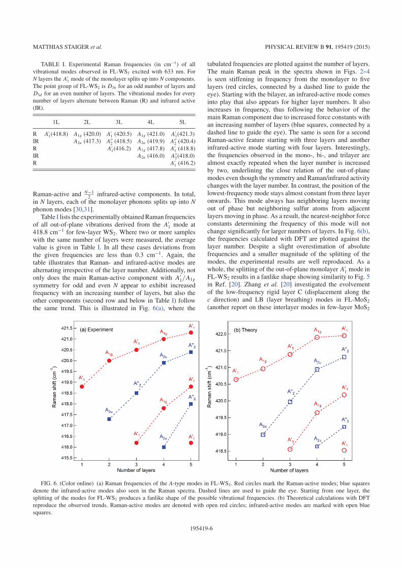
MATTHIAS STAIGER et al. PHYSICAL REVIEW B 91, 195419 (2015)
TABLE I. Experimental Raman frequencies (in cm−1) of allvibrational modes observed in FL-WS2 excited with 633 nm. ForN layers the A′
1 mode of the monolayer splits up into N components.The point group of FL-WS2 is D3h for an odd number of layers andD3d for an even number of layers. The vibrational modes for everynumber of layers alternate between Raman (R) and infrared active(IR).
1L 2L 3L 4L 5L
R A′1(418.8) A1g (420.0) A′
1 (420.5) A1g (421.0) A′1(421.3)
IR A2u (417.3) A′′2 (418.5) A2u (419.9) A′′
2 (420.4)R A′
1(416.2) A1g (417.8) A′1 (418.8)
IR A2u (416.0) A′′2(418.0)
R A′1 (416.2)
Raman-active and N−12 infrared-active components. In total,
in N layers, each of the monolayer phonons splits up into Nphonon modes [30,31].
Table I lists the experimentally obtained Raman frequenciesof all out-of-plane vibrations derived from the A′
1 mode at418.8 cm−1 for few-layer WS2. Where two or more sampleswith the same number of layers were measured, the averagevalue is given in Table I. In all these cases deviations fromthe given frequencies are less than 0.3 cm−1. Again, thetable illustrates that Raman- and infrared-active modes arealternating irrespective of the layer number. Additionally, notonly does the main Raman-active component with A′
1/A1g
symmetry for odd and even N appear to exhibit increasedfrequency with an increasing number of layers, but also theother components (second row and below in Table I) followthe same trend. This is illustrated in Fig. 6(a), where the
tabulated frequencies are plotted against the number of layers.The main Raman peak in the spectra shown in Figs. 2–4is seen stiffening in frequency from the monolayer to fivelayers (red circles, connected by a dashed line to guide theeye). Starting with the bilayer, an infrared-active mode comesinto play that also appears for higher layer numbers. It alsoincreases in frequency, thus following the behavior of themain Raman component due to increased force constants withan increasing number of layers (blue squares, connected by adashed line to guide the eye). The same is seen for a secondRaman-active feature starting with three layers and anotherinfrared-active mode starting with four layers. Interestingly,the frequencies observed in the mono-, bi-, and trilayer arealmost exactly repeated when the layer number is increasedby two, underlining the close relation of the out-of-planemodes even though the symmetry and Raman/infrared activitychanges with the layer number. In contrast, the position of thelowest-frequency mode stays almost constant from three layeronwards. This mode always has neighboring layers movingout of phase but neighboring sulfur atoms from adjacentlayers moving in phase. As a result, the nearest-neighbor forceconstants determining the frequency of this mode will notchange significantly for larger numbers of layers. In Fig. 6(b),the frequencies calculated with DFT are plotted against thelayer number. Despite a slight overestimation of absolutefrequencies and a smaller magnitude of the splitting of themodes, the experimental results are well reproduced. As awhole, the splitting of the out-of-plane monolayer A′
1 mode inFL-WS2 results in a fanlike shape showing similarity to Fig. 5in Ref. [20]. Zhang et al. [20] investigated the evolvementof the low-frequency rigid layer C (displacement along thec direction) and LB (layer breathing) modes in FL-MoS2
(another report on these interlayer modes in few-layer MoS2
FIG. 6. (Color online) (a) Raman frequencies of the A-type modes in FL-WS2. Red circles mark the Raman-active modes; blue squaresdenote the infrared-active modes also seen in the Raman spectra. Dashed lines are used to guide the eye. Starting from one layer, thesplitting of the modes for FL-WS2 produces a fanlike shape of the possible vibrational frequencies. (b) Theoretical calculations with DFTreproduce the observed trends. Raman-active modes are denoted with open red circles; infrared-active modes are marked with open bluesquares.
195419-6

SPLITTING OF MONOLAYER OUT-OF-PLANE . . . PHYSICAL REVIEW B 91, 195419 (2015)
can be found in Ref. [34]). With the support of a simpleatomic chain model the authors found a behavior similar tothe one described here for the out-of-plane vibration in WS2.Obviously, rigid-layer vibrations appear starting only from thebilayer. Strictly speaking, the difference from all other opticalmodes in FL-TMDs is that there are, consequently, only N − 1possible vibrations (where N denotes the layer number) for therigid-layer modes (E2
2g and B2g symmetry in bulk MoS2). Ofcourse, the “N modes for N layers rule” is restored again if oneadds the acoustic modes. The acoustic E′ and A′′
2 modes ofthe monolayer are the origin of the low-frequency vibrationsin FL-TMDs and will split up into N components for N layers(among them A- and E-type modes with zero frequency).
The behavior described above should, in principle, be ob-servable in other 2H-TMDs as well. Terrones et al. [21] predictan increased splitting of the Raman-active components in theorder WSe2, MoSe2, WS2, and MoS2. What distinguishes WS2
from other prominent 2H -TMDs such as WSe2 and MoS2 isthat the bulk A1g and E1
2g modes are well separated in energyand that no second-order Raman features overlap with the A1g
mode, thus making it easier to resolve the splitting of the out-of-plane mode into Raman and infrared-active components.More importantly, measuring in resonance with the opticaltransition appears to be a necessary condition to observe thefull set of vibrational modes. There is a lack of studies onRaman spectra of other FL-2H -TMDs measured under theresonance condition; often, the corresponding excitation wave-lengths are avoided because in the monolayer case the Ramanfeatures are obscured by a strong photoluminescence signal.In FL-WS2 in particular, the characteristic shape of the out-of-plane mode in resonance Raman spectra can be used as a finger-print region to unambiguously identify the number of layers.
For WS2 measured under the resonance excitation, even inthe bulk material, the A1g out-of-plane mode is accompaniedby a small shoulder that is attributed to the silent B1u
mode [12,16,29]. It had been previously attributed to aLA(K) + T A(K) combination mode [35], but the partici-pation of two phonon modes involving acoustic phonons inthis frequency region seems unlikely, especially in light ofmore recent DFT calculations showing that nowhere in theBrillouin zone do the acoustic phonons reach values above200 cm−1 [12]. The in-phase and out-of-phase vibrationalpattern of the A1g/B1u pair in bulk WS2 finds its counterpartin the variety of in- and out-of-phase vibrations observedin FL-WS2. In WS2 nanomaterials, the B1u mode gains inRaman intensity, and its evolvement can be followed inWS2 nanomaterials under pressure [29,36], in different layerorientations in thin films [37], and in WS2 nanotubes withdifferent diameters [29,38]. In these cases, a strong resonancebehavior is observed as well, much like in FL-WS2: themodes not allowed in a first-order Raman process appearmost strongly when the excitation energy is in or close toresonance with the optical transitions. In an earlier work onWS2 nanotubes [29], we found that the curvature-inducedstrain and the resultant crystal symmetry distortion accountedfor the activation of silent modes. Here, in quasi-2D materials,the situation in the absence of curvature effects is different;strain due to substrate-sample interaction is assumed to playonly a very minor role in Raman spectroscopy on supportedFL-TMDs [20].
Instead, a closer look at the nature of the excitonic transitionleading to the resonantly enhanced Raman intensity in thespectra of FL-WS2 can provide the means to elucidate theappearance of the infrared-active components of the A′
1/A1g
Raman mode around 420 cm−1. For a 633-nm excitationwavelength, the phonons couple to the A exciton situated atthe K point of the Brillouin zone. Owing to the structural rela-tionship between strong intralayer bonding in two dimensionsand weak interlayer interaction in the third dimension, likemany properties of layered TMD systems, the wave functionsof the excitons are expected to be very anisotropic. A recentwork on the orientation of luminescent excitons in FL-MoS2,isostructural to FL-WS2, reveals them to be confined entirely inplane without significant expansion in the stacking directionof individual layers [39]. This was further substantiated byDFT calculations in the LDA that explicitly showed the wavefunction of the A exciton in multilayer MoS2 to be spread outover a large area in two dimensions but with negligible densityin neighboring layers [40]. For the resonant Raman processdiscussed here this means that even for a layer number ofmore than one, the phonon couples to an A exciton localizedprimarily in one of the layers. If the N layers in FL-WS2
are to be treated approximately as N individual monolayersfor the specific case of the A excitonic resonant Raman process,there are N Raman-allowed Raman modes to be expected inthe region of the monolayer A′
1 Raman mode with similarRaman intensities. They are still split in frequency due tointerlayer interaction. Here, all N components are identifiedin the Raman measurements presented in this paper, butthe infrared-active components, speaking from the N -layersymmetry point of view, are always weaker in intensity thanthe Raman-active components. Thus, we conclude that Ramanselection rules are at least weakened but not completelybroken. This is supported by the fact that the Raman-activecomponents gain in intensity relative to the main Ramanpeak but still appear as shoulders rather than as individualpeaks.
Far from the A excitonic resonance, the few-layer WS2
cannot be treated as N individual monolayers, and the Ramanselection rules following from the few-layer symmetry strictlyapply. This is also in agreement with recent findings on newlyobserved Raman modes in FL-MoS2 in resonance with theC exciton [31].
V. CONCLUSION
In summary, we have shown experimentally as well astheoretically that the out-of-plane A′
1 mode of the WS2
monolayer splits up in the few-layer regime into N componentsfor N layers. Despite the fact that only N
2 of them for aneven number of layers and N+1
2 for an odd number of layersare Raman active, the full set of phonon modes is observedwhen the laser excitation energy is close to the A excitonictransition energy. A possible explanation for this unusualbehavior is presented by taking into account the in-planeorientation of the A exciton wave function involved in theresonant Raman scattering process. The stiffening of the mainout-of-plane phonon mode with N is also followed by all othercomponents successively added with an increasing numberof layers. Using resonant Raman scattering measurements,
195419-7
MATTHIAS STAIGER et al. PHYSICAL REVIEW B 91, 195419 (2015)
one can conclusively identify the number of layers in aspecific sample by simply counting the number of componentsof the out-of-plane A mode. The detailed analysis of theevolvement of the A′
1 mode of monolayer WS2 presentedhere should, in principle, be applicable to (i) all otherRaman modes of (ii) all layered materials in the few-layerregime.
ACKNOWLEDGMENTS
This work was supported by the Deutsche Forschungs-gemeinschaft (DFG) in the Priority Programme SPP 1459“Graphene” and by the European Research Council (ERC)through Grant No. 259286. We thank L. Madauß for hissupport with sample preparation.
[1] M. Chhowalla, H. S. Shin, G. Eda, L.-J. Li, K. P. Loh, andH. Zhang, Nat. Chem. 5, 263 (2013).
[2] Z. Ye, T. Cao, K. O’Brien, H. Zhu, X. Yin, Y. Wang, S. G. Louie,and X. Zhang, Nature (London) 513, 214 (2014).
[3] B. Zhu, H. Zeng, J. Dai, Z. Gong, and X. Cui, Proc. Natl. Acad.Sci. USA 111, 11606 (2014).
[4] A. Ramasubramaniam, Phys. Rev. B 86, 115409 (2012).[5] Q. Wang, K. Kalantar-Zadeh, A. Kis, J. Coleman, and M. S.
Strano, Nat. Nanotechnol. 7, 699 (2012).[6] H. Wang, H. Feng, and J. Li, Small 10, 2165 (2014).[7] B. Zhu, H. Zeng, J. Dai, and X. Cui, Adv. Mater. 26, 5504
(2014).[8] A. Splendiani, L. Sun, Y. Zhang, T. Li, J. Kim, C.-Y. Chim, G.
Galli, and F. Wang, Nano Lett. 10, 1271 (2010).[9] K. F. Mak, C. Lee, J. Hone, J. Shan, and T. F. Heinz, Phys. Rev.
Lett. 105, 136805 (2010).[10] P. Tonndorf, R. Schmidt, P. Bottger, X. Zhang, J. Borner, A.
Liebig, M. Albrecht, C. Kloc, O. Gordan, D. R. T. Zahn, S. M.de Vasconcellos, and R. Bratschitsch, Opt. Express 21, 4908(2013).
[11] H. S. S. R. Matte, A. Gomathi, A. K. Manna, D. J. Late, R.Datta, S. K. Pati, and C. N. R. Rao, Angew. Chem. Int. Ed. 122,4153 (2010).
[12] A. Molina-Sanchez and L. Wirtz, Phys. Rev. B 84, 155413(2011).
[13] M. Thripuranthaka and J. Dattatray, ACS Appl. Mater. Interfaces6, 1158 (2014).
[14] A. A. Mitioglu, P. Plochocka, G. Deligeorgis, S. Anghel,L. Kulyuk, and D. K. Maude, Phys. Rev. B 89, 245442 (2014).
[15] T. Wieting and J. Verble, Phys. Rev. B 3, 4286 (1971).[16] C. Sourisseau, M. Fouassier, M. Alba, A. Ghorayeb, and
O. Gorochov, Mater. Sci. Eng. B 3, 119 (1989).[17] C. Lee, H. Yan, L. E. Brus, T. F. Heinz, J. Hone, and S. Ryu,
ACS Nano 4, 2695 (2010).[18] G. Plechinger, S. Heydrich, J. Eroms, D. Weiss, C. Schuller, and
T. Korn, Appl. Phys. Lett. 101, 101906 (2012).[19] A. Berkdemir, H. R. Gutierrez, A. R. Botello-Mendez, N. Perea-
Lopez, A. L. Elıas, C.-I. Chia, B. Wang, V. H. Crespi, F. Lopez-Urıas, J.-C. Charlier, H. Terrones, and M. Terrones, Sci. Rep. 3,1755 (2013).
[20] X. Zhang, W. P. Han, J. B. Wu, S. Milana, Y. Lu, Q. Q. Li,A. C. Ferrari, and P. H. Tan, Phys. Rev. B 87, 115413 (2013).
[21] H. Terrones, E. Del Corro, S. Feng, J. M. Poumirol, D. Rhodes,D. Smirnov, N. R. Pradhan, Z. Lin, M. A. T. Nguyen, A. L. Elıas,
T. E. Mallouk, L. Balicas, M. A. Pimenta, and M. Terrones,Sci. Rep. 4, 4215 (2014).
[22] J. Wilson and A. Yoffe, Adv. Phys. 18, 193 (1969).[23] S. J. Clark, M. D. Segall, C. J. Pickard, P. J. Hasnip, M. J. Probert,
K. Refson, and M. Payne, Z. Kristallogr. 220, 567 (2005).[24] W. Schutte, J. D. Boer, and F. Jellinek, J. Solid. State Chem. 70,
207 (1987).[25] J. Verble and T. Wieting, Phys. Rev. Lett. 25, 362 (1970).[26] W. Zhao, Z. Ghorannevis, K. K. Amara, J. R. Pang, M. Toh,
X. Zhang, C. Kloc, P. H. Tane, and G. Eda, Nanoscale 5, 9677(2013).
[27] D. Late, B. Liu, H. Matte, C. Rao, and V. Dravid, Adv. Funct.Mater. 22, 1894 (2012).
[28] M. Yamamoto, S. T. Wang, M. Ni, Y.-F. Lin, S.-L. Li, S. Aikawa,W.-B. Jian, K. Ueno, K. Wakabayashi, and K. Tsukagoshi, ACSNano 8, 3895 (2014).
[29] M. Staiger, P. Rafailov, K. Gartsman, H. Telg, M. Krause,G. Radovsky, A. Zak, and C. Thomsen, Phys. Rev. B 86, 165423(2012).
[30] X. Luo, Y. Zhao, J. Zhang, Q. Xiong, and S. Y. Quek, Phys. Rev.B 88, 075320 (2013).
[31] N. Scheuschner, R. Gillen, M. Staiger, and J. Maultzsch, Phys.Rev. B (to be published).
[32] N. Scheuschner, O. Ochedowski, M. Schleberger, andJ. Maultzsch, Phys. Status Solidi B 249, 2644 (2012).
[33] H. Li, Q. Zhang, C. C. R. Yap, B. K. Tay, T. H. T. Edwin,A. Olivier, and D. Baillargeat, Adv. Funct. Mater. 22, 1385(2012).
[34] H. Zeng, B. Zhu, K. Liu, J. Fan, X. Cui, and Q. M. Zhan, Phys.Rev. B 86, 241301(R) (2012).
[35] C. Sourisseau, F. Cruege, M. Fouassier, and M. Alba, Chem.Phys. 150, 281 (1991).
[36] S. D. Yu, L. X. Chang, H. B. Yang, B. B. Liu, Y. Y. Hou, L.Wang, M. G. Yao, T. Cui, and G. T. Zou, J. Phys. Condens.Matter 19, 425228 (2007).
[37] J. Chung, Z. Dai, K. Adib, and F. Ohuchi, Thin Solid Films 335,106 (1998).
[38] M. Krause, M. Virsek, M. Remskar, N. Salacan, N. Fleischer,L. Chen, P. Hatto, A. Kolitsch, and W. Moller, ChemPhysChem10, 2221 (2009).
[39] J. A. Schuller, S. Karaveli, T. Schiros, K. He, S. Yang, I.Kymissis, J. Shan, and R. Zia, Nat. Nanotechnol. 8, 271 (2013).
[40] A. Molina-Sanchez, D. Sangalli, K. Hummer, A. Marini, andL. Wirtz, Phys. Rev. B 88, 045412 (2013).
195419-8

B. Papers as published
B.3. Physical Review B 94, 035430 (2016)
78

PHYSICAL REVIEW B 94, 035430 (2016)
Raman spectroscopy of intercalated and misfit layer nanotubes
Matthias Staiger,1,* Vladimir Bacic,2 Roland Gillen,1 Gal Radovsky,3 Konstantin Gartsman,4 Reshef Tenne,3 Thomas Heine,2,5
Janina Maultzsch,1 and Christian Thomsen1
1Institut fur Festkorperphysik, Technische Universitat Berlin, Hardenbergstr. 36, 10623 Berlin, Germany2Department of Physics and Earth Sciences, Jacobs University Bremen gGmbH Campus Ring 1, 28759 Bremen, Germany
3Department of Materials and Interfaces, Weizmann Institute of Science, Rehovot 76100, Israel4Electron Microscopy Unit, Weizmann Institute of Science, Rehovot 76100, Israel
5Wilhelm-Ostwald-Institut fur Physikalische und Theoretische Chemie, Linnestr. 2, 04103 Leipzig, Germany(Received 12 January 2016; revised manuscript received 23 June 2016; published 18 July 2016)
We present Raman spectra of misfit layer (PbS)1.14NbS2 nanotubes and lead intercalated NbS2 nanotubes.They represent interesting model systems to investigate the nature of interlayer interaction in layered materials.A direct correlation to the Raman modes of the parent 2H -NbS2 compound exists, but some modes are seendrastically upshifted in frequency in the misfit layer and intercalated compound while others remain almostunchanged. On the basis of the Raman spectroscopic investigations and with the help of supporting calculationswe examine different interlayer bonding mechanisms and contribute to the discussion as to why these frequencyshifts occur.
DOI: 10.1103/PhysRevB.94.035430
I. INTRODUCTION
In recent years transition metal dichalcogenide nanostruc-tures (TMDCs) attracted a lot of interest. TMDCs span a widevariety of structures and physical properties, ranging fromisolators to semiconductors, metals, and superconductors.Like for carbon based compounds, dimensionality is animportant factor determining the properties of TMDCs. Apartfrom mono- and few-layer quasi-two-dimensional structuresa number of TMDC nanotubes has been successfully synthe-sized [1]. Recently, there were first reports on the synthesisand characterization of nanotubes consisting of alternatinglayers of SnS/PbS and SnS2/NbS2 rolled up so as to reducethe lattice mismatch between the two materials [2–4]. Thesenanotubes belong to the family of misfit layer compounds(MLCs) composed of transition metal dichalcogenides T X2
(T = Ti, V, Cr, Nb, Ta and the main group metal Sn; X = S,Se) and layers MX and RX (M = Sn, Pb, Sb, Bi, R = rareearth metals).
In their bulk form MLCs have been investigated fordecades [5–8], and research has made evident that the pos-sibility of combining these very different classes of materialsmakes for a plethora of structures and physical properties.They all have in common that they crystallize in highly orderedanisotropic structures, as will be detailed below. Consequently,research has always been accompanied by the question asto why these structures are so remarkably stable. A diverseset of methods ranging from (angle-resolved) photoelectronspectroscopy [9,10], electron microprobe analysis [11], pho-toemission microspectroscopy [12], bond valence [13] andab initio density functional calculations [14], and not leastRaman spectroscopy [15–19] have all been dedicated to gaininsight into the nature of interlayer interaction governing theoverall stability of MLCs. Apart from the intrinsic importanceof MLCs as a model system for studying interlayer interactionand how intercalation can change the electronic properties
*Corresponding author: [email protected]
of the host structure in layered systems, MLCs exhibit inter-esting thermoelectric properties [20–23], and many of themare superconductors [24]. With current research on layeredmaterials increasingly focusing on low-dimensional systems,an ever growing family of tubular misfit layer compoundshas been recently synthesized [2–4,25–27], but studies ontheir electronic and optical properties are as yet scarce [28].In this context the present study aims to revisit studies onthe properties of bulk MLCs and apply the findings to theirnanostructured counterparts. Here, Raman spectroscopy hasbeen the method of choice as it not only uncovers thevibrational properties but provides information about theelectronic structure of the investigated materials. As such, thisstudy contributes to the deciphering of the nature of interlayerinteraction in tubular misfit layer nanostructures. The focuslies on representatives of a larger family of nanotubes,(PbS)1.14-NbS2 and Pb-intercalated NbS2 nanotubes, whereboth components are low temperature superconductors [29].
Structurally similar to their bulk counterparts, in the rolledup T X2 layers, transition metal atoms are sandwiched betweensix chalcogenide atoms whereas the MX and RX layerscommonly adopt a distorted rock salt structure. The layersare stacked along the c axis. With a few exceptions, the layersshare a common b axis length. The a axes are incommensuratemeaning that the ratio of the two a sublattice constants isirrational. This affects the stoichiometry of the overall systemwhich is expressed by the index x in (MX)xT X2.
In (PbS)1.14NbS2, a two atoms thick part of the PbS bulkstructure is cut out to form a planar composite structurealternating with NbS2 layers. The cubic symmetry of thelead sulfide layer is broken in the misfit layer compoundwith the Pb atoms protruding into the van der Waals gapbetween the layered subsystems. Electronically, bulk PbS isa narrow-gap semiconductor (Egap = 0.42 eV [30]). NbS2
crystallizes in trigonal prismatic coordination, where theNb atom is placed between six sulfur atoms forming twotetrahedrons. In contrast to other 2H -dichalcogenides likeMoS2 and WS2, which exhibit a transition from an indirect to adirect band gap material once the thickness has been reduced to
2469-9950/2016/94(3)/035430(10) 035430-1 ©2016 American Physical Society

MATTHIAS STAIGER et al. PHYSICAL REVIEW B 94, 035430 (2016)
aNbS2
aPbS
(a)
(b)
(c) (d)
CF
cb
ca
c
CF
b
- Pb
- S
- Nb
FIG. 1. (a) Structure of the misfit layer compound (PbS)1.14NbS2
in the a-b plane. The ratio of the a axes is irrational, thereforethe compounds are classified as misfit layer compounds (MLC).(b) and (c): The structure of the misfit compound viewed along thecommensurate b and the incommensurate a direction, respectively.(d) View along the normal to the (11.0) plane according to the pseudo-hexagonal system of labeling of the NbS2 material intercalated withlead atoms in linear coordination to neighboring S atoms (ICSD col.code. 74698).
a monolayer, NbS2 stays a metal even in the two-dimensionallimit [31]. The metal character stems from a partially filled4dz2 Nb orbital around the Fermi energy. In the misfit layercompound (MLC) the NbS2 layers remain fairly rigid andalmost preserve the structure of the pristine 2H -NbS2 [14].Figure 1(a) shows a view on the a-b plane of the (PbS)1.14NbS2
compound. In the simple orthorhombic conventional unit cell,the sublattices share a common b lattice constant, but thea lattice constants stay incommensurate with a lattice ratioof aPbS/aNbS2 ≈ √
3 which makes for 4aPbS ≈ 7aNbS2 [32].In Figs. 1(b) and 1(c) a view along the two in-plane latticedirections is depicted. Along the c direction, the CF stackingsequence is common in bulk (PbS)1.14NbS2 [7], but loses itsvalidity in the misfit nanotubes. The conventional unit cell
contains 28 units of NbS2 and 32 units of PbS, which makes forthe index of 1.14. Between the layers, besides the van der Waalsinteraction, some coordinative bonding may exist. In misfitlayer compounds, the MX material is often characterized asthe intercalant in between the T X2 layers.
This is also the case in the second type of nanotubesinvestigated in this study, Pb-NbS2 nanotubes, where thelead undoubtedly can be described as an intercalant. Here,the Pb atoms are, rather unusually, linearly coordinated totwo S atoms of the adjacent NbS2 slabs, as can be seen inFig. 1(d). Thus in the c direction not the metal atoms but theS atoms are found on top of each other [4,33]. The expectedatomic ratio of 1:1 between the niobium and the lead atomswas confirmed previously in Ref. [34]. Strictly speaking, thePb-NbS2 nanotubes are thus not misfit layer compounds but,as we will see, the intercalants have strikingly similar effecton the Raman spectra of the host NbS2 layer as the lead sulfidelayers in the MLC.
In this paper we present Raman spectra of (PbS)1.14NbS2
nanotubes and NbS2 nanotubes intercalated with lead. Whilethe vibrational properties of the former can be compared toits parent material, the latter has not been investigated before.Our focus lies on the changes in the Raman frequencies of themisfit layer and intercalated materials compared to the pristinecompound. The different mechanisms of interlayer bondingare critically discussed on the basis of the results of the Ramanspectroscopic investigation. The popular charge transfer hy-pothesis is challenged experimentally as well as theoretically,and we propose an alternative way to explain the drastic Ramanfrequency upshifts observed in both compounds.
A. Experiment
Pb-Nb-S tubular structures were synthesized via chemicalvapor transport technique in evacuated quartz ampules as wasdescribed in Ref. [4]. Reference [4] also describes in detail thecharacterization process. Prior to Raman measurements (highresolution) TEM images were taken of each nanotube andthe respective type was identified by determining the layerperiodicities. In Fig. 2(a) this can be seen for a Pb-NbS2
nanotube with 0.88 nm periodicity (NbS2 layer and atomic Pblayers are alternating). The same is shown for a (PbS)1.14NbS2
misfit layer nanotube in Fig. 2(b). Here, PbS and NbS2 layersare alternating, resulting in a 1.20 nm periodicity. Additionally,energy-dispersive x-ray (EDS) spectra and selected areaelectron diffraction (SAED) patterns were at hand and aredescribed in Ref. [4]. Raman spectra of individual misfitlayer nanotubes were recorded in backscattering geometryemploying a frequency doubled Nd:YAG laser emitting at532 nm. The scattered light was analyzed using a LabRamHR spectrometer with a 600/mm grating and a Peltier-cooled charge-coupled device. The spectral resolution wasapproximately 2 cm−1. Laser power had to be limited to130 μW so as to avoid burning the underlying thin carbon TEMsubstrate. Due to the investigated materials being rather poorRaman scatterers, accumulation times exceeded 20 minutes inmost cases and several spectra recorded at the same positionof the sample had to be summed to get appreciable signal.
Density functional theory (DFT) calculations were carriedout using the local-density approximation (LDA), with
035430-2

RAMAN SPECTROSCOPY OF INTERCALATED AND MISFIT . . . PHYSICAL REVIEW B 94, 035430 (2016)
FIG. 2. Structural characterization of the nanotubes. (a) High and low (inset) TEM images of a Pb-NbS2 nanotube investigated in thispaper. The layer periodicity of 0.88 nm (alternating layers of Pb atoms and NbS2) can be identified in a line profile (inset) of the nanotube areaenclosed by the rectangle. (b) High and low (inset) TEM images of a (PbS)1.14NbS2 misfit layer nanotube investigated in this paper. The lineprofile (inset) taken from the area enclosed by the rectangle depicts the layer periodicity of 1.20 nm corresponding to alternating layers of PbSand NbS2.
plane-wave basis and the projector-augmented wave (PAW)method, as implemented in the Quantum ESPRESSO (QE)package [35]. The Brillouin zone (BZ) was sampled usinga 24 × 24 × 6 Monkhorst-pack (MP) grid for NbS2 andPb-NbS2, and a 3 × 12 × 3 MP grid for (PbS)1.14NbS2.The cutoffs for plane-wave and charge-density expansionwere set to 65 Ry and 650 Ry, respectively. Thresholdfor structural optimization was set to 2 (meV/A)/atom inall three structures. Phonon frequencies were calculatedusing the linear-response (DFPT) technique, again withinthe QE package. To obtain the entire phonon dispersion inthe case of NbS2 and Pb-NbS2, dynamical matrices werecalculated on a 6 × 6 × 1 MP grid in the BZ. Although themeasurements were done on nanotubes, in the calculations athree-dimensional system, with the unit cells given in Fig. 1,was assumed. Since the studied nanotubes are �100 nm indiameter and the number of walls are well above ten in allcases studied, this is assumed to be a good approximation.
B. Results
Raman spectra of 2H -NbS2 were obtained by Nakashimaet al. [36] thirty years ago. The two main Raman modeswere observed at 379 cm−1 (A1g) and 309 cm−1 (E1
2g). Inthe regular (PbS)1.14NbS2 nanotubes, PbS and NbS2 wallsare alternating [4]. Coming from the bulk 2H -NbS2 D4
6h
structure, the symmetry of the NbS2 part is at least reducedto the monolayer D3h structure; additional distortion mightoccur due to charge transfer, covalent interlayer bonding, andnanotube curvature. However, in this paper, Raman modeassignments are based on the D3h structure for simplicity.
Due to the lack of a center of inversion, the bulk A1g and B1u
modes reduce to A′1 symmetry, and the E1
2g and E1u modesbecome in-plane E′ modes. In backscattering geometry, the E′′mode (E1g and E2u in the bulk) is Raman forbidden. In total,the irreducible representations of the phonon modes in thesymmetry group D3h at the � point of the hexagonal Brillouinzone are � = A′
1 + E′′ + 2A′′2 + 2E′.
From the bulk PbS structure, a two atoms thick part iscut out to form the PbS walls. They are significantly distortedcompared to the NaCl type parent material with the lead atomsalways protruding into the van der Waals gap. In contrast tothe three-dimensional bonding network of bulk PbS, first-orderRaman scattering becomes allowed [15].
Figure 3(a) shows Raman spectra of (PbS)1.14NbS2nanotubes. Two regions can be singled out: below 200 cm−1
with Raman modes that have been attributed to the PbS layersin the literature [15,18,37] and above 340 cm−1, where thetwo main peaks can be identified as the E′ and A′
1 mode of theNbS2 layer [15,38]. The A′
1 mode is situated at ∼378 cm−1
and thus only very weakly downshifted with respect tothe A1g mode of bulk NbS2. A drastic change in Ramanfrequency on the other hand is observed for the E′ modethat is upshifted by more than 40 wave numbers comparedto the E2g mode of bulk NbS2 and lies at ∼353 cm−1. Theupshift is up to 12 wave numbers stronger than that found inbulk (PbS)1.14NbS2 [15,18,37,38]. Possible reasons for thisrather unusual behavior, such as charge transfer from theMX to the T X2 layer, strain effects, interlayer bonding, andthe monolayer nature of the T X2 part, will be discussed indetail in the next section. Typical full widths at half maximum(FWHMs) of the E′ and A′
1 mode are 13 cm−1 and 15 cm−1,respectively. Surprisingly, the relative intensities of the two
035430-3
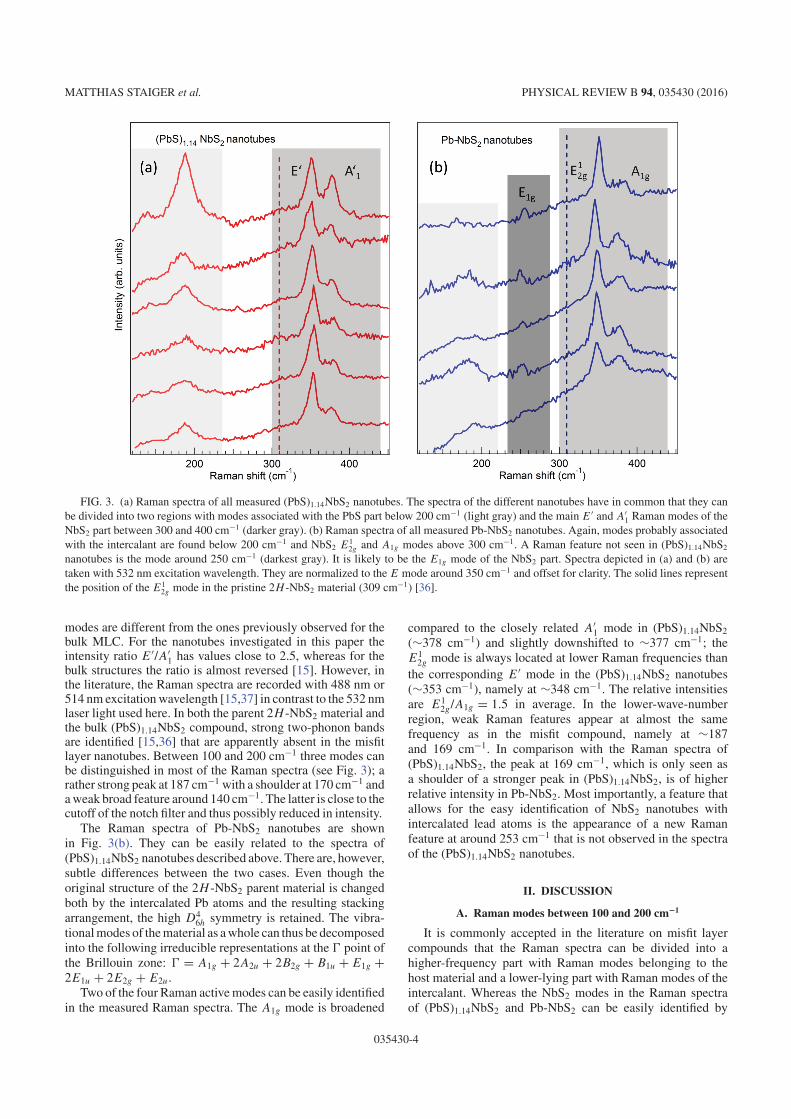
MATTHIAS STAIGER et al. PHYSICAL REVIEW B 94, 035430 (2016)
FIG. 3. (a) Raman spectra of all measured (PbS)1.14NbS2 nanotubes. The spectra of the different nanotubes have in common that they canbe divided into two regions with modes associated with the PbS part below 200 cm−1 (light gray) and the main E′ and A′
1 Raman modes of theNbS2 part between 300 and 400 cm−1 (darker gray). (b) Raman spectra of all measured Pb-NbS2 nanotubes. Again, modes probably associatedwith the intercalant are found below 200 cm−1 and NbS2 E1
2g and A1g modes above 300 cm−1. A Raman feature not seen in (PbS)1.14NbS2
nanotubes is the mode around 250 cm−1 (darkest gray). It is likely to be the E1g mode of the NbS2 part. Spectra depicted in (a) and (b) aretaken with 532 nm excitation wavelength. They are normalized to the E mode around 350 cm−1 and offset for clarity. The solid lines representthe position of the E1
2g mode in the pristine 2H -NbS2 material (309 cm−1) [36].
modes are different from the ones previously observed for thebulk MLC. For the nanotubes investigated in this paper theintensity ratio E′/A′
1 has values close to 2.5, whereas for thebulk structures the ratio is almost reversed [15]. However, inthe literature, the Raman spectra are recorded with 488 nm or514 nm excitation wavelength [15,37] in contrast to the 532 nmlaser light used here. In both the parent 2H -NbS2 material andthe bulk (PbS)1.14NbS2 compound, strong two-phonon bandsare identified [15,36] that are apparently absent in the misfitlayer nanotubes. Between 100 and 200 cm−1 three modes canbe distinguished in most of the Raman spectra (see Fig. 3); arather strong peak at 187 cm−1 with a shoulder at 170 cm−1 anda weak broad feature around 140 cm−1. The latter is close to thecutoff of the notch filter and thus possibly reduced in intensity.
The Raman spectra of Pb-NbS2 nanotubes are shownin Fig. 3(b). They can be easily related to the spectra of(PbS)1.14NbS2 nanotubes described above. There are, however,subtle differences between the two cases. Even though theoriginal structure of the 2H -NbS2 parent material is changedboth by the intercalated Pb atoms and the resulting stackingarrangement, the high D4
6h symmetry is retained. The vibra-tional modes of the material as a whole can thus be decomposedinto the following irreducible representations at the � point ofthe Brillouin zone: � = A1g + 2A2u + 2B2g + B1u + E1g +2E1u + 2E2g + E2u.
Two of the four Raman active modes can be easily identifiedin the measured Raman spectra. The A1g mode is broadened
compared to the closely related A′1 mode in (PbS)1.14NbS2
(∼378 cm−1) and slightly downshifted to ∼377 cm−1; theE1
2g mode is always located at lower Raman frequencies thanthe corresponding E′ mode in the (PbS)1.14NbS2 nanotubes(∼353 cm−1), namely at ∼348 cm−1. The relative intensitiesare E1
2g/A1g = 1.5 in average. In the lower-wave-numberregion, weak Raman features appear at almost the samefrequency as in the misfit compound, namely at ∼187and 169 cm−1. In comparison with the Raman spectra of(PbS)1.14NbS2, the peak at 169 cm−1, which is only seen asa shoulder of a stronger peak in (PbS)1.14NbS2, is of higherrelative intensity in Pb-NbS2. Most importantly, a feature thatallows for the easy identification of NbS2 nanotubes withintercalated lead atoms is the appearance of a new Ramanfeature at around 253 cm−1 that is not observed in the spectraof the (PbS)1.14NbS2 nanotubes.
II. DISCUSSION
A. Raman modes between 100 and 200 cm−1
It is commonly accepted in the literature on misfit layercompounds that the Raman spectra can be divided into ahigher-frequency part with Raman modes belonging to thehost material and a lower-lying part with Raman modes of theintercalant. Whereas the NbS2 modes in the Raman spectraof (PbS)1.14NbS2 and Pb-NbS2 can be easily identified by
035430-4

RAMAN SPECTROSCOPY OF INTERCALATED AND MISFIT . . . PHYSICAL REVIEW B 94, 035430 (2016)
comparison with the bulk parent material, this cannot besaid about the MX part of the structure. First-order Ramanscattering is not allowed for the original three-dimensionalbulk PbS structure but becomes possible in the distorteddouble-layer structure of PbS in (PbS)1.14NbS2. In principle,three sources for the Raman features between 100 and200 cm−1 are conceivable in the MLC: (i) phonons stemmingfrom the PbS part of the MLC, (ii) second-order modes andtwo-phonon density of states, or (iii) defect, disorder-inducedmodes.
(i) The main peak at 189 cm−1 in the Raman spectra of theMLC nanotubes is observed in the Raman spectra of the bulkMLC as well [15,18,37] and has been identified as one of twoPbS modes of A type symmetry. By comparison with a workby Kisoda et al. [17] on misfit layer compounds of 2H -TaS2
it is likely to be the symmetric layer breathing mode of PbS;the frequency of the other A type mode of PbS was reported tobe around 80 cm−1 [15], too low-lying to be observed in thispaper. As a rather surprising result, the mode at 189 cm−1 thatcould be related to PbS still occurs in the spectra of Pb-NbS2
nanotubes (albeit with only weak Raman intensity), despitethe assumption that no lead sulfide layers are present in thestructure. This raises the question whether there are “pockets”of PbS still present in the structure of the Pb-NbS2 nanotubesthat result in PbS modes depending on the local environment.This would also explain the different intensities observed fordifferent Pb-NbS2 nanotubes. Another idea would be that anearly covalent bonding of Pb atoms to the neighboring NbS2
layers could give rise to a PbS-like phonon density of states.(ii) The peak at 189 cm−1 is rather broad, which is unusual
for a first order Raman mode but typical for a two-phonon band.Very broad two-phonon bands appear in the spectra of bulk2H -NbS2 at higher wave numbers between 200–300 cm−1 [36]
and are unlikely to be accountable for the features just below200 cm−1 in the MLC. It seems possible that second ordermodes of the intercalant appear in the spectra of the MLCas well as in Pb-NbS2. The phonon dispersion of Pb-NbS2 isshown in Fig. 4(b); for comparison the phonon dispersion ofthe parent 2H -NbS2 is depicted in Fig. 4(a). At the � pointone can see the two first order Pb-NbS2 modes at 364 and388 cm−1, but there are also lower-lying modes at 66, 98,and 103 cm−1. The atomic displacement patterns (not shown)reveal for the second of these modes that the Pb atoms andNbS2 vibrate against each other as rigid layers; for the thirdmode NbS2 layers perform breathinglike motions while thePb layer is not vibrating. Second-order scattering of both ofthese modes could in principle be responsible for the Ramanfeatures seen at 189 and 170 cm−1 in Pb-NbS2. The questionthen arises if similar patterns would be observable in the misfitlayer compound with the PbS layer playing the role of theintercalant atoms in Pb-NbS2.
(iii) Raman spectra of the 3R-NbS2 polytype exhibit a broadphonon band centered around 160 cm−1 [36,39]. McMullanet al. [39] attribute it to an impurity or defect mode possibly re-sulting from the expected nonstoichiometry of 3R-NbS2 withsome extra Nb atoms located in the van der Waals gap [40]. Onemight argue that the situation here is similar. Both 3R-NbS2
and Pb-NbS2 as well as the misfit layer compound havedifferent stacking orders compared to 2H -NbS2, and all threeof the compounds exhibit a strong upshift of the E1
2g modecompared to 2H -NbS2. As we will discuss later, there isstrong likelihood of metal cross substitution in the misfit layercompound [12]. The exchange of Pb atoms in the PbS layerwith Nb atoms of the NbS2 layer and vice versa could indeedlead to an impurity-induced Raman mode in the spectra of the(PbS)1.14NbS2 nanotubes. The feature at around 140 cm−1
Γ Γ Γ ΓM MK K
2H-NbS2
Pb-NbS2
E1g
A1g
E2g1
0
50
100
150
200
250
300
350
400
450
0
50
100
150
200
250
300
350
400
450(a) (b)
ν(c
m-1
)
FIG. 4. (a) Phonon dispersion of the parent 2H -NbS2 bulk material. Above 200 cm−1 at the � point, three first order Raman modes, the E1g ,E1
2g , and A1g mode, are marked with blue circles and their calculated frequencies are listed in Table I. (b) The main features of the dispersionare reproduced in the dispersion of lead intercalated NbS2. The three main �-point Raman modes are seen above 250 cm−1, with the two E
type modes considerably upshifted compared to their frequency in NbS2. The frequency of the A1g mode, on the other hand, stays nearly thesame. Modes with contributions from the intercalant lead atoms are found around 100 cm−1.
035430-5
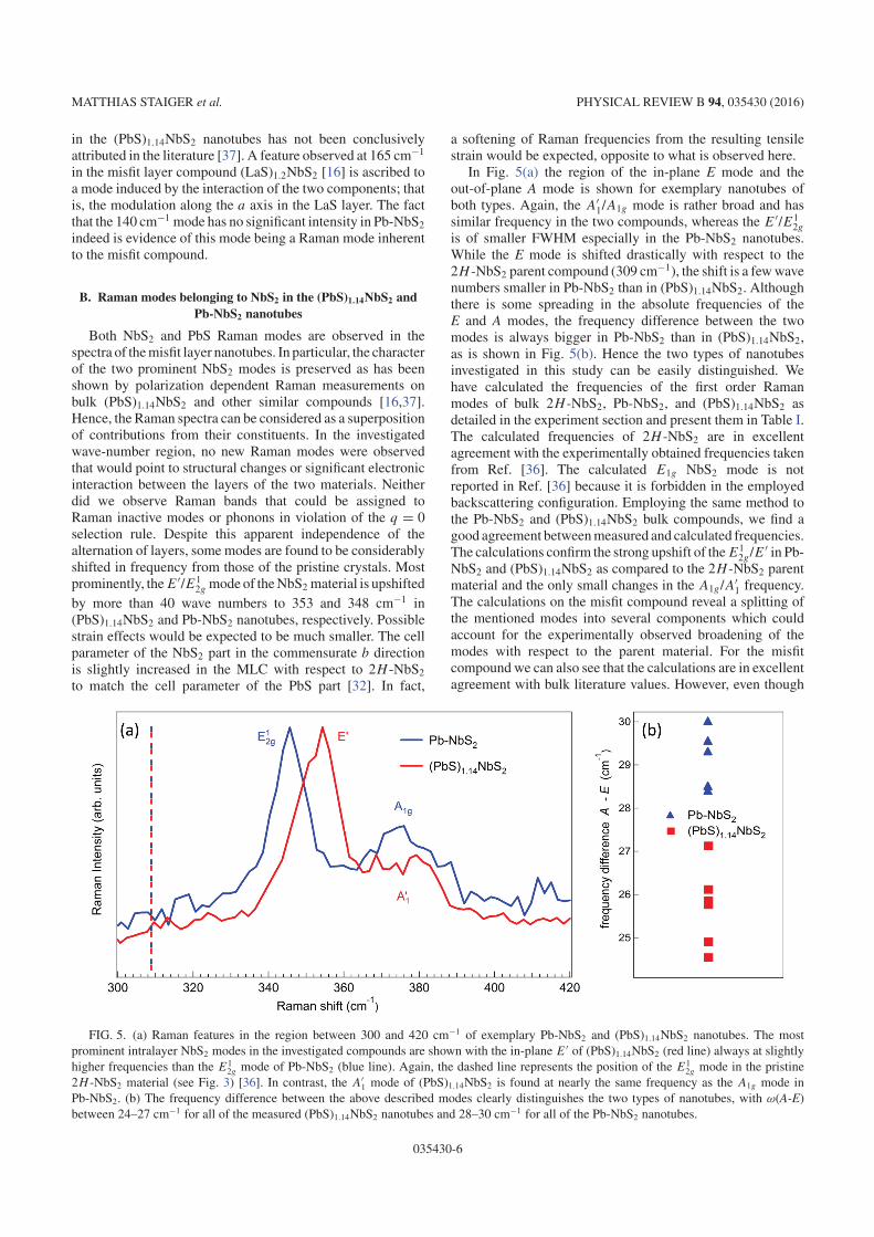
MATTHIAS STAIGER et al. PHYSICAL REVIEW B 94, 035430 (2016)
in the (PbS)1.14NbS2 nanotubes has not been conclusivelyattributed in the literature [37]. A feature observed at 165 cm−1
in the misfit layer compound (LaS)1.2NbS2 [16] is ascribed toa mode induced by the interaction of the two components; thatis, the modulation along the a axis in the LaS layer. The factthat the 140 cm−1 mode has no significant intensity in Pb-NbS2
indeed is evidence of this mode being a Raman mode inherentto the misfit compound.
B. Raman modes belonging to NbS2 in the (PbS)1.14NbS2 andPb-NbS2 nanotubes
Both NbS2 and PbS Raman modes are observed in thespectra of the misfit layer nanotubes. In particular, the characterof the two prominent NbS2 modes is preserved as has beenshown by polarization dependent Raman measurements onbulk (PbS)1.14NbS2 and other similar compounds [16,37].Hence, the Raman spectra can be considered as a superpositionof contributions from their constituents. In the investigatedwave-number region, no new Raman modes were observedthat would point to structural changes or significant electronicinteraction between the layers of the two materials. Neitherdid we observe Raman bands that could be assigned toRaman inactive modes or phonons in violation of the q = 0selection rule. Despite this apparent independence of thealternation of layers, some modes are found to be considerablyshifted in frequency from those of the pristine crystals. Mostprominently, the E′/E1
2g mode of the NbS2 material is upshiftedby more than 40 wave numbers to 353 and 348 cm−1 in(PbS)1.14NbS2 and Pb-NbS2 nanotubes, respectively. Possiblestrain effects would be expected to be much smaller. The cellparameter of the NbS2 part in the commensurate b directionis slightly increased in the MLC with respect to 2H -NbS2
to match the cell parameter of the PbS part [32]. In fact,
a softening of Raman frequencies from the resulting tensilestrain would be expected, opposite to what is observed here.
In Fig. 5(a) the region of the in-plane E mode and theout-of-plane A mode is shown for exemplary nanotubes ofboth types. Again, the A′
1/A1g mode is rather broad and hassimilar frequency in the two compounds, whereas the E′/E1
2g
is of smaller FWHM especially in the Pb-NbS2 nanotubes.While the E mode is shifted drastically with respect to the2H -NbS2 parent compound (309 cm−1), the shift is a few wavenumbers smaller in Pb-NbS2 than in (PbS)1.14NbS2. Althoughthere is some spreading in the absolute frequencies of theE and A modes, the frequency difference between the twomodes is always bigger in Pb-NbS2 than in (PbS)1.14NbS2,as is shown in Fig. 5(b). Hence the two types of nanotubesinvestigated in this study can be easily distinguished. Wehave calculated the frequencies of the first order Ramanmodes of bulk 2H -NbS2, Pb-NbS2, and (PbS)1.14NbS2 asdetailed in the experiment section and present them in Table I.The calculated frequencies of 2H -NbS2 are in excellentagreement with the experimentally obtained frequencies takenfrom Ref. [36]. The calculated E1g NbS2 mode is notreported in Ref. [36] because it is forbidden in the employedbackscattering configuration. Employing the same method tothe Pb-NbS2 and (PbS)1.14NbS2 bulk compounds, we find agood agreement between measured and calculated frequencies.The calculations confirm the strong upshift of the E1
2g /E′ in Pb-NbS2 and (PbS)1.14NbS2 as compared to the 2H -NbS2 parentmaterial and the only small changes in the A1g/A′
1 frequency.The calculations on the misfit compound reveal a splitting ofthe mentioned modes into several components which couldaccount for the experimentally observed broadening of themodes with respect to the parent material. For the misfitcompound we can also see that the calculations are in excellentagreement with bulk literature values. However, even though
FIG. 5. (a) Raman features in the region between 300 and 420 cm−1 of exemplary Pb-NbS2 and (PbS)1.14NbS2 nanotubes. The mostprominent intralayer NbS2 modes in the investigated compounds are shown with the in-plane E′ of (PbS)1.14NbS2 (red line) always at slightlyhigher frequencies than the E1
2g mode of Pb-NbS2 (blue line). Again, the dashed line represents the position of the E12g mode in the pristine
2H -NbS2 material (see Fig. 3) [36]. In contrast, the A′1 mode of (PbS)1.14NbS2 is found at nearly the same frequency as the A1g mode in
Pb-NbS2. (b) The frequency difference between the above described modes clearly distinguishes the two types of nanotubes, with ω(A-E)between 24–27 cm−1 for all of the measured (PbS)1.14NbS2 nanotubes and 28–30 cm−1 for all of the Pb-NbS2 nanotubes.
035430-6

RAMAN SPECTROSCOPY OF INTERCALATED AND MISFIT . . . PHYSICAL REVIEW B 94, 035430 (2016)
TABLE I. Calculated and experimentally obtained Raman frequencies (in cm−1) of the bulk 2H -NbS2 structure, the lead intercalated NbS2
material, and the misfit layer (PbS)1.14NbS2 compound. Where available, literature bulk values are added. The in-plane E modes shift up infrequency from the parent material to Pb-NbS2 and (PbS)1.14NbS2, whereas the out-of-plane A mode remains almost constant.
D46h 2H-NbS2 2H-NbS2 Pb-NbS2 Pb-NbS2 D3h (PbS)1.14NbS2 (PbS)1.14NbS2 (PbS)1.14NbS2
symm. bulk calc. bulk exp. [36] bulk calc. NT exp. symm. bulk calc. bulk exp. [37] NT exp.
E1g 217 260 253 E′′ 237, 241E1
2g 306 309 364 348 E′ 333-340 342 353A1g 383 380 388 377 A′
1 372-379 375 378
the nanotubes investigated in this paper are hundreds ofnanometers in diameter, have a large number of walls, andthus can be considered as bulklike, the measured Ramanfrequencies in the nanotube deviate somewhat from the bulkvalues. This is even more so for the intercalated Pb-NbS2
nanotubes. There is no literature on the Raman spectrum of thePb-NbS2 bulk, but bulk calculations and measured nanotubefrequencies differ more strongly than in the calculated andmeasured MLCs. The calculations also show that the E1
2g/E′mode is not the only mode exhibiting an upshift but thatsimilar frequency shifts can be expected for the E1g mode of2H -NbS2 in the intercalated and the misfit compounds. Thisis in disagreement with Ref. [39], where the authors identify aRaman feature in 2H -NbS2 around 260 cm−1 as the E1g mode,although they describe their assignment as somewhat tentativeas it deviates strongly from their calculated 2H -NbS2 phononfrequencies. On the other hand, the Raman mode observed at258 cm−1 in the stage-2 MLC (LaS)0.6NbS2 [16] perfectly fitsthe picture presented here, as it is also likely to stem from anupshifted 2H -NbS2 E1g phonon mode.
Most of the works dealing with Raman spectroscopy onintercalated transition metal dichalcogenides or misfit layercompounds commonly agree that the drastic frequency shiftsoriginate from charge transfer (CT) from the intercalatedlayer to the T X2 layer [15,17,18,37]. The MX layer actsas the donor part of the structure, donating electrons to thehalf-filled dz2 conduction band orbital (one electron per T
atom) of the trigonal prismatic T X2 layer (T = Nb, Ta).Apart from the band filling and resulting shift of the Fermilevel to higher energies, following the rigid band model, theelectronic band structure closely resembles the superpositionof the band structure of the constituent materials. However,no final conclusion has been reached as to why only certainRaman modes are affected strongly by the CT whereas otherRaman modes are barely influenced. Pereira et al. [41] notethat the lobes of the dz2 orbital are oriented in the z direction,perpendicular to the layers. As the atomic displacement vectorsfor the E-type phonons are in the layer plane, there will bechanges in the overlap of the sulfur valence orbitals with thedz2 orbital of the T atom. Therefore, the CT will have a biggerinfluence on the Raman frequency than for the A′
1 mode, wheresulfur atoms from the T X2 layer move along z. Another way toinvestigate the consequences of the band filling by the chargetransfer is to look at the changes of the intralayer central andnoncentral forces. While the former are increased as a result ofthe CT, the latter angle bending force constants are decreased,affecting the E-type modes in particular [42]. Looking atthe magnitude of the charge transfer one has to differentiate
between compounds where the T X2 layer is not stable in itselfand only exists in MLCs because it is stabilized by the chargetransfer (for instance LaS-CrS2 [25]), compounds with a stableT X2 layer and R = La, Ce, Gd (rare earth metals, which areoften trivalent in the RX layer of the MLCs) and compoundswith a stable T X2 layer and M = Sn, Pb (post-transitionmetals that take a divalent state in MX). In the first twocases, a charge transfer mechanism seems well establishedboth experimentally and theoretically, and its magnitude is ofconsiderable strength with up to 0.9 electrons being donatedto the dz2 orbital [43–46]. In the case we are dealing withhere, however, the charge transfer appears to be weaker. Usinga variety of experimental and theoretical methods, a chargetransfer of up to 0.4 electrons/Nb atom is reported by a numberof authors [18,47,48], while others find no evidence or are indoubt whether there is charge transfer at all [49,50]. This isin agreement with our calculations, which show no sign ofcharge transfer but, as detailed above, yield Raman frequenciesin excellent agreement with literature values. Nonetheless,assuming that charge transfer is responsible for the strongupshift of the E′ mode in (PbS)1.14NbS2, the magnitude of thisshift should be in some way related to the amount of chargetransfer. Indeed, Hangyo et al. [38] find that the upshift isstronger by some 20 cm−1 for RS-NbS2 (R = La, Ce) thanfor MS-NbS2 (M = Sn, Pb). Furthermore, they substantiatetheir argument by looking at the Raman spectra of stage-1 andstage-2 compounds, where the MX layer is inserted everyT X2 layer and every second T X2 layer, respectively. Theweaker frequency shift in the stage-2 compounds is attributedto only half the charge being transferred to the NbS2 layerin the stage-2 compounds as there are only half as manyMX layers [37]. Following this picture, the charge transfershould be expected to be of similar strength for both theinvestigated materials in the present work or even a littleweaker for Pb-NbS2 than for (PbS)1.14NbS2, as evidencedby the slightly smaller frequency shift in the Raman spectraof the former compound. However, Eppinga et al. [51] aswell as Dijkstra et al. [52] made a convincing case that thetransferred charge for compounds, where post-transition metalatoms are intercalated between dichalcogenide layers (such asin Pb-NbS2), is one electron per post-transition metal atom.The NbS2 dz2 band is then completely filled, and one caninstead expect metallic conduction of the remaining electronsin the intercalated layer. Photoelectron spectra of the valencebands as well as the Nb (3d) core levels exhibit shifts andincreased band filling with respect to the host material spectra,which clearly indicates that charge transfer takes place. Thetransfer of one electron per Pb atom leads to an “unusual
035430-7
MATTHIAS STAIGER et al. PHYSICAL REVIEW B 94, 035430 (2016)
(formal) valency” of Pb+, but there is evidence that a rapidvalency fluctuation between Pb0 and Pb2+ can account for thisaverage valency [53]. Our QE calculations on the other hand,similarly to the calculations on the misfit compound, showlittle to no charge transfer from the intercalated atoms to thetransition metal dichalcogenide layer.
In summary, the charge transfer process is very importantfor misfit compounds with rare earth metal chalcogenidelayers RX, and there is experimental evidence that it isimportant for Pb-NbS2 as well, although this is not supportedby our calculations. The same, however, can not be said about(PbS)1.14NbS2 and other MX-T X2 misfit compounds, whereexperimental and theoretical evidence points to little to nocharge transfer at all. This means that charge transfer alonecan not sufficiently explain the strong upshift of the E modesin misfit layer compounds. For (PbS)1.14NbS2 and Pb-NbS2
more specifically, the amount of suspected charge transferdoes not correlate with the magnitude of the Raman frequencyupshifts, furthermore rendering improbable the charge transfermechanism as a way to explain the observed shifts.
Nonetheless, it is the change of interlayer interaction fromthe pristine to the misfit layer compounds that is not onlythe key to an understanding of the remarkable stability ofMLCs [12] but will also define their vibrational properties.Some of these interlayer interaction mechanisms shall bediscussed here.
(i) Among the different possible bonding mechanismsbetween neighboring MLC layers, Kallane et al. [12] find ex-perimental evidence from photoemission microspectroscopyon the core levels of the system (PbS)1.13TaS2 of metal crosssubstitution of Ta atoms into the PbS layer and Pb atomsinto the TaS2 layer, thus charging the planes and bindingthem together via Coulomb interaction. They argue thatstoichiometry is not a necessary condition for the stabilizationof the MLCs. In contrast, in a more recent paper thatreferences the work by Kalanne et al., Kabliman et al. [14]use ab initio DFT calculations to compare the metal crosssubstitution mechanism for stoichiometric and nonstoichio-metric (PbS)1.14TaS2. The obtained formation energies clearlyfavor nonstoichiometry and indicate that stoichiometric metalcross substitution cannot stabilize the investigated MLCs. Aminimum in the formation energy is reached for an impurityconcentration of nTaimp = 0.15 in the PbS layer. To sustainoverall neutrality the substitution of cationic sites within theMX layer by Nb 3+ atoms must be balanced by an equalamount of reduced trivalent Nb atoms in the NbS2 layer.As a result, neighboring layers are electrostatically boundwith an interlayer interaction that might be called “cationiccoupling” [54]. As a result of this redistribution of chargethere is an increase in the electronic population in the NbS2
layers able to further fill the Nb dz2 band without actuallytransferring charge from PbS to NbS2. This could explainthe shifts seen in optical reflection spectra and photoelectronspectra without using the concept of charge transfer. Moeloet al. [54] find a substitution of up to 12%, which makes theMLC compound a (Pb0.991Nb0.126S1.136)NbS2. This pseudocharge transfer, however, is also unlikely to be responsiblefor the frequency upshift of the E mode. Our calculationson Pb-NbS2 and (PbS)1.14NbS2 reproduce the experimentallyobserved shift and are intrinsically performed on the pure
stoichiometric compound. Assuming that the reason is thesame in both of the investigated compounds, it can thus beconcluded that the reason for the upshift has to be foundsomewhere else.
(ii) Another mechanism that comes into play as soon asthe PbS and the NbS2 layer are combined and could playa role in stabilizing the MLCs is the coordinative interlayerbonding. The Pb atoms in the PbS layers possess a lone pairof electrons in an orbital that extends in the interlayer van derWaals gap. This enables the Pb atoms to covalently bond toone or two S atoms in the −2 oxidation state of the neighboringNbS2 layer depending on their relative position along theincommensurate a axis [8]. In fact, it is observed that the Pbatoms in (PbS)1.14NbS2 always protrude into the van der Waalsgap [55] in between layers and that interlayer Pb-S distancesfrom Pb atoms in the PbS layer to S atoms in the NbS2 layer arewell within range of normal PbS intralayer bond lengths [56].Based on the 0.88 nm periodicity observed in Pb-NbS2 [4],the interlayer Pb-S distance is even shorter than a normalintralayer PbS bond length in the case of the intercalated NbS2
nanotubes. However, to the best of our knowledge there hasbeen no direct proof of covalent interlayer bonding so far.This idea has only been surfaced in the absence of anothermechanism that could explain the stability of misfit layercompounds [10,49] or from theoretical considerations [47].In addition, it is doubtful that covalent bonds would have alarger influence on the E modes than on the A mode. Instead,one would assume that the out-of-plane movement of sulfuratoms in the latter is more strongly affected than the in-planemovement of the E modes.
(iii) In the context of discussing possible reasons for theupshift of the E modes in intercalated and the MLC compound,it is also interesting to look at other related compoundswhere frequency shifts occur. In 3R-NbS2, for instance,two E modes are seen upshifted considerably compared to2H -NbS2 [39,57]; again the A mode is barely shifted. We havecalculated the Raman frequencies of pristine 3R-NbS2 andfound close to no difference between the Raman frequenciesin 2H - and 3R-NbS2. We can thus conclude that the layerstacking order in NbS2 does not affect the frequency ofthe phonon modes, contrary to the assumption made inRef. [36] for explaining the experimentally obtained Ramanfrequencies in 3R-NbS2. Instead, we think that 3R-NbS2
is indeed normally nonstoichiometric [40,58] with extra Nbatoms occupying octahedral sites in between the layers. Theseexcess Nb atoms add an additional interlayer force to the weakvan der Waals interaction and could be responsible for theobserved upshift. As there are only a few of them, the frequencyof the in-plane mode highly depends on the local compositionand is therefore rather broad. An upshift is seen for FexNbS2
as well [59] and can be explained along similar lines.(iv) A yet unexplored way to account for the frequency
shift of the in-plane modes in particular combines the chargetransfer mechanism with an ionic interlayer coupling. Even insemiconducting intercalant layers like PbS, a non-negligibleamount of charge transfer will leave some empty states thatenable metallic conduction. Because of the layered nature ofthe intercalants, this conduction will primarily take place in thea-b plane. In the context of the rigid band model that explainsthe properties of the MLC as a combination of the properties
035430-8

RAMAN SPECTROSCOPY OF INTERCALATED AND MISFIT . . . PHYSICAL REVIEW B 94, 035430 (2016)
E‘‘ (E1g)
c
b E‘ (E2g) A‘ 1 (A1g) 1
FIG. 6. Atomic displacement patterns of the three main Ramanmodes in (PbS)1.14NbS2 discussed in the text and listed in Table I.They are derived from the 2H -NbS2 E1g , E1
2g , and A1g modes (inbrackets) and have E′′, E′, and A′
1 symmetry, respectively, in the(PbS)1.14NbS2 misfit layer material.
of the two constituents, for the first-order Raman modes ofthe NbS2 layer, the atoms in the intercalant layer (here Pbor PbS) do not move (see Fig. 6). With the displacementof atoms in the NbS2 layer, the charge at the sulfur atomsis moving in-plane for the E modes. As a result, in theneighboring intercalant layer, there will be some in-planeelectron charge redistribution. In order to regain minimalenergy, this longitudinal charge redistribution will be followedby a restoring force acting on the phonon modes, hence leadto a stiffening of the phonon frequency compared to the parentcompound. For the out-of-plane A mode (see Fig. 6), on theother hand, the movement of sulfur atoms will not have thesame effect, as charge inside the intercalant layer will not beredistributed significantly along the stacking c direction. TheA mode is thus unaffected or even exhibits a slight downshiftdue to the lack of interlayer interaction with a neighboringNbS2 layer, much like the redshift seen in few-layer transitionmetal dichalcogenides compared to the bulk material [60,61].This charge redistribution model represents a new take onthe hitherto unexplained phenomenon of drastic frequencyupshifts of Raman modes in intercalated and misfit materialswith respect to the respective Raman modes in the transitionmetal dichalcogenide parent compounds. However, elaboratework is still needed to further support this model and to gain
more insight into the reasons for the experimentally observedRaman shifts.
III. CONCLUSION
We have taken Raman measurements of a number of misfitlayer (PbS)1.14NbS2 as well as of Pb-NbS2 nanotubes. TheirRaman spectra have in common that they can be interpreted interms of a superposition of Raman modes of the constituents:First order Raman modes of the transition metal dichalco-genide are found above 250 cm−1, and Raman modes of theintercalant and second order modes of NbS2 are situated below200 cm−1. We have calculated the phonon dispersions of thelead intercalated NbS2 bulk material and the pristine 2H -NbS2
as well as the �-point phonons of the misfit layer compound tohelp us attribute the measured Raman modes. Most strikingly,the E1
2g/E′ mode of Pb-NbS2 and (PbS)1.14NbS2, respectively,is shifted up in frequency by more than 30 wave numberscompared to the parent material. The calculations reveal thata similar upshift for the E1g/E′′ mode exists. Although thismode is forbidden in the employed backscattering geometry,it can be detected as a peculiarity in the spectra of the Pb-NbS2
nanotubes. In contrast to the in-plane E type modes, thefrequency of the out-of-plane A1g/A′
1 mode in the intercalatedand misfit nanotubes stays almost the same as in the parentcompound. There are small differences in the magnitudeof the measured E1
2g/E′ Raman mode upshifts in Pb-NbS2
and (PbS)1.14NbS2 nanotubes that are used as a startingpoint for a discussion about the underlying mechanisms forthe drastic frequency shifts. We find evidence contradictingthe charge transfer model that is brought forward by most of theliterature discussing Raman spectra of misfit layer materialsin the past. Other interlayer bonding mechanisms such asmetal cross substitution and coordinative interlayer bondingare presented and discussed regarding their likelihood of beingresponsible for the frequency upshifts. We introduce a chargeredistribution model that could account for the phenomenonbut has yet to be put on solid theoretical ground. Our resultswill guide future investigations of interlayer interlayer bondingmechanisms in intercalated and misfit layer transition metaldichalcogenides.
ACKNOWLEDGMENTS
We acknowledge financial support of the German-IsraeliFoundation (research Grant No. I-1233-302.5/2014) and theEuropean Commission for the Marie S. Curie InternationalTraining Network MoWSeS (GA 317451).
[1] R. Tenne and G. Seifert, Annu. Rev. Mater. Res. 39, 387 (2009).[2] G. Radovsky, R. Popovitz-Biro, M. Staiger, K. Gartsman, C.
Thomsen, T. Lorenz, G. Seifert, and R. Tenne, Angew. Chem.Int. Ed. 50, 12316 (2011).
[3] G. Radovsky, R. Popovitz-Biro, and R. Tenne, Chem. Mater. 24,3004 (2012).
[4] G. Radovsky, R. Popovitz-Biro, D. Stroppa, L. Houben, and R.Tenne, Accts. Chem. Res. 47, 406 (2014).
[5] J. Rouxel, A. Meerschaut, and G. A. Wiegers, J. Alloys Compd.229, 144 (1995).
[6] A. Meerschaut, R. Roesky, A. Lafond, C. Deudon, and J. Rouxel,J. Alloys Compd. 219, 157 (1995).
035430-9

MATTHIAS STAIGER et al. PHYSICAL REVIEW B 94, 035430 (2016)
[7] G. Wiegers and A. Meerschaut, Mater. Sci. Forum 100-101, 101(1992).
[8] G. Wiegers, Prog. Solid St. Chem. 24, 1 (1996).[9] J. Brandt, L. Kipp, M. Skibowski, E. E. Krasovskii, W. Schattke,
E. Spiecker, C. Dieker, and W. Jager, Surf. Sci. 532-535, 705(2003).
[10] A. R. H. F. Ettema, C. Haas, and T. S. Turner, Phys. Rev. B 47,12794 (1993).
[11] A. Meerschaut, Y. Moelo, L. Cario, A. Lafond, and C. Deudon,Mol. Cryst. Liq. Cryst. Sci. Technol., Sect. A 341, 1 (2000).
[12] M. Kallane, K. Rossnagel, M. Marczynski-Buhlow, L. Kipp,H. I. Starnberg, and S. E. Stoltz, Phys. Rev. Lett. 100, 065502(2008).
[13] C. Deudon, A. Lafond, O. Leynaud, Y. Moelo, andA. Meerschaut, J. Solid State Chem. 155, 1 (2000).
[14] E. Kabliman, P. Blaha, and K. Schwarz, Phys. Rev. B 82, 125308(2010).
[15] M. Hangyo, S. Nakashima, Y. Hamada, T. Nishio, and Y. Ohno,Phys. Rev. B 48, 11291 (1993).
[16] M. Hangyo, K. Kisoda, T. Nishio, S. Nakashima, T. Terashima,and N. Kojima, Phys. Rev. B 50, 12033 (1994).
[17] K. Kisoda, M. Hangyo, S. Nakashima, K. Suzuki, T. Enoki, andY. Ohno, J. Phys.: Condens. Matter 7, 5383 (1995).
[18] K. Kisoda, M. Hangyo, J. Kuroda, H. Harima, and S. Nakashima,Sol. St. Comm. 103, 597 (1997).
[19] C. Sourisseau, R. Cavagnat, and J. L. Tirado, J. RamanSpectrosc. 23, 647 (1992).
[20] Q. Lin, C. L. Heideman, N. Nguyen, P. Zschack, C. Chiritescu,D. G. Cahill, and D. C. Johnson, Eur. J. Inorg. Chem. 2008, 2382(2008).
[21] P. Jood, M. Ohta, H. Nishiate, A. Yamamoto, O. I. Lebedev, D.Berthebaud, K. Suekuni, and M. Kunii, Chem. Mater. 26, 2684(2014).
[22] P. Jood, M. Ohta, O. I. Lebedev, and D. Berthebaud, Chem.Mater. 27, 7719 (2015).
[23] D. R. Merrill, D. B. Moore, S. R. Bauers, M. Falmbigl, and D.C. Johnson, Materials 8, 2000 (2015).
[24] D. Reefman, J. Bank, H. B. Brom, and G. A. Wiegers, SolidState Commun. 75, 47 (1990).
[25] L. Panchakarla, R. Popovitz-Biro, L. Houben, R. Dunin-Borkowski, and R. Tenne, Angew. Chem. Int. Ed. 53, 6920(2014).
[26] G. Radovsky, R. Popovitz-Biro, and R. Tenne, Chem. Mater. 26,3757 (2014).
[27] G. Radovsky, R. Popovitz-Biro, T. Lorenz, J.-O. Oswig, G.Seifert, L. Houben, R. E. Dunin-Borkowski, and R. Tenne, J.Mater. Chem. C 4, 89 (2016).
[28] T. Lorenz, J.-O. Oswig, and G. Seifert, Beilstein J. Nanotechnol.5, 2171 (2014).
[29] F. Qin, W. Shi, T. Ideue, M. Yoshida, A. Zak, R. Tenne, T.Kikitsu, D. Inoue, D. Hashizume, and Y. Iwasa (unpublished).
[30] O. Madelung, Semiconductors: Data Handbook, 3rd ed.(Springer, Berlin, Heidelberg, 2004).
[31] A. Kuc, N. Zibouche, and T. Heine, Phys. Rev. B 83, 245213(2011).
[32] D. Bernaerts, S. Amelinckx, G. V. Tendeloo, and J. V. Landuyt,J. Cryst. Growth 172, 433 (1997).
[33] R. Eppinga and G. Wiegers, Mat. Res. Bull. 12, 1057 (1977).[34] G. Radovsky, R. Popovitz-Biro, D. Stroppa, L. Houben, and R.
Tenne, Accts. Chem. Res. (2014), see supporting information inRef. 4.
[35] P. Giannozzi, S. Baroni, N. Bonini, M. Calandra, R. Car et al.,J. Phys.: Condens. Matter 21, 395502 (2009).
[36] S. Nakashima, Y. Tokuda, and A. Mitsuishi, Sol. Stat. Commun.42, 601 (1982).
[37] M. Hangyo, K. Kisoda, S. Nakashima, A. Meerschaut, and J.Rouxel, Physica B 219–220, 481 (1996).
[38] M. Hangyo, T. Nishio, S. Nakashima, Y. Ohno, T. Terashima,and N. Kojima, Jpn. J. Appl. Phys. Suppl. 32, 581 (1993).
[39] W. McMullan and J. Irwin, Sol. Stat. Commun. 45, 557(1983).
[40] M. Fisher and M. Sienko, Inorg. Chem. 19, 39 (1980).[41] C. Pereira and W. Liang, J. Phys. C: Solid State Phys. 18, 6075
(1985).[42] K. Shirai, K. Kisoda, M. Hangyo, and S. Nakashima, Sol. St.
Comm. 103, 131 (1997).[43] A. R. H. F. Ettema, S. van Smaalen, C. Haas, and T. S. Turner,
Phys. Rev. B 49, 10585 (1994).[44] C. Ruscher, C. Haas, S. van Smaalen, and G. Wiegers, J. Phys.:
Condens. Matter 6, 2117 (1994).[45] Y. Ohno, Phys. Rev. B 48, 5515 (1993).[46] C. M. Fang, S. van Smaalen, G. A. Wiegers, C. Haas, and R. A.
de Groot, J. Phys.: Condens. Matter 8, 5367 (1996).[47] C. M. Fang, A. R. H. F. Ettema, C. Haas, G. A. Wiegers,
H. van Leuken, and R. A. de Groot, Phys. Rev. B 52, 2336(1995).
[48] Y. Ohno, Phys. Rev. B 44, 1281 (1991).[49] A. R. H. F. Ettema and C. Haas, J. Phys.: Condens. Matter 5,
3817 (1993).[50] A. R. H. F. Ettema, G. Wiegers, and C. Haas, Surf. Sci. 269–270,
1161 (1992).[51] R. Eppinga, G. Wiegers, and C. Haas, Physica B 105, 174
(1981).[52] J. Dijkstra, E. A. Broekhuizen, C. F. van Bruggen, C. Haas, R.
A. de Groot, and H. P. van der Meulen, Phys. Rev. B 40, 12111(1989).
[53] R. Eppinga, G. Sawatzky, C. Haas, and C. van Bruggen, J. Phys.C: Solid State Phys. 9, 3371 (1976).
[54] Y. Moelo, A. Meerschaut, J. Rouxel, and C. Auriel, Chem. Mater.7, 1759 (1995).
[55] M. Garbrecht, E. Spiecker, K. Tillmann, and W. Jager,Ultramicroscopy 111, 245 (2011).
[56] G. Wiegers, A. Meetsma, R. Haange, S. van Smaalen, and J. deBoer, Acta Cryst. B46, 324 (1990).
[57] S. Onari and T. Arai, Sol. Stat. Commun. 31, 577 (1979).[58] D. Powell and R. Jacobson, J. Solid State Chem. 37, 140
(1981).[59] K. Nagao, M. Koyano, S. Katayama, Y. Yamamura, and T. Tsuji,
Phys. Stat. Sol. (b) 223, 281 (2001).[60] C. Lee, H. Yan, L. E. Brus, T. F. Heinz, J. Hone, and S. Ryu,
ACS Nano 4, 2695 (2010).[61] M. Staiger, R. Gillen, N. Scheuschner, O. Ochedowski, F.
Kampmann, M. Schleberger, C. Thomsen, and J. Maultzsch,Phys. Rev. B 91, 195419 (2015).
035430-10

Acknowledgements
I would like to thank the many people who contributed to this thesis in various ways.
• First of all Prof. Dr. Christian Thomsen, who gave me the opportunity to do excitingscience in his wonderful working group. Thank you for the academic supervision, theinsightful and to-the-point discussions and for giving me the freedom and independence todevelop my own ideas and follow through with them.
• Prof. Dr. Janina Maultzsch for being my co-supervisor, for always finding time to supportme with whatever questions I had, for thoroughly reading all my manuscripts and for thepersistent motivation even after I had left the group.
• Prof. Dr. Reshef Tenne for the close collaboration with his group at the WeizmannInstitute of Science, for inviting me to Israel, and for his ability boost motivation with justa few encouraging words.
• Konstantin Gartsman for the continuous collaboration and for the numerous ideas anddiscussions we had during the visits in Berlin and Israel.
• Gal Radovsky for providing me with samples, for his dedicated work especially in the fieldof misfit layer nanotubes and for being the person I most closely worked together with.
• Vladimir Bačić for his theoretical work and ideas in the last stage of my thesis that helpedme to get closer to deciphering the structures and properties of misfit layer nanotubes.
• My fellow PhD students and members of the working group, especially Patrick May, JanLaudenbach, Nils Scheuschner and René Meinke, with whom I shared an office with. Thankyou for the perfect atmosphere both on a professional and on a personal level.
• Hagen Telg for being the person to show me around and introducing me to the PhD worldduring the first months of my time at the institute.
• Roland Gillen for big parts of the theoretical calculations and Felix Kampmann andEmanuele Poliani for the support on the atomic force microscopic measurements.
• Anja Sandersfeld not only for handling all the bureaucratic matters but also for the nicechats whenever there was time.
• And last but not least Cora Rott for her patience, her encouragement and for pushing metowards the end of this thesis.
89

Eidesstattliche Erklärung
Hiermit erkläre ich, dass ich die vorgelegte Dissertation selbständig und ohne unzulässige fremdeHilfe angefertigt und verfasst habe, dass alle Hilfsmittel und sonstigen Hilfen angegeben und dassalle Stellen, die ich wörtlich oder dem Sinne nach aus anderen Veröffentlichungen entnommenhabe, kenntlich gemacht worden sind; ferner, dass die Dissertation in der vorgelegten oder einerähnlichen Fassung noch nicht zu einem früheren Zeitpunkt an der Technischen Universität Berlinoder einer anderen in- oder ausländischen Hochschule als Dissertation eingereicht worden ist.
(Matthias Staiger)
90

List of Figures
1.1. Overview of materials investigated . . . . . . . . . . . . . . . . . . . . . . . . . . 32.1. Basic structures of transition metal dichalcogenides (TMDs) . . . . . . . . . . . . 62.2. Basic structures of misfit layer compounds (MLCs) . . . . . . . . . . . . . . . . . 72.3. Structural characterization methods of MLC nanotubes . . . . . . . . . . . . . . 123.1. Electronic band scheme for group IVB to VIB TMDs . . . . . . . . . . . . . . . . 163.2. Calculated band structures of NbS2 and WS2 . . . . . . . . . . . . . . . . . . . . 173.3. WS2 absorption spectrum with A and B exciton peaks . . . . . . . . . . . . . . . 183.4. Rigid band model for the electronic structure of MLCs . . . . . . . . . . . . . . . 193.5. Photoluminescence in mono- and few-layer WS2 . . . . . . . . . . . . . . . . . . . 233.6. Calculated band structure of mono- and few-layer WS2 . . . . . . . . . . . . . . . 245.1. Vibrational patterns in TMDs . . . . . . . . . . . . . . . . . . . . . . . . . . . . . 325.2. Out-of-plane and in-plane mode frequencies as a function of layer number in FL-
WS2 and wall number in thin WS2 NTs . . . . . . . . . . . . . . . . . . . . . . . 335.3. B1u/A1g Raman intensity ratio as a function of excitation energy, hydrostatic
pressure, and temperature in WS2 NTs . . . . . . . . . . . . . . . . . . . . . . . . 345.4. Resonance and off-resonance Raman spectra of FL-WS2. Comparison with Ra-
man frequency calculations . . . . . . . . . . . . . . . . . . . . . . . . . . . . . . 365.5. Raman spectra of SnS2 and SnS-SnS2 NTs . . . . . . . . . . . . . . . . . . . . . . 385.6. Raman spectra of (PbS)1.14NbS2 and PbNbS2 nanotubes . . . . . . . . . . . . . 405.7. Phonon dispersions of 2H-NbS2 and PbNbS2 . . . . . . . . . . . . . . . . . . . . 42
A.1. Sample preparation for Raman measurements . . . . . . . . . . . . . . . . . . . . 52A.2. Schematic description of the Raman scattering process . . . . . . . . . . . . . . . 56A.3. Resonance Raman process . . . . . . . . . . . . . . . . . . . . . . . . . . . . . . . 57
91

Bibliography
[1] J. Wilson and A. Yoffe, “The transition metal dichalcogenides discussion and interpretationof the observed optical, electrical and structural properties”, Adv. Phys. 18, 193–335(1969).
[2] M. Fisher and M. Sienko, “Stoichiometry, Structure, and Physical Properties of NiobiumDisulfide”, Inorg. Chem. 19, 39–43 (1980).
[3] D. Powell and R. Jacobson, “The Crystal Structure of 3-R Nb1.06S2”, J. Solid State Chem.37, 140–143 (1981).
[4] M. Garbrecht, E. Spiecker, K. Tillmann, and W. Jäger, “Quantitative atom column posi-tion analysis at the incommensurate interfaces of a (PbS)1.14NbS2 misfit layered compoundwith aberration-corrected HRTEM”, Ultramicroscopy 111, 245–250 (2011).
[5] G. Radovsky, R. Popovitz-Biro, M. Staiger, K. Gartsman, C. Thomsen, et al., “Synthesisof Copious Amounts of SnS2 and SnS2/SnS Nanotubes with Ordered Superstructures”,Angew. Chem. Int. Ed. 50, 12 316–12 320 (2011).
[6] G. Radovsky, R. Popovitz-Biro, D. Stroppa, L. Houben, and R. Tenne, “Nanotubes fromChalcogenide Misfit Compounds: Sn-S and Nb-Pb-S”, Accts. Chem. Res. 47, 406–416(2014).
[7] G. Radovsky, R. Popovitz-Biro, and R. Tenne, “Study of tubular structures of the misfitlayered compound SnS2/SnS”, Chem. Mater. 24, 3004–3015 (2012).
[8] G. Wiegers, A. Meetsma, R. Haange, S. van Smaalen, J. de Boer, et al., “The Incommen-surate Misfit Layer Structure of (PbS)l.14NbS2, PbNbS3 and (LaS)1.14NbS2, ’LaNbS3’: anX-ray Diffraction Study”, Acta Cryst. B46, 324–332 (1990).
[9] G. Wiegers and A. Meerschaut, “Misfit layer compounds (MS)nTS2 (M=Sn,Pb,Bi, rareearth metals; T=Nb,Ta,Ti,V,Cr; 1.08<n<1.23): structures and physical properties”,Mater. Sci. Forum 100-101, 101–172 (1992).
[10] A. Jobst and S. van Smaalen, “Intersubsystem chemical bonds in the misfit layer com-pounds (LaS)1.13TaS2 and (LaS)1.14NbS2”, Acta Cryst. B 58, 179–190 (2002).
[11] J. Rouxel, A. Meerschaut, and G. Wiegers, “Chalcogenide misfit layer compounds”, J.Alloys Compd. 229, 144–157 (1995).
92

BIBLIOGRAPHY
[12] D. Bernaerts, S. Amelinckx, G. V. Tendeloo, and J. V. Landuyt, “Microstructure andformation mechanism of cylindrical and conical scrolls of the misfit layer compoundsPbNbnS2n+l”, J. Cryst. Growth 172, 433–439 (1997).
[13] G. Wiegers, “Misfit layer compounds: structures and physical properties”, Prog. Solid St.Chem. 24, 1–139 (1996).
[14] R. Eppinga and G. Wiegers, “A generalized scheme for niobium and tantalum dichalco-genides intercalated with post-transition elements”, Physica B 99, 121–127 (1980).
[15] R. Mitchell, Y. Fujiki, and Y. Ishizawa, “Structural polytypism of SnS2”, Nature 247,537–538 (1974).
[16] S. v. Smaalen, A. Meetsma, G. Wiegers, and J. de Boer, “Determination of the ModulatedStructure of the Inorganic Misfit Layer Compound (PbS)1.18TiS2”, Acta Cryst. B 47, 314–325 (1991).
[17] M. Kalläne, “Towards Angle and Space Resolved Photoemission: Bonding in LayeredMisfit Compounds and Development of Reflective Photon Sieves”, Dissertation (2007).
[18] A. Lafond, C. Deudon, A. Meerschaut, and A. Sulpice, “X-ray structure determinationand magnetic properties of a new misfit layered compound - yttrium chromium sulfide -(Y0.93[]0.07S)1.28CrS2, journal = Eur. J. Solid State Inorg. Chem.”, 31, 967–978 (1994).
[19] J. Wulff, A. Meetsma, R. Haange, J. de Boer, and G. Wiegers, “Structure and electricaltransport properties of the misfit-layer compound (BiS)1.08TaS2”, Synth. Met. 39, 1–12(1990).
[20] M. Hangyo, K. Kisoda, T. Nishio, S. Nakashima, T. Terashima, and N. Kojima, “Stagingand interlayer interaction in the misfit-layer compounds (RS)nNbS2 (R =La,Ce; n=0.6,1.2) studied by Raman and infrared spectroscopies, journal = Phys. Rev. B”, 50, 12 033–12 043 (1994).
[21] S. Iijima, “Helical microtubules of graphitic carbon”, Nature 354, 56–58 (1991).
[22] R. Tenne, L. Margulis, M. Genut, and G. Hodes, “Polyhedral and cylindrical structuresof tungsten disulphide”, Nature 360, 444–446 (1992).
[23] R. Tenne and G. Seifert, “Recent Progress in the Study of Inorganic Nanotubes andFullerene-Like Structures”, Annu. Rev. Mater. Res. 39, 387–413 (2009).
[24] G. Seifert, T. Köhler, and R. Tenne, “Stability of Metal Chalcogenide Nanotubes”, J.Phys. Chem. B 106, 2497–2501 (2002).
[25] Y. Zhu, W. Hsu, H. Terrones, N. Grobert, B. Chang, et al., “Morphology, structure andgrowth of WS2 nanotubes”, J. Mater. Chem. 10, 2570–2577 (2000).
93

BIBLIOGRAPHY
[26] M. Krause, M. Viršek, M. Remškar, N. Salacan, N. Fleischer, et al., “Diameter and mor-phology dependent Raman signatures of WS2 nanostructures”, ChemPhysChem 10, 2221–2225 (2009).
[27] L. Scheffer, R. Rosentzveig, A. Margolin, R. Popovitz-Biro, G. Seifert, S. Cohen, andR. Tenne, “Scanning tunneling microscopy study of WS2 nanotubes”, Phys. Chem. Chem.Phys. 4, 2095–2098 (2002).
[28] M. Remškar, Z. Škraba, M. Regula, C. Ballif, R. Sanjinés, and F. Lévy, “New CrystalStructures of WS2: Microtubes, Ribbons, and Ropes”, Adv. Mater. 10, 246–249 (1998).
[29] M. Remškar, Z. Škraba, C. Ballif, R. Sanjinés, and F. Lévy, “Stabilization of the rhombo-hedral polytype in MoS2 and WS2 microtubes: TEM and AFM study”, Surf. Sci. 433-435,637–641 (1999).
[30] M. Remškar, “Inorganic Nanotubes”, Adv. Mat. 16, 1497–1504 (2004).
[31] A. Margolin, R. Rosentsveig, A. Albu-Yaron, R. Popovitz-Biro, and R. Tenne, “Study ofthe growth mechanism of WS2 nanotubes produced by a fluidized bed reactor”, J. Mater.Chem. 14, 617–624 (2004).
[32] M. B. Sadan, L. Houben, A. Enyashin, G. Seifert, and R. Tenne, “Atom by atom: HRTEMinsights into inorganic nanotubes and fullerene-like structures”, Proc. Nat. Acad. U. S. A.105, 15 643–15 648 (2008).
[33] M. B. Sadan, M. Heidelmann, L. Houben, and R. Tenne, “Inorganic WS2 nanotubes re-vealed atom by atom using ultra-high resolution transmission electron microscopy”, Appl.Phys. A 96, 343–348 (2009).
[34] A. Rothschild, R. Popovitz-Biro, O. Lourie, and R. Tenne, “Morphology of Multiwall WS2
Nanotubes”, J. Phys. Chem. B 104, 8976–8981 (2000).
[35] K. Tibbetts, R. Doe, and G. Ceder, “Polygonal model for layered inorganic nanotubes”,Phys. Rev. B 80, 014 102 (2009).
[36] M. Krause, A. Mücklich, A. Zak, G. Seifert, and S. Gemming, “High resolution TEMstudy of WS2 nanotubes”, Phys. Status Solidi B 248, 2716–2719 (2011).
[37] L. Houben, A. Enyashin, Y. Feldman, R. Rosentsveig, D. Stroppa, and M. Bar-Sadan,“Diffraction from Disordered Stacking Sequences in MoS2 and WS2 Fullerenes and Nan-otubes”, J. Phys. Chem. C 116, 24 350–24 357 (2012).
[38] H. Deniz and L.-C. Qin, “Determination of the chiral indices of tungsten disulfide (WS2)nanotubes by electron diffraction”, Chem. Phys. Lett. 552, 92–96 (2012).
94

BIBLIOGRAPHY
[39] M. Remškar, Z. Škraba, P. Stadelmann, and F. Lévy, “Structural Stabilization of NewCompounds: MoS2 and WS2 Micro- and Nanotubes Alloyed with Gold and Silver”, Adv.Mater. 12, 814–818 (2000).
[40] R. Rosentsveig, A. Margolin, Y. Feldmann, R. Popovitz-Biro, and R. Tenne, “Bundles andfoils of WS2 nanotubes”, Appl. Phys. A 74, 367–369 (2002).
[41] S. Hong, R. Popovitz-Biro, Y. Prior, and R. Tenne, “Synthesis of SnS2/SnS Fullerene-likeNanoparticles: A Superlattice with Polyhedral Shape”, J. Am. Chem. Soc. 125, 10 470–10 474 (2003).
[42] A. Yella, E. Mugnaioli, H. Therese, M. Panthöfer, U. Kolb, and W. Tremel, “Bismuth-Catalyzed Growth of SnS2 Nanotubes and Their Stability”, Angew. Chem. Int. Ed. 48,6426–6430 (2009).
[43] A. Yella, E. Mugnaioli, H. Therese, M. Panthöfer, U. Kolb, and W. Tremel, “Synthesisof Fullerene- and Nanotube-Like SnS2 Nanoparticles and Sn/S/Carbon Nanocomposites”,Chem. Mater. 21, 2474–2481 (2009).
[44] R. Hazen and L. Finger, “The crystal structures and compressibilities of layer minerals athigh-pressure. I. SnS2, Berndtite”, Am. Mineral. 63, 289–292 (1978).
[45] L. Panchakarla, G. Radovsky, L. Houben, R. Popovitz-Biro, R. Dunin-Borkowski, andR. Tenne, “Nanotubes from Misfit Layered Compounds: A New Family of Materials withLow Dimensionality”, J. Phys. Chem. Lett. 5, 3724–3736 (2014).
[46] G. Radovsky, R. Popovitz-Biro, and R. Tenne, “Nanotubes from the Misfit Layered Com-pounds MS-TaS2, Where M = Pb, Sn, Sb, or Bi: Synthesis and Study of Their Structure”,Chem. Mater. 26, 3757–3770 (2014).
[47] A. Geim and K. Novoselov, “The rise of graphene”, Nat. Mater. 6, 183–191 (2007).
[48] M. Chhowalla, H. Shin, G. Eda, L.-J. Li, K. Loh, and H. Zhang, “The chemistry of two-dimensional layered transition metal dichalcogenide nanosheets”, Nat. Chem. 5, 263–275(2013).
[49] R. Friend and A. Yoffe, “Electronic properties of intercalation complexes of the transitionmetal dichalcogenides”, Adv. Phys. 36, 1–94 (1987).
[50] A. Reshak and S. Auluck, “Electronic and optical properties of the 1T phases of TiS2,TiSe2, and TiTe2”, Phys. Rev. B 68, 245 113 (2003).
[51] C. Julien, M. Eddrief, I. Samaras, and M. Balkanski, “Optical and electrical characteriza-tion of SnSe, SnS2 and SnSe2 single crystals”, Mater. Sci. Eng. B15, 70–72 (1992).
[52] A. Kuc, N. Zibouche, and T. Heine, “Influence of quantum confinement on the electronicstructure of the transition metal sulfide TS2”, Phys. Rev. B 83, 245 213 (2011).
95

BIBLIOGRAPHY
[53] M. Leroux, M. L. Tacon, M. Calandra, L. Cario, M.-A. Méasson, et al., “Anharmonicsuppression of charge density waves in 2H-NbS2”, Phys. Rev. B 86, 155 125 (2012).
[54] J. Kačmarčik, Z. Pribulová, C. Marcenat, T. Klein, P. Rodière, L. Cario, and P. Samuely,“Specific heat measurements of a superconducting NbS2 single crystal in an external mag-netic field: Energy gap structure”, Phys. Rev. B 82, 014 518 (2010).
[55] R. Coehoorn, C. Haas, J. Dijkstra, C. Flipse, R. de Groot, and A. Wold, “Electronicstructure of MoSe2, MoS2, and WSe2. I. Band-structure calculations and photoelectronspectroscopy”, Phys. Rev. B 35, 6195–6202 (1987).
[56] L. Panchakarla, L. L. R. Popovitz-Biro, R. Tenne, and R. Arenal, “Atomic Structural Stud-ies on Thin Single-Crystalline Misfit-Layered Nanotubes of TbS-CrS2”, J. Phys. Chem. C120, 15 600–15 607 (2016).
[57] H. Jiang, “Electronic Band Structures of Molybdenum and Tungsten Dichalcogenides bythe GW Approach”, J. Phys. Chem. C 116, 7664–7671 (2012).
[58] C. Ballif, M. Regula, P. Schmid, M. Remškar, R. Sanjinés, and F. Lévy, “Preparation andcharacterization of highly oriented, photoconducting WS2 thin films”, Appl. Phys. A 62,543–546 (1996).
[59] K. Kam and A. Parkinson, “Detailed Photocurrent Spectroscopy of the SemiconductingGroup VI Transition Metal Dichalcogenides”, J. Phys. Chem. 86, 463–467 (1982).
[60] D. Braga, I. G. Lezama, H. Berger, and A. Morpurgo, “Quantitative Determination ofthe Band Gap of WS2 with Ambipolar Ionic Liquid-Gated Transistors”, Nano Lett. 12,5218–5223 (2012).
[61] A. Klein, S. Tiefenbacher, V. Eyert, C. Pettenkofer, and W. Jaegermann, “Electronic bandstructure of single-crystal and single-layer WS2: Influence of interlayer van der Waalsinteractions”, Phys. Rev. B 64, 205 416 (2001).
[62] R. Coehoorn, C. Haas, and R. de Groot, “Electronic structure of MoSe2, MoS2, and WSe2.II. The nature of the optical band gaps”, Phys. Rev. B 35, 6203–6206 (1987).
[63] F. L. C. Ballif, M. Regula, “Optical and electrical properties of semiconducting WS2 thinfilms: From macroscopic to local probe measurements”, Sol. Energ. Mat. Sol. 57, 189–207(1999).
[64] L. Schmidt, “Superconductivity in PbNbS3 and PbTaS3”, Phys. Lett. A 31, 551–552(1970).
[65] W. Sterzel and J. Horn, “Thiotitanat, Thiozirkonat und Thiohafnat des Bleis mit derZusammensetzung PbMeIV S3”, Z. Anorg. Allgem. Chem. 376, 254–260 (1970).
96

BIBLIOGRAPHY
[66] L. Cario, D. Johrendt, A. Lafond, C. Felser, A. Meerschaut, and J. Rouxel, “Stabilityand charge transfer in the misfit compound (LaS)(SrS)0.2CrS2: Ab initio band-structurecalculations”, Phys. Rev. B 55, 9409–9414 (1997).
[67] G. Wiegers, “Charge transfer between layers in misfit layer compounds”, J. All. Comp.219, 152–156 (1995).
[68] P. Bongers, C. van Bruggen, J. Koopstra, W. Omloo, G. Wiegers, and F. Jellinek, “Struc-ture and magnetic properties of some metal (i) chromium (iii) sulfides and selenides”, J.Phys. Chem. Sol. 29, 977–984 (1968).
[69] C. Auriel, A. Meerschaut, C. Deudon, G. Wiegers, J. Baas, J. Chen, and P. Monceau,“Electrical transport properties of mono- and bilayer misfit compounds (MX)1+x(TX2)m,M = Sn, Pb; T = Ti, Nb; X = S, Se”, Eur. J. Solid State Inorg. Chem. 38, 565 (1995).
[70] J. Brandt, “Geometric and electronic structure of misfit layered compounds and epitaxialthin films of PbS on transition metal dichalcogenides”, Dissertation (2003).
[71] Y. Ohno, “Electronic structure of the misfit-layer compounds PbTiS3 and SnNbS3”, Phys.Rev. B 44, 1281–1291 (1991).
[72] Y. Ohno, “Interlayer interaction in misfit layer compounds MTS3 (M=Sn, Pb, La; T=Ti,Nb)”, Solid State Commun. 79, 1081–1084 (1991).
[73] A. Ettema, G. Wiegers, and C. Haas, “A LEED and photoemission spectroscopy study ofthe surface of the incommensurate misfit layer compound (SnS)1.16TaS2”, Surface Science269/270, 1161–1666 (1992).
[74] A. Ettema and C. Haas, “An x-ray photoemission spectroscopy study of interlayer chargetransfer in some misfit layer compounds”, J. Phys.: Condens. Matter 5, 3817–3826 (1993).
[75] A. Ettema, C. Haas, and T. Turner, “Strong multiple resonances in the photoemissionspectra of transition-metal-layer and misfit-layer compounds”, Phys. Rev. B 47, 794–805(1993).
[76] C. Fang, A. Ettema, C. Haas, G. Wiegers, H. van Leuken, and R. de Groot, “Electronicstructure of the misfit-layer compound (SnS)1.17NbS2 deduced from band-structure calcu-lations and photoelectron spectra”, Phys. Rev. B 52, 2336–2347 (1995).
[77] J. Brandt, J. Kanzow, K. Roßnagel, L. Kipp, M. Skibowski, et al., “Band structure of themisfit compound (PbS)NbS2 compared to NbSe2: experiment and theory”, J. ElectronSpectrosc. 114-116, 555–561 (2001).
[78] J. Brandt, L. Kipp, M. Skibowski, E. Krasovskii, W. Schattke, et al., “Charge transfer inmisfit layered compounds”, Surf. Sci. 532-535, 705–710 (2003).
97

BIBLIOGRAPHY
[79] T. Lorenz, J.-O. Joswig, and G. Seifert, “Combined SnSSnS2 double layers: charge transferand electronic structure”, Semicond. Sci. Technol. 29, 064 006 (2014).
[80] C. Fang, S. van Smaalen, G. Wiegers, C. Haas, and R. de Groot, “Electronic structure ofthe misfit layer compound (LaS)1.14NbS2: band-structure calculations and photoelectronspectra”, J. Phys.: Condens. Mat. 8, 5367–5382 (1996).
[81] C. Fang, G. Wiegers, and C. Haas, “Photoelectron spectra of the late rare-earth compounds(LnS)1+xTS2 (Ln = Tb, Dy, Ho;T = Nb, Ta)”, Physica B 233, 134–138 (1997).
[82] K. Suzuki, T. Enoki, and H. Tajima, “Optical reflectivity and carrier localization in in-commensurate misfit layer compounds (MS)xTaS2(M =rare-earth metal, Pb, Sn)”, Phys.Rev. B 52, 400–409 (1995).
[83] C. Rüscher, C. Haas, S. van Smaalen, and G. Wiegers, “Investigation of the opticalreflectivity of misfit layer compounds: (MS)nTS2 (T=Ta, Nb; M=Sn,Pb,Sm, Tb, La;1.08 < n < 1.23)”, Inorg. Chem. 33, 3358–3363 (1994).
[84] J. Rouxel, Y. Moelo, A. Lafond, F. DiSalvo, A. Meerschaut, and R. Roesky, “Role ofVacancies in Misfit Layered Compounds: The Case of the Gadolinium Chromium SulfideCompound”, Inorg. Chem. 33, 3358–3363 (1994).
[85] Y. Ren, J. Baas, A. Meetsma, J. de Boer, and G. Wiegers, “Vacancies and Electron Local-ization in the Incommensurate Intergrowth Compound (La0.95Se)1.21VSe2”, Acta Cryst.52, 398–405 (1996).
[86] Y. Moëlo, A. Meerschaut, J. Rouxel, and C. Auriel, “Precise Analytical Characteri-zation of Incommensurate Sandwiched Layered Compounds [(Pb,Sn)S]1+x[(Nb,Ti)S2]m,(0.08≤x≤0.28, m = 1-3). Role of the Cationic Coupling on the Properties and the Struc-tural Modulation”, Chem. Mater. 7, 1759–1771 (1995).
[87] A. Meerschaut, Y. Moelo, L. Cario, A. Lafond, and C. Deudon, “Charge Transfer in MisfitLayer Chalcogenides, [(MX)n]1+x(TX2)m: a Key for Understanding their Stability andProperties”, Mol. Cryst. und Liq. Cryst. 341, 1–8 (2000).
[88] M. Kalläne, K. Rossnagel, M. Marczynski-Bühlow, L. Kipp, H. Starnberg, and S. Stoltz,“Stabilization of the Misfit Layer Compound (PbS)1.13TaS2 by Metal Cross Substitution”,Phys. Rev. Lett. 100, 065 502 (2008).
[89] E. Kabliman, P. Blaha, and K. Schwarz, “Ab initio study of stabilization of the misfitlayer compound (PbS)1.14TaS2”, Phys. Rev. B 82, 125 308 (2010).
[90] S. van Smaalen, “Renormalization of bond valences: application to incommensurate inter-growth crystals”, Acta Cryst. A 48, 408–410 (1992).
98

BIBLIOGRAPHY
[91] R. Eppinga, G. Sawatzky, C. Haas, and C. van Bruggen, “Photoelectron spectra of 2H-TaS2 and SnxTaS2”, J. Phys. C: Solid State Phys. 9, 3371–3380 (1976).
[92] R. Eppinga, G. Wiegers, and C. Haas, “Photoelectron spectra and transport propertiesof intercalates of Nb and Ta Dichalcogenides with Sn and Pb”, Physica B 105, 174–178(1981).
[93] J. Dijkstra, E. Broekhuizen, C. van Bruggen, C. Haas, R. de Groot, and H. van der Meulen,“Band structure, photoelectron spectroscopy, and transport properties of SnTaS2”, Phys.Rev. B 40, 12 111–12 125 (1989).
[94] C. Fang, G. Wiegers, A. Meetsma, R. de Groot, and C. Haas, “Crystal structure and bandstructure calculations of Pb1/3TaS2 and Sn1/3NbS2”, Physica B 226, 259–267 (1996).
[95] H. Zeng, G.-B. Liu, J. Dai, Y. Yan, B. Zhu, et al., “Optical signature of symmetry vari-ations and spin-valley coupling in atomically thin tungsten dichalcogenides”, Sci. Rep. 3,1608 (2013).
[96] R. Peierls, “Quelques proprietes typiques des corpses solides”, Ann. I. H. Poincaré 5,177–222 (1935).
[97] L. Landau, “Zur Theorie der Phasenumwandlungen II.”, Phys. Z. Sowjetunion 11, 26–35(1937).
[98] K. Novoselov, D. Jiang, F. Schedin, T. Booth, V. Khotkevich, S. Morozov, and A. Geim,“Two-dimensional atomic crystals”, Proc. Nat. Acad. Sci. U. S. A. 102, 10 451–10 453(2005).
[99] K. Mak, C. Lee, J. Hone, J. Shan, and T. Heinz, “Atomically Thin MoS2: A New Direct-Gap Semiconductor”, Phys. Rev. Lett. 105, 136 805 (2010).
[100] A. Splendiani, L. Sun, Y. Zhang, T. Li, J. Kim, et al., “Emerging Photoluminescence inMonolayer MoS2”, Nano Lett. 10, 1271–1275 (2010).
[101] Y. Ding, Y. Wang, J. Ni, L. Shi, S. Shi, and W. Tang, “First principles study of structural,vibrational and electronic properties of graphene-like MX22 (M = Mo, Nb,W,Ta; X = S,Se,Te) monolayers”, Physica B 406, 2254–2260 (2011).
[102] A. Kumar and P. Ahluwalia, “Effect of quantum confinement on electronic and dielectricproperties of niobium dichalcogenides NbX2 (X = S, Se, Te)”, J. Alloy Compd. 550,283–291 (2013).
[103] H. Gutiérrez, N. Perea-López, A. Elías, A. Berkdemir, B. Wang, et al., “ExtraordinaryRoom-Temperature Photoluminescence in Triangular WS2 Monolayers”, Nano Lett. 13,3447–3454 (2013).
99
BIBLIOGRAPHY
[104] W. Zhao, Z. Ghorannevis, L. Chu, M. Toh, C. Kloc, P.-H. Tan, and G. Eda, “Evolution ofElectronic Structure in Atomically Thin Sheets of WS2 and WSe2”, ACS Nano 7, 791–797(2013).
[105] H. Matte, A. Gomathi, A. Manna, D. Late, R. Datta, S. Pati, and C. Rao, “MoS2 andWS2 Analogues of Graphene”, Angew. Chem. Int. Ed. 122, 4153–4156 (2010).
[106] T. Li and G. Galli, “Electronic Properties of MoS2 Nanoparticles”, J. Phys. Chem. 111,16 192–16 196 (2007).
[107] Z. Zhu, Y. Cheng, and U. Schwingenschlögl, “Giant spin-orbit-induced spin splittingin two-dimensional transition-metal dichalcogenide semiconductors”, Phys. Rev. B 84,153 402 (2011).
[108] R. Roldán, J. Silva-Guillén, M. López-Sancho, F. Guinea, E. Cappelluti, and P. Ordejón,“Electronic properties of single-layer and multilayer transition metal dichalcogenides MX2
(M = Mo, W and X = S, Se)”, Ann. Phys. 526, 347–357 (2014).
[109] T. Cheiwchanchamnangij and W. Lambrecht, “Quasiparticle band structure calculation ofmonolayer, bilayer, and bulk MoS2”, Phys. Rev. B 85, 205 302 (2012).
[110] T. Heine, “Transition Metal Chalcogenides: Ultrathin Inorganic Materials with TunableElectronic Properties”, Acc. Chem. Res. 48, 65–72 (2015).
[111] A. Molina-Sánchez, D. Sangalli, K. Hummer, A. Marini, and L. Wirtz, “Effect of spin-orbitinteraction on the optical spectra of single-layer, double-layer, and bulk MoS2”, Phys. Rev.B 88, 045 412 (2013).
[112] A. Hanbicki, M. Currie, G. Kioseoglou, A. Friedman, and B. Jonker, “Measurement ofhigh exciton binding energy in the monolayer transition-metal dichalcogenides WS2 andWSe2”, Sol. St. Commun. 203, 16–20 (2015).
[113] A. Ramasubramaniam, “Large excitonic effects in monolayers of molybdenum and tung-sten dichalcogenides”, Phys. Rev. B 86, 115 409 (2012).
[114] K. Mak, K. He, C. Lee, G. Lee, J. Hone, T. Hein, and J. Shan, “Tightly bound trions inmonolayer MoS2”, Nature Mat. 12, 207–211 (2013).
[115] K. Hao, L. Xu, P. Nagler, A. Singh, K. Tran, et al., “Coherent and Incoherent CouplingDynamics between Neutral and Charged Excitons in Monolayer MoSe2”, Nano Lett. 16,5109–5113 (2016).
[116] G. Plechinger, P. Nagler, J. Kraus, N. Paradiso, C. Strunk, C. Schüller, and T. Korn,“Identification of excitons, trions and biexcitons in single-layer WS2”, Phys. Status SolidiRRL 9, 457–461 (2015).
100

BIBLIOGRAPHY
[117] G. Plechinger, P. Nagler, A. Arora, R. Schmidt, A. Chernikov, et al., “Trion fine structureand coupled spin-valley dynamics in monolayer tungsten disulfide”, Nat. Commun. 7,12 715 (2016).
[118] J. Schuller, S. Karaveli, T. Schiros, K. He, S. Yang, et al., “Orientation of luminescentexcitons in layered nanomaterials”, Nature Nanotech. 8, 271–276 (2013).
[119] P. Rafailov, C. Thomsen, K. Gartsman, I. Kaplan-Ashiri, and R. Tenne, “Orientationdependence of the polarizability of an individual WS2 nanotube by resonant Raman spec-troscopy”, Phys. Rev. B 72, 205 436 (2005).
[120] L. Benedict, S. Louie, and M. Cohen, “Static polarizabilities of single-wall carbon nan-otubes”, Phys. Rev. B 52, 8541–8549 (1995).
[121] G. Seifert, H. Terrones, M. Terrones, G. Jungnickel, and T. Frauenheim, “On the electronicstructure of WS2 nanotubes”, Sol. St. Comm. 114, 245–248 (2000).
[122] G. Seifert, H. Terrones, M. Terrones, G. Jungnickel, and T. Frauenheim, “Structure andElectronic Properties of MoS2 Nanotubes”, Phys. Rev. Lett 85, 146–149 (2000).
[123] I. Milošević, B. Nikolić, E. Dobardšić, M. Damnjanović, I. Popov, and G. Seifert, “Elec-tronic properties and optical spectra of MoS2 and WS2 nanotubes”, Phys. Rev B 76,233 414 (2007).
[124] N. Zibouche, A. Kuc, and T. Heine, “From layers to nanotubes: Transition metal disulfidesTMS2”, Eur. Phys. J. B 85, 49–55 (2012).
[125] G. Frey, S. Elani, M. Homyonfer, Y. Feldman, and R. Tenne, “Optical-absorption spectraof inorganic fullerenelike MS2 (M=Mo, W)”, Phys. Rev. B 57, 6666–6671 (1998).
[126] M. Staiger, P. Rafailov, K. Gartsman, H. Telg, M. Krause, et al., “Excitonic resonancesin WS2 nanotubes”, Phys. Rev. B 86, 165 423 (2012).
[127] N. Zibouche, M. Ghorbani-Asl, T. Heine, and A. Kuc, “Electromechanical Properties ofSmall Transition-Metal Dichalcogenide Nanotubes”, Inorganics 2, 155–167 (2014).
[128] G. Seifert, “On the electronic structure of non carbon nanotubes”, AIP Conf. Proc. 544,415–418 (2000).
[129] V. Ivanovskaya and G. Seifert, “Tubular structures of titanium disulfide TiS2”, Solid StateComm. 130, 175–180 (2004).
[130] H. Chang, E. In, K. Kong, J.-O. Lee, Y. Choi, and B.-H. Ryu, “First-Principles Studiesof SnS2 Nanotubes: A Potential Semiconductor Nanowire”, J. Phys. Chem. Lett. B 109,30–32 (2005).
101

BIBLIOGRAPHY
[131] G. Seifert, H. Terrones, M. Terrones, and T. Frauenheim, “Novel NbS2 metallic nan-otubes”, Sol. St. Comm. 115, 635–638 (2000).
[132] A. Ettema, S. van Smaalen, C. Haas, and T. Turner, “Study of the valency of rare-earth atoms in the misfit layer compound (RS)1+δNbS2 (R=La,Ce,Sm) using resonantphotoemission and x-ray absorption spectra”, Phys. Rev. B 49, 10 585–10 590 (1994).
[133] M. Staiger, V. Bačić, R. Gillen, G. Radovsky, K. Gartsman, et al., “Raman spectroscopyof misfit layer nanotubes and misfit layer nanotubes”, Phys. Rev. B 94, 035 430 (2016).
[134] H. Telg, J. Duque, M. Staiger, X. Tu, F. Hennrich, et al., “Chiral Index Dependence of theG+ and G− Raman Modes in Semiconducting Carbon Nanotubes”, ACS Nano 6, 904–911(2012).
[135] M. Staiger, R. Gillen, N. Scheuschner, O. Ochedowski, F. Kampmann, et al., “Splittingof monolayer out-of-plane A′
1 Raman mode in few-layer WS2”, Phys. Rev. B 91, 195 419(2015).
[136] N. Scheuschner, R. Gillen, M. Staiger, and J. Maultzsch, “Interlayer resonant Ramanmodes in few-layer MoS2”, Phys. Rev. B 91, 235 409 (2015).
[137] J. Verble and T. Wieting, “Lattice mode degeneracy in MoS2 and other layer compounds”,Phys. Rev. Lett. 25, 362–365 (1970).
[138] P. Tonndorf, R. Schmidt, P. Böttger, X. Zhang, J. Börner, et al., “Photoluminescenceemission and Raman response of monolayer MoS2, MoSe2, and WSe2”, Optics. Expr. 4,4908–4916 (2013).
[139] C. Lee, H. Yan, L. Brus, T. Heinz, J. Hone, and S. Ryu, “Anomalous Lattice Vibrationsof Single and Few-Layer MoS2”, ACS Nano 4, 2695–2700 (2010).
[140] A. Berkdemir, H. Gutiérrez, A. Botello-Méndez, N. Perea-López, A. Elías, et al., “Identi-fication of individual and few layers of WS2 using Raman Spectroscopy”, Sc. Rep. 3, 1755(2013).
[141] W. Zhao, Z. Ghorannevis, K. Amara, J. Pang, M. Toh, et al., “Lattice dynamics in mono-and few-layer sheets of WS2 and WSe2”, Nanoscale 5, 9677–9683 (2013).
[142] D. Late, B. Liu, H. Matte, C. Rao, and V. Dravid, “Rapid Characterization of UltrathinLayers of Chalcogenides on SiO2/Si Substrates”, Adv. Funct. Mater. 22, 1894–1905 (2012).
[143] M. Yamamoto, S. Wang, M. Ni, Y.-F. Lin, S.-L. Li, et al., “Strong Enhancement of RamanScattering from a Bulk-Inactive Vibrational Mode in Few-Layer MoTe2”, ACS Nano 8,3895–3903 (2014).
[144] A. Molina-Sánchez and L. Wirtz, “Phonons in single-layer and few-layer MoS2 and WS2”,Phys. Rev. B 84, 155 413 (2011).
102

BIBLIOGRAPHY
[145] X. Wang, C. Zheng, and J. Ning, “Influence of curvature strain and Van der Waals force onthe interlayer vibration mode of WS2 nanotubes: A confocal micro-Raman spectroscopicstudy”, Sci. Rep. 6, 33 091 (2016).
[146] S. Yu, L. Chang, H. Yang, B. Liu, Y. Hou, et al., “Study of the hydrostatic pressuredependence of the Raman spectrum of W/WS2 fullerene-like nanosphere with core-shellstructure”, J. Phys.: Condens. Matter 19, 425 228 (2007).
[147] D. Mead and J. Irwin, “Raman spectra of SnS2 and SnSe2”, Sol. State Comm. 20, 885–887(1976).
[148] A. Smith, P. Meek, and W. Liang, “Raman scattering studies of SnS2 and SnSe2”, J. Phys.C: Solid State Phys. 10, 1321–1333 (1977).
[149] A. Cingolani, M. Lugará, and G. Scamarcio, “Second-Order Raman Scattering and Infra-red Absorption in SnS2”, Il Nuovo Cimento 10, 519–528 (1988).
[150] C. Julien, H. Mavi, K. Jain, M. Balkanski, C. Perez-Vicente, and J. Morales, “ResonantRaman scattering studies of SnS2 crystals”, Mater. Sc. Eng. B23, 98–104 (1994).
[151] G. Lucovsky, J. Mikkelsen, W. Liang, R. White, and R. Martin, “Optical phononanisotropies in the layer crystals SnS2 and SnSe2”, Phys. Rev. B 14, 1663–1669 (1976).
[152] H. Chandrasekhar, R. Humphreys, U. Zwick, and M. Cardona, “Infrared and Ramanspectra of IV-VI compuds SnS and SnSe”, Phys. Rev. B 15, 2177–2183 (1977).
[153] P. Nikolić, L. Miljković, P. Mihajlović, and B. Lavrenčic, “Splitting and coupling of latticemodes in the layer compound SnS”, J. Phys. C: Solid State Phys. 10, 289–292 (1977).
[154] G. Radovsky, R. Popovitz-Biro, M. Staiger, K. Gartsman, C. Thomsen, et al., “Synthesisof Copious Amounts of SnS2 and SnS2/SnS Nanotubes with Ordered Superstructures:Supporting Information”, Angew. Chem. Int. Ed. 50, 12 316–12 320 (2011).
[155] K. Trentelmann, “A note on the characterization of bismuth black by Raman microspec-troscopy”, J. Raman Spectrosc. 40, 585–589 (2009).
[156] S. Nakashima, H. Katahama, and A. Mitsuishi, “The effect of polytypism on the vibra-tional properties of SnS2”, Physica B 105, 343–346 (1981).
[157] P. Klipstein, C. Pereira, and R. Friend, “Transport and Raman studies of the group IVlayered compounds and their lithium intercalates: LixTiS2, LixTiSe2, LixZrS2, LixZrSe2,LixHfS2 and LixHfSe2”, Philos. Mag. B 56, 531–559 (1987).
[158] C. Julien and C. Perez-Vicente, “Vibrational studies of lithium-intercalated SnS2”, SolidState Ionics 89, 337–343 (1996).
103

BIBLIOGRAPHY
[159] S. Nakashima, Y. Tokuda, and A. Mitsuishi, “Raman scattering from 2H-NbS2 and inter-calated NbS2”, Sol. Stat. Commun. 42, 601–604 (1982).
[160] M. Hangyo, S. Nakashima, Y. Hamada, T. Nishio, and Y. Ohno, “Raman scattering fromthe misfit-layer compounds SnNbS3, PbNbS3, and PbTiS3”, Phys. Rev. B 48, 11 291–11 297 (1993).
[161] M. Hangyo, T. Nishio, S. Nakashima, Y. Ohno, T. Terashima, and N. Kojima, “Ramanand Infrared Spectra of Misfit Layer Compounds MNbS3 (M=Sn, Pb, La, Ce)”, Jpn. J.Appl. Phys. Suppl. 32, 581–583 (1993).
[162] M. Hangyo, K. Kisoda, S. Nakashima, A. Meerschaut, and J. Rouxel, “Stage dependenceof phonons in misfit layer compounds (MS)(NbS2)n (M = Sn,Pb; n = 1,2)”, Physica B219/220, 481–483 (1996).
[163] K. Kisoda, M. Hangyo, S. Nakashima, K. Suzuki, T. Enoki, and Y. Ohno, “Raman scat-tering from misfit layer compounds (RS)xTaS2 (R = La, Ce, Sm or Gd; S = sulphur;x≈1.2)”, J. Phys.: Condens. Matter 7, 5383–5393 (1995).
[164] K. Kisoda, M. Hangyo, S. Nakashima, T. Terashima, and N. Kojima, “Charge transferand phonons in misfit layer compounds (RS)xNbS2 (R = rare earth; x≈1.2)”, Physica B219/220, 565–567 (1996).
[165] K. Kisoda, M. Hangyo, J. Kuroda, H. Harima, and S. Nakashima, “Optical reflection andRaman studies on mixed crystals of misfit layer compounds”, Sol. St. Comm. 103, 597–602(1997).
[166] K. Nagao, M. Koyano, S. Katayama, Y. Yamamura, and T. Tsuji, “Raman Scattering fromIntercalation Compounds FexNbS2 under High Pressure”, Phys. Status Solidi B 223, 281–285 (2001).
[167] S. Ovsyannikov, V. Shchennikov, A. Cantarero, A. Cros, and A. Titov, “Raman spectraof (PbS)1.18(TiS2)2 misfit compound”, Mater. Sci. Eng. A 462, 422–426 (2007).
[168] C. Pereira and W. Liang, “Raman study of iron-intercalated niobium selenide”, J. Phys.C: Solid State Phys. 18, 6075–6082 (1985).
[169] K. Shirai, K. Kisoda, M. Hangyo, and S. Nakashima, “On the Raman shift in misfit layercompounds of metal-dichalcogenides (MX)(TX2) - an effect of the charge transfer on theintralayer noncentral forces”, Sol. St. Comm. 103, 131–135 (1997).
[170] S. Onari, T. Arai, R. Aoki, and S. Nakamura, “Raman scattering in 3R-NbS2”, Sol. Stat.Commun. 31, 577–579 (1979).
[171] W. McMullan and J. Irwin, “Raman scattering from 2H and 3R-NbS2”, Sol. Stat. Com-mun. 45, 557–560 (1983).
104

BIBLIOGRAPHY
[172] W. McMullan and J. Irwin, “An Interpolytypical Transition in NbS2”, Phys. Status SolidiB 129, 465–469 (1985).
[173] V. Bačić, private communication.
[174] G. Radovsky, R. Popovitz-Biro, T. Lorenz, J.-O. Joswig, G. Seifert, et al., “Tubular struc-tures from the LnS-TaS2 (Ln=La, Ce, Nd, Ho, Er) and LaSe-TaS22 misfit layered com-pounds”, J. Mat. Chem. C 4, 89–98 (2016).
[175] L. Panchakarla, R. Popovitz-Biro, L. Houben, R. Dunin-Borkowski, and R. Tenne,“Lanthanide-Based Functional Misfit-Layered Nanotubes”, Angew. Chem. Int. Ed. 53,6920–6924 (2014).
[176] K. O’Neal, J. Cherian, A. Zak, R. Tenne, Z. Liu, and J. Musfeldt, “High Pressure Vibra-tional Properties of WS2 Nanotubes”, Nano Lett. 16, 993–999 (2016).
[177] C. Raman and K. Krishnan, “A New Type of Secondary Radiation”, Nature 121, 501–502(1928).
[178] C. Raman, “A Change of Wave-length in Light Scattering”, Nature 121, 619–619 (1928).
[179] P. Yu and M. Cardona, Fundamentals of Semiconductors Physics and Materials Properties(Springer, 2010).
105