virtuoso tut 1
TRANSCRIPT
8/2/2019 Virtuoso Tut 1
http://slidepdf.com/reader/full/virtuoso-tut-1 1/44
1
ECE 438( Digital Integrated Circuits) Cadence Tutorials
Cadence Tutorial 2
Schematic Entry & Digital Simulation
( Using Virtuoso Schematic and Analog Artist ( Spectre))
Department of Electrical & Computer Engineering
University of Waterloo, Ontario, CANADA
[Date: MAY,2006]
Developed by: Manisha Shah ( Lab Instructor)
Assisted by : Paul Hayes, Rasoul Keshavarzi
Acknowledgments
I would like to thank Mr. Javid Jaffari for his input in doing cosmetic modifications for better look
and providing some useful information in the Appendix of the tutorial.
This document will help students to learn cadence tools. Please send any comments, corrections
and suggestions for improvement to [email protected] or
[email protected] . Your feedback will be greatly appreciated.
_______________________________________________________________________________
This document is solely for educational purpose without any commercial advantage. It is mainly focused
for students of University of Waterloo, Canada.
Cadence is a trademark of Cadence Design Systems, Inc., 555 River Oaks Parkway, san Jose, CA 95134

8/2/2019 Virtuoso Tut 1
http://slidepdf.com/reader/full/virtuoso-tut-1 2/44
2
The following Cadence CAD tools will be used in this tutorial:
• Virtuoso Schematic for schematic capture.• Analog Artist (Spectre) for simulation.
We will practice using CADENCE with a CMOS Inverter: creating (1) Schematic (2) Symbol (3)
Symbol Test Bench.
Computer Account Setup
Please revisit Unix Tutorial before doing this new tutorial.
YOU SHOULD HAVE YOUR ENVIRONMENT SET UP FOR CADENCE AND
ADDITIONAL TOOLS
Running the Cadence tools
Log in to your unix account. Open the terminal window.
Now you should be able to run the Cadence tools. Never run Cadence from your root directory, it
creates many extra files that will clutter your root. Instead please create a directory (e.g. cadence).
mkdir cadence
cd cadence
Now start Cadence by typing
startCds –t cmosp18
The command will start Cadence and after a while you should get a window with the “icfb”, also
called Command Interpreter Window (CIW) as below: Fig 1.

8/2/2019 Virtuoso Tut 1
http://slidepdf.com/reader/full/virtuoso-tut-1 3/44
3
CADENCE MAIN WINDOW ( Note: “icfb” in the Title bar)
Fig 1 Cadence icfb ( CIW) window
“You will also get a "Cadence Update" window which you can read and then close or minimize.With in “icfb(CIW)”you can launch other applications and you can also manage your files and
libraries. NEVER use Unix commands (cp, mv) for moving Cadence design files as you may run
into trouble later. For more information on the various Cadence tools I encourage you to read thecorresponding user manuals. You can get to the manuals by pressing Help -> Cadence
Documentation on any Cadence window (e.g. CIW(icfb)) or in the “Library Manager(F6)”
You can also open the on-line manuals by typing following at the prompt in your terminal
window.
cdsdoc&
Spend some time browsing the manuals to understand what is available (a lot!). During the
semester you will have to look for information in the on-line manuals to complement the (limited)
info given by these tutorials.”1
We are going to create a new library. Howver, there are two different ways to work with. In this
tutorial we will work mainly from “icfb(CIW)” window. But it will be a good idea to read the
following paragraph and the “Note” started on the page 4 before you proceed.
Now we need to create a new library (to contain your circuits) so from the icfb ( Fig 1) Command
Interpreter Window (CIW) go to File -> New -> Library from the File menu. You will see a“New Libarary” window (Fig 2). Fill in the name of the new library (e.g. CMOSInverter) in thedialog window (this will create the library in the directory where you started icfb, you could also
choose to set a path if you wanted another directory). Click on “Attach to existing tech library”
and click OK.
1 Reference A

8/2/2019 Virtuoso Tut 1
http://slidepdf.com/reader/full/virtuoso-tut-1 4/44
4
Fig 2 New Library Window
You will get another window called “ Attach Design Library to Technology File” ( Fig 3) . Select
“cmosp18” as Technology Library and click OK
Fig 3 Attach Design Library
Note : (Starts here)
Note ends on page 6.
The above steps can be also performed using the Library Manager. After you start Cadence and
get the “icfb CIW” window, go to Tools->Library Manager or press F6 on keyboard. It willopen the Library Manager window (Fig 4) as shown below. You can create the new library(CMOSInverter) from the Library Manager following the same steps as explained above. Now the
“CMOSInverter” library should appear in the Library Manager window. It is easier to work with
Library Manager. However, for this document we will work through icfb- CIW window.

8/2/2019 Virtuoso Tut 1
http://slidepdf.com/reader/full/virtuoso-tut-1 5/44
5
Fig 4 Library Manager window (Press F6 to get Library Manager)
It might be a good idea to put A1,A2, A3...in front of your library name. E.g
“A1_CMOSInverter”. This will place your libraries at the top in the “Library Manager” window
under “Library” column (See Fig 5). So, it will be easy for you to search (browse) your library
next time, when you open the Library Manager. Otherwise you have to search thro’ all the
libraries to locate your library as your created library is mixed with cadence system libraries.

8/2/2019 Virtuoso Tut 1
http://slidepdf.com/reader/full/virtuoso-tut-1 6/44
6
Fig 5 Library Manager (Library name “A1_CMOSInverter” at top)
Note (Ends here). Go back to page 3.
Let's start our first schematic now!
SCHEMATIC CAPTURE
In the icfb CIW window go to File -> New -> Cell View. You will get a “Create New file”window (Fig 6). Fill in the information in the dialogue window as below and then press OK.
Library Name : CMOSInverter
Cell Name : myinverter (you can choose other name if you want)View Name : Schematic
Tool : Composer-schematic

8/2/2019 Virtuoso Tut 1
http://slidepdf.com/reader/full/virtuoso-tut-1 7/44
7
Fig 6 Create New File window
Wait for a while. “The schematic window will appear. You should get the “Virtuoso SchematicEditing” window as shown below (Fig 7). Spend some time analyzing the window. On the left
side you have various shortcuts to common used commands such as: placing component instances(looks like an IC), drawing wires, placing ports, stretching, copying, zooming in and out, saving,
etc. If you pass the mouse pointer on top of the buttons you get short pop-up help messages. You
also have access to these commands (and others) from the menu. It is not possible here to describeall the functionality of Virtuoso Schematic so you are strongly encouraged to read the on-line user
manuals in cdsdoc.”1
You should notice that the top bar of the window will display the name of the library(CMOSInverter), cellview (myinverter) and schematic at the end.
Fig 7 Virtuoso Schematic Editing window ( Composer)
1 Reference A

8/2/2019 Virtuoso Tut 1
http://slidepdf.com/reader/full/virtuoso-tut-1 8/44
8
You can zoom in or stretch the window to see the full view of the window and all icons of the
various commands on the left side.
“Note: The process of editing a design is called schematic capture. You can use several methods in
the Cadence environment tools to achieve the same effect. We could select from the pull-downmenus, or click on one of the icons on the left of the design entry form, or use a shortcut letter,
refered to as a Bindkey.” 2
Let's start our first schematic to create the CMOS Inverter. Expand the Virtuoso Schematic Editing
window if necessary. We will pace the NMOS and PMOS transistors.on the schematic.
Placing Instances
Click on the “Instance” button (icon) on the left side (which looks somewhat like an IC, or go to
Add -> Instance), this will pop-up an “Add Instance” window (Fig 8).
Fig 8 Add Instance Window
Now click on the Browse. Another window called “Library Browser – Add Instance” (Fig 9) willpop up. We will select PMOS transistor and will place it on the Virtuoso Schematic window.
Follow the steps now. Select as follows in the Library Browser window.
Library =>cmosp18
Cell => pfetView => symbol
2 Reference B

8/2/2019 Virtuoso Tut 1
http://slidepdf.com/reader/full/virtuoso-tut-1 9/44
9
Fig 9 Library Browser Window ( Looks like Library Manager Window)
There is no need to close the Library Browser window at present. Now go back to “Add Instance”
window. You will see that “Add Instance” has expanded to display various other parameters (see
Fig 10 below). Fig 8 changes to Fig 10.
Change following properties of pfet in “Add instance” as given here.
Names => M1
Width =>800 nm
Length => 180 nm
Note : Please refer to Appendix 1 ( at the end of the document) for some useful information
on parameters. This information is provided by Mr. Javid Jaffari.

8/2/2019 Virtuoso Tut 1
http://slidepdf.com/reader/full/virtuoso-tut-1 10/44
10
Fig 10 Add Instance Window with variables
“If you move the mouse now on top of the Virtuoso Schematic editing window you will see an"outline" (or ghost) of the transistor. You can move, rotate, flip this outline until you get what you
want, then by clicking the left-mouse button you can place it in the schematic.”1
Also you can
press “Esc” key on the keyboard to release any command.
Now we will place the NMOS transistor. Go back to the “Library Browser-Add Instance” by left
clicking on this window. Select as follows:
Library =>cmosp18
Cell => nfetView => symbol
Notice carefully. You need to select “nfet” under the cell for NMOS.
Now click on the “Add Instance” window. Change following properties of the nfet in the “Add
instance” window.
Names => M2, Width => 360 nm, Length => 180 nm
_______________________________________________________________________________
1 Reference A

8/2/2019 Virtuoso Tut 1
http://slidepdf.com/reader/full/virtuoso-tut-1 11/44
11
Now, if you move the mouse on top of the Virtuoso Schematic editing window you will see an"outline" of the transistor nfet . Again you can move, rotate, flip this outline until you get what you
want, then click the left-mouse button and place the nfet in the schematic below the pfet . See the
picture (Fig 11).Then hit “Esc” on the keyboard. You will notice that the “Add Instance” and“Library Browser” windows disappeared. You will need to hit “Esc” every now and then. Very
important key to remember!!
Fig 11 NMOS and PMOS on schematic
Ok, you have NMOS and PMOS on your schematic. So far so good!!!!
To change the parameters of the instance, select the instance (by clicking on it with the mouse)and then use “properties” icon or press “q”.
You can also move, delete parts, please explore the different editing functions, you will only learnby making mistakes and then correcting them. Now we also need to add wires, I/O pins and power
supply.
First let’s add wires (narrow) to connect transistor’s terminals and form a schematic of the CMOS
Inverter.

8/2/2019 Virtuoso Tut 1
http://slidepdf.com/reader/full/virtuoso-tut-1 12/44
12
Connecting Wires
To connect the wires, click on the icon “Wire (narrow)” on the left side. You will see an “add
Wire” window. You can choose the color whatever you want to. Now activate the Virtuoso
Schematic Editing window by clicking on its title bar.
Move the mouse over or click on the s key on your keyboard. This snaps the wires to connectbetween the little diamond-shapes displaying by the nodes. You can click on the node (diamond-
shape) with left mouse button, move the mouse over (you will see wire attached) and then double
click at other end to connect wire between those points. Connect all the wires likewise. When youare done hit “Esc” on the keyboard. You can delete unwanted wires if connected accidentally. To
delete the wire, select that wire by left mouse click and then hit Delete on the keyboard.
See Fig 12 below.
Fig 12 CMOS with no pins

8/2/2019 Virtuoso Tut 1
http://slidepdf.com/reader/full/virtuoso-tut-1 13/44
13
Let’s connect the I/O pins now.
Adding Pins
To add the input and output pins, click on the “Pin” icon at the lower left corner. The “Add
Pin” form appears.Under the Pin Name type Vin. Note that Direction in the form reads input, as shown below
(Fig 13).
Fig 13 Add Pin Window
Now, click once on the schematic window. Place Vin at the input of the CMOS Inverter with
left mouse click as shown (Fig 14). Then hit Esc.

8/2/2019 Virtuoso Tut 1
http://slidepdf.com/reader/full/virtuoso-tut-1 14/44
14
Fig 14 CMOS with Input Pin
Follow the same steps to connect the output pin. Type Vout under Pin Name and select the
direction output.Place Vout at the output of the CMOS inverter (Fig 15).
Hit Esc when you are done.

8/2/2019 Virtuoso Tut 1
http://slidepdf.com/reader/full/virtuoso-tut-1 15/44
15
Fig 15 CMOS with Input, Output Pins
Now, let’s connect Vdd and Vss.
Placing Vdd and Vss
Click on “Instance” icon. (You can also push “i” key on the keyboard to add instance). The“Add Instance” form appears. Click on the “Browse”.
You will get the “library Browser” window. Under Library select “Analoglib”, under
Cell select vss ( you might need to scroll down for vss) and make sure you have a symbol
under view. Move your mouse over the schematic window. You will see an outline of the vss symbol.
Connect it to the wire at the source of the M2 (nfet ) transistor as shown here ( Fig 16).
Then hit “Esc”.

8/2/2019 Virtuoso Tut 1
http://slidepdf.com/reader/full/virtuoso-tut-1 16/44
16
Fig 16 “vss” connected at the bottom
Follow the same steps to connect the vdd . Click on “Add instance” icon. In the Add Instance
form click “Browse”.
In the “library Browser” window, select Library ->Analoglib, Cell -> vdd and
symbol -> view. Move your mouse over the schematic window and connect vdd to the wire at the source of the
M1 ( pfet ) transistor. Then hit Esc.
The final schematic should look somewhat like this (Fig 17). Success ?
It's a good idea to save your design from time to time in case the system crashes.

8/2/2019 Virtuoso Tut 1
http://slidepdf.com/reader/full/virtuoso-tut-1 17/44
17
Fig 17 CMOS with vdd, vss
Everything worked fine so far!!!! Congratulation!!!
Check and Save your design
Now you need to Check and Save your design (either click the top left button or go to Design ->
Check and Save). Make sure you look at the “icfb” CIW window and there are no errors or
warnings, if there are any you have to go back and fix them!
The icfb window will give the message as shown below.
“Schematic” check completed with no errors.
“CMOS Inverter myinverter schematic” saved.

8/2/2019 Virtuoso Tut 1
http://slidepdf.com/reader/full/virtuoso-tut-1 18/44
18
NEW SECTION
“Note: It is a standard practice to test each circuit with a “Test Bench” to make sure each circuit
works. We will create a test bench circuit for our CMOS Inverter. First we will model our circuit
with a “Black Box” symbol.”1
Creating the Symbol Cellview (Of the CMOS schematic Inverter)
“Now we will create a symbol (black box) to represent our circuit. The symbol Cellview will be
created based on the already –available schematic Cellview. This is called creating a Cellview
from another Cellview.”1
In the Virtuoso Schematic window ( Fig 17), select
Design => Create cellview=>From cellview….
This sequence creates symbols automatically, based on their primary input and output pins.
The Cellview form appears as shown below (Fig 18). Change “Tool/data Type” to Symbol,then click OK.
Fig 18 Cellview From Cellview
You will see another window “Symbol Generation Options” (Fig 19). Just click OK. Notice
the pins Vin and Vout in the boxes of “left Pins” and “right Pins”. The symbol ( black box)will be generated with Vin as left pin and Vout as right pin. Later on we will connect the input
source and the output load to these input and output pins respectively.
1 Reference A

8/2/2019 Virtuoso Tut 1
http://slidepdf.com/reader/full/virtuoso-tut-1 19/44
19
Fig 19 Symbol Generation Window
It will open another window “Virtouso Symbol Editing” window (Fig 20). Please notice the
difference between “Virtouso Schematic Editing” and “Virtouso Symbol Editing” windows.
Fig 20 Virtuoso Symbol Editing Window

8/2/2019 Virtuoso Tut 1
http://slidepdf.com/reader/full/virtuoso-tut-1 20/44
20
To change labels, first select Part name. Then Edit=>properties=>objects. Change the Partname to “cmos_inverter”
To change the label for Instance name select “instance name” rectangle and using property
icon change the “instance name to ci_1. See Fig 21, below.
Fig 21 myinverter symbol
New Section
Creating a Test Bench
Now, we will create a “Test Bench” circuit.
Go back to “icfb” (CIW) window by clicking on the window.Open a new file from the CIW window. File => New=> cellview. It will open a dialoug window
“Create New File” ( Fig 22)
Select the library “CMOS Inverter”. Let’s name the cell name as “myinverter_testbench” .
Fig 22 Symbol( Test Bench) Cell Name

8/2/2019 Virtuoso Tut 1
http://slidepdf.com/reader/full/virtuoso-tut-1 21/44
21
Click OK. So, It will open “Virtouso Schematic Editing: CMOS_Inverter myinverter_symbolschematic” window ( Fig 23).
Fig 23 Symbol Schematic window
• Add your inverter symbol to this window using following steps
Go to “Add => Instance”. It will open “Add Instance” window. Click on “Browse”.In the “Library Browser” window, select
Library => CMOS Inverter
Cell => myinverterView => symbol
Move your mouse over above window and place the symbol on the window. Hit Esc. See Fig 24
Fig 24 Symbol Schematic Window Test Bench with Inverter

8/2/2019 Virtuoso Tut 1
http://slidepdf.com/reader/full/virtuoso-tut-1 22/44
22
Now we have to connect input pulse source and output load (capacitor) to the symbol. Before we
proceed connect two short wires to both red squares.
Connecting input source and output load
To connect input source to symbol cellview, Push “i” on keyboard to select instance.In the “Add Instance” window ( Fig 8), click on “Browse”.
In the “Library Browser” window ( Fig 9), select
Library => cmosp18Cell => vpulse
View => symbol
Now click on the “Add Instance” window and change following properties.Change Rise time to 5 ns, Fall time to 1ns, Pulse width to 10ns and Period to 20 ns ( Fig 25).
Fig 25 Add Instance of Input Test Pulse

8/2/2019 Virtuoso Tut 1
http://slidepdf.com/reader/full/virtuoso-tut-1 23/44
23
Now, move your mouse over to open “Virtouso Schematic Editing: CMOS_Invertermyinverter_symbol schematic” window.
Attach vpulse to the wire at Vin on the symbol. Press “ESC” on keyboard
To connect load capacitor, Push “i” on keyboard to select instance. In the “Add Instance”
window, click on “Browse”.
In the “Library Browser” window, selectLibrary => cmosp18
Cell => Capacitor
View => symbolNow click on the “Add Instance” window and Change Name to C0 and Capacitance to 50 f F.
Now, move your mouse over to open “Virtouso Schematic Editing: CMOS_Inverter
myinverter_symbol schematic” window.
Attach Capacitor to the wire at Vout on the symbol. See Fig 26. Press “Esc” on keyboard.
Fig 26 CMOS Inverter Symbol – Test Bench Circuit
You can perform check and save here. However, you will find warnings. Guess why ? We have toconnect “ground (gnd)” to input pulse source and output load capacitor. Whenever you do check
and save, don’t forget to “icfb” CIW window for messages.
Using the instance, connect “gnd” from “analoglib” library to vpulse and capacitor. Hit “Esc”when done.

8/2/2019 Virtuoso Tut 1
http://slidepdf.com/reader/full/virtuoso-tut-1 24/44
24
Fig 27 Final Test Bench Circuit for CMOS Inverter Symbol without power supply
Now do check and save your design. Assuming there are no errors we move further!
Adding DC supply voltages
Now, let me say something before you proceed. We need DC voltage sources (vdc). We need two
vdc, one for vdd which is 1.8 V and one for gnd (vdc=0) to connect to vss. The DC voltage sources
that we are going to add are in the analoglib library with the name vdc.
Follow the instructions to add DC supplies.
Click on “Instance” icon. (You can also push “i” key on the keyboard to add instance). The
“Add Instance” form appears (Fig 8). Click on the “Browse”.
You will get the “library Browser” window (Fig 28, below). Under Library
select “Analoglib”, under Cell select vdc ( you might need to scroll down ) and under
view select symbol. This is much of the same process as you did for vdd and vss.

8/2/2019 Virtuoso Tut 1
http://slidepdf.com/reader/full/virtuoso-tut-1 25/44
25
Fig 28 “analoglib” Library for vdc
Now click on the “Add Instance” window. You can notice that “add Instance” window has
expanded. See below (Fig 29).
Enter “V1” for the “Names”. Enter 1.8 for the “DC Voltage”.

8/2/2019 Virtuoso Tut 1
http://slidepdf.com/reader/full/virtuoso-tut-1 26/44
26
Fig 29 Add Instance window
Then go back to schematic window and place vdc somewhere on the schematic window close toyour CMOS Inverter. Then hit “Esc”.
Place another vdc (V2) of 0V under the V1.
You can also place vdc source one after the other (no need to click on Instance in-between),
respectively by filling the DC voltage property to the appropriate value. At the end hit Esc.
Connect these two sources (V1 and V2) with wire (Use “wire (narrow)” icon).
Select vdd from library “analoglib” and connect it to V1 at top.
You can also do copy paste vdd on the schematic. To copy, select vdd . Then go to Edit->copy or
click on copy icon on left. Then click on the selected object (vdd ) and then place it to V1 at topand click again. The vdd is now connected to V1 at top.
Select vss from library “analoglib” and connect it to V2 at bottom (you can also copy paste vss onthe schematic)
Now we will connect ground ( from analoglib – Fig 28) to vss. Click on “instance”. Click onbrowse in “Add Instance” window.
Select Library ->analoglib, Cell -> gnd and view-> symbol in the “Library Browser” window.
Then go back to schematic window and connect “gnd ” to V2 as shown below. Hit “Esc”.

8/2/2019 Virtuoso Tut 1
http://slidepdf.com/reader/full/virtuoso-tut-1 27/44
27
“In case you made a mistake you can always go to Edit -> Undo, or you can correct your mistakeby some form of edit. For example, if you filled in the wrong value for the DC voltage for vdc you
can always change that later by first selecting the instance (click on it in the schematic) and then
go to Edit -> Properties -> Objects (or click on the properties icon), then a pop-up window will
appear (Fig 30), where you can change what you want:”1
Fig 30 Edit Object Properties Window
1 Reference A
8/2/2019 Virtuoso Tut 1
http://slidepdf.com/reader/full/virtuoso-tut-1 28/44
28
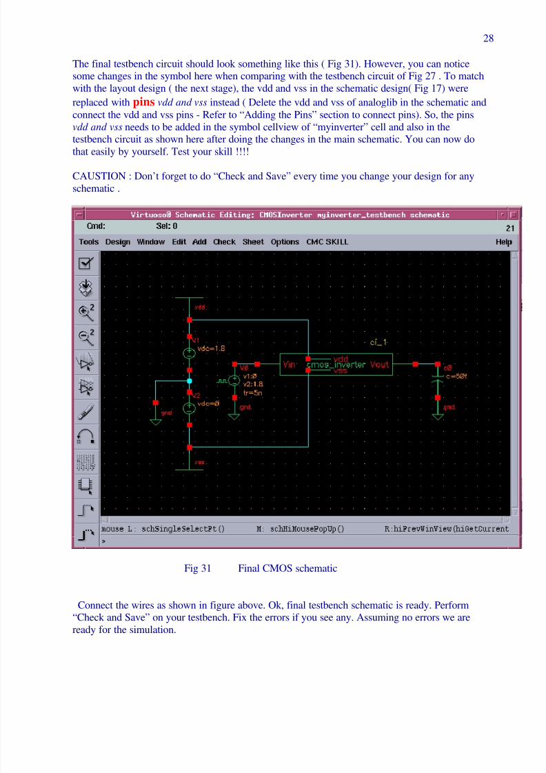
The final testbench circuit should look something like this ( Fig 31). However, you can noticesome changes in the symbol here when comparing with the testbench circuit of Fig 27 . To match
with the layout design ( the next stage), the vdd and vss in the schematic design( Fig 17) were
replaced with pins vdd and vss instead ( Delete the vdd and vss of analoglib in the schematic and
connect the vdd and vss pins - Refer to “Adding the Pins” section to connect pins). So, the pins
vdd and vss needs to be added in the symbol cellview of “myinverter” cell and also in the
testbench circuit as shown here after doing the changes in the main schematic. You can now dothat easily by yourself. Test your skill !!!!
CAUSTION : Don’t forget to do “Check and Save” every time you change your design for any
schematic .
Fig 31 Final CMOS schematic
Connect the wires as shown in figure above. Ok, final testbench schematic is ready. Perform“Check and Save” on your testbench. Fix the errors if you see any. Assuming no errors we are
ready for the simulation.

8/2/2019 Virtuoso Tut 1
http://slidepdf.com/reader/full/virtuoso-tut-1 29/44
29
Let’s now perform the simulation on the testbench circuit to see the final results !!!
SIMULATION
In the Virtuoso Schematic window (the above window one which has symbol cellview“myinverter_symbol”) go to
Tools -> Analog Environment. You will get “Virtuoso Analog Design Environment (1)” (alsoknown as “Virtuoso Analog Artist”) window (Fig 32).
Fig 32 Analog Design Enviornment
First we need to choose the simulator, we will choose Spectre. In the “Virtuoso Analog Design
Environment (1)” window, go to Setup -> Simulator/Directory/Host, and choose Spectre in the
pop-up window( Fig 33), then click OK: (Spectre is similar to spice)

8/2/2019 Virtuoso Tut 1
http://slidepdf.com/reader/full/virtuoso-tut-1 30/44
30
Fig 33 Simulator ( Spectre)
In the Virtuoso Analog Design Environment, go to “Setup -> Model Libraries……… ”.
Enter following path in the box under the “Model Library file”
/home/cadence/kits/cmosp18/models/spectre/icfspectre.init
See Fig 34. Click on “Add” button. Then click OK.
Fig 34 Model Library Setup
Now you need to choose the type of simulation. From “Virtouso Analog Artist”( Fig 32) go toAnalyses -> Choose... ( Fig 35). In this case we will choose a transient analysis. Enter the stop
time for transient analysis. Let’s type 500n for stop time. Click OK.

8/2/2019 Virtuoso Tut 1
http://slidepdf.com/reader/full/virtuoso-tut-1 31/44
31
Fig 35 Choosing Analysis
Now in the “Virtouso Analog Artist” (Fig 32)go to “Outputs -> to be plotted -> select onschematic”. That will bring your testbench cellview window in front. Select node voltages by
clicking on the net. We will click on input and output nets(wires) to select input and output
voltages. The currents can be selected by clicking on the terminals(red squares). If you arepressing right on the pins a circle should appear around each chosen pin. Ok, Look at your
“Analog Artist” window( Fig 36). Did you notice something written under the “Outputs” ? net3
and net6 represents the input and output node voltages respectively.

8/2/2019 Virtuoso Tut 1
http://slidepdf.com/reader/full/virtuoso-tut-1 32/44
32
Fig 36 net 3 and net 6 “Outputs”
Now we can finally simulate! Click on the “Netlist and Run Simulation” button (looks like a green
light) on the right or go to “Simulation -> Netlist and Run”.
It will start simulation. You will need to wait for a while. You should check your “icfb” windowfor messages while it is running the simulation.
In case you have errors you will need to go back and correct them. This can be tricky!
CAUTION Each time you change the schematic you have to do Check and Save!.
You should finally get the desired simulation results, input and output square waves!
( Fig 37).You can zoom in particular portion of your waveforms ( Fig 38) and find out the risetime, fall time, delay of the output waveforms. Remember that we have applied a vpulse source
with particular values of rise time, fall time, delay, period to the CMOS Inverter circuit and wewill get the output with certain rise time, fall time and delay. Later on you can perform
optimizations to your design ( circuit).

8/2/2019 Virtuoso Tut 1
http://slidepdf.com/reader/full/virtuoso-tut-1 33/44
33
Fig 37 Simulation Results
You can zoom in your waveforms. Here is the “zoomed in” waveforms.

8/2/2019 Virtuoso Tut 1
http://slidepdf.com/reader/full/virtuoso-tut-1 34/44
34
Fig 38 Zoomed in Waveforms of Simulation Results
“It's a good idea to save the state of your simulation before you exit the simulation window. You
can do that by going to Session -> Save State (Fig 36). This will be helpful if you want to redo anyof the simulations without having to re-enter everything from scratch. Type state1 as state and
click Ok ( Fig 39).”1
1 Reference A

8/2/2019 Virtuoso Tut 1
http://slidepdf.com/reader/full/virtuoso-tut-1 35/44
35
Fig 39 Saving State
PRINTING AND PLOTTING
“To print the schematic in Virtuoso Schematic from the menu bar along the top, go to Design ->
Plot -> Submit. On this menu there are a lot of options, so you can print a lot of ways. Click onhelp for more details. What I usually do is to write the schematic to a postscript file, then print, in
this way you can have access to the file in the future without having to start Cadence:
1. uncheck Plot With header (if checked)
2. click on plot options - another form pops up
3. check Center Plot
4. click on Fit To Page5. check Send Plot Only to File, enter a file path, e.g., myinverter_schematic.ps OR
myinverter_symbol.ps. This will save the file (.ps file) under the current directory you areworking ( one from where you run your cadence at the consol)
6. uncheck Mail Log To (if checked)
7. click OK on the second window, click OK on the first window”1
Later on you can open your .ps file in the Ghostview program from the directory where it is saved
and you can print it.
If you are working thro’ windows with remote login, you can capture the screen image using“Print Screen” button on the keyboard. You can paste that image in the “Paint” program, modify
the image and then you can save as .bmp and then print it.
You can save the Waveform. To save, on the waveform viewer menu go to File->Save as Image.
Browse the folder where you want to save the image. You have different options to save thewaveform as .bmp or other type of image. Save as whatever option you prefer. Later on you can
open and print the image using appropriate computer program.
1 Reference A

8/2/2019 Virtuoso Tut 1
http://slidepdf.com/reader/full/virtuoso-tut-1 36/44
36
Congratulations, this is the end of Tutorial1.
REFERENCES
Reference A : Cadence Tutorial 1 :
University of Virginia, USA
Reference B : Schematic Entry & Digital Simulation ( Cadence Tutorial) :
Royal Military College of Canada
APPENDIX 1
By: Javid Jaffari ( [email protected])
Parameter Analysis:Suppose that one wants to have the waveforms for various transistor sizing or any other
parameters. One way is to change the corresponding parameter for each simulation, save the
schematic, and run the simulation. However, this is not an appropriate way. Cadence has provideda parameter analysis feature. This feature enables assigning some variables to required parameter.
This enables analysis the effects of sweeping a parameter on the circuit performance.
For example suppose that we want to see the effect of transistor sizing on the propagation delay of
the inverter. To perform this task these steps should be followed:
1- Select the NMOS transistor and push ‘q’ to open its property window.
2- In the Width field enter “Wn” instead of actual value as shown in fig 1, and click OK.
3- Do the same for PMOS transistor; however, to keep the ratio between width of the pmosand nmos constant, you can enter “2*Wn” or “any other number*Wn” in the width field.
4- Save the schematic.5- Open the Analog Design Environment where you use it for running simulations.
6- Do any setting needs to be done same as selecting “tran” type of analysis and simulator
engine “Spectre” and model libraries.
7- Variables Copy from Cellview
8- The list of variables will become visible in the bottom-left side of the window.9- You may here set any desired value to these variables by double clicking on them, and run
simulation. However, to do parameter analysis you don’t need to enter any values here.10- Tools Parametric Analysis…, A new window will be opened.
11- Setup Peak Name For Variable Sweep1…
12- Select “Wn”, OK.13- Fill the “From”, “To”, and “Total Steps” with desired values. Let choose 500n, 2000n, 5,
respectively. As shown in Fig 2.
14- Analysis Start

8/2/2019 Virtuoso Tut 1
http://slidepdf.com/reader/full/virtuoso-tut-1 37/44
37
15- You will find the simulation which running for a range of “Wn” from 500 nm to 2000nmin 5 steps. Results for the output of the inverter are given in Fig.3.
You may do this kind of parameter analysis for any other parameters (e.g. output load capacitance,vdd, …).
Figure 1

8/2/2019 Virtuoso Tut 1
http://slidepdf.com/reader/full/virtuoso-tut-1 38/44
38
Figure 2
Figure 3

8/2/2019 Virtuoso Tut 1
http://slidepdf.com/reader/full/virtuoso-tut-1 39/44
39
Passing Parameters through the HierarchyThis is another feature of Cadence.
When you want to have access to some specific parameters from a symbol abstraction level, youmay use this feature. The feature allows user to pass specific values to each instance’s parameter
of a symbol separately.
For example suppose that you want to have different inverters with different transistor widths, butobviously with the same schematics.
The solution is to write pPar(“Wp”) and pPar(“Wn”) in the field of width of property windows of
PMOS and NMOS devices. Then create a new symbol. This new symbol has the ability to get twovalues for Wp and Wn and assign to the width of the transistors.
_______________________________________________________________________________
APPENDIX 2
Using Calculator and Expressions for Parameter Analysis and Optimization
Cadence provides some useful features to do optimization and parametric analysis on circuits.Following, we solve a problem by using calculator and defining expressions.
Problem: Find the (W P / W N ) ratio of a CMOS inverter which minimizes the propagation delay of
the gate.
Discussion: It is known that the minimum delay CMOS does not necessarily correspond to
symmetric or equal t pHL, t pLH design. Therefore, the objective will be minimizing the (t pHL, t pLH )/2directly.
Assumptions: Output capacitive load = 10 fF V DD=1.8v W N =600 nm t r =t f =20 pS.
Methodologies:
Approach 1) Parametric Analysis:
1. Create a CMOS Inverter.
2. Assign “ratiox600 nm” to the PMOS width. (Note that here “ratio will be the variable whichwe want to find in order to make delay minimum”)
3. Create a chain shape test circuit schematic for the inverter corresponding to the given
assumptions as shown below: (Assign names to the input and output wires to make them easilytraceable)

8/2/2019 Virtuoso Tut 1
http://slidepdf.com/reader/full/virtuoso-tut-1 40/44
40
4. In the “Analog Design Environment” perform “model library” and “choose analyses” setting
(transient).
5. In the “Analog Design Environment”, Outputs->Setup…6. In the “Setting Outputs”, Name (opt.)=tpHL. Below picture:
7. Click Calculator “Open”. The Calculator window will be opened.
8. In “Calculator” window, Options->Set PRN, to remove the tick.
9. In “Calculator” window, Tools->Browser, The result browser will be opened. (Note that you
had to ran the simulation one time before to see the signals in the browser)10. In “Calculator” window, there is a list of functions click “delay”.
11. In “Result Browser” window, open “tran-tran”. The two windows will be like below:
12.
Place the cursor in the Signal 1 textbox.13. Click “InSig” from “Results Browser”.
14. Place the cursor in the Signal 2 textbox.15. Click “OutSig” from “Results Browser”.
16. Change the Thershold Value 1 to 0.9 which is (V DD /2).
17. Change the Edge Type 1 to “rising”
18. Click >>>19. Change the Thershold Value 2 to 0.9 which is (V DD /2).
20. Change the Edge Type 2 to “falling”
21. Click >>>

8/2/2019 Virtuoso Tut 1
http://slidepdf.com/reader/full/virtuoso-tut-1 41/44
41
22. Click Apply23. In the “Setting Outputs” window, Click “Get Expression”, then “Add”. An expression for t pHL
has been added.
24. Repeat previous steps this time for tpLH, but assign “falling” to Edge Type 1 and “rising” toEdge Type 2.
25. Now you have two expressions in the “Setting Outputs” window. Like below:
26. Now create an expression namely, “Delay” which is equal to ( t pLH +t pHL)/2. To do this, we mustfollow the same way we did for tpHL and tpLH and use “(”, “)”, “+”, and “/” buttons when are
needed. (You need to redo steps to define delays from 12 to 22). Following is the picture of the
“Setting Outputs” window after adding three expressions.
27. Go back to “Analog design Environment” window. You will see that the three expressions are
listed.
28. Tools -> Parametric Analysis…, A new window will be opened.
29. In the “Parametric Analysis”, Setup->Peak Name For Variable->Sweep1…30. Select “ratio”, OK.
31. Fill the “From”, “To”, and “Total Steps” with desired values. Let choose 0.5, 4, 10,
respectively. As shown in below. Change Step Control to Logarithmic.
32. Analysis -> Star
33. The output will be the plot of three parameters for different PMOS/NMOS width ratios.This is the output plot. It can be seen that the minimum delay ratio does not necessarily
correspond to the symmetrical point.

8/2/2019 Virtuoso Tut 1
http://slidepdf.com/reader/full/virtuoso-tut-1 42/44
42
The ratio which gives the minimum delay is 1.765. And the corresponding delay will be 23.74
pSec. However the ratio which t pLH =t pHL is 2.638 for this case.
Approach 2) Optimization:
Follow steps (1)-(27) of the first approach.
28. Tools -> Optimization…, A new window will be opened.29. In the “Analog Circuit Optimizer” window, Goals->Retrieve Outputs…, Then the three
defined expression will be listed.
30. Delete “tpHL” and “tpLH” and just keep “Delay”31. Double click on “Delay”
32. Choose direction as minimize.
33. Set a target for delay. Let say 20p.
34. Set the acceptable to 23p.35. Hit OK.
36. In the “Analog Circuit Optimizer” window, Variables->Add/Edit…, Select “ratio”. Assign
initial value 0.5, minimum 0.5, and maximum 5. The window should become same as below:

8/2/2019 Virtuoso Tut 1
http://slidepdf.com/reader/full/virtuoso-tut-1 43/44
43
37. Optimizer->Run
The output will be a graph of ratio and delay for every iteration. You may stop the optimizer when
it doesn’t give better result. (You should be aware that due to very nonlinear nature of thesimulations, the optimization may converge to some local minima, therefore you may need to
change the initial value of skip such local optimums).Here is the sample output graph for our problem.
Go Back
-Appendix 1 & 2 by - Mr. Javid Jaffari

8/2/2019 Virtuoso Tut 1
http://slidepdf.com/reader/full/virtuoso-tut-1 44/44
44