visual system simulator - awrcorp.com€™s visual system simulator co ... the resulting spectrum...
TRANSCRIPT
Advancing the Wireless Revolution with AWR and NI Software
AWR’S VISUAL SYSTEM SIMULATOR CO-SIMULATES WITH NI’S LABVIEW FOR ENHANCED SIGNAL PROCESSING CAPABILITIES
Achieving the highest possible performance from circuits used in third-and
fourth-generation wireless systems is driving a tighter integration of previously
disparate tools. Certainly, a level of software synergy is essential when
designing circuits for use in today’s wireless systems that employ higher-order
modulation techniques together with advanced technologies, such as Orthogonal
Frequency Division Multiplexing (OFDM), multiple-input multiple-output (MIMO)
and digital predistortion (DPD) circuits, to name a few. As this white paper
illustrates, AWR’s Visual System Simulator (VSS) and National Instruments’
LabVieW graphical programming environment are now co-simulating so as to
better enable designers to analyze, optimize, and verify complex RF circuits,
subsystems and digital signal processing within a unifi ed framework.
Before looking more closely into specifi c design scenarios, it is important
to understand how this new and cohesive VSS/LabVIEW co-simulation
environment works.
HOW IT WORKS
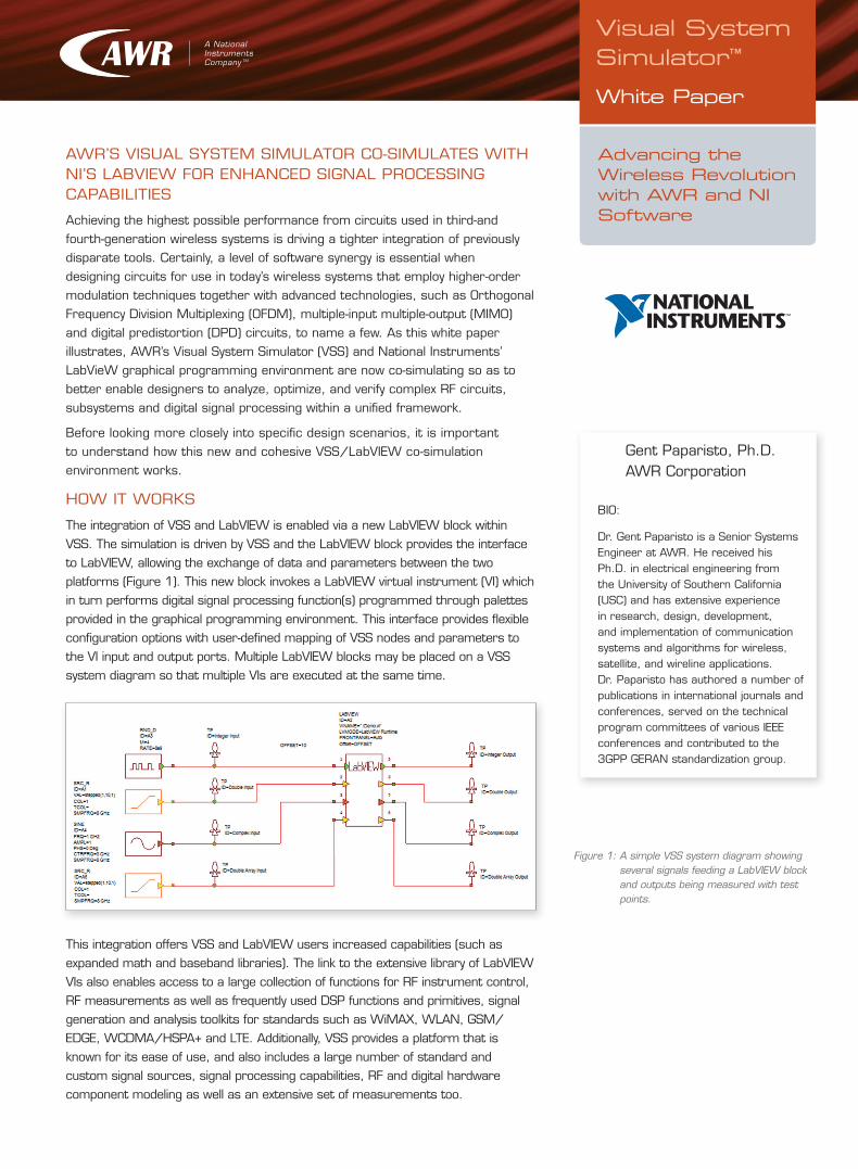
The integration of VSS and LabVIEW is enabled via a new LabVIEW block within
VSS. The simulation is driven by VSS and the LabVIEW block provides the interface
to LabVIEW, allowing the exchange of data and parameters between the two
platforms (Figure 1). This new block invokes a LabVIEW virtual instrument (VI) which
in turn performs digital signal processing function(s) programmed through palettes
provided in the graphical programming environment. This interface provides fl exible
confi guration options with user-defi ned mapping of VSS nodes and parameters to
the VI input and output ports. Multiple LabVIEW blocks may be placed on a VSS
system diagram so that multiple VIs are executed at the same time.
This integration offers VSS and LabVIEW users increased capabilities (such as
expanded math and baseband libraries). The link to the extensive library of LabVIEW
VIs also enables access to a large collection of functions for RF instrument control,
RF measurements as well as frequently used DSP functions and primitives, signal
generation and analysis toolkits for standards such as WiMAX, WLAN, GSM/
EDGE, WCDMA/HSPA+ and LTE. Additionally, VSS provides a platform that is
known for its ease of use, and also includes a large number of standard and
custom signal sources, signal processing capabilities, RF and digital hardware
component modeling as well as an extensive set of measurements too.
Visual SystemSimulator™
White Paper
Gent Paparisto, Ph.D.AWR Corporation
BIO:
Dr. Gent Paparisto is a Senior Systems Engineer at AWR. He received his Ph.D. in electrical engineering from the University of Southern California (USC) and has extensive experience in research, design, development, and implementation of communication systems and algorithms for wireless, satellite, and wireline applications. Dr. Paparisto has authored a number of publications in international journals and conferences, served on the technical program committees of various IEEE conferences and contributed to the 3GPP GERAN standardization group.
Figure 1: A simple VSS system diagram showing several signals feeding a LabVIEW block and outputs being measured with test points.

There are two options for interfacing with LabVIEW in VSS.
1. Use the LabVIEW Run-Time Engine for executing a VI -- provides
for fast simulation times but disables the creation, modifi cation or
debugging of VIs.
2. Connect to the LabVIEW Development System -- provides full fl exibility for
creation, modifi cation and debugging of VIs as necessary.
This interface further allows for the use of LabVIEW add-ons and
toolkits, which provide standard signal sources and measurements,
signal processing, analysis and connectivity, integration with
development hardware, and many other capabilities. Taking a
closer look as to how designers may utilize this new co-simulation
environment, the following scenarios are presented.
SCENARIO 1: SIGNAL PROCESSING BLOCKS
VSS can generate signals required for the design and simulation of
modern communication systems. Real, complex, and digital signal
sources can be combined to provide real-world emulation of signals for a
wide range of applications. Figure 2 shows a VSS system diagram with
several of these signals feeding a LabVIEW block (red circle in Figure 2)
and outputs being measured with test points (blue box inset into Figure 2).
The LabVIEW block ties directly to a VI in LabVIEW. The link between VSS
and LabVIEW is managed exclusively by this block. During VSS simulation,
the time-domain data is fed into the LabVIEW data fl ow and the resulting
VI ouput is resynchronized in time with the VSS simulation. Referring to
Figure 2, the integer data in VSS goes to LabVIEW and its amplitude is
calculated with a summing function and returned to VSS. The resulting
output (Figure 3) - relative to the input - is scaled in amplitude according
to the LabVIEW processing block. The real and complex signals have a
similar operation.
Additionally, LabVIEW VIs can also be used from within the VSS
environment. Consider a simple VI that takes two input signals, adds
them together, and scales the result by a variable gain that is set by a
user-controlled slider (Figure 4). Here, this VI is converted to a “subVI”
by assigning Input 1 and Input 2 numeric controls as input terminals and
Output as an output terminal in the connector pane. This VI can then be
used in a VSS system diagram with a LabVIEW block confi gured to the
desired VI, and the input and output nodes that will interface with the VI
are added. In essence, the controls and indicators in LabVIEW become
inputs and outputs, respectively, in VSS. This is accomplished by clicking
“Add” under the Input Ports section, selecting the nodes from available
input ports defi ned in the VI, and if desired defi ning a name for each port.
The output port is also added and the property propagation is defi ned.
This simulation also uses the LabVIEW Run-Time Engine and shows
the VI front panel. The input to the VI consists of two tones: 1 and
1.1 GHz. The results are displayed on a graph in the LabVIEW
front panel window, as defi ned in the VI (Figure 5). This window is
automatically opened during the simulation. The results will display
immediately on a VSS graph as well.
(additional positioning line here ???)AXIEMVisual SystemSimulator
White Paper
Figure 2: The view shows how the LabVIEW block ties directly to a VI in LabVIEW.
Figure 3: The resulting output relative to the input is scaled in amplitude according to the LabVIEW processing block.
Figure 5: LabVIEW front panel window displayed within VSS.
Figure 4: User-controlled slider within LabVIEW VI.

SCENARIO 2: A DIGITAL PREDISTORTION (DPD) EXAMPLE
Digital predistortion techniques, employed to overcome the nonlinear
operation of base station amplifi ers, have become a mandatory
component to support today’s wider bandwidth signals, high power
effi ciency and output linearity requirements. VSS provides an
environment for generating input signals, modeling the circuit-level
amplifi er, as well as performing the required measurements. It also
offers the ability to design a DPD proof-of-concept and then convert it
from fl oating-point to a realistic fi xed-point implementation. LabVIEW
includes many of these signal processing capabilities as well but
also offers the option of implementing the resulting design in an
FPGA. In this way, users are greatly aided by the joint VSS/LabVIEW
environment in that it allows for faster design thru to prototype and
test of fi nal DPD implementations.
In this scenario, the predistortion circuit uses digitally-controlled
attenuators and phase shifters and its implementation is moved very
early in the design process to LabVIEW given the new VSS/LabVIEW
unifi ed framework. Based on a circuit-level amplifi er, a VI is created
that takes a sample of the signal passing through the amplifi er and
creates a predistorted signal. This signal is passed back to VSS where
it enters the amplifi er so the resulting signal is more linear. This
process benefi ts designers in that it provides a seamless methodology
that allows for successively adding more complexity to the circuit while
concurrently evaluating its performance.
Figure 6 shows a 1900 MHz power amplifi er from AWR’s library.
The AM/AM and AM/PM curves are shown in Figure 7 along with
the resulting spectrum with QPSK modulation at a power level with
notable distortion (visible as spectral regrowth “side lobes”) simulated
in VSS as a reference. There are two foundational aspects of digital
predistortion that need to be addressed for the technique to work.
A sample of the amplifi er’s input-output characteristics must be available
in order to determine what must be corrected. This can be done by
periodically running the digital predistortion circuit in a calibration mode
to characterize the amplifi er, or by sampling the amplifi er’s output and
building a characterization table dynamically over time.
In this case, the discussion concerns an early stage of the design
process when only the amplifi er is being simulated. A copy of the
amplifi er can be used to create the characterization dynamically
before the signal reaches the actual amplifi er simulation. This is
shown in Figure 8, which is a VSS system diagram in which a copy of
the 1900 MHz amplifi er (element S1, circled in Figure 8) is placed
early in the signal path where the signal is predistorted.
The second issue that must be addressed is the amount of correction
required to predistort the signal. While this can be achieved
algorithmically by understanding the AM/AM and AM/PM behavior,
it is being done manually within the VI to illustrate the functionality.
(additional positioning line here ???)AXIEMVisual SystemSimulator
White Paper
Figure 6: Circuit-level schematic of the1900 MHz power amplifi er.
Figure 7: AM/AM and AM/PM curves from the amplifi er along with the resulting spectrum with QPSK modulation at a nominal power level simulated in VSS as a reference.
Figure 8: A VSS system diagram of the 1900 MHz amplifi er when placed early in the signal path where the signal is predistorted.

Here, LabVIEW’s benefi ts become clear as the design fl ow moves
toward actual hardware, as the VI can be made more realistic by
adding corrective algorithms and extending this VI to measure the
attenuators, phase shifters, and other components that would
otherwise only be modeled in the VSS system diagram.
One of the benefi ts of the synergy between VSS and LabVIEW is
in the ability of VSS to capture the simulated 1900 MHz amplifi er
and LabVIEW to capture the actual attenuators and phase shifters.
The user can determine when and how to switch from manual to
algorithmic behavior given the challenges and progress of the design
fl ow. The LabVIEW VI is added to the VSS system diagram to create
the predistorted signal (Figure 9). The VSS input signal is transferred
through the LabVIEW block to the VI and separated into phase and
magnitude. These signals are then used early in the development of
the predistortion circuit to drive a look-up table or simple continuous
algorithm corresponding to the phase and magnitude of the output
signal. Operating on the complex signal (as phase and magnitude)
allows direct implementation of the phase shifter and attenuator. As
the digital phase shifter and attenuator are digitally controlled, the
look-up table can be implemented in an FPGA for easy recalibration
or updating as determined by system performance.
First-pass predistorter results are shown in Figure 10. The blue
trace shows the signal as it would appear without predistortion,
while the red trace shows an early manual correction using the
LabVIEW VI to alter the phase and magnitude as a predistortion
function. The improvement is seen in the spectral mask, where
regrowth is reduced by about 25 dB. As the amplifi er is driven
harder, the performance should be even more pronounced thereby
maintaining the linearity of the amplifi er at higher power levels.
SUMMARY
Achieving the highest possible performance from circuits used
in third-and fourth-generation wireless systems requires the
seamless integration of simulation and measurement at every
stage of the design process. Designers who deviate from this are
at risk as the further in the design process that serious design
issues are discovered, the more time (and money) it will take to
remedy them. AWR’s VSS software and National Instruments’
LabVIEW signifi cantly reduce the possibility that the latter scenario
will occur, as the circuit and its components are passed back
and forth seamlessly between the two tools. The result is better
performance, shorter design time, and a minimum of frustration.
(additional positioning line here ???)AXIEMVisual SystemSimulator
White Paper
Figure 9: A LabVIEW VI added to the VSS system diagram to create the predistorted signal.
AWR, 1960 East Grand Avenue, Suite 430, El Segundo, CA 90245, USATel: +1 (310) 726-3000 Fax: +1 (310) 726-3005 www.awrcorp.com
Copyright © 2012 AWR Corp. All rights reserved. AWR is a National Instruments Company. AWR, and the AWR logo are registered trademarks and Visual System Simulator is a trademark of AWR Corporation. All others are trademarks of their respective holders. WP-VSS-NI-2012.5.31
Figure 10: First-pass predistorter results. The blue trace shows the signal as it would appear without predistortion, while the red trace shows an early manual correction using the LabVIEW VI to alter the phase and magnitude as a predistortion function. The improvement is seen in the spectral mask, where regrowth is reduced by about 25 dB.
View the AWRVSS/LabVIEW Integration video on AWR.TV.