volume 1 part 1: graphics core -...
TRANSCRIPT

Doc Ref #: IHD_OS_V1Pt1_3_10
Intel® OpenSource HD Graphics PRM Volume 1 Part 1: Graphics Core
For the all new 2010 Intel Core Processor Family Programmer’s Reference Manual (PRM)
March 2010 Revision 1.0

2 Doc Ref #: IHD_OS_V1Pt1_3_10
Creative Commons License
You are free:
to Share — to copy, distribute, display, and perform the work
Under the following conditions:
Attribution. You must attribute the work in the manner specified by the author or licensor (but not in any
way that suggests that they endorse you or your use of the work).
No Derivative Works. You may not alter, transform, or build upon this work.
INFORMATION IN THIS DOCUMENT IS PROVIDED IN CONNECTION WITH INTEL® PRODUCTS. NO LICENSE, EXPRESS OR IMPLIED, BY ESTOPPEL OR OTHERWISE, TO ANY INTELLECTUAL PROPERTY RIGHTS IS GRANTED BY THIS DOCUMENT. EXCEPT AS PROVIDED IN INTEL’S TERMS AND CONDITIONS OF SALE FOR SUCH PRODUCTS, INTEL ASSUMES NO LIABILITY WHATSOEVER, AND INTEL DISCLAIMS ANY EXPRESS OR IMPLIED WARRANTY, RELATING TO SALE AND/OR USE OF INTEL PRODUCTS INCLUDING LIABILITY OR WARRANTIES RELATING TO FITNESS FOR A PARTICULAR PURPOSE, MERCHANTABILITY, OR INFRINGEMENT OF ANY PATENT, COPYRIGHT OR OTHER INTELLECTUAL PROPERTY RIGHT. Intel products are not intended for use in medical, life saving, or life sustaining applications. Intel may make changes to specifications and product descriptions at any time, without notice. Designers must not rely on the absence or characteristics of any features or instructions marked "reserved" or "undefined." Intel reserves these for future definition and shall have no responsibility whatsoever for conflicts or incompatibilities arising from future changes to them. The Sandy Bridge chipset family, Havendale/Auburndale chipset family, Intel® 965 Express Chipset Family, Intel® G35 Express Chipset, and Intel® 965GMx Chipset Mobile Family Graphics Controller may contain design defects or errors known as errata which may cause the product to deviate from published specifications. Current characterized errata are available on request. Contact your local Intel sales office or your distributor to obtain the latest specifications and before placing your product order. I2C is a two-wire communications bus/protocol developed by Philips. SMBus is a subset of the I2C bus/protocol and was developed by Intel. Implementations of the I2C bus/protocol may require licenses from various entities, including Philips Electronics N.V. and North American Philips Corporation. Intel and the Intel are trademarks of Intel Corporation in the U.S. and other countries. *Other names and brands may be claimed as the property of others. Copyright © 2010, Intel Corporation. All rights reserved.

Doc Ref #: IHD_OS_V1Pt1_3_10 3
Revision History Document Number Revision Number Description Revision Date
IHD_OS_V1Pt1_3_10 1..0 First Release. March 2010
§§

4 Doc Ref #: IHD_OS_V1Pt1_3_10
Contents 1. Introduction ............................................................................................................................................7
1.1 Reserved Bits and Software Compatibility ...........................................................................................9 1.2 Terminology..........................................................................................................................................9
2. Graphics Device Overview..................................................................................................................18 2.1 Graphics Memory Controller Hub (GMCH) ........................................................................................18 2.2 Graphics Processing Unit (GPU)........................................................................................................19
3. Graphics Processing Engine (GPE)...................................................................................................21 3.1 Introduction .........................................................................................................................................21 3.2 Overview.............................................................................................................................................21
3.2.1 Block Diagram ..............................................................................................................................22 3.2.2 Command Stream (CS) Unit.........................................................................................................23 3.2.3 3D Pipeline ...................................................................................................................................23 3.2.4 Media Pipeline ..............................................................................................................................24 3.2.5 GENX Subsystem.........................................................................................................................24 3.2.6 GPE Function IDs .........................................................................................................................24
3.3 Pipeline Selection ...............................................................................................................................25 3.4 URB Allocation....................................................................................................................................26
3.4.1 URB_FENCE ................................................................................................................................26 3.5 Constant URB Entries (CURBEs).......................................................................................................32
3.5.1 Overview.......................................................................................................................................32 3.5.2 Multiple CURBE Allocation ...........................................................................................................32 3.5.3 CS_URB_STATE..........................................................................................................................33 3.5.4 CONSTANT_BUFFER..................................................................................................................34 3.5.5 MEMORY_OBJECT_CONTROL_STATE....................................................................................36
3.6 Memory Access Indirection ................................................................................................................37 3.6.1 STATE_BASE_ADDRESS ...........................................................................................................40
3.7 State Invalidation ([DevCTG+]) ..........................................................................................................47 3.7.1 STATE_POINTER_INVALIDATE ([DevCTG+]) ...........................................................................47
3.8 Instruction and State Prefetch ............................................................................................................49 3.8.1 STATE_PREFETCH.....................................................................................................................49
3.9 System Thread Configuration.............................................................................................................51 3.9.1 STATE_SIP ..................................................................................................................................51
3.10 Command Ordering Rules ................................................................................................................52 3.10.1 PIPELINE_SELECT....................................................................................................................52 3.10.2 PIPE_CONTROL........................................................................................................................52 3.10.3 URB-Related State-Setting Commands .....................................................................................53 3.10.4 Common Pipeline State-Setting Commands..............................................................................53 3.10.5 3D Pipeline-Specific State-Setting Commands ..........................................................................54 3.10.6 Media Pipeline-Specific State-Setting Commands.....................................................................54 3.10.7 URB_FENCE (URB Fencing & Entry Allocation)........................................................................55 3.10.8 CONSTANT_BUFFER (CURBE Load) ......................................................................................56 3.10.9 3DPRIMITIVE .............................................................................................................................56 3.10.10 MEDIA_OBJECT ......................................................................................................................56
3.11 Video Command Streamer (VCS).....................................................................................................56 4. Graphics Command Formats .............................................................................................................58
4.1 Command Formats.............................................................................................................................58 4.1.1 Memory Interface Commands ......................................................................................................59 4.1.2 2D Commands..............................................................................................................................59

Doc Ref #: IHD_OS_V1Pt1_3_10 5
4.1.3 3D/Media Commands...................................................................................................................59 4.1.4 Video Codec Commands..............................................................................................................59 4.1.5 Command Header ........................................................................................................................60
4.2 Command Map ...................................................................................................................................61 4.2.1 Memory Interface Command Map ................................................................................................61 4.2.2 2D Command Map........................................................................................................................63 4.2.3 3D/Media Command Map.............................................................................................................64 4.2.4 Video Codec Command Map .......................................................................................................67
5. Register Address Maps.......................................................................................................................69 5.1 Graphics Register Address Map.........................................................................................................69
5.1.1 Memory and I/O Space Registers ................................................................................................69 5.1.2 PCI Configuration Space ..............................................................................................................71 5.1.3 Graphics Register Memory Address Map.....................................................................................71
5.2 VGA and Extended VGA Register Map..............................................................................................71 5.2.1 VGA and Extended VGA I/O and Memory Register Map.............................................................71
5.3 Indirect VGA and Extended VGA Register Indices ............................................................................73 6. Memory Data Formats .........................................................................................................................76
6.1 Memory Object Overview ...................................................................................................................76 6.1.1 Memory Object Types...................................................................................................................76
6.2 Channel Formats ................................................................................................................................77 6.2.1 Unsigned Normalized (UNORM) ..................................................................................................77 6.2.2 Gamma Conversion (SRGB) ........................................................................................................77 6.2.3 Signed Normalized (SNORM) ......................................................................................................78 6.2.4 Unsigned Integer (UINT/USCALED) ............................................................................................78 6.2.5 Signed Integer (SINT/SSCALED).................................................................................................78 6.2.6 Floating Point (FLOAT).................................................................................................................78
6.3 Non-Video Surface Formats ...............................................................................................................81 6.3.1 Surface Format Naming................................................................................................................82 6.3.2 Intensity Formats ..........................................................................................................................82 6.3.3 Luminance Formats ......................................................................................................................82 6.3.4 R1_UNORM (same as R1_UINT) and MONO8 ...........................................................................82 6.3.5 Palette Formats ............................................................................................................................83
6.4 Compressed Surface Formats............................................................................................................86 6.4.1 FXT Texture Formats....................................................................................................................86 6.4.2 BC4............................................................................................................................................ 100 6.4.3 BC5............................................................................................................................................ 102
6.5 Video Pixel/Texel Formats............................................................................................................... 103 6.5.1 Packed Memory Organization ................................................................................................... 103 6.5.2 Planar Memory Organization..................................................................................................... 104
6.6 Surface Memory Organizations ....................................................................................................... 106 6.7 Graphics Translation Tables............................................................................................................ 107 6.8 Hardware Status Page .................................................................................................................... 107 6.9 Instruction Ring Buffers ................................................................................................................... 107 6.10 Instruction Batch Buffers................................................................................................................ 107 6.11 Display, Overlay, Cursor Surfaces................................................................................................. 108 6.12 2D Render Surfaces ...................................................................................................................... 108 6.13 2D Monochrome Source ................................................................................................................ 108 6.14 2D Color Pattern ............................................................................................................................ 108 6.15 3D Color Buffer (Destination) Surfaces ......................................................................................... 109 6.16 3D Depth Buffer Surfaces .............................................................................................................. 109 6.17 3D Separate Stencil Buffer Surfaces [ILK+] .................................................................................. 109 6.18 Surface Layout ............................................................................................................................... 110
6.18.1 Buffers...................................................................................................................................... 110

6 Doc Ref #: IHD_OS_V1Pt1_3_10
6.18.2 1D Surfaces ............................................................................................................................. 111 6.18.3 2D Surfaces ............................................................................................................................. 111 6.18.4 Cube Surfaces ......................................................................................................................... 116 6.18.5 3D Surfaces ............................................................................................................................. 118
6.19 Surface Padding Requirements..................................................................................................... 119 6.19.1 Sampling Engine Surfaces ...................................................................................................... 119 6.19.2 Render Target and Media Surfaces ........................................................................................ 120

Doc Ref #: IHD_OS_V1Pt1_3_10 7
1. Introduction The Intel® HD Graphics Open Source (PRM) describes the architectural behavior and programming environment of the Havendale/Auburndale chipset family. The Graphics Controller (GC) contains an extensive set of registers and instructions for configuration, 2D, 3D, and Video systems. The PRM describes the register, instruction, and memory interfaces and the device behaviors as controlled and observed through those interfaces. The PRM also describes the registers and instructions and provides detailed bit/field descriptions.
The Programmer’s Reference Manual is organized into four volumes:
PRM, Volume 1: Graphics Core Volume 1, Part 1, 2, 3, 4 and 5 covers the overall Graphics Processing Unit (GPU), without much detail on 3D, Media, or the core subsystem. Topics include the command streamer, context switching, and memory access (including tiling). The Memory Data Formats can also be found in this volume. The volume also contains a chapter on the Graphics Processing Engine (GPE). The GPE is a collective term for 3D, Media, the subsystem, and the parts of the memory interface that are used by these units. Display, blitter and their memory interfaces are not included in the GPE.
PRM, Volume 2: 3D/Media Volume 2, Part 1, 2 covers the 3D and Media pipelines in detail. This volume is where details for all of the “fixed functions” are covered, including commands processed by the pipelines, fixed-function state structures, and a definition of the inputs (payloads) and outputs of the threads spawned by these units. This volume also covers the single Media Fixed Function, VLD. It describes how to initiate generic threads using the thread spawner (TS). It is generic threads which will be used for doing the majority of media functions. Programmable kernels will handle the algorithms for media functions such IDCT, Motion Compensation, and even Motion Estimation (used for encoding MPEG streams).
PRM, Volume 3: Display Registers Volume 3, Part 1, 2, 3 describes the control registers for the display. The overlay registers and VGA registers are also cover in this volume.
PRM, Volume 4: Subsystem and Cores/Shared Functions Volume 4, Part 1 and 2 describes the GMCH programmable cores, or EUs, and the “shared functions”, which are shared by more than one EU and perform functions such as I/O and complex math functions. The shared functions consist of the sampler: extended math unit, data port (the interface to memory for 3D and media), Unified Return Buffer (URB), and the Message Gateway which is used by EU threads to signal each other. The EUs use messages to send data to and receive data from the subsystem; the messages are described along with the shared functions although the generic message send EU instruction is described with the rest of the instructions in the Instruction Set Architecture (ISA) chapters.

8 Doc Ref #: IHD_OS_V1Pt1_3_10
This latter part of this volume describes the GMCH core, or EU, and the associated instructions that are used to program it. The instruction descriptions make up what is referred to as an Instruction Set Architecture, or ISA. The ISA describes all of the instructions that the GMCH core can execute, along with the registers that are used to store local data.
Device Tags and Chipsets
Device “Tags” are used in various parts of this document as aliases for the device names/steppings, as listed in the following table. Note that stepping info is sometimes appended to the device tag, e.g., [DevBW-C]. Information without any device tagging is applicable to all devices/steppings.
Table 1-1. Supported Chipsets
Chipset Family Name Device Name
Device Tag
Intel® Q965 Chipset Intel® Q963 Chipset Intel® G965 Chipset
82Q965 GMCH 82Q963 GMCH 82G965 GMCH
[DevBW]
Intel® G35 Chipset 82G35 GMCH
[DevBW-E]
Mobile Intel® GME965 Express Chipset Mobile Intel® GM965 Express Chipset Mobile Intel® PM965 Express Chipset Mobile Intel® GL960 Express Chipset
GM965 GMCH GME965 GMCH
[DevCL]
Mobile Intel® GL40/GM45/GS40/GS45 Express Chipset
GL40 GM45 GS40 GS45
[DevCTG], [DevCTG-A] [DevCTG-B]
Intel® G41 Express Chipset Intel® G43 Express Chipset Intel® G45 Express Chipset Intel® Q43 Express Chipset Intel® Q45 Express Chipset
G41 G43 G45 Q43 Q45
[DevEL]
Intel® HD Graphics For the all new 2010 Intel Core™ Processor Family
Intel® Core™ i3 processor, Intel® Core™ i5 processor
[DevHVN/ABD] [DevILK] [DevIL]
NOTES: 1. Unless otherwise specified, the information in this document applies to all of the devices mentioned in Table 1-1. For
Information that does not apply to all devices, the Device Tag is used. 2. Throughout the PRM, references to “All” in a project field refters to all devices in
Table 1-1. 3. Throughout the PRM, references to [DevBW] apply to both [DevBW] and [DevBW-E]. [DevBW-E] is referenced
specifically for information that is [DevBW-E] only. 4. Stepping info is sometimes appended to the device tag (e.g., [DevBW-C]). Information without any device tagging is
applicable to all devices/steppings. 5. A shorthand is used to identify all devices/steppings prior to the device/stepping that the item pertains. Notations and
Conventions.

Doc Ref #: IHD_OS_V1Pt1_3_10 9
1.1 Reserved Bits and Software Compatibility In many register, instruction and memory layout descriptions, certain bits are marked as “Reserved”. When bits are marked as reserved, it is essential for compatibility with future devices that software treat these bits as having a future, though unknown, effect. The behavior of reserved bits should be regarded as not only undefined, but unpredictable. Software should follow these guidelines in dealing with reserved bits: Do not depend on the states of any reserved bits when testing values of registers that contain such bits. Mask out the reserved bits before testing. Do not depend on the states of any reserved bits when storing to instruction or to a register. When loading a register or formatting an instruction, always load the reserved bits with the values indicated in the documentation, if any, or reload them with the values previously read from the register.
1.2 Terminology
Term Abbr. Definition
3D Pipeline -- One of the two pipelines supported in the GPE. The 3D pipeline is a set of fixed-function units arranged in a pipelined fashion, which process 3D-related commands by spawning EU threads. Typically this processing includes rendering primitives. See 3D Pipeline.
Adjacency -- One can consider a single line object as existing in a strip of connected lines. The neighboring line objects are called “adjacent objects”, with the non-shared endpoints called the “adjacent vertices.” The same concept can be applied to a single triangle object, considering it as existing in a mesh of connected triangles. Each triangle shares edges with three other adjacent triangles, each defined by an non-shared adjacent vertex. Knowledge of these adjacent objects/vertices is required by some object processing algorithms (e.g., silhouette edge detection). See 3D Pipeline.
Application IP AIP Application Instruction Pointer. This is part of the control registers for exception handling for a thread. Upon an exception, hardware moves the current IP into this register and then jumps to SIP.
Architectural Register File
ARF A collection of architecturally visible registers for a thread such as address registers, accumulator, flags, notification registers, IP, null, etc. ARF should not be mistaken as just the address registers.
Array of Cores -- Refers to a group of Genx EUs, which are physically organized in two or more rows. The fact that the EUs are arranged in an array is (to a great extent) transparent to CPU software or EU kernels.
Binding Table -- Memory-resident list of pointers to surface state blocks (also in memory).
Binding Table Pointer BTP Pointer to a binding table, specified as an offset from the Surface State Base Address register.
Bypass Mode -- Mode where a given fixed function unit is disabled and forwards data down the pipeline unchanged. Not supported by all FF units.
Byte B A numerical data type of 8 bits, B represents a signed byte integer.
CBOX CBOX Cache Box (Ring stop at LLC).

10 Doc Ref #: IHD_OS_V1Pt1_3_10
Term Abbr. Definition
Child Thread A branch-node or a leaf-node thread that is created by another thread. It is a kind of thread associated with the media fixed function pipeline. A child thread is originated from a thread (the parent) executing on an EU and forwarded to the Thread Dispatcher by the TS unit. A child thread may or may not have child threads depending on whether it is a branch-node or a leaf-node thread. All pre-allocated resources such as URB and scratch memory for a child thread are managed by its parent thread.
Clip Space -- A 4-dimensional coordinate system within which a clipping frustum is defined. Object positions are projected from Clip Space to NDC space via “perspecitive divide” by the W coordinate, and then viewport mapped into Screen Space
Clipper -- 3D fixed function unit that removes invisible portions of the drawing sequence by discarding (culling) primitives or by “replacing” primitives with one or more primitives that replicate only the visible portion of the original primitive.
Color Calculator CC Part of the Data Port shared function, the color calculator performs fixed-function pixel operations (e.g., blending) prior to writing a result pixel into the render cache.
Command -- Directive fetched from a ring buffer in memory by the Command Streamer and routed down a pipeline. Should not be confused with instructions which are fetched by the instruction cache subsystem and executed on an EU.
Command Streamer CS or CSI Functional unit of the Graphics Processing Engine that fetches commands, parses them and routes them to the appropriate pipeline.
Constant URB Entry CURBE A UE that contains “constant” data for use by various stages of the pipeline.
Control Register CR The read-write registers are used for thread mode control and exception handling for a thread.
Data Port DP Shared function unit that performs a majority of the memory access types on behalf of Gen4 programs. The Data Port contains the render cache and the constant cache and performs all memory accesses requested by Gen4 programs except those performed by the Sampler. See DataPort.
Degenerate Object -- Object that is invisible due to coincident vertices or because does not intersect any sample points (usually due to being tiny or a very thin sliver).
Destination -- Describes an output or write operand.
Destination Size The number of data elements in the destination of a Genx SIMD instruction.
Destination Width The size of each of (possibly) many elements of the destination of a GenxxSIMD instruction.
Double Quad word (DQword)
DQ A fundamental data type, DQ represents 16 bytes.
Double word (DWord) D or DW A fundamental data type, D or DW represents 4 bytes.
Drawing Rectangle -- A screen-space rectangle within which 3D primitives are rendered. An objects screen-space positions are relative to the Drawing Rectangle origin. See Strips and Fans.
End of Block EOB A 1-bit flag in the non-zero DCT coefficient data structure indicating the end of an 8x8 block in a DCT coefficient data buffer.

Doc Ref #: IHD_OS_V1Pt1_3_10 11
Term Abbr. Definition
End Of Thread EOT A message sideband signal on the Output message bus signifying that the message requester thread is terminated. A thread must have at least one SEND instruction with the EOT bit in the message descriptor field set in order to properly terminate.
Exception -- Type of (normally rare) interruption to EU execution of a thread’s instructions. An exception occurrence causes the EU thread to begin executing the System Routine which is designed to handle exceptions.
Execution Channel --
Execution Size ExecSize Execution Size indicates the number of data elements processed by a Genx SIMD instruction. It is one of the Genx instruction fields and can be changed per instruction.
Execution Unit EU Execution Unit. An EU is a multi-threaded processor within the Genx multi-processor system. Each EU is a fully-capable processor containing instruction fetch and decode, register files, source operand swizzle and SIMD ALU, etc. An EU is also referred to as a Genx Core.
Execution Unit Identifier
EUID The 4-bit field within a thread state register (SR0) that identifies the row and column location of the EU a thread is located. A thread can be uniquely identified by the EUID and TID.
Execution Width ExecWidth The width of each of several data elements that may be processed by a single Genx SIMD instruction.
Extended Math Unit EM A Shared Function that performs more complex math operations on behalf of several EUs.
FF Unit -- A Fixed-Function Unit is the hardware component of a 3D Pipeline Stage. A FF Unit typically has a unique FF ID associated with it.
Fixed Function FF Function of the pipeline that is performed by dedicated (vs. programmable) hardware.
Fixed Function ID FFID Unique identifier for a fixed function unit.
FLT_MAX fmax The magnitude of the maximum representable single precision floating number according to IEEE-754 standard. FLT_MAX has an exponent of 0xFE and a mantissa of all one’s.
Gateway GW See Message Gateway.
GENX Core Alternative name for an EU in the GENX multi-processor system.
General Register File GRF Large read/write register file shared by all the EUs for operand sources and destinations. This is the most commonly used read-write register space organized as an array of 256-bit registers for a thread.
General State Base Address
-- The Graphics Address of a block of memory-resident “state data”, which includes state blocks, scratch space, constant buffers and kernel programs. The contents of this memory block are referenced via offsets from the contents of the General State Base Address register. See Graphics Processing Engine.
Geometry Shader GS Fixed-function unit between the vertex shader and the clipper that (if enabled) dispatches “geometry shader” threads on its input primitives. Application-supplied geometry shaders normally expand each input primitive into several output primitives in order to perform 3D modeling algorithms such as fur/fins. See Geometry Shader.

12 Doc Ref #: IHD_OS_V1Pt1_3_10
Term Abbr. Definition
Graphics Address The GPE virtual address of some memory-resident object. This virtual address gets mapped by a SNBT or PSNBT to a physical memory address. Note that many memory-resident objects are referenced not with Graphics Addresses, but instead with offsets from a “base address register”.
Graphics Processing Engine
GPE Collective name for the Subsystem, the 3D and Media pipelines, and the Command Streamer.
GSR GSR SNB CPU
SNB SNB Graphics Technology
SNBI SNBI The unit that handles the interface from SNB block to “external-to-SNB” world.
SNBPMU SNBPMU PM control within the SNB slice.
Guardband GB Region that may be clipped against to make sure objects do not exceed the limitations of the renderer’s coordinate space.
Horizontal Stride HorzStride The distance in element-sized units between adjacent elements of a Genx region-based GRF access.
Immediate floating point vector
VF A numerical data type of 32 bits, an immediate floating point vector of type VF contains 4 floating point elements with 8-bit each. The 8-bit floating point element contains a sign field, a 3-bit exponent field and a 4-bit mantissa field. It may be used to specify the type of an immediate operand in an instruction.
Immediate integer vector
V A numerical data type of 32 bits, an immediate integer vector of type V contains 8 signed integer elements with 4-bit each. The 4-bit integer element is in 2’s compliment form. It may be used to specify the type of an immediate operand in an instruction.
Index Buffer IB Buffer in memory containing vertex indices.
In-loop Deblocking Filter
ILDB The deblocking filter operation in the decoding loop. It is a stage after MC in the video decoding pipe
Instance In the context of the VF unit, an instance is one of a sequence of sets of similar primitive data. Each set has identical vertex data but may have unique instance data that differentiates it from other sets in the sequence.
Instruction -- Data in memory directing an EU operation. Instructions are fetched from memory, stored in a cache and executed on one or more Genx cores. Not to be confused with commands which are fetched and parsed by the command streamer and dispatched down the 3D or Media pipeline.
Instruction Pointer IP The address (really an offset) of the instruction currently being fetched by an EU. Each EU has its own IP.
Instruction Set Architecture
ISA The GENX ISA describes the instructions supported by a GENX EU.
Instruction State Cache
ISC On-chip memory that holds recently-used instructions and state variable values.
Interface Descriptor -- Media analog of a State Descriptor.
Intermediate Z IZ Completion of the Z (depth) test at the front end of the Windower/Masker unit when certain conditions are met (no alpha, no pixel-shader computed Z values, etc.)
Inverse Discrete Cosine Transform
IDCT The stage in the video decoding pipe between IQ and MC

Doc Ref #: IHD_OS_V1Pt1_3_10 13
Term Abbr. Definition
Inverse Quantization IQ A stage in the video decoding pipe between IS and IDCT.
Inverse Scan IS A stage in the video decoding pipe between VLD and IQ. In this stage, a sequence of none-zero DCT coefficients are converted into a block (e.g. an 8x8 block) of coefficients. VFE unit has fixed functions to support IS for MPEG-2.
Jitter Just-in-time compiler.
Kernel -- A sequence of Genx instructions that is logically part of the driver or generated by the jitter. Differentiated from a Shader which is an application supplied program that is translated by the jitter to Genx instructions.
Least Significant Bit LSB
LLC LLC Last Level Cache
MathBox -- See Extended Math Unit
Media -- Term for operations that are normally performed by the Media pipeline.
Media Pipeline -- Fixed function stages dedicated to media and “generic” processing, sometimes referred to as the generic pipeline.
Message -- Messages are data packages transmitted from a thread to another thread, another shared function or another fixed function. Message passing is the primary communication mechanism of GENX architecture.
Message Gateway -- Shared function that enables thread-to-thread message communication/synchronization used solely by the Media pipeline.
Message Register File
MRF Write-only registers used by EUs to assemble messages prior to sending and as the operand of a send instruction.
MLC MLC Mid Level Cache
Most Significant Bit MSB
Motion Compensation MC Part of the video decoding pipe.
Motion Picture Expert Group
MPEG MPEG is the international standard body JTC1/SC29/WG11 under ISO/IEC that has defined audio and video compression standards such as MPEG-1, MPEG-2, and MPEG-4, etc.
Motion Vector Field Selection
MVFS A four-bit field selecting reference fields for the motion vectors of the current macroblock.
Multi Render Targets MRT Multiple independent surfaces that may be the target of a sequence of 3D or Media commands that use the same surface state.
Normalized Device Coordinates
NDC Clip Space Coordinates that have been divided by the Clip Space “W” component.
Object -- A single triangle, line or point.
Open GL OGL A Graphics API specification associated with Linux.
Parent Thread -- A thread corresponding to a root-node or a branch-node in thread generation hierarchy. A parent thread may be a root thread or a child thread depending on its position in the thread generation hierarchy.
PCU PCU Power Control Unit
Pipeline Stage -- A abstracted element of the 3D pipeline, providing functions performed by a combination of the corresponding hardware FF unit and the threads spawned by that FF unit.

14 Doc Ref #: IHD_OS_V1Pt1_3_10
Term Abbr. Definition
Pipelined State Pointers
PSP Pointers to state blocks in memory that are passed down the pipeline.
Pixel Shader PS Shader that is supplied by the application, translated by the jitter and is dispatched to the EU by the Windower (conceptually) once per pixel.
PM PM Power Management
Point -- A drawing object characterized only by position coordinates and width.
Primitive -- Synonym for object: triangle, rectangle, line or point.
Primitive Topology -- A composite primitive such as a triangle strip, or line list. Also includes the objects triangle, line and point as degenerate cases.
Provoking Vertex -- The vertex of a primitive topology from which vertex attributes that are constant across the primitive are taken.
Quad Quad word (QQword)
QQ A fundamental data type, QQ represents 32 bytes.
Quad Word (QWord) QW A fundamental data type, QW represents 8 bytes.
Rasterization Conversion of an object represented by vertices into the set of pixels that make up the object.
Region-based addressing
-- Collective term for the register addressing modes available in the EU instruction set that permit discontiguous register data to be fetched and used as a single operand.
Render Cache RC Cache in which pixel color and depth information is written prior to being written to memory, and where prior pixel destination attributes are read in preparation for blending and Z test.
Render Target RT A destination surface in memory where render results are written.
Render Target Array Index
-- Selector of which of several render targets the current operation is targeting.
Root Thread -- A root-node thread. A thread corresponds to a root-node in a thread generation hierarchy. It is a kind of thread associated with the media fixed function pipeline. A root thread is originated from the VFE unit and forwarded to the Thread Dispatcher by the TS unit. A root thread may or may not have child threads. A root thread may have scratch memory managed by TS. A root thread with children has its URB resource managed by the VFE.
Sampler -- Shared function that samples textures and reads data from buffers on behalf of EU programs.
Scratch Space -- Memory allocated to the subsystem that is used by EU threads for data storage that exceeds their register allocation, persistent storage, storage of mask stack entries beyond the first 16, etc.
Shader -- A Genx program that is supplied by the application in a high level shader language, and translated to Genx instructions by the jitter.
Shared Function SF Function unit that is shared by EUs. EUs send messages to shared functions; they consume the data and may return a result. The Sampler, Data Port and Extended Math unit are all shared functions.
Shared Function ID SFID Unique identifier used by kernels and shaders to target shared functions and to identify their returned messages.

Doc Ref #: IHD_OS_V1Pt1_3_10 15
Term Abbr. Definition
Single Instruction Multiple Data
SIMD The term SIMD can be used to describe the kind of parallel processing architecture that exploits data parallelism at instruction level. It can also be used to describe the instructions in such architecture.
Source -- Describes an input or read operand
Spawn -- To initiate a thread for execution on an EU. Done by the thread spawner as well as most FF units in the 3D pipeline.
Sprite Point -- Point object using full range texture coordinates. Points that are not sprite points use the texture coordinates of the point’s center across the entire point object.
State Descriptor -- Blocks in memory that describe the state associated with a particular FF, including its associated kernel pointer, kernel resource allowances, and a pointer to its surface state.
State Register SR The read-only registers containing the state information of the current thread, including the EUID/TID, Dispatcher Mask, and System IP.
State Variable SV An individual state element that can be varied to change the way given primitives are rendered or media objects processed. On Genx state variables persist only in memory and are cached as needed by rendering/processing operations except for a small amount of non-pipelined state.
Stream Output -- A term for writing the output of a FF unit directly to a memory buffer instead of, or in addition to, the output passing to the next FF unit in the pipeline. Currently only supported for the Geometry Shader (GS) FF unit.
Strips and Fans SF Fixed function unit whose main function is to decompose primitive topologies such as strips and fans into primitives or objects.
Sub-Register Subfield of a SIMD register. A SIMD register is an aligned fixed size register for a register file or a register type. For example, a GRF register, r2, is 256-bit wide, 256-bit aligned register. A sub-register, r2.3:d, is the fourth dword of GRF register r2.
Subsystem -- The Genx name given to the resources shared by the FF units, including shared functions and EUs.
Surface -- A rendering operand or destination, including textures, buffers, and render targets.
Surface State -- State associated with a render surface including
Surface State Base Pointer
-- Base address used when referencing binding table and surface state data.
Synchronized Root Thread
-- A root thread that is dispatched by TS upon a ‘dispatch root thread’ message.
System IP SIP There is one global System IP register for all the threads. From a thread’s point of view, this is a virtual read only register. Upon an exception, hardware performs some bookkeeping and then jumps to SIP.
System Routine -- Sequence of Genx instructions that handles exceptions. SIP is programmed to point to this routine, and all threads encountering an exception will call it.
Thread An instance of a kernel program executed on an EU. The life cycle for a thread starts from the executing the first instruction after being dispatched from Thread Dispatcher to an EU to the execution of the last instruction – a send instruction with EOT that signals the thread termination. Threads in GENx system may be independent from each other or communicate with each other through Message Gateway share function.

16 Doc Ref #: IHD_OS_V1Pt1_3_10
Term Abbr. Definition
Thread Dispatcher TD Functional unit that arbitrates thread initiation requests from Fixed Functions units and instantiates the threads on EUs.
Thread Identifier TID The field within a thread state register (SR0) that identifies which thread slots on an EU a thread occupies. A thread can be uniquely identified by the EUID and TID.
Thread Payload Prior to a thread starting execution, some amount of data will be pre-loaded in to the thread’s GRF (starting at r0). This data is typically a combination of control information provided by the spawning entity (FF Unit) and data read from the URB.
Thread Spawner TS The second and the last fixed function stage of the media pipeline that initiates new threads on behalf of generic/media processing.
Topology See Primitive Topology.
UBOX UBOX Utility Box
Unified Return Buffer URB The on-chip memory managed/shared by GENX Fixed Functions in order for a thread to return data that will be consumed either by a Fixed Function or other threads.
Unsigned Byte integer
UB A numerical data type of 8 bits.
Unsigned Double Word integer
UD A numerical data type of 32 bits. It may be used to specify the type of an operand in an instruction.
Unsigned Word integer
UW A numerical data type of 16 bits. It may be used to specify the type of an operand in an instruction.
Unsynchronized Root Thread
-- A root thread that is automatically dispatched by TS.
URB Dereference --
URB Entry UE URB Entry: A logical entity stored in the URB (such as a vertex), referenced via a URB Handle.
URB Entry Allocation Size
-- Number of URB entries allocated to a Fixed Function unit.
URB Fence Fence Virtual, movable boundaries between the URB regions owned by each FF unit.
URB Handle -- A unique identifier for a URB entry that is passed down a pipeline.
URB Reference --
Variable LenSNBh Decode
VLD The first stage of the video decoding pipe that consists mainly of bit-wide operations. GENX supports hardware VLD acceleration in the VFE fixed function stage.
Vertex Buffer VB Buffer in memory containing vertex attributes.
Vertex Cache VC Cache of Vertex URB Entry (VUE) handles tagged with vertex indices.
Vertex Fetcher VF The first FF unit in the 3D pipeline responsible for fetching vertex data from memory. Sometimes referred to as the Vertex Formatter.
Vertex Header -- Vertex data required for every vertex appearing at the beginning of a Vertex URB Entry.
Vertex ID -- Unique ID for each vertex that can optionally be included in vertex attribute data sent down the pipeline and used by kernel/shader threads.

Doc Ref #: IHD_OS_V1Pt1_3_10 17
Term Abbr. Definition
Vertex URB Entry VUE A URB entry that contains data for a specific vertex.
Vertical Stride VertStride The distance in element-sized units between 2 vertically-adjacent elements of a Genx region-based GRF access.
Video Front End VFE The first fixed function in the GENX generic pipeline; performs fixed-function media operations.
Viewport VP
Windower IZ WIZ Term for Windower/Masker that encapsulates its early (“intermediate”) depth test function.
Windower/Masker WM Fixed function triangle/line rasterizer.
Word W A numerical data type of 16 bits, W represents a signed word integer.

18 Doc Ref #: IHD_OS_V1Pt1_3_10
2. Graphics Device Overview
2.1 Graphics Memory Controller Hub (GMCH)
The GMCH is a system memory controller with an integrated graphics device. The integrated graphics device is sometimes referred to in this document as a Graphics Processing Unit (GPU). The GMCH connects to the CPU via a host bus and to system memory via a memory bus. The GMCH also contains some IO functionality to interface to an external graphics device and also to an IO controller. This document will not contain any further references to external graphics devices or IO controllers.
The graphics core, or GPU, resides within the GMCH, which also contains the memory interface, configuration registers, and other chipset functions. The GPU itself can be viewed as comprising the command streamer (CS) or command parser, the Memory Interface or MI, the display interface, and (by far the largest element of the Genx family GMCH) the 3D/Media engine. This latter piece is made up of the 3D and media “fixed function” (FF) pipelines, and the Genx subsystem, which these pipelines make use of to run “shaders” and kernels.

Doc Ref #: IHD_OS_V1Pt1_3_10 19
Figure 2-1. GMCH Block Diagram
Display Device
B6674-01
Memory
Graphic Processor
Unit(GPU)
GMCH
CPU
MemoryController
IOInterface
(Optional)External GraphicDevice
IOController
2.2 Graphics Processing Unit (GPU)
The Graphics Processing Unit is controlled by the CPU through a direct interface of memory-mapped IO registers, and indirectly by parsing commands that the CPU has placed in memory. The display interface and blitter (block image transferrer) are controlled primarily by direct CPU register addresses, while the 3D and Media pipelines and the parallel Video Codec Engine (VCE) are controlled primarily through instruction lists in memory.
The Genx subsystem contains an array of cores, or execution units, with a number of “shared functions”, which receive and process messages at the request of programs running on the cores. The shared functions perform critical tasks such as sampling textures and updating the render target (usually the frame buffer). The cores themselves are described by an instruction set architecture, or ISA.

20 Doc Ref #: IHD_OS_V1Pt1_3_10
Figure 2-2. Block Diagram of the GPU
B6675-01
Display/Overlay
Display Device
Blitter
Memory Interface
3D
3D MediaSub-
System
GPU
Media VCE
GPE
CPU Register Interface

Doc Ref #: IHD_OS_V1Pt1_3_10 21
3. Graphics Processing Engine (GPE)
3.1 Introduction
This chapter serves two purposes: It provides a high-level description of the Graphics Processing Engine (GPE) of the GENX Graphics Processing Unit (GPU). It also specifies the programming and behaviors of the functions common to both pipelines (3D, Media) within the GPE. However, details specific to either pipeline are not addressed here.
3.2 Overview
The Graphics Processing Engine (GPE) performs the bulk of the graphics processing provided by the GENX GPU. It consists of the 3D and Media fixed-function pipelines, the Command Streamer (CS) unit that feeds them, and the GENX Subsystem that provides the bulk of the computations required by the pipelines.

22 Doc Ref #: IHD_OS_V1Pt1_3_10
3.2.1 Block Diagram
Figure 3-1. The Graphics Processing Engine
B6676-01
URB
Command Streamer
3D
Med
ia
Array of Cores
Subsystem
MemoryObjects
Source Surfaces
Destination Surfaces
CCRenderCache
ITC*
Math
Sampler
* Inter-thread Communication
Vertex Buffers

Doc Ref #: IHD_OS_V1Pt1_3_10 23
Figure 3-2. GPE Diagram Showing Fixed/Shared Functions
B6677-01
3DPipeline
GPE
Memory
VF
VS
GS
CLIP
SF
WM
CS
GEN4Sugsystem
Sampler
DataPort
MathBox
Gateway
Media Pipeline
VFE
TSURB
Command Stream from MI Function
Commands
3.2.2 Command Stream (CS) Unit
The Command Stream (CS) unit manages the use of the 3D and Media pipelines, in that it performs switching between pipelines and forwarding command streams to the currently active pipeline. It manages allocation of the URB and helps support the Constant URB Entry (CURBE) function.
3.2.3 3D Pipeline
The 3D pipeline provides specialized 3D primitive processing functions. These functions are provided by a pipeline of “fixed function” stages (units) and GENX threads spawned by these units. See 3D Pipeline Overview.

24 Doc Ref #: IHD_OS_V1Pt1_3_10
3.2.4 Media Pipeline
The Media pipeline provides both specialized media-related processing functions and the ability to perform more general (“generic”) functionality. These Media-specific functions are provided by a Video Front End (VFE) unit. A Thread Spawner (TS) unit is utilized to spawn GENX threads requested by the VFE unit or as required when the pipeline is used for general processing. See Media Pipeline Overview.
3.2.5 GENX Subsystem
The GENX Subsystem is the collective name for the GEN programmable cores, the Shared Functions accessed by them (including the Sampler, Extended Math Unit (“MathBox”), the DataPort, and the Inter-Thread Communication (ITC) Gateway), and the Dispatcher that manages threads running on the cores.
3.2.5.1 Execution Units (EUs)
While the number of EU cores in the GENX subsystem is almost entirely transparent to the programming model, there are a few areas where this parameter comes into play:
• The amount of scratch space required is a function of (#EUs * #Threads/EU)
Device # of EUs #Threads/EU
[DevBW]
[DevCL]
8 4
[DevCTG-B]
10 5
[DEVILK] 12 6
3.2.6 GPE Function IDs
The following table lists the assigments (encodings) of the Shared Function and Fixed Function IDs used within the GPE. A Shared Function is a valid target of a message initiated via a ‘send’ instruction. A Fixed Function is an identifiable unit of the 3D or Media pipeline. Note that the Thread Spawner is both a Shared Function and Fixed Function.
Note: The initial intention was to combine these two ID namespaces, so that (theoretically) an agent (such as the Thread Spawner) that served both as a Shared Function and Fixed Function would have a single, unique 4-bit ID encoding. However, this combination is not a requirement of the architecture.

Doc Ref #: IHD_OS_V1Pt1_3_10 25
Table 3-1. Genx Function IDs
ID[3:0] SFID Sha red Function FFID Fixed Function
0x0 SFID_NULL Null FFID_NULL Null
0x1 SFID_MATH Extended Math Reserved ---
0x2 SFID_SAMPLER Sampler Reserved ---
0x3 SFID_GATEWAY Message Gateway Reserved ---
0x4 Reserved ---
0x5 Reserved ---
0x6 SFID_URB URB Reserved ---
0x7 SFID_SPAWNER Thread Spawner FFID_SPAWNER Thread Spawner
0x8 Reserved --- FFID_VFE Video Front End
0xA Reserved --- FFID_CS Command Stream
0xB Reserved --- FFID_VF Vertex Fetch
0xC Reserved --- FFID_GS Geometry Shader
0xD Reserved --- FFID_CLIP Clipper Unit
0xE Reserved --- FFID_SF Strip/Fan Unit
0xF Reserved --- FFID_WM Windower/Masker Unit
3.3 Pipeline Selection
The PIPELINE_SELECT command is used to specify which GPE pipeline (3D or Media) is to be considered the “current” active pipeline. Issuing 3D-pipeline-specific commands when the Media pipeline is selected, or vice versa, is UNDEFINED.
This command causes the URB deallocation of the previously selected pipe. For example, switching from the 3D pipe to the Media pipe (either within or between contexts) will cause the CS to send a “Deallocating Flush” down the 3D pipe. This will cause each 3D FF to start a URB deallocation sequence after the current tasks are done. When the WM sees this, it will de-reference the current Constant URB Entry. Once this happens, all 3D URB entries will be deallocated (after some north bus delay). This allows the CS to set the URB fences for the media pipe. And vice versa for switching from media to 3D pipes.

26 Doc Ref #: IHD_OS_V1Pt1_3_10
Programming Restriction:
• Software must ensure the current pipeline is flushed via an MI_FLUSH prior to the execution of PIPELINE_SELECT.
DWord Bit Description
31:29 Instruction Type = GFXPIPE = 3h
28:16 3D Instruction Opcode = PIPELINE_SELECT
[DevBW], [DevCL] GFXPIPE[28:27 = 0h, 26:24 = 1h, 23:16 = 04h] (Non-pipelined)
[DevCTG+] GFXPIPE[28:27 = 1h, 26:24 = 1h, 23:16 = 04h] (Single DW, Non-pipelined)
15:2 Reserved: MBZ
0
1:0 Pipeline Select
0: 3D pipeline is selected
1: Media pipeline is selected(Includes blu-ray playback and generic media workloads)
2: GPGPU pipeline is selected
3: Reserved
This one bit of Pipeline Select state is contained within the logical context.
Implementation Note: Currently, this bit is only required for switching pipelines. The CS unit needs to know which pipeline (if any) has an outstanding CURBE reference pending. A switch away from that pipeline requires the CS unit to force any CURBE entries to be deallocated.
3.4 URB Allocation
Storage in the URB is divided among the various fixed functions in a programmable fashion using the URB_FENCE command (see below).
3.4.1 URB_ FENCE
The URB_FENCE command is used to define the current URB allocation for those FF units that can own (write) URB entries. The FF units’ allocations are specified via a set of 512-bit granular fence pointers, in a predefined order in the URB as shown in the diagram below. (In the discussion below, “previous” refers to the relative position in the list presented in Figure 3-3, not necessarily with respect to the order of fence pointers in the command or the order of FF units in the physical pipelines).
The URB_FENCE command is required in certain programming sequences (see programming notes below, as well as the Command Ordering Rules subsection below).
Each FF unit that can own URB entries is provided with a fence pointer that specifies the URB address immediately following that FF unit’s allocated region (i.e., it identifies the end of the allocated region). The range allocated to a particular FF unit therefore starts at the previous FF unit’s fence pointer and ends at its associated fence pointer. The starting fence pointer for the first fixed function is implied to be 0. URB locations starting at the fence pointer of the last FF unit in the list (CS) are effectively unusable. If a FF unit’s fence pointer is identical to the previous FF unit’s fence pointer, the FF unit has no URB storage allocated to it (and therefore the FF unit must either be disabled or otherwise programmed to not require its own URB entries).

Doc Ref #: IHD_OS_V1Pt1_3_10 27
The fencing and allocation of the URB is performed in a pipeline-dependent manner. The following diagrams show the layout of the URB fence regions for the 3D and Media pipelines (depending on which one is selected via PIPELINE_SELECT). In the URB_FENCE command, Fence values not associated with the currently selected pipeline will be ignored.
Figure 3-3. URB Allocation – 3D Pipeline
B6678-01
0VFVS Allocation
GS Allocation
CLIP AllocationCLP Fence
SF Allocation
CS Allocation
unused
VS Fence
GS Fence
SF Fence
CS Fence
URB_SIZE
512 bits
Figure 3-4 URB Allocation – Media Pipeline
B6679-01
0VFE Allocation
CS Allocation
unused
VFE Fence
CS Fence
URB_SIZE
512 bits

28 Doc Ref #: IHD_OS_V1Pt1_3_10
Programming Notes:
1. URB Size
a. [DevBW], [DevCL], [DevCTG-A] URB_SIZE is 16KB = 256 512-bit units
b. [DevCTG-B] URB_SIZE is 24KB = 384 512-bit units
c. [DevDEVILK] URB_SIZE is 64KB = 1024 512-bit units
2. On a per-fixed-function basis, software must modify (via pipeline state pointer commands) any (active) fixed-function state which relies on the size of the fixed-function’s fenced URB region. If a fixed-function’s URB region is repositioned within the URB, but retains the same size, the previous state is still valid. Note that changing fence pointers via URB_FENCE only affects the location of the allocated region, not the contents – i.e., no data copy is performed.
3. A URB_FENCE command must be issued subsequent to any change to the value in the GS or CLIP unit’s Maximum Number of Threads state (via PIPELINE_STATE_POINTERS) and before any subsequent pipeline processing (e.g., via 3DPRIMITIVE or CONSTANT_BUFFER).
4. A URB_FENCE command must be issued subsequent to any change to the value in any FF unit’s Number of URB Entries or URB_Entry Allocation Size state (via PIPELINE_STATE_POINTERS) and before any subsequent pipeline processing (e.g., via 3DPRIMITIVE or CONSTANT_BUFFER). Also see the Command Ordering Rules subsection below.
5. To workaround a silicon issue it is required that this instruction be programmed within a 64 byte cacheline aligned memory chunk (i.e., it must not cross a 64-byte cacheline boundary.)
URB_FENCE Project: All LenSNBh Bias: 2 This command is used to set the fences between URB regions owned by the fixed functions.
DWord Bit Description
0 31:29 Command Type Default Value: 3h GFXPIPE Format: OpCode
28:27 Command SubType Default Value: 0h GFXPIPE_COMMON Format: OpCode
26:24 3D Command Opcode Default Value: 0h GFXPIPE_PIPELINED Format: OpCode
23:16 3D Command Sub Opcode Default Value: 00h URB_FENCE Format: OpCode
15:14 Reserved Project: All Format: MBZ

Doc Ref #: IHD_OS_V1Pt1_3_10 29
URB_FENCE 13 CS Unit URB Reallocation Request
Project: All Format: Enable If set, the CS unit will perform a URB entry deallocation/reallocation action.
Note: Modifying the CS URB allocation via URB_FENCE invalidates any previous CURBE entries. Therefore software must subsequently [re]issue a CONSTANT_BUFFER command before CURBE data can be used in the pipeline.
(The following description applies to all URB Reallocation Request bits):
A reallocation action is required if either (a) the region of the URB allocated to this unit changes location or size as defined by the bracketing Fence values, or (b) the Number of URB Entries or URB Entry Allocation Size state variables associated with this unit have been modified since the last reallocation action. Software is required to set this bit accordingly.
Within the context’s command stream, this is the only cause of a reallocation action --- a reallocation action is not performed as a side effect of a change to the formentioned state variables. Hardware will, however, take care of deallocation/reallocation resulting from context swtiches.
Note that all Fence values provided in this command (and relevant to the selected pipeline) are considered valid and provided to the active pipeline, regardless of any reallocation requests. For example, if the 3D pipeline is selected and only the CS Fence is being changed, the CLIP, GS, VS and SF Fence values must be programmed to their correct (previous) values.
12 VFE Unit URB Reallocation Request Project: All Format: Enable If set, the VFE unit will perform a URB entry deallocation/reallocation action. (See CS Unit URB Reallocation Request description)
11 SF Unit URB Reallocation Request Project: All Format: Enable If set, the SF unit will perform a URB entry deallocation/reallocation action. (See CS Unit URB Reallocation Request description)
10 CLIP Unit URB Reallocation Request Project: All Format: Enable If set, the CLIP unit will perform a URB entry deallocation/reallocation action. (See CS Unit URB Reallocation Request description)
9 GS Unit URB Reallocation Request Project: All Format: Enable If set, the GS unit will perform a URB entry deallocation/reallocation action. (See CS Unit URB Reallocation Request description)
8

30 Doc Ref #: IHD_OS_V1Pt1_3_10
URB_FENCE 7:0 DWord LenSNBh
Default Value: 1h Excludes DWord (0,1) Format: =n Total LenSNBh - 2 Project: All
1 31:30 Reserved Project: All Format: MBZ 29:20 CLIP Fence
Project: All Format: U10 representing the first 512-bit URB
address beyond this unit’s URB space
Range [GS Fence,256] [DevBW], [DevCL], [DevCTG]
[GS Fence,384] [DevCTG-B] [GS Fence,1023] [DevILK]
Indicates the URB fence value for the CLIP unit.
This field is considered valid whenever the 3D pipeline is selected via PIPELINE_SELECT. Otherwise it is ignored.
2 31 Reserved Project: All Format: MBZ 30:20 CS Fence
Project: All Format: U11 representing the first 512-bit URB
address beyond this unit’s URB space
Range [VFE Fence,256] (Media) or [SF Fence,256] (3D Pipe)
[DevBW], [DevCL], [DevCTG]
[VFE Fence,384] (Media) or [SF Fence,384] (3D Pipe) [DevCTG-B] [VFE Fence,1024] (Media) or [SF Fence,1024] (3D Pipe) [DevILK]
Indicates the URB fence value for the CS unit.
This field is always considered valid, as it is relevant regardless of the currently selected pipeline.
Note This field is actually ignored by hardware and has no actual use.
19:10 VFE Fence Project: All Format: U10 representing the first 512-bit URB
address beyond this unit’s URB space
Range [0,256] [DevBW], [DevCL], [DevCTG]
[0,384] [DevCTG-B] [0,1023] [DevILK]
Indicates the URB fence value for the VFE unit. This field is considered valid whenever the Media pipeline is selected via PIPELINE_SELECT. Otherwise it is ignored.

Doc Ref #: IHD_OS_V1Pt1_3_10 31
URB_FENCE 9:0 SF Fence
Project: All Format: U10 representing the first 512-bit URB
address beyond this unit’s URB space
Range [CLIP Fence,256] [DevBW], [DevCL], [DevCTG]
[CLIP Fence,384] [DevCTG-B] [CLIP Fence,1023] [DevILK]
Indicates the URB fence value for the SF unit.
This field is considered valid whenever the 3D pipeline is selected via PIPELINE_SELECT. Otherwise it is ignored.

32 Doc Ref #: IHD_OS_V1Pt1_3_10
3.5 Constant URB Entries (CURBEs)
3.5.1 Overview
It is anticipated that threads will need to access some amount of non-immediate constant data, e.g., a matrix from a kernel. While the DataPort can be used to read (“pull”) this data from a memory buffer, doing so may incur a performance penalty due to the latency of the access. In order to provide a higher-performance path, both pipelines are provided with the ability to preload (“push”) data from a memory buffer into the URB and have portions of that data automatically included in subsequent thread payloads. These pushed constants will then be immediately available for use by the thread (at the expense of increased GRF allocation, dispatch latency, etc.).
The mechanism to push constants into thread payloads is the Constant URB Entry (CURBE). The CURBE is a special URB entry (owned by the CS unit) used to store the constant data. Software can issue the CONSTANT_BUFFER command to specify the source Constant Buffer in memory. Upon receipt of that command, the CS unit will read the Constant Buffer data from memory and write the data into the CURBE. Fixed functions of the pipeline can be programmed to include their subset of the CURBE data in thread payloads.
3.5.2 Multiple CURBE Allocation
There is only one “current” CURBE state provided by the architecture. Portions of the current CURBE is available to the various fixed-function stages of the pipelines. However, in order to avoid having to flush the pipeline prior to modifying the contents of the current CURBE, the GPE is supplied with the ability to pipeline changes to the current CURBE. This support comes in the form of a set of CURBEs that can be maintained in the URB. A region of the URB can be allocated to the CS unit (see URB_FENCE command) to hold this set of CURBEs. Within that region, software can define a set of up to 4 Constant URB Entries (CURBEs) – (see CS_URB_STATE command).
When a CONSTANT_BUFFER command is received, an attempt is made to find an unused CURBE within the set. If one is found, it is used as the destination of the memory read, and the handle of that CURBE is passed down the pipeline without incurring a pipeline flush performance penalty. Fixed functions will switch to using the new CURBE as the handle travels down the pipeline. When the handle reaches the end of the pipeline, the previous CURBE is marked as unused.
If a CONSTANT_BUFFER command is encountered and there is only one CURBE allocated and it is in use, the CS unit will implicitly wait for the pipeline to drain and the CURBE to become available to be overwritten. Due to the performance impact of modifying the CURBE when only a single CURBE is allocated, it is recommended that software operate with a single CURBE allocation only if (a) the CURBE is large enough to make multiple allocations undesirable, and/or (b) it is anticipated that the constant data will remain static for long processing periods (thus amortizing the impact of modifying it).

Doc Ref #: IHD_OS_V1Pt1_3_10 33
3.5.3 CS_URB_STATE
CS_URB_STATE Project: All LenSNBh Bias: 2 The CS_URB_STATE packet is used to define the number and size of CURBEs contained within the CS unit’s allocated URB region.
DWord Bit Description
0 31:29 Command Type Default Value: 3h GFXPIPE Format: OpCode
28:27 Command SubType Default Value: 0h GFXPIPE_COMMON Format: OpCode
26:24 3D Command Opcode Default Value: 0h GFXPIPE_PIPELINED Format: OpCode
23:16 3D Command Sub Opcode Default Value: 01h CS_URB_STATE Format: OpCode
15:8 Reserved Project: All Format: MBZ 7:0 DWord LenSNBh
Default Value: 0h Excludes DWord (0,1) Format: =n Total LenSNBh - 2 Project: All
1 31:9 Reserved Project: All Format: MBZ 8:4 URB Entry Allocation Size
Project: All Format: U5 count (of 512-bit units) – 1 Range [0,31] = [1,32] 512-bit units = [2,64] 256-bit URB rows Specifies the lenSNBh of each URB entry owned by the CS unit.
3 Reserved Project: All Format: MBZ 2:0 Number of URB Entries
Project: All Format: U3 count of entries Range [0,4] Specifies the number of URB entries that are used by the CS unit.

34 Doc Ref #: IHD_OS_V1Pt1_3_10
3.5.4 CONSTANT_BUFFER
CONSTANT_BUFFER Project: All LenSNBh Bias: 2 The CONSTANT_BUFFER packet is used to define the memory address of data that will be read by the CS unit and stored into the current CURBE entry.
Programming Notes:
• Issuing a CONSTANT_BUFFER packet with Valid set when the CS unit does not have any CURBE entries allocated in the URB results in UNDEFINED behavior.
• Modifying the CS URB allocation via URB_FENCE invalidates any previous CURBE entries. Therefore software must subsequently [re]issue a CONSTANT_BUFFER command before CURBE data can be used in the pipeline.
DWord Bit Description
0 31:29 Command Type Default Value: 3h GFXPIPE Format: OpCode
28:27 Command SubType Default Value: 0h GFXPIPE_COMMON Format: OpCode
26:24 3D Command Opcode Default Value: 0h GFXPIPE_PIPELINED Format: OpCode
23:16 3D Command Sub Opcode Default Value: 02h CONSTANT_BUFFER Format: OpCode
15:9 Reserved Project: All Format: MBZ 8 Valid
Project: All Format: Enable If TRUE, a Constant Buffer will be defined and possibly used in the pipeline (depending on FF unit state programming). The Buffer Starting Address and Buffer LenSNBh fields are valid.
If FALSE, the Constant Buffer becomes undefined and unused. The Buffer Starting Address and Buffer LenSNBh fields are ignored. The FF unit state descriptors must not specify the use of CURBE data, or behavior is UNDEFINED.
7:0 DWord LenSNBh Default Value: 0h Excludes DWord (0,1) Format: =n Total LenSNBh - 2 Project: All

Doc Ref #: IHD_OS_V1Pt1_3_10 35
CONSTANT_BUFFER 1 31:6 Buffer Starting Address
Project: All Format: GeneralStateOffset[31:6] or
GraphicsAddress[31:6] (see below)
If Valid is set and INSTPM<CONSTANT_BUFFER Address Offset Disable> is clear (enabled), this field defines the location of the memory-resident constant data via a 64Byte-granular offset from the General State Base Address.
If Valid is set and INSTPM<CONSTANT_BUFFER Address Offset Disable> is set (disabled), this field defines the location of the memory-resident constant data via a 64Byte-granular Graphics Address (not offset). Programming Notes
Constant Buffers can only be allocated in linear (not tiled) graphics memory
Constant Buffers can only be mapped to Main Memory (UC)
5:0 Buffer LenSNBh Project: All Format: U6 Count-1 in 512-bit units If Valid is set, this field specifies the lenSNBh of the constant data to be loaded from memory into the CURBE in 512-bit units (minus one). The lenSNBh must be less than or equal to the URB Entry Allocation Size specified via the CS_URB_STATE command.

36 Doc Ref #: IHD_OS_V1Pt1_3_10
3.5.5 MEMORY_OBJECT_CONTROL_STATE
This 4-bit field is used in various state commands and indirect state objects to define MLC/LLC cacheability, graphics data type, and encryption attributes for memory objects.
Bit De scription
3 Encrypted Data
This field controls whether data is decrypted while being read. This field is ignored for writes.
Format = Enable
2 Graphics Data Type (GFDT)
This field contains the GFDT bit for this surface when writes occur. GFDT can also be set by the SNBT. The effective GFDT is the logical OR of this field with the GFDT from the SNBT entry. This field is ignored for reads.
The GFDT bit is stored in the LLC and selective cache flushing of lines with GFDT set is supported. It is intended to be set on displayable data, which enables efficient flushing of data to be displayed after rendering, since display engine does not snoop the rendering caches. Note that MLC would need to be completely flushed as it does not allow selective flushing.
Format = U1
1:0 Cacheability Control
This field controls cacheability in the mid-level cache (MLC) and last-level cache (LLC).
.
Format = U2 enumerated type
00: use cacheability control bits from SNBT entry
01: data is not cached in LLC or MLC
10: data is cached in LLC but not MLC
11: data is cached in both LLC and MLC

Doc Ref #: IHD_OS_V1Pt1_3_10 37
3.6 Memory Access Indirection
The GPE supports the indirection of certain graphics (SNBT-mapped) memory accesses. This support comes in the form of two base address state variables used in certain memory address computations with the GPE.
The intent of this functionality is to support the dynamic relocation of certain driver-generated memory structures after command buffers have been generated but prior to the their submittal for execution. For example, as the driver builds the command stream it could append pipeline state descriptors, kernel binaries, etc. to a general state buffer. References to the individual items would be inserting in the command buffers as offsets from the base address of the state buffer. The state buffer could then be freely relocated prior to command buffer execution, with the driver only needing to specify the final base address of the state buffer. Two base addresses are provided to permit surface-related state (binding tables, surface state tables) to be maintained in a state buffer separate from the general state buffer.
While the use of these base addresses is unconditional, the indirection can be effectively disabled by setting the base addresses to zero. The following table lists the various GPE memory access paths and which base address (if any) is relevant.

38 Doc Ref #: IHD_OS_V1Pt1_3_10
Table 3-2. Base Address Utilization
Base Address Used Memory Accesses
CS unit reads from CURBE Constant Buffers via CONSTANT_BUFFER when INSTPM< CONSTANT_BUFFER Address Offset Disable> is clear (enabled).
3D Pipeline FF state read by the 3D FF units, as referenced by state pointers passed via 3DSTATE_PIPELINE_POINTERS.
Media pipeline FF state, as referenced by state pointers passed via MEDIA_PIPELINE_POINTERS
General State Base Address
DataPort memory accesses resulting from ‘stateless’ DataPort Read/Write requests. See DataPort for a definition of the ‘stateless’ form of requests.
Sampler reads of SAMPLER_STATE data and associated SAMPLER_BORDER_COLOR_STATE.
Viewport states used by CLIP, SF, and WM/CC
General State Base Address
COLOR_CALC_STATE, DEPTH_STENCIL_STATE, and BLEND_STATE
Normal EU instruction stream (non-system routine) General State Base Address [Pre-DevILK]
Instruction Base Address [DevILK] only
System routine EU instruction stream (starting address = SIP)
Sampler and DataPort reads of BINDING_TABLE_STATE, as referenced by BT pointers passed via 3DSTATE_BINDING_TABLE_POINTERS
Surface State Base Address
Sampler and DataPort reads of SURFACE_STATE data
Indirect Object Base Address MEDIA_OBJECT Indirect Data accessed by the CS unit .
CS unit reads from Ring Buffers, Batch Buffers
CS unit reads from CURBE Constant Buffers via CONSTANT_BUFFER when INSTPM< CONSTANT_BUFFER Address Offset Disable> is set (disabled).
CS writes resulting from PIPE_CONTROL command
All VF unit memory accesses (Index Buffers, Vertex Buffers)
All Sampler Surface Memory Data accesses (texture fetch, etc.)
All DataPort memory accesses except ‘stateless’ DataPort Read/Write requests (e.g., RT accesses.) See Data Port for a definition of the ‘stateless’ form of requests.
Memory reads resulting from STATE_PREFETCH commands
Any physical memory access by the device
None
SNBT-mapped accesses not included above (i.e., default)

Doc Ref #: IHD_OS_V1Pt1_3_10 39
The following notation is used in the BSpec to distinguish between addresses and offsets:
Notation Definition
PhysicalAddress[n:m] Corresponding bits of a physical graphics memory byte address (not mapped by a SNBT)
GraphicsAddress[n:m] Corresponding bits of an absolute, virtual graphics memory byte address (mapped by a SNBT)
GeneralStateOffset[n:m] Corresponding bits of a relative byte offset added to the General State Base Address value, the result of which is interpreted as a virtual graphics memory byte address (mapped by a SNBT)
DynamicStateOffset[n:m] Corresponding bits of a relative byte offset added to the Dynamic State Base Address value, the result of which is interpreted as a virtual graphics memory byte address (mapped by a SNBT)
InstructionBaseOffset[n:m] Corresponding bits of a relative byte offset added to the Instruction Base Address value, the result of which is interpreted as a virtual graphics memory byte address (mapped by a SNBT)
SurfaceStateOffset[n:m] Corresponding bits of a relative byte offset added to the Surface State Base Address value, the result of which is interpreted as a virtual graphics memory byte address (mapped by a SNBT)

40 Doc Ref #: IHD_OS_V1Pt1_3_10
3.6.1 STATE_ BASE_ADDRESS
The STATE_BASE_ADDRESS command sets the base pointers for subsequent state, instruction, and media indirect object accesses by the GPE. (See Table 3-2. Base Address Utilization for details)
Programming Notes:
• The following commands must be reissued following any change to the base addresses: o 3DSTATE_PIPELINE_POINTERS o 3DSTATE_BINDING_TABLE_POINTERS o MEDIA_STATE_POINTERS.
• Execution of this command causes a full pipeline flush, thus its use should be minimized for higher performance.
3.6.1.1 [Pre-DevILK]
STATE_BASE_ADDRESS Project: [Pre-DevILK] LenSNBh Bias: 2 The STATE_BASE_ADDRESS command sets the base pointers for subsequent state, instruction, and media indirect object accesses by the GPE. (See Table 3-2. Base Address Utilization for details)
Programming Notes:
• The following commands must be reissued following any change to the base addresses: o 3DSTATE_PIPELINE_POINTERS o 3DSTATE_BINDING_TABLE_POINTERS o MEDIA_STATE_POINTERS.
• MI_FLUSH command with ISC invalidate bit set should always be programmed prior to STATE_BASE_ADDRESS command.
DWord Bit Description
0 31:29 Command Type Default Value: 3h GFXPIPE Format: OpCode
28:27 Command SubType Default Value: 0h GFXPIPE_COMMON Format: OpCode
26:24 3D Command Opcode Default Value: 1h GFXPIPE_NONPIPELINED Format: OpCode
23:16 3D Command Sub Opcode Default Value: 01h STATE_BASE_ADDRESS Format: OpCode
15:8 Reserved Project: All Format: MBZ 7:0 DWord LenSNBh
Default Value: 4h Excludes DWord (0,1) Format: =n Total LenSNBh - 2 Project: All

Doc Ref #: IHD_OS_V1Pt1_3_10 41
STATE_BASE_ADDRESS 1 31:12 General State Base Address
Project: All Format: GraphicsAddress[31:12] Specifies the 4K-byte aligned base address for general state accesses. See Table 3-2 for details on where this base address is used.
11:1 Reserved Project: All Format: MBZ 0 General State Base Address Modify Enable
Project: All Format: Enable The address in this dword is updated only when this bit is set. Value Na me Description Project
0h Disable Ignore the updated address All
1h Enable Modify the address All
2 31:12 Surface State Base Address Project: All Format: GraphicsAddress[31:12] Specifies the 4K-byte aligned base address for binding table and surface state accesses. See Table 3-2 for details on where this base address is used.
11:1 Reserved Project: All Format: MBZ 0 Surface State Base Address Modify Enable
Project: All Format: Enable The address in this dword is updated only when this bit is set. Value Na me Description Project
0h Disable Ignore the updated address All
1h Enable Modify the address All
3 31:12 Indirect Object Base Address Project: All Format: GraphicsAddress[31:12] Specifies the 4K-byte aligned base address for indirect object load in MEDIA_OBJECT command. See Table 3-2 for details on where this base address is used.
11:1 Reserved Project: All Format: MBZ

42 Doc Ref #: IHD_OS_V1Pt1_3_10
STATE_BASE_ADDRESS 0 Indirect Object Base Address Modify Enable
Project: All Format: Enable The address in this dword is updated only when this bit is set. Value Na me Description Project
0h Disable Ignore the updated address All
1h Enable Modify the address All
4 31:12 General State Access Upper Bound Project: All Format: GraphicsAddress[31:12] Specifies the 4K-byte aligned (exclusive) maximum Graphics Memory address for general state accesses. This includes all accesses that are offset from General State Base Address (see Table 3-2). Read accesses from this address and beyond will return UNDEFINED values. Data port writes to this address and beyond will be “dropped on the floor” (all data channels will be disabled so no writes occur). Setting this field to 0 will cause this range check to be ignored.
If non-zero, this address must be greater than the General State Base Address.
11:1 Reserved Project: All Format: MBZ 0 General State Access Upper Bound Modify Enable
Project: All Format: Enable The bound in this dword is updated only when this bit is set. Value Na me Description Project
0h Disable Ignore the updated bound All
1h Enable Modify the bound All
5 31:12 Indirect Object Access Upper Bound Project: All Format: GraphicsAddress[31:12] This field specifies the 4K-byte aligned (exclusive) maximum Graphics Memory address access by an indirect object load in a MEDIA_OBJECT command. Indirect data accessed at this address and beyond will appear to be 0. Setting this field to 0 will cause this range check to be ignored.
If non-zero, this address must be greater than the Indirect Object Base Address.
Hardware ignores this field if indirect data is not present.
Setting this field to FFFFFh will cause this range check to be ignored.
11:1 Reserved Project: All Format: MBZ

Doc Ref #: IHD_OS_V1Pt1_3_10 43
STATE_BASE_ADDRESS 0 Indirect Object Access Upper Bound Modify Enable
Project: All Format: Enable The bound in this dword is updated only when this bit is set. Value Na me Description Project
0h Disable Ignore the updated bound All
1h Enable Modify the bound All
3.6.1.2 [DevILK]
STATE_BASE_ADDRESS Project: [DevILK] LenSNBh Bias: 2 The STATE_BASE_ADDRESS command sets the base pointers for subsequent state, instruction, and media indirect object accesses by the GPE. (See Table 3-2. Base Address Utilization for details)
Programming Notes:
• The following commands must be reissued following any change to the base addresses: o 3DSTATE_PIPELINE_POINTERS o 3DSTATE_BINDING_TABLE_POINTERS o MEDIA_STATE_POINTERS.
• Execution of this command causes a full pipeline flush, thus its use should be minimized for higher performance.
DWord Bit Description
0 31:29 Command Type Default Value: 3h GFXPIPE Format: OpCode
28:27 Command SubType Default Value: 0h GFXPIPE_COMMON Format: OpCode
26:24 3D Command Opcode Default Value: 1h GFXPIPE_NONPIPELINED Format: OpCode
23:16 3D Command Sub Opcode Default Value: 01h STATE_BASE_ADDRESS Format: OpCode
15:8 Reserved Project: All Format: MBZ 7:0 DWord LenSNBh
Default Value: 6h Excludes DWord (0,1) Format: =n Total LenSNBh - 2 Project: All

44 Doc Ref #: IHD_OS_V1Pt1_3_10
STATE_BASE_ADDRESS 1 31:12 General State Base Address
Project: All Format: GraphicsAddress[31:12] Specifies the 4K-byte aligned base address for general state accesses. See Table 3-2 for details on where this base address is used.
11:1 Reserved Project: All Format: MBZ 0 General State Base Address Modify Enable
Project: All Format: Enable The address in this dword is updated only when this bit is set. Value Na me Description Project
0h Disable Ignore the updated address All
1h Enable Modify the address All
2 31:12 Surface State Base Address Project: All Format: GraphicsAddress[31:12] Specifies the 4K-byte aligned base address for binding table and surface state accesses. See Table 3-2 for details on where this base address is used.
11:1 Reserved Project: All Format: MBZ 0 Surface State Base Address Modify Enable
Project: All Format: Enable The address in this dword is updated only when this bit is set. Value Na me Description Project
0h Disable Ignore the updated address All
1h Enable Modify the address All
3 31:12 Indirect Object Base Address Project: All Format: GraphicsAddress[31:12] Specifies the 4K-byte aligned base address for indirect object load in MEDIA_OBJECT command. See Table 3-2 for details on where this base address is used.
11:1 Reserved Project: All Format: MBZ

Doc Ref #: IHD_OS_V1Pt1_3_10 45
STATE_BASE_ADDRESS 0 Indirect Object Base Address Modify Enable
Project: All Format: Enable The address in this dword is updated only when this bit is set. Value Na me Description Project
0h Disable Ignore the updated address All
1h Enable Modify the address All
4 31:12 Instruction Base Address Project: All Format: GraphicsAddress[31:12] Specifies the 4K-byte aligned base address for all EU instruction accesses.
11:1 Reserved Project: All Format: MBZ 0 Instruction Base Address Modify Enable
Project: All Format: Enable The address in this dword is updated only when this bit is set. Value Na me Description Project
0h Disable Ignore the updated address All
1h Enable Modify the address All 5 31:12 General State Access Upper Bound
Project: All Format: GraphicsAddress[31:12] Specifies the 4K-byte aligned (exclusive) maximum Graphics Memory address for general state accesses. This includes all accesses that are offset from General State Base Address (see Table 3-2). Read accesses from this address and beyond will return UNDEFINED values. Data port writes to this address and beyond will be “dropped on the floor” (all data channels will be disabled so no writes occur). Setting this field to 0 will cause this range check to be ignored.
If non-zero, this address must be greater than the General State Base Address.
11:1 Reserved Project: All Format: MBZ 0 General State Access Upper Bound Modify Enable
Project: All Format: Enable The bound in this dword is updated only when this bit is set. Value Na me Description Project
0h Disable Ignore the updated bound All
1h Enable Modify the bound All

46 Doc Ref #: IHD_OS_V1Pt1_3_10
STATE_BASE_ADDRESS 6 31:12 Indirect Object Access Upper Bound
Project: All Format: GraphicsAddress[31:12] This field specifies the 4K-byte aligned (exclusive) maximum Graphics Memory address access by an indirect object load in a MEDIA_OBJECT command. Indirect data accessed at this address and beyond will appear to be 0. Setting this field to 0 will cause this range check to be ignored.
If non-zero, this address must be greater than the Indirect Object Base Address.
Hardware ignores this field if indirect data is not present.
Setting this field to FFFFFh will cause this range check to be ignored.
11:1 Reserved Project: All Format: MBZ 0 Indirect Object Access Upper Bound Modify Enable
Project: All Format: Enable The bound in this dword is updated only when this bit is set. Value Na me Description Project
0h Disable Ignore the updated bound All
1h Enable Modify the bound All
7 31:12 Instruction Access Upper Bound Project: All Format: GraphicsAddress[31:12] This field specifies the 4K-byte aligned (exclusive) maximum Graphics Memory address access by an EU instruction. Instruction data accessed at this address and beyond will return UNDEFINED values. Setting this field to 0 will cause this range check to be ignored.
If non-zero, this address must be greater than the Instruction Base Address.
11:1 Reserved Project: All Format: MBZ 0 Instruction Access Upper Bound Modify Enable
Project: All Format: Enable The bound in this dword is updated only when this bit is set. Value Na me Description Project
0h Disable Ignore the updated bound All
1h Enable Modify the bound All

Doc Ref #: IHD_OS_V1Pt1_3_10 47
3.7 State Invalidation ([DevCTG+])
The STATE_POINTER_INVALIDATE command is provided as an optional mechanism to invalidate 3D/Media state pointers and pointers to constant data. This is sometimes desirable to prevent prefetching of state between the time the pointed-to state is no longer needed, and the time the commands above are re-issued to point to new state.
3.7.1 STATE_ POINTER_INVALIDATE ([DevCTG+])
STATE_POINTER_INVALIDATE Project: [DevCTG], [DevILK] LenSNBh Bias: 1
The STATE_POINTER_INVALIDATE command marks the state pointers of the selected type(s) as invalid. The corresponding state pointer command must be issued again prior to attempting any rendering operations that depend on the state whose pointers have been marked as invalid.
The pointers initialized by the following commands are (potentially) invalidated by this command: • 3DSTATE_PIPELINE_POINTERS • 3DSTATE_CC_POINTERS • CONSTANT_BUFFER • MEDIA_STATE_POINTERS
DWord Bit Description
0 31:29 Command Type Default Value: 3h GFXPIPE Format: OpCode
28:27 Command SubType Default Value: 1h GFXPIPE_SINGLE_DW Format: OpCode
26:24 3D Command Opcode Default Value: 0h GFXPIPE_PIPELINED Format: OpCode
23:16 3D Command Sub Opcode Default Value: 02h STATE_POINTER_INVALIDATE Format: OpCode
15:3 Reserved Project: All Format: MBZ 2 Pipelined State Pointers Invalidate
Project: All Format: Invalidate Enable The pointers initialized with the last 3DSTATE_PIPELINED_POINTERS are marked as invalid if this bit is set. Said pointers are unaffected if this bit is clear.
1 Constant Buffer Invalidate Project: All Format: Invalidate Enable The pointer initialized with the last CONSTANT_BUFFER is marked as invalid. Said pointer is unaffected if this bit is clear.

48 Doc Ref #: IHD_OS_V1Pt1_3_10
STATE_POINTER_INVALIDATE 0 Media State Pointers Invalidate
Project: All Format: Invalidate Enable The pointers initialized with the last MEDIA_STATE_POINTERS are marked as invalid. Said pointers are unaffected if this bit is clear.

Doc Ref #: IHD_OS_V1Pt1_3_10 49
3.8 Instruction and State Prefetch
The STATE_PREFETCH command is provided strictly as an optional mechanism to possibly enhance pipeline performance by prefetching data into the GPE’s Instruction and State Cache (ISC).
3.8.1 STATE_ PREFETCH
STATE_PREFETCH Project: All LenSNBh Bias: 2
(This command is provided strictly for performance optimization opportunities, and likely requires some experimentation to evaluate the overall impact of additional prefetching.)
The STATE_PREFETCH command causes the GPE to attempt to prefetch a sequence of 64-byte cache lines into the GPE-internal cache (“L2 ISC”) used to access EU kernel instructions and fixed/shared function indirect state data. While state descriptors, surface state, and sampler state are automatically prefetched by the GPE, this command may be used to prefetch data not automatically prefetched, such as: 3D viewport state; Media pipeline Interface Descriptors; EU kernel instructions.
DWord Bit Description
0 31:29 Command Type Default Value: 3h GFXPIPE Format: OpCode
28:27 Command SubType Default Value: 0h GFXPIPE_COMMON Format: OpCode
26:24 3D Command Opcode Default Value: 0h GFXPIPE_PIPELINED Format: OpCode
23:16 3D Command Sub Opcode Default Value: 03h STATE_PREFETCH Format: OpCode
15:8 Reserved Project: All Format: MBZ 7:0 DWord LenSNBh
Default Value: 0h Excludes DWord (0,1) Format: =n Total LenSNBh - 2 Project: All
1 31:6 Prefetch Pointer Project: All Format: GraphicsAddress[31:6] Specifies the 64-byte aligned address to start the prefetch from. This pointer is an absolute virtual address, it is not relative to any base pointer.
5:3 Reserved Project: All Format: MBZ

50 Doc Ref #: IHD_OS_V1Pt1_3_10
STATE_PREFETCH 2:0 Prefetch Count
Project: All Format: U3 count of cache lines (minus one) Range [0,7] indicating a count of [1,8] Indicates the number of contiguous 64-byte cache lines that will be prefetched.

Doc Ref #: IHD_OS_V1Pt1_3_10 51
3.9 System Thread Configuration
3.9.1 STATE_ SIP
STATE_SIP Project: All LenSNBh Bias: 2 The STATE_SIP command specifies the starting instruction location of the System Routine that is shared by all threads in execution.
DWord Bit Description
0 31:29 Command Type Default Value: 3h GFXPIPE Format: OpCode
28:27 Command SubType Default Value: 0h GFXPIPE_COMMON Format: OpCode
26:24 3D Command Opcode Default Value: 1h GFXPIPE_NONPIPELINED Format: OpCode
23:16 3D Command Sub Opcode Default Value: 02h STATE_SIP Format: OpCode
15:8 Reserved Project: All Format: MBZ 7:0 DWord LenSNBh
Default Value: 0h Excludes DWord (0,1) Format: =n Total LenSNBh - 2 Project: All
1 31:4 System Instruction Pointer (SIP) Project: [Pre-DevILK] Format: General StateOffset[31:4] Specifies the instruction address of the system routine associated with the current context as a 128-bit granular offset from the General State Base Address. SIP is shared by all threads in execution. The address specifies the double quadword aligned instruction location. Errata De scription Project
BWT007 Instructions pointed at by offsets from General State Base must be contained within 32-bit physical address space (that is, must map to memory pages under 4G.)
[DevBW-A]
31:4 System Instruction Pointer (SIP)
Project: [DevILK+] Format: Instruction Base Offset[31:4] Specifies the instruction address of the system routine associated with the current context as a 128-bit granular offset from the Instruction Base Address. SIP is shared by all threads in execution. The address specifies the double quadword aligned instruction location.
3:0 Reserved Project: All Format: MBZ
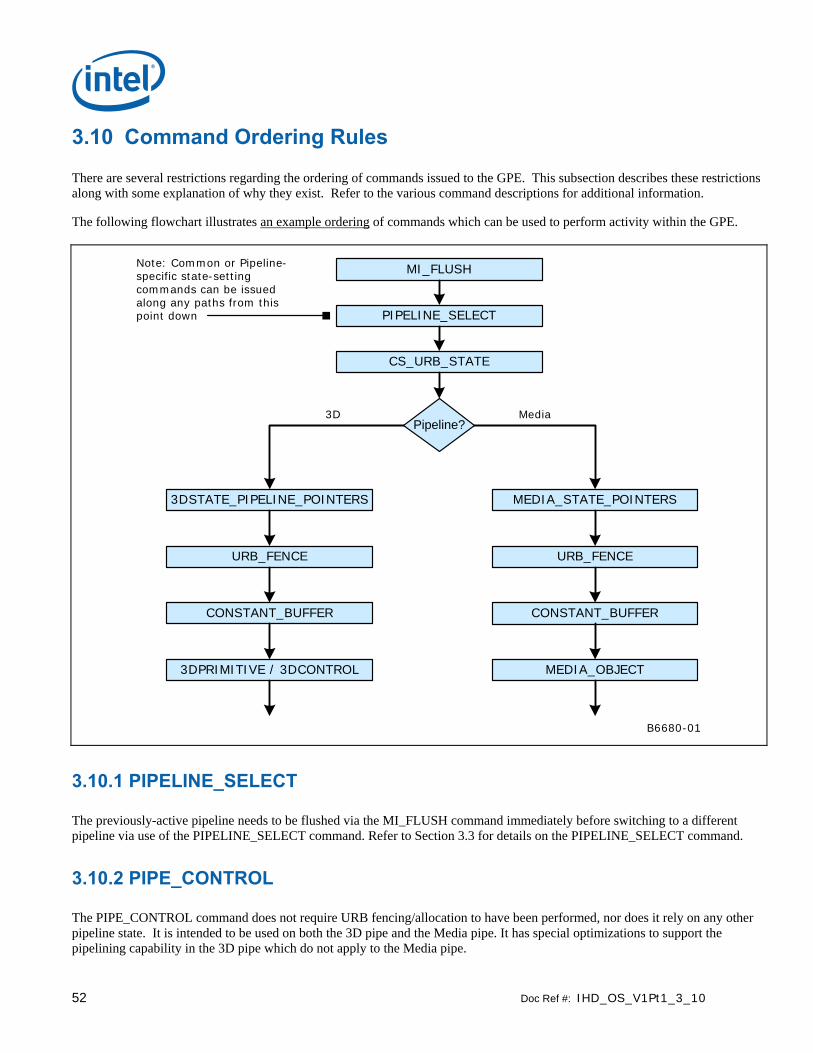
52 Doc Ref #: IHD_OS_V1Pt1_3_10
3.10 Command Ordering Rules
There are several restrictions regarding the ordering of commands issued to the GPE. This subsection describes these restrictions along with some explanation of why they exist. Refer to the various command descriptions for additional information.
The following flowchart illustrates an example ordering of commands which can be used to perform activity within the GPE.
B6680-01
MEDIA_STATE_POINTERS3DSTATE_PIPELINE_POINTERS
URB_FENCEURB_FENCE
CONSTANT_BUFFERCONSTANT_BUFFER
MEDIA_OBJECT3DPRIMITIVE / 3DCONTROL
MI_FLUSH
PIPELINE_SELECT
CS_URB_STATE
Pipeline?3D Media
Note: Common or Pipeline-specific state-setting commands can be issued along any paths from this point down
3.10.1 PIPELINE_SELECT
The previously-active pipeline needs to be flushed via the MI_FLUSH command immediately before switching to a different pipeline via use of the PIPELINE_SELECT command. Refer to Section 3.3 for details on the PIPELINE_SELECT command.
3.10.2 PIPE_CONTROL
The PIPE_CONTROL command does not require URB fencing/allocation to have been performed, nor does it rely on any other pipeline state. It is intended to be used on both the 3D pipe and the Media pipe. It has special optimizations to support the pipelining capability in the 3D pipe which do not apply to the Media pipe.

Doc Ref #: IHD_OS_V1Pt1_3_10 53
3.10.3 URB-Related State-Setting Commands
Several commands are used (among other things) to set state variables used in URB entry allocation --- specifically, the Number of URB Entries and the URB Entry Allocation Size state variables associated with various pipeline units. These state variables must be set-up prior to the issuing of a URB_FENCE command. (See the subsection on URB_FENCE below).
CS_URB_STATE (only) specifies these state variables for the common CS FF unit. 3DSTATE_PIPELINED_POINTERs sets the state variables for FF units in the 3D pipeline, and MEDIA_STATE_POINTERS sets them for the Media pipeline. Depending on which pipeline is currently active, only one of these commands needs to be used. Note that these commands can also be reissued at a later time to change other state variables, though if a change is made to (a) any Number of URB Entries and the URB Entry Allocation Size state variables or (b) the Maximum Number of Threads state for the GS or CLIP FF units, a URB_FENCE command must follow.
3.10.4 Common Pipeline State-Setting Commands
The following commands are used to set state common to both the 3D and Media pipelines. This state is comprised of CS FF unit state, non-pipelined global state (EU, etc.), and Sampler shared-function state.
• STATE_BASE_ADDRESS • STATE_SIP • 3DSTATE_SAMPLER_PALETTE_LOAD • 3DSTATE_CHROMA_KEY
The state variables associated with these commands must be set appropriately prior to initiating activity within a pipeline (i.e., 3DPRIMITIVE or MEDIA_OBJECT).

54 Doc Ref #: IHD_OS_V1Pt1_3_10
3.10.5 3D Pipeline-Specific State-Setting Commands
The following commands are used to set state specific to the 3D pipeline.
• 3DSTATE_PIPELINED_POINTERS • 3DSTATE_BINDING_TABLE_POINTERS • 3DSTATE_VERTEX_BUFFERS • 3DSTATE_VERTEX_ELEMENTS • 3DSTATE_INDEX_BUFFERS • 3DSTATE_VF_STATISTICS • 3DSTATE_DRAWING_RECTANGLE • 3DSTATE_CONSTANT_COLOR • 3DSTATE_DEPTH_BUFFER • 3DSTATE_POLY_STIPPLE_OFFSET • 3DSTATE_POLY_STIPPLE_PATTERN • 3DSTATE_LINE_STIPPLE • 3DSTATE_GLOBAL_DEPTH_OFFSET
The state variables associated with these commands must be set appropriately prior to issuing 3DPRIMITIVE.
3.10.6 Media Pipeline-Specific State-Setting Commands
The following commands are used to set state specific to the Media pipeline.
• MEDIA_STATE_POINTERS
The state variables associated with this command must be set appropriately prior to issuing MEDIA_OBJECT.

Doc Ref #: IHD_OS_V1Pt1_3_10 55
3.10.7 URB_FENCE (URB Fencing & Entry Allocation)
URB_FENCE command is used to initiate URB entry deallocation/allocation processes within pipeline FF units. The URB_FENCE command is first processed by the CS FF unit, and is then directed down the currently selected pipeline to the FF units comprising that pipeline.
As the FF units receive the URB_FENCE command, a URB entry deallocation/allocation process with be initiated if (a) the FF unit is currently enabled (note that some cannot be disabled) and (b) the ModifyEnable bit associated with that FF unit’s Fence value is set. If these conditions are met, the deallocation of the FF unit’s currently-allocated URB entries (if any) commences. (Implementation Note: For better performance, this deallocation proceeds in parallel with allocation of new handles).
Modifying the CS URB allocation via URB_FENCE invalidates any previous CURBE entries. Therefore software must subsequently [re]issue a CONSTANT_BUFFER command before CURBE data can be used in the pipeline.
The allocation of new handles (if any) for the FF unit then commences. The parameters used to perform this allocation come from (a) the URB_FENCE Fence values, and (b) the relevant URB entry state associated with the FF unit: specifically, the Number of URB Entries and the URB Entry Allocation Size. For the CS unit, this state is programmed via CS_URB_STATE, while the other FF units receive this state indirectly via PIPELINED_STATE_POINTERS or MEDIA_STATE_POINTERS commands.
Although a FF unit’s allocation process relies on it’s URB Fence as well as the relevant FF unit pipelined state, only the URB_FENCE command initiates URB entry deallocation/allocation. This imposes the following restriction: If a change is made to (a) the Number of URB Entries or URB Entry Allocation Size state for a given FF unit or (b) the Maximum Number of Threads state for the GS or CLIP FF units, a URB_FENCE command specifying a valid URB Fence state for that FF unit must be subsequently issued – at some point prior to the next CONSTANT_BUFFER, 3DPRIMITIVE (if using the 3D pipeline) or MEDIA_OBJECT (if using the Media pipeline). It is invalid to change Number of URB Entries or URB Entry Allocation Size state for an enabled FF units without also issuing a subsequent URB_FENCE command specifying a valid Fence valid for that FF unit.
It is valid to change a FF unit’s Fence value without specifying a change to its Number of URB Entries or URB Entry Allocation Size state, though the values must be self-consistent.

56 Doc Ref #: IHD_OS_V1Pt1_3_10
3.10.8 CONSTANT_BUFFER (CURBE Load)
The CONSTANT_BUFFER command is used to load constant data into the CURBE URB entries owned by the CS unit. In order to write into the URB, CS URB fencing and allocation must have been established. Therefore, CONSTANT_BUFFER can only be issued after CS_URB_STATE and URB_FENCE commands have been issued, and prior to any other pipeline processing (i.e., 3DPRIMITIVE or MEDIA_OBJECT). See the definition of CONSTANT_BUFFER for more details.
Modifying the CS URB allocation via URB_FENCE invalidates any previous CURBE entries. Therefore software must subsequently [re]issue a CONSTANT_BUFFER command before CURBE data can be used in the pipeline.
3.10.9 3DPRIMITIVE
Before issuing a 3DPRIMITIVE command, all state (with the exception of MEDIA_STATE_POINTERS) needs to be valid. Therefore the commands used to set this state need to have been issued at some point prior to the issue of 3DPRIMITIVE.
3.10.10 MEDIA_OBJECT
Before issuing a MEDIA_OBJECT command, all state (with the exception of 3D-pipeline-specific state) needs to be valid. Therefore the commands used to set this state need to have been issued at some point prior to the issue of MEDIA_OBJECT.
3.11 Video Command Streamer (VCS) VCS (Video Command Streamer) unit is primarily served as the software programming interface between the O/S driver and the MFD Engine. It is responsible for fetching, decoding, and dispatching of data packets (Media Commands with the header DW removed) to the front end interface module of Video Engine. Its logic functions include
• MMIO register programming interface. • DMA action for fetching of run lists and ring data from memory. • Management of the Head pointer for the Ring Buffer. • Decode of ring data and sending it to the appropriate destination • Handling of user interrupts and ring context switch interrupt. • Flushing the Video Engine • Handle NOP
The register programming (RM) bus is a dword interface bus that is driven by the Gx Command Streamer. The VCS unit will only claim memory mapped I/O cycles that are targeted to its range of 0x4000 to 0x4FFFF. The Gx and Video Engines use semaphore to synchronize their operations. Any interaction and control protocols between the VCS and Gx CS in IronLake will remain the same as in Cantiga. But in Gesher, VCS will operate completely independent of the Gx CS. The simple sequence of events is as follows: a ring (say PRB0) is programmed by a memory-mapped register write cycle. The DMA inside VCS is kicked off. The DMA fetches commands from memory based on the starting address and head pointer. The DMA requests cache lines from memory (one cacheline CL at a time). There is guaranteed space in the DMA FIFO (16 CL deep) for data coming back from memory. The DMA control logic has copies of the head pointer and the tail pointer. The DMA

Doc Ref #: IHD_OS_V1Pt1_3_10 57
increments the head pointer after making requests for ring commands. Once the DMA copy of the head pointer becomes equal to the tail pointer, the DMA stops requesting. The parser starts executing once the DMA FIFO has valid commands. All the commands have a header dword packet. Based on the encoding in the header packet, the command may be targeted towards AVC/VC1/MPEG2 engine or the command parser. After execution of every command, the actual head pointer is updated. The ring is considered empty when the head pointer becomes equal to the tail pointer.

58 Doc Ref #: IHD_OS_V1Pt1_3_10
4. Graphics Command Formats
4.1 Command Formats
This section describes the general format of the graphics device commands.
Graphics commands are defined with various formats. The first DWord of all commands is called the header DWord. The header contains the only field common to all commands -- the client field that determines the device unit that will process the command data. The Command Parser examines the client field of each command to condition the further processing of the command and route the command data accordingly.
Some Genx Devices include two Command Parsers, each controlling an independent processing engine. These will be referred to in this document as the Render Command Parser (RCP) and the Video Codec Command Parser (VCCP).
Valid client values for the Render Command Parser are:
Client # Client
0 Memory Interface (MI_xxx)
1 Miscellaneous (includes Trusted Ops)
2 2D Rendering (xxx_BLT_xxx)
3 Graphics Pipeline (3D and Media)
4-7 Reserved
Valid client values for the Video Codec Command Parser are:
Client # Client
0 Memory Interface (MI_xxx)
1-2 Reserved
3 AVC and VC1 State and Object Commands
4-7 Reserved
On [DevBW] and [DevCL], no Video Codec Command Parser is present.
Graphics commands vary in lenSNBh, though are always multiples of DWords. The lenSNBh of a command is either:
Implied by the client/opcode Fixed by the client/opcode yet included in a header field (so the Command Parser explicitly knows how much data to
copy/process) Variable, with a field in the header indicating the total lenSNBh of the command
Doc Ref #: IHD_OS_V1Pt1_3_10 59
Note that command sequences require QWord alignment and padding to QWord lenSNBh to be placed in Ring and Batch Buffers.
The following subsections provide a brief overview of the graphics commands by client type provides a diagram of the formats of the header DWords for all commands. Following that is a list of command mnemonics by client type.
4.1.1 Memor y Interface Commands Memory Interface (MI) commands are basically those commands which do not require processing by the 2D or 3D Rendering/Mapping engines. The functions performed by these commands include:
Control of the command stream (e.g., Batch Buffer commands, breakpoints, ARB On/Off, etc.)
Hardware synchronization (e.g., flush, wait-for-event) Software synchronization (e.g., Store DWORD, report head) Graphics buffer definition (e.g., Display buffer, Overlay buffer) Miscellaneous functions
Refer to the Memory Interface Commands chapter for a description of these commands.
4.1.2 2D Commands
The 2D commands include various flavors of Blt operations, along with commands to set up Blt engine state without actually performing a Blt. Most commands are of fixed lenSNBh, though there are a few commands that include a variable amount of "inline" data at the end of the command.
Refer to the 2D Commands chapter for a description of these commands.
4.1.3 3D/Media Commands
The 3D/Media commands are used to program the graphics pipelines for 3D or media operations.
Refer to the 3D chapter for a description of the 3D state and primitive commands and the Media chapter for a description of the media-related state and object commands.
4.1.4 Video Codec Commands
4.1.4.1 AVC Commands [DevCTG/DevILK]
The AVC commands are used to program the AVC Bit-Stream Serial Decoder attached to the Video Codec Command Parser. See the AVC BSD chapter for a description of these commands.
4.1.4.2 VC1 Commands [DevCTG/DevILK]
The VC1 commands are used to program the VC1 Bit-Stream Serial Decoder attached to the Video Codec Command Parser. See the VC1 BSD chapter for a description of these commands.

60 Doc Ref #: IHD_OS_V1Pt1_3_10
4.1.5 Command Header
Table 4-1. RCP Command Header Format
Bits
TYPE 31:29 28:24 23 22 21:0
Memory
Interface
(MI)
000 Opcode 00h – NOP 0Xh – Single DWord Commands 1Xh – Two+ DWord Commands 2Xh – Store Data Commands 3Xh – Ring/Batch Buffer Cmds
Identification No./DWord Count Command Dependent Data
5:0 – DWord Count 5:0 – DWord Count 5:0 – DWord Count
Reserved 001 Opcode – 11111 23:19 Sub Opcode 00h – 01h
18:16
Re-served
15:0
DWord Count
2D 010 Opcode Command Dependent Data 4:0 – DWord Count
TYPE 31:29 28:27 26:24 23:16 15:8 7:0
Common 011 00 Opcode – 000 Sub Opcode Data DWord Count
Common (NP) 011 00 Opcode – 001 Sub Opcode Data DWord Count
Reserved 011 00 Opcode – 010 – 111
Single Dword Command
011 01 Opcode – 000 – 001 Sub Opcode N/A
Reserved 011 01 Opcode – 010 – 111
Media State 011 10 Opcode – 000 Sub Opcode Dword Count
Media Object 011 10 Opcode – 001 – 010 Sub Opcode Dword Count
Reserved 011 10 Opcode – 011 – 111
3DState 011 11 Opcode – 000 Sub Opcode Data DWord Count
3DState (NP) 011 11 Opcode – 001 Sub Opcode Data DWord Count
PIPE_Control 011 11 Opcode – 010 Data DWord Count
3DPrimitive 011 11 Opcode – 011 Data DWord Count
Reserved 011 11 Opcode – 100 – 111
Reserved 1XX XX
NOTES:
The qualifier “NP” indicates that the state variable is non-pipelined and the render pipe is flushed before such a state variable is updated. The other state variables are pipelined (default).

Doc Ref #: IHD_OS_V1Pt1_3_10 61
4.2 Command Map This section provides a map of the graphics command opcodes.
4.2.1 Memory Interface Command Map All the following commands are defined in Memory Interface Commands.Table 4-2. Memory Interface Commands for RCP
Pipe Opcode (28:23)
Command
Render Video
[DevCTG+]
Blitter
1-DWord
00h MI_NOOP All All All 01h Reserved
02h MI_USER_INTERRUPT All All All 03h MI_WAIT_FOR_EVENT All All All 04h MI_FLUSH All All 05h MI_ARB_CHECK All All All 06h Reserved 07h MI_REPORT_HEAD All All All 08h MI_ARB_ON_OFF [DevCTG+] 09h Reserved 0Ah MI_BATCH_BUFFER_END All All All 0Bh MI_SUSPEND_FLUSH [DevILK]
0Fh Reserved
2+ DWord
10h Reserved 11h MI_OVERLAY_FLIP
Reserved [DevCTG+] [pre-DevCTG]
12h MI_LOAD_SCAN_LINES_INCL Reserved
All
13h MI_LOAD_SCAN_LINES_EXCL Reserved
All
14h MI_DISPLAY_BUFFER_INFO [DevBW], [DevCL] MI_DISPLAY_FLIP [DevCTG+]
All
15h Reserved 16h MI_SEMAPHORE_MBOX
[DevBW], [DevCL] Reserved [DevCTG+] All All
17h Reserved
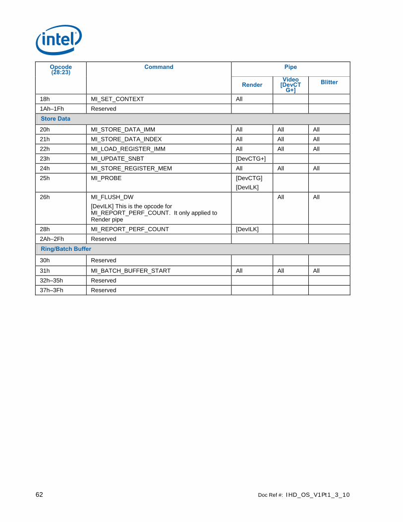
62 Doc Ref #: IHD_OS_V1Pt1_3_10
Pipe Opcode (28:23)
Command
Render Video
[DevCTG+]
Blitter
18h MI_SET_CONTEXT All 1Ah–1Fh Reserved
Store Data
20h MI_STORE_DATA_IMM All All All 21h MI_STORE_DATA_INDEX All All All 22h MI_LOAD_REGISTER_IMM All All All 23h MI_UPDATE_SNBT [DevCTG+] 24h MI_STORE_REGISTER_MEM All All All 25h MI_PROBE [DevCTG]
[DevILK]
26h MI_FLUSH_DW [DevILK] This is the opcode for MI_REPORT_PERF_COUNT. It only applied to Render pipe
All All
28h MI_REPORT_PERF_COUNT [DevILK] 2Ah–2Fh Reserved
Ring/Batch Buffer
30h Reserved
31h MI_BATCH_BUFFER_START All All All 32h–35h Reserved 37h–3Fh Reserved

Doc Ref #: IHD_OS_V1Pt1_3_10 63
4.2.2 2D Command Map
All the following commands are defined in Blitter Instructions.
Opcode (28:22) Command Comments
00h Reserved 01h XY_SETUP_BLT 02h Reserved 03h XY_SETUP_CLIP_BLT 04h–10h Reserved 11h XY_SETUP_MONO_PATTERN_SL_BLT 12h–23h Reserved 24h XY_PIXEL_BLT 25h XY_SCANLINES_BLT 26h XY_TEXT_BLT 23h–30h Reserved 31h XY_TEXT_IMMEDIATE_BLT 32h–3Fh Reserved 40h COLOR_BLT 41h–42h Reserved 43h SRC_COPY_BLT 44h–4Fh Reserved 50h XY_COLOR_BLT 51h XY_PAT_BLT 52h XY_MONO_PAT_BLT 53h XY_SRC_COPY_BLT 54h XY_MONO_SRC_COPY_BLT 55h XY_FULL_BLT 56h XY_FULL_MONO_SRC_BLT 57h XY_FULL_MONO_PATTERN_BLT 58h XY_FULL_MONO_PATTERN_MONO_SRC_BLT 59h XY_MONO_PAT_FIXED_BLT 5Ah–70h Reserved 71h XY_MONO_SRC_COPY_IMMEDIATE_BLT 72h XY_PAT_BLT_IMMEDIATE 73h XY_SRC_COPY_CHROMA_BLT 74h XY_FULL_IMMEDIATE_PATTERN_BLT 75h XY_FULL_MONO_SRC_IMMEDIATE_PATTERN_BLT 76h XY_PAT_CHROMA_BLT 77h XY_PAT_CHROMA_BLT_IMMEDIATE 78h–7Fh Reserved

64 Doc Ref #: IHD_OS_V1Pt1_3_10
4.2.3 3D/Media Command Map Pipeline
Type (28:27)
Opcode Sub Opcode
Command De finition Chapter
Common (pipelined)
Bits 26:24
Bits 23:16
0h 0h 00h URB_FENCE Graphics Processing Engine
0h 0h 01h CS_URB_STATE [Pre-DevSNB] Graphics Processing Engine
0h 0h 02h CONSTANT_BUFFER [Pre-DevSNB] Graphics Processing Engine
0h 0h 03h STATE_PREFETCH Graphics Processing Engine
0h 0h 04h-FFh Reserved
Common (non-
pipelined)
Bits 26:24
Bits 23:16
0h 1h 00h Reserved n/a
0h 1h 01h STATE_BASE_ADDRESS Graphics Processing Engine
0h 1h 02h STATE_SIP Graphics Processing Engine
0h 1h 04h–FFh Reserved n/a
Reserved Bits 26:24
Bits 23:16
0h 2h–7h XX Reserved n/a
Pipeline
Type (28:27)
Opcode Sub Opcode
Command De finition Chapter
Single DW Opcode (26:24)
Bits 23:16
1h 0h 00h-01h Reserved n/a
1h 0h 02h STATE_POINTER_INVALIDATE
[DevCTG+]
Graphics Processing Engine
1h 0h 03h-0Ah Reserved n/a
1h 0h 0Bh 3DSTATE_VF_STATISTICS Vertex Fetch
1h 0h 0Ch-FFh Reserved n/a
1h 1h 00h-03h Reserved n/a
1h 1h 04h PIPELINE_SELECT Graphics Processing Engine
1h 1h 05h-FFh Reserved n/a
1h 2h-7h XX Reserved n/a

Doc Ref #: IHD_OS_V1Pt1_3_10 65
Media Opcode (26:24)
Bits 23:16
2h 0h 00h MEDIA_STATE_POINTERS Media
2h 0h 05h-FFh Reserved n/a
2h 1h 00h MEDIA_OBJECT Media
2h 1h 01h MEDIA_OBJECT_EX Media
2h 1h 02h MEDIA_OBJECT_PRT Media
2h 1h 04h-FFh Reserved n/a
2h 2h–7h XX Reserved n/a
Pipeline Type
(28:27)
Opcode Sub Opcode
Command De finition Chapter
3D State (Pipelined
)
Bits 26:24
Bits 23:16
3h 0h 00h 3DSTATE_PIPELINED_POINTERS 3D Pipeline
3h 0h 03h Reserved n/a
3h 0h 05h Reserved 3D Pipeline
3h 0h 08h 3DSTATE_VERTEX_BUFFERS Vertex Fetch
3h 0h 09h 3DSTATE_VERTEX_ELEMENTS Vertex Fetch
3h 0h 0Ah 3DSTATE_INDEX_BUFFER Vertex Fetch
3h 0h 0Bh 3DSTATE_VF_STATISTICS Vertex Fetch
3h 0h 0Ch Reserved n/a
3h 0h 11h 3DSTATE_GS [DevSNB+] Geometry Shader
3h 0h 12h 3DSTATE_CLIP [DevSNB+] Clipper
3h 0h 13h 3DSTATE_SF [DevSNB+] Strips & Fans
3h 0h 14h 3DSTATE_WM [DevSNB+] Windower
3D State (Non-
Pipelined)
Bits 26:24
Bits 23:16
3h 1h 00h 3DSTATE_DRAWING_RECTANGLE Strips & Fans
3h 1h 01h 3DSTATE_CONSTANT_COLOR Color Calculator
3h 1h 02h 3DSTATE_SAMPLER_PALETTE_LOAD0 Sampling Engine
3h 1h 03h Reserved
3h 1h 04h 3DSTATE_CHROMA_KEY Sampling Engine

66 Doc Ref #: IHD_OS_V1Pt1_3_10
Pipeline Type
(28:27)
Opcode Sub Opcode
Command De finition Chapter
3h 1h 05h 3DSTATE_DEPTH_BUFFER Windower
3h 1h 06h 3DSTATE_POLY_STIPPLE_OFFSET Windower
3h 1h 07h 3DSTATE_POLY_STIPPLE_PATTERN Windower
3h 1h 08h 3DSTATE_LINE_STIPPLE Windower
3h 1h 09h 3DSTATE_GLOBAL_DEPTH_OFFSET_CLAMP Windower
3h 1h 0Ah [DevCTG]: 3DSTATE_AA_LINE_PARAMS [DevCTG+]
Windower
3h 1h 0Bh 3DSTATE_GS_SVB_INDEX [DevCTG+] Geometry Shader
3h 1h 0Ch 3DSTATE_SAMPLER_PALETTE_LOAD1 [DevCTG-B+]
Sampling Engine
3h 1h 0Eh 3DSTATE_STENCIL_BUFFER [DevILK]
Reserved [ILK,
Windower
3h 1h 0Fh 3DSTATE_HIER_DEPTH_BUFFER [ILK,
Reserved [ILK,]
Windower
3h 1h 10h 3DSTATE_CLEAR_PARAMS [ILK, Windower
3h 1h 11h 3DSTATE_MONOFILTER_SIZE [ILK] Sampling Engine
3h 1h 17h 3DSTATE_SO_DECL_LIST HW Streamout
3h 1h 18h 3DSTATE_SO_BUFFER HW Streamout
3h 1h 19h–FFh Reserved n/a
3D (Control)
Bits 26:24
Bits 23:16
3h 2h 00h PIPE_CONTROL 3D Pipeline
3h 2h 01h–FFh Reserved n/a
3D (Primitive)
Bits 26:24
Bits 23:16
3h 3h 00h 3DPRIMITIVE Vertex Fetch
3h 3h 01h–FFh Reserved n/a
3h 4h–7h 00h–FFh Reserved n/a

Doc Ref #: IHD_OS_V1Pt1_3_10 67
4.2.4 Video Codec Command Map
4.2.4.1 AVC BSD Command Map [DevCTG/DevILK]
This map is N/A to [DevBW], [DevCL]
Table 4-3. AVC Commands for the VCCP
Pipeline Type (28:27)
Opcode (26:24)
Sub Opcode (23:16)
Command De finition Chapter
AVC State
2h 4h 0h AVC_BSD_IMG_STATE AVC BSD
2h 4h 1h AVC_BSD_QM_STATE AVC BSD
2h 4h 2h AVC_BSD_SLICE_STATE AVC BSD
2h 4h 3h AVC_BSD_BUF_BASE_STATE AVC BSD
2h 4h 4h BSD_IND_OBJ_BASE_ADDR AVC BSD
2h 4h 5h-7h Reserved n/a
AVC Object
2h 4h 8h AVC_BSD_OBJECT AVC BSD
2h 4h 9h-FFh Reserved n/a
4.2.4.2 VC1 BSD Command Map [DevCTG/DevILK]
This map is N/A to [DevBW], [DevCL].
Pipeline Type (28:27)
Opcode (26:24)
Sub Opcode (23:16)
Command De finition Chapter
VC1 State
2h 5h 0h VC1_BSD_PIC_STATE VC1 BSD
2h 5h 1h Reserved n/a
2h 5h 2h Reserved n/a
2h 5h 3h VC1_BSD_BUF_BASE_STATE VC1 BSD
2h 5h 4h Reserved n/a
2h 5h 5h-7h Reserved n/a

68 Doc Ref #: IHD_OS_V1Pt1_3_10
VC1 Object
2h 5h 8h VC1_BSD_OBJECT VC1 BSD
2h 5h 9h-FFh Reserved n/a

Doc Ref #: IHD_OS_V1Pt1_3_10 69
5. Register Address Maps
5.1 Graphics Register Address Map
This chapter provides address maps of the graphics controllers I/O and memory-mapped registers. Individual register bit field descriptions are provided in the following chapters. PCI configuration address maps and register bit descriptions are provided in the following chapter.
5.1.1 Memory and I/O Space Registers
This section provides a high-level register map (register groupings per function). The memory and I/O maps for the graphics device registers are shown in the following table, except PCI Configuration registers that are described in the following chapter.
NOTE: The VGA and Extended VGA registers can be accessed via standard VGA I/O locations as well as via memory-mapped locations.
NOTE: All graphics MMIO registers can also be accessed via CPU I/O. See IOBASE, MMIO_INDEX and MMIO_DATA I/O registers in the MontaraGM Cspec.
The memory space address listed for each register is an offset from the base memory address programmed into the MMADR register (PCI configuration offset 14h).
Table 5-1. Graphics Controller Register Memory and I/O Map
Start Offset
End Offset
Description
00000h 00FFFh VGA and Extended VGA Control Registers. These registers are located in both I/O space and memory space. The VGA and Extended VGA registers contain the following register sets: General Control/Status, Sequencer (SRxx), Graphics Controller (GRxx), Attribute Controller (Arxx), VGA Color Palette, and CRT Controller (CRxx) registers. Detailed bit descriptions are provided in the VGA and Extended VGA Register Chapter. The registers within a set are accessed using an indirect addressing mechanism as described at the beginning of each section. Note that some of the register description sections have additional operational information at the beginning of the section
01000h 01FFFh Reserved

70 Doc Ref #: IHD_OS_V1Pt1_3_10
Start Offset
End Offset
Description
02000h 02FFFh Instruction, Memory, and Interrupt Control Registers: Instruction Control Registers Ring Buffer registers and page table control registers are located in this address range. Various instruction status, error, and operating registers are located in this group of registers. Graphics Memory Fence Registers. The Graphics Memory Fence registers are used for memory tiling capabilities. Interrupt Control/Status Registers. This register set provides interrupt control/status for various GC functions. Display Interface Control Register. This register controls the FIFO watermark and provides burst lenSNBh control. Logical Context Registers Pipeline Statistic Counters
03000h 031FFh FENCE & Per Process SNBT Control registers
03200h 03FFFh Frame Buffer Compression Registers
04000h 043FFh Instruction Control Registers for Secondary (BSD) Command Streamer.
On [DevBW] and [DevCL] this range is Reserved.
04400h 04FFFh Video Decode Fixed Function Control Registers.
On [DevBW] and [DevCL] this range is Reserved.
05000h 05FFFh I/O Control Registers
06000h 06FFFh Clock Control Registers. This memory address space is the location of the GC clock control and power management registers
09000h 09FFFh Reserved
0A000h 0AFFFh Display Palette Registers
0B000h 0FFFFh Reserved
10000h 13FFFh MMIO MCHBAR. Alias through which the graphics driver can access registers in the MCHBAR accessed through device 0.
14000h 2FFFFh Reserved
30000h 3FFFFh Overlay Registers. These registers provide control of the overlay engine. The overlay registers are double-buffered with one register buffer located in graphics memory and the other on the device. On-chip registers are not directly writeable. To update the on-chip registers software writes to the register buffer area in graphics memory and instructs the device to update the on-chip registers.
40000h 5FFFFh Reserved
60000h 6FFFFh Display Engine Pipeline Registers
70000h 72FFFh Display and Cursor Registers
73000h 73FFFh Performance Counters
74000h 7FFFFh Reserved

Doc Ref #: IHD_OS_V1Pt1_3_10 71
5.1.2 PCI Configuration Space
See the releveant EDS/C-Specs for details on accessing PCI configuration space, PCI address map tables, and register descriptions.
5.1.3 Graphics Register Memory Address Map
All graphics device registers are directly accessible via memory-mapped I/O and indirectly accessible via the MMIO_INDEX and MMIO_DATA I/O registers. In addition, the VGA and Extended VGA registers are I/O mapped.
5.2 VGA and Extended VGA Register Map
For I/O locations, the value in the address column represents the register I/O address. For memory mapped locations, this address is an offset from the base address programmed in the MMADR register.
5.2.1 VGA and Extended VGA I/O and Memory Register Map Table 5-2. I/O and Memory Register Map
Address Register Name (Read) Register Name (Write)
2D Registers
3B0h–3B3h Reserved Reserved
3B4h VGA CRTC Index (CRX) (monochrome)
VGA CRTC Index (CRX) (monochrome)
3B5h VGA CRTC Data (monochrome) VGA CRTC Data (monochrome)
3B6h–3B9h Reserved Reserved
3Bah VGA Status Register (ST01) VGA Feature Control Register (FCR)
3BBh–3BFh Reserved Reserved
3C0h VGA Attribute Controller Index (ARX) VGA Attribute Controller Index (ARX)/ VGA Attribute Controller Data (alternating writes select ARX or write ARxx Data)
3C1h VGA Attribute Controller Data (read ARxx data)
Reserved
3C2h VGA Feature Read Register (ST00) VGA Miscellaneous Output Register (MSR)
3C3h Reserved Reserved
3C4h VGA Sequencer Index (SRX) VGA Sequencer Index (SRX)
3C5h VGA Sequencer Data (SRxx) VGA Sequencer Data (SRxx)
3C6h VGA Color Palette Mask (DACMASK) VGA Color Palette Mask (DACMASK)
3C7h VGA Color Palette State (DACSTATE)
VGA Color Palette Read Mode Index (DACRX)

72 Doc Ref #: IHD_OS_V1Pt1_3_10
Address Register Name (Read) Register Name (Write)
3C8h VGA Color Palette Write Mode Index (DACWX)
VGA Color Palette Write Mode Index (DACWX)
3C9h VGA Color Palette Data (DACDATA) VGA Color Palette Data (DACDATA)
3CAh VGA Feature Control Register (FCR) Reserved
3CBh Reserved Reserved
3CCh VGA Miscellaneous Output Register (MSR)
Reserved
3CDh Reserved Reserved
3CEh VGA Graphics Controller Index (GRX) VGA Graphics Controller Index (GRX)
3CFh VGA Graphics Controller Data (GRxx) VGA Graphics Controller Data (GRxx)
3D0h–3D1h Reserved Reserved
2D Registers
3D4h VGA CRTC Index (CRX) VGA CRTC Index (CRX)
3D5h VGA CRTC Data (CRxx) VGA CRTC Data (CRxx)
System Configuration Registers
3D6h GFX/2D Configurations Extensions Index (XRX)
GFX/2D Configurations Extensions Index (XRX)
3D7h GFX/2D Configurations Extensions Data (XRxx)
GFX/2D Configurations Extensions Data (XRxx)
2D Registers
3D8h–3D9h Reserved Reserved
3DAh VGA Status Register (ST01) VGA Feature Control Register (FCR)
3DBh–3DFh Reserved Reserved

Doc Ref #: IHD_OS_V1Pt1_3_10 73
5.3 Indirect VGA and Extended VGA Register Indices
The registers listed in this section are indirectly accessed by programming an index value into the appropriate SRX, GRX, ARX, or CRX register. The index and data register address locations are listed in the previous section. Additional details concerning the indirect access mechanism are provided in the VGA and Extended VGA Register Description Chapter (see SRxx, GRxx, ARxx or CRxx sections).
Table 5-3. 2D Sequence Registers (3C4h / 3C5h)
Index Sy m Description
00h SR00 Sequencer Reset
01h SR01 Clocking Mode
02h SR02 Plane / Map Mask
03h SR03 Character Font
04h SR04 Memory Mode
07h SR07 Horizontal Character Counter Reset

74 Doc Ref #: IHD_OS_V1Pt1_3_10
Table 5-4. 2D Graphics Controller Registers (3CEh / 3CFh)
Index Sym Register Name
00h GR00 Set / Reset 01h GR01 Enable Set / Reset 02h GR02 Color Compare 03h GR03 Data Rotate 04h GR04 Read Plane Select 05h GR05 Graphics Mode 06h GR06 Miscellaneous 07h GR07 Color Don’t Care 08h GR08 Bit Mask 10h GR10 Address Mapping 11h GR11 Page Selector 18h GR18 Software Flags
Table 5-5. 2D Attribute Controller Registers (3C0h / 3C1h)
Index Sym Register Name
00h AR00 Palette Register 0
01h AR01 Palette Register 1
02h AR02 Palette Register 2
03h AR03 Palette Register 3
04h AR04 Palette Register 4
05h AR05 Palette Register 5
06h AR06 Palette Register 6
07h AR07 Palette Register 7
08h AR08 Palette Register 8
09h AR09 Palette Register 9
0Ah AR0A Palette Register A
0Bh AR0B Palette Register B
0Ch AR0C Palette Register C
0Dh AR0D Palette Register D
0Eh AR0E Palette Register E
0Fh AR0F Palette Register F
10h AR10 Mode Control
11h AR11 Color
12h AR12 Memory Plane Enable
13h AR13 Horizontal Pixel Panning
14h AR14 Color Select

Doc Ref #: IHD_OS_V1Pt1_3_10 75
Table 5-6. 2D CRT Controller Registers (3B4h / 3D4h / 3B5h / 3D5h)
Index Sym Register Name
00h CR00 Horizontal Total
01h CR01 Horizontal Display Enable End
02h CR02 Horizontal Blanking Start
03h CR03 Horizontal Blanking End
04h CR04 Horizontal Sync Start
05h CR05 Horizontal Sync End
06h CR06 Vertical Total
07h CR07 Overflow
08h CR08 Preset Row Scan
09h CR09 Maximum Scan Line
0Ah CR0A Text Cursor Start
0Bh CR0B Text Cursor End
0Ch CR0C Start Address High
0Dh CR0D Start Address Low
0Eh CR0E Text Cursor Location High
0Fh CR0F Text Cursor Location Low
10h CR10 Vertical Sync Start
11h CR11 Vertical Sync End
12h CR12 Vertical Display Enable End
13h CR13 Offset
14h CR14 Underline Location
15h CR15 Vertical Blanking Start
16h CR16 Vertical Blanking End
17h CR17 CRT Mode
18h CR18 Line Compare
22h CR22 Memory Read Latch Data
24h CR24 Test Register for Toggle State of Attribute Control Register

76 Doc Ref #: IHD_OS_V1Pt1_3_10
6. Memory Data Formats This chapter describes the attributes associated with the memory-resident data objects operated on by the graphics pipeline. This includes object types, pixel formats, memory layouts, and rules/restrictions placed on the dimensions, physical memory location, pitch, alignment, etc. with respect to the specific operations performed on the objects.
6.1 Memory Object Overview
Any memory data accessed by the device is considered part of a memory object of some memory object type.
6.1.1 Memor y Object Types
The following table lists the various memory objects types and an indication of their role in the system.
Memory Object Type Role
Graphics Translation Table (SNBT) Contains PTEs used to translate “graphics addresses” into physical memory addresses.
Hardware Status Page Cached page of sysmem used to provide fast driver synchronization.
Logical Context Buffer Memory areas used to store (save/restore) images of hardware rendering contexts. Logical contexts are referenced via a pointer to the corresponding Logical Context Buffer.
Ring Buffers Buffers used to transfer (DMA) instruction data to the device. Primary means of controlling rendering operations.
Batch Buffers Buffers of instructions invoked indirectly from Ring Buffers.
State Descriptors Contains state information in a prescribed layout format to be read by hardware. Many different state descriptor formats are supported.
Vertex Buffers Buffers of 3D vertex data indirectly referenced through “indexed” 3D primitive instructions.
VGA Buffer
(Must be mapped UC on PCI)
Graphics memory buffer used to drive the display output while in legacy VGA mode.
Display Surface Memory buffer used to display images on display devices.
Overlay Surface Memory buffer used to display overlaid images on display devices.
Overlay Register, Filter Coefficients
Buffer
Memory area used to provide double-buffer for Overlay register and filter coefficient loading.
Cursor Surface Hardware cursor pattern in memory.
2D Render Source Surface used as primary input to 2D rendering operations.

Doc Ref #: IHD_OS_V1Pt1_3_10 77
Memory Object Type Role
2D Render R-M-W Destination 2D rendering output surface that is read in order to be combined in the rendering function. Destination surfaces that accessed via this Read-Modify-Write mode have somewhat different restrictions than Write-Only Destination surfaces.
2D Render Write-Only Destination 2D rendering output surface that is written but not read by the 2D rendering function. Destination surfaces that accessed via a Write-Only mode have somewhat different restrictions than Read-Modify-Write Destination surfaces.
2D Monochrome Source 1 bpp surfaces used as inputs to 2D rendering after being converted to foreground/background colors.
2D Color Pattern 8x8 pixel array used to supply the “pattern” input to 2D rendering functions.
DIB “Device Independent Bitmap” surface containing “logical” pixel values that are converted (via LUTs) to physical colors.
3D Color Buffer Surface receiving color output of 3D rendering operations. May also be accessed via R-M-W (aka blending). Also referred to as a Render Target.
3D Depth Buffer Surface used to hold per-pixel depth and stencil values used in 3D rendering operations. Accessed via RMW.
3D Texture Map Color surface (or collection of surfaces) which provide texture data in 3D rendering operations.
“Non-3D” Texture
Surface read by Texture Samplers, though not in normal 3D rendering operations (e.g., in video color conversion functions).
Motion Comp Surfaces These are the Motion Comp reference pictures.
Motion Comp Correction Data Buffer This is Motion Comp intra-coded or inter-coded correction data.
6.2 Channel Formats
6.2.1 Unsigned Normalized (UNORM)
An unsigned normalized value with n bits is interpreted as a value between 0.0 and 1.0. The minimum value (all 0’s) is interpreted as 0.0, the maximum value (all 1’s) is interpreted as 1.0. Values in between are equally spaced. For example, a 2-bit UNORM value would have the four values 0, 1/3, 2/3, and 1.
If the incoming value is interpreted as an n-bit integer, the interpreted value can be calculated by dividing the integer by 2n-1.
6.2.2 Gamma Conversion (SRGB)
Gamma conversion is only supported on UNORM formats. If this flag is included in the surface format name, it indicates that a reverse gamma conversion is to be done after the source surface is read, and a forward gamma conversion is to be done before the destination surface is written.

78 Doc Ref #: IHD_OS_V1Pt1_3_10
6.2.3 Signed Normalized (SNORM)
A signed normalized value with n bits is interpreted as a value between -1.0 and +1.0. If the incoming value is interpreted as a 2’s-complement n-bit signed integer, the interpreted value can be calculated by dividing the integer by 2n-1-1. Note that the most negative value of -2n-1 will result in a value slightly smaller than -1.0. This value is clamped to -1.0, thus there are two representations of -1.0 in SNORM format.
6.2.4 Unsigned Integer (UINT/USCALED)
The UINT and USCALED formats interpret the source as an unsigned integer value with n bits with a range of 0 to 2n-1.
The UINT formats copy the source value to the destination (zero-extending if required), keeping the value as an integer.
The USCALED formats convert the integer into the corresponding floating point value (e.g., 0x03 --> 3.0f). For 32-bit sources, the value is rounded to nearest even.
6.2.5 Signed Integer (SINT/SSCALED)
A signed integer value with n bits is interpreted as a 2’s complement integer with a range of -2n-1 to +2n-1-1.
The SINT formats copy the source value to the destination (sign-extending if required), keeping the value as an integer.
The SSCALED formats convert the integer into the corresponding floating point value (e.g., 0xFFFD --> -3.0f). For 32-bit sources, the value is rounded to nearest even.
6.2.6 Floating Point (FLOAT)
Refer to IEEE Standard 754 for Binary Floating-Point Arithmetic. The IA-32 Intel (R) Architecture Software Developer’s Manual also describes floating point data types (though GENX deviates slightly from those behaviors).
6.2.6.1 32-bit Floating Point
Bit De scription
31 Sign (s)
30:23 Exponent (e) Biased Exponent
22:0 Fraction (f) Does not include “hidden one”
The value of this data type is derived as: • if e == 255 and f != 0, then v is NaN regardless of s • if e == 255 and f == 0, then v = (-1)s*infinity (signed infinity) • if 0 < e < 255, then v = (-1)s*2(e-127)*(1.f) • if e == 0 and f != 0, then v = (-1)s*2(e-126)*(0.f) (denormalized numbers) • if e == 0 and f == 0, then v = (-1)s*0 (signed zero)

Doc Ref #: IHD_OS_V1Pt1_3_10 79
6.2.6.2 64-bit Floating Point
Bit De scription
63 Sign (s)
62:52 Exponent (e) Biased Exponent
51:0 Fraction (f) Does not include “hidden one”
The value of this data type is derived as: • if e == b’11..11’ and f != 0, then v is NaN regardless of s • if e == b’11..11’ and f == 0, then v = (-1)s*infinity (signed infinity) • if 0 < e < b’11..11’, then v = (-1)s*2(e-1023)*(1.f) • if e == 0 and f != 0, then v = (-1)s*2(e-1022)*(0.f) (denormalized numbers) • if e == 0 and f == 0, then v = (-1)s*0 (signed zero)
6.2.6.3 16-bit Floating Point
Bit De scription
15 Sign (s)
14:10 Exponent (e) Biased Exponent
9:0 Fraction (f) Does not include “hidden one”
The value of this data type is derived as: • if e == 31 and f != 0, then v is NaN regardless of s • if e == 31 and f == 0, then v = (-1)s*infinity (signed infinity) • if 0 < e < 31, then v = (-1)s*2(e-15)*(1.f) • if e == 0 and f != 0, then v = (-1)s*2(e-14)*(0.f) (denormalized numbers) • if e == 0 and f == 0, then v = (-1)s*0 (signed zero)

80 Doc Ref #: IHD_OS_V1Pt1_3_10
The following table represents relationship between 32 bit and 16 bit floating point ranges:
flt32
exponent Unbiased exponent flt16
exponent flt16 fraction 255 254 127 ...
127+16 16 Infinity 31 1.1111111111 127+15 15 Max exponent 30 1.xxxxxxxxxx
127 0 15 1.xxxxxxxxxx 113 -14 Min exponent 1 1.xxxxxxxxxx 112 Denormalized 0 0.1xxxxxxxxx 111 Denormalized 0 0.01xxxxxxxx 110 Denormalized 0 0.001xxxxxxx 109 Denormalized 0 0.0001xxxxxx 108 Denormalized 0 0.00001xxxxx 107 Denormalized 0 0.000001xxxx 106 Denormalized 0 0.0000001xxx 115 Denormalized 0 0.00000001xx 114 Denormalized 0 0.000000001x 113 Denormalized 0 0.0000000001 112 Denormalized 0 0.0 ... 0 0 0.0
Conversion from the 32-bit floating point format to the 16-bit format should be done with round to nearest even.
6.2.6.4 11-bit Floating Point
Bit De scription
10:6 Exponent (e) Biased Exponent
5:0 Fraction (f) Does not include “hidden one”
The value of this data type is derived as: • if e == 31 and f != 0 then v = NaN • if e == 31 and f == 0 then v = +infinity • if 0 < e < 31, then v = 2(e-15)*(1.f) • if e == 0 and f != 0, then v = 2(e-14)*(0.f) (denormalized numbers) • if e == 0 and f == 0, then v = 0 (zero)

Doc Ref #: IHD_OS_V1Pt1_3_10 81
6.2.6.5 10-bit Floating Point
Bit De scription
9:5 Exponent (e) Biased Exponent
4:0 Fraction (f) Does not include “hidden one”
The value of this data type is derived as: • if e == 31 and f != 0 then v = NaN • if e == 31 and f == 0 then v = +infinity • if 0 < e < 31, then v = 2(e-15)*(1.f) • if e == 0 and f != 0, then v = 2(e-14)*(0.f) (denormalized numbers) • if e == 0 and f == 0, then v = 0 (zero)
6.2.6.6 Shared Exponent
The R9G9B9E5_SHAREDEXP format contains three channels that share an exponent. The three fractions assume an impled “0” rather than an implied “1” as in the other floating point formats. This format does not support infinity and NaN values. There are no sign bits, only positive numbers and zero can be represented. The value of each channel is determined as follows, where “f” is the fraction of the corresponding channel, and “e” is the shared exponent.
v = (0.f)*2(e-15)
Bit De scription
31:27 Exponent (e) Biased Exponent
26:18 Blue Fraction
17:9 Green Fraction
8:0 Red Fraction
6.3 Non-Video Surface Formats
This section describes the lowest-level organization of a surfaces containing discrete “pixel” oriented data (e.g., discrete pixel (RGB,YUV) colors, subsampled video data, 3D depth/stencil buffer pixel formats, bump map values etc. Many of these pixel formats are common to the various pixel-oriented memory object types.

82 Doc Ref #: IHD_OS_V1Pt1_3_10
6.3.1 Surface Format Naming
Unless indicated otherwise, all pixels are stored in “little endian” byte order. I.e., pixel bits 7:0 are stored in byte n, pixel bits 15:8 are stored in byte n+1, and so on. The format labels include color components in little endian order (e.g., R8G8B8A8 format is physically stored as R, G, B, A).
The name of most of the surface formats specifies its format. Channels are listed in little endian order (LSB channel on the left, MSB channel on the right), with the channel format specified following the channels with that format. For example, R5G5_SNORM_B6_UNORM contains, from LSB to MSB, 5 bits of red in SNORM format, 5 bits of green in SNORM format, and 6 bits of blue in UNORM format.
6.3.2 Intensity Formats
All surface formats containing “I” include an intensity value. When used as a source surface for the sampling engine, the intensity value is replicated to all four channels (R,G,B,A) before being filtered. Intensity surfaces are not supported as destinations.
6.3.3 Luminance Formats
All surface formats contaning “L” include a luminance value. When used as a source surface for the sampling engine, the luminance value is replicated to the three color channels (R,G,B) before being filtered. The alpha channel is provided either from another field or receives a default value. Luminance surfaces are not supported as destinations.
6.3.4 R1_UNORM (same as R1_UINT) and MONO8
When used as a texel format, the R1_UNORM format contains 8 1-bit Intensity (I) values that are replicated to all color channels. Note that T0 of byte 0 of a R1_UNORM-formatted texture corresponds to Texel[0,0]. This is different from the format used for monochrome sources in the Blt engine.
7 6 5 4 3 2 1 0
T7 T6 T5 T4 T3 T2 T1 T0
Bit De scription
T0 Texel 0 On texture reads, this (unsigned) 1-bit value is replicated to all color channels. Format: U1
... ...
T7 Texel 7 On texture reads, this (unsigned) 1-bit value is replicated to all color channels. Format: U1

Doc Ref #: IHD_OS_V1Pt1_3_10 83
MONO8 format is identical to R1_UNORM but has different semantics for filtering. MONO8 is the only supported format for the MAPFILTER_MONO filter. See the Sampling Engine chapter.
6.3.5 Palette Formats
6.3.5.1 P4A4_UNORM
This surface format contains a 4-bit Alpha value (in the high nibble) and a 4-bit Palette Index value (in the low nibble).
7 4 3 0
Alpha Palette Index
Bit De scription
7:4 Alpha Alpha value which will be replicated to both the high and low nibble of an 8-bit value, and then divided by 255 to yield a [0.0,1.0] Alpha value. Format: U4
3:0 Palette Index
A 4-bit index which is used to lookup a 24-bit (RGB) value in the texture palette (loaded via 3DSTATE_SAMPLER_PALETTE_LOADx)
Format: U4
6.3.5.2 A4P4_UNORM
This surface format contains a 4-bit Alpha value (in the low nibble) and a 4-bit Color Index value (in the high nibble).
7 4 3 0
Palette Index Alpha
Bit De scription
7:4 Palette Index
A 4-bit color index which is used to lookup a 24-bit RGB value in the texture palette.
Format: U4
3:0 Alpha Alpha value which will be replicated to both the high and low nibble of an 8-bit value, and then divided by 255 to yield a [0.0,1.0] alpha value. Format: U4

84 Doc Ref #: IHD_OS_V1Pt1_3_10
6.3.5.3 P8A8_UNORM
This surface format contains an 8-bit Alpha value (in the high byte) and an 8-bit Palette Index value (in the low byte).
15 8 7 0
Alpha Palette Index
Bit De scription
7:4 Alpha Alpha value which will be divided by 255 to yield a [0.0,1.0] Alpha value. Format: U8
3:0 Palette Index
An 8-bit index which is used to lookup a 24-bit (RGB) value in the texture palette (loaded via 3DSTATE_SAMPLER_PALETTE_LOADx)
Format: U8
6.3.5.4 A8P8_UNORM
This surface format contains an 8-bit Alpha value (in the low byte) and an 8-bit Color Index value (in the high byte).
15 8 7 0
Palette Index Alpha
Bit De scription
15:8 Palette Index
An 8-bit color index which is used to lookup a 24-bit RGB value in the texture palette.
Format: U8
7:0 Alpha Alpha value which will be divided by 255 to yield a [0.0,1.0] alpha value. Format: U8

Doc Ref #: IHD_OS_V1Pt1_3_10 85
6.3.5.5 P8_UNORM
This surface format contains only an 8-bit Color Index value.
Bit De scription
7:0 Palette Index
An 8-bit color index which is used to lookup a 32-bit ARGB value in the texture palette.
Format: U8
6.3.5.6 P2_UNORM
This surface format contains only a 2-bit Color Index value.
Bit De scription
1:0 Palette Index
A 2-bit color index which is used to lookup a 32-bit ARGB value in the texture palette.
Format: U2

86 Doc Ref #: IHD_OS_V1Pt1_3_10
6.4 Compressed Surface Formats
This section contains information on the internal organization of compressed surface formats.
6.4.1 FXT Texture Formats
There are four different FXT1 compressed texture formats. Each of the formats compress two 4x4 texel blocks into 128 bits. In each compression format, the 32 texels in the two 4x4 blocks are arranged according to the following diagram:
Figure 6-1. FXT1 Encoded Blocks
B6682-01
t16 t17 t18 t19
t20 t21 t22 t23
t24 t25 t26 t27
t28 t29 t30 t31
t0 t1 t2 t3
t4 t5 t6 t7
t8 t9 t10 t11
t12 t13 t14 t15
6.4.1.1 Overview of FXT1 Formats
During the compression phase, the encoder selects one of the four formats for each block based on which encoding scheme results in best overall visual quality. The following table lists the four different modes and their encodings:
Table 6-1. FXT1 Format Summary
Bit 127
Bit 126
Bit 125
Block Compression
Mode
Summary Description
0 0 X CC_HI 2 R5G5B5 colors supplied. Single LUT with 7 interpolated color values and transparent black
0 1 0 CC_CHROMA 4 R5G5B5 colors used directly as 4-entry LUT.
0 1 1 CC_ALPHA 3 A5R5G5B5 colors supplied. LERP bit selects between 1 LUT with 3 discrete colors + transparent black and 2 LUTs using interpolated values of Color 0,1 (t0-15) and Color 1,2 (t16-31).
1 x x CC_MIXED 4 R5G5B5 colors supplied, where Color0,1 LUT is used for t0-t15, and Color2,3 LUT used for t16-31. Alpha bit selects between LUTs with 4 interpolated colors or 3 interpolated colors + transparent black.

Doc Ref #: IHD_OS_V1Pt1_3_10 87
6.4.1.2 FXT1 CC_HI Format
In the CC_HI encoding format, two base 15-bit R5G5B5 colors (Color 0, Color 1) are included in the encoded block. These base colors are then expanded (using high-order bit replication) to 24-bit RGB colors, and used to define an 8-entry lookup table of interpolated color values (the 8th entry is transparent black). The encoded block contains a 3-bit index value per texel that is used to lookup a color from the table.
6.4.1.2.1 CC_HI Block Encoding
The following table describes the encoding of the 128-bit (DQWord) CC_HI block format:
Table 6-2. FXT CC_HI Block Encoding
Bit De scription
127:126 Mode = ‘00’b (CC_HI)
125:121 Color 1 Red
120:116 Color 1 Green
115:111 Color 1 Blue
110:106 Color 0 Red
105:101 Color 0 Green
100:96 Color 0 Blue
95:93 Texel 31 Select
50:48 Texel 16 Select
47:45 Texel 15 Select
2:0 Texel 0 Select

88 Doc Ref #: IHD_OS_V1Pt1_3_10
6.4.1.2.2 CC_HI Block Decoding
The two base colors, Color 0 and Color 1 are converted from R5G5B5 to R8G8B8 by replicating the 3 MSBs into the 3 LSBs, as shown in the following table:
Table 6-3. FXT CC_HI Decoded Colors
Expanded Color Bit
Expanded Channel Bit
Encoded Block Source Bit
Color 1 [23:19] Color 1 Red [7:3] [125:121]
Color 1 [18:16] Color 1 Red [2:0] [125:123]
Color 1 [15:11] Color 1 Green [7:3] [120:116]
Color 1 [10:08] Color 1 Green [2:0] [120:118]
Color 1 [07:03] Color 1 Blue [7:3] [115:111]
Color 1 [02:00] Color 1 Blue [2:0] [115:113]
Color 0 [23:19] Color 0 Red [7:3] [110:106]
Color 0 [18:16] Color 0 Red [2:0] [110:108]
Color 0 [15:11] Color 0 Green [7:3] [105:101]
Color 0 [10:08] Color 0 Green [2:0] [105:103]
Color 0 [07:03] Color 0 Blue [7:3] [100:96]
Color 0 [02:00] Color 0 Blue [2:0] [100:98]
These two 24-bit colors (Color 0, Color 1) are then used to create a table of seven interpolated colors (with Alpha = 0FFh), along with an eight entry equal to RGBA = 0,0,0,0, as shown in the following table:
Table 6-4. FXT CC_HI Interpolated Color Table
Interpolated Color
Color RGB Alpha
0 Color0.RGB 0FFh
1 (5 * Color0.RGB + 1 * Color1.RGB + 3) / 6 0FFh
2 (4 * Color0.RGB + 2 * Color1.RGB + 3) / 6 0FFh
3 (3 * Color0.RGB + 3 * Color1.RGB + 3) / 6 0FFh
4 (2 * Color0.RGB + 4 * Color1.RGB + 3) / 6 0FFh
5 (1 * Color0.RGB + 5 * Color1.RGB + 3) / 6 0FFh
6 Color1.RGB 0FFh
7 RGB = 0,0,0 0
This table is then used as an 8-entry Lookup Table, where each 3-bit Texel n Select field of the encoded CC_HI block is used to index into a 32-bit A8R8G8B8 color from the table completing the decode of the CC_HI block.

Doc Ref #: IHD_OS_V1Pt1_3_10 89
6.4.1.3 FXT1 CC_CHROMA Format
In the CC_CHROMA encoding format, four 15-bit R5B5G5 colors are included in the encoded block. These colors are then expanded (using high-order bit replication) to form a 4-entry table of 24-bit RGB colors. The encoded block contains a 2-bit index value per texel that is used to lookup a 24-bit RGB color from the table. The Alpha component defaults to fully opaque (0FFh).
6.4.1.3.1 CC_CHROMA Block Encoding
The following table describes the encoding of the 128-bit (DQWord) CC_CHROMA block format:
Table 6-5. FXT CC_CHROMA Block Encoding
Bit De scription
127:125 Mode = ‘010’b (CC_CHROMA)
124 Unused
123:119 Color 3 Red
118:114 Color 3 Green
113:109 Color 3 Blue
108:104 Color 2 Red
103:99 Color 2 Green
98:94 Color 2 Blue
93:89 Color 1 Red
88:84 Color 1 Green
83:79 Color 1 Blue
78:74 Color 0 Red
73:69 Color 0 Green
68:64 Color 0 Blue
63:62 Texel 31 Select
...
33:32 Texel 16 Select
31:30 Texel 15 Select
...
1:0 Texel 0 Select

90 Doc Ref #: IHD_OS_V1Pt1_3_10
6.4.1.3.2 CC_CHROMA Block Decoding
The four colors (Color 0-3) are converted from R5G5B5 to R8G8B8 by replicating the 3 MSBs into the 3 LSBs, as shown in the following tables:
Table 6-6. FXT CC_CHROMA Decoded Colors
Expanded Color Bit Expanded Channel Bit Encoded Block Source Bit
Color 3 [23:17] Color 3 Red [7:3] [123:119] Color 3 [18:16] Color 3 Red [2:0] [123:121] Color 3 [15:11] Color 3 Green [7:3] [118:114] Color 3 [10:08] Color 3 Green [2:0] [118:116] Color 3 [07:03] Color 3 Blue [7:3] [113:109] Color 3 [02:00] Color 3 Blue [2:0] [113:111] Color 2 [23:17] Color 2 Red [7:3] [108:104] Color 2 [18:16] Color 2 Red [2:0] [108:106] Color 2 [15:11] Color 2 Green [7:3] [103:99] Color 2 [10:08] Color 2 Green [2:0] [103:101] Color 2 [07:03] Color 2 Blue [7:3] [98:94] Color 2 [02:00] Color 2 Blue [2:0] [98:96] Color 1 [23:17] Color 1 Red [7:3] [93:89] Color 1 [18:16] Color 1 Red [2:0] [93:91] Color 1 [15:11] Color 1 Green [7:3] [88:84] Color 1 [10:08] Color 1 Green [2:0] [88:86] Color 1 [07:03] Color 1 Blue [7:3] [83:79] Color 1 [02:00] Color 1 Blue [2:0] [83:81] Color 0 [23:17] Color 0 Red [7:3] [78:74] Color 0 [18:16] Color 0 Red [2:0] [78:76] Color 0 [15:11] Color 0 Green [7:3] [73:69] Color 0 [10:08] Color 0 Green [2:0] [73:71] Color 0 [07:03] Color 0 Blue [7:3] [68:64] Color 0 [02:00] Color 0 Blue [2:0] [68:66]

Doc Ref #: IHD_OS_V1Pt1_3_10 91
This table is then used as a 4-entry Lookup Table, where each 2-bit Texel n Select field of the encoded CC_CHROMA block is used to index into a 32-bit A8R8G8B8 color from the table (Alpha defaults to 0FFh) completing the decode of the CC_CHROMA block.
Table 6-7. FXT CC_CHROMA Interpolated Color Table
Texel Select Color ARGB
0 Color0.ARGB
1 Color1.ARGB
2 Color2.ARGB
3 Color3.ARGB
6.4.1.4 FXT1 CC_MIXED Format
In the CC_MIXED encoding format, four 15-bit R5G5B5 colors are included in the encoded block: Color 0 and Color 1 are used for Texels 0-15, and Color 2 and Color 3 are used for Texels 16-31.
Each pair of colors are then expanded (using high-order bit replication) to form 4-entry tables of 24-bit RGB colors. The encoded block contains a 2-bit index value per texel that is used to lookup a 24-bit RGB color from the table. The Alpha component defaults to fully opaque (0FFh).
6.4.1.4.1 CC_MIXED Block Encoding
The following table describes the encoding of the 128-bit (DQWord) CC_MIXED block format:
Table 6-8. FXT CC_MIXED Block Encoding
Bit De scription
127 Mode = ‘1’b (CC_MIXED)
126 Color 3 Green [0]
125 Color 1 Green [0]
124 Alpha [0]
123:119 Color 3 Red
118:114 Color 3 Green
113:109 Color 3 Blue
108:104 Color 2 Red
103:99 Color 2 Green
98:94 Color 2 Blue
93:89 Color 1 Red
88:84 Color 1 Green
83:79 Color 1 Blue

92 Doc Ref #: IHD_OS_V1Pt1_3_10
Bit De scription
78:74 Color 0 Red
73:69 Color 0 Green
68:64 Color 0 Blue
63:62 Texel 31 Select
33:32 Texel 16 Select
31:30 Texel 15 Select
1:0 Texel 0 Select
6.4.1.4.2 CC_MIXED Block Decoding
The decode of the CC_MIXED block is modified by Bit 124 (Alpha [0]) of the encoded block.
Alpha[0] = 0 Decoding
When Alpha[0] = 0 the four colors are encoded as 16-bit R5G6B5 values, with the Green LSB defined as per the following table:
Table 6-9. FXT CC_MIXED (Alpha[0]=0) Decoded Colors
Encoded Color Bit Definition
Color 3 Green [0] Encoded Bit [126]
Color 2 Green [0] Encoded Bit [33] XOR Encoded Bit [126]
Color 1 Green [0] Encoded Bit [125]
Color 0 Green [0] Encoded Bit [1] XOR Encoded Bit [125]

Doc Ref #: IHD_OS_V1Pt1_3_10 93
The four colors (Color 0-3) are then converted from R5G5B6 to R8G8B8 by replicating the 3 MSBs into the 3 LSBs, as shown in the following table:
Table 6-10. FXT CC_MIXED Decoded Colors (Alpha[0] = 0)
Expanded Color Bit Expanded Channel Bit Encoded Block Source Bit
Color 3 [23:17] Color 3 Red [7:3] [123:119]
Color 3 [18:16] Color 3 Red [2:0] [123:121]
Color 3 [15:11] Color 3 Green [7:3] [118:114]
Color 3 [10] Color 3 Green [2] [126]
Color 3 [09:08] Color 3 Green [1:0] [118:117]
Color 3 [07:03] Color 3 Blue [7:3] [113:109]
Color 3 [02:00] Color 3 Blue [2:0] [113:111]
Color 2 [23:17] Color 2 Red [7:3] [108:104]
Color 2 [18:16] Color 2 Red [2:0] [108:106]
Color 2 [15:11] Color 2 Green [7:3] [103:99]
Color 2 [10] Color 2 Green [2] [33] XOR [126]]
Color 2 [09:08] Color 2 Green [1:0] [103:100]
Color 2 [07:03] Color 2 Blue [7:3] [98:94]
Color 2 [02:00] Color 2 Blue [2:0] [98:96]
Color 1 [23:17] Color 1 Red [7:3] [93:89]
Color 1 [18:16] Color 1 Red [2:0] [93:91]
Color 1 [15:11] Color 1 Green [7:3] [88:84]
Color 1 [10] Color 1 Green [2] [125]
Color 1 [09:08] Color 1 Green [1:0] [88:86]
Color 1 [07:03] Color 1 Blue [7:3] [83:79]
Color 1 [02:00] Color 1 Blue [2:0] [83:81]
Color 0 [23:17] Color 0 Red [7:3] [78:74]
Color 0 [18:16] Color 0 Red [2:0] [78:76]
Color 0 [15:11] Color 0 Green [7:3] [73:69]
Color 0 [10] Color 0 Green [2] [1] XOR [125]
Color 0 [09:08] Color 0 Green [1:0] [73:71]
Color 0 [07:03] Color 0 Blue [7:3] [68:64]
Color 0 [02:00] Color 0 Blue [2:0] [68:66]

94 Doc Ref #: IHD_OS_V1Pt1_3_10
The two sets of 24-bit colors (Color 0,1 and Color 2,3) are then used to create two tables of four interpolated colors (with Alpha = 0FFh). The Color0,1 table is used as a lookup table for texel 0-15 indices, and the Color2,3 table used for texels 16-31 indices, as shown in the following figures:
Table 6-11. FXT CC_MIXED Interpolated Color Table (Alpha[0]=0, Texels 0-15)
Texel 0-15 Select
Color RGB Alpha
0 Color0.RGB 0FFh
1 (2*Color0.RGB + Color1.RGB + 1) /3 0FFh
2 (Color0.RGB + 2*Color1.RGB + 1) /3 0FFh
3 Color1.RGB 0FFh
Table 6-12. FXT CC_MIXED Interpolated Color Table (Alpha[0]=0, Texels 16-31)
Texel 16-31 Select
Color RGB Alpha
0 Color2.RGB 0FFh
1 (2/3) * Color2.RGB + (1/3) * Color3.RGB 0FFh
2 (1/3) * Color2.RGB + (2/3) * Color3.RGB 0FFh
3 Color3.RGB 0FFh
Alpha[0] = 1 Decoding
When Alpha[0] = 1, Color0 and Color2 are encoded as 15-bit R5G5B5 values. Color1 and Color3 are encoded as RGB565 colors, with the Green LSB obtained as shown in the following table:
Table 6-13. FXT CC_MIXED (Alpha[0]=0) Decoded Colors
Encoded Color Bit Definition
Color 3 Green [0] Encoded Bit [126]
Color 1 Green [0] Encoded Bit [125]

Doc Ref #: IHD_OS_V1Pt1_3_10 95
All four colors are then expanded to 24-bit R8G8B8 colors by bit replication, as show in the following diagram.
Table 6-14. FXT CC_MIXED Decoded Colors (Alpha[0] = 1)
Expanded Color Bit Expanded Channel Bit Encoded Block Source Bit
Color 3 [23:17] Color 3 Red [7:3] [123:119] Color 3 [18:16] Color 3 Red [2:0] [123:121] Color 3 [15:11] Color 3 Green [7:3] [118:114] Color 3 [10] Color 3 Green [2] [126]
Color 3 [09:08] Color 3 Green [1:0] [118:117] Color 3 [07:03] Color 3 Blue [7:3] [113:109] Color 3 [02:00] Color 3 Blue [2:0] [113:111]
Color 2 [23:19] Color 2 Red [7:3] [108:104] Color 2 [18:16] Color 2 Red [2:0] [108:106] Color 2 [15:11] Color 2 Green [7:3] [103:99] Color 2 [10:08] Color 2 Green [2:0] [103:101] Color 2 [07:03] Color 2 Blue [7:3] [98:94] Color 2 [02:00] Color 2 Blue [2:0] [98:96]
Color 1 [23:17] Color 1 Red [7:3] [93:89] Color 1 [18:16] Color 1 Red [2:0] [93:91] Color 1 [15:11] Color 1 Green [7:3] [88:84] Color 1 [10] Color 1 Green [2] [125]
Color 1 [09:08] Color 1 Green [1:0] [88:87] Color 1 [07:03] Color 1 Blue [7:3] [83:79] Color 1 [02:00] Color 1 Blue [2:0] [83:81]
Color 0 [23:19] Color 0 Red [7:3] [78:74] Color 0 [18:16] Color 0 Red [2:0] [78:76] Color 0 [15:11] Color 0 Green [7:3] [73:69] Color 0 [10:08] Color 0 Green [2:0] [73:71] Color 0 [07:03] Color 0 Blue [7:3] [68:64] Color 0 [02:00] Color 0 Blue [2:0] [68:66]

96 Doc Ref #: IHD_OS_V1Pt1_3_10
The two sets of 24-bit colors (Color 0,1 and Color 2,3) are then used to create two tables of four colors. The Color0,1 table is used as a lookup table for texel 0-15 indices, and the Color2,3 table used for texels 16-31 indices. The color at index 1 is the linear interpolation of the base colors, while the color at index 3 is defined as Black (0,0,0) with Alpha = 0, as shown in the following figures:
Table 6-15. FXT CC_MIXED Interpolated Color Table (Alpha[0]=1, Texels 0-15)
Texel 0-15 Select
Color RGB Alpha
0 Color0.RGB 0FFh
1 (Color0.RGB + Color1.RGB) /2 0FFh
2 Color1.RGB 0FFh
3 Black (0,0,0) 0
Table 6-16. FXT CC_MIXED Interpolated Color Table (Alpha[0]=1, Texels 16-31)
Texel 16-31 Select
Color RGB Alpha
0 Color2.RGB 0FFh
1 (Color2.RGB + Color3.RGB) /2 0FFh
2 Color3.RGB 0FFh
3 Black (0,0,0) 0
These tables are then used as a 4-entry Lookup Table, where each 2-bit Texel n Select field of the encoded CC_MIXED block is used to index into the appropriate 32-bit A8R8G8B8 color from the table, completing the decode of the CC_CMIXED block.
6.4.1.5 FXT1 CC_ALPHA Format
In the CC_ALPHA encoding format, three A5R5G5B5 colors are provided in the encoded block. A control bit (LERP) is used to define the lookup table (or tables) used to dereference the 2-bit Texel Selects.

Doc Ref #: IHD_OS_V1Pt1_3_10 97
6.4.1.5.1 CC_ALPHA Block Encoding
The following table describes the encoding of the 128-bit (DQWord) CC_ALPHA block format:
Table 6-17. FXT CC_ALPHA Block Encoding
Bit De scription
127:125 Mode = ‘011’b (CC_ALPHA)
124 LERP
123:119 Color 2 Alpha
118:114 Color 1 Alpha
113:109 Color 0 Alpha
108:104 Color 2 Red
103:99 Color 2 Green
98:94 Color 2 Blue
93:89 Color 1 Red
88:84 Color 1 Green
83:79 Color 1 Blue
78:74 Color 0 Red
73:69 Color 0 Green
68:64 Color 0 Blue
63:62 Texel 31 Select
33:32 Texel 16 Select
31:30 Texel 15 Select
1:0 Texel 0 Select

98 Doc Ref #: IHD_OS_V1Pt1_3_10
6.4.1.5.2 CC_ALP HA Block Decoding
Each of the three colors (Color 0-2) are converted from A5R5G5B5 to A8R8G8B8 by replicating the 3 MSBs into the 3 LSBs, as shown in the following tables:
Table 6-18. FXT CC_ALPHA Decoded Colors
Expanded Color Bit Expanded Channel Bit Encoded Block Source Bit
Color 2 [31:27] Color 2 Alpha [7:3] [123:119]
Color 2 [26:24] Color 2 Alpha [2:0] [123:121]
Color 2 [23:17] Color 2 Red [7:3] [108:104]
Color 2 [18:16] Color 2 Red [2:0] [108:106]
Color 2 [15:11] Color 2 Green [7:3] [103:99]
Color 2 [10:08] Color 2 Green [2:0] [103:101]
Color 2 [07:03] Color 2 Blue [7:3] [98:94]
Color 2 [02:00] Color 2 Blue [2:0] [98:96]
Color 1 [31:27] Color 1 Alpha [7:3] [118:114]
Color 1 [26:24] Color 1 Alpha [2:0] [118:116]
Color 1 [23:17] Color 1 Red [7:3] [93:89]
Color 1 [18:16] Color 1 Red [2:0] [93:91]
Color 1 [15:11] Color 1 Green [7:3] [88:84]
Color 1 [10:08] Color 1 Green [2:0] [88:86]
Color 1 [07:03] Color 1 Blue [7:3] [83:79]
Color 1 [02:00] Color 1 Blue [2:0] [83:81]
Color 0 [31:27] Color 0 Alpha [7:3] [113:109]
Color 0 [26:24] Color 0 Alpha [2:0] [113:111]
Color 0 [23:17] Color 0 Red [7:3] [78:74]
Color 0 [18:16] Color 0 Red [2:0] [78:76]
Color 0 [15:11] Color 0 Green [7:3] [73:69]
Color 0 [10:08] Color 0 Green [2:0] [73:71]
Color 0 [07:03] Color 0 Blue [7:3] [68:64]
Color 0 [02:00] Color 0 Blue [2:0] [68:66]

Doc Ref #: IHD_OS_V1Pt1_3_10 99
LERP = 0 Decoding
When LERP = 0, a single 4-entry lookup table is formed using the three expanded colors, with the 4th entry defined as transparent black (ARGB=0,0,0,0). Each 2-bit Texel n Select field of the encoded CC_ALPHA block is used to index into a 32-bit A8R8G8B8 color from the table completing the decode of the CC_ALPHA block.
Table 6-19. FXT CC_ALPHA Interpolated Color Table (LERP=0)
Texel Select Color Alpha
0 Color0.RGB Color0.Alpha
1 Color1.RGB Color1.Alpha
2 Color2.RGB Color2.Alpha
3 Black (RGB=0,0,0) 0
LERP = 1 Decoding
When LERP = 1, the three expanded colors are used to create two tables of four interpolated colors. The Color0,1 table is used as a lookup table for texel 0-15 indices, and the Color1,2 table used for texels 16-31 indices, as shown in the following figures:
Table 6-20. FXT CC_ALPHA Interpolated Color Table (LERP=1, Texels 0-15)
Texel 0-15 Select
Color ARGB
0 Color0.ARGB
1 (2*Color0.ARGB + Color1.ARGB + 1) /3
2 (Color0.ARGB + 2*Color1.ARGB + 1) /3
3 Color1.ARGB
Table 6-21. FXT CC_ALPHA Interpolated Color Table (LERP=1, Texels 16-31)
Texel 16-31 Select
Color ARGB
0 Color2.ARGB
1 (2*Color2.ARGB + Color1.ARGB + 1) /3
2 (Color2.ARGB + 2*Color1.ARGB + 1) /3
3 Color1.ARGB

100 Doc Ref #: IHD_OS_V1Pt1_3_10
6.4.2 BC4
These formats (BC4_UNORM and BC4_SNORM) compresses single-component UNORM or SNORM data. An 8-byte compression block represents a 4x4 block of texels. The texels are labeled as texel[row][column] where both row and column range from 0 to 3. Texel[0][0] is the upper left texel.
The 8-byte compression block is laid out as follows:
Bit De scription
7:0 red_0
15:8 red_1
18:16 texel[0][0] bit code
21:19 texel[0][1] bit code
24:22 texel[0][2] bit code
27:25 texel[0][3] bit code
30:28 texel[1][0] bit code
33:31 texel[1][1] bit code
36:34 texel[1][2] bit code
39:37 texel[1][3] bit code
42:40 texel[2][0] bit code
45:43 texel[2][1] bit code
48:46 texel[2][2] bit code
51:49 texel[2][3] bit code
54:52 texel[3][0] bit code
57:55 texel[3][1] bit code
60:58 texel[3][2] bit code
63:61 texel[3][3] bit code

Doc Ref #: IHD_OS_V1Pt1_3_10 101
There are two interpolation modes, chosen based on which reference color is larger. The first mode has the two reference colors plus six equal-spaced interpolated colors between the reference colors, chosen based on the three-bit code for that texel. The second mode has the two reference colors plus four interpolated colors, chosen by six of the three-bit codes. The remaining two codes select min and max values for the colors. The values of red_0 through red_7 are computed as follows: red_0 = red_0; // bit code 000 red_1 = red_1; // bit code 001 if (red_0 > red_1) {
red_2 = (6 * red_0 + 1 * red_1) / 7; // bit code 010 red_3 = (5 * red_0 + 2 * red_1) / 7; // bit code 011 red_4 = (4 * red_0 + 3 * red_1) / 7; // bit code 100 red_5 = (3 * red_0 + 4 * red_1) / 7; // bit code 101 red_6 = (2 * red_0 + 5 * red_1) / 7; // bit code 110 red_7 = (1 * red_0 + 6 * red_1) / 7; // bit code 111
} else { red_2 = (4 * red_0 + 1 * red_1) / 5; // bit code 010 red_3 = (3 * red_0 + 2 * red_1) / 5; // bit code 011 red_4 = (2 * red_0 + 3 * red_1) / 5; // bit code 100 red_5 = (1 * red_0 + 4 * red_1) / 5; // bit code 101 red_6 = UNORM ? 0.0 : -1.0; // bit code 110 (0 for UNORM, -1 for SNORM) red_7 = 1.0; // bit code 111 }

102 Doc Ref #: IHD_OS_V1Pt1_3_10
6.4.3 BC5
These formats (BC5_UNORM and BC5_SNORM) compresses dual-component UNORM or SNORM data. A 16-byte compression block represents a 4x4 block of texels. The texels are labeled as texel[row][column] where both row and column range from 0 to 3. Texel[0][0] is the upper left texel.
The 16-byte compression block is laid out as follows:
Bit De scription
7:0 red_0 15:8 red_1
18:16 texel[0][0] red bit code 21:19 texel[0][1] red bit code 24:22 texel[0][2] red bit code 27:25 texel[0][3] red bit code 30:28 texel[1][0] red bit code 33:31 texel[1][1] red bit code 36:34 texel[1][2] red bit code 39:37 texel[1][3] red bit code 42:40 texel[2][0] red bit code 45:43 texel[2][1] red bit code 48:46 texel[2][2] red bit code 51:49 texel[2][3] red bit code 54:52 texel[3][0] red bit code 57:55 texel[3][1] red bit code 60:58 texel[3][2] red bit code 63:61 texel[3][3] red bit code 71:64 green_0 79:72 green_1 82:80 texel[0][0] green bit code 85:83 texel[0][1] green bit code 88:86 texel[0][2] green bit code 91:89 texel[0][3] green bit code 94:92 texel[1][0] green bit code 97:95 texel[1][1] green bit code
100:98 texel[1][2] green bit code 103:101 texel[1][3] green bit code 106:104 texel[2][0] green bit code 109:107 texel[2][1] green bit code 112:110 texel[2][2] green bit code 115:113 texel[2][3] green bit code 118:116 texel[3][0] green bit code 121:119 texel[3][1] green bit code

Doc Ref #: IHD_OS_V1Pt1_3_10 103
Bit De scription
124:122 texel[3][2] green bit code 127:125 texel[3][3] green bit code
There are two interpolation modes, chosen based on which reference color is larger. The first mode has the two reference colors plus six equal-spaced interpolated colors between the reference colors, chosen based on the three-bit code for that texel. The second mode has the two reference colors plus four interpolated colors, chosen by six of the three-bit codes. The remaining two codes select min and max values for the colors. The values of red_0 through red_7 are computed as follows: red_0 = red_0; // bit code 000 red_1 = red_1; // bit code 001 if (red_0 > red_1) {
red_2 = (6 * red_0 + 1 * red_1) / 7; // bit code 010 red_3 = (5 * red_0 + 2 * red_1) / 7; // bit code 011 red_4 = (4 * red_0 + 3 * red_1) / 7; // bit code 100 red_5 = (3 * red_0 + 4 * red_1) / 7; // bit code 101 red_6 = (2 * red_0 + 5 * red_1) / 7; // bit code 110 red_7 = (1 * red_0 + 6 * red_1) / 7; // bit code 111
} else { red_2 = (4 * red_0 + 1 * red_1) / 5; // bit code 010 red_3 = (3 * red_0 + 2 * red_1) / 5; // bit code 011 red_4 = (2 * red_0 + 3 * red_1) / 5; // bit code 100 red_5 = (1 * red_0 + 4 * red_1) / 5; // bit code 101 red_6 = UNORM ? 0.0 : -1.0; // bit code 110 (0 for UNORM, -1 for SNORM) red_7 = 1.0; // bit code 111 }
The same calculations are done for green, using the corresponding reference colors and bit codes.
6.5 Video Pixel/Texel Formats
This section describes the “video” pixel/texel formats with respect to memory layout. See the Overlay chapter for a description of how the Y, U, V components are sampled.
6.5.1 Packed Memory Organization
Color components are all 8 bits in size for YUV formats. For YUV 4:2:2 formats each DWord will contain two pixels and only the byte order affects the memory organization.
The following four YUV 4:2:2 surface formats are supported, listed with alternate names: • YCRCB_NORMAL (YUYV/YUY2) • YCRCB_SWAPUVY (VYUY) (R8G8_B8G8_UNORM) • YCRCB_SWAPUV (YVYU) (G8R8_G8B8_UNORM) • YCRCB_SWAPY (UYVY)
The channels are mapped as follows: Cr (V) Red Y Green Cb (U) Blue

104 Doc Ref #: IHD_OS_V1Pt1_3_10
Figure 6-2. Memory layout of packed YUV 4:2:2 formats
B6683-01
26 25 24 19 18 17 1631 30 29 28 23 22 21 20 11 10 9 8 3 2 1 015 14 13 12 7 6 5 4
VPixel N
YPixel N+1
UPixel N
Y
YUV 4:2:2 (Normal)
27 26 25 24 19 18 17 1631 30 29 28 23 22 21 20 11 10 9 8 3 2 1 015 14 13 12 7 6 5 4
UPixel N
YPixel N+1
VPixel N
Y
YUV 4:2:2 (UV Swap)
27 26 25 24 19 18 17 1631 30 29 28 23 22 21 20 11 10 9 8 3 2 1 015 14 13 12 7 6 5 4
YPixel N+1
VPixel N
YPixel N
U
YUV 4:2:2 (Y Swap)
27 26 25 24 19 18 17 1631 30 29 28 23 22 21 20 11 10 9 8 3 2 1 015 14 13 12 7 6 5 4
YPixel N+1
UPixel N
YPixel N
V
YUV 4:2:2 (UV/Y Swap)
27
6.5.2 Planar Memory Organization
Planar formats use what could be thought of as separate buffers for the three color components. Because there is a separate stride for the Y and U/V data buffers, several memory footprints can be supported.
Note: There is no direct support for use of planar video surfaces as textures. The sampling engine can be used to operate on each of the 8bpp buffers separately (via a single-channel 8-bit format such as I8_UNORM). The U and V buffers can be written concurrently by using multiple render targets from the pixel shader. The Y buffer must be written in a separate pass due to its different size.
The following figure shows two types of memory organization for the YUV 4:2:0 planar video data: 1. The memory organization of the common YV12 data, where all three planes are contiguous and the strides of U and V
components are half of that of the Y component. 2. An alternative memory structure that the addresses of the three planes are independent but satisfy certain alignment
restrictions.

Doc Ref #: IHD_OS_V1Pt1_3_10 105
Figure 6-3. YUV 4:2:0 Format Memory Organization
B6684-01
V
U
Width
Heig
ht
Y Pointer
V Pointer
U Pointer Heig
ht/2
Heig
ht/2
Width/2
(a)
U
V
Y
Width
Heig
ht
Y Pointer
U Pointer
V Pointer Heig
ht/2
Heig
ht/2
Width/2
(b)

106 Doc Ref #: IHD_OS_V1Pt1_3_10
The following figure shows memory organization of the planar YUV 4:1:0 format where the planes are contiguous. The stride of the U and V planes is a quarter of that of the Y plane.
Figure 6-4. YUV 4:1:0 Format Memory Organization
B6685-01
Y
Width
Heig
ht
Y Pointer
U Pointer
V Pointer
Height/4
Width/4
Height/4
U
V
6.6 Surface Memory Organizations
See Memory Interface Functions chapter for a discussion of tiled vs. linear surface formats.

Doc Ref #: IHD_OS_V1Pt1_3_10 107
6.7 Graphics Translation Tables
The Graphics Translation Tables SNBT (Graphics Translation Table, sometimes known as the global SNBT) and PPSNBT (Per-Process Graphics Translation Table) are memory-resident page tables containing an array of DWord Page Translation Entries (PTEs) used in mapping logical Graphics Memory addresses to physical memory addresses, and sometimes snooped system memory “PCI” addresses.
The graphics translation tables must reside in (unsnooped) system memory.
The base address (MM offset) of the SNBT and the PPSNBT are programmed via the PSNBBL_CTL and PSNBBL_CTL2 MI registers, respectively. The translation table base addresses must be 4KB aligned. The SNBT size can be either 128KB, 256KB or 512KB (mapping to 128MB, 256MB, and 512MB aperture sizes respectively) and is physically contiguous. The global SNBT should only be programmed via the range defined by SNBTADR. The PPSNBT is programmed directly in memory. The per-process SNBT (PPSNBT) size is controlled by the PSNBBL_CTL2 register. The PPSNBT can, in addition to the above sizes, also be 64KB in size (corresponding to a 64MB aperture). Refer to the SNBT Range chapter for a bit definition of the PTE entries.
6.8 Hardware Status Page
The hardware status page is a naturally-aligned 4KB page residing in snooped system memory. This page exists primarily to allow the device to report status via PCI master writes – thereby allowing the driver to read/poll WB memory instead of UC reads of device registers or UC memory.
The address of this page is programmed via the HWS_PGA MI register. The definition of that register (in Memory Interface Registers) includes a description of the layout of the Hardware Status Page.
6.9 Instruction Ring Buffers
Instruction ring buffers are the memory areas used to pass instructions to the device. Refer to the Programming Interface chapter for a description of how these buffers are used to transport instructions.
The RINGBUF register sets (defined in Memory Interface Registers) are used to specify the ring buffer memory areas. The ring buffer must start on a 4KB boundary and be allocated in linear memory. The lenSNBh of any one ring buffer is limited to 2MB.
Note that “indirect” 3D primitive instructions (those that access vertex buffers) must reside in the same memory space as the vertex buffers.
6.10 Instruction Batch Buffers
Instruction batch buffers are contiguous streams of instructions referenced via an MI_BATCH_BUFFER_START and related instructions (see Memory Interface Instructions, Programming Interface). They are used to transport instructions external to ring buffers.
Note that batch buffers should not be mapped to snooped SM (PCI) addresses. The device will treat these as MainMemory (MM) address, and therefore not snoop the CPU cache.

108 Doc Ref #: IHD_OS_V1Pt1_3_10
The batch buffer must be QWord aligned and a multiple of QWords in lenSNBh. The ending address is the address of the last valid QWord in the buffer. The lenSNBh of any single batch buffer is “virtually unlimited” (i.e., could theoretically be 4GB in lenSNBh).
6.11 Display, Overlay, Cursor Surfaces
These surfaces are memory image buffers (planes) used to refresh a display device in non-VGA mode. See the Display chapter for specifics on how these surfaces are defined/used.
6.12 2D Render Surfaces These surfaces are used as general source and/or destination operands in 2D Blt operations.
Note that the device provides no coherency between 2D render surfaces and the texture cache – i.e., the texture cache must be explicitly invalidated prior to the use of a texture that has been modified via the Blt engine.
See the 2D Instruction and 2D Rendering chapters for specifics on how these surfaces are used, restrictions on their size, placement, etc.
6.13 2D Monochrome Source These 1bpp surfaces are used as source operands to certain 2D Blt operations, where the Blt engine expands the 1bpp source into the required color depth.
The device uses the texture cache to store monochrome sources. There is no mechanism to maintain coherency between 2D render surfaces and (texture)-cached monochrome sources, software is required to explicitly invalidate the texture cache before using a memory-based monochrome source that has been modified via the Blt engine. (Here the assumption is that SW enforces memory-based monochrome source surfaces as read-only surfaces).
See the 2D Instruction and 2D Rendering chapters for specifics on how these surfaces are used, restrictions on their size, placement, coherency rules, etc.
6.14 2D Color Pattern
Color pattern surfaces are used as special pattern operands in 2D Blt operations.
The device uses the texture cache to store color patterns. There is no mechanism to maintain coherency between 2D render surfaces and (texture)-cached color patterns, software is required to explicitly invalidate the texture cache before using a memory-based color pattern that has been modified via the Blt engine. (Here the assumption is that SW enforces memory-based color pattern surfaces as read-only surfaces).
See the 2D Instruction and 2D Rendering chapters for specifics on how these surfaces are used, restrictions on their size, placement, etc.

Doc Ref #: IHD_OS_V1Pt1_3_10 109
6.15 3D Color Buffer (Destination) Surfaces 3D Color buffer surfaces are used to hold per-pixel color values for use in the 3D pipeline. Note that the 3D pipeline always requires a Color buffer to be defined.
Refer to Non-Video Pixel/Texel Formats section in this chapter for details on the Color buffer pixel formats. Refer to the 3D Instruction and 3D Rendering chapters for details on the usage of the Color Buffer.
The Color buffer is defined as the BUFFERID_COLOR_BACK memory buffer via the 3DSTATE_BUFFER_INFO instruction. That buffer can be mapped to LM, SM (snooped or unsnooped) and can be linear or tiled. When both the Depth and Color buffers are tiled, the respective Tile Walk directions must match.
When a linear Color and a linear Depth buffers are used together: 1. They may have different pitches, though both pitches must be a multiple of 32 bytes. 2. They must be co-aligned with a 32-byte region.
6.16 3D Depth Buffer Surfaces
Depth buffer surfaces are used to hold per-pixel depth values and per-pixel stencil values for use in the 3D pipeline. Note that the 3D pipeline does not require a Depth buffer to be allocated, though a Depth buffer is required to perform (non-trivial) Depth Test and Stencil Test operations.
The following table summarizes the possible formats of the Depth buffer. Refer to Depth Buffer Formats section in this chapter for details on the pixel formats. Refer to the Windower and DataPort chapters for details on the usage of the Depth Buffer.
Table 6-22. Depth Buffer Formats
DepthBufferFormat / DepthComponent bpp Description
D32_FLOAT_S8X24_UINT 64 32-bit floating point Z depth value in first DWord, 8-bit stencil in lower byte of second DWord
D32_FLOAT 32 32-bit floating point Z depth value
D24_UNORM_S8_UINT 32 24-bit fixed point Z depth value in lower 3 bytes, 8-bit stencil value in upper byte
D16_UNORM 16 16-bit fixed point Z depth value
The Depth buffer is specified via the 3DSTATE_DEPTH_BUFFER command. See the description of that instruction in Windower for restrictions.
6.17 3D Separate Stencil Buffer Surfaces [ILK+]
Separate Stencil buffer surfaces are used to hold per-pixel stencil values for use in the 3D pipeline. Note that the 3D pipeline does not require a Stencil buffer to be allocated, though a Stencil buffer is required to perform (non-trivial) Stencil Test operations.
The following table summarizes the possible formats of the Stencil buffer. Refer to Stencil Buffer Formats section in this chapter for details on the pixel formats. Refer to the Windower chapters for details on the usage of the Stencil Buffer.

110 Doc Ref #: IHD_OS_V1Pt1_3_10
Table 6-23. Depth Buffer Formats
DepthBufferFormat / DepthComponent bpp Description
S8_UINT 8 8-bit stencil value in a byte
The Stencil buffer is specified via the 3DSTATE_STENCIL_BUFFER command. See the description of that instruction in Windower for restrictions.
6.18 Surface Layout
This section describes the formats of surfaces and data within the surfaces.
6.18.1 Buffers
A buffer is an array of structures. Each structure contains up to 2048 bytes of elements. Each element is a single surface format using one of the supported surface formats depending on how the surface is being accessed. The surface pitch state for the surface specifies the size of each structure in bytes.
The buffer is stored in memory contiguously with each element in the structure packed together, and the first element in the next structure immediately following the last element of the previous structure. Buffers are supported only in linear memory.
B6686-01
a b c d e f0
1
2
3
15
Surface Pitch
Buffer
Siz
e

Doc Ref #: IHD_OS_V1Pt1_3_10 111
6.18.2 1D Surfaces
One-dimensional surfaces are identical to 2D surfaces with height of one. Arrays of 1D surfaces are also supported. Please refer to the 2D Surfaces section for details on how these surfaces are stored.
6.18.3 2D Surfaces
Surfaces that comprise texture mip-maps are stored in a fixed “monolithic” format and referenced by a single base address. The base map and associated mipmaps are located within a single rectangular area of memory identified by the base address of the upper left corner and a pitch. The base address references the upper left corner of the base map. The pitch must be specified at least as large as the widest mip-map. In some cases it must be wider; see the section on Minimum Pitch below.
These surfaces may be overlapped in memory and must adhere to the following memory organization rules:
• For non-compressed texture formats, each mipmap must start on an even row within the monolithic rectangular area. For 1-texel-high mipmaps, this may require a row of padding below the previous mipmap. This restriction does not apply to any compressed texture formats: i.e., each subsequent (lower-res) compressed mipmap is positioned directly below the previous mipmap.
• Vertical alignment restrictions vary with memory tiling type: 1 DWord for linear, 16-byte (DQWord) for tiled. (Note that tiled mipmaps are not required to start at the left edge of a tile row).
6.18.3.1 Computing MIP level sizes
Map width and height specify the size of the largest MIP level (LOD 0). Less detailed LOD level (i+1) sizes are determined by dividing the width and height of the current (i) LOD level by 2 and truncating to an integer (floor). This is equivalent to shifting the width/height by 1 bit to the right and discarding the bit shifted off. The map height and width are clamped on the low side at 1.
In equations, the width and height of an LOD “L” can be expressed as:
( )( )( )( )1:?0
1:?0LheightLheightH
LwidthLwidthW
L
L
>>>>>=>>>>>=
6.18.3.2 Base Address for LOD Calculation
It is conceptually easier to think of the space that the map uses in Cartesian space (x, y), where x and y are in units of texels, with the upper left corner of the base map at (0, 0). The final step is to convert from Cartesian coordinates to linear addresses as documented at the bottom of this section.
It is useful to think of the concept of “stepping” when considering where the next MIP level will be stored in rectangular memory space. We either step down or step right when moving to the next higher LOD.
• for MIPLAYOUT_RIGHT maps: o step right when moving from LOD 0 to LOD 1 o step down for all of the other MIPs
• for MIPLAYOUT_BELOW maps: o step down when moving from LOD 0 to LOD 1 o step right when moving from LOD 1 to LOD 2 o step down for all of the other MIPs

112 Doc Ref #: IHD_OS_V1Pt1_3_10
To account for the cache line alignment required, we define i and j as the width and height, respectively, of an alignment unit. This alignment unit is defined below. We then define lower-case wL and hL as the padded width and height of LOD “L” as follows:
⎟⎟⎠
⎞⎜⎜⎝
⎛=
⎟⎠⎞
⎜⎝⎛=
jHceiljh
iWceiliw
LL
LL
*
*
Equations to compute the upper left corner of each MIP level are then as follows:
for MIPLAYOUT_RIGHT maps:
...),(
),(),(
)0,()0,0(
32104
2103
102
01
0
hhhwLODhhwLOD
hwLODwLOD
LOD
++=+=
===
for MIPLAYOUT_BELOW maps:
...),(
),(),(
),0()0,0(
32014
2013
012
01
0
hhhwLODhhwLOD
hwLODhLOD
LOD
++=+=
===

Doc Ref #: IHD_OS_V1Pt1_3_10 113
6.18.3.3 Minimum Pitch
For MIPLAYOUT_RIGHT maps, the minimum pitch must be calculated before choosing a fence to place the map within. This is approximately equal to 1.5x the pitch required by the base map, with possible adjustments made for cache line alignment. For MIPLAYOUT_BELOW and MIPLAYOUT_LEGACY maps, the minimum pitch required is equal to that required by the base (LOD 0) map.
A safe but simple calculation of minimum pitch is equal to 2x the pitch required by the base map for MIPLAYOUT_RIGHT maps. This ensures that enough pitch is available, and since it is restricted to MIPLAYOUT_RIGHT maps, not much memory is wasted. It is up to the driver (hardware independent) whether to use this simple determination of pitch or a more complex one.
6.18.3.4 Alignment Unit Size
The following table indicates the i and j values that should be used for each map format. Note that the compressed formats are padded to a full compression cell.
Table 6-24. Alignment Units for Texture Maps
surface format alignment unit width “i” alignment unit height “j”
YUV 4:2:2 formats 4 * see below
BC1-5 4 4
FXT1 8 4
all other formats 4 * see below
* For these formats, the vertical alignment factor “j” is determined as follows:
• For [All: o j = 4 for any separate stencil buffer surface ([DevILK] only) o j = 2 for all other surfaces
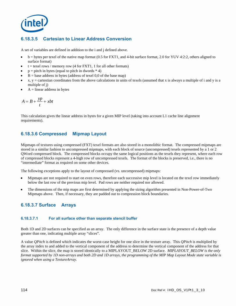
114 Doc Ref #: IHD_OS_V1Pt1_3_10
6.18.3.5 Cartesian to Linear Address Conversion
A set of variables are defined in addition to the i and j defined above.
• b = bytes per texel of the native map format (0.5 for FXT1, and 4-bit surface format, 2.0 for YUV 4:2:2, others aligned to surface format)
• t = texel rows / memory row (4 for FXT1, 1 for all other formats) • p = pitch in bytes (equal to pitch in dwords * 4) • B = base address in bytes (address of texel 0,0 of the base map) • x, y = cartestian coordinates from the above calculations in units of texels (assumed that x is always a multiple of i and y is a
multiple of j) • A = linear address in bytes
xbttypBA ++=
This calculation gives the linear address in bytes for a given MIP level (taking into account L1 cache line alignment requirements).
6.18.3.6 Compressed Mipmap Layout
Mipmaps of textures using compressed (FXT) texel formats are also stored in a monolithic format. The compressed mipmaps are stored in a similar fashion to uncompressed mipmaps, with each block of source (uncompressed) texels represented by a 1 or 2 QWord compressed block. The compressed blocks occupy the same logical positions as the texels they represent, where each row of compressed blocks represent a 4-high row of uncompressed texels. The format of the blocks is preserved, i.e., there is no “intermediate” format as required on some other devices.
The following exceptions apply to the layout of compressed (vs. uncompressed) mipmaps:
• Mipmaps are not required to start on even rows, therefore each successive mip level is located on the texel row immediately below the last row of the previous mip level. Pad rows are neither required nor allowed.
• The dimensions of the mip maps are first determined by applying the sizing algorithm presented in Non-Power-of-Two Mipmaps above. Then, if necessary, they are padded out to compression block boundaries.
6.18.3.7 Surface Arrays
6.18.3.7.1 For all surface other than separate stencil buffer
Both 1D and 2D surfaces can be specified as an array. The only difference in the surface state is the presence of a depth value greater than one, indicating multiple array “slices”.
A value QPitch is defined which indicates the worst-case height for one slice in the texture array. This QPitch is multiplied by the array index to and added to the vertical component of the address to determine the vertical component of the address for that slice. Within the slice, the map is stored identically to a MIPLAYOUT_BELOW 2D surface. MIPLAYOUT_BELOW is the only format supported by 1D non-arrays and both 2D and 1D arrays, the programming of the MIP Map Layout Mode state variable is ignored when using a TextureArray.
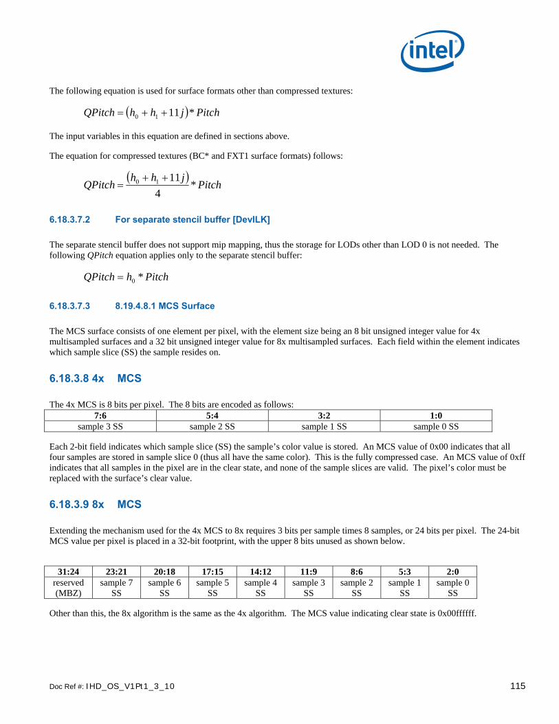
Doc Ref #: IHD_OS_V1Pt1_3_10 115
The following equation is used for surface formats other than compressed textures:
( ) PitchjhhQPitch *1110 ++=
The input variables in this equation are defined in sections above.
The equation for compressed textures (BC* and FXT1 surface formats) follows:
( )Pitch
jhhQPitch *
41110 ++
=
6.18.3.7.2 For separate stencil buffer [DevILK]
The separate stencil buffer does not support mip mapping, thus the storage for LODs other than LOD 0 is not needed. The following QPitch equation applies only to the separate stencil buffer:
PitchhQPitch *0=
6.18.3.7.3 8.19.4.8.1 MCS Surface
The MCS surface consists of one element per pixel, with the element size being an 8 bit unsigned integer value for 4x multisampled surfaces and a 32 bit unsigned integer value for 8x multisampled surfaces. Each field within the element indicates which sample slice (SS) the sample resides on.
6.18.3.8 4x MCS
The 4x MCS is 8 bits per pixel. The 8 bits are encoded as follows: 7:6 5:4 3:2 1:0
sample 3 SS sample 2 SS sample 1 SS sample 0 SS
Each 2-bit field indicates which sample slice (SS) the sample’s color value is stored. An MCS value of 0x00 indicates that all four samples are stored in sample slice 0 (thus all have the same color). This is the fully compressed case. An MCS value of 0xff indicates that all samples in the pixel are in the clear state, and none of the sample slices are valid. The pixel’s color must be replaced with the surface’s clear value.
6.18.3.9 8x MCS
Extending the mechanism used for the 4x MCS to 8x requires 3 bits per sample times 8 samples, or 24 bits per pixel. The 24-bit MCS value per pixel is placed in a 32-bit footprint, with the upper 8 bits unused as shown below.
31:24 23:21 20:18 17:15 14:12 11:9 8:6 5:3 2:0
reserved (MBZ)
sample 7 SS
sample 6 SS
sample 5 SS
sample 4 SS
sample 3 SS
sample 2 SS
sample 1 SS
sample 0 SS
Other than this, the 8x algorithm is the same as the 4x algorithm. The MCS value indicating clear state is 0x00ffffff.

116 Doc Ref #: IHD_OS_V1Pt1_3_10
6.18.3.9.1 MSS Surface
The physical MSS surface is stored identically to a 2D array surface, with the height and width matching the pixel dimensions of the logical multisampled surface. The number of array slices in the physical surface is 4 or 8 times that of the logical surface (depending on the number of multisamples). Sample slices belonging to the same logical surface array slice are stored in adjacent physical slices. The sampling engine ld2dss message gives direct access to a specific sample slice.
6.18.4 Cube Surfaces
The 3D pipeline supports cubic environment maps, conceptually arranged as a cube surrounding the origin of a 3D coordinate system aligned to the cube faces. These maps can be used to supply texel (color/alpha) data of the environment in any direction from the enclosed origin, where the direction is supplied as a 3D “vector” texture coordinate. These cube maps can also be mipmapped.
Each texture map level is represented as a group of six, square cube face texture surfaces. The faces are identified by their relationship to the 3D texture coordinate system. The subsections below describe the cube maps as described at the API as well as the memory layout dictated by the hardware.
6.18.4.1 Hardware Cube Map Layout
6.18.4.1.1 [Pre-Dev ILK]
The cube face textures are stored in the same way as 3D surfaces are stored (see section 0 for details). For cube surfaces, however, the depth is equal to the number of faces (always 6) and is not reduced for each MIP. The equation for DL is replaced with the following for cube surfaces:
6=LD
The “q” coordinate is replaced with the face identifier as follows:
“q”
coordinate face
0 +x 1 -x 2 +y 3 -y 4 +z 5 -z

Doc Ref #: IHD_OS_V1Pt1_3_10 117
6.18.4.1.2 [Dev ILK+]
The cube face textures are stored in the same way as 2D array surfaces are stored (see section 6.18.3 for details). For cube surfaces, the depth (array instances) is equal to 6. The array index “q” corresponds to the face according to the following table:
“q”
coordinate face
0 +x 1 -x 2 +y 3 -y 4 +z 5 -z
6.18.4.2 Restrictions
• The cube map memory layout is the same whether or not the cube map is mip-mapped, and whether or not all six faces are “enabled”, though the memory backing disabled faces or non-supplied levels can be used by software for other purposes.
• The cube map faces all share the same Surface Format

118 Doc Ref #: IHD_OS_V1Pt1_3_10
6.18.5 3D Surfaces
Multiple texture map surfaces (and their respective mipmap chains) can be arranged into a structure known as a Texture3D (volume) texture. A volume texture map consists of many planes of 2D texture maps. See Sampler for a description of how volume textures are used.
Figure 6-5. Volume Texture Map
B6688-01
q
u
v
Plane=0
Plane=0P=0
Mip 0 Mip 1 Mip 2
Note that the number of planes defined at each successive mip level is halved. Volumetric texture maps are stored as follows. All of the LOD=0 q-planes are stacked vertically, then below that, the LOD=1 q-planes are stacked two-wide, then the LOD=2 q-planes are stacked four-wide below that, and so on.
The width, height, and depth of LOD “L” are as follows:
( )( )( )( )1:?0
1:?0LheightLheightH
LwidthLwidthW
L
L
>>>>>=>>>>>=
This is the same as for a regular texture. For volume textures we add:
( )( )1:?0 LdepthLdepthDL >>>>>=
Cache-line aligned width and height are as follows, with i and j being a function of the map format as shown in Table 6-24.
⎟⎟⎠
⎞⎜⎜⎝
⎛=
⎟⎠⎞
⎜⎝⎛=
jHceiljh
iWceiliw
LL
LL
*
*
Note that it is not necessary to cache-line align in the “depth” dimension (i.e. lower case “d”).
The following equations for LODL,q give the base address Cartesian coordinates for the map at LOD L and depth q.

Doc Ref #: IHD_OS_V1Pt1_3_10 119
...
)*)3(*4
*2
*,*)8%((
)*)2(*2
*,*)4%((
)*)1(*,*)2%((
)*,0(
322
11
003,3
211
002,2
1001,1
0,0
hqhDceilhDceilhDwqLOD
hqhDceilhDwqLOD
hqhDwqLODhqLOD
q
q
q
q
>>+⎟⎠⎞
⎜⎝⎛+⎟
⎠⎞
⎜⎝⎛+=
>>+⎟⎠⎞
⎜⎝⎛+=
>>+=
=
These values are then used as “base addresses” and the 2D MIP Map equations are used to compute the location within each LOD/q map.
6.18.5.1 Minimum Pitch
The minimum pitch required to store the 3D map may in some cases be greater than the minimum pitch required by the LOD=0 map. This is due to cache line alignment requirements that may impact some of the MIP levels requiring additional spacing in the horizontal direction.
6.19 Surface Padding Requirements
6.19.1 Sampling Engine Surfaces
The sampling engine accesses texels outside of the surface if they are contained in the same cache line as texels that are within the surface. These texels will not participate in any calculation performed by the sampling engine and will not affect the result of any sampling engine operation, however if these texels lie outside of defined pages in the SNBT, a SNBT error will result when the cache line is accessed. In order to avoid these SNBT errors, “padding” at the bottom and right side of a sampling engine surface is sometimes necessary.
It is possible that a cache line will straddle a page boundary if the base address or pitch is not aligned. All pages included in the cache lines that are part of the surface must map to valid SNBT entries to avoid errors. To determine the necessary padding on the bottom and right side of the surface, refer to the table in Section 6.18.3.4 for the i and j parameters for the surface format in use. The surface must then be extended to the next multiple of the alignment unit size in each dimension, and all texels contained in this extended surface must have valid SNBT entries.
For example, suppose the surface size is 15 texels by 10 texels and the alignment parameters are i=4 and j=2. In this case, the extended surface would be 16 by 10. Note that these calculations are done in texels, and must be converted to bytes based on the surface format being used to determine whether additional pages need to be defined.
For buffers, which have no inherent “height,” padding requirements are different. A buffer must be padded to the next multiple of 256 array elements, with an additional 16 bytes added beyond that to account for the L1 cache line.
For cube surfaces, an additional two rows of padding are required at the bottom of the surface. This must be ensured regardless of whether the surface is stored tiled or linear. This is due to the potential rotation of cache line orientation from memory to cache.

120 Doc Ref #: IHD_OS_V1Pt1_3_10
For compressed textures (BC* and FXT1 surface formats), padding at the bottom of the surface is to an even compressed row, which is equal to a multiple of 8 uncompressed texel rows. Thus, for padding purposes, these surfaces behave as if j = 8 only for surface padding purposes. The value of 4 for j still applies for mip level alignment and QPitch calculation.
For YUV, 96 bpt, and 48 bpt surface formats, additional padding is required. These surfaces require an extra row plus 16 bytes of padding at the bottom in addition to the general padding requirements.
6.19.2 Render Target and Media Surfaces
The data port accesses data (pixels) outside of the surface if they are contained in the same cache request as pixels that are within the surface. These pixels will not be returned by the requesting message, however if these pixels lie outside of defined pages in the SNBT, a SNBT error will result when the cache request is processed. In order to avoid these SNBT errors, “padding” at the bottom of the surface is sometimes necessary.
If the surface contains an odd number of rows of data, a final row below the surface must be allocated. If the surface will be accessed in field mode (Vertical Stride = 1), enough additional rows below the surface must be allocated to make the extended surface height (including the padding) a multiple of 4.