wafer polish/grinder challenges
TRANSCRIPT
1July 16th, 2008
ACCRETECHACCRETECHEquipmentEquipment
Challenges for Challenges for 3D Interconnect3D Interconnect
Kazuo Kobayashi / Marketing Dept.

2
ACCRETECH CHALLENGE
• Handling System ( WSS / Tape )• Thinning ( Grinding WPH)• Thinning ( C M Polishing / Etching)• Cleaning ( particle / contamination)• Chemistry( Environment )• Low temperature process • Dicing (Diamond Blade >>> Z axis control)• Dicing (Ablation Laser for device cutting)• Dicing (Laser Scribing for precise energy control) • Stress relief. ( back-side + die-side )• DAF ( coating / printing / cutting )

3
2008: Set for further growth and increased production capacity:
+ 15,900m2 ground, +50% vs. today
Hachioji PlantBldg. for PG, Dicer & CMPCompleted in March 2005
ACCT Tower
Building #1 / #2
(Prober)
Building #4(Win-Win)
Parts Control
Building #3(Dicer, PG,
CMP)
New Land for
next Factory
Challenging Site
4
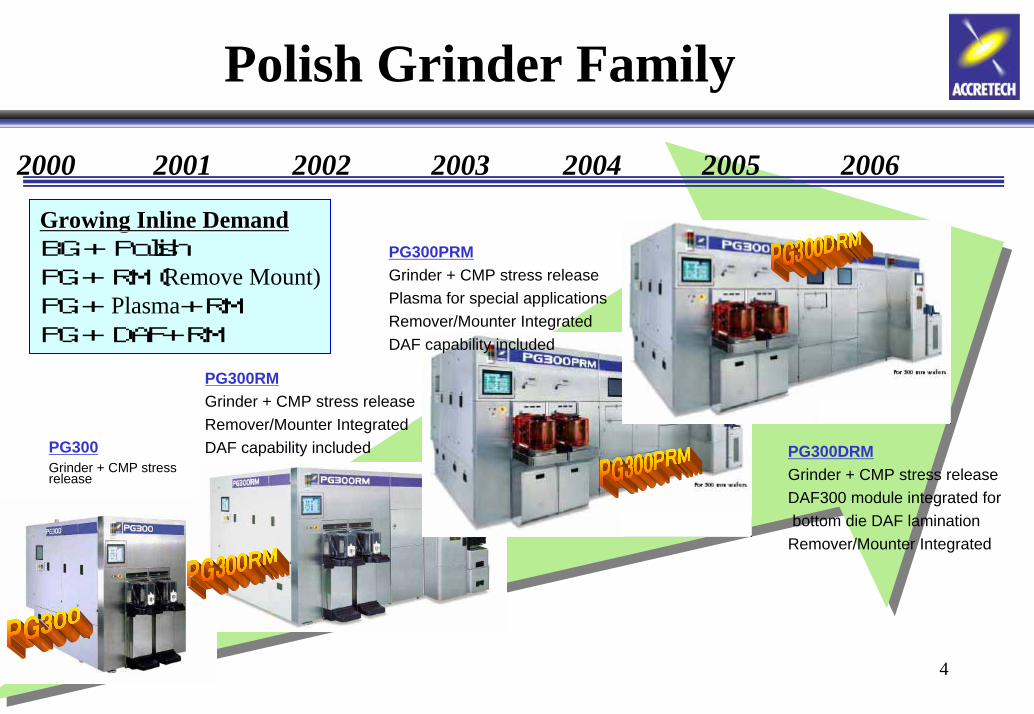
Polish Grinder Family
2000 2001 2002 2003 2004 2005 2006
PG300Grinder + CMP stress release
PG300RMGrinder + CMP stress releaseRemover/Mounter IntegratedDAF capability included
PG300PRMGrinder + CMP stress releasePlasma for special applicationsRemover/Mounter IntegratedDAF capability included
PG300DRMGrinder + CMP stress releaseDAF300 module integrated forbottom die DAF lamination
Remover/Mounter Integrated
Growing Inline DemandGrowing Inline DemandBG+ PolishPG+ RM(Remove Mount)PG+ Plasma+RMPG+DAF+RM

5
Blade Dicer family
A-WD-10B A-WD-100A A-WD-110A A-WD-250S
A-WD-200T
ML200
A-WD-300T
A-WD-300T
with Load Port
A-WD-300TXPS280

6
Laser Dicer familyML200
ML300RME
PG300+ML300+RM
DC tape expander
Laser scribing
300mm/sec
IR picture
MAHOH LASER
MAHO :magic in Japanese
7
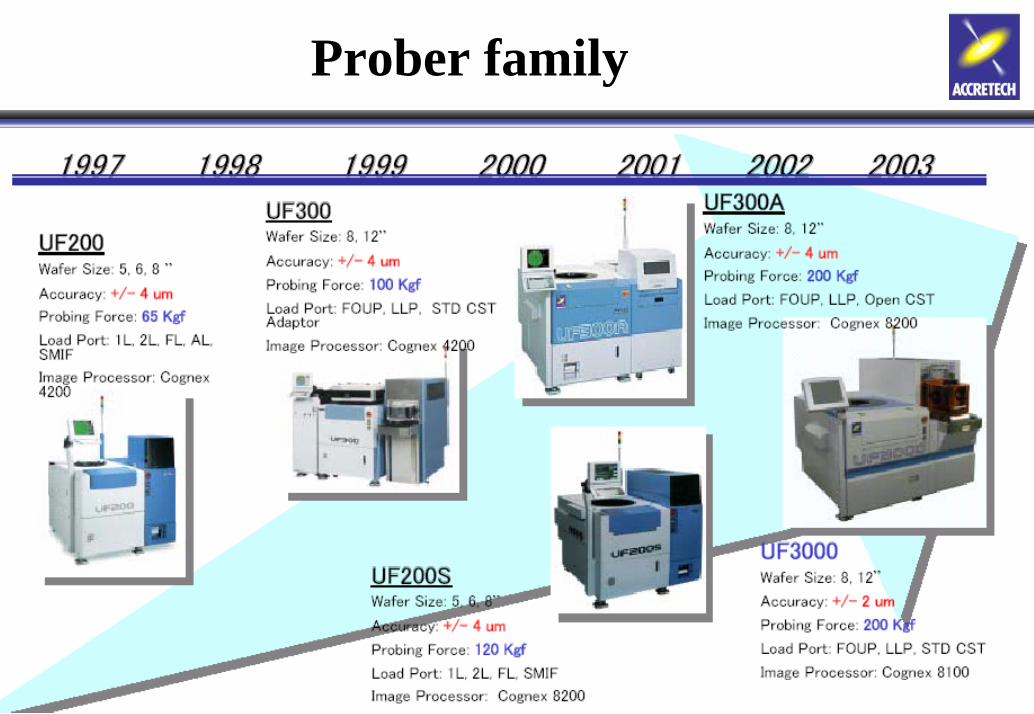
Prober family

8
Thin Wafers

9
Rolled up after Grinding
45um 50um 55um

10
Thin Wafers
TransparencyTransparency
5 micron thick wafer
Rolled by device and BG tape & pattern.

11
HANDLING
Hard wf. Support System
12 micron
⇒ COST⇒ Accuracy (TTV, Uniformity)⇒ Thermal Expansion Rate⇒ Chemical
6 micron
Frame Handling System
Challenge
more > less← →
⇒ Accuracy (TTV, Uniformity)⇒ Universal chuck ⇒ Chemical
Tape Adhesive glass wafer
Si

12
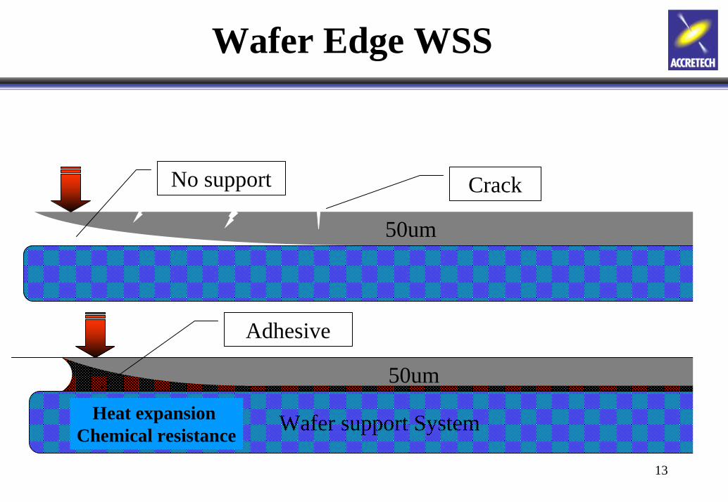
Wafer Edge
360um
180um
50um25um
WET Etched wafer
13
Wafer Edge WSS
50um
Wafer support System
50um
Adhesive
No support Crack
Heat expansion Chemical resistance
14
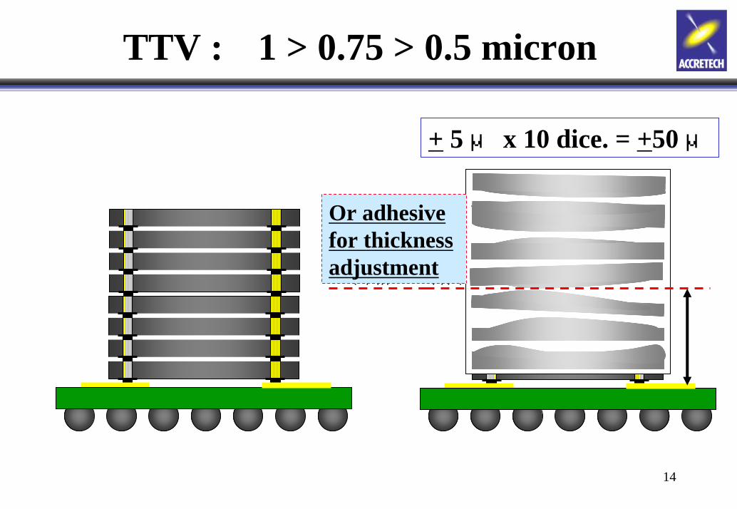
TTV : 1 > 0.75 > 0.5 micron
基準面からの平坦化に接着剤や平面加工を採用
+ 5 μ x 10 dice. = +50 μ
Or adhesive for thickness adjustment
15
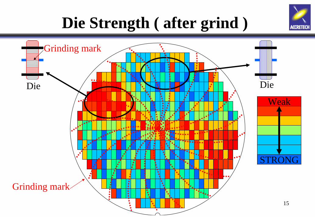
Die Strength ( after grind )
Weak
STRONG
Grinding mark
Die Die
Grinding mark
16
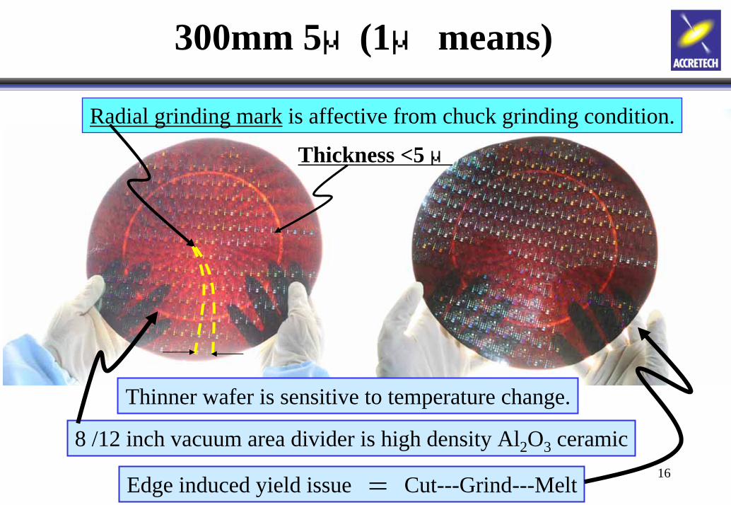
300mm 5μ(1μ means)
Edge induced yield issue = Cut---Grind---Melt
Thickness <5 μ
Radial grinding mark is affective from chuck grinding condition.
Thinner wafer is sensitive to temperature change.
8 /12 inch vacuum area divider is high density Al2O3 ceramic

17
HANDLING
Universal Size Chuck on Grinding
6 micron
Vacuum Chuck Transfer
Thermal Expansion rate
12 micron

18
Non-Contact Gauge
Air Inlet
Air Nozzle
• Post Process
• Pre-Process
• In-Process
• Response
• Accuracy
• Maintenance
Wet WaferIR Laser
Air Blow
Laser

19
DC frame chuck for thinning
10μ20μ
Vacuum Clamping Chuck
WaferBG tape
Frame
Cup type Grinding wheel
20
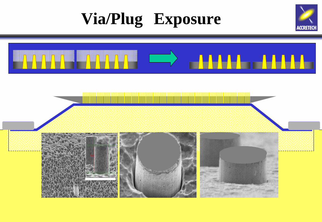
Via/Plug Exposure
21
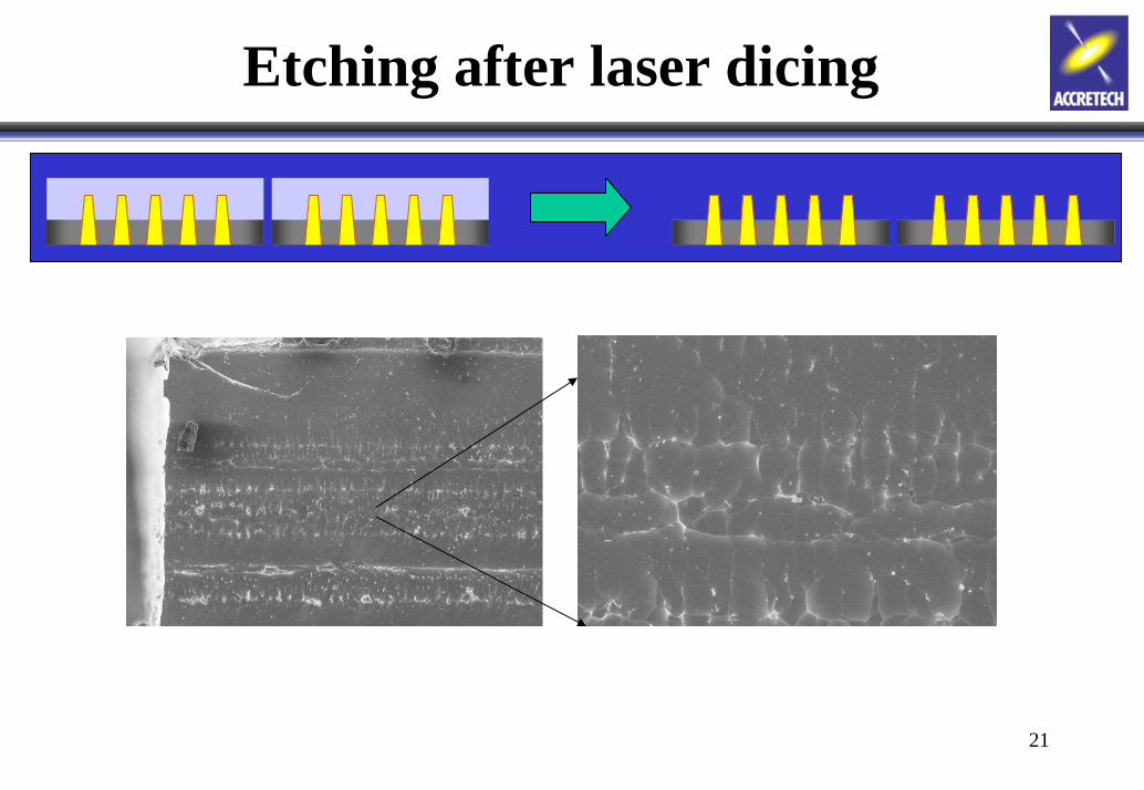
Etching after laser dicing
22
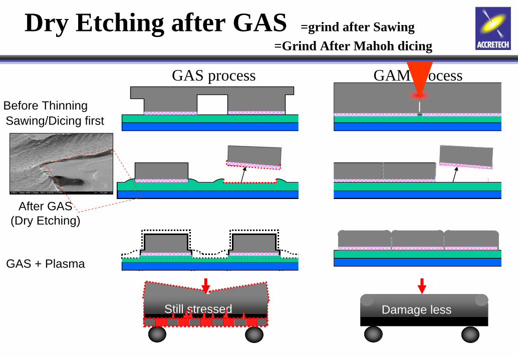
Dry Etching after GAS =grind after Sawing=Grind After Mahoh dicing
Before Thinning
After GAS(Dry Etching)
GAS + Plasma
Sawing/Dicing first
Still stressed
GAS process GAM process
Damage less

23
DAF cutting (after GAS vs GAM)
Die moves after “Grind After Sawing” or “Dice Before Grinding”DAF must be cut by laser after measuring the die to die center position.This takes time and street width expands 3 times.
DieDie
DieDie
Die
Die
DieLaser
24
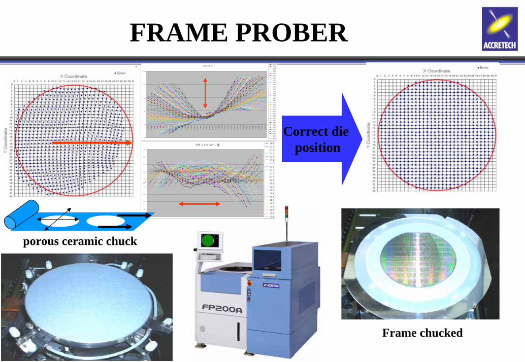
FRAME PROBER
porous ceramic chuck
Frame chucked
Correct die position
X列ごとのXズレ
-50
0
50
100
150
200
Y=109
Y=110
Y=111
Y=112
Y=113
Y=114
Y=115
Y=116
Y=117
Y=118
Y=119
Y=120
Y=121
Y=122
Y=123
Y=124
Y=125
Y=126
Y=127
Y=128
Y=129
Y=130
Y=131
Y=132
Y=133
Y=134
Y=135
Y=136
Y=137
Y=138
Y=139
Y=140
Y=141
Y=142
Y=143
Y=144
Y=145
Y=146
Y=147
106
107
108
109
110
111
112
113
114
115
116
117
118
119
120
121
122
123
124
125
126
127
128
129
130
131
132
133
134
135
136
137
138
139
Y列 ごとの Yズ レ量
-50
- 4 0
- 3 0
- 2 0
- 1 0
0
1 0
2 0
3 0
4 0
X=106
X=108
X=110
X=112
X=114
X=116
X=118
X=120
X=122
X=124
X=126
X=128
X=130
X=132
X=134
X=136
X=138
X=140
X=142
X=144
X=146
X=148
1 09
110
111
112
113
114
115
116
117
118
119
120
121
122
123
124
125
126
127
128
129
130
131

25
DAF coating systemDAF coating system
Y-Axis
X-Axis
θAxisA-Loader
B-Loader
Plasma Electrode
Coating Stage
Baking Stage
Inspection StageH4 Handler
PG Side RM Side
H4 Handler
Z-Axis
Masking the dicing street on coatingor inc-jet print for thinner DAF.
Screen printing

26
“GAM system ”
MAHO + PG300RM + Expansion + (DB)*-**
4 3
1 2
0 25
*-**
UV
RM300E
PG300
ML300
Convertible to Blade dicing
Flexible for Die Bonders
Connectable to Frame prober,
Die bonder
connectable for Plasma.

27
PG+Mahoh (GAM) Integration System
Integration system for thin wafer
Mahoh Laser
Transfer Arm
Transfer Arm
28
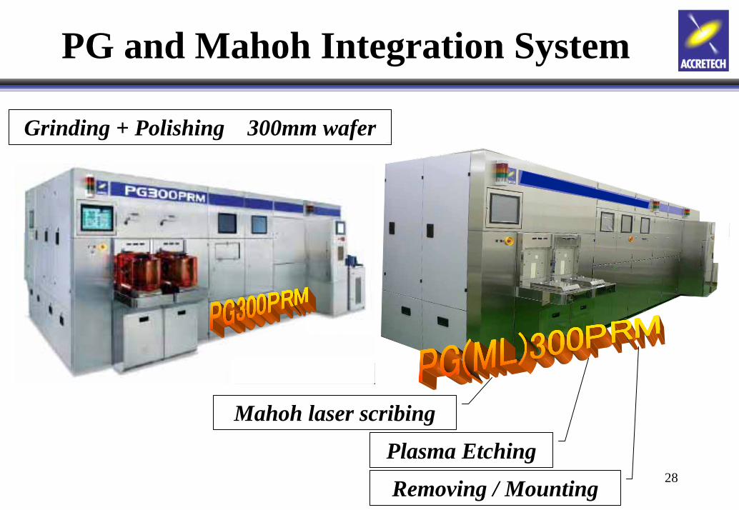
PG and Mahoh Integration System
Mahoh laser scribing
Plasma Etching
Grinding + Polishing 300mm wafer
Removing / Mounting

29
Thin Die
Accretech : North Hall 5571.

30
Wafer Thinning SystemWafer Thinning SystemTurn Key Solution = Handling & Cleaning
UV Curing UnitCoin Stack OptionOff-line Cassette Option
Post Process Gauge
Protection TapeLaminating
WaferThinning
StressRelief
Die Attach FilmLaminating
Dicing Tape Mounting
Protection Tape Peeling
Dicing Die Bonding
Film Frame Probing
Laser Dicer Integration
ACC300
Dicing Tape Expanding
For Stacked Dicing Tape with DAF Layer
Angle CutLamination for Bump Wafer
Wet PolishingDry PolishingWet EtchingDry Etching
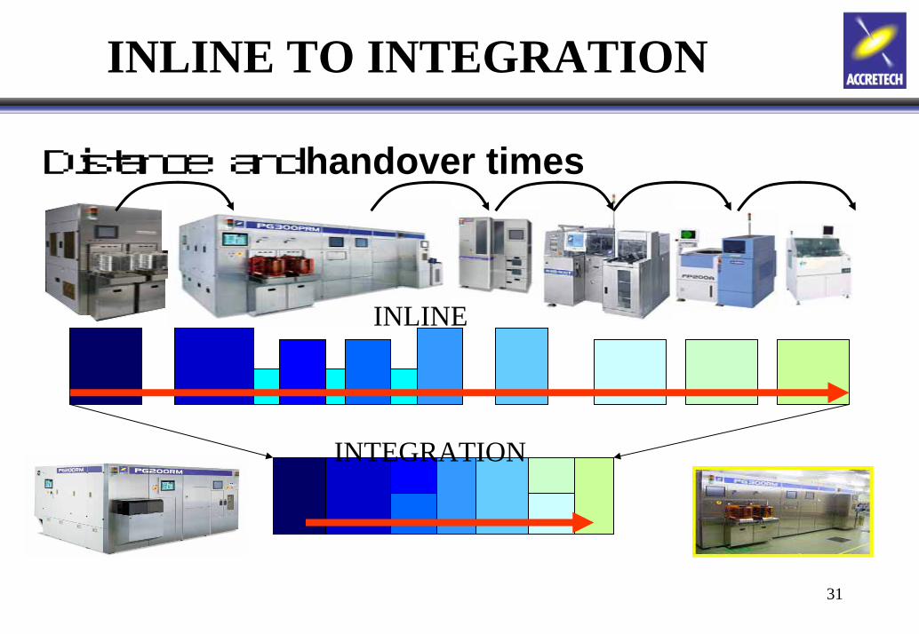
31
INLINE TO INTEGRATION
INLINE
INTEGRATION
Distance and handover times
32
Challenge for future Integration
*-**
4 3
1 2
0 25
*-**
0 25
*-**
4 3
1 2
0 25
*-**
0 25
PG300/BG300
UV
RM300
EXPANDER
ACC300
UV
ML300 Laser
Plasma
Etcher
WBC=DAF
BG+Polish
United multi laser source
Edge grinding
ScribingTrigger
&Gettering Device grooving
Laser + Blade
Pressure controlFor bumped wafers
CleaningCleaning
Plasma etching
Sivia
DAF cuttinglaser
BG tape Frame handlingChuck table handling

33
Thank you !MOSCONE CENTER
North Hall 5571. Come and Feelthe die strength!