winter 14 examination - pcpolytechnic
TRANSCRIPT

MAHARASHTRA STATE BOARD OF TECHNICAL EDUCATION (Autonomous)
(ISO/IEC - 27001 - 2005 Certified)
___________________________________________________________________________________________
1
WINTER– 14 EXAMINATION
Subject Code: 17319 Model Answer
Important Instructions to examiners:
1) The answers should be examined by key words and not as word-to-word as given in the model
answer scheme.
2) The model answer and the answer written by candidate may vary but the examiner may try to
assess the understanding level of the candidate.
3) The language errors such as grammatical, spelling errors should not be given more Importance
(Not applicable for subject English and Communication Skills.
4) While assessing figures, examiner may give credit for principal components indicated in the
figure. The figures drawn by candidate and model answer may vary. The examiner may give credit
for any equivalent figure drawn.
5) Credits may be given step wise for numerical problems. In some cases, the assumed constant
values may vary and there may be some difference in the candidate’s answers and model answer.
6) In case of some questions credit may be given by judgement on part of examiner of relevant
answer based on candidate’s understanding.
7) For programming language papers, credit may be given to any other program based on
equivalent concept.

MAHARASHTRA STATE BOARD OF TECHNICAL EDUCATION (Autonomous)
(ISO/IEC - 27001 - 2005 Certified)
___________________________________________________________________________________________
2
1. a) Attempt Any Six of the following: (12 Marks)
i) List various transistor biasing methods.
Ans. (Any 4 methods – 2 Marks)
Various biasing methods of transistor are:
Fixed Bias
Base Bias
Base Bias with Collector feedback
Voltage Divider
Base Bias with Emitter Feedback
ii) Define α of Transistor.
Ans. (Correct definition – 2 Marks)
Current Gain of Transistor (α):
It is defined as the ratio of collector current (IC) to the emitter current (IE).
Mathematically it is expressed as, α =
.
iii) State the need of cascade amplifier.
Ans. (Any relevant correct explanation – 2 Marks to be given.)
Need of Cascade Amplifier:
The output from a single stage amplifier is usually insufficient to drive an output device. So that additional amplification over two or three stages is necessary.
To achieve this, output of each amplifier stage is coupled in some way to the input of the next
stage.
The resulting system is referred to as multi-stage amplifier or cascade amplifier, where the
output of first amplifier is fed as input to second amplifier.
iv) Define intrinsic standoff ratio for UJT.
Ans. (Correct definition – 2 Marks)
The ratio of
is called as Intrinsic Standoff Ratio of UJT (η).
Where, RB1 = resistance between B1 terminal and emitter terminal.
RB2 = resistance between B2 terminal and emitter terminal.
RBB = RB1+ RB2
v) Define operating principle of tuned circuit.
Ans. (Correct definition – 1 Mark, Any relevant diagram – 1 Mark)
The working of tuned voltage amplifier may be understood by considering a radio frequency signal,
to be amplified applied at the input of the amplifier. The resonant frequency of the tuned circuit is made equal to the frequency of the input signal by changing the value of capacitor (C) and inductor (L).when the frequency of the tuned circuit becomes equal to that of the input signal a large signal
appears across the output terminals.
If the input signal is a complex wave (i.e. it contains many frequency components.) in that case the
frequency with input frequency equal to the resonant frequency will be amplified. And all the other frequencies will be rejected by the tuned circuit.

MAHARASHTRA STATE BOARD OF TECHNICAL EDUCATION (Autonomous)
(ISO/IEC - 27001 - 2005 Certified)
___________________________________________________________________________________________
3
vi) List the types of Power Amplifiers.
Ans. (Any 4 Correct Power Amplifiers– 2 Marks)
1. Class A Power Amplifier
2. Class B Power Amplifier
3. Class AB Power Amplifier
4. Class C Power Amplifier
5. Class D Power Amplifier
vii) State the effect of VGS on channel conductivity of N – Channel JFET.
Ans. (Correct explanation – 1 Mark, Any relevant correct diagram – 1 Mark)
When a reverse voltage VGS is applied between the Gate and Source terminal, the width of the
depletion layers is increased.
This reduces the width of conducting channel thereby increasing the resistance of n – type bar
consequently; the current from source to drain is decreased.
MAHARASHTRA STATE BOARD OF TECHNICAL EDUCATION (Autonomous)
(ISO/IEC - 27001 - 2005 Certified)
___________________________________________________________________________________________
4
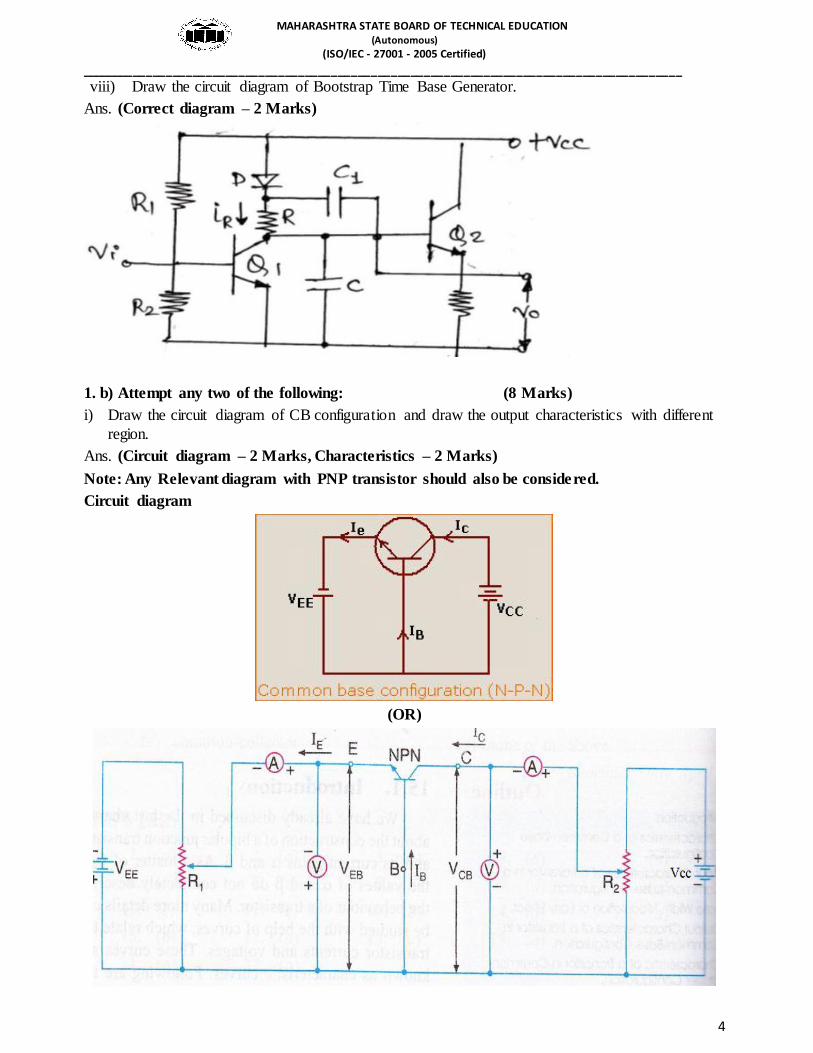
viii) Draw the circuit diagram of Bootstrap Time Base Generator.
Ans. (Correct diagram – 2 Marks)
1. b) Attempt any two of the following: (8 Marks)
i) Draw the circuit diagram of CB configuration and draw the output characteristics with different
region.
Ans. (Circuit diagram – 2 Marks, Characteristics – 2 Marks)
Note: Any Relevant diagram with PNP transistor should also be considered.
Circuit diagram
(OR)

MAHARASHTRA STATE BOARD OF TECHNICAL EDUCATION (Autonomous)
(ISO/IEC - 27001 - 2005 Certified)
___________________________________________________________________________________________
5
Output Characteristics
ii) Draw the circuit diagram of fixed voltage bias method and describe its working.
Ans. (Diagram 2 Marks, Working – 2 Marks)
In this circuit the gate supply voltage (-VGG) is used to ensure that the gate source junction is reverse biased. Since there is no gate current, there is no voltage drop across RG.
The fixed bias cannot provide a stable Q- point from JFET to another.
Resistor RG is used for ac operation purpose. Thus, resistor RG has a little to do with the dc operation of the amplifier.
Apply KVL to gate circuit,
VGG + VGS = 0
Therefore, VGS = - VGG
As VGG is a constant voltage, the name of this configuration is fixed bias configuration.
The drain current is given by,
ID = IDSS *
+2
The drain to source voltage can be obtained by applying KVL to the drain circuit,
VDD – IDRD – VDS = 0
Therefore, VDS = VDD – IDRD.
MAHARASHTRA STATE BOARD OF TECHNICAL EDUCATION (Autonomous)
(ISO/IEC - 27001 - 2005 Certified)
___________________________________________________________________________________________
6
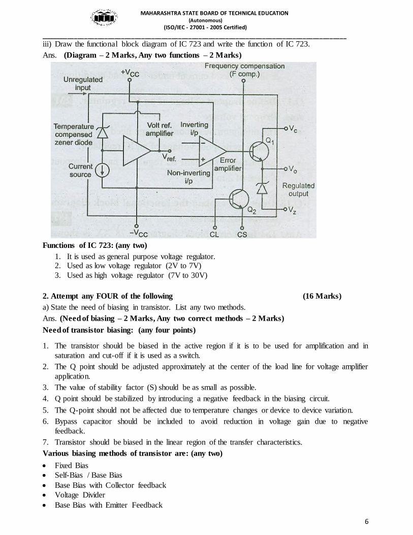
iii) Draw the functional block diagram of IC 723 and write the function of IC 723.
Ans. (Diagram – 2 Marks, Any two functions – 2 Marks)
Functions of IC 723: (any two)
1. It is used as general purpose voltage regulator. 2. Used as low voltage regulator (2V to 7V)
3. Used as high voltage regulator (7V to 30V)
2. Attempt any FOUR of the following (16 Marks)
a) State the need of biasing in transistor. List any two methods.
Ans. (Need of biasing – 2 Marks, Any two correct methods – 2 Marks)
Need of transistor biasing: (any four points)
1. The transistor should be biased in the active region if it is to be used for amplification and in
saturation and cut-off if it is used as a switch.
2. The Q point should be adjusted approximately at the center of the load line for voltage amplifier
application.
3. The value of stability factor (S) should be as small as possible.
4. Q point should be stabilized by introducing a negative feedback in the biasing circuit.
5. The Q-point should not be affected due to temperature changes or device to device variation.
6. Bypass capacitor should be included to avoid reduction in voltage gain due to negative
feedback.
7. Transistor should be biased in the linear region of the transfer characteristics.
Various biasing methods of transistor are: (any two)
Fixed Bias
Self-Bias / Base Bias
Base Bias with Collector feedback
Voltage Divider
Base Bias with Emitter Feedback

MAHARASHTRA STATE BOARD OF TECHNICAL EDUCATION (Autonomous)
(ISO/IEC - 27001 - 2005 Certified)
___________________________________________________________________________________________
7
b) Draw the circuit diagram of voltage divider bias method and describe it’s working.
Ans. (Circuit Diagram – 2 Marks, Any relevant Working – 2 Marks)
Fig. below shows the voltage divider.
In this method two resistances R1 and R2 are connected across the supply voltage VCC and
provide biasing.
The voltage drop across resistor R2 forward biases the base emitter junction of transistor. The
resistor RE provides the d.c. stability.

MAHARASHTRA STATE BOARD OF TECHNICAL EDUCATION (Autonomous)
(ISO/IEC - 27001 - 2005 Certified)
___________________________________________________________________________________________
8
c) Draw the construction of N-channel JFET and explain its working.
Ans.
Construction (1 Mark)
Working (Diagram – 1 Mark, Explanation – 2 Marks)
1. VGS = 0V
When a voltage is applied between the drain & source with a D.C supply voltage (VDD) with VGS = 0V, the electrons flows from source to drain through the narrow channel existing between the
depletion regions. This constitutes drain current (ID). The value of drain current is maximum when VGS = 0V. This current is designated by the symbol IDSS.
2. When VGS is negative
When VGS is increased above zero, the reverse voltage across the gate source junction is increased. As a result depletion regions are widened. This reduces effective width of channel therefore
controls the flow of drain current through the channel.
If VGS increased further, two depletion regions touch each other. The drain current reduces to 0.The gate to source at which drain current reduces to 0 is called as pinch off voltage

MAHARASHTRA STATE BOARD OF TECHNICAL EDUCATION (Autonomous)
(ISO/IEC - 27001 - 2005 Certified)
___________________________________________________________________________________________
9
d) What is Amplifier? Give its classification.
Ans. (Amplifier definition – 1 Mark, Any three classifications – 3 Marks)
Amplifier: The circuit which amplifies input signal is called as an amplifier.
Classification of amplifier is based on various factors as given below:
1. Classification based on purpose of amplification
Voltage amplifier
Power amplifier
2. Classification based on frequency range
AF amplifier: (20 Hz to 20 KHz)
RF amplifier: (typically more than 100 KHz)
3. Classification based on the position of Q point
Class A amplifier
Class B amplifier
Class C amplifier
Class AB amplifier
4. Classification depending on the type of coupling
Direct Coupled amplifier
RC coupled amplifier
Transformer coupled amplifier
e) State the effect of negative feedback on voltage gain, bandwidth, input impedance, output impedance.
Ans. (Four correct points – 1 Mark each)
Sr.No Parameters Negative Feedback
1 Voltage Gain Decreases
2 Bandwidth Increases
3 Input Impedance Increases
4 Output Impedance Decreases
f) Draw the block diagram of regulated power supply. State the function of each block.
Ans. (Block Diagram – 2 Marks, Explanation – 2 Marks)
(OR)

MAHARASHTRA STATE BOARD OF TECHNICAL EDUCATION (Autonomous)
(ISO/IEC - 27001 - 2005 Certified)
___________________________________________________________________________________________
10
There are four basic blocks of a D.C. regulated power supply. They are 1) Step down transformer 2) Rectifier 3) Filter 4) Voltage Regulator.
Functions of each block are as follows:
Step down transformer: Reduces 230 volts 50Hz ac voltage to required ac voltage level.
Rectifier: Rectifier converts ac voltage to dc voltage. Typically bridge full wave rectifier is widely
used.
Filter: Filter is a circuit used to remove fluctuations (ripple or ac) present in dc output.
Voltage Regulator: Voltage regulator is a circuit which provides constant dc output voltage irrespective of changes in load current or changes in input voltage. Voltage divider is a passive circuit used for providing different dc voltages required by different electronic circuits.
3. Attempt any FOUR of the following (16 Marks)
a) Compare CB, CE, and CC of BJT with reference to the following points
1. Input Impedance 2. Current Gain
3. Output Impedance 4. Voltage Gain
Ans. (4 Correct Points – 1 Mark each)
Sr. No Parameter CB CE CC
1 Input impedance Low
(OR)
50Ω
Medium
(OR)
600Ω to 4KΩ
High
(OR)
1MΩ
2 Current gain less than or equal to 1
(OR)
α =
High
(OR)
β =
Very high
(OR)
γ =
3 Output
impedance High
(OR)
50KΩ
Medium
(OR)
10KΩ to 50KΩ
Low
(OR)
50Ω
4 Voltage gain High
(OR)
High
(OR)
Less than or equal to 1
(OR)

MAHARASHTRA STATE BOARD OF TECHNICAL EDUCATION
(Autonomous) (ISO/IEC - 27001 - 2005 Certified)
_____________________________________________________________________________________________
11
b) Explain how JFET acts as a voltage controlled device.
Ans. (Diagram – 2 Marks, Correct explanation – 2 Marks)
The gain of the common emitter amplifier Q1 is controlled.
The output signal vo is rectified and filtered and the dc voltage proportional to vo is applied to the gate of FET operating in the Ohmic region.
Depending on the dc gate voltage, the resistance rDS of FET will change; this will change the emitter resistance of Q1 since RE is in parallel with rDS.
The gain of a CE amplifier is approximately equal to – RC/ RE. Hence change in RE will change the gain automatically.
If vo increases, then dc voltage at the rectifier filter output will increase. Hence VGS becomes more negative. This decreases ID or increases rDS of FET. Hence the parallel combination
(RE rDS) will increase and the gain of Q1 if vo decreases. This is how the automatic gain control is achieved.
c) State the Barkhausen Criterion for the generation of sustained oscillations and draw the block
diagram of an oscillator.
Ans. (Barkhausen Criterion – 2 Marks, Block Diagram – 2 Marks)
Barkhausen criteria:
a) Total phase shift should be 360° or 0°
b) Loop gain greater than and equal to unity i.e. | |>= 1
(OR)

MAHARASHTRA STATE BOARD OF TECHNICAL EDUCATION
(Autonomous) (ISO/IEC - 27001 - 2005 Certified)
_____________________________________________________________________________________________
12
d) Draw the frequency response of direct coupled amplifier. Discuss its advantages and
disadvantages.
Ans. (Frequency Response – 2 Marks, Advantages & Disadvantages – 2 Marks)
Two stage Direct Coupled Amplifier Frequency Response
Advantages: (any 2) 1) Wide frequency response (large Bandwidth)
2) Reduced cost and complexity due to absence of coupling capacitors. 3) This amplifier can amplify even the dc signals.
Disadvantages: (any 2)
1) The output waveform has a dc shift.
2) Poor frequency response at higher frequencies. 3) Poor temperature stability.
e) State the working principle of 79XX series voltage regulator with diagram.
Ans. (diagram – 2 Marks, explanation – 2 Marks)
The capacitor C1 (typically 0.22μF) is required only if the power supply filter is located more than 3
inches away from the IC regulator. The capacitor C2 (typically 1μF) is required for stability of the
output voltage.
Both the capacitors must be solid tantalum capacitors.

MAHARASHTRA STATE BOARD OF TECHNICAL EDUCATION
(Autonomous) (ISO/IEC - 27001 - 2005 Certified)
_____________________________________________________________________________________________
13
Figure above shows the 79XX to produce an adjustable output voltage. The capacitor C3 (typically
25μF) improves the transient response of output voltage. The output voltage is given by the
equation,
Vout = Vfixed =(
)
f) Draw the circuit diagram of series transistor voltage regulator and describe its operation.
Ans. (Correct circuit diagram – 2 Marks, Operation – 2 Marks)
Above fig. shows a circuit of a transistor series regulator. Since the transistor is connected in series with the load, therefore the circuit is known as a series regulator.
Operation:-
The unregulated DC supply is fed to the input terminal as shown in above fig.
The output voltage is given by VL= VZ – VBE
VZ being a zener voltage is assumed to be a constant therefore if the output voltage varies, and
then there will be a change in VBE.
If the output voltage increases due to some region then VBE decreases and due to this base
current decreases. Therefore collector current decreases.
This will increase the collector to emitter voltage (VCE) across the transistor and VL will be
regulated. this is because VL = Vs – VCE.
If the output voltage decreases then exactly opposite action will takes place and the output
voltage is regulated.
The circuit action may be summarized in the form of the following equation.
VL↑ → VBE↓ →IB↓→IC↓ → VCE↑→ VL ↓

MAHARASHTRA STATE BOARD OF TECHNICAL EDUCATION
(Autonomous) (ISO/IEC - 27001 - 2005 Certified)
_____________________________________________________________________________________________
14
4. Attempt any FOUR of the following (16 Marks)
a) Draw the symbol and construction of N – channel JFET.
Ans. (Symbol – 2 Marks, Construction – 2 Marks)
(OR)
Symbol
Construction
b) Draw the circuit of double tuned amplifier and sketch the frequency response.
Ans. (Circuit diagram – 2 Marks, Frequency response – 2 Marks)

MAHARASHTRA STATE BOARD OF TECHNICAL EDUCATION
(Autonomous) (ISO/IEC - 27001 - 2005 Certified)
_____________________________________________________________________________________________
15
Frequency Response
c) Compare BJT and JFET with reference to the following points
1. Symbol
2. Transfer Characteristics
3. Input Impedance
4. Application
Ans. (each correct point – 1 Mark)
Parameters BJT JFET
Symbol
Transfer
Characteristics
Linear Non- Linear
Impedance Low input impedance
(in KΩ)
Input impedance is high
(in MΩ)
Applications
(any two)
Amplifiers, Oscillators,
Digital Circuits, etc.
Amplifiers, Oscillators,
Digital Circuits, etc.
MAHARASHTRA STATE BOARD OF TECHNICAL EDUCATION
(Autonomous) (ISO/IEC - 27001 - 2005 Certified)
_____________________________________________________________________________________________
16
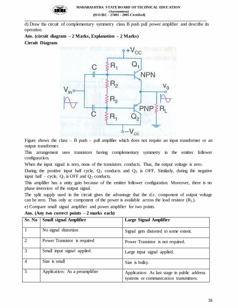
d) Draw the circuit of complementary symmetry class B push pull power amplifier and describe its
operation.
Ans. (circuit diagram – 2 Marks, Explanation – 2 Marks)
Circuit Diagram
Figure shows the class – B push – pull amplifier which does not require an input transformer or an
output transformer.
This arrangement uses transistors having complementary symmetry in the emitter follower
configuration.
When the input signal is zero, none of the transistors conducts. Thus, the output voltage is zero.
During the positive input half cycle, Q1 conducts and Q2 is OFF. Similarly, during the negative
input half – cycle, Q1 is OFF and Q2 conducts.
This amplifier has a unity gain because of the emitter follower configuration. Moreover, there is no
phase inversion of the output signal.
The split supply used in the circuit gives the advantage that the d.c. component of output voltage can be zero. Thus only ac component of the power is available across the load resistor (RL).
e) Compare small signal amplifier and power amplifier for two points.
Ans. (Any two correct points – 2 marks each)
Sr. No Small signal Amplifier Large Signal Amplifier
1 No signal distortion Signal gets distorted to some extent.
2 Power Transistor is required Power Transistor is not required.
3 Small input signal applied. Large input signal applied.
4 Size is small Size is bulky.
5 Application: As a preamplifier Application: As last stage in public address
systems or communication transmitters.

MAHARASHTRA STATE BOARD OF TECHNICAL EDUCATION
(Autonomous) (ISO/IEC - 27001 - 2005 Certified)
_____________________________________________________________________________________________
17
f) Draw the V- I Characteristics of UJT and label it.
Ans. (Correct characteristics with labeling – 4 Marks)
(OR)
5. Attempt any FOUR of the following (16 Marks)
a) In CE configuration if β = 99 and leakage current ICEO = 50μA, if base current is 0.5 mA, Determine IC and IE.
Ans. (IC – 2 Marks and IE – 2 Marks)
Given: β= 99, ICEO = 50 μA, IB = 0.5 mA, = 500 μA
To Find: IC & IE
Solution:
IC = β IB + ICEO
Therefore, IC = 99 x 500 + 50 = 49550μA
Therefore, IC = 49.55 mA
IE = IC + IB
= 49.55 mA + 0.5 mA = 50.05mA
IE = 50.05 mA
MAHARASHTRA STATE BOARD OF TECHNICAL EDUCATION
(Autonomous) (ISO/IEC - 27001 - 2005 Certified)
_____________________________________________________________________________________________
18
b) Compare RC oscillator and crystal oscillator with reference to following points
1. Frequency stability
2. Example (any relevant example should be considered) 3. Application (any relevant application should be considered) 4. Frequency Formula
Ans. (Each correct point – 1 Mark)
Sr. No Parameter RC oscillator Crystal Oscillator
1 Frequency Stability Poor Best
2 Example RC Phase Shift Oscillator Pierce Crystal Oscillator
3 Application Used for audio frequency range applications having range from
several Hz to 100KHz.
Used for radio frequency range applications like communication
transmitters having range Upto 10MHZ.
4 Frequency
Formula =
√ =
√
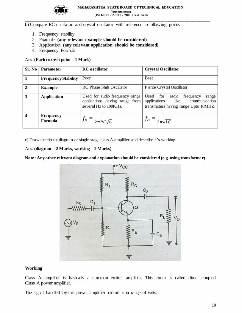
c) Draw the circuit diagram of single stage class A amplifier and describe it’s working.
Ans. (diagram – 2 Marks, working – 2 Marks)
Note: Any other relevant diagram and explanation should be considered (e.g. using transformer)
Working
Class A amplifier is basically a common emitter amplifier. This circuit is called direct coupled Class A power amplifier.
The signal handled by this power amplifier circuit is in range of volts.

MAHARASHTRA STATE BOARD OF TECHNICAL EDUCATION
(Autonomous) (ISO/IEC - 27001 - 2005 Certified)
_____________________________________________________________________________________________
19
The transistor used is power transistor, capable of operating in the range of few watts.
In the class A amplifier, the transistor bias and amplitude of input signal are such that the output
current flow for the complete cycle (i.e. 3600) of input signal.
This above condition is achieved by locating the Q – point somewhere near the centre of the load
line.
In order to obtain the maximum output signal the Q – point is set at the centre of the load line.
d) List four applications of FET’s.
Ans. (any four correct applications – 4 Marks)
Applications of FET
1. FET can be used as an amplifier.
2. FET can be used as a switch.
3. It can be used as analog switch in circuits like sample and hold, amplitude modulation,
ADC/DAC (analog to digital or digital to analog) converters.
4. As a voltage variable resistor (VVR)
5. In digital circuits.
e) Draw the circuit diagram of crystal oscillator and give the basic principle of piezoelectric crystal.
Ans. (Circuit of crystal oscillator – 2 Marks, Principle of crystal – 2 Marks)
Note: Circuit of crystal oscillator using FET or Op-Amp should be considered
Circuit Diagram of Crystal Oscillator
Working Principle of Piezoelectric Crystal
A Quartz Crystal has a very peculiar property known as Piezoelectric Effect.
According to this effect, when an AC voltage is applied across a quartz crystal, it vibrates at a
frequency of applied voltage.
Conversely, if a mechanical force is applied to vibrate a quartz crystal it generates an AC voltage.

MAHARASHTRA STATE BOARD OF TECHNICAL EDUCATION
(Autonomous) (ISO/IEC - 27001 - 2005 Certified)
_____________________________________________________________________________________________
20
f) Describe the working of zener diode as a voltage regulator.
Ans. (Circuit Diagram – 2 Marks, Operation – 2 Marks)
Working
For proper operation, the input voltage Vi must be greater than the Zener voltage Vz. This ensures that the Zener diode operates in the reverse breakdown condition. The unregulated input
voltage Vi is applied to the Zener diode.
Suppose this input voltage exceeds the Zener voltage. This voltage operates the Zener diode in
reverse breakdown region and maintains a constant voltage, i.e. Vz = Vo across the load inspite of input AC voltage fluctuations or load current variations. The input current is given by, IS = Vi – Vz / Rs = Vi – Vo / Rs
We know that the input current IS is the sum of Zener current Iz and load current IL.
Therefore, IS = Iz + IL
or Iz = Is - IL
As the load current increase, the Zener current decreases so that the input current remains
constant. According to Kirchhoff’s voltage law, the output voltage is given by,
Vo = Vi – Is. Rs
As the input current is constant, the output voltage remains constant (i.e. unaltered or unchanged). The reverse would be true, if the load current decreases. This circuit is also correct
for the changes in input voltage.
As the input voltage increases, more Zener current will flow through the Zener diode. This
increases the input voltage Is, and also the voltage drop across the resistor Rs, but the load voltage Vo would remain constant. The reverse would be true, if the decrease in input voltage is
not below Zener voltage.
Thus, a Zener diode acts as a voltage regulator and the fixed voltage is maintained across the load resistor RL.

MAHARASHTRA STATE BOARD OF TECHNICAL EDUCATION
(Autonomous) (ISO/IEC - 27001 - 2005 Certified)
_____________________________________________________________________________________________
21
6. Attempt any FOUR of the following (16 Marks)
a) Derive the relation between α and β of transistor.
Ans.
α =
…………… Current Gain of Transistor in CB configuration
But IE = IB + IC
α =
Divide numerator & denominator by IB.
α =
=
But
β =
…………… Current Gain of Transistor in CE configuration
Therefore, α =
4 Marks
(OR)
β =
But IB = IE - IC
β =
Divide Numerator & Denominator by IE to get
β =
=
But
α =
…………… Current Gain of Transistor in CB configuration
Therefore, β =
4 Marks

MAHARASHTRA STATE BOARD OF TECHNICAL EDUCATION
(Autonomous) (ISO/IEC - 27001 - 2005 Certified)
_____________________________________________________________________________________________
22
b) Describe the working principle of UJT as a relaxation oscillator with neat circuit diagram.
Ans. (Circuit Diagram - 2 Marks, Explanation – 2 Marks)
Working Principle of the circuit
When the supply voltage (VCC) is switched ON, the capacitor charges through resistor (R), till the
capacitor voltage reaches the voltage level (VP) which is called as peak point voltage. At this
voltage the UJT turns ON. As a result of this, the capacitor (C) discharges rapidly through resistor
(R1). When that capacitor voltage drops to level Vv (called valley- point voltage) the uni-junction
transistor switches OFF allowing the capacitor (C) to gain again.
c) Compare negative and positive feedback effect with respect to
1. Gain 2. BW 3. Zi 4. Zo
Ans. (Four correct points – 1 Mark each)
Sr. No Parameter Negative Feedback Positive Feedback
1 Gain Decreases Increases
2 BW Increases Decreases
3 Zi Increases
Decreases
4 Zo Decreases
Increases

MAHARASHTRA STATE BOARD OF TECHNICAL EDUCATION
(Autonomous) (ISO/IEC - 27001 - 2005 Certified)
_____________________________________________________________________________________________
23
d) Compare single tuned and double tuned circuit from the following points
1. Selectivity
2. Q-factor
3. Bandwidth
4. Response of Gain VS Frequency
Ans. (4 Correct points – 1 Mark each)
Sr.
No
Parameter Single tuned circuit Double tuned Circuit
1 Selectivity Very High Moderate
2 Q – factor High High
3 Bandwidth Small Moderate
4 Response of
Gain VS
Frequency
e) State the need of Voltage Regulator. Define Load regulation and Line Regulation.
Ans. (Need – 2 Marks, Each correct definition – 1 Mark)
Necessity of regulated power supply:
The major disadvantage of a power supply is that the O/P voltage changes with the variations in the
input voltage or The D.C O/P voltage of the rectifier also increase similarly, In many electronic
applications, it is desired that the O/P voltage. Should remain constant regardless of the variations
in the I/P voltage or load. In order to get ensure this; a voltage stabilizing device called voltage
regulator is used.
Load Regulation - It is defined as the change in output voltage when the load current is changed
from zero (no load) to maximum (full load) value.
Mathematically it is expressed as,
% Load Regulation = VNL - VFL X 100
VFL Vin Constant
Where VNL = No load voltage (IL = 0)
VFL = Full load voltage (IL = IL Max)

MAHARASHTRA STATE BOARD OF TECHNICAL EDUCATION
(Autonomous) (ISO/IEC - 27001 - 2005 Certified)
_____________________________________________________________________________________________
24
Line Regulation: It is defined as the change in output voltage due to change in input voltage with
load RL constant (IL constant)
Therefore % Line Regulation = VO x 100
VO
RL = constant
or IL constant.
VO - Output voltage
(OR)
Line Regulation = VLH – VLL
VLH = Load voltage with high line voltage
VLL = Load voltage with low line voltage
f) Draw miller sweep generator and give any two applications.
Ans. (Circuit – 2 Marks, any two correct relevant applications – 2 marks)
Applications of Miller Sweep Generator: (any two)
1. Applications where linear output is expected. 2. In Television (TV)
3. In CRO 4. To convert step waveform into ramp waveform.