wireless embedded system with applications to renewable...
TRANSCRIPT

Wireless Embedded System with Applications to
Renewable Energy and Energy Efficiency
by
Younes Rashidi
B.Sc., Shiraz University, 1993
THESIS SUBMITTED IN PARTIAL FULFILLMENT
OF THE REQUIREMENTS FOR THE DEGREE OF
MASTER OF APPLIED SCIENCE
in the
Mechatronic Systems Engineering, School of Engineering Science
Faculty of Applied Science
Younes Rashidi 2012
SIMON FRASER UNIVERSITY
Summer 2012
All rights reserved. However, in accordance with the Copyright Act of Canada, this work may
be reproduced, without authorization, under the conditions for “Fair Dealing.” Therefore, limited reproduction of this work for the
purposes of private study, research, criticism, review and news reporting is likely to be in accordance with the law, particularly if cited appropriately.

ii
Approval
Name: Younes Rashidi
Degree: Master of Applied Science (Mechatronic Systems Engineering)
Title of Thesis: Wireless Embedded System with Applications to Renewable Energy and Energy Efficiency
Examining Committee:
Chair: Dr. Krishna Vijayaraghavan, Assistant Professor of Engineering Science
Dr. Mehrdad Moallem Senior Supervisor Associate Professor of Engineering Science
Dr. Ahmad Rad Supervisor Professor of Engineering Science
Dr. Craig Scratchley Internal Examiner Senior Lecturer of Engineering Science
Date Defended/Approved: May 7, 2012

Partial Copyright Licence

iii
Abstract
Renewable sources of energy are considered as viable alternatives to cope with
environmental issues related to non-renewable energies and the energy crisis of the
current century. However, there are certain challenges in the production and
consumption of renewable sources of energy. In this thesis, we study the problem of
monitoring power production in photovoltaic (PV) solar energy systems and energy-
efficient lighting control through wireless embedded microcontroller systems. In
particular, two applications in energy production and conservation are studied. First, a
ZigBee-enabled solar PV power performance monitoring system at the module level is
developed that enables the user to reduce operation and maintenance costs through
real-time monitoring of power production. Due to the relatively high cost of solar energy
production, Light Emitting Diode (LED) lighting is a natural choice to reduce energy
consumption for lighting. Thus, an energy-efficient LED testbed is developed using the
Bluetooth low energy (BLE) wireless technology. To this end, two lab prototypes are
developed and implemented for both applications, and their performance is tested
through experiments. Furthermore, a graphical user interface (GUI), is developed that
can be utilized for monitoring and supervisory control purposes related to the testbeds
developed in this work.
Keywords: Renewable energy; Energy efficiency; Photovoltaic solar; Wireless embedded system; ZigBee; Bluetooth low energy

iv
Dedication
To my lovely wife and children

v
Acknowledgements
I would like to express my profound gratitude to my supervisor, Dr. Mehrdad Moallem,
for his guidance and support, as well as all his endeavors in running such an energetic
research lab. My appreciation also goes to my lab mates for their understanding during
the times we spent together.
Last, but most importantly, I would like thank my family and dedicate this thesis to them
for their encouragement and patience during my years of research that have made this
work possible.

vi
Table of Contents
Approval .......................................................................................................................... ii Abstract .......................................................................................................................... iii Dedication ...................................................................................................................... iv Acknowledgements ......................................................................................................... v Table of Contents ........................................................................................................... vi List of Tables ................................................................................................................. viii List of Figures................................................................................................................. ix List of Acronyms ............................................................................................................. xi
1. Chapter 1: Introduction ........................................................................................ 1 1.1. Solar PV Power, Economic Issues, and Solutions .................................................. 3 1.2. Electric Power Demand and Energy-Efficient Systems in Buildings ........................ 5 1.3. Thesis Organization ................................................................................................ 7
2. Chapter 2: Wireless Embedded Systems ............................................................ 8 2.1. Wi-Fi ....................................................................................................................... 9
Wi-Fi Protocol Stack .................................................................................. 10 2.1.1. Wi-Fi MAC Frame Format ......................................................................... 10 2.1.2. Wi-Fi Network Topologies ......................................................................... 11 2.1.3.
2.2. Bluetooth .............................................................................................................. 11 Bluetooth Protocol Stack ........................................................................... 13 2.2.1. Bluetooth Packet Format ........................................................................... 13 2.2.2. Bluetooth Network Topologies .................................................................. 14 2.2.3.
2.3. Bluetooth Low Energy........................................................................................... 15 BLE Protocol Stack ................................................................................... 16 2.3.1. BLE Packet Format ................................................................................... 17 2.3.2. BLE Operation States ............................................................................... 17 2.3.3. BLE Network Topologies ........................................................................... 18 2.3.4.
2.4. ZigBee .................................................................................................................. 19 ZigBee Protocol Stack ............................................................................... 20 2.4.1. ZigBee Frame Format ............................................................................... 20 2.4.2. ZigBee network topology ........................................................................... 21 2.4.3.
2.5. Z-wave ................................................................................................................. 22 2.6. ANT+ .................................................................................................................... 23
3. Chapter 3: PV Module Performance Monitoring System Using ZigBee Technology ......................................................................................................... 24
3.1. System design ...................................................................................................... 25 Hardware components .............................................................................. 26 3.1.1.
3.1.1.1. Remote Device ........................................................................... 26 3.1.1.2. End Device ................................................................................. 27 3.1.1.3. Current Sensing Circuit ............................................................... 29 3.1.1.4. Voltage Sensing Circuit .............................................................. 30 3.1.1.5. Step-Down DC-to-DC Converter ................................................. 31 3.1.1.6. Central Station ............................................................................ 32

vii
Software design and development ............................................................ 33 3.1.2.3.1.2.1. End Device Embedded Software ................................................ 34 3.1.2.2. Coordinator Embedded Software ................................................ 35 3.1.2.3. Graphical User Interface Software .............................................. 35
3.2. System Integration ................................................................................................ 36 3.3. System Implementation and Experiment............................................................... 37
4. Chapter 4: Energy-efficient Lighting using Bluetooth Low Energy (BLE) .................................................................................................................... 39
4.1. System Design and Implementation ..................................................................... 40 Hardware Components ............................................................................. 41 4.1.1.
4.1.1.1. TI CC2540 Keyfob ...................................................................... 42 4.1.1.2. TI CC2540 USB Dongle .............................................................. 43 4.1.1.3. BLE-enabled Ambient Light Sensor ............................................ 43 4.1.1.4. BLE-enabled Motion Detector ..................................................... 44 4.1.1.5. BLE-enabled Dimmer ................................................................. 45
Software Design and Development ........................................................... 46 4.1.2.4.1.2.1. Ambient Light Sensor Software Development ............................. 47 4.1.2.2. Motion Detector Software Development...................................... 48 4.1.2.3. Dimmer Software Development .................................................. 49 4.1.2.4. BLE Master Device Software Development ................................ 50 4.1.2.5. GUI Software Development ........................................................ 51
4.2. System Integration and Experimental Evaluation .................................................. 53
5. Chapter 5: Concluding Remarks and Directions for Future Research ........... 56 5.1. PV Module Performance Monitoring System Using ZigBee Technology ............... 56 5.2. Energy-efficient Lighting Using Bluetooth Low Energy .......................................... 57
Appendices .................................................................................................................. 58 Appendix A. TI CC2530 SoC ........................................................................ 59 Appendix B. MAX4080/MAX4081 ................................................................. 61 Appendix C. MAX5033D ............................................................................... 62 Appendix D. Software C code for ZigBee-enabled solar PV power
performance monitoring ........................................................................................ 63 Appendix E. NI LabView code for the PV module performance
monitoring GUI 68 Appendix F. Phototransistor for ambient sensor ........................................... 69 Appendix G. Passive Infrared Sensor (PIR) .................................................. 71
References ................................................................................................................... 75

viii
List of Tables
Table 1.1: The estimated cost of electricity for several different energy sources .............. 2
Table 2.1: Typical short-range wireless standards comparison table ............................... 8
Table 2.2: Wi-Fi standard specification ............................................................................ 9
Table 2.3: Typical Bluetooth standard ........................................................................... 12
Table 2.4: Bluetooth low energy .................................................................................... 15
Table 2.5: Typical ZigBee specification ......................................................................... 19
Table 4.1: CC2540 IO pins that are accessible on Keyfob header connections ............. 42

ix
List of Figures
Figure 1.1: A typical series string of PV modules. ............................................................ 4
Figure 1.2: Energy consumption breakdown in commercial buildings. ............................. 6
Figure 2.1: IEEE 802.11 protocol stack vs. OSI and TCP/IP models.............................. 10
Figure 2.2: IEEE 802.11 MAC frame format ................................................................... 10
Figure 2.3: Wi-Fi network topologies.............................................................................. 11
Figure 2.4: Bluetooth protocol stack............................................................................... 13
Figure 2.5: Bluetooth general packet format .................................................................. 14
Figure 2.6: Bluetooth network topologies ....................................................................... 14
Figure 2.7: Bluetooth low energy protocol stack ............................................................ 17
Figure 2.8: Bluetooth low energy packet format ............................................................. 17
Figure 2.9: State machine diagram of the BLE operation states .................................... 18
Figure 2.10:BLE network topology ................................................................................. 19
Figure 2.11:ZigBee protocol stack ................................................................................. 20
Figure 2.12:ZigBee frame format ................................................................................... 21
Figure 2.13:ZigBee network topologies ......................................................................... 22
Figure 2.14:Z-Wave MAC frame format ......................................................................... 22
Figure 2.15:ANT+ technology model vs. OSI model ...................................................... 23
Figure 3.1: PV module performance monitoring system block diagram .......................... 26
Figure 3.2: Remote device block diagram ...................................................................... 27
Figure 3.3: TI CC2530 SoC typical circuit ...................................................................... 28
Figure 3.4: The CC2530EM evaluation module (a) and SmartRF05EB evaluation board (b) ................................................................................................... 29
Figure 3.5: Current sensing circuit for the PV module .................................................... 30
Figure 3.6: Voltage Sensing Circuit ............................................................................... 31
Figure 3.7: Step-down DC-to-DC converter schematic .................................................. 32
Figure 3.8: CC2531 USB dongle ................................................................................... 33
Figure 3.9: End device software module flowchart ......................................................... 34
Figure 3.10:Coordinator embedded software module flowchart ..................................... 35
Figure 3.11:Graphical user interface software flowchart ................................................ 36
Figure 3.12:Remote device integrated system............................................................... 37
Figure 3.13:Experimental setup for PV module performance monitoring with two modules ................................................................................................... 37

x
Figure 3.14:Voltage, current and power for two series PV modules under partial shadow represented in GUI ...................................................................... 38
Figure 4.1: BLE-enabled energy-efficient lighting system block diagram ....................... 41
Figure 4.2: BLE-enabled ambient light sensor schematic .............................................. 43
Figure 4.3: BLE-enabled motion detector schematic ...................................................... 44
Figure 4.4: PIR sensor timing chart ............................................................................... 45
Figure 4.5: BLE-enabled dimmer schematic .................................................................. 46
Figure 4.6: Ambient light sensor operation state machine .............................................. 48
Figure 4.7: Motion detector operation state machine ..................................................... 49
Figure 4.8: Dimmer operation state machine ................................................................. 50
Figure 4.9: BLE master device operation state machine ................................................ 51
Figure 4.10:Graphical user interface ............................................................................. 52
Figure 4.11:GUI operation state machine ...................................................................... 53
Figure 4.12:Experimental setup for energy-efficient intelligent lighting system using BLE ................................................................................................... 54
Figure 4.13:Experimental results for energy-efficient lighting system ............................ 55

xi
List of Acronyms
ACL Access Control List
AP Wireless Access Point
BAN Body Area Network
BLE Bluetooth Low Energy
BPSK Binary phase-shift keying
BSS Basic Service Set
CSMA-CA Carrier Sense Multiple Access with Collision Avoidance
DFS Dynamic Frequency Selection
DS Distribution System
ESS Extended Service Set
FDMA Frequency Division Multiple Access
FHSS Frequency Hopping Spread Spectrum
GFSK Gaussian Frequency-Shift Keying
HAN Home Area Network
HCI Hardware Controller Interface
IBSS Independent Basic Service Set
ISM Industrial, Scientific and Medical
L2CAP Logical Link Control and Adaptation Protocol
LLC Logical Link Control
MAC Media Access Control
MIMO Multiple-Input-Multiple-Output
OQPSK Offset Quadrature Phase-Shift Keying
PAN Personal Area Network
PHY Physical
PV Photovoltaic
QoS Quality of Service
STA Station
TDMA Time Division Multiple Access
TPC Transmit Power Control
UART Universal Asynchronous Receiver and Transmitter
UWB Ultra-Wideband

xii
WLAN Wireless Local Area Network
WSN Wireless Sensor Network

1
1. Chapter 1: Introduction
Energy plays a pivotal role in human life. The sun was the very first energy
source that man used for lighting and heating purposes. Later, humans uncovered other
energy sources such as water and wind, and learned to employ them to improve their
living conditions. For thousands of years, people have continued to discover and
harness more energy sources from nature and utilize them in order to facilitate human
advancement. However, as human societies steadily grew and energy demand
increased, an entirely new set of challenges arose, involving energy supply production
and conservation. Modern society endeavored to respond to these challenges through a
number of innovative techniques and strategies. Progress led to the production of
alternative energy and a shift in the manner of consumption. For instance, electricity was
generated by harnessing the energy of water, and distribution systems, along with
energy storing technologies, were created in order to fulfil growing energy needs.
Although many of the energy concerns have been resolved during previous
centuries, there exists serious anxiety about environmental implications of using non-
renewable energy sources such as oil, coal, and uranium. Moreover, the non-renewable
sources are a main contributor of energy resources, and they are being consumed much
faster than is in nature’s capacity to reproduce them. For example, oil was generated in
the earth over the course of hundreds of millions of years, and considering oil production
of around 91.1 million barrels per day1, it will run out in hundreds of years. Additionally,
non-renewable energies produce an adverse impact on the environment and contribute
to climate change and global warming. In contrast, renewable energies such as solar,
tidal, biomass and wind are sustainable energy resources presenting environmentally
1 Source: International Energy Agency (IEA) Oil market report on June 2012,
http://omrpublic.iea.org/currentissues/full.pdf.

2
friendly features. They are crucial in the move towards the future world of energy, and a
myriad of countries have planned to obtain their energy needs via renewable sources.
Europe, for instance, has committed to obtaining 20% of its energy from renewable
sources by 20202. However, efficiency and economic issues are some of the main
challenges of renewable energies [1]. The conversion efficiency of a typical photovoltaic
(PV) solar cell, for example, is about 21%, which means much of the energy from
sunlight reaching a PV cell (i.e., approximately 79%) is lost before it can be converted
into electricity [2]. Table 1.1 illustrates the levelized cost of electricity (LCOE)3 for several
different energy resources [3]. It clearly shows that the electricity production cost for the
solar PV is double the amount of non-renewable energy resources such as conventional
coal. Although the wind power LCOE is not a significant concern, it has a serious
drawback of requiring large land areas to produce useful amounts of heat or electricity
[4].
Table 1.1: The estimated cost of electricity for several different energy sources
Energy Plant Type LCOE
¢ per kWh
Natural Gas 6.4
Conventional Coal 7.5
Wind power 8.4
Advanced Nuclear 10.0
Solar PV 15.0
Solar Thermal 16.0
From an environmental perspective, solar power is the most abstract and
attainable alternative renewable source of energy [5] that has motivated scientists to
conduct research into this area regarding cost, performance, and efficiency. Referring to
the LCOE formula, one of the possibilities for decreasing the production cost of solar
power is the reduction of the total life cycle cost (TLCC). Operating and maintenance
costs of a system significantly affect TLCC and consequently are noteworthy and
2 Source: European Environment Agency (EEA)
3

3
attractive areas for researchers to devise novel mechanisms in order to reduce the
LCOE of solar power. Considering small-scale local power generation and employing a
strategy for reducing consumption is another approach to coping with the economic
challenges of solar power. This strategy has spun new research areas such as net-zero
energy buildings [6] and energy-efficient buildings [7]. This thesis focuses on two case
studies to address certain problems related to the above topics. In particular, we study
how to reduce the cost of solar power production through not only reducing operating
and maintenance costs but also reviewing a technique in order to decrease energy
demand.
Achieving these goals requires the use of an automated control and monitoring
system to manage power production and consumption. This objective can be achieved
by developing an embedded computer system that is able to communicate with a control
and monitoring module acting as a host computer. An embedded system is a
programmable computer that takes advantage of the application in its design to perform
specific control functions [8]. Depending on the application, it interfaces with other parts
of a system through wired, or wireless, communication. Wireless-enabled embedded
systems are utilized in this research to develop the control and monitoring system for
performance monitoring in solar power production as well as developing an energy-
efficient system in buildings that can be used for lighting and other applications such as
heating, ventilation, and air conditioning (HVAC).
1.1. Solar PV Power, Economic Issues, and Solutions
Every day, the sun delivers a vast amount of energy to the earth, free of charge.
The average intensity of solar radiation on the earth orbit is 1367kW/m2, and the earth's
equatorial circumference is 40,000km, hence the earth acquires up to 173,000TW of
energy from the sun [9]. This energy is available everywhere, and it can be used for
different purposes (e.g. producing electricity or water heating). Several technologies can
convert solar energy into electricity, such as concentrating solar power (CSP) and solar
photovoltaic (PV) devices. In solar photovoltaic, the sun’s radiation is directly converted
into electricity by solar cells that are made of semiconductor materials. When sunlight
radiates onto these materials, it causes free electrons to be generated in the conduction
4
bands of the semiconductor crystalline, which is equivalent to producing electricity [9].
Considering the vast potential of solar energy, PV is poised to become a major resource
of clean electricity in the future.
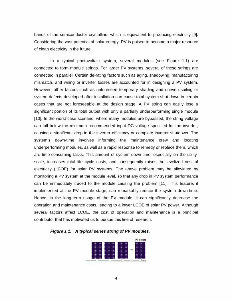
In a typical photovoltaic system, several modules (see Figure 1.1) are
connected to form module strings. For larger PV systems, several of these strings are
connected in parallel. Certain de-rating factors such as aging, shadowing, manufacturing
mismatch, and wiring or inverter losses are accounted for in designing a PV system.
However, other factors such as unforeseen temporary shading and uneven soiling or
system defects developed after installation can cause total system shut down in certain
cases that are not foreseeable at the design stage. A PV string can easily lose a
significant portion of its total output with only a partially underperforming single module
[10]. In the worst-case scenario, where many modules are bypassed, the string voltage
can fall below the minimum recommended input DC voltage specified for the inverter,
causing a significant drop in the inverter efficiency or complete inverter shutdown. The
system’s down-time involves informing the maintenance crew and locating
underperforming modules, as well as a rapid response to remedy or replace them, which
are time-consuming tasks. This amount of system down-time, especially on the utility-
scale, increases total life cycle costs, and consequently raises the levelized cost of
electricity (LCOE) for solar PV systems. The above problem may be alleviated by
monitoring a PV system at the module level, so that any drop in PV system performance
can be immediately traced to the module causing the problem [11]. This feature, if
implemented at the PV module stage, can remarkably reduce the system down-time.
Hence, in the long-term usage of the PV module, it can significantly decrease the
operation and maintenance costs, leading to a lower LCOE of solar PV power. Although
several factors affect LCOE, the cost of operation and maintenance is a principal
contributor that has motivated us to pursue this line of research.
Figure 1.1: A typical series string of PV modules.
5
To implement a PV module monitoring system at the module level, module level
voltage and current sensing are required in the form of a hardware unit that can be
inserted into the junction box of each PV panel. However, this hardware requires
communication with a central station to report the status of the PV module. To this end,
a promising candidate that can offer a cost-effective communication system is modern
wireless technology. A wireless-enabled embedded system can offer local processing
(e.g. voltage and current sensing) and communication needs. There exist several
wireless technologies to be utilized as an appropriate candidate for PV module
monitoring, as discussed in Chapter 2.
1.2. Electric Power Demand and Energy-Efficient Systems in Buildings
Transportation, manufacturing, heating, cooling, lighting, and many other needs
in modern society rely on electricity. The consumption factors that determine electric
power demand differ in geography, climate, and application types. Regardless of these
factors, buildings are one of the main contributors to energy consumption which should
be considered in energy-efficient systems. Achieving energy conservation in buildings
depends on how well the demand is managed while meeting requirements such as
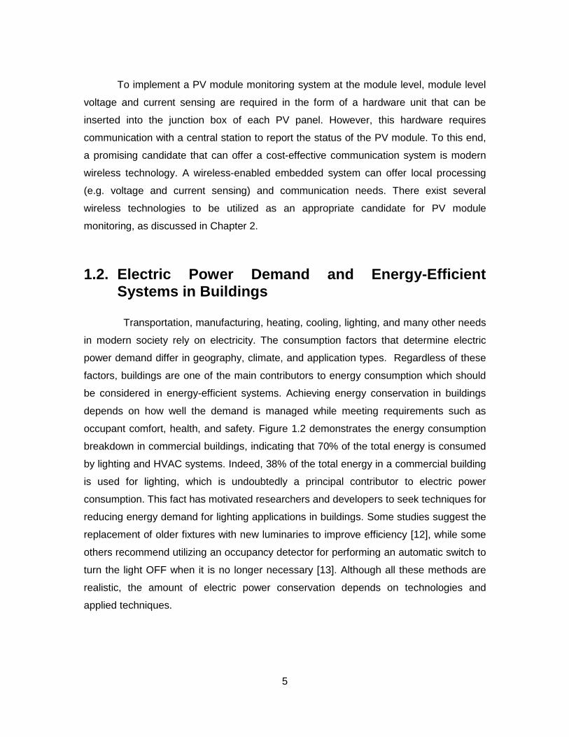
occupant comfort, health, and safety. Figure 1.2 demonstrates the energy consumption
breakdown in commercial buildings, indicating that 70% of the total energy is consumed
by lighting and HVAC systems. Indeed, 38% of the total energy in a commercial building
is used for lighting, which is undoubtedly a principal contributor to electric power
consumption. This fact has motivated researchers and developers to seek techniques for
reducing energy demand for lighting applications in buildings. Some studies suggest the
replacement of older fixtures with new luminaries to improve efficiency [12], while some
others recommend utilizing an occupancy detector for performing an automatic switch to
turn the light OFF when it is no longer necessary [13]. Although all these methods are
realistic, the amount of electric power conservation depends on technologies and
applied techniques.

6
Figure 1.2: Energy consumption breakdown in commercial buildings.
[Source: U.S. Energy Information Administration (EIA)]
Among efficient lighting technologies, fluorescent and compact fluorescent
lamps (CFL) have been employed for several decades to replace inefficient
incandescent lighting lamps. However, there is a great potential for energy efficiency
using new technologies and control mechanisms. For example, solid-state lighting
technology has been newly introduced in the form of state-of-the-art LED lighting
solutions with higher luminous efficacy in comparison with incandescent, florescent or
CFL lighting, albeit with lower power consumption [14]. The LED is controllable using DC
current drive and allows for a dimming mechanism and daylight harvesting. These
features, combined with an intelligent controller, have the capacity to achieve highly
efficient lighting solutions for buildings. Although such a system in new buildings can be
considered in the design phase, retrofitting current lighting systems is a challenging task
due to the amount of the wiring involved. Short-range wireless technologies are well-
known solutions for wiring replacement that are widely employed in building applications.
However, robustness, reliability, and power drive are some of the main concerns in
wireless applications that motivated researchers into these subjects. The second part of
the proposed research (see Chapter 4) utilizes newly introduced wireless connectivity,
featuring ultra-low power consumption technology in order to design and implement an
energy-efficient lighting system using LED lighting technology.
7
1.3. Thesis Organization
The rest of this thesis is organized as follows. In Chapter 2, we address several
different wireless technologies including local area networks (LANs) and personal area
networks (PANs) that are potential candidates for employment in renewable energy and
energy efficiency applications. Considering a wide range of brand-based features that
are added to wireless technologies, all data and tables in this chapter are extracted from
the most reliable references (e.g., IEEE 802.11 standard for Wi-Fi technology). Chapter
3 presents the design of an embedded wireless system for installation on a PV module
and its user interface that can perform current, voltage, and power monitoring system
using the ZigBee wireless technology. A proof-of-concept system is built and
experimental results are discussed in this chapter. In Chapter 4, Bluetooth low energy
technology is utilized to design, implement, and develop an energy-efficient LED lighting
system. A testbed is developed for a proof-of-concept 150W LED lighting system.
Chapter 5 provides concluding remarks and directions for future research.

8
2. Chapter 2: Wireless Embedded Systems
Nowadays, wireless technologies have widely permeated all aspects of human
life. Personal area network (PAN) [15] and wireless body area network (WBAN) [16] are
some examples of short-range wireless applications. However, the diversity of usage
cases has created a variety of wireless standards such as Z-wave, Wi-Fi, and Bluetooth
[17]-[18]. Table 2.1 illustrates a comparison between several well-known wireless
technologies: Wi-Fi [19], Bluetooth [20], Bluetooth low energy (BLE) [20], ZigBee [21], Z-
Wave [22], and ANT+ [23]. Although each standard has several versions (e.g. Wi-Fi has
IEEE 802.11a, b, g, and n), the most popular types are considered for this comparison.
Wi-Fi is mainly applicable in wireless local area networks (WLAN), and provides secure
connectivity at high speed and over a medium range. However, as indicated in Table
2.1, several other standards have been developed in the PAN and WBAN applications,
which have low data volume, short range, and low power characteristics.
Table 2.1: Typical short-range wireless standards comparison table
Wireless
Standards Wi-Fi[19] Bluetooth[20] BLE[20] ZigBee[21] Z-Wave [22] ANT+[23]
Bandwidth Up to 54Mbps 1-3Mbps 1Mbps 256Kbps 40Kbps 1Mbps
Range >100m <100m <30m <100m <30m <30m
Topology P2P, Star
Tree, Mesh
P2P
Star
P2P
Star
P2P, Star
Tree, Mesh Mesh
P2P,
Tree, Mesh
Security High High High Medium High High
Current
Consumption High Medium
Ultra-
Low Low Low
Ultra-
Low
Frequency
hopping No Yes Yes No No No
Cost High Medium Very low Low Low Very low
Note. The most popular type or version of each standard is listed in this table.

9
2.1. Wi-Fi
Wireless Fidelity (Wi-Fi) is a generic term that refers to the IEEE 802.11
communications standard, and was originally introduced in 1997 [19]. During the last
decade, it has become one of the common standards in wireless-enabled devices such
as computers, smartphones, peripheral devices, and network components [18]. The
plug-and-play capability, high speed, and medium propagation range along with
supporting several network topologies (e.g. star, tree, and peer-to-peer) make Wi-Fi a
unique solution for wireless local area networks. A summary of the typical Wi-Fi standard
is illustrated in Table 2.2. However, the new IEEE 802.11 standard versions have been
improved in some aspects such as maximum signal rate and security.
Table 2.2: Wi-Fi standard specification (Taken from [19])
Specification state
Frequency band 2.4GHz and 5GHz
Coexistence mechanism Transmit power control
Multiplexing DSSS, CCK, OFDM
Future multiplexing MIMO
Noise adaptation Physical layer
Typical output power 30-100mW (15-20dBm)
Nominal range 100m
Maximum one-way data rate 31.3Mbps
Basic cell BSS
Extension of the basic cell ESS
Topologies peer-to-peer, star, tree, mesh
Maximum number of devices in the basic cell
Unlimited in ad hoc network (IBSS); up to 2007 devices in the infrastructure networks.
Maximum signal rate 54Mbps
Channel access method Distributed: CSMA/CA
Channel efficiency Decreasing with offered traffic
Data protection 32-bit CRC
Procedures used for the network setup
Ad hoc networks: scan, authentication
Infrastructure: scan, authentication, association

10
Authentication Shared secret, challenge-response
Power save mode Doze
Wi-Fi Protocol Stack 2.1.1.
Although the upper layer in the IEEE 802.11 protocol stack is model-dependent,
the main layers, including physical (PHY), medium access control (MAC) and logical link
control (LLC) layers are permanent in the Wi-Fi firmware. Figure 2.1 demonstrates the
IEEE 802.11 protocol stack versus OSI and TCP/IP models [19]-[24].
Figure 2.1: IEEE 802.11 protocol stack vs. OSI and TCP/IP models (Taken from [19])
Wi-Fi MAC Frame Format 2.1.2.
The IEEE 802.11 general MAC frame (see Figure 2.2) consists of a MAC header,
the frame body (i.e., payload), and a frame check sequence (i.e., CRC32) [19].
Figure 2.2: IEEE 802.11 MAC frame format (Taken from [19])

11
Wi-Fi Network Topologies 2.1.3.
The Wi-Fi standard supports the independent basic service set (IBSS) and
extended service set (ESS) in the form of logical architecture as well as peer-to-peer,
star, tree, and mesh, known as physical network topologies. The main components of
logical architecture consist of a station (STA), wireless access point (AP), basic service
set (BSS), and distribution system (DS). With regard to the network topology, IEEE
802.11 has defined two operating modes, infrastructure and ad hoc (see Figure 2.3), to
deploy several physical network topologies.
Figure 2.3: Wi-Fi network topologies (Taken from [19])
2.2. Bluetooth
Bluetooth is an open proprietary wireless technology based on the IEEE 802.15.1
standard for short-range wireless communication between several devices in the
industrial, scientific, and medical (ISM) band at 2400 MHz to 2485 MHz radio
frequencies [20]. It was originally created by Ericson4 in 1994 in order to provide a
wireless alternative to the RS232 serial communication. Bluetooth technology utilizes the
adaptive frequency hopping (AFH) technique to take advantage of available frequency in
the shared 2.4GHz spectrum and to diminish the interference of other wireless
technologies in this band. The AFH technique not only acts as a robust communication
feature for Bluetooth, but also makes possible the coexistence of other wireless
4 http://www.ericsson.com/

12
technologies in electronic devices such as laptops and smartphones. Although this
standard was introduced by versions 1.0 and 1.0B, the core specification version 1.1 is
known as the first successful Bluetooth standard as it corrected earlier versions’ bugs
and problems. However, Bluetooth core 1.2 was developed in order to enhance the
transmitting/receiving speed and to support the hardware controller interface (HCI) for a
three-wire universal asynchronous receiver and transmitter (UART). Afterwards, the
Bluetooth standard developed core specification versions 2.0, 2.1+EDR, 3.0 and 4.05,
and adapted its capabilities to become a main part of PANs. The Bluetooth propagation
range is mandated by power class radios 1, 2, and 3 for 1, 10, and 100 meters
respectively. Table 2.3 demonstrates the specification of Bluetooth core version
2.1+EDR.
Table 2.3: Typical Bluetooth standard (Taken from [20])
Core version 2.1 + EDR
Frequency band 2.4-2.485GHz ISM band
Coexistence mechanism Adaptive frequency hopping
Multiplexing FHSS
Future multiplexing UWB
Noise adaptation Link layer
Typical output power Class 1=100mW (20dBm), Class 2=2.5mW (4dBm), Class 3=1mW (0dBm)
Operating range Class 1=100m, Class 2=10m, Class 3=1m
Maximum one-way data rate 2.1Mbps
Basic cell Piconet
Extension of the basic cell Scatternet
Topologies Peer-to-peer, star
Maximum number of devices in the basic cell
8 active devices and 255 in park mode
Maximum signal rate 3Mbps
5 The newest version of the Bluetooth family, core 4.0, is known as Bluetooth low energy and it is
scholarly discussed in this thesis.
13
Channel access method Centralized: TDMA
Channel efficiency Constant
Data protection 16-bit CRC (ACL links only)
Procedures used for the network setup Inquiry, Page
Authentication Shared secret, Pairing
Power save mode Sniff, Hold, Park, Standby
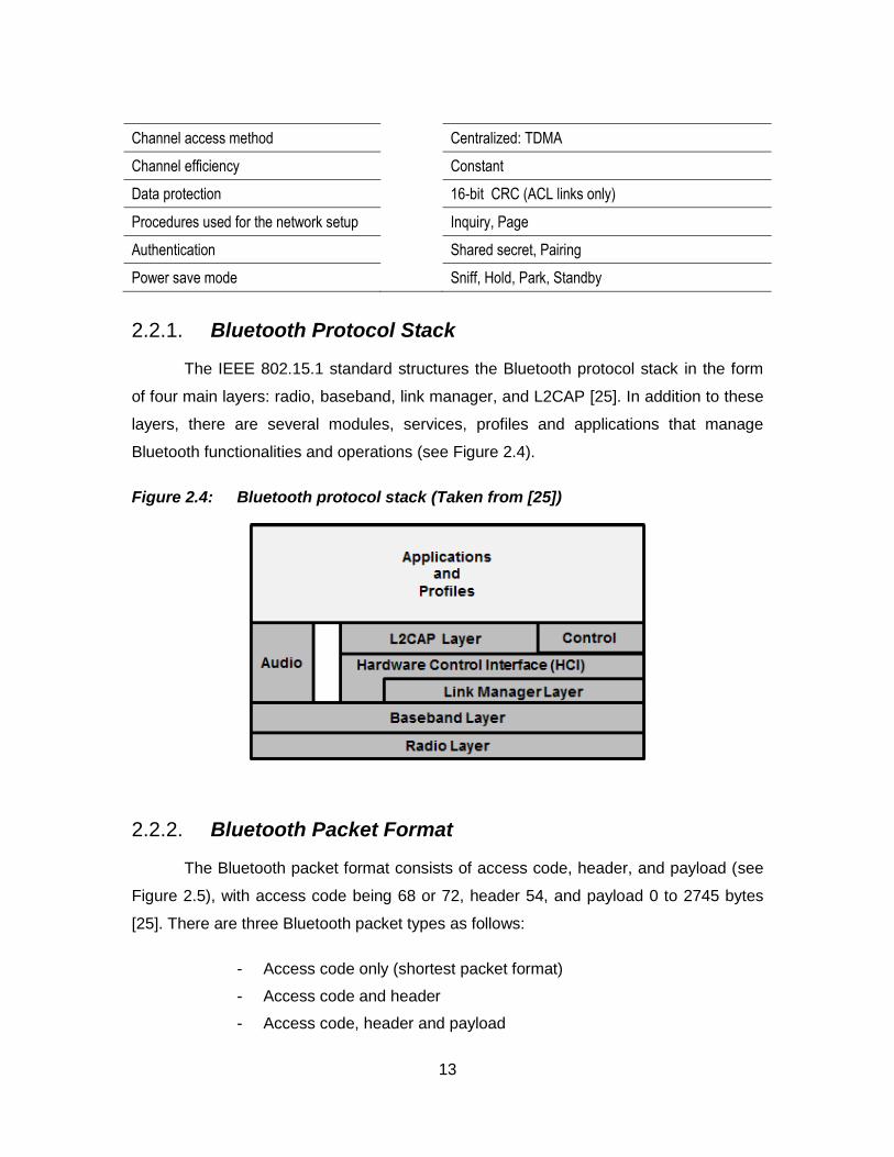
Bluetooth Protocol Stack 2.2.1.
The IEEE 802.15.1 standard structures the Bluetooth protocol stack in the form
of four main layers: radio, baseband, link manager, and L2CAP [25]. In addition to these
layers, there are several modules, services, profiles and applications that manage
Bluetooth functionalities and operations (see Figure 2.4).
Figure 2.4: Bluetooth protocol stack (Taken from [25])
Bluetooth Packet Format 2.2.2.
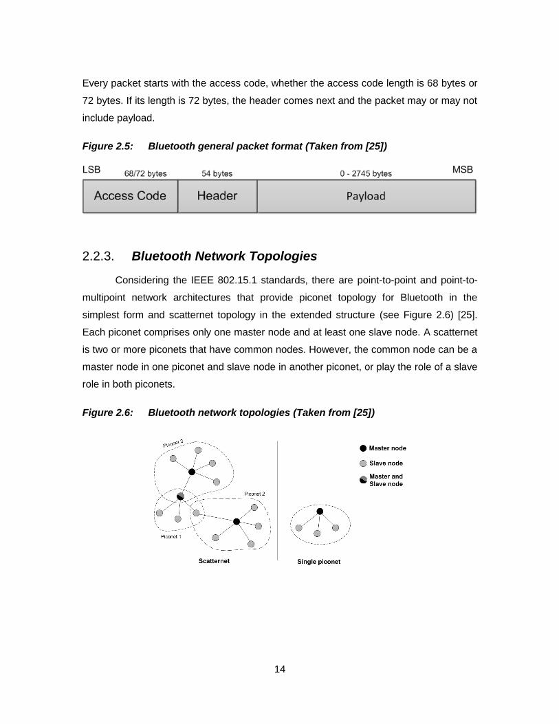
The Bluetooth packet format consists of access code, header, and payload (see
Figure 2.5), with access code being 68 or 72, header 54, and payload 0 to 2745 bytes
[25]. There are three Bluetooth packet types as follows:
- Access code only (shortest packet format)
- Access code and header
- Access code, header and payload
14
Every packet starts with the access code, whether the access code length is 68 bytes or
72 bytes. If its length is 72 bytes, the header comes next and the packet may or may not
include payload.
Figure 2.5: Bluetooth general packet format (Taken from [25])
Bluetooth Network Topologies 2.2.3.
Considering the IEEE 802.15.1 standards, there are point-to-point and point-to-
multipoint network architectures that provide piconet topology for Bluetooth in the
simplest form and scatternet topology in the extended structure (see Figure 2.6) [25].
Each piconet comprises only one master node and at least one slave node. A scatternet
is two or more piconets that have common nodes. However, the common node can be a
master node in one piconet and slave node in another piconet, or play the role of a slave
role in both piconets.
Figure 2.6: Bluetooth network topologies (Taken from [25])

15
2.3. Bluetooth Low Energy
Bluetooth low energy6 is a feature of Bluetooth core specification version 4.0,
aiming for ultra-low peak, average, and idle mode power consumption as well as low
cost. Bluetooth SIG introduced BLE in 2009 to facilitate a wide range of applications in
home automation, healthcare, security, home entertainment, fitness, and sports. Table
2.4 presents typical specifications of the Bluetooth low energy protocol [20].
Table 2.4: Bluetooth low energy (Taken from [20])
Core version 4.0
Frequency band 2.4-2.485GHz ISM band
Coexistence mechanism Adaptive frequency hopping
Modulation GFSK
Noise adaptation Link layer
Typical output power Min= 0.01mW (-20dBm) , Max= 10mW (+10dBm)
Operating range Max=100m (+10dBm)
Maximum one throughput 256Kbps
Basic cell Star (Master-Slaves)
Extension of the basic cell Star-Bus
Topologies Peer-to-peer, star
Maximum number of devices in the basic cell Unlimited
Maximum signal rate 1Mbps
Channel access method TDMA, FDMA
Data protection AES-128
Authentication Secure simple pairing
Power save mode Standby
6 Although BLE is produced in single and dual modes, the purpose of BLE in this thesis is single-
mode Bluetooth low energy and thus it is simply referred to as BLE.

16
BLE Protocol Stack 2.3.1.
The BLE protocol stack employs the low energy profile in order to consume as
low energy as possible during the operation. Figure 2.7 illustrates that the BLE protocol
stack, unlike the Bluetooth standard, does not have any audio capability. The BLE
protocol stack layers are described as follows [26]:
- The Physical Layer (PHY): transmits and receives GFSK packets
over the physical channel at 1Mbps on the 2.4GHz ISM band.
- The Link Layer (LL): controls the RF states of the transceiver
consisting of advertising, scanning, initiating, connected, or standing
by states.
- The Host-Controller Interface (HCI): processes all communications
between the host and controller, usually by SPI, USB, or a UART.
- The L2CAP: provides data encapsulation services, traffic
management, controls the order of submission of protocol data unit to
the baseband and ensures QoS access to the physical channel.
- The Attribute Protocol (ATT): allows a device to expose a specific
data format known as attributes to another device. The device
exposing attributes is introduced as server and the other is referred to
as client.
- The Security Manager (SM): generates, manages, and stores
encryption and identity keys to enable two devices to communicate
securely over a dedicated L2CAP channel. Bluetooth Low Energy
uses 128-bit AES encryption with counter mode CBC-MAC and a
user-defined application layer.
- The Generic Attribute Profile (GATT): defines the sub-procedures
for using ATT and specifies the structure of Bluetooth profiles.
- The Generic Access Profile (GAP): block provides the interface
between the application and Bluetooth profiles and handles device
discovery, connection, and services, including security procedures.

17
Figure 2.7: Bluetooth low energy protocol stack (Taken from [27])
BLE Packet Format 2.3.2.
The BLE link layer has only one packet format for both advertising and data
packet channels. Figure 2.8 illustrates this packet format, which constitutes preamble,
access address, PDU, and CRC fields, with preamble, access address and CRC having
a constant length of 1, 4, and 3 octets respectively. In contrast, PUD is variable between
2 and 39 octets [27].
Figure 2.8: Bluetooth low energy packet format (Taken from [27])
BLE Operation States 2.3.3.
Bluetooth low energy operates under five state machines, consisting of standby,
advertising, scanning, initiating, and connection (see Figure 2.9). These states facilitate
four roles in the GAP layer for a BLE device as follows [27]:
- Broadcaster: an advertiser that is non-connectable.
- Observer: scans for advertisements, but cannot initiate connections.

18
- Peripheral: an advertiser that is connectable. This device is called
slave after connection.
- Central: scans for advertisements and initiates connections. This
device is called master after connection.
Although each BLE device is able to have a certain combination of multiple roles,
it is only allowed to play one of these roles at each time instant.
Figure 2.9: State machine diagram of the BLE operation states (Taken from [27])
BLE Network Topologies 2.3.4.
The BLE protocol supports peer-to-peer and star network topologies containing
only one master and one or more slave devices (see Figure 2.10). The master node
initiates connection, and each branch device that accepts the connection is a slave
node. The Bluetooth low energy technology uses a 32-bit access address on every
packet for each slave and theoretically allows billions of devices to be connected.
However, in practice, there are some issues such as memory and inter-piconet
interference that limit the maximum number of nodes in a piconet [28].

19
Figure 2.10: BLE network topology (Taken from [27])
2.4. ZigBee
The ZigBee specification is a wireless standard for WPAN according to IEEE
802.15.4 that operates in both 2.4GHz ISM and sub-gigahertz 868/915MHz frequency
bands [21]. The first approach to creating ZigBee took place in 1998; however, the
ZigBee alliance began building the ZigBee specification on top of the IEEE 802.15.4
standard in 2003 and announced the first version of ZigBee in 2004. In contrast to
Bluetooth and BLE, ZigBee is able to support mesh network topology. Table illustrates
the specification of a typical ZigBee standard version 2007.
Table 2.5: Typical ZigBee specification (Taken from [21])
version 2007
Frequency band 2.4GHz ISM band and 868/915MHz sub-gigahertz
Modulation OQPSK and BPSK for 2.4GHz and 868/915MHz respectively
Typical output power Min= 1mW (0dBm), Max= 100mW (+20dBm)
Operating range Max=+100m (+20dBm)
Throughput 256Kbps (2.4GHz), 40Kbps (915MHz), 20Kbps (868MHz)
Topologies Peer-to-peer, star, tree, mesh
Maximum number of devices in the network
65000+
Channel access method CSMA-CA
Data protection AES-128
Authentication CBC-MAC
Power save mode Standby

20
ZigBee Protocol Stack 2.4.1.
The ZigBee protocol stack is designed based on the IEEE 802.15.4 standard and
is built on a PHY and MAC layer foundation (see Figure 2.11). This protocol stack
consists of the network (NWK) layer and framework for the application layer. The
application layer framework comprises an application support sub-layer (APS) and
ZigBee device object (ZDO) [21].
Figure 2.11: ZigBee protocol stack (Taken from [21])
ZigBee Frame Format 2.4.2.
The ZigBee frame format is defined based on the IEEE 802.15.4 PHY layer and
MAC sub-layer data frame [21]. Figure 2.12 illustrates ZigBee frames containing NWK
and APS in which NWK frames are formed in the MAC sub-layer payload. The NWK
frame has two parts, NWK payload, and NWK header (HDR). The NWK payload is
utilized for the APS frame and HDR provides network-level addressing and control
information. However, the APS frame is formed by applications and facilitates tasks such
as application-level addressing, control information, and the security mechanism [29].

21
Figure 2.12: ZigBee frame format (Taken from [21])
ZigBee network topology 2.4.3.
The IEEE 802.15.4 supports star and peer-to-peer network topologies and
performs the required structures for the ZigBee NWK layer to be designed for providing
star, tree and mesh network topologies [21]. The ZigBee standard is composed of
several device types including ZigBee coordinator, router, and end device. Regarding
network topology, all or some of these devices exist in the network. In the star topology,
a single ZigBee coordinator node manages the network and all other nodes the end
devices. However, the mesh and tree topologies, in addition to these two devices, utilize
the ZigBee router in order to extend the network (see Figure 2.13). Indeed, a cluster tree
network consists of a number of connected star networks whose central nodes are also
in direct communication with the single ZigBee coordinator. Considering a set of routers
and a single coordinator, the network is formed into an interconnected mesh of routers
and end nodes that pass information from node to node using the most cost-effective
path. If any individual router becomes inaccessible, an alternate router can be
discovered automatically and transfer network traffic.

22
Figure 2.13: ZigBee network topologies (Taken from [21])
2.5. Z-wave
Z-Wave is a proprietary short-range wireless communication protocol that
operates in the sub-gigahertz radio frequency band around 900MHz. It supports mesh
network topology with a maximum of 232 nodes [22]. Z-Wave technology is created to
provide wireless-enabled consumer electronic products for home automation. The Z-
Wave protocol stack consists of RF media, MAC, transfer, routing and application layers.
Figure 2.14 demonstrates the Z-Wave MAC frame format.
Figure 2.14: Z-Wave MAC frame format (Taken from [22])

23
2.6. ANT+
ANT is a proprietary wireless communication technology working in the 2.4GHz
ISM radio frequency spectrum created by Dynastream Innovations Inc.7 for PANs. ANT+
is an inter-protocol added to ANT technology in order to facilitate data collection and
routing in the managed network [23]. It is able to support peer-to-peer, star, tree and
mesh network topologies with over 65000 nodes. Moreover, it benefits from ultra-low
power consumption technology that is ideal for wireless sensor networks. The ANT+
protocol stack consists of radio, protocol, and user defined layers. Figure 2.15 illustrates
a comparison between ANT+ protocol and OSI models.
Figure 2.15: ANT+ technology model vs. OSI model (Taken from [23])
7 http://www.dynastream.com/

24
3. Chapter 3: PV Module Performance Monitoring System Using ZigBee Technology
Various studies have shown that a significant reduction in output power and
degradation of the performance of maximum power point trackers (MPPT) are possible
under non-ideal conditions [30]. Finding the faulty or malfunctioning PV modules can
significantly increase the system down-time of a solar PV power plant and consequently
its LCOE rises. Hence, monitoring and detection of non-ideal conditions is a critical issue
in PV modules. Several studies have been conducted in the area of PV module
performance monitoring system. For example, using a reference solar cell in PV module
performance monitoring was studied in [31], but it has a main drawback due to the cost
of the required additional PV module.
In this chapter, the concept of a solar photovoltaic (PV) performance monitoring
system is introduced by utilizing a ZigBee wireless embedded system that is inside the
junction box of the module. The proposed system is able to monitor the performance of
PV panels to detect non-ideal operating conditions. ZigBee wireless technology has
been selected in this application because of its features in terms of low cost, capability to
be used in a mesh network topology, low power consumption, and small form factor (see
Table 2.1). The mesh network topology can not only covers a wide area of PV modules
distributed in a solar PV power plant but also facilitates deployment of a redundant data
communication network between PV modules and a central monitoring system.
Moreover, ZigBee technology operates in low power conditions that make it possible to
build low power consumption wireless devices. This is essential for a high performance
PV module performance monitoring system because the PV module has to supply the
power drive of the added circuit. On the other hand, the ZigBee module can be built with
a low cost ZigBee-enabled microcontroller and a few extra components that provide a
small form factor and low cost device to be installed in the PV module junction box. In
summary, the work performed consists of the design and development of a low-cost
small form factor electronic hardware embedded module using a ZigBee-enabled

25
microcontroller. The embedded system software comprises a back-end embedded
program and front-end graphical user interface (GUI) that are developed to perform
remote monitoring of voltage, current, and power for an array of PV modules. The results
of implementation on a proof-of-concept test-bed consisting of two embedded controllers
installed on two PV modules are presented in this chapter. The experimental results
indicate that the proposed system can provide a low-cost and reliable performance
monitoring system for possible utilization in PV power plants.
3.1. System design
The design procedure consists of separating the desired system into two main
components: hardware and software with each component divided into several other
modules. In the following, we discuss these separately to gain a comprehensive
understanding of the entire system. Figure3.1 illustrates the embedded hardware blocks
to be utilized for monitoring the PV unit using a ZigBee wireless network utilizing a star
topology comprised of a remote device and central station. The remote device
addresses a PV module that is equipped with an end device (ED) and sensing devices.
The end device provides ZigBee wireless connectivity as well as local process for the PV
module’s current and voltage sensing, respectively. A step-down DC-to-DC voltage
converter that converts the DC voltage of the PV module to a 3.3V DC voltage provides
the power to drive the embedded device inside the PV module. On the other side, the
coordinator and host PC constitute the central station. Both the ED and coordinator
employ a ZigBee-enabled system-on-chip (SoC) in order to perform over-the-air
communication between the remote device and a central station. The coordinator
facilitates data flow between the ED and host PC in the central station. The host PC is
equipped with a graphical user interface (GUI) developed by NI LabView environment8 in
order to carry out real-time performance monitoring of PV modules. The system design
consists of the several components described below:
8 NI LabView: http://www.ni.com/labview

26
Figure 3.1: PV module performance monitoring system block diagram
Hardware components 3.1.1.
The hardware components of the embedded computing system include an end
device, voltage sensing, current sensing, a step-down DC-to-DC voltage converter, and
the coordinator, as described in detail in the following:
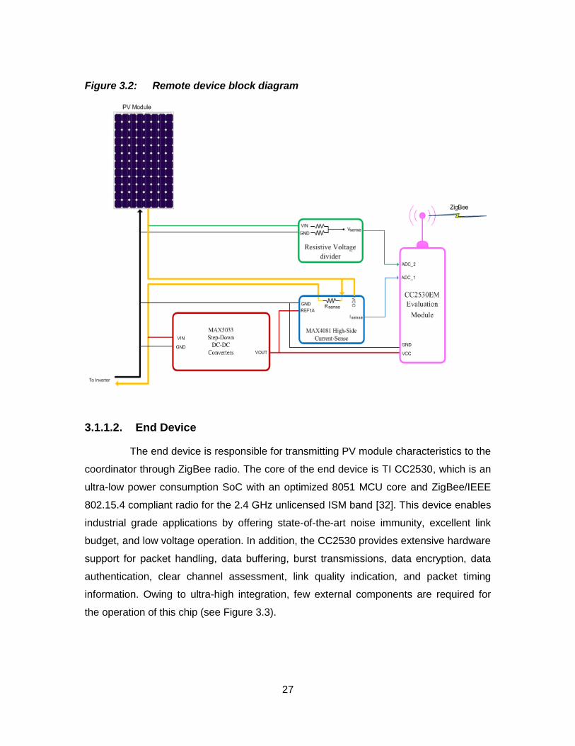
3.1.1.1. Remote Device
Figure 3.2 illustrates the block diagram of the remote device and the connection
between its components. The resistive voltage divider and high-side current-sense
amplifier measure the voltage and current of the PV module, respectively, and deliver
those values to the analog-to-digital converter (ADC) port of SoC. The step-down DC-to-
DC voltage converter acts as the power driver for the end device and current sensing
circuit.
27
Figure 3.2: Remote device block diagram
3.1.1.2. End Device
The end device is responsible for transmitting PV module characteristics to the
coordinator through ZigBee radio. The core of the end device is TI CC2530, which is an
ultra-low power consumption SoC with an optimized 8051 MCU core and ZigBee/IEEE
802.15.4 compliant radio for the 2.4 GHz unlicensed ISM band [32]. This device enables
industrial grade applications by offering state-of-the-art noise immunity, excellent link
budget, and low voltage operation. In addition, the CC2530 provides extensive hardware
support for packet handling, data buffering, burst transmissions, data encryption, data
authentication, clear channel assessment, link quality indication, and packet timing
information. Owing to ultra-high integration, few external components are required for
the operation of this chip (see Figure 3.3).

28
Figure 3.3: TI CC2530 SoC typical circuit
The CC2530 has 21 general-purpose I/O pins (19× 4 mA, 2× 20 mA) and 8
channels of these I/O pins can be programmed to perform 14-bit analog-to-digital
conversion with up to 12 bits effective number of bits (ENOB). Moreover, the reference
voltage of these ADCs are selectable as internal, external single-ended, external-
differential, or AVDD5 [32]. Having an accurate step-down DC-to-DC converter makes
AVDD5 a suitable reference voltage for this design (see Appendix A). These features
were utilized to convert analog output voltage of the current and voltage sensing circuits.
In this project, a CC2530EM evaluation module (see Figure 3.4a) was used to
avoid wasting time on CC2530 circuit fabrication. This module contains the RF IC and
necessary external components and matching filters for getting the most out of the radio
[33]. The module can be plugged into the SmartRF05EB for purposes of CC2530
programming and debugging. The SmartRF05EB (see Figure 3.4.b) is a platform for

29
evaluation modules (EM) and can be connected to the PC via USB to control the
evaluation modules [34]. In addition, the System-on-Chip Battery Board (SoC-BB) [35] is
utilized in order to facilitate connection between CC2530EM and other hardware in the
remote device.
Figure 3.4: The CC2530EM evaluation module (a) and SmartRF05EB evaluation board (b)
3.1.1.3. Current Sensing Circuit
The MAX4081 was employed to measure the PV module current, which is
essentially a bidirectional high-side current-sense amplifier [36]. It features a 4.5VDC to
76VDC input common-mode range in three gain versions, 5V/V, 20V/V, and 60V/V (see
Appendix B). This feature allows the monitoring of current output of a PV module with
voltage fluctuations as low as 4.5V. Furthermore, it features high-side current sensing at
voltages greater than the supply voltage (VCC). The MAX4081 monitors current through
a current-sense resistor and amplifies the voltage across the resistor. The 76V input
voltage range of the MAX4081 applies independently to both supply voltage (VCC) and
common-mode, input-sense voltage (VRS+). The MAX4081 charging current is
represented by an output voltage from VREF to VCC, while the discharge current is
given from VREF to GND. Measurements of OUT with respect to VREF yield a positive
and negative voltage during charge and discharge. Figure 3.5 illustrates how the current
sensing circuit is connected to other modules in the remote device.

30
Figure 3.5: Current sensing circuit for the PV module
Ideally, the maximum load current results in a full-scale sense voltage across
the current-sense resistor given by,
(3.1)
where is the full-scale sense voltage ( , and
for gains 5V/V, 20V/V, and 60V/V, respectively) and is the voltage gain of the device.
Considering a 20V/V gain and 10mΩ current sense resistor in this design, the maximum
is 2.5V.
3.1.1.4. Voltage Sensing Circuit
Considering the DC signal of a PV module and high input impedance of the
analog to digital converter (ADC_2) in the CC2530, a simple voltage divider circuit
consisting of two resistors in series is appropriate for a voltage sensing circuit. The
resistors should be arranged to have the maximum voltage equal to 3.3VDC for
application to the CC2530 analog to digital converter channels. Hence, the voltage
divider formula for the voltage sensing circuit is given by
(3.2)

31
where is the sensing voltage, is PV module voltage, and are
series resistors, respectively. Figure 3.6 illustrates the voltage sensing circuit in which a
PV module with a 28VDC open circuit voltage is utilized. Considering a value of 3.3VDC
for maximum and solving (3.2 for the series resistors, the values and are
obtained as 47kΩ and 6.3kΩ, respectively.
Figure 3.6: Voltage Sensing Circuit
3.1.1.5. Step-Down DC-to-DC Converter
A step-down DC-to-DC converter is needed to provide the DC power drive for
the end device and current sensing circuit. Figure 3.7 illustrates a step-down DC-to-DC
converter based on the MAX5033D chipset [37]. The MAX5033D is a high-efficiency,
high-voltage, step-down DC-to-DC converter that operates from an input voltage up to
76V and consumes only 270µA quiescent current at no load. This pulse-width modulated
(PWM) converter operates at a fixed 125 kHz switching frequency at heavy loads, and
automatically switches to pulse-skipping mode to provide low quiescent current and high
efficiency at light loads. The MAX5033D includes internal frequency compensation
simplifying circuit implementation. The device uses an internal low-on-resistance, high-
voltage, DMOS transistor to obtain high efficiency and reduce overall system cost. This
device includes under voltage lockout, cycle-by-cycle current limit, hiccup-mode output
short-circuit protection, and thermal shutdown. The MAX5033D delivers up to 500mA
output current and provides an adjustable output voltage, from 1.25V to 13.2V (see
Appendix C).

32
Both the end device and current sensing circuit operate with 3.3V DC, and
consequently the component values in Figure 3.7 are calculated to meet this need.
Moreover, the total current consumption of these circuits is less than 100mA, which is
below the MAX5033D maximum rating.
Figure 3.7: Step-down DC-to-DC converter schematic
3.1.1.6. Central Station
The central station contains a coordinator that is a fully operational ZigBee-
enabled USB dongle device, and a host PC equipped with graphical user interface (GUI)
(see Figure 3.1). The USB dongle employs a TI CC2531 SoC and facilitates data
communication between the PV panels and GUI through ZigBee connectivity (see Figure
3.8). The CC2531 is identical to the CC2530, with the addition of a built-in full speed
USB 2.0 compliant interface [32].
Considering gradual variations of voltage and current in the PV panel, the RS232
protocol is utilized for data communication between the USB dongle and host PC.
Although taking advantage of the RS232 communication tool in the NI LabView (GUI)
environment is straightforward, the plug and play features of USB connectivity simplify
operation. Hence, the coordinator performs a virtual serial protocol for communication
between the CC2531 USB dongle and LabView. For this purpose, the LabWindows/CVI

33
instrument driver development wizard is employed to create the USB to virtual RS232
serial driver.
Figure 3.8: CC2531 USB dongle
The performance of the PV module can be monitored on the host PC via a
graphical user interface that was developed using the NI LabView environment. This
GUI not only demonstrates real-time voltage and current signal levels but also provides
information on module status. Moreover, the calculated power is displayed in order to
investigate the performance of the modules.
Software design and development 3.1.2.
The embedded software developed in this work consists of back-end embedded
programs implemented on the MCU platforms CC2530 and CC2531 from Texas
Instruments and the front-end graphical user interface developed on the host PC. The
software algorithms and program details are discussed in the following sections. The
back-end embedded software was programmed using C-language by taking advantage
of the TI ZigBee protocol stack [32] and the IAR Embedded Workbench9 integrated
development environment (IDE). This IDE tool supports compiling and debugging of the
CC253x SoC family through the SmartRF05EB. Moreover, it is bundled with all the files
required for CC253x to start development, such as register definition header files, linker
9 IAR IDE: http://www.iar.com

34
command files, driver, and device description files needed for debugging and
programming.
3.1.2.1. End Device Embedded Software
The embedded software developed at the end device is responsible for all local
operations, including current and voltage sensor reading through ADC, while handling
over-the-air data communication between the remote device and central station. The
software flowchart depicted in Figure 3.9 illustrates the operation steps. Referring to this
feature, following system start up (i.e., board initialization and radio setup), a non-stop
loop undertakes the end device’s main operations. The main operations constitute PV
module voltage and current reading as well as data transfer to the coordinator.
Figure 3.9: End device software module flowchart
The analog to digital converter API for the TI CC25xx SoC software stack
protocol is a 16-bit signed integer (int16) function as follows:
int16 adcSampleSingle (uint8 reference, uint8 resolution, uint8 channel)
It consists of three 8-bit unsigned integer (uint8) input parameters and returns the
int16 conversation result for ADC. The supply voltage (i.e., AVDD=3.3V) is employed for
ADC voltage reference and the resolution is considered 10bits. However, ADC channels

35
2 and 4 are selected for PV module current and voltage conversion respectively. The
software C code for the end device is in Appendix D.1.
3.1.2.2. Coordinator Embedded Software
The coordinator embedded software performs data handling between the end
device and a host PC. Akin to end device embedded software, it begins with board
initialization and radio setup and afterwards continues with a non-stop loop that conducts
the coordinator’s main operations. Figure 3.10 represents the coordinator, which
continuously receives data from the end device over-the-air and transmits it to the GUI
USB port (i.e., USB to virtual serial port) and the host PC. The software C code for the
coordinator is provided in Appendix D.2.
Figure 3.10: Coordinator embedded software module flowchart
3.1.2.3. Graphical User Interface Software
The graphical user interface performs the monitoring and controlling tasks on the
host PC. The GUI was developed using the NI LabView environment, which displays
real-time voltage and current values along with the status of each PV module. Figure
3.11 illustrates a view of the graphical user interface flowchart with its LabView code
presented in Appendix E.

36
Figure 3.11: Graphical user interface software flowchart
3.2. System Integration
The final stage of the design involves system integration, which is accomplished
in accordance with the bottom-up design methodology by means of connecting the
individual modules constituting the remote device and central station. Figure 3.12
illustrates components of the remote device that that was utilized in the experiments. On
the central PC station, a TI CC2530 USB dongle is used. Furthermore, the software was
developed and tested by means of the IAR integrated development environment, which
was flashed into both the end device and coordinator using the SmartRF05EB
evaluation board.

37
Figure 3.12: Remote device integrated system
3.3. System Implementation and Experiment
The embedded hardware and software modules are built and integrated in order
to evaluate the performance of the PV panels. The prototype system is illustrated in
Figure 3.13, consisting of two PV modules equipped with end devices (i.e., ZigBee-
enabled end devices), a coordinator (i.e., CC3531 USB dongle), and a monitoring host
computer. This setup conducts an experiment on a proof-of-concept test bed for the
proposed research.
Figure 3.13: Experimental setup for PV module performance monitoring with two modules
In a practical system, the series connection of PV modules forms “module
strings”, which are connected to an inverter. To investigate operation of the monitoring

38
system, fault conditions due to partial shadowing were introduced by using a curtain in
the lab when the module was subjected to sunshine. Considering the PV module’s I-V
characteristic, when a shadow of about 50% was created on the PV module_1, its
current and voltage dropped, as shown in Figure 3.14. In this case, the string and PV
module_2 current is the same as that of PV module_1. Consequently, the voltage of the
second panel increases due to the I-V characteristic of PV module_2. Figure 3.14
demonstrates the output on the user interface indicating this behavior.
Figure 3.14: Voltage, current and power for two series PV modules under partial shadow represented in GUI

39
4. Chapter 4: Energy-efficient Lighting using Bluetooth Low Energy (BLE)
The concept of an energy-efficient lighting system is an attractive research area
and it is being studied nowadays. Several research studies have shown that electrical
energy use can be significantly lowered by utilizing lighting control systems such as
occupancy detectors [38], dimming technologies [39], and daylight harvesting
mechanisms [40]. For instance, an occupancy sensor with a 15-20 minute ON-time
period in an office can save 20-26% of lighting energy compared to the manual
operation of a wall switch [41]. Moreover, by utilizing a combination of daylight
harvesting and dimming techniques, additional savings of about 20% can be achieved
[41]. The percentages can vary based on the application and environment; for example,
in low-occupancy areas, energy savings result mainly from the occupancy sensors, while
in areas with high-occupancy, savings are mostly achieved by means of daylight
harvesting and dimming [41]. Thus, the appropriate energy-efficient lighting systems rely
on these techniques and control mechanisms that manage the relation between
occupancy sensors, daylight harvesting, and dimming based on the application
environment (e.g., office building, warehouse, or residential environments). However, the
controller module needs communication technologies for access to several parts of the
energy-efficient lighting system. Several researches have been conducted on wired
technologies for energy-efficient lighting systems [42]-[43], but they have some
drawbacks in terms of the cost of new cabling and installation for retrofitted buildings. To
overcome the wiring problem, wireless technologies have recently been introduced and
they are becoming more and more popular in the area of building automation and
energy-efficient applications, and so have created new research fields. For instance,
ZigBee wireless connectivity was studied in several applications for intelligent and
energy-efficient lighting systems [44]-[46]. Although ZigBee wireless technology is able
to resolve wired system problems in terms of cost and installation, it operates in the 2.4
GHz ISM radio frequency band in which Wi-Fi wireless technology is employed for

40
WLAN in buildings. Thus, ZigBee technology may have potential interference issues
when operated with Wi-Fi [47-49], which has motivated researchers to study other
emerging technologies For example, in [47] the authors have studied the interference
between microwave ovens and WiFi transmitters and have concluded that throughput
performance can be affected due to this interference. Based on the study in [48], when
ZigBee co-exists with WLAN and Bluetooth the dominant interference source is the
WLAN.
In this chapter we discuss the design and implementation of a wireless-based
LED lighting testbed integrated with light and occupancy sensors. The system utilizes
BLE wireless modules, which can be configured to form a network for data exchange
between different components including sensors and actuators. Characteristics such
as ultra-low power consumption, along with other advantages such as small form factor,
low cost, and backward capability, make BLE an attractive technology for wireless
sensors in energy-efficient applications. Additionally, BLE uses the adaptive frequency
hopping (AFH) technique [50] in order to diminish interference of other wireless
technologies and so to achieve reasonable reliability and robustness characteristics. To
use the same programming environment tools discussed earlier in Chapter 3, the TI
CC2540 SoC was chosen for the BLE-enabled embedded system. The system software
comprises a back-end embedded program and a front-end graphical user interface (GUI)
to demonstrate the real-time LED dimming level, lighting fixture power consumption, and
the state of the motion detector. The experimental setup, consisting of a BLE-enabled
ambient light sensor, motion detector, and dimmer circuit along with a 150W high-bay
LED fixture is presented in this chapter.
4.1. System Design and Implementation
Figure 4.1 illustrates the developed BLE-enabled energy-efficient lighting system
block diagram containing a central system and BLE piconets. The central system
consists of a BLE master device and host PC equipped with a graphical user interface.
The BLE-enabled ambient light sensor, motion detector, and dimmer, as well as a LED
lighting fixture, constitute a BLE piconet. The LED fixture light level is controlled using a

41
BLE-enabled dimmer that it is programmed by means of a combination of ambient light
level and motion detector over-the-air.
Figure 4.1: BLE-enabled energy-efficient lighting system block diagram
The system is divided into two main components: hardware and software, with
each component divided into several modules. The BLE network utilizes a TI CC2540
chip that is a low-cost, low-power, true system-on-chip (SoC) for Bluetooth low
energy applications [45]. It enables robust BLE master or slave nodes to be built with
very low total bill-of-material costs. The CC2540 combines an excellent RF transceiver
with an industry-standard enhanced 8051 MCU. Indeed, CC2540 is the same as
CC2530 with the only difference at the RF transceiver stage. Consequently, all
development tools such as SmartRF05EB and IAR that were utilized for CC2530 in
Chapter 3 are applicable for CC2540 by considering the BLE stack protocol instead of
ZigBee. The CC2540 Mini Development Kit [45] is utilized to avoid time spent on PCB
and circuit fabrication. The kit contains a CC2540 USB Dongle and CC2540 Keyfob that
operate as BLE master and slave nodes respectively. The hardware and software are
discussed in detail in the following sections.
Hardware Components 4.1.1.
The piconet constitutes a BLE-enabled ambient light sensor, motion detector,
and dimmer, referred to as BLE slave nodes in this work. The CC2540 Keyfob is the
main part of these devices and handles the local process for each device and provides

42
BLE connectivity. On the other side, the central system employs a CC2540 USB dongle
as the BLE master device that it is responsible for data exchange between the piconet
devices and host PC. Thus, the hardware components considered in the design phase
are as follows.
4.1.1.1. TI CC2540 Keyfob
The TI CC2540 Keyfob [45] is a working reference design for software
development of single-mode Bluetooth low energy applications based on the TI CC2540.
It operates as a BLE peripheral device and contains modifiable software that can be
tailored toward different applications. The proposed design considers Keyfob not only to
perform the local process for each piconet device but also to be responsible for data
exchange with the BLE master device through BLE connectivity. Table 4.1 presents
CC2540 IO pins that are accessible on Keyfob header connections. The debug header
connection is used for programming and debugging purposes, but the test header
connection, in contrast, can be utilized to interface with other devices. The Keyfob power
is supplied by a 3.3V coin cell battery for the ambient light sensor and motion detector.
However, the dimmer is installed in the LED fixtures where the DC-line is accessible and
the dimmer is energized using this line.
Table 4.1: CC2540 IO pins that are accessible on Keyfob header connections
Debug
Header
pin
IO
pin
Functionality
Test
Header
Pin
IO
pin Functionality
1 - GND 1 P0_6 IO / ADC
2 - VDD 2 P1_5 IO / ADC
3 P2_2 DC 3 P0_7 IO / ADC
4 P2_1 DD 4 P1_7 IO / ADC
5 P0_4 SSN 5 P0_1 IO / ADC
6 P0_5 SCK 6 P1_4 IO / ADC
7 - RESET_N 7 P0_0 IO / ADC
8 P0_3 MOSI 8 P1_3 IO / ADC
9 - VDD 9 - -
10 P0_2 MISO 10 P1_2 IO / ADC

43
4.1.1.2. TI CC2540 USB Dongle
The TI CC2540 USB dongle [51] enables both BLE and USB connectivity that
facilitate data exchange between the host PC and piconet devices. It is similar to the
CC2531 USB dongle reviewed in Chapter 3, with the exception of the RF transceiver.
Therefore, the USB dongle operations that were explained in Section 3.1.1.6 are
applicable to the CC2540 USB dongle.
4.1.1.3. BLE-enabled Ambient Light Sensor
An ambient light sensor is used in the daylight harvesting mechanism by
employing ambient light level measurement in order to specify the dimming level of the
LED lighting. Figure 4.2 illustrates a BLE-enabled ambient light sensor schematic
diagram constituting a TI CC2540 Keyfob, Osram SFH3310 phototransistor [52], and an
amplifier stage. The SFH3310 is an ambient light silicon NPN phototransistor with V-
lambda characteristics and low output current. It is able to measure light intensity
10000lux in the full range (see Appendix F). The transistor Q1 is a single-stage bipolar
junction transistor (BJT) amplifier that performs phototransistor output signal
conditioning. The amplifier output is connected to pin 6 in IO port 0 (i.e., P0_6) of the
CC2540 that operates in the ADC mode. Consequently, the ambient light level is
converted to a digital signal that is ready to be sent to the BLE master device.
Figure 4.2: BLE-enabled ambient light sensor schematic
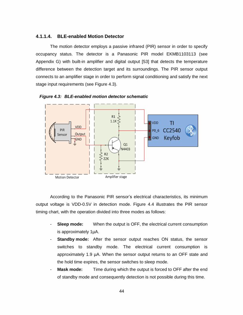
44
4.1.1.4. BLE-enabled Motion Detector
The motion detector employs a passive infrared (PIR) sensor in order to specify
occupancy status. The detector is a Panasonic PIR model EKMB1103113 (see
Appendix G) with built-in amplifier and digital output [53] that detects the temperature
difference between the detection target and its surroundings. The PIR sensor output
connects to an amplifier stage in order to perform signal conditioning and satisfy the next
stage input requirements (see Figure 4.3).
Figure 4.3: BLE-enabled motion detector schematic
According to the Panasonic PIR sensor’s electrical characteristics, its minimum
output voltage is VDD-0.5V in detection mode. Figure 4.4 illustrates the PIR sensor
timing chart, with the operation divided into three modes as follows:
- Sleep mode: When the output is OFF, the electrical current consumption
is approximately 1µA.
- Standby mode: After the sensor output reaches ON status, the sensor
switches to standby mode. The electrical current consumption is
approximately 1.9 µA. When the sensor output returns to an OFF state and
the hold time expires, the sensor switches to sleep mode.
- Mask mode: Time during which the output is forced to OFF after the end
of standby mode and consequently detection is not possible during this time.

45
The motion detector output connects to pin six in IO port zero (i.e., P0_6) of the
CC2540 that is operating in the input mode.
Figure 4.4: PIR sensor timing chart
4.1.1.5. BLE-enabled Dimmer
Energy efficiency is accomplished in LED lighting by means of a dimming
mechanism according to the combination of daylight harvesting and occupancy status. In
this design, pulse-width modulation (PWM) dimming is considered owing to its simplicity
of implementation with LED lighting; however, other techniques such as analog and
phase control dimming are applicable. In PWM dimming, the LEDs are driven with full
amplitude pulses of current and the width of the pulses is varied to control the apparent
brightness. This type of dimming relies on the capability of the human eye to integrate
the average amount of light in the pulses. Figure 4.5 illustrates a BLE-enabled dimming
schematic based on the PWM dimming technique. The TI CC2540 produces the PWM
signal and transfers it to the PWM switch through IO pin P1_7 that operates in peripheral
mode. The PWM switch constitutes Q1 MOSFET model IRFP260 [54] that benefits from
fast switching, low on-resistance and cost-effective features (see Appendix H).

46
Figure 4.5: BLE-enabled dimmer schematic
The BLE master device sends both ambient light level and occupancy status to
the BLE-enabled dimmer. The Keyfob, in the dimmer, is not only responsible for
receiving that data and calculating the dimming level but also resolves the duty cycle
and produces the PWM signal. Subsequently, the PWM signal switches ON/OFF Q1
through the MOSFT gate and decreases the forward bias current of the LED string that
dims the LED light intensity. Indeed, this mechanism cuts the supply of current for short
intervals, thereby causing the LED to turn OFF, but before the light turns completely
OFF, the current supply is established. Considering the switching frequency in the range
of hundreds, the human eye perceives the LED lighting as dimmed.
Software Design and Development 4.1.2.
The software consists of back-end embedded programs that are implemented on
the embedded platforms (i.e., TI CC2540 SoC) and the front-end graphical user interface
running on the host PC. The back-end embedded software is programmed by C code,
taking advantage of the TI Bluetooth low energy software stack [26], and was developed
by means of the IAR Embedded Workbench integrated development environment (IDE).
This IDE tool supports compiling and debugging of the CC25xx SoC family through the
SmartRF05EB. Moreover, it is bundled with all the files required for CC25xx to start
47
development, such as register definition, header files, linker command files, driver, and
device description files needed for debugging and programming.
According to the Bluetooth low energy network topology, the ambient light
sensor, motion detector, and dimmer (i.e., piconet devices) operate in slave and server
roles in the link and ATT layers respectively. On the other hand, the CC2540 USB
dongle performs master and client roles in these layers. Additionally, the TI BLE
software platform supports two different stack configurations for the BLE devices as
follows [26]:
- Single-Device: The controller, host, profiles, and application are
implemented on the CC254x as a true single chip solution.
- Network Processor: The controller and host are implemented together on
the CC254x while the profiles and application are implemented separately.
The application and profiles communicate with the CC254x by means of
vendor-specific HCI commands using a hardware or UART interface, or using
a virtual UART interface over USB.
The BLE-enabled ambient light sensor, motion detector, and dimmer were
designed and developed in single-device configuration and the BLE master device that
interfaces with the host PC is implemented in network processor configuration. In
addition to the roles and configuration, the BLE application requires some software
profiles performed in the BLE software stack or developed by Bluetooth low energy
software developers. However, the energy-efficient lighting profiles utilized in this
research consist of ambient light, motion detector, and dimmer profiles developed for the
first time.
4.1.2.1. Ambient Light Sensor Software Development
The ambient light sensor software contains the ambient light profile and is
responsible for reading the ambient light level and transferring it to the BLE master
device through the BLE connection. The ambient light level is a hexadecimal number in
the range 0x0000 to 0x2710 that represents light intensity between 0 lux and 10,000 lux
(i.e., SFH310 phototransistor operation range). Figure 4.6 illustrates the ambient light
sensor operation starting with system initialization and a non-stop loop handled by the

48
operating system abstract layer (OSAL). The OSAL is not an actual operating system
(OS) in the traditional sense, but rather a control loop that allows the software to set up
the execution of events [26].
The ambient light sensor functionality can be modeled using a state machine by
taking such roles as slave and server in the connection preparation state. After the
connection preparation phase, the state machine changes to the advertising mode and
remains in this state until connection is established. Next, it transfers to a continuance
ambient light level measurement situation that is a simple ADC read process. The state
changes to read response, whereupon a BLE read request arrives from the BLE master
device and returns to the previous state immediately after performing read response.
Both read ambient light and read response states occur in the connection mode. If, for
any reason, disconnection occurs in these steps, the state automatically transfers to the
advertising mode.
Figure 4.6: Ambient light sensor operation state machine
4.1.2.2. Motion Detector Software Development
The motion detector software contains a motion detector profile that is
responsible for determining occupancy status and transferring it to the BLE master
device through BLE connectivity. The occupancy status can be 0x8000 or 0x0000 to
represent existing and non-existing occupant conditions respectively. Figure 4.7
illustrates the operation of the motion detector state machine. This software is the same

49
as the ambient light sensor, except for reading the occupancy status state, which is a
simple logic level detection.
Figure 4.7: Motion detector operation state machine
4.1.2.3. Dimmer Software Development
The dimmer software is more complex in comparison with the previous case as
the dimmer profile needs to manage the system timer to generate the PWM signal. The
dimming level is a logical OR operation of ambient light level and occupancy status that
can be a hexadecimal number between 0x0000 and 0xA710. The BLE master device
utilizes logical OR operation to send dimming data in one cycle. TI CC2540 is equipped
with four independent programmable timers10 with timer/counter/PWM functionality. In
this design, a 300Hz PWM signal is generated by means of timer 3 that can produce the
required duty cycle for the LED lighting dimmer.
10
They contain two 16-bits (i.e., timer 1 and 2) and two 8-bits (i.e., timer 3 and 4) timers. Note that Timer 2 is for timekeeping in the BLE link layer and it must not be used by any application.

50
Figure 4.8: Dimmer operation state machine
According to the dimmer profile algorithm, the state machine will set a new
dimming level after connection is established (see Figure 4.8). In this phase, the PWM
duty cycle is computed in accordance with the ambient light level and occupancy status
that come from the BLE master device. Next, in the dim LED lighting state, the PWM
signal is generated using timer 3 and the system will remain in this stage until a write
command is requested from the BLE master device. This is the step in which new
parameters (i.e., ambient light level and occupancy status) are received and the system
state is transferred to a new dimming level. Again, if disconnection occurs, the state
changes to the advertising mode.
4.1.2.4. BLE Master Device Software Development
The BLE master device is responsible for receiving ambient light level and
occupancy status and sending them to the dimmer by means of the ATT read and write
requests, respectively. It acts as a master node in the BLE network topology, while also
sending request commands to piconet devices, and consequently operates as a client in
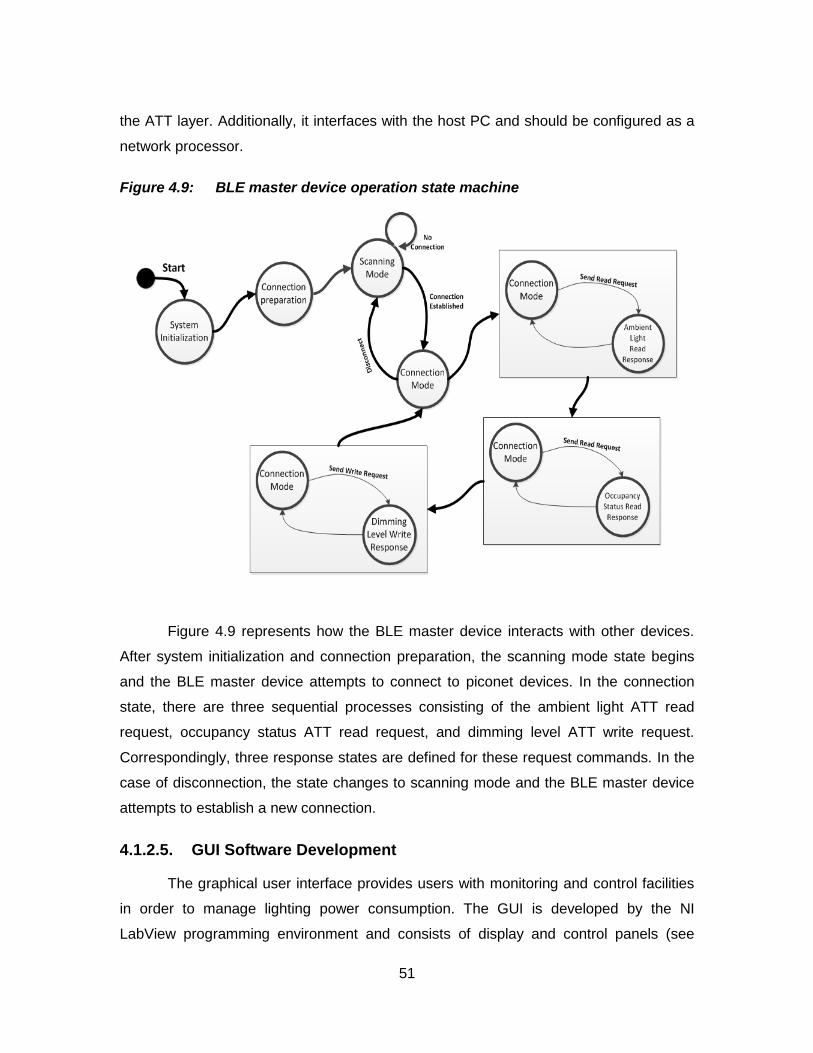
51
the ATT layer. Additionally, it interfaces with the host PC and should be configured as a
network processor.
Figure 4.9: BLE master device operation state machine
Figure 4.9 represents how the BLE master device interacts with other devices.
After system initialization and connection preparation, the scanning mode state begins
and the BLE master device attempts to connect to piconet devices. In the connection
state, there are three sequential processes consisting of the ambient light ATT read
request, occupancy status ATT read request, and dimming level ATT write request.
Correspondingly, three response states are defined for these request commands. In the
case of disconnection, the state changes to scanning mode and the BLE master device
attempts to establish a new connection.
4.1.2.5. GUI Software Development
The graphical user interface provides users with monitoring and control facilities
in order to manage lighting power consumption. The GUI is developed by the NI
LabView programming environment and consists of display and control panels (see

52
Figure 4.10). It runs on a host PC and interfaces with the BLE network through serial to
USB virtual port.
Figure 4.10: Graphical user interface
The display panel demonstrates run-time power consumption, the percentage of
the power usage, and occupancy status. The control panel facilitates manual operations
including LED lighting ON/OFF controls and manual dimming. Indeed, the control panel
grants the user permission to override automatic operation. Figure 4.11 illustrates a GUI
operation state machine that begins by serial port initialization. Depending on the mode
of operation, automatic or manual, it transfers to the next state. In the automatic
operation mode, each second the state changes to the read and display process during
which the power consumption, percentage of power usage, and occupancy status are
read and displayed. However, that data is overridden in the manual operation,
depending on the user’s decision.

53
Figure 4.11 GUI operation state machine
4.2. System Integration and Experimental Evaluation
The hardware components were individually designed and implemented, and
corresponding software for these components was developed as a part of the thesis
work performed. The proof-of-concept energy-efficient lighting system was investigated
by means of the experimental setup comprising a BLE-enabled ambient light sensor,
motion detector, LED dimmer circuits, a USB dongle, a high-power 150W LED lighting
fixture, and a host PC equipped with GUI (see Figure 4.12). This testbed is located in the
Motion and Power Electronics Control Lab at SFU. The BLE-enabled ambient light
sensor is placed in front of a window and away from the LED fixture. Moreover, the BLE-
enabled motion detector is installed in a appropriate position where it is able to
recognize the presence of occupants.

54
Figure 4.12: Experimental setup for energy-efficient intelligent lighting system using BLE
The experiment begins with automatic mode and an unoccupied condition with
the curtains down to prevent daylight from entering the lab. Consequently, the LED
lighting fixture is in the OFF state and power consumption shows a value around zero
(see Figure 4.13.a). Regardless of the ambient light level, the fixture remains OFF
pending an occupant or manual turn on. The LED lighting switches to ON with full light
level (i.e., non-existing daylight condition) immediately after an occupant is detected (see
Figure 4.13.b). In this case, maximum power is consumed and the fixture operates
inefficiently. To demonstrate daylight harvesting, the curtains were drawn back to allow
sunlight into the room, resulting in an increase in the level of the interior light level. The
ambient light sensor measures the new light intensity and transfers it to the dimmer
through the BLE connection and the BLE master device. Accordingly, the dimmer
reduces the PWM duty cycle, hence dimming the LED lighting level. The above scenario
was repeated several times, based on which the power usage percentage chart shown
in Figure 4.13.c was obtained. The Figure 4.13.c illustrates how daylight changes the
LED fixture power consumption. Indeed, a combination of daylight and artificial light
facilitates energy efficiency in the lighting system. Furthermore, the occupant can

55
manually operate the system by switching ON the system and dim the lighting through
the control panel (see Figure 4.13.d).
Figure 4.13: Experimental results for energy-efficient lighting system

56
5. Chapter 5: Concluding Remarks and Directions for Future Research
In this thesis, wireless embedded systems were studied and utilized with two
applications to renewable energy and energy efficiency. These applications addressed
two solutions for reducing total life cycle costs of solar PV electricity production and
decreasing energy consumption in buildings using an energy-efficient lighting system. To
investigate the research outcome, proof-of-concept systems consisting of prototype
devices and testbeds were implemented. Conclusions and future works for these
researches are described in the following.
5.1. PV Module Performance Monitoring System Using ZigBee Technology
Performance monitoring in a solar power plant at PV module level is crucial to
reduce the operational and maintenance costs of solar PV power systems. To attain this
objective, a controller and monitoring system comprising hardware and software is
required. On the other hand, such a system needs data communication for its operation.
To avoid the cost of extra wiring, wireless-embedded systems are able to provide
alternative solutions. Hence, a ZigBee-enabled system-on-chip was utilized for this
purpose because of its advantages in terms of low cost, mesh topology, and low power
consumption. According to the experimental results, this system is able to report real-
time conditions of PV modules that help to find underperforming PV modules and reduce
maintenance costs, and consequently decrease the total life cycle cost. The LCOE factor
is not only directly proportional to TLCC but is also in inverse proportion to total lifetime
energy production (TLEP). A popular method for increasing the TLEP of the solar PV is
maximum power point tracking technique at inverter level [55]-[56], although it has some
drawbacks such as mismatch losses between the PV panels, and MPPT power losses
as well as block diodes losses [57]. Recently, the MPPT technique at the PV module
level has motivated researchers to undertake new research in order to find cost-effective

57
solutions for this purpose [58]-[59]. However, MPPT at module level requires data
communication with a central controller module and this can be accomplished using a
wireless system. Thus, the results in this thesis can be utilized in the study of ZigBee-
enabled MPPT systems at the PV module level for future research that makes it possible
to increase TLEP by maximizing the PV module power output.
5.2. Energy-efficient Lighting Using Bluetooth Low Energy
Utilizing energy-efficient systems leads to decreasing power consumption and
energy demand. This strategy makes it possible to perform the same functions with less
electricity. This is especially important when the cost of generation of renewable energy
is high, as is the case for many sources of renewable energy such as solar, wind, and
wave power. To achieve this objective, an energy-efficient LED lighting system was
implemented using the Bluetooth low energy technology. The experimental results
demonstrate how the power consumption of an LED lighting luminaire can be decreased
using BLE-enabled ambient light and occupancy sensors and a dimmer. Although the
concept of the energy-efficient lighting system was not new, this is the first time that BLE
as an emerging technology has been studied for this purpose. The most important
research outcomes are BLE profiles for an energy-efficient lighting system that were
designed and developed for the first time. Considering the energy consumption
breakdown in commercial buildings (see Figure 1.2), it seems that expanding this
technique and acquiring a total solution for energy-efficiency in buildings requires a
general energy-efficient BLE profile, consisting of lighting, HVAC, appliances, security,
etc., and this is recommended for future work.

58
Appendices

59
Appendix A. TI CC2530 SoC

60

61
Appendix B. MAX4080/MAX4081

62
Appendix C. MAX5033D

63
Appendix D. Software C code for ZigBee-enabled solar PV power performance monitoring
D.1. End device source codes
/******************************************************************************* Filename: rf_modem_CC2530.c Description: RF Modem cc2530 is an application which reads the voltage and current of PV module and sends them to coordinator through the Zigbee radio between CC2530EM and CC2531 USB Dongle. This application implements a simple ACK handshake on top of MRFI. By: Younes Rashidi Supervised by: Prof. M. Moallem Simon Fraser University/School of Eng. Sc./Mechatronic Systems Eng. *******************************************************************************/ //--------------------- Includes ---- ---------------------------------------// #include "hal_defs.h" #include "../common/mrfi_link.h" #include "hal_board.h" #include "hal_mcu.h" #include "hal_uart.h" #include "hal_lcd.h" #include "hal_led.h" #include "hal_timer_32k.h" #include "hal_assert.h" #include "adc.h" #include "../common/cc8051/adc.h" #include "util_lcd.h" #include "stdio.h" #include "string.h" #include "math.h" //----------------------------------------------------------------------------// /******************************************************************************* * CONSTANTS and DEFINITIONS */ //------------------------- define application parameters---------------------// #define APP_PAYLOAD_LENGTH 11 #define DEVICE_1_ADDR 0x25EB #define DEVICE_2_ADDR 0x25DE #define MRFI_CHANNEL 0 #define DEVICE_1 0 #define DEVICE_2 1 #define N_RETRIES 5 //----------------------------------------------------------------------------// //----------------------- Globale variables ----------------------------------// static XDATA uint8 pTxData[APP_PAYLOAD_LENGTH]; static XDATA uint8 pRxData[APP_PAYLOAD_LENGTH]; static uint16 appRemoteAddr; static uint16 appLocalAddr; static void appRfReceiverTask(void);

64
static void appRfSenderTask(void); uint8 SendOk; //----------------------------------------------------------------------------// //------------------------------- Main Function-------------------------------// void main(void) halBoardInit(); // Initialise board peripherals. while(TRUE) // Endless loop. HAL_PROCESS(); // On-board device processing (UART etc.). appLocalAddr = DEVICE_2_ADDR; // Set local address for End Device. appRemoteAddr= DEVICE_1_ADDR; // Set remote address for coordinator. mrfiLinkInit(appLocalAddr,appRemoteAddr,MRFI_CHANNEL); // Initialise the MRFI layer. Selects RF channel and addresses. halTimer32kIntEnable(); // Enable 32KHz timer interrupt. appRfReceiverTask(); // Function for receiving data other End Devices (router role). appRfSenderTask(); // Function for read voltage/current of PV module and sending them to coordinator. if(SendOk==0x01) // If end device could not send packets to coordinator, it try send them to router (mesh topology). appLocalAddr = 0x25DF; // Set local address for End Device. appRemoteAddr= 0x25EC; // Set remote address for router. mrfiLinkInit(appLocalAddr,appRemoteAddr,MRFI_CHANNEL); // Initialise the MRFI layer. Selects RF channel and addresses. appRfSenderTask(); // function for read voltage/current of PV module and sending them t router. SendOk=0; // Clear sending flag for next loop. //------------------------------End of Main Function -------------------------// //----------- Function for receiving data from coordinator or router----------// static void appRfReceiverTask(void) uint16 l; uint8 Rf_Ready=0x00; appLocalAddr = 0x25EC; appRemoteAddr= 0x25DF; mrfiLinkInit(appLocalAddr,appRemoteAddr,MRFI_CHANNEL); // Initialise the MRFI layer. Selects RF channel and addresses. halTimer32kIntEnable(); // Enable 32KHz timer interrupt. for(l=0;l<65350;l++) //This loop creates a short delay for verifying if RF data is ready. Rf_Ready=mrfiLinkDataRdy(); //Fuction that Returns true if RF data is ready. if (Rf_Ready==0x01) break; //This condition breaks loop as long as RF data will be ready.

65
if (Rf_Ready==0x01) //If RF data is ready, read data and put them in the sending variable. mrfiLinkRecv(pRxData,0); //Function that Read data from the RX buffer. pTxData[5]=pRxData[0]; //Put received data into sending TX buffer. pTxData[6]=pRxData[1]; pTxData[7]=pRxData[2]; pTxData[8]=pRxData[3]; pTxData[9]=pRxData[4]; pTxData[10]=0x01; //Define End Device ID (ID=0,1,...,255). else //If RF data is not ready, clear sending TX buffer. pTxData[6]=0; pTxData[7]=0; pTxData[8]=0; pTxData[9]=0; pTxData[10]=0; Rf_Ready=0x00; // clear RF data ready flag for next loop. //--------------------- End of receiving function ---------------------------// //----------- Function for read voltage/current of PV module and -------------// //----------------- sending them to coordinator or router --------------------// static void appRfSenderTask(void) uint8 nBytes=0x0B; uint8 payloadLength= 0; uint8 bytesToRead= 0; bytesToRead = MIN(nBytes, APP_PAYLOAD_LENGTH); // Macro for define number of byte that it should be consider for the payload //length calculation. payloadLength+= bytesToRead; // calculate payload length. pTxData[0]=1; //Define End Device ID (ID=0,1,...,255). adcSampleSingle(0x80,0x10, 0x02); //Function that reads PV module Current from ADC channel 2. pTxData[1]=ADCH; //Put ADC Data High Byte into sending TX buffer. pTxData[2]=ADCL; //Put ADC Data low Byte into sending TX buffer. adcSampleSingle(0x80,0x10, 0x04); //Function that reads PV module voltage from ADC channel 4. pTxData[3]=ADCH; //Put ADC Data High Byte into sending TX buffer. pTxData[4]=ADCL; //Put ADC Data low Byte into sending TX buffer. SendOk=mrfiLinkSend((uint8*)pTxData, payloadLength,N_RETRIES); //Send data on the RX link. //------------------ End of sending Function ---------------------------------//
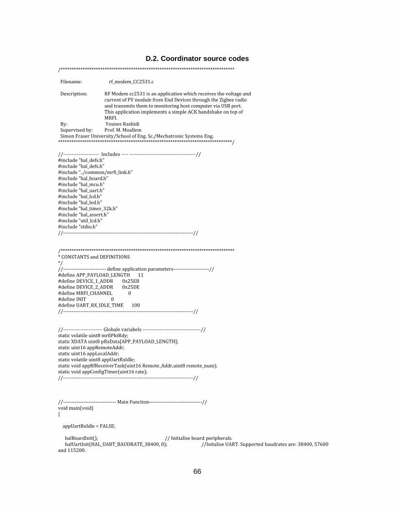
66
D.2. Coordinator source codes
/******************************************************************************* Filename: rf_modem_CC2531.c Description: RF Modem cc2531 is an application which receives the voltage and current of PV module from End Devices through the Zigbee radio and transmits them to monitoring host computer via USB port. This application implements a simple ACK handshake on top of MRFI. By: Younes Rashidi Supervised by: Prof. M. Moallem Simon Fraser University/School of Eng. Sc./Mechatronic Systems Eng. *******************************************************************************/ //--------------------- Includes ---- ---------------------------------------// #include "hal_defs.h" #include "hal_defs.h" #include "../common/mrfi_link.h" #include "hal_board.h" #include "hal_mcu.h" #include "hal_uart.h" #include "hal_lcd.h" #include "hal_led.h" #include "hal_timer_32k.h" #include "hal_assert.h" #include "util_lcd.h" #include "stdio.h" //----------------------------------------------------------------------------// /******************************************************************************* * CONSTANTS and DEFINITIONS */ //------------------------- define application parameters---------------------// #define APP_PAYLOAD_LENGTH 11 #define DEVICE_1_ADDR 0x25EB #define DEVICE_2_ADDR 0x25DE #define MRFI_CHANNEL 0 #define INIT 0 #define UART_RX_IDLE_TIME 100 //----------------------------------------------------------------------------// //----------------------- Globale variabels ----------------------------------// static volatile uint8 mrfiPktRdy; static XDATA uint8 pRxData[APP_PAYLOAD_LENGTH]; static uint16 appRemoteAddr; static uint16 appLocalAddr; static volatile uint8 appUartRxIdle; static void appRfReceiverTask(uint16 Remote_Addr,uint8 remote_num); static void appConfigTimer(uint16 rate); //----------------------------------------------------------------------------// //------------------------------- Main Function-------------------------------// void main(void) appUartRxIdle = FALSE; halBoardInit(); // Initialise board peripherals. halUartInit(HAL_UART_BAUDRATE_38400, 0); //Initalise UART. Supported baudrates are: 38400, 57600 and 115200.

67
appConfigTimer(1000/UART_RX_IDLE_TIME); //Configure timer interrupts for application. Uses 32 KHz timer. while(TRUE) // Eldless loop. HAL_PROCESS(); // On-board device processing (UART etc.). appRfReceiverTask(DEVICE_2_ADDR,0); //receives the voltage and current of PV module from End Devices through the Zigbee //radio and transmits them to monitoring host computer via USB port. //------------------------------End of Main Function -------------------------// //----------- Function for receiving data from End devices or router----------// //-------------- and transmits them to monitoring host computer --------------// static void appRfReceiverTask(uint16 Remote_Addr,uint8 remote_num ) uint8 nToSend; uint16 l; uint8 Rf_Ready=0x00; appLocalAddr = DEVICE_1_ADDR; // Set local address for Coordinator. appRemoteAddr= DEVICE_2_ADDR; // Set remote address for End Device or router. mrfiLinkInit(appLocalAddr,appRemoteAddr,MRFI_CHANNEL); // Initialise the MRFI layer. Selects RF channel and addresses. halTimer32kIntEnable(); // Enable 32KHz timer interrupt. for(l=0;l<65350;l++) //This loop creates a short delay for verifying if RF data is ready. Rf_Ready=mrfiLinkDataRdy(); //Fuction that Returns true if RF data is ready. if (Rf_Ready==0x01) break; //This condition breaks loop as long as RF data will be ready. halUartEnableRxFlow(FALSE); //Signal ready/not ready to receive characters on UART. halMcuWaitUs(1000); //Create 1000us delay. if (Rf_Ready==0x01) //If RF data is ready, read data and put them in the sending variable. nToSend = mrfiLinkRecv(pRxData,remote_num); //Function that Read data from the RX buffer. if(nToSend>0) ////If number of received data is >0, write them to UART. halUartWrite(pRxData,nToSend); //Write data buffer to UART. halUartEnableRxFlow(TRUE); //Clear Signal ready/not ready on UART for next loop. Rf_Ready=0x00; // clear RF data ready flag for next loop. //--------------------- End of receiving function ---------------------------// //------------------------ Interrupt routine function ------------------------// static void appTimerISR(void) appUartRxIdle = TRUE; //---------------------- End of Interrupt routine function -------------------// //--------------------- Connect function to timer interrupt ------------------// static void appConfigTimer(uint16 rate) halTimer32kInit(TIMER_32K_CLK_FREQ/rate); halTimer32kIntConnect(&appTimerISR); //--------------------- End of Connect function to timer interrupt -----------//

68
Appendix E. NI LabView code for the PV module performance monitoring GUI

69
Appendix F. Phototransistor for ambient sensor

70

71
Appendix G. Passive Infrared Sensor (PIR)

72

73

74

75
References
[1] K. Imolauer, R. Pera, S. Bartels and S. Brandes "Market and business
chances in the EU in the field of renewable energies and energy
efficiency," IEEE, 29th International Telecommunications Energy
Conference, INTELEC 2007. pp. 477 - 480.
[2] L. Antonio "Will we exceed 50% efficiency in photovoltaics?," IEEE, 2011,
Applied Physics, Vol. 110, pp. 031301 - 031301-19.
[3] K. Zweibel "Should solar photovoltaics be deployed sooner because of
long operating life at low, predictable cost?," Elsevier, November 2010,
Energy Policy, Vol. 38, pp. 7519–7530.
[4] D. Guru, P. Zhao and Q. Yu "Integration of large wind power plants into
power system - challenges and solutions.," IEEE, International
Conference on Power System Technology (POWERCON), 2010. p. 1.
[5] S. Ghosh and P.P. Sengupta "Energy Management in the Perspective of
Global Environmental Crisis: An Evidence from India," IEEE, International
Conference on Management and Service Science (MASS), 2011. pp. 1-5.
[6] S. Mukherjee "Opportunities and challenges with net zero energy
buildings," IEEE, 23rd International Symposium on Power Semiconductor
Devices and ICs (ISPSD), 2011. pp. 1-5.
[7] M.S. Todorovi , . . D uri , . atinovi and D. ic ina "Renewable
energy sources and energy efficiency for building's greening: From
traditional village houses via high-rise residential building's BPS and RES
powered co- and tri-generation towards net ZEBuildings and Cities,"

76
IEEE, 3rd International Symposium on Exploitation of Renewable Energy
Sources (EXPRES), 2011. pp. 29-37.
[8] Wayne Wolf, Computers as components: principles of embedded
computing system design. Burlington, USA: Elsevier, 2008.
[9] R. Foster, M. Ghassemi and A. Cota. Solar energy: renewable energy and
the environment. Florida: CRC Press, 2010.
[10] C. Deline “Partially Shaded peration of a Grid-Tied PV System,” 34th
IEEE Photovoltaic Specialists Conference, Philadelphia, PA, 2009.
[11] S. Vergura, G. Acciani, V. Amoruso, G.E. Patrono and F. Vacca
"Descriptive and Inferential Statistics for Supervising and Monitoring the
Operation of PV Plants," IEEE, 2009, Vol. 56, 11, pp. 4456 - 4464 .
[12] W.N.W. Muhamad, M.Y.M. Zain, N. Wahab, N.H.A. Aziz and R.A. Kadir
"Energy Efficient Lighting System Design for Building," IEEE. International
Conference on Intelligent Systems, Modelling and Simulation (ISMS),
2010. pp. 282 - 286.
[13] J.J. Cooley, D. Vickery, A.-T. Avestruz, A. Englehart, J. Paris and S.B
Leeb "Solid-state lamp with integral occupancy sensor," Twenty-Fifth
Annual IEEE Applied Power Electronics Conference and Exposition
(APEC), 2010. pp. 2305 - 2313.
[14] M.S. Shur and R. Zukauskas "Solid-State Lighting: Toward Superior
Illumination," Proceedings of the IEEE, 2005, Vol. 93, pp. 1691 - 1703.
[15] Jim Geier "Wireless Networks first-step," Cisco Press, 2004.
[16] R. Prasad and Luc Deneire "From WPANs to Personal Networks:
Technologies and Applications," Artech House, 2005.
[17] Nick Hunn "Essentials of Short-Range Wireless," Cambridge University
Press, 2010.

77
[18] H. Labiod, H. Afifi and C. De Santis "Wi-Fi, Bluetooth, ZigBee and
Wimax," Dordrecht: Springer, 2007.
[19] Wi-Fi Alliance. [Online] http://www.wi-fi.org/.
[20] The official Bluetooth technology info site. [Online]
http://www.Bluetooth.com.
[21] The ZigBee Alliance. [Online] http://www.zigbee.org/.
[22] The Z-Wave Alliance. [Online] http://www.z-wavealliance.org.
[23] ANT Alliance. [Online] http://www.thisisant.com.
[24] John Cowley "Communications and Networking," Springer, 2007.
[25] IEEE 802.15.1 standard revision IEEE std. 802.15.1-2005. [Online]
http://standards.ieee.org/getieee802/download/802.15.1-2005_part3.pdf.
[26] BLE software stack. [Online] http://www.ti.com/tool/ble-stack.
[27] Bluetooth core specification version 4.0. [Online] http://developer.
bluetooth.org/KnowledgeCenter/TechnologyOverview/Documents/Core_S
PEC.pdf.
[28] Y. Hu, G. Wang, L. Shan, Z. Yuan and Y. Ouyang "Inter-piconet
interference mitigation schemes for converged BTLE and cellular
network," IEEE, 2011, Wireless Communications and Signal Processing.
[29] F. Shahin "ZigBee wireless networks and transceivers," Oxford, UK:
Elsevier, 2008.
[30] S. Silvestre and A. Chouder "Shading effects in characteristic parameters
of PV modules," IEEE, Spanish Conference on Electron Devices, 2007.
pp. 116-118.

78
[31] C.B. Yahya "Performance monitoring of solar photovoltaic systems using
reference cells," ICM 2008. International Conference on Microelectronics,
2008, Sharjah. pp. 445 - 449.
[32] TI CC2530 SoC. [Online] http://www.ti.com/product/cc2530.
[33] CC2530 Evaluation Module. [Online] http://www.ti.com/tool/cc2530emk.
[34] SmartRF05 EB. [Online] http://www.ti.com/lit/ug/swru210a/swru210a.pdf.
[35] SoC-BB. [Online] http://focus.ti.com/lit/ug/swru241/swru241.pdf.
[36] MAX4081. [Online] http://datasheets.maxim-ic.com/en/ds/MAX4080-
MAX4081.pdf.
[37] MAX5033 . [Online] http://datasheets.maxim-ic.com/en/ds/MAX5033.pdf.
[38] V. Garg and N.K. Bansal "Smart occupancy sensors to reduce energy
consumption," Energy and Buildings, Elsevier, June 2000, Vol. 32, Issue
1, pp. 81-87.
[39] X. Cao , W. Yan , S. Y. Hui and H. S.-H. Chung "Dimming control and
characteristics of high-frequency operated metal halide lamps", IEEE
Transactions on Power Electronics, 2004, Vol. 19, No. 3, pp. 845-861.
[40] Danny H.W. Li, Joseph C. Lam, "Evaluation of lighting performance in
office buildings with daylighting controls," Energy and Buildings, Elsevier,
Oct. 2001, Vol. 33, Issue 8, pp. 793-803.
[41] J.D. Jennings, F.M. Rubinstein, D. Dibartolomeo and S.L Blanc
"Comparison of control options in private offices in an advanced controls
testbed," Journal of the Illuminating Engineering Society, 2000, 29(2):39-
60.
[42] S. Matta "An intelligent light control system for power saving," IECON
2010 - 36th Annual IEEE Conference on Industrial Electronics Society,
2010 Glendale, AZ, pp. 3316-3321.
79
[43] J. Lu et al. "Using simple light sensors to achieve smart daylight
harvesting," presented at the Proceedings of the 2nd ACM workshop on
embedded sensing systems for energy-efficiency building, 2010 Zurich,
switzerland.
[44] Yin Jun and Wang Wei "LED lighting control system based on the ZigBee
wireless network," International Conference on Digital Manufacturing and
Automation (ICDMA), 2010, ChangSha, China, pp. 892-895.
[45] Dae-Man Han and Jae-Hyun Lim "Smart home energy management
system using IEEE 802.15.4 and ZigBee," IEEE Transactions on
Consumer Electronics, 2010.
[46] Y. Wang and Zh. Wang "Design of intelligent residential lighting control
system based on ZigBee wireless sensor network and fuzzy controller,"
International Conference on Machine Vision and Human-Machine
Interface (MVHI), 2010, Kaifeng, China, pp. 561-564.
[47] W. Guo, W. M. Healy and M. Zhou "Interference impacts on ZigBee-
based Wireless Mesh Networks for building automation and control," IEEE
International Conference on Systems, Man, and Cybernetics (SMC),
2011, Anchorage, AK, pp. 3452-3457.
[48] S.Y. Shin and S. Choi " Packet error rate analysis of ZigBee under WLAN
and Bluetooth interferences," IEEE Transaction on Wireless
Communications, 2007, Vol. 6, Issue 8, pp. 2825 - 2830.
[49] T. Mangir, L. Sarakbi and H. Younan "Analyzing the impact of Wi-Fi
interference on ZigBee networks based on real time experiments,"
International Journal of Distributed and Parallel Systems (IJDPS), 2011,
Vol. 2, No.4.
[50] Seung-Hwan Lee and Yong-Hwan Lee "Adaptive frequency hopping for
Bluetooth robust to WLAN interface," IEEE, 2009, Communications
Letters, Vol. 13, pp. 628-630.
80
[51] TI CC2540. [Online] http://www.ti.com/product/cc2540.
[52] SFH3310 phototransistor. [Online] http://catalog.osram-os.com/catalogue/
catalogue.do?favOid=000000020001eab3001d0023&act=showBookmark.
[53] PIR sensor. [Online] http://pewa.panasonic.com/assets/pcsd/catalog/
papirs-ekmb-catalog.pdf.
[54] IRFP260 MOSFET. [Online] http://www.irf.com/product-info/datasheets/
data/irfp260.pdf.
[55] S. B. Kjaer, J. K. Pedersen and F. Blaabjerg "A review of single-phase
grid-connected inverters for photovoltaic modules," IEEE Transactions on
Industry Applications, 2005, Volume 41, Issue 5, pp. 1292-1306
[56] H. Patel and V. Agarwal "MPPT scheme for a PV-fed single-phase single-
stage grid-connected inverter operating in CCM with only one current
sensor", IEEE Transactions on Energy Conversion, Volume 24, Issue 1,
pp. 256-263, March 2009.
[57] W. Nianchun, X. Quingshan, Sh. Bin, K. Yukita, Y. Goto and K. Ichiyanagi
"Research of single-phase inverter for PV modules with MPPT," APPEEC
Power and Energy Engineering Conference, 2009, Asia-Pacific. pp. 1-4.
[58] Carlos A. P. Tavares, Karla T. F. Leite, Walter I. Suemitsu and Maria D.
Bellar “Performance evaluation of photovoltaic solar system with different
MPPT methods," 35th Annual Conference of IEEE on Industrial
Electronics, IECON '09. 2009, Porto, pp. 719-724.
[59] G. Gupta, D. Kastwar, A. Hussain and H. Ranjan “Modeling and design of
MPPT controller for a PV module using PSCAD/EMTDC," IEEE PES
Innovative Smart Grid Technologies Conference Europe (ISGT Europe),
2010, Gothenburg. pp. 1-6.