wireless switch using cd4027and j-k flipflop
TRANSCRIPT

© 2018 JETIR October 2018, Volume 5, Issue 10 www.jetir.org (ISSN-2349-5162)
JETIR1810950 Journal of Emerging Technologies and Innovative Research (JETIR) www.jetir.org 323
WIRELESS SWITCH USING CD4027AND J-K
FLIPFLOP
D. Praveena Bai 1 | Sri Lakshmi Chandana2
1,2 Assistant Professor, Department of ECE, P V P Siddhartha Institute of Technology, Vijayawada, India.
ABSTRACT Normally, home appliances are controlled by means of switches, sensors, etc. However, physical contact
with switches may be dangerous if there is any shorting. The wireless switch circuit described here requires
no physical contact for operating the appliance. You just need to move your hand between the infrared
LED (IR LED1) and the photo-transistor (T1). The infrared rays transmitted by IR LED1 is detected by the
photo-transistor to activate the hidden lock, flush system, hand dryer or else. Generally appliances that we
used in our home are being controlled with the help of devices like switches, sensors. However sometimes it
is dangerous to have physical contact with these switches. So to overcome these dangers, here we have
explained a circuit that needs no physical contact with the appliance. In these circuits all you need is to pass
your hand above LDR. As you first pass your hand over LDR the device connected with it started and
remain in that state till you again pass your hand above LDR.
KEYWORDS: CD4027, , IC LM741 OP-AMP, LDR, LED, 5V Relay Module.
INTRODUCTION:
This paper shows how to operate any electrical without making physical contact with switch by
implementing a Wireless Switch Circuit using CD4027 IC. Generally, electrical and electronic appliances
that we use in our home are controlled with the help of switches i.e. we toggle the switches to turn the
appliance ON or OFF. But this project shows an interesting way to control any device like a Light Bulb for
example. The method implemented here involves a Wireless Switch Circuit where when you slide our hand
in front of the circuit, the device (like Lamp) will be turned ON and if you slide your hand once again, the
device will be turned OFF. Using this simple Wireless Switch Circuit, you can avoid the dangers of having
physical contact with the switches. The wireless switch circuit comprises of Operational amplifier
LM741.In this project LM741 is used as comparator. The main function of this IC 741 is to do mathematical
operations in various circuits. IC 741 op amp is made from various stages of transistor which commonly
have three stages like differential i/p, a push-pull o/p and an intermediate gain stage.
CD4027 is a JK flip flop that is generally used for data storing. Two similar or equal JK flip flops are
contained in the IC. Each pair of JK flip flop with IC has provision of pins J, K, set, reset along with clock
and with two output terminals which are complimentary of each other. JK flip flop can be employed in the
applications like voice register, counters or else as a control circuit.
© 2018 JETIR October 2018, Volume 5, Issue 10 www.jetir.org (ISSN-2349-5162)
JETIR1810950 Journal of Emerging Technologies and Innovative Research (JETIR) www.jetir.org 324
In the field of industrial automation, Siemens, MOXA company has launched wireless switch related
products and have a certain market applications. Overall, in the field of industrial automation, especially in
the power industry, wireless network communication has lagged far behind the development of the
telecommunications industry, and behind the wired communications.
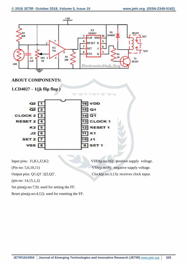
CIRCUIT PRINCIPLE:
The main principle of this Wireless Switch Circuit is in the functioning of LDR, LM741 Op-Amp and a
CD4027 JK Flip-Flop IC. In this circuit, all you need is to pass your hand above a simple Light Sensor, the
infamous LDR.The LDR is configured in such a way that, light from an LED will continuously fall on the
LDR and when you place your hand over (or pass your hand between the LED and LDR), the device
connected to the circuit will turn ON. This change is detected by an Op-Amp (LM741 is used here) and
triggers a flip-flop (CD4027 is used). The device will stay turned ON until you pass your hand over the
LDR again. The circuit shown is triggered on the leading edge of the switch pulse which means that output
changes when you again put your hand over LDR. From the circuit you can see that both J and K are tied to
high input so at every negative or positive transition, the clock pulse pin 13 toggles between high to low.
This can be verified with the help of the truth table of the JK flip flop. Therefore, when it receives the clock
pulse from IC1 due to hand over LDR, transistor connected to pin15 starts conducting and we will receive
the output with the help of relay. You can adjust the sensitivity of LDR with the help of VR1.
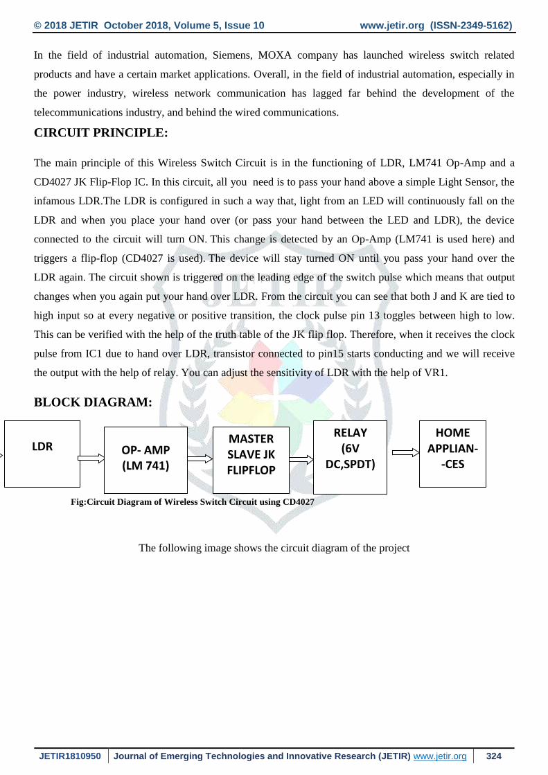
BLOCK DIAGRAM:
Fig:Circuit Diagram of Wireless Switch Circuit using CD4027
The following image shows the circuit diagram of the project
LDR
OP- AMP (LM 741)
MASTER SLAVE JK FLIPFLOP
RELAY (6V
DC,SPDT)
HOME APPLIAN-
-CES
© 2018 JETIR October 2018, Volume 5, Issue 10 www.jetir.org (ISSN-2349-5162)
JETIR1810950 Journal of Emerging Technologies and Innovative Research (JETIR) www.jetir.org 325
ABOUT COMPONENTS:
1.CD4027 – 1(jk flip flop )
Input pins: J1,K1,J2,K2. VDD(p.no:16): positive supply voltage.
(Pin no: 5,6,10,11) VSS(p.no:8): negative supply voltage.
Output pins: Q1,Q1’,Q2,Q2’. Clock(p.no:3,13): receives clock input.
(pin no: 14,15,1,2)
Set pins(p.no:7,9): used for setting the FF.
Reset pins(p.no:4,12): used for resetting the FF.

© 2018 JETIR October 2018, Volume 5, Issue 10 www.jetir.org (ISSN-2349-5162)
JETIR1810950 Journal of Emerging Technologies and Innovative Research (JETIR) www.jetir.org 326
Table1:JK-FLIPFLOP TRUTH TABLE
2. LM741 – 1:
The IC 741 operational amplifier looks like a small chip. The representation of 741 IC op-amp is given
below that comprises of eight pins. The most significant pins are 2,3 and 6, where pin2 and 3 are pin 2
and 3 denote inverting & non-inverting terminals and pin6 denotes output voltage. The triangular form in
the IC signifies an op-amp integrated circuit.The current version of the chip is denoted by the famous IC
741 op amp. The main function of this IC 741 is to do mathematical operations in various circuits. IC 741
op amp is made from various stages of transistor which commonly have three stages like differential i/p,
a push-pull o/p and an intermediate gain stage. The differential op-amps comprises of a set of FETs or
BJTs.
IC 741 OP-AMP:
Fig:2

© 2018 JETIR October 2018, Volume 5, Issue 10 www.jetir.org (ISSN-2349-5162)
JETIR1810950 Journal of Emerging Technologies and Innovative Research (JETIR) www.jetir.org 327
Pin-1 is Offset null.
Pin-2 is Inverting (-) i/p terminal.
Pin-3 is a non-inverting (+) i/p terminal.
Pin-4 is -Ve voltage supply (VCC)
Pin-5 is offset null.
Pin-6 is the o/p voltage.
Pin-7 is +ve voltage supply (+VCC)
Pin-8 is not connected.
3. RESISTORS:
10KΩ – 3 ,33KΩ – 1,1KΩ – 1
4. LDR:
An LDR is a component that has a (variable) resistance that changes with the light intensity that falls upon
it. This allows them to be used in light sensing circuits.
Fig: LDR Fig: LDR Circuit Symbol
Variation in resistance with changing light intensity
Fig: Intensity graph
The most common type of LDR has a resistance that falls with an increase in the light intensity falling upon
the device (as shown in the image above). The resistance of an LDR may typically have the following
resistances:
© 2018 JETIR October 2018, Volume 5, Issue 10 www.jetir.org (ISSN-2349-5162)
JETIR1810950 Journal of Emerging Technologies and Innovative Research (JETIR) www.jetir.org 328
5. LED:
In the simplest terms, a light-emitting diode (LED) is a semiconductor device that emits light when an
electric current is passed through it. Light is produced when the particles that carry the current (known as
electrons and holes) combine together within the semiconductor material.
The photon energy determines the wavelength of the emitted light, and hence its color. Different
semiconductor materials with different bandgaps produce different colors of light. The precise wavelength
(color) can be tuned by altering the composition of the light-emitting, or active, region.
CIRCUIT DESIGN:
The design of the circuit is very simple. First, connect a voltage divider (using either two resistors or a
potentiometer) to the Inverting terminal (Pin 2) of the Op-Amp LM741. Now, Connect the combination of
LDR and a resistor (which again form a voltage divider) to the Non-Inverting terminal (Pin 3) of the Op-
Amp. Place an independent LED (with current limiting resistor) in from of the LDR so that the light from
LED will always fall on the LDR.
Connect the output (Pin 6) of the Op-Amp to the clock (Pin 13) of the Flip-Flop IC CD4027. The output of
the Flip-Flop (Pin 15) is connected to the Relay Input of the 5V Relay Module.
Finally, connect the J (Pin 10) and K (Pin 11) Pins of CD4027 to +5V and Set (Pin 9) and Reset (Pin 12) to
GND. Rest of the connections with respect to power supply are self explanatory. In place of two fixed
resistors that are connected to the Inverting Input of the Op-Amp, you can connect a Potentiometer and vary
the sensitivity of the circuit.
© 2018 JETIR October 2018, Volume 5, Issue 10 www.jetir.org (ISSN-2349-5162)
JETIR1810950 Journal of Emerging Technologies and Innovative Research (JETIR) www.jetir.org 329
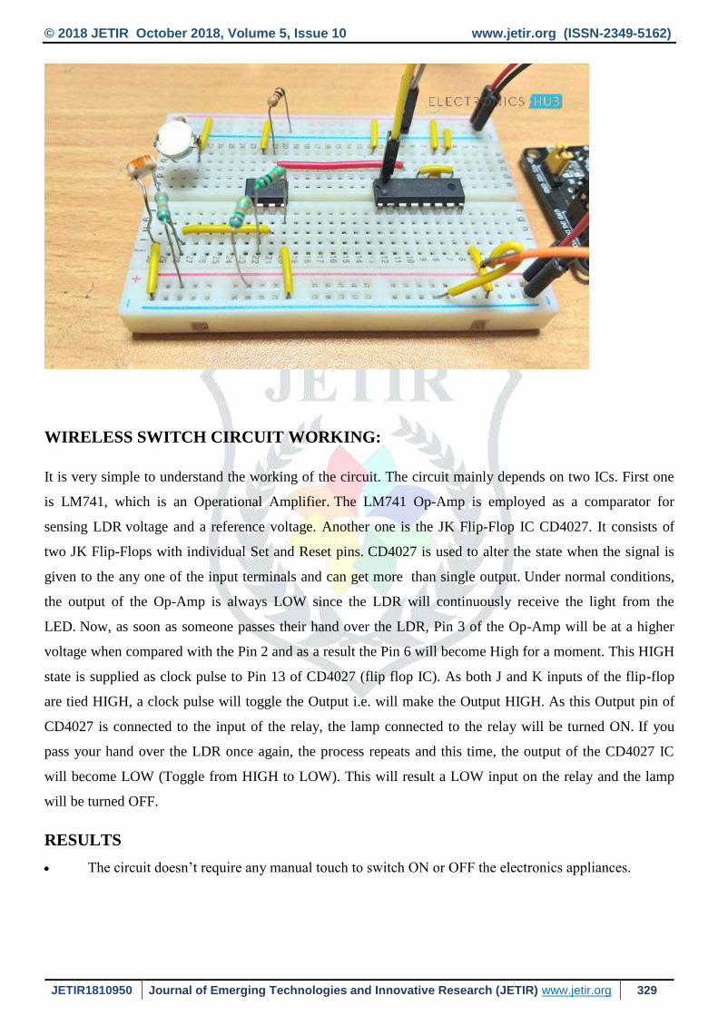
WIRELESS SWITCH CIRCUIT WORKING:
It is very simple to understand the working of the circuit. The circuit mainly depends on two ICs. First one
is LM741, which is an Operational Amplifier. The LM741 Op-Amp is employed as a comparator for
sensing LDR voltage and a reference voltage. Another one is the JK Flip-Flop IC CD4027. It consists of
two JK Flip-Flops with individual Set and Reset pins. CD4027 is used to alter the state when the signal is
given to the any one of the input terminals and can get more than single output. Under normal conditions,
the output of the Op-Amp is always LOW since the LDR will continuously receive the light from the
LED. Now, as soon as someone passes their hand over the LDR, Pin 3 of the Op-Amp will be at a higher
voltage when compared with the Pin 2 and as a result the Pin 6 will become High for a moment. This HIGH
state is supplied as clock pulse to Pin 13 of CD4027 (flip flop IC). As both J and K inputs of the flip-flop
are tied HIGH, a clock pulse will toggle the Output i.e. will make the Output HIGH. As this Output pin of
CD4027 is connected to the input of the relay, the lamp connected to the relay will be turned ON. If you
pass your hand over the LDR once again, the process repeats and this time, the output of the CD4027 IC
will become LOW (Toggle from HIGH to LOW). This will result a LOW input on the relay and the lamp
will be turned OFF.
RESULTS
The circuit doesn’t require any manual touch to switch ON or OFF the electronics appliances.

© 2018 JETIR October 2018, Volume 5, Issue 10 www.jetir.org (ISSN-2349-5162)
JETIR1810950 Journal of Emerging Technologies and Innovative Research (JETIR) www.jetir.org 330
CONCLUSIONS:
In this circuit the delay time between input and output is very less to produce an output for an applied
input.The power wastage in the circuit is very less because of low current sinking property of the op-amp
because of its high input impedance.The circuit doesn’t require any manual touch to switch ON or OFF the
electronics appliances.Because of the non-ideal behavior of op-amp and flip-flop the circuit output may
deviate from the ideal value.
REFERENCES:
J.B. Gupta, electronic devices and circuits, Kataria publications.
T Ahonen, R Virrankoski and M Elmusrati, Greenhouse Monitoring with Wireless Sensor Network,
University of Vaasa, Finland, Web. http://lipas.uwasa.fi/~rvir/greenhouse_mesa08.pdf, 2009.
Wireless Remote Switching System for Controlling Devices
Weiping Liu, Yanwen Liu, Ru Li, Pai Wang
D. Roy Chaudhary Linear integrated circuits, New age techno press.
.Anand Kumar, Fundamental of digital circuits, PHI learning private limited.
www.electronicsoru.com/mini project
www.electronicshub.com/mini project
www.wikipedia.com.