wm8960 ds datasheet - 1098183 - 1 - 4.2 - 1 · w pd, august 2013, rev 4.2 2 table of contents ......
TRANSCRIPT

w WM8960
Stereo CODEC with 1W Stereo Class D Speaker Drivers and Headphone Drivers for Portable Audio Applications
WOLFSON MICROELECTRONICS plc
Production Data, August 2013, Rev 4.2
Copyright 2013 Wolfson Microelectronics plc
CONTROLINTERFACE
SD
IN
SC
LK
MICBIAS
DCVDD DBVDDDGND
DAC-73 to 6dB1dB steps, mute
HP_L
HP_R
ADCREF, DACREF
AV
DD
AG
ND
VM
ID
50K50K
DAC
DIGITAL AUDIOINTERFACE
A-law and u-law support
AD
CD
AT
AD
CLR
C/G
PIO
1
BC
LK
MC
LK
DA
CD
AT
DA
CL
RC
ADC
ADC
PLL
LINPUT2
LINPUT1
LEFT MIXER
RIGHT MIXER
RINPUT1
ADCDIGITAL FILTERS
ALC
VOLUME
-17.25 to +30dB,0.75dB steps
INPUT PGAs OUT3
LINPUT3/JD2
RINPUT3/JD3
0, 13, 20, 29dB, mute
+
-vmid +
-12 -> 6dB,3dB steps,mute
-17.25 to +30dB,0.75dB steps
0, 13, 20, 29dB, mute
+
-vmid +-12 -> 6dB,3dB steps,mute
RINPUT2
SPK_LP
SPK_LN
SPK_RP
SPK_RN
SPKGND1
SPKVDD1
MONO MIXER
0 to -21dB, 3dB steps
0 to -21dB, 3dB steps
0 to -21dB, 3dB steps
0 to -21dB, 3dB steps
-73 to 6dB1dB steps, mute
0dB / -6dB
-73 to 6dB1dB steps, mute+BOOST
CLASS D
CLASS D
-73 to 6dB1dB steps, mute+BOOST
DACDIGITAL FILTERS
DE-EMPHASIS
3D ENHANCE
VOLUME
-12 -> 6dB,3dB steps,mute
-12 -> 6dB,3dB steps,mute
Jack Detect
Jack Detect
GPIO1
SPKGND2
SPKVDD2W
WM8960
DESCRIPTION
The WM8960 is a low power, high quality stereo CODEC designed for portable digital audio applications.
Stereo class D speaker drivers provide 1W per channel into 8 loads with a 5V supply. Low leakage, excellent PSRR and pop/click suppression mechanisms also allow direct battery connection to the speaker supply. Flexible speaker boost settings allow speaker output power to be maximised while minimising other analogue supply currents.
A highly flexible input configuration for up to three stereo sources is integrated, with a complete microphone interface. External component requirements are drastically reduced as no separate microphone, speaker or headphone amplifiers are required. Advanced on-chip digital signal processing performs automatic level control for the microphone or line input.
Stereo 24-bit sigma-delta ADCs and DACs are used with low power over-sampling digital interpolation and decimation filters and a flexible digital audio interface.
The master clock can be input directly or generated internally by an onboard PLL, supporting most commonly-used clocking schemes.
The WM8960 operates at analogue supply voltages down to 2.7V, although the digital supplies can operate at voltages down to 1.71V to save power. The speaker supply can operate at up to 5.5V, providing 1W per channel into 8 loads. Unused functions can be disabled using software control to save power.
The WM8960 is supplied in a very small and thin 5x5mm QFN package, ideal for use in hand-held and portable systems.
FEATURES DAC SNR 98dB (‘A’ weighted), THD -84dB at 48kHz, 3.3V ADC SNR 94dB (‘A’ weighted), THD -82dB at 48kHz, 3.3V Pop and click suppression 3D Enhancement Stereo Class D Speaker Driver
- <0.1% THD with 1W per channel into 8 BTL speakers - 70dB PSRR @217Hz - 87% efficiency (1W output) - Flexible internal switching clock
On-chip Headphone Driver - 40mW output power into 16 at 3.3V - Capless mode support - THD -75dB at 20mW, SNR 90dB with 16 load
Microphone Interface - Pseudo differential for high noise immunity - Integrated low noise MICBIAS - Programmable ALC / Limiter and Noise Gate
Low Power Consumption Low Supply Voltages
- Analogue 2.7V to 3.6V (Speaker supply up to 5.5V) - Digital core and I/O: 1.71V to 3.6V
On-chip PLL provides flexible clocking scheme Sample rates: 8, 11.025, 12, 16, 22.05, 24, 32, 44.1, 48 5x5x0.9mm QFN package
APPLICATIONS Games consoles Portable media / DVD players Mobile multimedia
WM8960 Production Data
w PD, August 2013, Rev 4.2
2
TABLE OF CONTENTS
DESCRIPTION ....................................................................................................... 1 FEATURES ............................................................................................................ 1 APPLICATIONS ..................................................................................................... 1 TABLE OF CONTENTS ......................................................................................... 2 PIN CONFIGURATION .......................................................................................... 3 ORDERING INFORMATION .................................................................................. 3 PIN DESCRIPTION ................................................................................................ 4 ABSOLUTE MAXIMUM RATINGS ........................................................................ 5 RECOMMENDED OPERATING CONDITIONS ..................................................... 5 ELECTRICAL CHARACTERISTICS ..................................................................... 6 OUTPUT PGA GAIN ............................................................................................ 10 TYPICAL POWER CONSUMPTION .................................................................... 11 SIGNAL TIMING REQUIREMENTS .................................................................... 13
SYSTEM CLOCK TIMING .............................................................................................. 13 AUDIO INTERFACE TIMING – MASTER MODE .......................................................... 13 AUDIO INTERFACE TIMING – SLAVE MODE .............................................................. 14 CONTROL INTERFACE TIMING – 2-WIRE MODE ....................................................... 15
INTERNAL POWER ON RESET CIRCUIT .......................................................... 16 DEVICE DESCRIPTION ...................................................................................... 18
INTRODUCTION ............................................................................................................ 18 INPUT SIGNAL PATH .................................................................................................... 19 ANALOGUE TO DIGITAL CONVERTER (ADC) ............................................................ 26 AUTOMATIC LEVEL CONTROL (ALC) ......................................................................... 28 OUTPUT SIGNAL PATH ................................................................................................ 31 ANALOGUE OUTPUTS ................................................................................................. 37 ENABLING THE OUTPUTS ........................................................................................... 41 HEADPHONE OUTPUT ................................................................................................. 41 CLASS D SPEAKER OUTPUTS .................................................................................... 42 VOLUME UPDATES ...................................................................................................... 43 HEADPHONE JACK DETECT ....................................................................................... 45 THERMAL SHUTDOWN ................................................................................................ 46 GENERAL PURPOSE INPUT/OUTPUT ........................................................................ 47 DIGITAL AUDIO INTERFACE ........................................................................................ 48 AUDIO INTERFACE CONTROL .................................................................................... 52 CLOCKING AND SAMPLE RATES ................................................................................ 56 CONTROL INTERFACE................................................................................................. 63 POWER MANAGEMENT ............................................................................................... 63
REGISTER MAP .................................................................................................. 67 REGISTER BITS BY ADDRESS .................................................................................... 68
DIGITAL FILTER CHARACTERISTICS .............................................................. 82 ADC FILTER RESPONSES ........................................................................................... 83 DAC FILTER RESPONSES ........................................................................................... 83 DE-EMPHASIS FILTER RESPONSES .......................................................................... 85
APPLICATIONS INFORMATION ........................................................................ 86 RECOMMENDED EXTERNAL COMPONENTS ............................................................ 86
IMPORTANT NOTICE ......................................................................................... 90 ADDRESS: ..................................................................................................................... 90
REVISION HISTORY ........................................................................................... 91
Production Data WM8960
w PD, August 2013, Rev 4.2
3
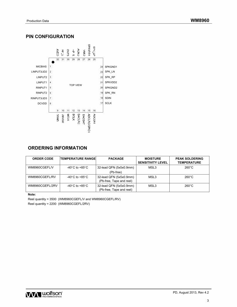
PIN CONFIGURATION
1
2
3
4
5
6
7
8
24
23
22
21
20
19
18
17
161514131211109
2526272829303132
TOP VIEW
RINPUT2
RINPUT1
LINPUT3/JD2
LINPUT1
LINPUT2
RINPUT3/JD3 SDIN
SPKVDD2
SPK_RN
SPKGND2
SPK_RP
SPK_LN
SCLKDCVDD
SPKGND1MICBIAS
ORDERING INFORMATION
ORDER CODE TEMPERATURE RANGE PACKAGE MOISTURE SENSITIVITY LEVEL
PEAK SOLDERING TEMPERATURE
WM8960CGEFL/V -40C to +85C 32-lead QFN (5x5x0.9mm)
(Pb-free)
MSL3 260°C
WM8960CGEFL/RV -40C to +85C 32-lead QFN (5x5x0.9mm)(Pb-free, Tape and reel)
MSL3 260°C
WM8960CGEFL/2RV -40C to +85C 32-lead QFN (5x5x0.9mm)(Pb-free, Tape and reel)
MSL3 260°C
Note:
Reel quantity = 3500 (WM8960CGEFL/V and WM8960CGEFL/RV)
Reel quantity = 2200 (WM8960CGEFL/2RV)

WM8960 Production Data
w PD, August 2013, Rev 4.2
4
PIN DESCRIPTION
PIN NO NAME TYPE DESCRIPTION
1 MICBIAS Analogue Output Microphone bias
2 LINPUT3 / JD2 Analogue Input Left channel line input /
Left channel positive differential MIC input /
Jack detect input pin
3 LINPUT2 Analogue Input Left channel line input /
Left channel positive differential MIC input
4 LINPUT1 Analogue Input Left channel single-ended MIC input /
Left channel negative differential MIC input
5 RINPUT1 Analogue Input Right channel single-ended MIC input /
Right channel negative differential MIC input
6 RINPUT2 Analogue Input Right channel line input /
Right channel positive differential MIC input
7 RINPUT3 / JD3 Analogue Input Right channel line input /
Right channel positive differential MIC input /
Jack detect input pin
8 DCVDD Supply Digital core supply
9 DGND Supply Digital ground (Return path for both DCVDD and DBVDD)
10 DBVDD Supply Digital buffer (I/O) supply
11 MCLK Digital Input Master clock
12 BCLK Digital Input / Output Audio interface bit clock
13 DACLRC Digital Input / Output Audio interface DAC left / right clock
14 DACDAT Digital Input DAC digital audio data
15 ADCLRC / GPIO1 Digital Input / Output Audio interface ADC left / right clock / GPIO1 pin
16 ADCDAT Digital Output ADC digital audio data
17 SCLK Digital Input Control interface clock input
18 SDIN Digital Input/Output Control interface data input / 2-wire acknowledge output
19 SPK_RN Analogue Output Right speaker negative output
20 SPKGND2 Supply Ground for speaker drivers 2
21 SPKVDD2 Supply Supply for speaker drivers 2
22 SPK_RP Analogue Output Right speaker positive output
23 SPK_LN Analogue Output Left speaker negative output
24 SPKGND1 Supply Ground for speaker drivers 1
25 SPK_LP Analogue Output Left speaker positive output
26 SPKVDD1 Supply Supply for speaker drivers 1
27 VMID Analogue Output Midrail voltage decoupling capacitor
28 AGND Supply Analogue ground (Return path for AVDD)
29 HP_R Analogue Output Right output (Line or headphone)
30 OUT3 Analogue Output Mono, left, right or buffered midrail output for capless mode
31 HP_L Analogue Output Left output (Line or headphone)
32 AVDD Supply Analogue supply
33 GND_PADDLE Die Paddle (Note 1)
Note:
1. It is recommended that the QFN ground paddle should be connected to analogue ground on the application PCB.
Production Data WM8960
w PD, August 2013, Rev 4.2
5
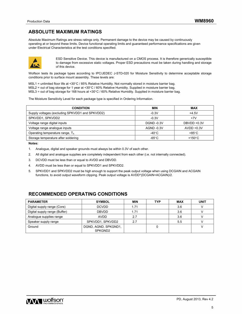
ABSOLUTE MAXIMUM RATINGS
Absolute Maximum Ratings are stress ratings only. Permanent damage to the device may be caused by continuously operating at or beyond these limits. Device functional operating limits and guaranteed performance specifications are given under Electrical Characteristics at the test conditions specified.
ESD Sensitive Device. This device is manufactured on a CMOS process. It is therefore generically susceptible to damage from excessive static voltages. Proper ESD precautions must be taken during handling and storage of this device.
Wolfson tests its package types according to IPC/JEDEC J-STD-020 for Moisture Sensitivity to determine acceptable storage conditions prior to surface mount assembly. These levels are:
MSL1 = unlimited floor life at <30C / 85% Relative Humidity. Not normally stored in moisture barrier bag. MSL2 = out of bag storage for 1 year at <30C / 60% Relative Humidity. Supplied in moisture barrier bag. MSL3 = out of bag storage for 168 hours at <30C / 60% Relative Humidity. Supplied in moisture barrier bag.
The Moisture Sensitivity Level for each package type is specified in Ordering Information.
CONDITION MIN MAX
Supply voltages (excluding SPKVDD1 and SPKVDD2) -0.3V +4.5V
SPKVDD1, SPKVDD2 -0.3V +7V
Voltage range digital inputs DGND -0.3V DBVDD +0.3V
Voltage range analogue inputs AGND -0.3V AVDD +0.3V
Operating temperature range, TA -40C +85C
Storage temperature after soldering -65C +150C
Notes:
1. Analogue, digital and speaker grounds must always be within 0.3V of each other.
2. All digital and analogue supplies are completely independent from each other (i.e. not internally connected).
3. DCVDD must be less than or equal to AVDD and DBVDD.
4. AVDD must be less than or equal to SPKVDD1 and SPKVDD2.
5. SPKVDD1 and SPKVDD2 must be high enough to support the peak output voltage when using DCGAIN and ACGAIN functions, to avoid output waveform clipping. Peak output voltage is AVDD*(DCGAIN+ACGAIN)/2.
RECOMMENDED OPERATING CONDITIONS
PARAMETER SYMBOL MIN TYP MAX UNIT
Digital supply range (Core) DCVDD 1.71 3.6 V
Digital supply range (Buffer) DBVDD 1.71 3.6 V
Analogue supplies range AVDD 2.7 3.6 V
Speaker supply range SPKVDD1, SPKVDD2 2.7 5.5 V
Ground DGND, AGND, SPKGND1, SPKGND2
0 V
WM8960 Production Data
w PD, August 2013, Rev 4.2
6
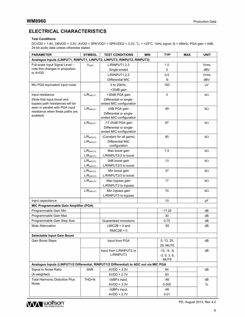
ELECTRICAL CHARACTERISTICS
Test Conditions
DCVDD = 1.8V, DBVDD = 3.3V, AVDD = SPKVDD1 = SPKVDD2 = 3.3V, TA = +25oC, 1kHz signal, fs = 48kHz, PGA gain = 0dB, 24-bit audio data unless otherwise stated.
PARAMETER SYMBOL TEST CONDITIONS MIN TYP MAX UNIT
Analogue Inputs (LINPUT1, RINPUT1, LINPUT2, LINPUT3, RINPUT2, RINPUT3)
Full-scale Input Signal Level – note this changes in proportion to AVDD
VINFS L/RINPUT1,2,3
Single-ended
1.0
0
Vrms
dBV
L/RINPUT1,2,3
Differential MIC
0.5
-6
Vrms
dBV
Mic PGA equivalent input noise 0 to 20kHz,
+30dB gain
150 uV
Input resistance
(Note that input boost and bypass path resistances will be seen in parallel with PGA input resistance when these paths are enabled)
L/RINPUT1 +30dB PGA gain
Differential or single-ended MIC configuration
3 k
L/RINPUT1 0dB PGA gain
Differential or single-ended MIC configuration
49
k
L/RINPUT1 -17.25dB PGA gain
Differential or single-ended MIC configuration
87
k
L/RINPUT2,
L/RINPUT3
(Constant for all gains)
Differential MIC configuration
85 k
L/RINPUT2,
L/RINPUT3
Max boost gain
L/RINPUT2/3 to boost
7.5 k
L/RINPUT2,
L/RINPUT3
0dB boost gain
L/RINPUT2/3 to boost
13 k
L/RINPUT2,
L/RINPUT3
Min boost gain
L/RINPUT2/3 to boost
37
k
L/RINPUT3 Max bypass gain
L/RINPUT3 to bypass
17 k
L/RINPUT3 Min bypass gain
L/RINPUT3 to bypass
70
k
Input capacitance 10 pF
MIC Programmable Gain Amplifier (PGA)
Programmable Gain Min -17.25 dB
Programmable Gain Max 30 dB
Programmable Gain Step Size Guaranteed monotonic 0.75 dB
Mute Attenuation LMIC2B = 0 and
RMIC2B = 0
85 dB
Selectable Input Gain Boost
Gain Boost Steps Input from PGA 0, 13, 20,
29, MUTE
dB
Input from L/RINPUT2 or L/RINPUT3
-12, -9, -6,
-3, 0, 3, 6, MUTE
dB
Analogue Inputs (LINPUT1/2 Differential, RINPUT1/2 Differential) to ADC out via MIC PGA
Signal to Noise Ratio
(A-weighted)
SNR AVDD = 3.3V 94 dB
AVDD = 2.7V 93
Total Harmonic Distortion Plus Noise
THD+N -3dBFs input,
AVDD = 3.3V
-86
0.005
dB
%
-3dBFs input,
AVDD = 2.7V
-80
0.01
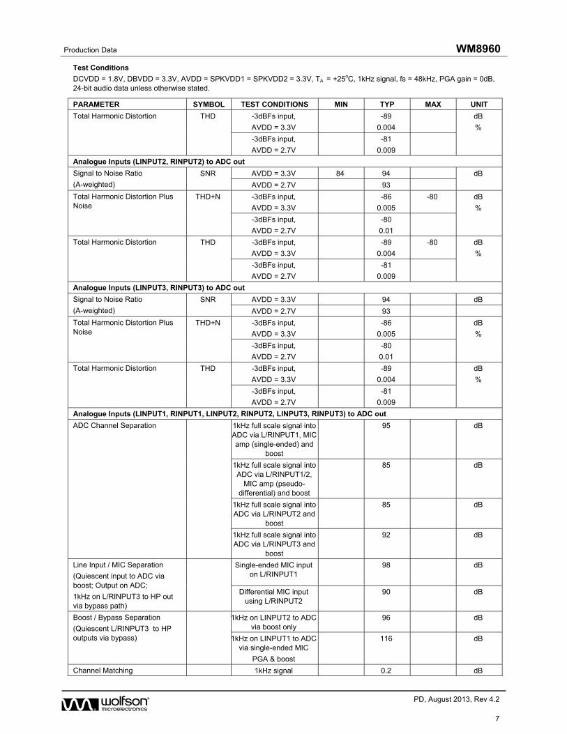
Production Data WM8960
w PD, August 2013, Rev 4.2
7
Test Conditions
DCVDD = 1.8V, DBVDD = 3.3V, AVDD = SPKVDD1 = SPKVDD2 = 3.3V, TA = +25oC, 1kHz signal, fs = 48kHz, PGA gain = 0dB, 24-bit audio data unless otherwise stated.
PARAMETER SYMBOL TEST CONDITIONS MIN TYP MAX UNIT
Total Harmonic Distortion THD -3dBFs input,
AVDD = 3.3V
-89
0.004
dB
%
-3dBFs input,
AVDD = 2.7V
-81
0.009
Analogue Inputs (LINPUT2, RINPUT2) to ADC out
Signal to Noise Ratio
(A-weighted)
SNR AVDD = 3.3V 84 94 dB
AVDD = 2.7V 93
Total Harmonic Distortion Plus Noise
THD+N -3dBFs input,
AVDD = 3.3V
-86
0.005
-80 dB
%
-3dBFs input,
AVDD = 2.7V
-80
0.01
Total Harmonic Distortion THD -3dBFs input,
AVDD = 3.3V
-89
0.004
-80 dB
%
-3dBFs input,
AVDD = 2.7V
-81
0.009
Analogue Inputs (LINPUT3, RINPUT3) to ADC out
Signal to Noise Ratio
(A-weighted)
SNR AVDD = 3.3V 94 dB
AVDD = 2.7V 93
Total Harmonic Distortion Plus Noise
THD+N -3dBFs input,
AVDD = 3.3V
-86
0.005
dB
%
-3dBFs input,
AVDD = 2.7V
-80
0.01
Total Harmonic Distortion THD -3dBFs input,
AVDD = 3.3V
-89
0.004
dB
%
-3dBFs input,
AVDD = 2.7V
-81
0.009
Analogue Inputs (LINPUT1, RINPUT1, LINPUT2, RINPUT2, LINPUT3, RINPUT3) to ADC out
ADC Channel Separation 1kHz full scale signal into ADC via L/RINPUT1, MIC amp (single-ended) and
boost
95 dB
1kHz full scale signal into ADC via L/RINPUT1/2,
MIC amp (pseudo-differential) and boost
85 dB
1kHz full scale signal into ADC via L/RINPUT2 and
boost
85 dB
1kHz full scale signal into ADC via L/RINPUT3 and
boost
92 dB
Line Input / MIC Separation
(Quiescent input to ADC via boost; Output on ADC;
1kHz on L/RINPUT3 to HP out via bypass path)
Single-ended MIC input on L/RINPUT1
98 dB
Differential MIC input using L/RINPUT2
90 dB
Boost / Bypass Separation
(Quiescent L/RINPUT3 to HP outputs via bypass)
1kHz on LINPUT2 to ADC via boost only
96 dB
1kHz on LINPUT1 to ADC via single-ended MIC
PGA & boost
116 dB
Channel Matching 1kHz signal 0.2 dB
WM8960 Production Data
w PD, August 2013, Rev 4.2
8
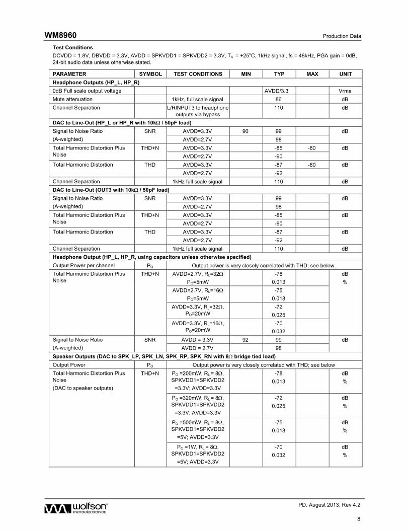
Test Conditions
DCVDD = 1.8V, DBVDD = 3.3V, AVDD = SPKVDD1 = SPKVDD2 = 3.3V, TA = +25oC, 1kHz signal, fs = 48kHz, PGA gain = 0dB, 24-bit audio data unless otherwise stated.
PARAMETER SYMBOL TEST CONDITIONS MIN TYP MAX UNIT
Headphone Outputs (HP_L, HP_R)
0dB Full scale output voltage AVDD/3.3 Vrms
Mute attenuation 1kHz, full scale signal 86 dB
Channel Separation L/RINPUT3 to headphone outputs via bypass
110 dB
DAC to Line-Out (HP_L or HP_R with 10k / 50pF load)
Signal to Noise Ratio
(A-weighted)
SNR AVDD=3.3V 90 99 dB
AVDD=2.7V 98
Total Harmonic Distortion Plus Noise
THD+N AVDD=3.3V -85 -80 dB
AVDD=2.7V -90
Total Harmonic Distortion THD AVDD=3.3V -87 -80 dB
AVDD=2.7V -92
Channel Separation 1kHz full scale signal 110 dB
DAC to Line-Out (OUT3 with 10k / 50pF load)
Signal to Noise Ratio
(A-weighted)
SNR AVDD=3.3V 99 dB
AVDD=2.7V 98
Total Harmonic Distortion Plus Noise
THD+N AVDD=3.3V -85 dB
AVDD=2.7V -90
Total Harmonic Distortion THD AVDD=3.3V -87 dB
AVDD=2.7V -92
Channel Separation 1kHz full scale signal 110 dB
Headphone Output (HP_L, HP_R, using capacitors unless otherwise specified)
Output Power per channel PO Output power is very closely correlated with THD; see below.
Total Harmonic Distortion Plus Noise
THD+N AVDD=2.7V, RL=32
PO=5mW
-78
0.013
dB
%
AVDD=2.7V, RL=16
PO=5mW
-75
0.018
AVDD=3.3V, RL=32, PO=20mW
-72
0.025
AVDD=3.3V, RL=16, PO=20mW
-70
0.032
Signal to Noise Ratio
(A-weighted)
SNR AVDD = 3.3V 92 99 dB
AVDD = 2.7V 98
Speaker Outputs (DAC to SPK_LP, SPK_LN, SPK_RP, SPK_RN with 8 bridge tied load)
Output Power PO Output power is very closely correlated with THD; see below
Total Harmonic Distortion Plus Noise
(DAC to speaker outputs)
THD+N PO =200mW, RL = 8, SPKVDD1=SPKVDD2
=3.3V; AVDD=3.3V
-78
0.013
dB
%
PO =320mW, RL = 8, SPKVDD1=SPKVDD2
=3.3V; AVDD=3.3V
-72
0.025
dB
%
PO =500mW, RL = 8, SPKVDD1=SPKVDD2
=5V; AVDD=3.3V
-75
0.018
dB
%
PO =1W, RL = 8, SPKVDD1=SPKVDD2
=5V; AVDD=3.3V
-70
0.032
dB
%

Production Data WM8960
w PD, August 2013, Rev 4.2
9
Test Conditions
DCVDD = 1.8V, DBVDD = 3.3V, AVDD = SPKVDD1 = SPKVDD2 = 3.3V, TA = +25oC, 1kHz signal, fs = 48kHz, PGA gain = 0dB, 24-bit audio data unless otherwise stated.
PARAMETER SYMBOL TEST CONDITIONS MIN TYP MAX UNIT
Total Harmonic Distortion Plus Noise
(LINPUT3 and RINPUT3 to speaker outputs)
THD+N PO =200mW, RL = 8, SPKVDD1=SPKVDD2
=3.3V; AVDD=3.3V
-78
0.013
dB
%
PO =320mW, RL = 8, SPKVDD1=SPKVDD2
=3.3V; AVDD=3.3V
-72
0.025
dB
%
PO =500mW, RL = 8, SPKVDD1=SPKVDD2
=5V; AVDD=3.3V
-75
0.018
dB
%
PO =1W, RL = 8, SPKVDD1=SPKVDD2
=5V; AVDD=3.3V
-70
0.032
dB
%
Signal to Noise Ratio
(A-weighted)
(DAC to speaker outputs)
SNR SPKVDD1=SPKVDD2
=3.3V; AVDD=3.3V;
RL = 8, ref=2.0Vrms
90 dB
SPKVDD1=SPKVDD2
=5V; AVDD=3.3V;
RL = 8, ref=2.8Vrms
92 dB
Signal to Noise Ratio
(A-weighted)
(LINNPUT3 and RINPUT3 to speaker outputs)
SNR SPKVDD1=SPKVDD2
=3.3V; AVDD=3.3V;
RL = 8, ref=2.0Vrms
90 dB
SPKVDD1=SPKVDD2
=5V; AVDD=3.3V;
RL = 8, ref=2.8Vrms
92 dB
Speaker Supply Leakage current ISPKVDD SPKVDD1=SPKVDD2
=5V;
All other supplies disconnected
1 uA
SPKVDD1=SPKVDD2
=5V;
All other supplies 0V
1 uA
Power Supply Rejection Ratio (100mV ripple on SPKVDD1/SPKVDD2 @217Hz)
PSRR DAC to speaker playback 80 dB
L/RINPUT3 to speaker playback
80 dB
Analogue Reference Levels
Midrail Reference Voltage VMID –3% AVDD/2 +3% V
Microphone Bias
Bias Voltage VMICBIAS 3mA load current
MBSEL=1
–5% 0.9AVDD + 5% V
3mA load current
MBSEL=0
–5% 0.65AVDD + 5% V
Bias Current Source IMICBIAS 3 mA
Output Noise Voltage Vn 1K to 20kHz 15 nV/Hz
Digital Input / Output
Input HIGH Level VIH 0.7DBVDD V
Input LOW Level VIL 0.3DBVDD V
Output HIGH Level VOH IOL=1mA 0.9DBVDD V
Output LOW Level VOL IOH=-1mA 0.1DBVDD V
Input capacitance 10 pF
Input leakage -0.9 0.9 uA
WM8960 Production Data
w PD, August 2013, Rev 4.2
10
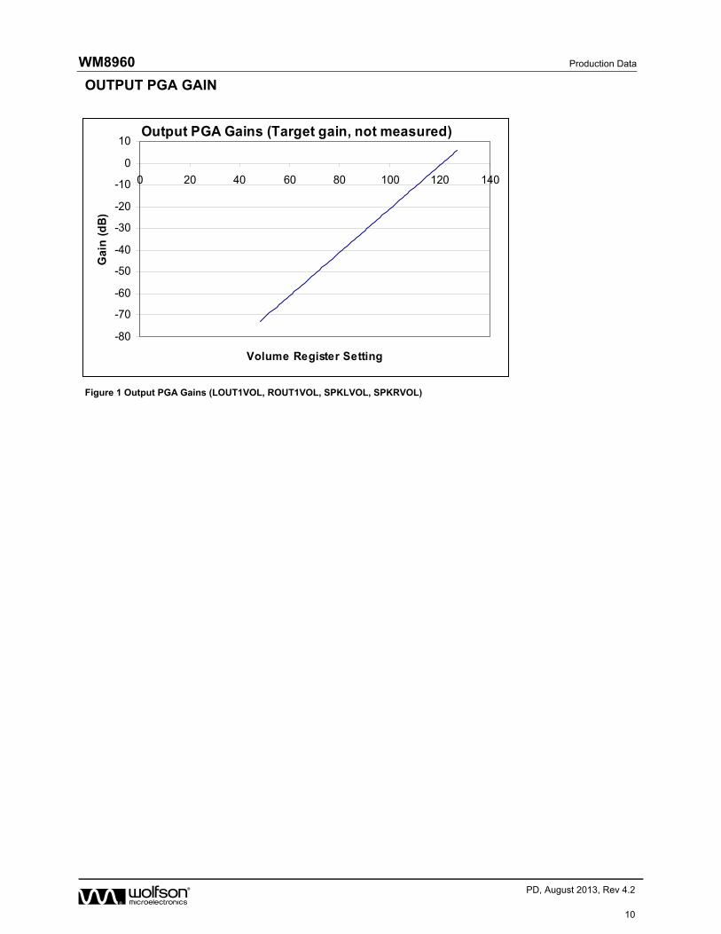
OUTPUT PGA GAIN
Output PGA Gains (Target gain, not measured)
-80
-70
-60
-50
-40
-30
-20
-10
0
10
0 20 40 60 80 100 120 140
Volume Register Setting
Gai
n (
dB
)
Figure 1 Output PGA Gains (LOUT1VOL, ROUT1VOL, SPKLVOL, SPKRVOL)
Production Data WM8960
w PD, August 2013, Rev 4.2
11
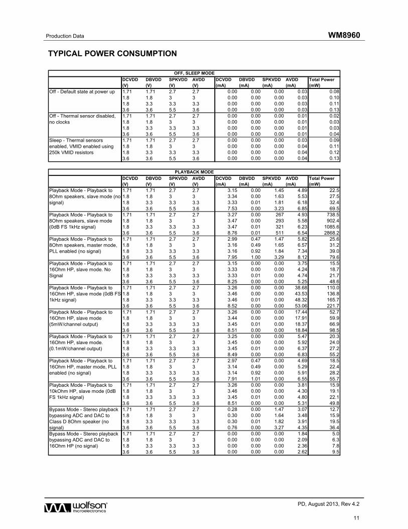
TYPICAL POWER CONSUMPTION
DCVDD (V)
DBVDD (V)
SPKVDD (V)
AVDD (V)
DCVDD (mA)
DBVDD (mA)
SPKVDD (mA)
AVDD (mA)
Total Power (mW)
1.71 1.71 2.7 2.7 0.00 0.00 0.00 0.03 0.081.8 1.8 3 3 0.00 0.00 0.00 0.03 0.101.8 3.3 3.3 3.3 0.00 0.00 0.00 0.03 0.113.6 3.6 5.5 3.6 0.00 0.00 0.00 0.03 0.131.71 1.71 2.7 2.7 0.00 0.00 0.00 0.01 0.021.8 1.8 3 3 0.00 0.00 0.00 0.01 0.031.8 3.3 3.3 3.3 0.00 0.00 0.00 0.01 0.033.6 3.6 5.5 3.6 0.00 0.00 0.00 0.01 0.041.71 1.71 2.7 2.7 0.00 0.00 0.00 0.03 0.091.8 1.8 3 3 0.00 0.00 0.00 0.04 0.111.8 3.3 3.3 3.3 0.00 0.00 0.00 0.04 0.123.6 3.6 5.5 3.6 0.00 0.00 0.00 0.04 0.13
OFF, SLEEP MODE
Sleep - Thermal sensors enabled, VMID enabled using 250k VMID resistors
Off - Thermal sensor disabled, no clocks
Off - Default state at power up
DCVDD (V)
DBVDD (V)
SPKVDD (V)
AVDD (V)
DCVDD (mA)
DBVDD (mA)
SPKVDD (mA)
AVDD (mA)
Total Power (mW)
1.71 1.71 2.7 2.7 3.15 0.00 1.45 4.89 22.51.8 1.8 3 3 3.34 0.00 1.63 5.53 27.51.8 3.3 3.3 3.3 3.33 0.01 1.81 6.18 32.43.6 3.6 5.5 3.6 7.53 0.00 3.23 6.85 69.51.71 1.71 2.7 2.7 3.27 0.00 267 4.93 738.51.8 1.8 3 3 3.47 0.00 293 5.58 902.41.8 3.3 3.3 3.3 3.47 0.01 321 6.23 1085.63.6 3.6 5.5 3.6 8.76 0.01 511 6.54 2868.21.71 1.71 2.7 2.7 2.99 0.47 1.47 5.82 25.61.8 1.8 3 3 3.16 0.49 1.65 6.57 31.21.8 3.3 3.3 3.3 3.16 0.92 1.84 7.34 39.03.6 3.6 5.5 3.6 7.95 1.00 3.29 8.12 79.61.71 1.71 2.7 2.7 3.15 0.00 0.00 3.75 15.51.8 1.8 3 3 3.33 0.00 0.00 4.24 18.71.8 3.3 3.3 3.3 3.33 0.01 0.00 4.74 21.73.6 3.6 5.5 3.6 8.25 0.00 0.00 5.25 48.61.71 1.71 2.7 2.7 3.26 0.00 0.00 38.68 110.01.8 1.8 3 3 3.46 0.00 0.00 43.53 136.81.8 3.3 3.3 3.3 3.46 0.01 0.00 48.32 165.73.6 3.6 5.5 3.6 8.52 0.00 0.00 53.06 221.71.71 1.71 2.7 2.7 3.26 0.00 0.00 17.44 52.71.8 1.8 3 3 3.44 0.00 0.00 17.91 59.91.8 3.3 3.3 3.3 3.45 0.01 0.00 18.37 66.93.6 3.6 5.5 3.6 8.51 0.00 0.00 18.84 98.51.71 1.71 2.7 2.7 3.25 0.00 0.00 5.47 20.31.8 1.8 3 3 3.45 0.00 0.00 5.92 24.01.8 3.3 3.3 3.3 3.45 0.01 0.00 6.37 27.23.6 3.6 5.5 3.6 8.49 0.00 0.00 6.83 55.21.71 1.71 2.7 2.7 2.97 0.47 0.00 4.69 18.51.8 1.8 3 3 3.14 0.49 0.00 5.29 22.41.8 3.3 3.3 3.3 3.14 0.92 0.00 5.91 28.23.6 3.6 5.5 3.6 7.91 1.01 0.00 6.55 55.71.71 1.71 2.7 2.7 3.26 0.00 0.00 3.81 15.91.8 1.8 3 3 3.46 0.00 0.00 4.30 19.11.8 3.3 3.3 3.3 3.45 0.01 0.00 4.80 22.13.6 3.6 5.5 3.6 8.51 0.00 0.00 5.31 49.81.71 1.71 2.7 2.7 0.28 0.00 1.47 3.07 12.71.8 1.8 3 3 0.30 0.00 1.64 3.48 15.91.8 3.3 3.3 3.3 0.30 0.01 1.82 3.91 19.53.6 3.6 5.5 3.6 0.76 0.00 3.27 4.35 36.41.71 1.71 2.7 2.7 0.00 0.00 0.00 1.84 5.01.8 1.8 3 3 0.00 0.00 0.00 2.09 6.31.8 3.3 3.3 3.3 0.00 0.00 0.00 2.36 7.83.6 3.6 5.5 3.6 0.00 0.00 0.00 2.62 9.5
Bypass Mode - Stereo playback bypassing ADC and DAC to 16Ohm HP (no signal)
Bypass Mode - Stereo playback bypassing ADC and DAC to Class D 8Ohm speaker (no signal)
Playback Mode - Playback to 10kOhm HP, slave mode (0dB FS 1kHz signal)
Playback Mode - Playback to 16Ohm HP, master mode, PLL enabled (no signal)
Playback Mode - Playback to 16Ohm HP, slave mode. (0.1mW/channel output)
Playback Mode - Playback to 16Ohm HP, slave mode (5mW/channel output)
Playback Mode - Playback to 8Ohm speakers, slave mode (no signal)
PLAYBACK MODE
Playback Mode - Playback to 8Ohm speakers, slave mode (0dB FS 1kHz signal)
Playback Mode - Playback to 8Ohm speakers, master mode, PLL enabled (no signal)
Playback Mode - Playback to 16Ohm HP, slave mode. No Signal
Playback Mode - Playback to 16Ohm HP, slave mode (0dB FS 1kHz signal)
WM8960 Production Data
w PD, August 2013, Rev 4.2
12
DCVDD (V)
DBVDD (V)
SPKVDD (V)
AVDD (V)
DCVDD (mA)
DBVDD (mA)
SPKVDD (mA)
AVDD (mA)
Total Power (mW)
1.71 1.71 2.7 2.7 1.10 0.01 0.00 5.84 17.71.8 1.8 3 3 1.17 0.01 0.00 6.24 20.81.8 3.3 3.3 3.3 1.17 0.01 0.00 6.64 24.13.6 3.6 5.5 3.6 2.92 0.01 0.00 7.05 35.91.71 1.71 2.7 2.7 2.99 0.01 0.00 5.99 21.31.8 1.8 3 3 3.19 0.01 0.00 6.41 25.01.8 3.3 3.3 3.3 3.19 0.03 0.00 6.83 28.43.6 3.6 5.5 3.6 7.94 0.02 0.00 7.26 54.81.71 1.71 2.7 2.7 3.27 0.02 0.00 6.01 21.91.8 1.8 3 3 3.47 0.02 0.00 6.44 25.61.8 3.3 3.3 3.3 3.47 0.03 0.00 6.86 29.03.6 3.6 5.5 3.6 8.63 0.03 0.00 7.29 57.41.71 1.71 2.7 2.7 3.01 0.01 0.00 5.99 21.41.8 1.8 3 3 3.20 0.02 0.00 6.41 25.01.8 3.3 3.3 3.3 3.20 0.03 0.00 6.84 28.43.6 3.6 5.5 3.6 7.97 0.03 0.00 7.27 54.9
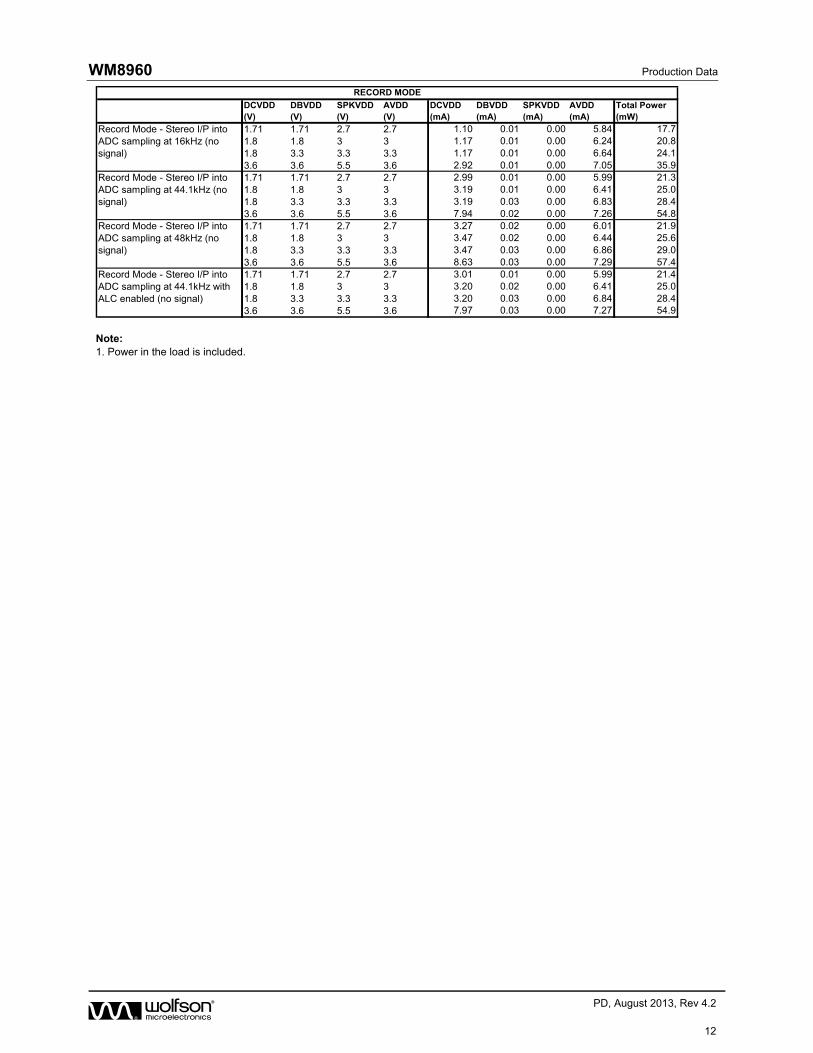
RECORD MODE
Record Mode - Stereo I/P into ADC sampling at 16kHz (no signal)
Record Mode - Stereo I/P into ADC sampling at 44.1kHz (no signal)
Record Mode - Stereo I/P into ADC sampling at 48kHz (no signal)
Record Mode - Stereo I/P into ADC sampling at 44.1kHz with ALC enabled (no signal)
Note: 1. Power in the load is included.
Production Data WM8960
w PD, August 2013, Rev 4.2
13
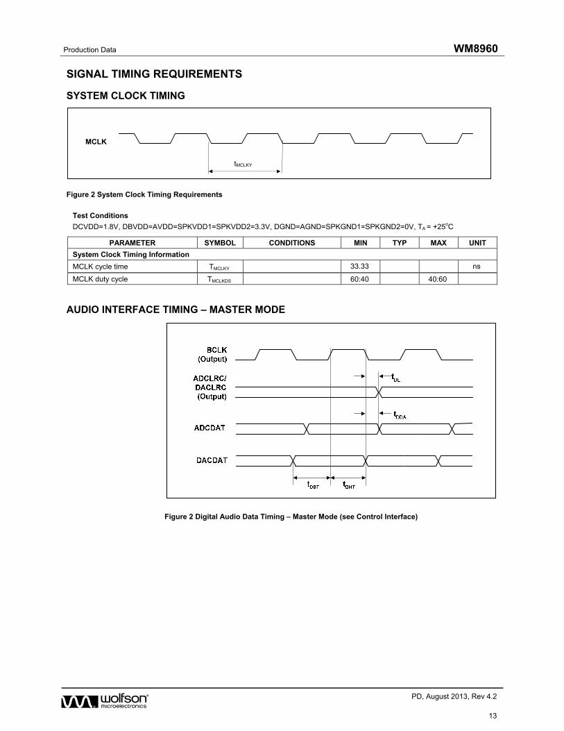
SIGNAL TIMING REQUIREMENTS
SYSTEM CLOCK TIMING
Figure 2 System Clock Timing Requirements
Test Conditions
DCVDD=1.8V, DBVDD=AVDD=SPKVDD1=SPKVDD2=3.3V, DGND=AGND=SPKGND1=SPKGND2=0V, TA = +25oC
PARAMETER SYMBOL CONDITIONS MIN TYP MAX UNIT
System Clock Timing Information
MCLK cycle time TMCLKY 33.33 ns
MCLK duty cycle TMCLKDS 60:40 40:60
AUDIO INTERFACE TIMING – MASTER MODE
Figure 2 Digital Audio Data Timing – Master Mode (see Control Interface)
MCLK
tMCLKY

WM8960 Production Data
w PD, August 2013, Rev 4.2
14
Test Conditions
DCVDD=1.8V, DBVDD=AVDD=SPKVDD1=SPKVDD2=3.3V, DGND=AGND=SPKGND1=SPKGND2=0V, TA=+25oC, Slave Mode, fs=48kHz, MCLK=256fs, 24-bit data, unless otherwise stated.
PARAMETER SYMBOL MIN TYP MAX UNIT
Audio Data Input Timing Information
ADCLRC/DACLRC propagation delay from BCLK falling edge tDL 10 ns
ADCDAT propagation delay from BCLK falling edge tDDA 10 ns
DACDAT setup time to BCLK rising edge tDST 10 ns
DACDAT hold time from BCLK rising edge tDHT 10 ns
AUDIO INTERFACE TIMING – SLAVE MODE
Figure 3 Digital Audio Data Timing – Slave Mode
Test Conditions
DCVDD=1.8V, DBVDD=AVDD=SPKVDD1=SPKVDD2=3.3V, DGND=AGND=SPKGND1=SPKGND2=0V, TA=+25oC, Slave Mode, fs=48kHz, MCLK= 256fs, 24-bit data, unless otherwise stated.
PARAMETER SYMBOL MIN TYP MAX UNIT
Audio Data Input Timing Information
BCLK cycle time tBCY 50 ns
BCLK pulse width high tBCH 20 ns
BCLK pulse width low tBCL 20 ns
ADCLRC/DACLRC set-up time to BCLK rising edge tLRSU 10 ns
ADCLRC/DACLRC hold time from BCLK rising edge tLRH 10 ns
DACDAT hold time from BCLK rising edge tDH 10 ns
ADCDAT propagation delay from BCLK falling edge tDD 10 ns
DACDAT set-up time to BCLK rising edge tDS 10 ns
Note:
BCLK period should always be greater than or equal to MCLK period.
Production Data WM8960
w PD, August 2013, Rev 4.2
15
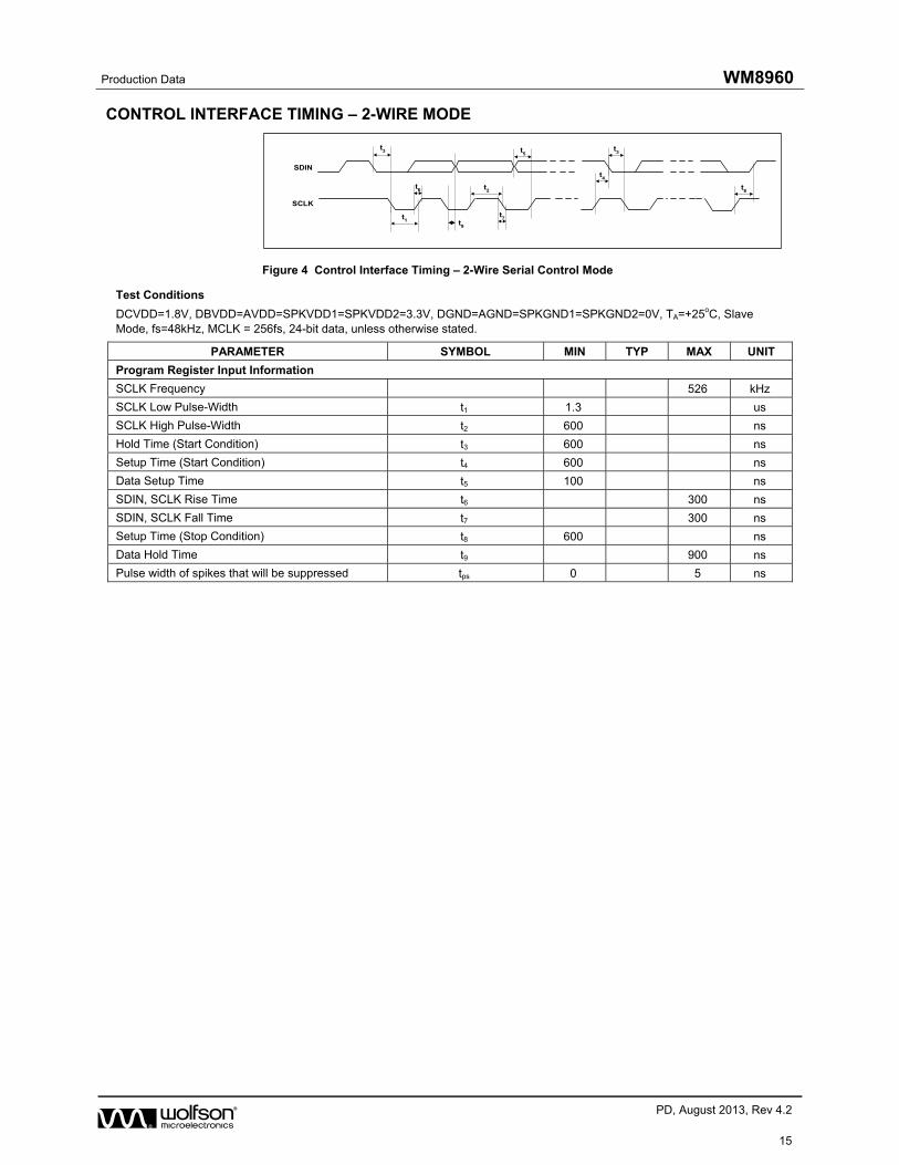
CONTROL INTERFACE TIMING – 2-WIRE MODE
SDIN
SCLK
t3
t1
t6 t2
t7
t5
t4
t3
t8
t9
Figure 4 Control Interface Timing – 2-Wire Serial Control Mode
Test Conditions
DCVDD=1.8V, DBVDD=AVDD=SPKVDD1=SPKVDD2=3.3V, DGND=AGND=SPKGND1=SPKGND2=0V, TA=+25oC, Slave Mode, fs=48kHz, MCLK = 256fs, 24-bit data, unless otherwise stated.
PARAMETER SYMBOL MIN TYP MAX UNIT
Program Register Input Information
SCLK Frequency 526 kHz
SCLK Low Pulse-Width t1 1.3 us
SCLK High Pulse-Width t2 600 ns
Hold Time (Start Condition) t3 600 ns
Setup Time (Start Condition) t4 600 ns
Data Setup Time t5 100 ns
SDIN, SCLK Rise Time t6 300 ns
SDIN, SCLK Fall Time t7 300 ns
Setup Time (Stop Condition) t8 600 ns
Data Hold Time t9 900 ns
Pulse width of spikes that will be suppressed tps 0 5 ns
WM8960 Production Data
w PD, August 2013, Rev 4.2
16
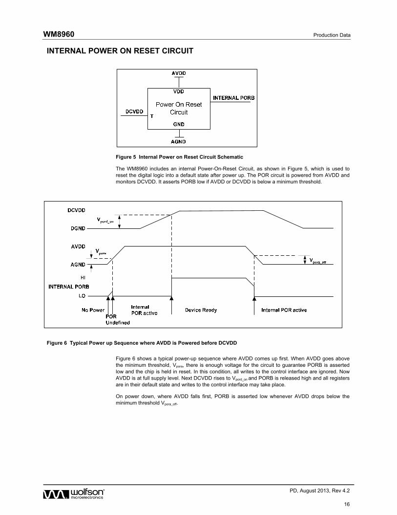
INTERNAL POWER ON RESET CIRCUIT
Figure 5 Internal Power on Reset Circuit Schematic
The WM8960 includes an internal Power-On-Reset Circuit, as shown in Figure 5, which is used to reset the digital logic into a default state after power up. The POR circuit is powered from AVDD and monitors DCVDD. It asserts PORB low if AVDD or DCVDD is below a minimum threshold.
Figure 6 Typical Power up Sequence where AVDD is Powered before DCVDD
Figure 6 shows a typical power-up sequence where AVDD comes up first. When AVDD goes above the minimum threshold, Vpora, there is enough voltage for the circuit to guarantee PORB is asserted low and the chip is held in reset. In this condition, all writes to the control interface are ignored. Now AVDD is at full supply level. Next DCVDD rises to Vpord_on and PORB is released high and all registers are in their default state and writes to the control interface may take place.
On power down, where AVDD falls first, PORB is asserted low whenever AVDD drops below the minimum threshold Vpora_off.

Production Data WM8960
w PD, August 2013, Rev 4.2
17
Figure 7 Typical Power up Sequence where DCVDD is Powered before AVDD
Figure 7 shows a typical power-up sequence where DCVDD comes up first. First it is assumed that DCVDD is already up to specified operating voltage. When AVDD goes above the minimum threshold, Vpora, there is enough voltage for the circuit to guarantee PORB is asserted low and the chip is held in reset. In this condition, all writes to the control interface are ignored. When AVDD rises to Vpora_on, PORB is released high and all registers are in their default state and writes to the control interface may take place.
On power down, where DCVDD falls first, PORB is asserted low whenever DCVDD drops below the minimum threshold Vpord_off.
SYMBOL MIN TYP MAX UNIT
Vpora 0.4 0.6 0.8 V
Vpora_on 0.9 1.2 1.6 V
Vpora_off 0.4 0.6 0.8 V
Vpord_on 0.5 0.7 0.9 V
Vpord_off 0.4 0.6 0.8 V
Table 1 Typical POR Operation (typical values, not tested)
Notes:
1. If AVDD and DCVDD suffer a brown-out (i.e. drop below the minimum recommended operating level but do not go below Vpora_off or Vpord_off) then the chip will not reset and will resume normal operation when the voltage is back to the recommended level again.
2. The chip will enter reset at power down when AVDD or DCVDD falls below Vpora_off or Vpord_off. This may be important if the supply is turned on and off frequently by a power management system.
3. The minimum tpor period is maintained even if DCVDD and AVDD have zero rise time. This specification is guaranteed by design rather than test.

WM8960 Production Data
w PD, August 2013, Rev 4.2
18
DEVICE DESCRIPTION
INTRODUCTION
The WM8960 is a low power audio CODEC offering a combination of high quality audio, advanced features, low power and small size. These characteristics make it ideal for portable digital audio applications with stereo speaker and headphone outputs such as games consoles, portable media players and multimedia phones.
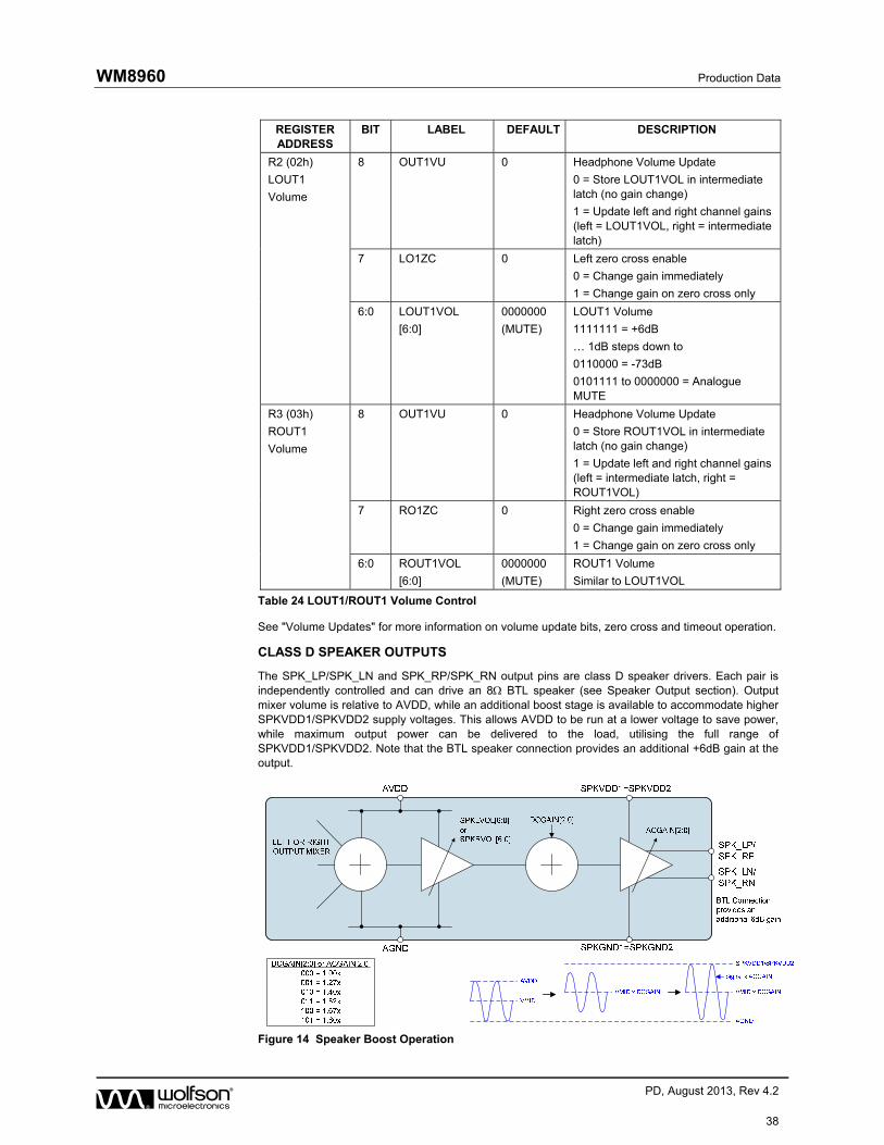
Stereo class D speaker drivers can provide >1W per channel into 8 loads. BTL configuration provides high power output and excellent PSRR. Low leakage and pop/click suppression mechanisms allow direct battery connection, reducing component count and power consumption in portable battery-powered applications. Highly flexible speaker boost settings provide fully internal level-shifting of analogue output signals, allowing speaker output power to be maximised while minimising other analogue supply currents, and requiring no additional components.
A flexible input configuration includes support for two stereo microphone interfaces (single-ended or pseudo-differential) and additional stereo line inputs. Up to three stereo analogue input sources are available, removing the need for external analogue switches in many applications. Boost amplifiers are available for additional gain on the microphone inputs and a programmable gain amplifier with a mixed signal automatic level control (ALC) keeps the recording volume constant.
The stereo ADC and DAC are of hi-fi quality using a 24-bit, low-order oversampling architecture to deliver optimum performance. A flexible clocking arrangement supports mixed ADC and DAC sample rates.
The DAC output signal can be mixed with analogue input signals from the line inputs or bypass paths. This mix is available on speaker and headphone/line outputs.
The WM8960 has a configurable digital audio interface where ADC data can be read and digital audio playback data fed to the DAC. It supports a number of audio data formats including I2S, DSP Mode (a burst mode in which frame sync plus two data packed words are transmitted), MSB-First, left justified and MSB-First, right justified, and can operate in master or slave modes. In PCM mode A-law and -law companding is supported.
The SYSCLK (system clock) provides clocking for the ADCs, DACs, DSP core, class D outputs and the digital audio interface. SYSCLK can be derived directly from the MCLK pin or via an integrated PLL, providing flexibility to support a wide range of clocking schemes. All MCLK frequencies typically used in portable systems are supported for sample rates between 8kHz and 48kHz. A flexible switching clock for the class D speaker drivers (synchronous with the audio DSP clocks for best performance) is also derived from SYSCLK.
To allow full software control over all its features, the WM8960 uses a 2 wire control interface. It is fully compatible and an ideal partner for a wide range of industry standard microprocessors, controllers and DSPs. Unused circuitry can be disabled via software to save power, while low leakage currents extend standby and off time in portable battery-powered applications.
Production Data WM8960
w PD, August 2013, Rev 4.2
19
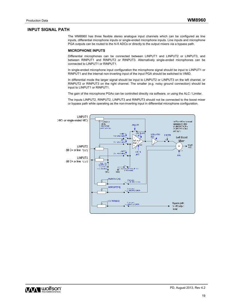
INPUT SIGNAL PATH
The WM8960 has three flexible stereo analogue input channels which can be configured as line inputs, differential microphone inputs or single-ended microphone inputs. Line inputs and microphone PGA outputs can be routed to the hi-fi ADCs or directly to the output mixers via a bypass path.
MICROPHONE INPUTS
Differential microphones can be connected between LINPUT1 and LINPUT2 or LINPUT3, and between RINPUT1 and RINPUT2 or RINPUT3. Alternatively single-ended microphones can be connected to LINPUT1 or RINPUT1.
In single-ended microphone input configuration the microphone signal should be input to LINPUT1 or RINPUT1 and the internal non-inverting input of the input PGA should be switched to VMID.
In differential mode the larger signal should be input to LINPUT2 or LINPUT3 on the left channel, or RINPUT2 or RINPUT3 on the right channel. The smaller (e.g. noisy ground connection) should be input to LINPUT1 or RINPUT1.
The gain of the microphone PGAs can be controlled directly via software, or using the ALC / Limiter.
The inputs LINPUT2, RINPUT2, LINPUT3 and RINPUT3 should not be connected to the boost mixer or bypass path while operating as the non-inverting input in differential microphone configuration.

WM8960 Production Data
w PD, August 2013, Rev 4.2
20
Figure 8 Microphone Input PGA Circuit
The input PGAs and boost mixers are enabled by the AINL and AINR register bits. The microphone PGAs can be also be disabled independently of the boost mixer to save power, using LMIC and RMIC register bits.
REGISTER ADDRESS
BIT LABEL DEFAULT DESCRIPTION
R25 (19h)
Power Management (1)
5 AINL 0 Left channel input PGA and boost stage enable
0 = PGA disabled, boost disabled
1 = PGA enabled (if LMIC = 1), boost enabled
4 AINR 0 Right channel input PGA and boost stage enable
0 = PGA disabled, boost disabled
1 = PGA enabled (if LMIC = 1), boost enabled
R47 (2Fh)
Power Management (3)
5 LMIC 0 Left channel input PGA enable
0 = PGA disabled
1 = PGA enabled (if AINL = 1)
4 RMIC 0 Right channel input PGA enable
0 = PGA disabled
1 = PGA enabled (if AINR = 1)
Table 2 Input PGA and Boost Enable Register Settings
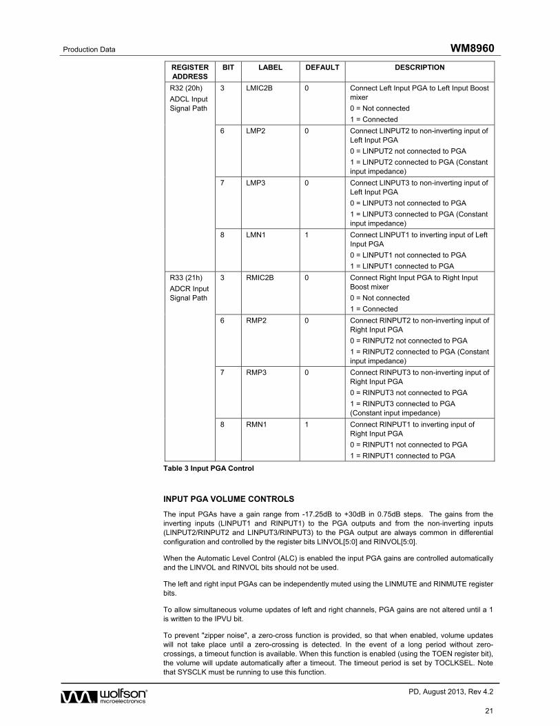
The input PGAs can be configured as differential inputs, using LINPUT1/LINPUT2 or LINPUT1/LINPUT3, and RINPUT1/RINPUT2 or RINPUT1/RINPUT3. The input impedance to these non-inverting inputs is constant in this configuration. Differential configuration is controlled by LMP2, LMP3, RMP2 and RMP3 as shown in Table 3.
When single-ended configuration is selected, the non-inverting input of the PGA is connected to VMID.
Production Data WM8960
w PD, August 2013, Rev 4.2
21
REGISTER ADDRESS
BIT LABEL DEFAULT DESCRIPTION
R32 (20h)
ADCL Input Signal Path
3 LMIC2B 0 Connect Left Input PGA to Left Input Boost mixer
0 = Not connected
1 = Connected
6 LMP2 0 Connect LINPUT2 to non-inverting input of Left Input PGA
0 = LINPUT2 not connected to PGA
1 = LINPUT2 connected to PGA (Constant input impedance)
7 LMP3 0 Connect LINPUT3 to non-inverting input of Left Input PGA
0 = LINPUT3 not connected to PGA
1 = LINPUT3 connected to PGA (Constant input impedance)
8 LMN1 1 Connect LINPUT1 to inverting input of Left Input PGA
0 = LINPUT1 not connected to PGA
1 = LINPUT1 connected to PGA
R33 (21h)
ADCR Input Signal Path
3 RMIC2B 0 Connect Right Input PGA to Right Input Boost mixer
0 = Not connected
1 = Connected
6 RMP2 0 Connect RINPUT2 to non-inverting input of Right Input PGA
0 = RINPUT2 not connected to PGA
1 = RINPUT2 connected to PGA (Constant input impedance)
7 RMP3 0 Connect RINPUT3 to non-inverting input of Right Input PGA
0 = RINPUT3 not connected to PGA
1 = RINPUT3 connected to PGA (Constant input impedance)
8 RMN1 1 Connect RINPUT1 to inverting input of Right Input PGA
0 = RINPUT1 not connected to PGA
1 = RINPUT1 connected to PGA
Table 3 Input PGA Control
INPUT PGA VOLUME CONTROLS
The input PGAs have a gain range from -17.25dB to +30dB in 0.75dB steps. The gains from the inverting inputs (LINPUT1 and RINPUT1) to the PGA outputs and from the non-inverting inputs (LINPUT2/RINPUT2 and LINPUT3/RINPUT3) to the PGA output are always common in differential configuration and controlled by the register bits LINVOL[5:0] and RINVOL[5:0].
When the Automatic Level Control (ALC) is enabled the input PGA gains are controlled automatically and the LINVOL and RINVOL bits should not be used.
The left and right input PGAs can be independently muted using the LINMUTE and RINMUTE register bits.
To allow simultaneous volume updates of left and right channels, PGA gains are not altered until a 1 is written to the IPVU bit.
To prevent "zipper noise", a zero-cross function is provided, so that when enabled, volume updates will not take place until a zero-crossing is detected. In the event of a long period without zero-crossings, a timeout function is available. When this function is enabled (using the TOEN register bit), the volume will update automatically after a timeout. The timeout period is set by TOCLKSEL. Note that SYSCLK must be running to use this function.

WM8960 Production Data
w PD, August 2013, Rev 4.2
22
REGISTER ADDRESS
BIT LABEL DEFAULT DESCRIPTION
R0 (00h)
Left Channel
PGA
8 IPVU N/A Input PGA Volume Update
Writing a 1 to this bit will cause left and right input PGA volumes to be updated (LINVOL and RINVOL)
7 LINMUTE 1 Left Input PGA Analogue Mute
1 = Enable Mute
0 = Disable Mute
Note: IPVU must be set to un-mute.
6 LIZC 0 Left Input PGA Zero Cross Detector
1 = Change gain on zero cross only
0 = Change gain immediately
5:0 LINVOL
[5:0]
010111
( 0dB )
Left Input PGA Volume Control
111111 = +30dB
111110 = +29.25dB
. . 0.75dB steps down to
000000 = -17.25dB
R1 (01h)
Right Channel
PGA
8 IPVU N/A Input PGA Volume Update
Writing a 1 to this bit will cause left and right input PGA volumes to be updated (LINVOL and RINVOL)
7 RINMUTE 1 Right Input PGA Analogue Mute
1 = Enable Mute
0 = Disable Mute
Note: IPVU must be set to un-mute.
6 RIZC 0 Right Input PGA Zero Cross Detector
1 = Change gain on zero cross only
0 = Change gain immediately
5:0 RINVOL
[5:0]
010111
( 0dB )
Right Input PGA Volume Control
111111 = +30dB
111110 = +29.25dB
. . 0.75dB steps down to
000000 = -17.25dB
R23 (17h)
Additional Control (1)
0 TOEN 0 Timeout Enable (Also enables jack detect debounce clock)
0 = Timeout disabled
1 = Timeout enabled
1 TOCLKSEL 0 Slow Clock Selection (Used for volume update timeouts and for jack detect debounce)
0 = SYSCLK / 221 (Slower Response)
1 = SYSCLK / 219 (Faster Response)
Table 4 Input PGA Volume Control
See "Volume Updates" for more information on volume update bits, zero cross and timeout operation.
LINE INPUTS
Two pairs of stereo line inputs (LINPUT2 / RINPUT2 and LINPUT3 / RINPUT3) are available as analogue inputs into the ADC path. LINPUT3 and RINPUT3 can also be input directly to the output mixers via the bypass paths.
See "Output Signal Path" for more information on the bypass paths.

Production Data WM8960
w PD, August 2013, Rev 4.2
23
INPUT BOOST
The input path to the ADCs is via a boost stage, which can mix signals from the microphone PGAs and the line inputs.
The boost stage can provide up to +29dB additional gain from the microphone PGA output to the ADC input, providing a total maximum available analogue gain of +59dB from microphone to ADC. The microphone PGA path to the boost mixer is muted using LINMUTE and RINMUTE as shown in Table 4. Microphone PGA to boost gain settings are shown in Table 5.
REGISTER ADDRESS
BIT LABEL DEFAULT DESCRIPTION
R32 (20h)
ADCL Signal path
5:4 LMICBOOST
[1:0]
00 Left Channel Input PGA Boost Gain
00 = +0dB
01 = +13dB
10 = +20dB
11 = +29dB
R33 (21h)
ADCR Signal path
5:4 RMICBOOST
[1:0]
00 Right Channel Input PGA Boost Gain
00 = +0dB
01 = +13dB
10 = +20dB
11 = +29dB
Table 5 Microphone PGA Boost Control
For line inputs, -12dB to +6dB gain is available on the boost mixer, with mute control, as shown in Table 6.
REGISTER ADDRESS
BIT LABEL DEFAULT DESCRIPTION
R43 (2Bh)
Input Boost Mixer 1
6:4 LIN3BOOST
[2:0]
000 LINPUT3 to Boost Mixer gain
000 = Mute
001 = -12dB
...3dB steps up to
111 = +6dB
3:1 LIN2BOOST
[2:0]
000 LINPUT2 to Boost Mixer gain
000 = Mute
001 = -12dB
...3dB steps up to
111 = +6dB
R44 (2Ch)
Input Boost Mixer 2
6:4 RIN3BOOST
[2:0]
000 RINPUT3 to Boost Mixer gain
000 = Mute
001 = -12dB
...3dB steps up to
111 = +6dB
3:1 RIN2BOOST
[2:0]
000 RINPUT2 to Boost Mixer gain
000 = Mute
001 = -12dB
...3dB steps up to
111 = +6dB
Table 6 Line Input Boost Control
When all three input paths to the boost mixer are disabled, the boost mixer will automatically be muted.

WM8960 Production Data
w PD, August 2013, Rev 4.2
24
MICROPHONE BIASING CIRCUIT
The MICBIAS output provides a low noise reference voltage suitable for biasing electret type microphones and the associated external resistor biasing network. Refer to the Applications Information section for recommended external components. The MICBIAS voltage can be altered via the MBSEL register bit. When MBSEL=0, MICBIAS=0.9*AVDD and when MBSEL=1, MICBIAS=0.65*AVDD. The output can be enabled or disabled using the MICB control bit.
REGISTER ADDRESS
BIT LABEL DEFAULT DESCRIPTION
R25 (19h)
Power management (1)
1 MICB 0 Microphone Bias Enable
0 = OFF (high impedance output)
1 = ON
R48 (30h)
Additional Control (4)
0 MBSEL 0 Microphone Bias Voltage Control
0 = 0.9 * AVDD
1 = 0.65 * AVDD
Table 7 Microphone Bias Control
The internal MICBIAS circuitry is shown in Figure 9. The maximum source current capability for MICBIAS is 3mA. The external biasing resistors therefore must be large enough to limit the MICBIAS current to 3mA.
Figure 9 Microphone Bias Schematic
Production Data WM8960
w PD, August 2013, Rev 4.2
25
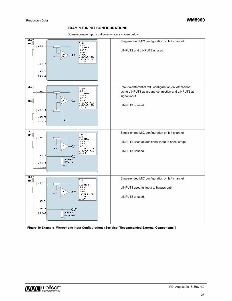
EXAMPLE INPUT CONFIGURATIONS
Some example input configurations are shown below.
Single-ended MIC configuration on left channel.
LINPUT2 and LINPUT3 unused
Pseudo-differential MIC configuration on left channel
using LINPUT1 as ground connection and LINPUT2 as
signal input.
LINPUT3 unused.
Single-ended MIC configuration on left channel.
LINPUT2 used as additional input to boost stage.
LINPUT3 unused.
Single-ended MIC configuration on left channel.
LINPUT3 used as input to bypass path.
LINPUT2 unused.
Figure 10 Example Microphone Input Configurations (See also "Recommended External Components")
WM8960 Production Data
w PD, August 2013, Rev 4.2
26
ANALOGUE TO DIGITAL CONVERTER (ADC)
The WM8960 uses stereo 24-bit, 64x oversampled sigma-delta ADCs. The use of multi-bit feedback and high oversampling rates reduce the effects of jitter and high frequency noise. The ADC Full Scale input level is proportional to AVDD. With a 3.3V supply voltage, the full scale level is 1.0Vrms. Any voltage greater than full scale may overload the ADC and cause distortion.
The ADCs are enabled by the ADCL/R register bit.
REGISTER ADDRESS
BIT LABEL DEFAULT DESCRIPTION
R25 (19h)
Power management (2)
3 ADCL 0 Enable ADC left channel:
0 = ADC disabled
1 = ADC enabled
2 ADCR 0 Enable ADC right channel:
0 = ADC disabled
1 = ADC enabled
Table 8 ADC Enable Control
The polarity of the output signal can be changed under software control using the ADCPOL[1:0] register bits. The DATSEL bits are used to select which channel is used for the left and right ADC data.
REGISTER ADDRESS
BIT LABEL DEFAULT DESCRIPTION
R5 (05h)
ADC and DAC Control (1)
6:5 ADCPOL[1:0] 00 ADC polarity control:
00 = Polarity not inverted
01 = ADC L inverted
10 = ADC R inverted
11 = ADC L and R inverted
R23 (17h)
Additional Control (1)
3:2 DATSEL
[1:0]
00 ADC Data Output Select
00: left data = left ADC;
right data =right ADC
01: left data = left ADC;
right data = left ADC
10: left data = right ADC;
right data =right ADC
11: left data = right ADC;
right data = left ADC
Table 9 ADC Control
DIGITAL ADC VOLUME CONTROL
The output of the ADCs can be digitally amplified or attenuated over a range from –97dB to +30dB in 0.5dB steps. The volume of each channel can be controlled separately. The gain for a given eight-bit code X is given by:
0.5 (X-195) dB for 1 X 255; MUTE for X = 0
The ADCVU control bit controls the loading of digital volume control data. When ADCVU is set to 0, the LADCVOL or RADCVOL control data will be loaded into the respective control register, but will not actually change the digital gain setting. Both left and right gain settings are updated when ADCVU is set to 1. This makes it possible to update the gain of both channels simultaneously.

Production Data WM8960
w PD, August 2013, Rev 4.2
27
REGISTER ADDRESS
BIT LABEL DEFAULT DESCRIPTION
R21 (15h)
Left ADC Digital Volume
7:0 LADCVOL
[7:0]
11000011
( 0dB )
Left ADC Digital Volume Control
0000 0000 = Digital Mute
0000 0001 = -97dB
0000 0010 = -96.5dB
... 0.5dB steps up to
1111 1111 = +30dB
8 ADCVU 0 ADC Volume Update
0 = Store LADCVOL in intermediate latch (no gain change)
1 = Update left and right channel gains (left = LADCVOL, right = intermediate latch)
R22 (16h)
Right ADC Digital Volume
7:0 RADCVOL
[7:0]
11000011
( 0dB )
Right ADC Digital Volume Control
0000 0000 = Digital Mute
0000 0001 = -97dB
0000 0010 = -96.5dB
... 0.5dB steps up to
1111 1111 = +30dB
8 ADCVU 0 ADC Volume Update
0 = Store RADCVOL in intermediate latch (no gain change)
1 = Update left and right channel gains (left = intermediate latch, right = RADCVOL)
Table 10 ADC Digital Volume Control
ADC DIGITAL FILTERS
The ADC filters perform true 24-bit signal processing to convert the raw multi-bit oversampled data from the ADC to the correct sampling frequency to be output on the digital audio interface.
HIGH PASS FILTER
A digital high pass filter is applied by default to the ADC path to remove DC offsets. This filter can be disabled using the ADCHPD register bit.
REGISTER ADDRESS
BIT LABEL DEFAULT DESCRIPTION
R5 (05h)
ADC and DAC Control (1)
0 ADCHPD 0 ADC High Pass Filter Disable
0 = Enable high pass filter on left and right channels
1 = Disable high pass filter on left and right channels
Table 11 ADC High Pass Filter
The high pass filter characteristics are shown in the Digital Filter Characteristics section.
WM8960 Production Data
w PD, August 2013, Rev 4.2
28
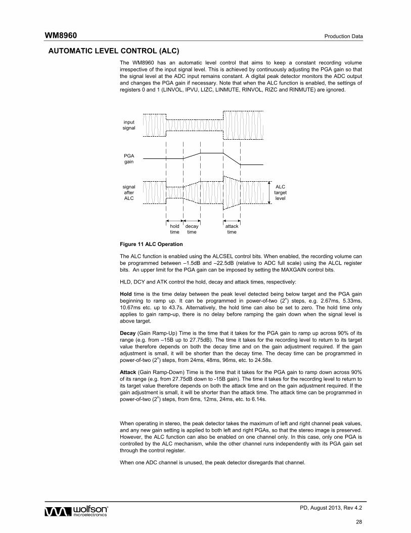
AUTOMATIC LEVEL CONTROL (ALC)
The WM8960 has an automatic level control that aims to keep a constant recording volume irrespective of the input signal level. This is achieved by continuously adjusting the PGA gain so that the signal level at the ADC input remains constant. A digital peak detector monitors the ADC output and changes the PGA gain if necessary. Note that when the ALC function is enabled, the settings of registers 0 and 1 (LINVOL, IPVU, LIZC, LINMUTE, RINVOL, RIZC and RINMUTE) are ignored.
holdtime
decaytime
attacktime
inputsignal
signalafterALC
PGAgain
ALCtargetlevel
Figure 11 ALC Operation
The ALC function is enabled using the ALCSEL control bits. When enabled, the recording volume can be programmed between –1.5dB and –22.5dB (relative to ADC full scale) using the ALCL register bits. An upper limit for the PGA gain can be imposed by setting the MAXGAIN control bits.
HLD, DCY and ATK control the hold, decay and attack times, respectively:
Hold time is the time delay between the peak level detected being below target and the PGA gain beginning to ramp up. It can be programmed in power-of-two (2n) steps, e.g. 2.67ms, 5.33ms, 10.67ms etc. up to 43.7s. Alternatively, the hold time can also be set to zero. The hold time only applies to gain ramp-up, there is no delay before ramping the gain down when the signal level is above target.
Decay (Gain Ramp-Up) Time is the time that it takes for the PGA gain to ramp up across 90% of its range (e.g. from –15B up to 27.75dB). The time it takes for the recording level to return to its target value therefore depends on both the decay time and on the gain adjustment required. If the gain adjustment is small, it will be shorter than the decay time. The decay time can be programmed in power-of-two (2n) steps, from 24ms, 48ms, 96ms, etc. to 24.58s.
Attack (Gain Ramp-Down) Time is the time that it takes for the PGA gain to ramp down across 90% of its range (e.g. from 27.75dB down to -15B gain). The time it takes for the recording level to return to its target value therefore depends on both the attack time and on the gain adjustment required. If the gain adjustment is small, it will be shorter than the attack time. The attack time can be programmed in power-of-two (2n) steps, from 6ms, 12ms, 24ms, etc. to 6.14s.
When operating in stereo, the peak detector takes the maximum of left and right channel peak values, and any new gain setting is applied to both left and right PGAs, so that the stereo image is preserved. However, the ALC function can also be enabled on one channel only. In this case, only one PGA is controlled by the ALC mechanism, while the other channel runs independently with its PGA gain set through the control register.
When one ADC channel is unused, the peak detector disregards that channel.
Production Data WM8960
w PD, August 2013, Rev 4.2
29
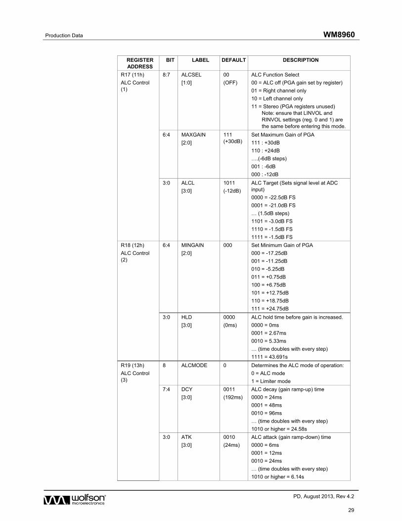
REGISTER ADDRESS
BIT LABEL DEFAULT DESCRIPTION
R17 (11h)
ALC Control (1)
8:7 ALCSEL
[1:0]
00
(OFF)
ALC Function Select
00 = ALC off (PGA gain set by register)
01 = Right channel only
10 = Left channel only
11 = Stereo (PGA registers unused) Note: ensure that LINVOL and RINVOL settings (reg. 0 and 1) are the same before entering this mode.
6:4 MAXGAIN
[2:0]
111 (+30dB)
Set Maximum Gain of PGA
111 : +30dB
110 : +24dB
….(-6dB steps)
001 : -6dB
000 : -12dB
3:0 ALCL
[3:0]
1011
(-12dB)
ALC Target (Sets signal level at ADC input)
0000 = -22.5dB FS
0001 = -21.0dB FS
… (1.5dB steps)
1101 = -3.0dB FS
1110 = -1.5dB FS
1111 = -1.5dB FS
R18 (12h)
ALC Control (2)
6:4 MINGAIN
[2:0]
000 Set Minimum Gain of PGA
000 = -17.25dB
001 = -11.25dB
010 = -5.25dB
011 = +0.75dB
100 = +6.75dB
101 = +12.75dB
110 = +18.75dB
111 = +24.75dB
3:0 HLD
[3:0]
0000
(0ms)
ALC hold time before gain is increased.
0000 = 0ms
0001 = 2.67ms
0010 = 5.33ms
… (time doubles with every step)
1111 = 43.691s
R19 (13h)
ALC Control (3)
8 ALCMODE 0 Determines the ALC mode of operation:
0 = ALC mode
1 = Limiter mode
7:4 DCY
[3:0]
0011
(192ms)
ALC decay (gain ramp-up) time
0000 = 24ms
0001 = 48ms
0010 = 96ms
… (time doubles with every step)
1010 or higher = 24.58s
3:0 ATK
[3:0]
0010
(24ms)
ALC attack (gain ramp-down) time
0000 = 6ms
0001 = 12ms
0010 = 24ms
… (time doubles with every step)
1010 or higher = 6.14s

WM8960 Production Data
w PD, August 2013, Rev 4.2
30
REGISTER ADDRESS
BIT LABEL DEFAULT DESCRIPTION
R27 (1Bh)
Additional Control (3)
2:0 ADC_ALC_SR
[2:0]
000 ALC Sample Rate
000 = 44.1k / 48k
001 = 32k
010 = 22.05k / 24k
011 = 16k
100 = 11.25k / 12k
101 = 8k
110 and 111 = Reserved
Table 12 ALC Control
ALC SAMPLE RATE CONTROL
The register bits ADC_ALC_SR must be set correctly to ensure that the ALC attack, decay and hold times are correct for the chosen sample rate as shown in Table 12.
PEAK LIMITER
To prevent clipping when a large signal occurs just after a period of quiet, the ALC circuit includes a limiter function. If the ADC input signal exceeds 87.5% of full scale (–1.16dB), the PGA gain is ramped down at the maximum attack rate (as when ATK = 0000), until the signal level falls below 87.5% of full scale. This function is automatically enabled whenever the ALC is enabled.
Note:
If ATK = 0000, then the limiter makes no difference to the operation of the ALC. It is designed to prevent clipping when long attack times are used.
NOISE GATE
When the signal is very quiet and consists mainly of noise, the ALC function may cause “noise pumping”, i.e. loud hissing noise during silence periods. The WM8960 has a noise gate function that prevents noise pumping by comparing the signal level at the input pins against a noise gate threshold, NGTH. The noise gate cuts in when:
Signal level at ADC [dB] < NGTH [dB] + PGA gain [dB] + Mic Boost gain [dB]
This is equivalent to:
Signal level at input pin [dB] < NGTH [dB]
The PGA gain will then be held constant (preventing it from ramping up as it normally would when the signal is quiet).
The table below summarises the noise gate control register. The NGTH control bits set the noise gate threshold with respect to the ADC full-scale range. The threshold is adjusted in 1.5dB steps. Levels at the extremes of the range may cause inappropriate operation, so care should be taken with set–up of the function. Note that the noise gate only works in conjunction with the ALC function, and always operates on the same channel(s) as the ALC (left, right, both, or none).
REGISTER ADDRESS
BIT LABEL DEFAULT DESCRIPTION
R20 (14h)
Noise Gate
Control
7:3 NGTH
[4:0]
00000 Noise gate threshold
00000 -76.5dBfs
00001 -75dBfs
… 1.5 dB steps
11110 -31.5dBfs
11111 -30dBfs
0 NGAT 0 Noise gate function enable
0 = disable
1 = enable
Table 13 Noise Gate Control

Production Data WM8960
w PD, August 2013, Rev 4.2
31
OUTPUT SIGNAL PATH
The hi-fi DACs and DAC digital filters are enabled by register bits DACL and DACR. The mixers and output drivers can be separately enabled by individual control bits (see Analogue Outputs). Thus it is possible to utilise the analogue mixing and amplification provided by the WM8960, irrespective of whether the DACs are enabled or not.
The WM8960 DACs receive digital input data on the DACDAT pin. The digital filter block processes the data to provide the following functions:
Digital volume control with soft mute and soft un-mute
Mono mix
3D stereo enhancement
De-emphasis
Sigma-delta modulation
High performance sigma-delta 24-bit audio DAC converts the digital data into an analogue signal.
The analogue outputs from the DACs can then be mixed with the analogue line inputs and the ADC analogue inputs. This mix is fed to the output drivers for headphone or speaker output. OUT3 can provide a mono mix of left and right mixers or a pseudo-ground for capless headphone drive.
DIGITAL PLAYBACK (DAC) PATH
Digital data is passed to the WM8960 via the flexible audio interface to the hi-fi DACs. The DACs are enabled by the DACL and DACR register bits.
REGISTER ADDRESS
BIT LABEL DEFAULT DESCRIPTION
R26 (1Ah)
Power Management (2)
8 DACL 0 Left Channel DAC Enable
0 = DAC disabled
1 = DAC enabled
7 DACR 0 Right Channel DAC Enable
0 = DAC disabled
1 = DAC enabled
Table 14 DAC Enable Control
DIGITAL DAC VOLUME CONTROL
The signal volume from each DAC can be controlled digitally, in the same way as the ADC volume (see Digital ADC Volume Control). The gain and attenuation range is –127dB to 0dB in 0.5dB steps. The level of attenuation for an eight-bit code X is given by:
0.5 (X-255) dB for 1 X 255; MUTE for X = 0
The DACVU control bit controls the loading of digital volume control data. When DACVU is set to 0, the LDACVOL or RDACVOL control data is loaded into an intermediate register, but the actual gain does not change. Both left and right gain settings are updated simultaneously when DACVU is set to 1.
See "Volume Updates" for more information on volume update bits.
WM8960 Production Data
w PD, August 2013, Rev 4.2
32
REGISTER ADDRESS
BIT LABEL DEFAULT DESCRIPTION
R10 (0Ah)
Left Channel Digital Volume
8 DACVU 0 DAC Volume Update
0 = Store LDACVOL in intermediate latch (no gain change)
1 = Update left and right channel gains (left = LDACVOL, right = intermediate latch)
7:0 LDACVOL
[7:0]
11111111
( 0dB )
Left DAC Digital Volume Control
0000 0000 = Digital Mute
0000 0001 = -127dB
0000 0010 = -126.5dB
... 0.5dB steps up to
1111 1111 = 0dB
R11 (0Bh)
Right Channel Digital Volume
8 DACVU 0 DAC Volume Update
0 = Store RDACVOL in intermediate latch (no gain change)
1 = Update left and right channel gains (left = intermediate latch, right = RDACVOL)
7:0 RDACVOL
[7:0]
11111111
( 0dB )
Right DAC Digital Volume Control
similar to LDACVOL
Table 15 Digital Volume Control
DAC SOFT MUTE AND SOFT UN-MUTE
The WM8960 also has a soft mute function, which, when enabled, gradually attenuates the volume of the digital signal to zero. When soft mute is disabled, the gain will either gradually ramp back up to the digital gain setting, or return instantly to the digital gain setting, depending on the DACSMM register bit.
The DAC is soft-muted by default. To play back an audio signal, this function must first be disabled by setting the DACMU bit to zero.
DACSMM would typically be enabled when using soft mute during playback of audio data so that when soft mute is then disabled, the sudden volume increase will not create pop noise by jumping immediately to the previous volume level (e.g. resuming playback after pausing during a track).
DACSMM would typically be disabled when un-muting at the start of a digital music file, so that the first part of the track is not attenuated (e.g. when starting playback of a new track, or resuming playback after pausing between tracks).
DAC muting and un-muting using volume control bits LDACVOL and RDACVOL.
DAC muting and un-muting using soft mute bit DACMU.
Soft un-mute not enabled (DACSMM = 0).
DAC muting and un-muting using soft mute bit DACMU.
Soft un-mute enabled (DACSMM = 1).
Figure 12 DAC Mute Control
The volume ramp rate during soft mute and un-mute is controlled by the DACMR bit. Ramp rates of fs/32 and fs/2 are selectable as shown in Table 16 (fs = DAC sample rate).

Production Data WM8960
w PD, August 2013, Rev 4.2
33
REGISTER ADDRESS
BIT LABEL DEFAULT DESCRIPTION
R5 (05h)
ADC and DAC Control (1)
3 DACMU 1 Digital Soft Mute
1 = Mute
0 = No mute (signal active)
R6 (06h)
ADC and DAC Control (2)
3 DACSMM 0 DAC Soft Mute Mode
0 = Disabling soft-mute (DACMU=0) will cause the volume to change immediately to the LDACVOL / RDACVOL settings
1 = Disabling soft-mute (DACMU=0) will cause the volume to ramp up gradually to the LDACVOL / RDACVOL settings
2 DACMR 0 DAC Soft Mute Ramp Rate
0 = Fast ramp (fs/2 at fs=48k, providing maximum delay of 10.7ms)
1 = Slow ramp (fs/32 at fs=48k, providing maximum delay of 171ms)
Table 16 DAC Soft-Mute Control
DAC DE-EMPHASIS
Digital de-emphasis can be applied to the DAC playback data (e.g. when the data comes from a CD with pre-emphasis used in the recording). De-emphasis filtering is available for sample rates of 48kHz, 44.1kHz and 32kHz.
REGISTER ADDRESS
BIT LABEL DEFAULT DESCRIPTION
R5 (05h)
ADC and DAC Control (1)
2:1 DEEMPH
[1:0]
00 De-Emphasis Control
11 = 48kHz sample rate
10 = 44.1kHz sample rate
01 = 32kHz sample rate
00 = No de-emphasis
Table 17 DAC De-Emphasis Control
DAC OUTPUT PHASE AND MONO MIXING
The digital audio data is converted to oversampled bit streams in the on-chip, true 24-bit digital interpolation filters. The bitstream data enters two multi-bit, sigma-delta DACs, which convert them to high quality analogue audio signals. The multi-bit DAC architecture reduces high frequency noise and sensitivity to clock jitter. It also uses a Dynamic Element Matching technique for high linearity and low distortion.
In normal operation, the left and right channel digital audio data is converted to analogue in two separate DACs. There is a mono-mix mode where the two audio channels are mixed together digitally and then converted to analogue using only one DAC, while the other DAC is switched off. The mono-mix signal can be selected to appear on both analogue output channels. The mono mix is automatically attenuated by 6dB to prevent clipping.
The DAC output defaults to non-inverted. Setting DACPOL[0] bit will invert the left DAC output phase and setting DACPOL[1] bit will invert the right DAC output phase.
WM8960 Production Data
w PD, August 2013, Rev 4.2
34
REGISTER ADDRESS
BIT LABEL DEFAULT DESCRIPTION
R6 (06h)
ADC and DAC Control (2)
6:5 DACPOL[1:0] 00 DAC Polarity Control:
00 = Polarity not inverted
01 = DAC L inverted
10 = DAC R inverted
11 = DAC L and R inverted
R23 (17h)
Additional Control (1)
4 DMONOMIX 0 DAC Mono Mix
0 = Stereo
1 = Mono (Mono MIX output on enabled DACs)
Table 18 DAC Mono Mix and Phase Invert Select
3D STEREO ENHANCEMENT
The WM8960 has a digital 3D enhancement option to artificially increase the separation between the left and right channels. This effect can only be used for playback, not for record.
The 3D enhancement function is activated by the 3DEN bit, and the 3DDEPTH setting controls the degree of stereo expansion. Additionally, one of four filter characteristics can be selected for the 3D processing, using the 3DUC and 3DLC control bits.
REGISTER ADDRESS
BIT LABEL DEFAULT DESCRIPTION
R16 (10h)
3D enhance
6 3DUC 0 Upper Cut-Off Frequency
0 = High (Recommended for fs>=32kHz)
1 = Low (Recommended for fs<32kHz)
5 3DLC 0 Lower Cut-Off Frequency
0 = Low (Recommended for fs>=32kHz)
1 = High (Recommended for fs<32kHz)
4:1 3DDEPTH
[3:0]
0000 3D Stereo Depth
0000 = 0% (minimum 3D effect)
0001 = 6.67%
....
1110 = 93.3%
1111 = 100% (maximum 3D effect)
0 3DEN 0 3D Stereo Enhancement Enable
0 = Disabled
1 = Enabled
Table 19 3D Stereo Enhancement Function
When 3D enhancement is enabled it may be necessary to attenuate the signal by 6dB to avoid limiting. This is a user-selectable function, enabled by setting DACDIV2.
REGISTER ADDRESS
BIT LABEL DEFAULT DESCRIPTION
R5 (05h)
ADC and DAC control (1)
7 DACDIV2 0 DAC 6dB attenuate enable
0 = disabled (0dB)
1 = -6dB enabled
Table 20 DAC 6dB Attenuation Select
Production Data WM8960
w PD, August 2013, Rev 4.2
35
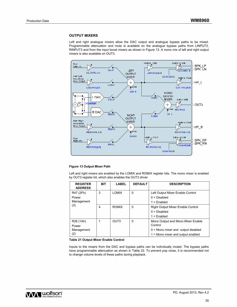
OUTPUT MIXERS
Left and right analogue mixers allow the DAC output and analogue bypass paths to be mixed. Programmable attenuation and mute is available on the analogue bypass paths from LINPUT3, RINPUT3 and from the input boost mixers as shown in Figure 13. A mono mix of left and right output mixers is also available on OUT3.
Figure 13 Output Mixer Path
Left and right mixers are enabled by the LOMIX and ROMIX register bits. The mono mixer is enabled by OUT3 register bit, which also enables the OUT3 driver.
REGISTER ADDRESS
BIT LABEL DEFAULT DESCRIPTION
R47 (2Fh)
Power Management (3)
3 LOMIX 0 Left Output Mixer Enable Control
0 = Disabled
1 = Enabled
4 ROMIX 0 Right Output Mixer Enable Control
0 = Disabled
1 = Enabled
R26 (1Ah)
Power Management (2)
1 OUT3 0 Mono Output and Mono Mixer Enable Control
0 = Mono mixer and output disabled
1 = Mono mixer and output enabled
Table 21 Output Mixer Enable Control
Inputs to the mixers from the DAC and bypass paths can be individually muted. The bypass paths have programmable attenuation as shown in Table 22. To prevent pop noise, it is recommended not to change volume levels of these paths during playback.
WM8960 Production Data
w PD, August 2013, Rev 4.2
36
REGISTER ADDRESS
BIT LABEL DEFAULT DESCRIPTION
R34 (22h)
Left Output Mixer Control
8 LD2LO 0 Left DAC to Left Output Mixer
0 = Disable (Mute)
1 = Enable Path
7 LI2LO 0 LINPUT3 to Left Output Mixer
0 = Disable (Mute)
1 = Enable Path
6:4 LI2LOVOL
[2:0]
101
(-15dB)
LINPUT3 to Left Output Mixer Volume
000 = 0dB
...(3dB steps)
111 = -21dB
R45 (2Dh)
Bypass (1)
7 LB2LO 0 Left Input Boost Mixer to Left Output Mixer
0 = Disable (Mute)
1 = Enable Path
6:4 LB2LOVOL
[2:0]
101
(-15dB)
Left Input Boost Mixer to Left Output Mixer Volume
000 = 0dB
...(3dB steps)
111 = -21dB
R37 (25h)
Right Output Mixer Control
8 RD2RO 0 Right DAC to Right Output Mixer
0 = Disable (Mute)
1 = Enable Path
7 RI2RO 0 RINPUT3 to Right Output Mixer
0 = Disable (Mute)
1 = Enable Path
6:4 RI2ROVOL
[2:0]
101
(-15dB)
RINPUT3 to Right Output Mixer Volume
000 = 0dB
...(3dB steps)
111 = -21dB
R46 (2Eh)
Bypass (2)
7 RB2RO 0 Right Input Boost Mixer to Right Output Mixer
0 = Disable (Mute)
1 = Enable Path
6:4 RB2ROVOL
[2:0]
101
(-15dB)
Right Input Boost Mixer to Right Output Mixer Volume
000 = 0dB
...(3dB steps)
111 = -21dB
Table 22 Left and Right Output Mixer Mute and Volume Control
The mono output mixer can output, left, right, left+right or a buffered VMID. 0dB or 6dB attenuation is selectable using MOUTVOL register bit. It is recommended to attenuate a mono mix of left and right channels by 6dB in order to prevent clipping. This attenuation control (MOUTVOL) should not be modified while OUT3 is enabled as this may cause an audible click noise.

Production Data WM8960
w PD, August 2013, Rev 4.2
37
REGISTER ADDRESS
BIT LABEL DEFAULT DESCRIPTION
R38 (26h)
Mono Out Mix (1)
7 L2MO 0 Left Output Mixer to Mono Output Mixer Control
0 = Left channel mix disabled
1 = Left channel mix enabled
R39 (27h)
Mono Out Mix (2)
7 R2MO 0 Right Output Mixer to Mono Output Mixer Control
0 = Right channel mix disabled
1 = Right channel mix enabled
R42 (2Ah)
Mono Out Volume
6 MOUTVOL 1 Mono Output Mixer Volume Control
0 = 0dB
1 = -6dB
Table 23 Output Mixer Enable Control
When left and right inputs to the mono mixer are both disabled, the mono mixer will output VMID.
ANALOGUE OUTPUTS
HP_L AND HP_R OUTPUTS
The HP_L and HP_R pins can drive a 16 or 32 headphone or a line output (see Headphone Output and Line Output sections, respectively). The signal volume on HP_L and HP_R can be independently adjusted under software control by writing to LOUT1VOL and ROUT1VOL, respectively. Note that gains over 0dB may cause clipping if the signal is large. Any gain setting below 0101111 (minimum) mutes the output driver. The corresponding output pin remains at the same DC level (the reference voltage on the VREF pin), so that no click noise is produced when muting or un-muting.
A zero cross detect on the analogue output may also be enabled when changing the gain setting to minimize audible clicks and zipper noise as the gain updates. If zero cross is enabled a timeout is also available to update the gain if a zero cross does not occur. This function may be enabled by setting TOEN in register R23 (17h). The timeout period is set by TOCLKSEL. Note: SYSCLK must be enabled to use this function.
WM8960 Production Data
w PD, August 2013, Rev 4.2
38
REGISTER ADDRESS
BIT LABEL DEFAULT DESCRIPTION
R2 (02h)
LOUT1
Volume
8 OUT1VU 0 Headphone Volume Update
0 = Store LOUT1VOL in intermediate latch (no gain change)
1 = Update left and right channel gains (left = LOUT1VOL, right = intermediate latch)
7 LO1ZC 0 Left zero cross enable
0 = Change gain immediately
1 = Change gain on zero cross only
6:0 LOUT1VOL
[6:0]
0000000
(MUTE)
LOUT1 Volume
1111111 = +6dB
… 1dB steps down to
0110000 = -73dB
0101111 to 0000000 = Analogue MUTE
R3 (03h)
ROUT1
Volume
8 OUT1VU 0 Headphone Volume Update
0 = Store ROUT1VOL in intermediate latch (no gain change)
1 = Update left and right channel gains (left = intermediate latch, right = ROUT1VOL)
7 RO1ZC 0 Right zero cross enable
0 = Change gain immediately
1 = Change gain on zero cross only
6:0 ROUT1VOL
[6:0]
0000000
(MUTE)
ROUT1 Volume
Similar to LOUT1VOL
Table 24 LOUT1/ROUT1 Volume Control
See "Volume Updates" for more information on volume update bits, zero cross and timeout operation.
CLASS D SPEAKER OUTPUTS
The SPK_LP/SPK_LN and SPK_RP/SPK_RN output pins are class D speaker drivers. Each pair is independently controlled and can drive an 8 BTL speaker (see Speaker Output section). Output mixer volume is relative to AVDD, while an additional boost stage is available to accommodate higher SPKVDD1/SPKVDD2 supply voltages. This allows AVDD to be run at a lower voltage to save power, while maximum output power can be delivered to the load, utilising the full range of SPKVDD1/SPKVDD2. Note that the BTL speaker connection provides an additional +6dB gain at the output.
Figure 14 Speaker Boost Operation
Production Data WM8960
w PD, August 2013, Rev 4.2
39
REGISTER ADDRESS
BIT LABEL DEFAULT DESCRIPTION
R40 (28h)
Left Speaker
Volume
6:0 SPKLVOL
[6:0]
0000000
(MUTE)
SPK_LP/SPK_LN Volume
1111111 = +6dB
… 1dB steps down to
0110000 = -73dB
0101111 to 0000000 = Analogue MUTE
7 SPKLZC 0 Left Speaker Zero Cross Enable
1 = Change gain on zero cross only
0 = Change gain immediately
8 SPKVU 0 Speaker Volume Update
0 = Store SPKLVOL in intermediate latch (no gain change)
1 = Update left and right channel gains (left = SPKLVOL, right = intermediate latch)
R41 (29h)
Right Speaker
Volume
6:0 SPKRVOL
[6:0]
0000000
(MUTE)
SPK_RP/SPK_RN Volume
1111111 = +6dB
… 1dB steps down to
0110000 = -73dB
0101111 to 0000000 = Analogue MUTE
7 SPKRZC 0 Right Speaker Zero Cross Enable
1 = Change gain on zero cross only
0 = Change gain immediately
8 SPKVU 0 Speaker Volume Update
0 = Store SPKRVOL in intermediate latch (no gain change)
1 = Update left and right channel gains (left = intermediate latch, right = SPKRVOL)
R51 (33h)
Class D Control (3)
5:3 DCGAIN
[2:0]
000
(1.0x)
DC Speaker Boost (Boosts speaker DC output level by up to 1.8 x on left and right channels)
000 = 1.00x boost (+0dB)
001 = 1.27x boost (+2.1dB)
010 = 1.40x boost (+2.9dB)
011 = 1.52x boost (+3.6dB)
100 = 1.67x boost (+4.5dB)
101 = 1.8x boost (+5.1dB)
110 to 111 = Reserved
2:0 ACGAIN
[2:0]
000
(1.0x)
AC Speaker Boost (Boosts speaker AC output signal by up to 1.8 x on left and right channels)
000 = 1.00x boost (+0dB)
001 = 1.27x boost (+2.1dB)
010 = 1.40x boost (+2.9dB)
011 = 1.52x boost (+3.6dB)
100 = 1.67x boost (+4.5dB)
101 = 1.8x boost (+5.1dB)
110 to 111 = Reserved
Table 25 SPK_L/SPK_R Volume and Speaker Boost Control
To prevent pop noise, DCGAIN and ACGAIN should not be modified while the speaker outputs are enabled.
To avoid clipping at speaker ground, ACGAIN should not be greater than DCGAIN.

WM8960 Production Data
w PD, August 2013, Rev 4.2
40
To avoid clipping at speaker supply, SPKVDD1 and SPKVDD2 must be high enough to support the peak output voltage when using DCGAIN and ACGAIN functions. The peak output voltage is AVDD*(DCGAIN+ACGAIN)/2.
DCGAIN should normally be set to the same value as ACGAIN.
See "Volume Updates" for more information on volume update bits, zero cross and timeout operation.
See "Class D Speaker Outputs" for more information on class D speaker operation.
OUT3 OUTPUT
The OUT3 pin can drive a 16 or 32 headphone or a line output or be used as a pseudo-ground for capless headphone drive (see Headphone Output section). It can also drive out a mono mix of left and right output mixers (See Output Signal Path).
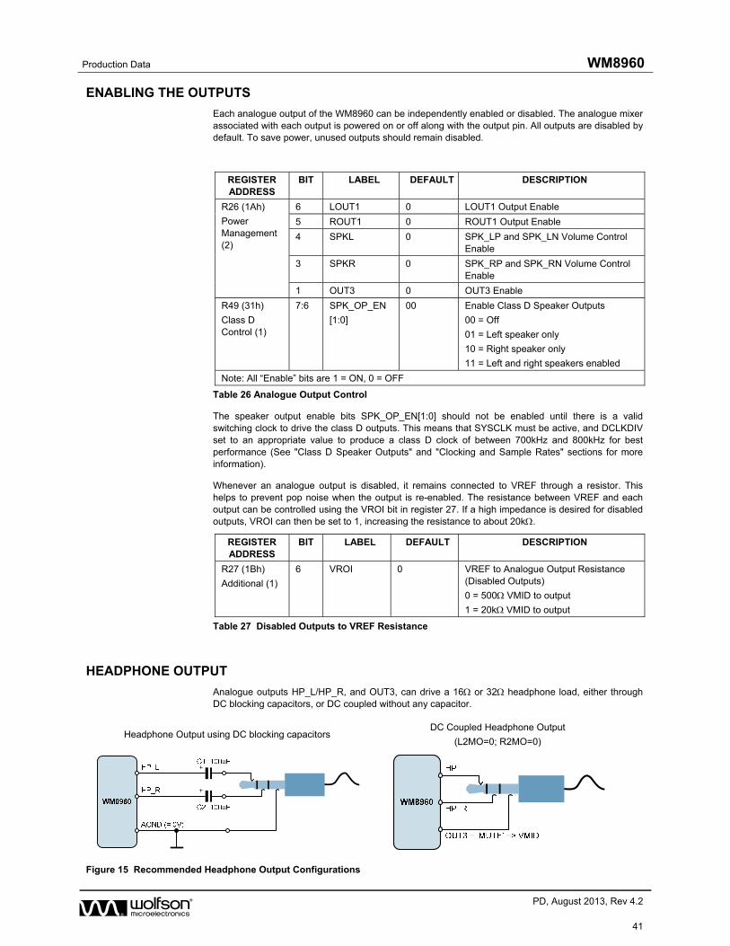
Production Data WM8960
w PD, August 2013, Rev 4.2
41
ENABLING THE OUTPUTS
Each analogue output of the WM8960 can be independently enabled or disabled. The analogue mixer associated with each output is powered on or off along with the output pin. All outputs are disabled by default. To save power, unused outputs should remain disabled.
REGISTER ADDRESS
BIT LABEL DEFAULT DESCRIPTION
R26 (1Ah)
Power Management (2)
6 LOUT1 0 LOUT1 Output Enable
5 ROUT1 0 ROUT1 Output Enable
4 SPKL 0 SPK_LP and SPK_LN Volume Control Enable
3 SPKR 0 SPK_RP and SPK_RN Volume Control Enable
1 OUT3 0 OUT3 Enable
R49 (31h)
Class D Control (1)
7:6 SPK_OP_EN
[1:0]
00 Enable Class D Speaker Outputs
00 = Off
01 = Left speaker only
10 = Right speaker only
11 = Left and right speakers enabled
Note: All “Enable” bits are 1 = ON, 0 = OFF
Table 26 Analogue Output Control
The speaker output enable bits SPK_OP_EN[1:0] should not be enabled until there is a valid switching clock to drive the class D outputs. This means that SYSCLK must be active, and DCLKDIV set to an appropriate value to produce a class D clock of between 700kHz and 800kHz for best performance (See "Class D Speaker Outputs" and "Clocking and Sample Rates" sections for more information).
Whenever an analogue output is disabled, it remains connected to VREF through a resistor. This helps to prevent pop noise when the output is re-enabled. The resistance between VREF and each output can be controlled using the VROI bit in register 27. If a high impedance is desired for disabled outputs, VROI can then be set to 1, increasing the resistance to about 20k.
REGISTER ADDRESS
BIT LABEL DEFAULT DESCRIPTION
R27 (1Bh)
Additional (1)
6 VROI 0 VREF to Analogue Output Resistance (Disabled Outputs)
0 = 500 VMID to output
1 = 20k VMID to output
Table 27 Disabled Outputs to VREF Resistance
HEADPHONE OUTPUT
Analogue outputs HP_L/HP_R, and OUT3, can drive a 16 or 32 headphone load, either through DC blocking capacitors, or DC coupled without any capacitor.
Headphone Output using DC blocking capacitors DC Coupled Headphone Output
(L2MO=0; R2MO=0)
Figure 15 Recommended Headphone Output Configurations
WM8960 Production Data
w PD, August 2013, Rev 4.2
42
When DC blocking capacitors are used, then their capacitance and the load resistance together determine the lower cut-off frequency, fc. Increasing the capacitance lowers fc, improving the bass response. Smaller capacitance values will diminish the bass response. Assuming a 32 load and C1, C2 = 100F:
fc = 1 / 2 RLC1 = 1 / (2 x 32 x 100F) = 50 Hz
In the DC coupled configuration, the headphone “ground” is connected to the OUT3 pin, which must be enabled by setting OUT3 = 1 and muted by setting L2MO=0 and R2MO=0. As the OUT3 pin produces a DC voltage of AVDD/2 (=VREF), there is no DC offset between HP_L/HP_R and OUT3, and therefore no DC blocking capacitors are required. This saves space and material cost in portable applications.
It is recommended to connect the DC coupled headphone outputs only to headphones, and not to the line input of another device. Although the built-in short circuit protection will prevent any damage to the headphone outputs, such a connection may be noisy, and may not function properly if the other device is grounded.
CLASS D SPEAKER OUTPUTS
The class D speaker outputs SPK_LN/SPK_LP and SPK_RN/SPK_RP can drive 1W into 8 BTL speakers. Class D outputs reduce power consumption and maximise efficiency by reducing power dissipated in the output drivers, delivering most of the power directly to the load. This is achieved by pulse width modulation (PWM) of a high frequency square wave, allowing the audio signal level to be set by controlling the pulse width. The frequency of the output waveform is controlled by DCLKDIV, and is derived from SYSCLK.
When the speakers are close to the device (typically less than about 100mm), the internal filtering effects of the speaker can be used. Where signals are routed over longer distances, it is recommended to use additional passive filtering, positioned close to the WM8960, to reduce EMI. See "Applications Information" for more information on EMI reduction.
REGISTER ADDRESS
BIT LABEL DEFAULT DESCRIPTION
R8 (08h)
Clocking (2)
8:6 DCLKDIV 111 Controls clock division from SYSCLK to generate suitable class D clock.
000 = SYSCLK / 1.5
001 = SYSCLK / 2
010 = SYSCLK / 3
011 = SYSCLK / 4
100 = SYSCLK / 6
101 = SYSCLK / 8
110 = SYSCLK / 12
111 = SYSCLK / 16
R49 (31h)
Class D Control (1)
7:6 SPK_OP_EN
[1:0]
00 Enable Class D Speaker Outputs
00 = Off
01 = Left speaker only
10 = Right speaker only
11 = Left and right speakers enabled
Table 28 Class D Control Registers
The class D outputs require a PWM switching clock, which is derived from SYSCLK. This clock should not be altered or disabled while the class D outputs are enabled.
See "Clocking and Sample Rates" for more information.

Production Data WM8960
w PD, August 2013, Rev 4.2
43
VOLUME UPDATES
Volume settings will not be applied to input or output PGAs until a '1' is written to one of the update bits (IPVU, OUT1VU, SPKVU bits). This is to allow left and right channels to be updated at the same time, as shown in Figure 16.
Figure 16 Simultaneous Left and Right Volume Updates
If the volume is adjusted while the signal is a non-zero value, an audible click can occur as shown in Figure 17.
Figure 17 Click Noise during Volume Update
In order to prevent this click noise, a zero cross function is provided. When enabled, this will cause the PGA volume to update only when a zero crossing occurs, minimising click noise as shown in Figure 18.
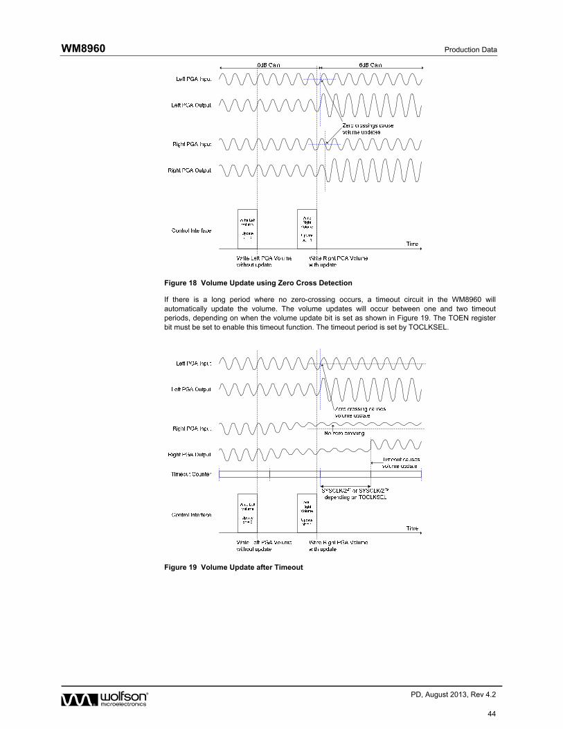
WM8960 Production Data
w PD, August 2013, Rev 4.2
44
Figure 18 Volume Update using Zero Cross Detection
If there is a long period where no zero-crossing occurs, a timeout circuit in the WM8960 will automatically update the volume. The volume updates will occur between one and two timeout periods, depending on when the volume update bit is set as shown in Figure 19. The TOEN register bit must be set to enable this timeout function. The timeout period is set by TOCLKSEL.
Figure 19 Volume Update after Timeout

Production Data WM8960
w PD, August 2013, Rev 4.2
45
HEADPHONE JACK DETECT
The ADCLRC/GPIO1, LINPUT3/JD2 and RINPUT3/JD3 pins can be selected as headphone jack detect inputs to automatically disable the speaker output and enable the headphone output e.g. when a headphone is plugged into a jack socket. In this mode, enabled by setting HPSWEN, the headphone detect input pin switches between headphone and speaker outputs (e.g. when the pin is connected to a mechanical switch in the headphone socket to detect plug-in). The HPSEL[1:0] bits select the input pin used for this function. The HPSWPOL bit reverses the pin’s polarity. Note that the LOUT1, ROUT1, SPKL and SPKR bits in register 26 must also be set for headphone and speaker output (see Table 29 and Table 30).
TOEN must also be set to enable the clock which is used for de-bouncing the jack detect input. TOCLKSEL selects a fast or slow de-bounce period. Note that SYSCLK must be enabled to use this function.
When using capless mode, the OUT3CAP bit should be enabled so that OUT3 is enabled/disabled at the same time as HP_L and HP_R to prevent pop noise.
The debounced headphone detect signal can also be output to the ADCLRC/GPIO1 pin (See GPIO section). This function is not available when using GPIO1 as an input or as ADCLRC.
When using the ADCLRC/GPIO1 pin as a headphone detect input, the ALRCGPIO register bit needs to be set to 1. In this mode, DACLRC is used for both ADC and DAC frame clocks. (See GPIO section for more information)
Note:
When LINPUT3 or RINPUT3 is used as the headphone detect input, the thresholds become CMOS levels (0.3 AVDD / 0.7 AVDD).
HPSWEN HPSWPOL HEADPHONE DETECT PIN
(LINPUT3/JD2, RINPUT3/JD3 OR ADCLRC/GPIO1)
L/ROUT1
(AND OUT3 IN CAPLESS MODE)
(REG. 26)
SPKL/R
(REG. 26)
HEADPHONE ENABLED
(AND OUT3 IN CAPLESS MODE)
SPEAKER ENABLED
0 X X 0 0 no no
0 X X 0 1 no yes
0 X X 1 0 yes no
0 X X 1 1 yes yes
1 0 0 X 0 no no
1 0 0 X 1 no yes
1 0 1 0 X no no
1 0 1 1 X yes no
1 1 0 0 X no no
1 1 0 1 X yes no
1 1 1 X 0 no no
1 1 1 X 1 no yes
Table 29 Headphone Jack Detect Operation
REGISTER ADDRESS
BIT LABEL DEFAULT DESCRIPTION
R24 (18h)
Additional Control (2)
6 HPSWEN 0
Headphone Switch Enable
0 = Headphone switch disabled
1 = Headphone switch enabled
5 HPSWPOL 0 Headphone Switch Polarity
0 = HPDETECT high = headphone
1 = HPDETECT high = speaker
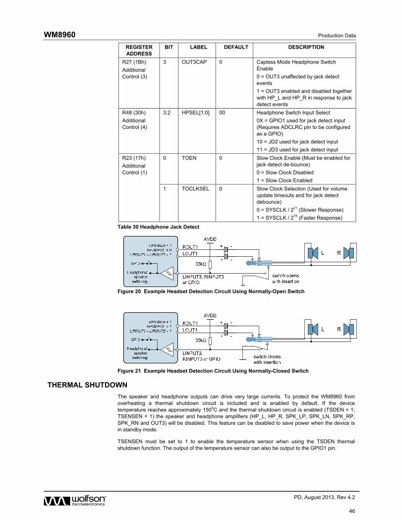
WM8960 Production Data
w PD, August 2013, Rev 4.2
46
REGISTER ADDRESS
BIT LABEL DEFAULT DESCRIPTION
R27 (1Bh)
Additional Control (3)
3 OUT3CAP 0 Capless Mode Headphone Switch Enable
0 = OUT3 unaffected by jack detect events
1 = OUT3 enabled and disabled together with HP_L and HP_R in response to jack detect events
R48 (30h)
Additional Control (4)
3:2 HPSEL[1:0] 00 Headphone Switch Input Select
0X = GPIO1 used for jack detect input (Requires ADCLRC pin to be configured as a GPIO)
10 = JD2 used for jack detect input
11 = JD3 used for jack detect input
R23 (17h)
Additional Control (1)
0 TOEN 0 Slow Clock Enable (Must be enabled for jack detect de-bounce)
0 = Slow Clock Disabled
1 = Slow Clock Enabled
1 TOCLKSEL 0 Slow Clock Selection (Used for volume update timeouts and for jack detect debounce)
0 = SYSCLK / 221 (Slower Response)
1 = SYSCLK / 219 (Faster Response)
Table 30 Headphone Jack Detect
Figure 20 Example Headset Detection Circuit Using Normally-Open Switch
Figure 21 Example Headset Detection Circuit Using Normally-Closed Switch
THERMAL SHUTDOWN
The speaker and headphone outputs can drive very large currents. To protect the WM8960 from overheating a thermal shutdown circuit is included and is enabled by default. If the device temperature reaches approximately 1500C and the thermal shutdown circuit is enabled (TSDEN = 1; TSENSEN = 1) the speaker and headphone amplifiers (HP_L, HP_R, SPK_LP, SPK_LN, SPK_RP, SPK_RN and OUT3) will be disabled. This feature can be disabled to save power when the device is in standby mode.
TSENSEN must be set to 1 to enable the temperature sensor when using the TSDEN thermal shutdown function. The output of the temperature sensor can also be output to the GPIO1 pin.

Production Data WM8960
w PD, August 2013, Rev 4.2
47
REGISTER ADDRESS
BIT LABEL DEFAULT DESCRIPTION
R23 (17h)
Additional Control (1)
8 TSDEN 1 Thermal Shutdown Enable
0 = Thermal shutdown disabled
1 = Thermal shutdown enabled
(TSENSEN must be enabled for this function to work)
R48 (30h)
Additional Control (4)
1 TSENSEN 1 Temperature Sensor Enable
0 = Temperature sensor disabled
1 = Temperature sensor enabled
Table 31 Thermal Shutdown
GENERAL PURPOSE INPUT/OUTPUT The WM8960 has three dual purpose input/output pins.
LINPUT3/JD2: Analogue input or headphone detect input.
RINPUT3/JD3: Analogue input or headphone detect input.
ADCLRC/GPIO1: ADC left/right frame clock or GPIO pin.
The ADCLRC/GPIO1 pin can be configured as a left/right frame clock for the ADC, a headphone detect input, or one of a number of GPIO output functions as shown in Table 32.
The default configuration for the LINPUT3 and RINPUT2 pins is to be analogue inputs. The default configuration for the ADCLRC/GPIO1 pin is to be the ADC left/right frame clock.
REGISTER ADDRESS
BIT LABEL DEFAULT DESCRIPTION
R9 (09h)
Audio Interface (2)
6 ALRCGPIO 0 ADCLRC/GPIO1 Pin Function Select
0 = ADCLRC frame clock for ADC
1 = GPIO pin
R48 (30h)
Additional
Control (4)
6:4 GPIOSEL
[2:0]
000 ADCLRC/GPIO1 GPIO Function Select:
000 = Jack detect input
001 = Reserved
010 = Temperature ok
011 = Debounced jack detect output
100 = SYSCLK output
101 = PLL lock
110 = Logic 0
111 = Logic 1
7 GPIOPOL 0 GPIO Polarity Invert
0 = Non inverted
1 = Inverted
R52 (34h)
Clocking (2)
8:6 OPCLKDIV
[2:0]
000 SYSCLK Output to GPIO Clock Division ratio
000 = SYSCLK
001 = SYSCLK / 2
010 = SYSCLK / 3
011 = SYSCLK / 4
100 = SYSCLK / 5.5
101 = SYSCLK / 6
Table 32 GPIO Control
Slow clock must be enabled (TOEN = 1) when using the jack detect function. This slow clock is used to debounce the jack detect input. The debounce period can be selected using TOCLKSEL.
The temperature sensor must be enabled for the "Temperature ok" GPIO output to function properly.
WM8960 Production Data
w PD, August 2013, Rev 4.2
48
For further details of the Jack detect operation see the Headphone Switch section.
DIGITAL AUDIO INTERFACE
The digital audio interface is used for inputting DAC data into the WM8960 and outputting ADC data from it. It uses five pins:
ADCDAT: ADC data output
ADCLRC: ADC data alignment clock
DACDAT: DAC data input
DACLRC: DAC data alignment clock
BCLK: Bit clock, for synchronisation
The clock signals BCLK, ADCLRC and DACLRC can be outputs when the WM8960 operates as a master, or inputs when it is a slave (see Master and Slave Mode Operation, below).
ADCLRC can also be configured as a GPIO pin. In this case, the ADC will use DACLRC as a frame clock. The ADCLRC/GPIO1 pin function should not be modified while the ADC is enabled.
Four different audio data formats are supported:
Left justified
Right justified
I2S
DSP mode
All four of these modes are MSB first. They are described in Audio Data Formats, below. Refer to the Electrical Characteristic section for timing information.
MASTER AND SLAVE MODE OPERATION
The WM8960 can be configured as either a master or slave mode device. As a master device the WM8960 generates BCLK, ADCLRC and DACLRC and thus controls sequencing of the data transfer on ADCDAT and DACDAT. In slave mode, the WM8960 responds with data to clocks it receives over the digital audio interface. The mode can be selected by writing to the MS bit. Master and slave modes are illustrated below.
Figure 22 Master Mode Figure 23 Slave Mode
OPERATION WITH ADCLRC AS GPIO
When ALRCGPIO=1, the DACLRC pin is used as a frame clock for ADCs and DACs as shown below. The ADCs and DACs must operate at the same sample rate in this mode. See Table 32 for details of GPIO pin configuration.
Figure 24 Master Mode with ADCLRC as GPIO Figure 25 Slave Mode with ADCLRC as GPIO
BCLK
ADCDAT
ADCLRC
DACDAT
DACLRCWM8960CODEC
DSPENCODER/DECODER
Note: The ADC and DAC can run at different sample rates
BCLK
ADCDAT
ADCLRC
DACDAT
DACLRCWM8960CODEC
DSPENCODER/DECODER
Note: The ADC and DAC can run at different sample rates

Production Data WM8960
w PD, August 2013, Rev 4.2
49
BCLK DIVIDE
The BCLK frequency in master mode is controlled by BCLKDIV[3:0]. When the ADCs and DACs are operating at different sample rates, BCLKDIV must be set appropriately to support the data rate of whichever is the faster.
Internal clock divide and phase control mechanisms ensure that the BCLK, ADCLRC and DACLRC edges will occur in a predictable and repeatable position relative to each other and to the data for a given combination of DAC sample rate, ADC sample rate and BCLKDIV settings.
See Clocking and Sample Rates section for more information.
AUDIO DATA FORMATS
In Left Justified mode, the MSB is available on the first rising edge of BCLK following a LRCLK transition. The other bits up to the LSB are then transmitted in order. Depending on word length, BCLK frequency and sample rate, there may be unused BCLK cycles before each LRCLK transition.
Figure 26 Left Justified Audio Interface (assuming n-bit word length)
In Right Justified mode, the LSB is available on the last rising edge of BCLK before a LRCLK transition. All other bits are transmitted before (MSB first). Depending on word length, BCLK frequency and sample rate, there may be unused BCLK cycles after each LRCLK transition.
Figure 27 Right Justified Audio Interface (assuming n-bit word length)
In I2S mode, the MSB is available on the second rising edge of BCLK following a LRCLK transition. The other bits up to the LSB are then transmitted in order. Depending on word length, BCLK frequency and sample rate, there may be unused BCLK cycles between the LSB of one sample and the MSB of the next.
WM8960 Production Data
w PD, August 2013, Rev 4.2
50
Figure 28 I2S Justified Audio Interface (assuming n-bit word length)
In DSP/PCM mode, the left channel MSB is available on either the 1st (mode B) or 2nd (mode A) rising edge of BCLK (selectable by LRP) following a rising edge of LRC. Right channel data immediately follows left channel data. Depending on word length, BCLK frequency and sample rate, there may be unused BCLK cycles between the LSB of the right channel data and the next sample.
In device master mode, the LRC output will resemble the frame pulse shown in Figure 29 and Figure 30. In device slave mode, Figure 31 and Figure 32, it is possible to use any length of frame pulse less than 1/fs, providing the falling edge of the frame pulse occurs greater than one BCLK period before the rising edge of the next frame pulse.
Figure 29 DSP/PCM Mode Audio Interface (mode A, LRP=0, Master)
Figure 30 DSP/PCM Mode Audio Interface (mode B, LRP=1, Master)

Production Data WM8960
w PD, August 2013, Rev 4.2
51
Figure 31 DSP/PCM Mode Audio Interface (mode A, LRP=0, Slave)
Figure 32 DSP/PCM Mode Audio Interface (mode B, LRP=1, Slave)
WM8960 Production Data
w PD, August 2013, Rev 4.2
52
AUDIO INTERFACE CONTROL
The register bits controlling audio format, word length and master / slave mode are summarised in Table 33. MS selects audio interface operation in master or slave mode. In Master mode BCLK, ADCLRC and DACLRC are outputs. The frequency of ADCLRC and DACLRC is set by the bits ADCDIV and DACDIV and the frequency of BCLK is set by the bits BCLKDIV (See "Clocking and Sample Rates"). In Slave mode BCLK, ADCLRC and DACLRC are inputs.
REGISTER ADDRESS
BIT LABEL DEFAULT DESCRIPTION
R7 (07h)
Digital Audio Interface Format
8 ALRSWAP 0 Left/Right ADC channel swap
1 = Swap left and right ADC data in audio interface
0 = Output left and right data as normal
7 BCLKINV 0 BCLK invert bit (for master and slave modes)
0 = BCLK not inverted
1 = BCLK inverted
6 MS 0 Master / Slave Mode Control
0 = Enable slave mode
1 = Enable master mode
5 DLRSWAP 0 Left/Right DAC Channel Swap
0 = Output left and right data as normal
1 = Swap left and right DAC data in audio interface
4 LRP 0 Right, left and I2S modes – LRCLK polarity
0 = normal LRCLK polarity
1 = invert LRCLK polarity
DSP Mode – mode A/B select
0 = MSB is available on 2nd BCLK rising edge after LRC rising edge (mode A)
1 = MSB is available on 1st BCLK rising edge after LRC rising edge (mode B)
3:2 WL[1:0] 10 Audio Data Word Length
00 = 16 bits
01 = 20 bits
10 = 24 bits
11 = 32 bits (see Note)
1:0 FORMAT[1:0] 10 Audio Data Format Select
00 = Right justified
01 = Left justified
10 = I2S Format
11 = DSP Mode
Table 33 Audio Data Format Control
Note: Right Justified mode does not support 32-bit data.
Production Data WM8960
w PD, August 2013, Rev 4.2
53
AUDIO INTERFACE OUTPUT TRISTATE
Register bit TRIS, register 24(18h) bit[3] can be used to tristate the ADCDAT pin and switch ADCLRC, DACLRC and BCLK to inputs. In Slave mode (MS=0) ADCLRC, DACLRC and BCLK are by default configured as inputs and only ADCDAT will be tri-stated, (see Table 34).
When the ADCLRC/GPIO1 pin is configured as a GPIO, this pin will not be tristated by the TRIS register bit.
REGISTER ADDRESS
BIT LABEL
DEFAULT DESCRIPTION
R24 (18h) Additional Control (2)
3 TRIS 0 Tristates ADCDAT and switches ADCLRC, DACLRC and BCLK to inputs.
0 = ADCDAT is an output; ADCLRC, DACLRC and BCLK are inputs (slave mode) or outputs (master mode)
1 = ADCDAT is tristated; DACLRC and BCLK are inputs; ADCLRC is an input (when not configured as a GPIO)
Table 34 Tri-stating the Audio Interface
MASTER MODE ADCLRC AND DACLRC ENABLE
In master mode, by default ADCLRC clock generator is disabled and will output a logic 0 when the ADCs are both disabled and DACLRC clock generator is disabled and will output a logic 0 when the DACs are both disabled.
Register bit LRCM, register 24 (18h) bit[2] changes the control so that the ADCLRC and DACLRC clock generators are both disabled only when both ADCs and both DACs are disabled. This enables the user to use e.g. ADCLRC for both ADC and DAC LRCLK and disable the ADC when DAC only operation is required, (see Table 35).
When ADCLRC is configured as a GPIO (using ALRCGPIO), DACLRC is used for the ADCs and the DACs and will only be disabled in master mode when both ADCs and both DACs are disabled.
Figure 33 Master Mode Clock Output Control
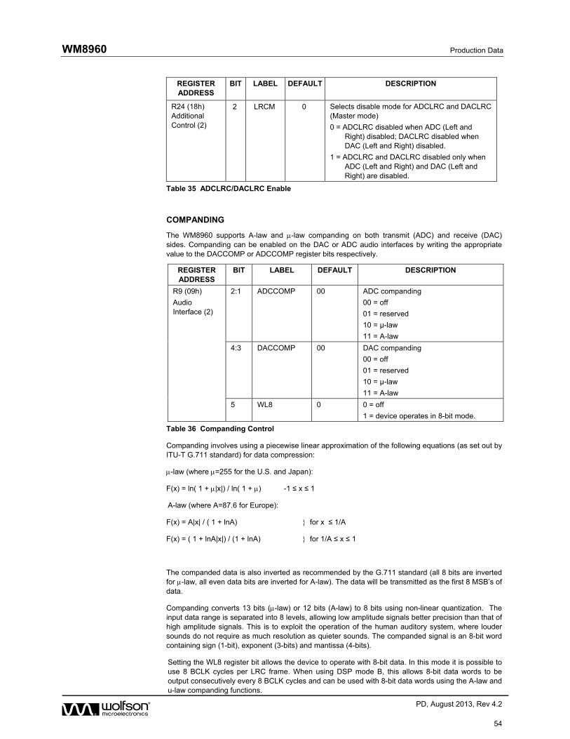
WM8960 Production Data
w PD, August 2013, Rev 4.2
54
REGISTER ADDRESS
BIT LABEL
DEFAULT DESCRIPTION
R24 (18h) Additional Control (2)
2 LRCM 0 Selects disable mode for ADCLRC and DACLRC (Master mode)
0 = ADCLRC disabled when ADC (Left and Right) disabled; DACLRC disabled when DAC (Left and Right) disabled.
1 = ADCLRC and DACLRC disabled only when ADC (Left and Right) and DAC (Left and Right) are disabled.
Table 35 ADCLRC/DACLRC Enable
COMPANDING
The WM8960 supports A-law and -law companding on both transmit (ADC) and receive (DAC) sides. Companding can be enabled on the DAC or ADC audio interfaces by writing the appropriate value to the DACCOMP or ADCCOMP register bits respectively.
REGISTER ADDRESS
BIT LABEL DEFAULT DESCRIPTION
R9 (09h)
Audio Interface (2)
2:1 ADCCOMP 00 ADC companding
00 = off
01 = reserved
10 = µ-law
11 = A-law
4:3 DACCOMP 00 DAC companding
00 = off
01 = reserved
10 = µ-law
11 = A-law
5 WL8 0 0 = off
1 = device operates in 8-bit mode.
Table 36 Companding Control
Companding involves using a piecewise linear approximation of the following equations (as set out by ITU-T G.711 standard) for data compression:
-law (where =255 for the U.S. and Japan):
F(x) = ln( 1 + |x|) / ln( 1 + ) -1 ≤ x ≤ 1
A-law (where A=87.6 for Europe):
F(x) = A|x| / ( 1 + lnA) for x ≤ 1/A
F(x) = ( 1 + lnA|x|) / (1 + lnA) for 1/A ≤ x ≤ 1
The companded data is also inverted as recommended by the G.711 standard (all 8 bits are inverted for -law, all even data bits are inverted for A-law). The data will be transmitted as the first 8 MSB’s of data.
Companding converts 13 bits (-law) or 12 bits (A-law) to 8 bits using non-linear quantization. The input data range is separated into 8 levels, allowing low amplitude signals better precision than that of high amplitude signals. This is to exploit the operation of the human auditory system, where louder sounds do not require as much resolution as quieter sounds. The companded signal is an 8-bit word containing sign (1-bit), exponent (3-bits) and mantissa (4-bits).
Setting the WL8 register bit allows the device to operate with 8-bit data. In this mode it is possible to use 8 BCLK cycles per LRC frame. When using DSP mode B, this allows 8-bit data words to be output consecutively every 8 BCLK cycles and can be used with 8-bit data words using the A-law and u-law companding functions.

Production Data WM8960
w PD, August 2013, Rev 4.2
55
BIT7 BIT[6:4] BIT[3:0]
SIGN EXPONENT MANTISSA
Table 37 8-bit Companded Word Composition
u-law Companding
0
20
40
60
80
100
120
0 0.1 0.2 0.3 0.4 0.5 0.6 0.7 0.8 0.9 1
Normalised Input
Co
mp
and
ed O
utp
ut
0
0.1
0.2
0.3
0.4
0.5
0.6
0.7
0.8
0.9
1
No
rmal
ised
Ou
tpu
t
Figure 34 µ-Law Companding
A-law Companding
0
20
40
60
80
100
120
0 0.2 0.4 0.6 0.8 1
Normalised Input
Co
mp
and
ed O
utp
ut
0
0.1
0.2
0.3
0.4
0.5
0.6
0.7
0.8
0.9
1
No
rmal
ised
Ou
tpu
t
Figure 35 A-Law Companding
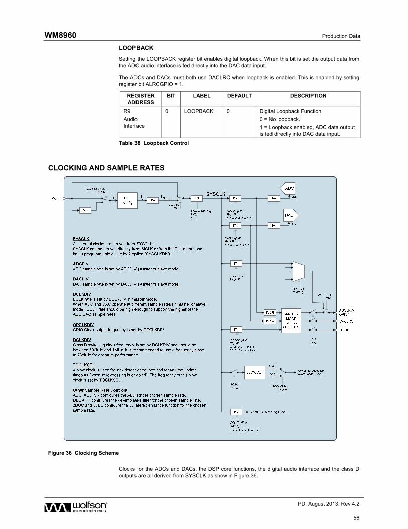
WM8960 Production Data
w PD, August 2013, Rev 4.2
56
LOOPBACK
Setting the LOOPBACK register bit enables digital loopback. When this bit is set the output data from the ADC audio interface is fed directly into the DAC data input.
The ADCs and DACs must both use DACLRC when loopback is enabled. This is enabled by setting register bit ALRCGPIO = 1.
REGISTER ADDRESS
BIT LABEL DEFAULT DESCRIPTION
R9
Audio Interface
0 LOOPBACK 0 Digital Loopback Function
0 = No loopback.
1 = Loopback enabled, ADC data output is fed directly into DAC data input.
Table 38 Loopback Control
CLOCKING AND SAMPLE RATES
Figure 36 Clocking Scheme
Clocks for the ADCs and DACs, the DSP core functions, the digital audio interface and the class D outputs are all derived from SYSCLK as show in Figure 36.
Production Data WM8960
w PD, August 2013, Rev 4.2
57
SYSCLK can either be derived directly from MCLK, or generated from a PLL using MCLK as a reference. The clock source is selected by CLKSEL. Many commonly-used audio sample rates can be derived directly from MCLK, while the PLL provides additional flexibility.
The ADC and DAC sample rates are independently selectable, relative to SYSCLK, using ADCDIV and DACDIV. In master mode, BCLK is also derived from SYSCLK via a programmable clock divide (BCLKDIV).
When the ADCLRC/GPIO1 pin is configured as a GPIO, a clock derived from SYSCLK can be output on this pin to provide clocking for other parts of the system. The frequency of this output clock is set by OPCLKDIV.
A slow clock derived from SYSCLK is used to de-bounce the headphone detect function, and to set the timeout period for volume updates when zero-cross functions are used. This clock is enabled by TOEN and its frequency is set by TOCLKSEL.
The class D outputs require a clock, and this is also derived from SYSCLK via a programmable divider (DCLKDIV) as shown in Figure 36. The class D switching clock should be set between 700kHz and 800kHz.
The class D switching clock should not be disabled when the speaker outputs are active, as this would prevent the speaker outputs from functioning. The class D switching clock frequency should not be altered while the speaker outputs are active as this may generate an audible click.
Table 39 shows the clocking and sample rate controls for MCLK input, BITCLK output (in master mode), ADCs, DACs, class D outputs and GPIO clock output. Refer to Table 40 for example clocking configurations.
REGISTER ADDRESS
BIT LABEL DEFAULT DESCRIPTION
R4 (04h)
Clocking (1)
8:6 ADCDIV
[2:0]
000 ADC Sample rate divider (Also determines ADCLRC in master mode)
000 = SYSCLK / (1.0 * 256)
001 = SYSCLK / (1.5 * 256)
010 = SYSCLK / (2 * 256)
011 = SYSCLK / (3 * 256)
100 = SYSCLK / (4 * 256)
101 = SYSCLK / (5.5 * 256)
110 = SYSCLK / (6 * 256)
111 = Reserved
5:3 DACDIV
[2:0]
000 DAC Sample rate divider (Also determines DACLRC in master mode)
000 = SYSCLK / (1.0 * 256)
001 = SYSCLK / (1.5 * 256)
010 = SYSCLK / (2 * 256)
011 = SYSCLK / (3 * 256)
100 = SYSCLK / (4 * 256)
101 = SYSCLK / (5.5 * 256)
110 = SYSCLK / (6 * 256)
111 = Reserved
2:1 SYSCLKDIV
[1:0]
00 SYSCLK Pre-divider. Clock source (MCLK or PLL output) will be divided by this value to generate SYSCLK.
00 = Divide SYSCLK by 1
01 = Reserved
10 = Divide SYSCLK by 2
11 = Reserved
0 CLKSEL 0 SYSCLK selection
0 = SYSCLK derived from MCLK
1 = SYSCLK derived from PLL output
WM8960 Production Data
w PD, August 2013, Rev 4.2
58
REGISTER ADDRESS
BIT LABEL DEFAULT DESCRIPTION
R8 (08h)
Clocking (2)
8:6 DCLKDIV 111 Class D switching clock divider. 000 = SYSCLK / 1.5 001 = SYSCLK / 2 010 = SYSCLK / 3 011 = SYSCLK / 4 100 = SYSCLK / 6 101 = SYSCLK / 8 110 = SYSCLK / 12 111 = SYSCLK / 16
3:0 BCLKDIV[3:0] 0000 BCLK Frequency (Master Mode) 0000 = SYSCLK 0001 = SYSCLK / 1.5 0010 = SYSCLK / 2 0011 = SYSCLK / 3 0100 = SYSCLK / 4 0101 = SYSCLK / 5.5 0110 = SYSCLK / 6 0111 = SYSCLK / 8 1000 = SYSCLK / 11 1001 = SYSCLK / 12 1010 = SYSCLK / 16 1011 = SYSCLK / 22 1100 = SYSCLK / 24 1101 to 1111 = SYSCLK / 32
Table 39 ADC, DAC and BCLK Control
SYSCLK
(=MCLK OR PLL OUTPUT)
(MHz)
ADCDIV OR DACDIV
ADC / DAC SAMPLE RATE (kHz)
12.288
000 (=1) 48
001 (=1.5) 32
010 (=2) 24
011 (=3) 16
100 (=4) 12
101 (=5.5) (Not used)
110 (=6) 8
111 Reserved
11.2896
000 (=1) 44.1
001 (=1.5) (Not used)
010 (=2) 22.05
011 (=3) (Not used)
100 (=4) 11.025
101 (=5.5) 8.018
110 (=6) (Not used)
111 Reserved
2.048
000 (=1) 8
001 (=1.5) (Not used)
010 (=2) (Not used)
011 (=3) (Not used)
100 (=4) (Not used)
101 (=5.5) (Not used)
110 (=6) (Not used)
111 Reserved
Table 40 ADC and DAC Sample Rates

Production Data WM8960
w PD, August 2013, Rev 4.2
59
Although the ADC and DAC can run at different sample rates, they share the same bit clock pin BCLK.
When operating in master mode, register bits BCLKDIV[3:0] should be set to an appropriate value to ensure that there are sufficient BCLK cycles to transfer the complete data word from the ADCs and to the DACs.
When operating in slave mode, the host device must provide sufficient BCLK cycles to transfer complete data words to the ADCs and DACs.
Table 41 shows the maximum word lengths supported for a given SYSCLK and BCLKDIV, assuming that either the ADCs or DACs are running at maximum rate (i.e. ADCDIV[2:0]=000 or DACDIV[2:0]=000).
SYSCLK
(=MCLK OR PLL OUTPUT)
(MHz)
BCLKDIV[3:0] BCLK RATE (MASTER MODE)
(MHz)
MAXIMUM WORD LENGTH (AT MAXIMUM ADC OR DAC SAMPLE RATE)
12.288
0000 (=1) 12.288 32
0001 (=1.5) 8.192 32
0010 (=2) 6.144 32
0011 (=3) 4.096 32
0100 (=4) 3.072 32
0101 (=5.5) 2.2341818 20
0110 (=6) 2.048 20
0111 (=8) 1.536 16
1000 (=11) 1.117091 8
1001 (=12) 1.024 8
1010 (=16) 0.768 8
1011 (=22) 0.558545 N/A
1100 (=24) 0.512 N/A
1101 (=32) 0.384 N/A
1110 (=32) 0.384 N/A
1111 (=32) 0.384 N/A
11.2896
0000 (=1) 11.2896 32
0001 (=1.5) 7.5264 32
0010 (=2) 5.6448 32
0011 (=3) 3.7632 32
0100 (=4) 2.8224 32
0101 (=5.5) 2.052655 20
0110 (=6) 1.8816 20
0111 (=8) 1.4112 16
1000 (=11) 1.026327 8
1001 (=12) 0.9408 8
1010 (=16) 0.7056 8
1011 (=22) 0.513164 N/A
1100 (=24) 0.4704 N/A
1101 (=32) 0.3528 N/A
1110 (=32) 0.3528 N/A
1111 (=32) 0.3528 N/A
Table 41 BCLK Divider in Master Mode
OTHER SAMPLE RATE CONTROL BITS
The ALC, de-emphasis filter and 3D stereo enhance functions all need to be configured for the chosen sample rate when in use, as show in Table 42.
ADC_ALC_SR should be configured to match the chosen ADC sample rate.
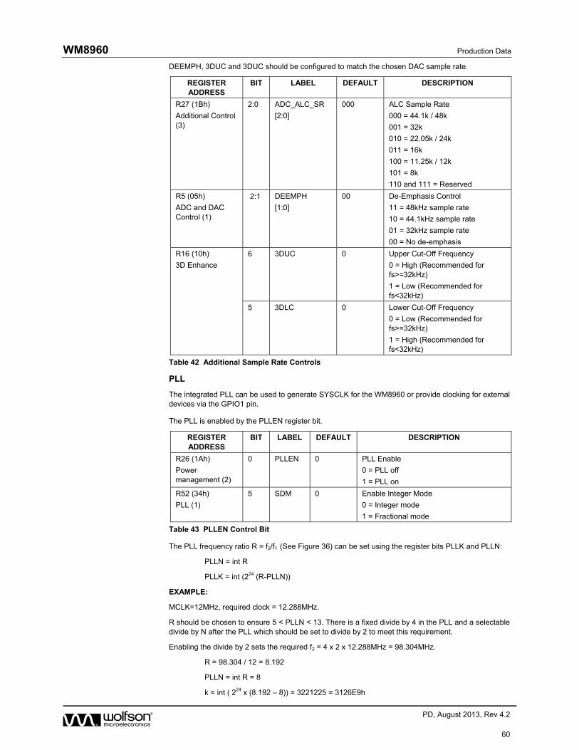
WM8960 Production Data
w PD, August 2013, Rev 4.2
60
DEEMPH, 3DUC and 3DUC should be configured to match the chosen DAC sample rate.
REGISTER ADDRESS
BIT LABEL DEFAULT DESCRIPTION
R27 (1Bh)
Additional Control (3)
2:0 ADC_ALC_SR
[2:0]
000 ALC Sample Rate
000 = 44.1k / 48k
001 = 32k
010 = 22.05k / 24k
011 = 16k
100 = 11.25k / 12k
101 = 8k
110 and 111 = Reserved
R5 (05h)
ADC and DAC Control (1)
2:1 DEEMPH
[1:0]
00 De-Emphasis Control
11 = 48kHz sample rate
10 = 44.1kHz sample rate
01 = 32kHz sample rate
00 = No de-emphasis
R16 (10h)
3D Enhance
6 3DUC 0 Upper Cut-Off Frequency
0 = High (Recommended for fs>=32kHz)
1 = Low (Recommended for fs<32kHz)
5 3DLC 0 Lower Cut-Off Frequency
0 = Low (Recommended for fs>=32kHz)
1 = High (Recommended for fs<32kHz)
Table 42 Additional Sample Rate Controls
PLL
The integrated PLL can be used to generate SYSCLK for the WM8960 or provide clocking for external devices via the GPIO1 pin.
The PLL is enabled by the PLLEN register bit.
REGISTER ADDRESS
BIT LABEL DEFAULT DESCRIPTION
R26 (1Ah)
Power management (2)
0 PLLEN 0 PLL Enable
0 = PLL off
1 = PLL on
R52 (34h)
PLL (1)
5 SDM 0 Enable Integer Mode
0 = Integer mode
1 = Fractional mode
Table 43 PLLEN Control Bit
The PLL frequency ratio R = f2/f1 (See Figure 36) can be set using the register bits PLLK and PLLN:
PLLN = int R
PLLK = int (224 (R-PLLN))
EXAMPLE:
MCLK=12MHz, required clock = 12.288MHz.
R should be chosen to ensure 5 < PLLN < 13. There is a fixed divide by 4 in the PLL and a selectable divide by N after the PLL which should be set to divide by 2 to meet this requirement.
Enabling the divide by 2 sets the required f2 = 4 x 2 x 12.288MHz = 98.304MHz.
R = 98.304 / 12 = 8.192
PLLN = int R = 8
k = int ( 224 x (8.192 – 8)) = 3221225 = 3126E9h

Production Data WM8960
w PD, August 2013, Rev 4.2
61
REGISTER ADDRESS
BIT LABEL DEFAULT DESCRIPTION
R52 (34h)
PLL N value
4 PLLPRESCALE 0 Divide MCLK by 2 before input to PLL
0 = Divide by 1
1 = Divide by 2
3:0 PLLN 8h Integer (N) part of PLL input/output frequency ratio. Use values greater than 5 and less than 13.
R53 (35h)
PLL K value (1)
5:0 PLLK [23:16] 31h Fractional (K) part of PLL1 input/output frequency ratio (treat as one 24-digit binary number).
R54 (36h)
PLL K Value (2)
8:0 PLLK [15:8] 26h
R55 (37h)
PLL K Value (3)
8:0 PLLK [7:0] E9h
Table 44 PLL Frequency Ratio Control
The PLL performs best when f2 is between 90MHz and 100MHz. Its stability peaks at N=8. Some example settings are shown in Table 45.
MCLK
(MHz)
(f1)
DESIRED OUTPUT (SYSCLK)
(MHz)
f2
(MHz)
PR
ES
CA
LE
DIV
IDE
(PL
LP
RE
SC
AL
E)
PO
ST
SC
AL
E D
IVID
E
(SY
SC
LK
DIV
[1:0
])
FIX
ED
PO
ST
-DIV
IDE
R N K
12 11.2896 90.3168 1 2 4 7.5264 7h 86C226h
12 12.288 98.304 1 2 4 8.192 8h 3126E8h
13 11.2896 90.3168 1 2 4 6.947446 6h F28BD4h
13 12.288 98.304 1 2 4 7.561846 7h 8FD525h
14.4 11.2896 90.3168 1 2 4 6.272 6h 45A1CAh
14.4 12.288 98.304 1 2 4 6.826667 6h D3A06Eh
19.2 11.2896 90.3168 2 2 4 9.408 9h 6872AFh
19.2 12.288 98.304 2 2 4 10.24 Ah 3D70A3h
19.68 11.2896 90.3168 2 2 4 9.178537 9h 2DB492h
19.68 12.288 98.304 2 2 4 9.990243 9h FD809Fh
19.8 11.2896 90.3168 2 2 4 9.122909 9h 1F76F7h
19.8 12.288 98.304 2 2 4 9.929697 9h EE009Eh
24 11.2896 90.3168 2 2 4 7.5264 7h 86C226h
24 12.288 98.304 2 2 4 8.192 8h 3126E8h
26 11.2896 90.3168 2 2 4 6.947446 6h F28BD4h
26 12.288 98.304 2 2 4 7.561846 7h 8FD525h
27 11.2896 90.3168 2 2 4 6.690133 6h B0AC93h
27 12.288 98.304 2 2 4 7.281778 7h 482296h
Table 45 PLL Frequency Examples

WM8960 Production Data
w PD, August 2013, Rev 4.2
62
Device running in master mode with 24-bit data
MCLK input at 12.288MHz
ADC and DAC running at fs=48kHz
BCLK running at 64fs
Device running in slave mode with 24-bit data
MCLK input at 12.288MHz
ADC and DAC running at fs=48kHz
BCLK supplied from host at 64fs in this example
Device running in master mode with 24-bit data
MCLK input at 11.2896MHz
ADC running at fs=8.018kHz
DAC running at fs=44.1kHz
BCLK running at 64fs (relative to DAC sample rate, as DAC is operating at a higher sample rate than ADC)
Device running in slave mode with 24-bit data
MCLK input at 11.2896MHz
ADC running at fs=8.018kHz
DAC running at fs=44.1kHz
BCLK supplied from host at 64fs in this example (relative to DAC sample rate, as DAC is operating at a higher sample rate than ADC)
Device running in master mode with 24-bit data
MCLK input at 12MHz
PLL Enabled and configured for SYSCLK=11.2896MHz
ADC running at fs=8.018kHz
DAC running at fs=44.1kHz
BCLK running at 64fs (relative to DAC sample rate, as DAC is operating at a higher sample rate than ADC)
Class D clocks running at 705.6kHz
Table 46 Example Clocking Schemes

Production Data WM8960
w PD, August 2013, Rev 4.2
63
CONTROL INTERFACE
2-WIRE SERIAL CONTROL INTERFACE
The WM8960 is controlled by writing to registers through a 2-wire serial control interface. A control word consists of 16 bits. The first 7 bits (B15 to B9) are address bits that select which control register is accessed. The remaining 9 bits (B8 to B0) are data bits, corresponding to the 9 bits in each control register. Many devices can be controlled by the same bus, and each device has a unique 7-bit address (this is not the same as the 7-bit address of each register in the WM8960).
The device address is 0011010 (0x34h).
The WM8960 operates as a slave device only. The controller indicates the start of data transfer with a high to low transition on SDIN while SCLK remains high. This indicates that a device address and data will follow. All devices on the 2-wire bus respond to the start condition and shift in the next eight bits on SDIN (7-bit address + Read/Write bit, MSB first). If the device address received matches the address of the WM8960 and the R/W bit is ‘0’, indicating a write, then the WM8960 responds by pulling SDIN low on the next clock pulse (ACK). If the address is not recognised or the R/W bit is ‘1’, the WM8960 returns to the idle condition and wait for a new start condition and valid address.
Once the WM8960 has acknowledged a correct address, the controller sends the first byte of control data (B15 to B8, i.e. the WM8960 register address plus the first bit of register data). The WM8960 then acknowledges the first data byte by pulling SDIN low for one clock pulse. The controller then sends the second byte of control data (B7 to B0, i.e. the remaining 8 bits of register data), and the WM8960 acknowledges again by pulling SDIN low.
The transfer of data is complete when there is a low to high transition on SDIN while SCLK is high. After receiving a complete address and data sequence the WM8960 returns to the idle state and waits for another start condition. If a start or stop condition is detected out of sequence at any point during data transfer (i.e. SDIN changes while SCLK is high), the device jumps to the idle condition.
SDIN
SCLK
register address and1st register data bit
DEVICE ADDRESS(7 BITS)
RD / WRBIT
ACK(LOW)
CONTROL BYTE 1(BITS 15 TO 8)
CONTROL BYTE 2(BITS 7 TO 0)
remaining 8 bits ofregister data
STOPSTART
ACK(LOW)
ACK(LOW)
Figure 37 2-Wire Serial Control Interface
POWER MANAGEMENT
The WM8960 has three control registers that allow users to select which functions are active. For minimum power consumption, unused functions should be disabled. To avoid any pop or click noise, it is important to enable or disable functions in the correct order (see Applications Information). VMIDSEL is the enable for the Vmid reference, which defaults to disabled and can be enabled as a 2x50k potential divider or, for low power maintenance of Vref when all other blocks are disabled, as a 2x250k potential divider.
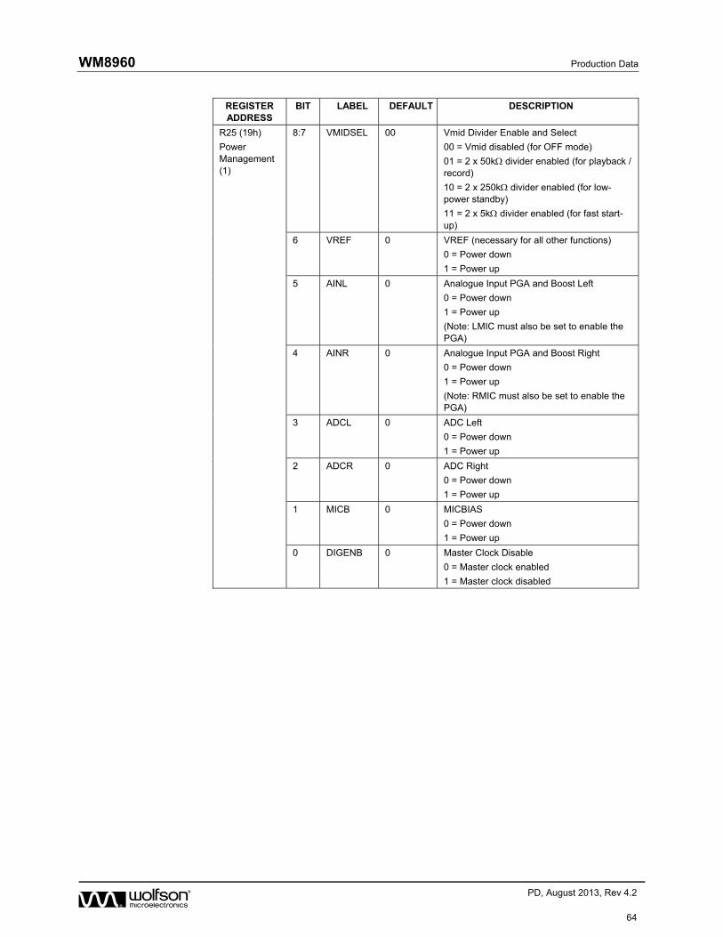
WM8960 Production Data
w PD, August 2013, Rev 4.2
64
REGISTER ADDRESS
BIT LABEL DEFAULT DESCRIPTION
R25 (19h)
Power Management (1)
8:7 VMIDSEL 00 Vmid Divider Enable and Select
00 = Vmid disabled (for OFF mode)
01 = 2 x 50k divider enabled (for playback / record)
10 = 2 x 250k divider enabled (for low-power standby)
11 = 2 x 5k divider enabled (for fast start-up)
6 VREF 0 VREF (necessary for all other functions)
0 = Power down
1 = Power up
5 AINL 0 Analogue Input PGA and Boost Left
0 = Power down
1 = Power up
(Note: LMIC must also be set to enable the PGA)
4 AINR 0 Analogue Input PGA and Boost Right
0 = Power down
1 = Power up
(Note: RMIC must also be set to enable the PGA)
3 ADCL 0 ADC Left
0 = Power down
1 = Power up
2 ADCR 0 ADC Right
0 = Power down
1 = Power up
1 MICB 0 MICBIAS
0 = Power down
1 = Power up
0 DIGENB 0 Master Clock Disable
0 = Master clock enabled
1 = Master clock disabled

Production Data WM8960
w PD, August 2013, Rev 4.2
65
REGISTER ADDRESS
BIT LABEL DEFAULT DESCRIPTION
R26 (1Ah)
Power Management (2)
8 DACL 0 DAC Left
0 = Power down
1 = Power up
7 DACR 0 DAC Right
0 = Power down
1 = Power up
6 LOUT1 0 LOUT1 Output Buffer
0 = Power down
1 = Power up
5 ROUT1 0 ROUT1 Output Buffer
0 = Power down
1 = Power up
4 SPKL 0 SPK_LP/SPK_LN Output PGA.
0 = Power down
1 = Power up
(Note: Speaker output also requires SPK_OP_EN[0] to be set)
3 SPKR 0 SPK_RP/SPK_RN Output PGA
0 = Power down
1 = Power up
(Note: Speaker output also requires SPK_OP_EN[1] to be set)
1 OUT3 0 OUT3 Output Buffer
0 = Power down
1 = Power up
0 PLL_EN 0 PLL Enable
0 = Power down
1 = Power up
R47 (2Fh)
Power Management (3)
5 LMIC Left Input PGA Enable
0 = Power down
1 = Power up
(Note: PGA also requires AINL to be set)
4 RMIC RIght Input PGA Enable
0 = Power down
1 = Power up
(Note: PGA also requires AINR to be set)
3 LOMIX Left Output Mixer Enable
0 = Power down
1 = Power up
2 ROMIX Right Output Mixer Enable
0 = Power down
1 = Power up
Table 47 Power Management
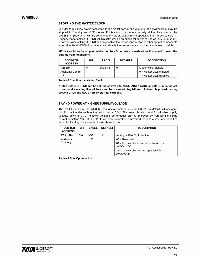
WM8960 Production Data
w PD, August 2013, Rev 4.2
66
STOPPING THE MASTER CLOCK
In order to minimise power consumed in the digital core of the WM8960, the master clock may be stopped in Standby and OFF modes. If this cannot be done externally at the clock source, the DIGENB bit (R25, bit 0) can be set to stop the MCLK signal from propagating into the device core. In Standby mode, setting DIGENB will typically provide an additional power saving on DCVDD of 20uA. However, since setting DIGENB has no effect on the power consumption of other system components external to the WM8960, it is preferable to disable the master clock at its source wherever possible.
MCLK should not be stopped while the class D outputs are enabled, as this would prevent the outputs from functioning.
REGISTER ADDRESS
BIT LABEL DEFAULT DESCRIPTION
R25 (19h)
Additional Control (1)
0 DIGENB 0 Master clock disable
0 = Master clock enabled
1 = Master clock disabled
Table 48 Enabling the Master Clock
NOTE: Before DIGENB can be set, the control bits ADCL, ADCR, DACL and DACR must be set to zero and a waiting time of 1ms must be observed. Any failure to follow this procedure may prevent DACs and ADCs from re-starting correctly.
SAVING POWER AT HIGHER SUPPLY VOLTAGE
The AVDD supply of the WM8960 can operate beteen 2.7V and 3.6V. By default, all analogue circuitry on the device is optimized to run at 3.3V. This set-up is also good for all other supply voltages down to 2.7V. At lower voltages, performance can be improved by increasing the bias current by setting VSEL[1:0] = 01. If low power operation is preferred the bias current can be left at the default setting. This is controlled as shown below.
REGISTER ADDRESS
BIT LABEL DEFAULT DESCRIPTION
R23 (17h)
Additional Control (1)
7:6 VSEL [1:0]
11 Analogue Bias Optimisation
00 = Reserved
01 = Increased bias current optimized for AVDD=2.7V
1X = Lowest bias current, optimized for AVDD=3.3V
Table 49 Bias Optimisation

Production Data WM8960
w PD, August 2013, Rev 4.2
67
REGISTER MAP
REGISTER remarks Bit[8] Bit[7] Bit[6] Bit[5] Bit[4] Bit[3] Bit[2] Bit[1] Bit[0] default
R0 (00h) Left Input volume IPVU LINMUTE LIZC 0_1001_0111
R1 (01h) Right Input volume IPVU RINMUTE RIZC 0_1001_0111
R2 (02h) LOUT1 volume OUT1VU LO1ZC 0_0000_0000
R3 (03h) ROUT1 volume OUT1VU RO1ZC 0_0000_0000
R4 (04h) Clocking (1) CLKSEL 0_0000_0000
R5 (05h) ADC & DAC Control (CTR1) 0 DACDIV2 0 DACMU ADCHPD 0_0000_1000
R6 (06h) ADC & DAC Control (CTR2) 0 0 0 DACSMM DACMR DACSLOPE 0 0_0000_0000
R7 (07h) Audio Interface ALRSWAP BCLKINV MS DLRSWAP LRP 0_0000_1010
R8 (08h) Clocking (2) 0 0 1_1100_0000
R9 (09h) Audio Interface 0 0 ALRCGPIO WL8 LOOPBACK 0_0000_0000
R10 (0Ah) Left DAC volume DACVU 0_1111_1111
R11 (0Bh) Right DAC volume DACVU 0_1111_1111
R12 (0Ch) Reserved 0 0 0 0 0 0 0 0 0 0_0000_0000
R13 (0Dh) Reserved 0 0 0 0 0 0 0 0 0 0_0000_0000
R14 (0Eh) Reserved 0 0 0 0 0 0 0 0 0 0_0000_0000
R15 (0Fh) Reset not reset
R16 (10h) 3D control 0 0 3DUC 3DLC 3DEN 0_0000_0000
R17 (11h) ALC1 0_0111_1011
R18 (12h) ALC2 1 0 1_0000_0000
R19 (13h) ALC3 ALCMODE 0_0011_0010
R20 (14h) Noise Gate 0 0 0 NGAT 0_0000_0000
R21 (15h) Left ADC volume ADCVU 0_1100_0011
R22 (16h) Right ADC volume ADCVU 0_1100_0011
R23 (17h) Additional control(1) TSDEN 0 DMONOMIX TOCLKSEL TOEN 1_1100_0000
R24 (18h) Additional control(2) 0 0 HPSWEN HPSWPOL 0 TRIS LRCM 0 0 0_0000_0000
R25 (19h) Pwr Mgmt (1) VREF AINL AINR ADCL ADCR MICB DIGENB 0_0000_0000
R26 (1Ah) Pwr Mgmt (2) DACL DACR LOUT1 ROUT1 SPKL SPKR 0 OUT3 PLL_EN 0_0000_0000
R27 (1Bh) Additional Control (3) 0 0 VROI 0 0 OUT3CAP 0_0000_0000
R28 (1Ch) Anti-pop 1 0 POBCTRL 0 0 BUFDCOPEN BUFIOEN SOFT_ST 0 HPSTBY 0_0000_0000
R29 (1Dh) Anti-pop 2 0 0 DISOP 0 0 0 0 0_0000_0000
R30 (1Eh) Reserved 0 0 0 0 0 0 0 0 0 0_0000_0000
R31 (1Fh) Reserved 0 0 0 0 0 0 0 0 0 0_0000_0000
R32 (20h) ADCL signal path LMN1 LMP3 LMP2 LMIC2B 0 0 0 1_0000_0000
R33 (21h) ADCR signal path RMN1 RMP3 RMP2 RMIC2B 0 0 0 1_0000_0000
R34 (22h) Left out Mix (1) LD2LO LI2LO 0 0 0 0 0_0101_0000
R35 (23h) Reserved 0 0 1 0 1 0 0 0 0 0_0101_0000
R36 (24h) Reserved 0 0 1 0 1 0 0 0 0 0_0101_0000
R37 (25h) Right out Mix (2) RD2RO RI2RO 0 0 0 0 0_0101_0000
R38 (26h) Mono out Mix (1) 0 L2MO 0 0 0 0 0 0 0 0_0000_0000
R39 (27h) Mono out Mix (2) 0 R2MO 0 0 0 0 0 0 0 0_0000_0000
R40 (28h) LOUT2 volume SPKVU SPKLZC 0_0000_0000
R41 (29h) ROUT2 volume SPKVU SPKRZC 0_0000_0000
R42 (2Ah) MONOOUT volume 0 0 MOUTVOL 0 0 0 0 0 0 0_0100_0000
R43 (2Bh) Input boost mixer (1) 0 0 0 0_0000_0000
R44 (2Ch) Input boost mixer (2) 0 0 0 0_0000_0000
R45 (2Dh) Bypass (1) 0 LB2LO 0 0 0 0 0_0101_0000
R46 (2Eh) Bypass (2) 0 RB2RO 0 0 0 0 0_0101_0000
R47 (2Fh) Pwr Mgmt (3) 0 0 0 LMIC RMIC LOMIX ROMIX 0 0 0_0000_0000
R48 (30h) Additional Control (4) 0 GPIOPOL TSENSEN MBSEL 0_0000_0010
R49 (31h) Class D Control (1) 0 1 1 0 1 1 1 0_0011_0111
R50 (32h) Reserved 0 0 1 0 0 1 1 0 1 0_0100_1101
R51 (33h) Class D Control (3) 0 1 0 0_1000_0000
R52 (34h) PLL N SDM PLLRESCALE 0_0000_1000
R53 (35h) PLL K 1 0 0_0011_0001
R54 (36h) PLL K 2 0 0_0010_0110
R55 (37h) PLL K 3 0 0_1110_1001
LINVOL[5:0]
RINVOL[5:0]
LOUT1VOL[6:0]
ROUT1VOL[6:0]
ADCDIV[2:0] DACDIV[2:0] SYSCLKDIV[1:0]
ADCPOL[1:0] DEEMPH[1:0]
DACPOL[1:0]
WL[1:0] FORMAT[1:0]
DCLKDIV[2:0] BCLKDIV[3:0]
writing to this register resets all registers to their default state
3DDEPTH[3:0]
DACCOMP[1:0] ADCCOMP[1:0]
LDACVOL[7:0]
RDACVOL[7:0]
DCY[3:0] ATK[3:0]
NGTH[4:0]
ALCSEL[1:0] MAXGAIN[2:0] ALCL[3:0]
MINGAIN[2:0] HLD[3:0]
VMIDSEL[1:0]
ADC_ALC_SR[2:0]
LADCVOL[7:0]
RADCVOL[7:0]
VSEL[1:0] DATSEL[1:0]
RI2ROVOL[2:0]
SPKLVOL[6:0]
LMICBOOST[1:0]
RMICBOOST[1:0]
LI2LOVOL[2:0]
RB2ROVOL[2:0]
GPIOSEL[2:0] HPSEL[1:0]
SPKRVOL[6:0]
LIN3BOOST[2:0] LIN2BOOST[2:0]
RIN3BOOST[2:0] RIN2BOOST[2:0]
DRES[1:0]
PLLK[23:16]
PLLK[15:8]
PLLK[7:0]
DCGAIN[2:0] ACGAIN[2:0]
OPCLKDIV[2:0] PLLN[3:0]
SPK_OP_EN[1:0]
LB2LOVOL[2:0]
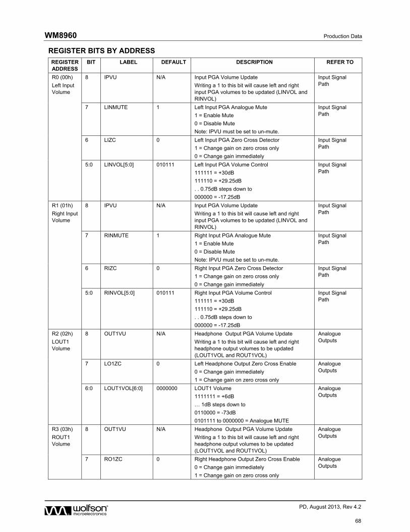
WM8960 Production Data
w PD, August 2013, Rev 4.2
68
REGISTER BITS BY ADDRESS
REGISTER ADDRESS
BIT LABEL DEFAULT DESCRIPTION REFER TO
R0 (00h)
Left Input Volume
8 IPVU N/A Input PGA Volume Update
Writing a 1 to this bit will cause left and right input PGA volumes to be updated (LINVOL and RINVOL)
Input Signal Path
7 LINMUTE 1 Left Input PGA Analogue Mute
1 = Enable Mute
0 = Disable Mute
Note: IPVU must be set to un-mute.
Input Signal Path
6 LIZC 0 Left Input PGA Zero Cross Detector
1 = Change gain on zero cross only
0 = Change gain immediately
Input Signal Path
5:0 LINVOL[5:0] 010111 Left Input PGA Volume Control
111111 = +30dB
111110 = +29.25dB
. . 0.75dB steps down to
000000 = -17.25dB
Input Signal Path
R1 (01h)
Right Input Volume
8 IPVU N/A Input PGA Volume Update
Writing a 1 to this bit will cause left and right input PGA volumes to be updated (LINVOL and RINVOL)
Input Signal Path
7 RINMUTE 1 Right Input PGA Analogue Mute
1 = Enable Mute
0 = Disable Mute
Note: IPVU must be set to un-mute.
Input Signal Path
6 RIZC 0 Right Input PGA Zero Cross Detector
1 = Change gain on zero cross only
0 = Change gain immediately
Input Signal Path
5:0 RINVOL[5:0] 010111 Right Input PGA Volume Control
111111 = +30dB
111110 = +29.25dB
. . 0.75dB steps down to
000000 = -17.25dB
Input Signal Path
R2 (02h)
LOUT1 Volume
8 OUT1VU N/A Headphone Output PGA Volume Update
Writing a 1 to this bit will cause left and right headphone output volumes to be updated (LOUT1VOL and ROUT1VOL)
Analogue Outputs
7 LO1ZC 0 Left Headphone Output Zero Cross Enable
0 = Change gain immediately
1 = Change gain on zero cross only
Analogue Outputs
6:0 LOUT1VOL[6:0] 0000000 LOUT1 Volume
1111111 = +6dB
… 1dB steps down to
0110000 = -73dB
0101111 to 0000000 = Analogue MUTE
Analogue Outputs
R3 (03h)
ROUT1 Volume
8 OUT1VU N/A Headphone Output PGA Volume Update
Writing a 1 to this bit will cause left and right headphone output volumes to be updated (LOUT1VOL and ROUT1VOL)
Analogue Outputs
7 RO1ZC 0 Right Headphone Output Zero Cross Enable
0 = Change gain immediately
1 = Change gain on zero cross only
Analogue Outputs

Production Data WM8960
w PD, August 2013, Rev 4.2
69
REGISTER ADDRESS
BIT LABEL DEFAULT DESCRIPTION REFER TO
6:0 ROUT1VOL[6:0] 0000000 ROUT1 Volume
1111111 = +6dB
… 1dB steps down to
0110000 = -73dB
0101111 to 0000000 = Analogue MUTE
Analogue Outputs
R4 (04h)
Clocking (1)
8:6 ADCDIV[2:0] 000 ADC Sample rate divider (Also determines ADCLRC in master mode)
000 = SYSCLK / (1.0 * 256)
001 = SYSCLK / (1.5 * 256)
010 = SYSCLK / (2 * 256)
011 = SYSCLK / (3 * 256)
100 = SYSCLK / (4 * 256)
101 = SYSCLK / (5.5 * 256)
110 = SYSCLK / (6 * 256)
111 = Reserved
Clocking and Sample Rates
5:3 DACDIV[2:0] 000 DAC Sample rate divider (Also determines DACLRC in master mode)
000 = SYSCLK / (1.0 * 256)
001 = SYSCLK / (1.5 * 256)
010 = SYSCLK / (2 * 256)
011 = SYSCLK / (3 * 256)
100 = SYSCLK / (4 * 256)
101 = SYSCLK / (5.5 * 256)
110 = SYSCLK / (6 * 256)
111 = Reserved
Clocking and Sample Rates
2:1 SYSCLKDIV[1:0] 00 SYSCLK Pre-divider. Clock source (MCLK or PLL output) will be divided by this value to generate SYSCLK.
00 = Divide SYSCLK by 1
01 = Reserved
10 = Divide SYSCLK by 2
11 = Reserved
Clocking and Sample Rates
0 CLKSEL 0 SYSCLK Selection
0 = SYSCLK derived from MCLK
1 = SYSCLK derived from PLL output
Clocking and Sample Rates
R5 (05h)
ADC and DAC Control (1)
8 0 Reserved
7 DACDIV2 0 DAC 6dB Attenuate Enable
0 = Disabled (0dB)
1 = -6dB Enabled
Output Signal Path
6:5 ADCPOL[1:0] 00 ADC polarity control:
00 = Polarity not inverted
01 = ADC L inverted
10 = ADC R inverted
11 = ADC L and R inverted
Analogue to Digital Converter
4 0 Reserved
3 DACMU 1 DAC Digital Soft Mute
1 = Mute
0 = No mute (signal active)
Output Signal Path
2:1 DEEMPH[1:0] 00 De-emphasis Control
11 = 48kHz sample rate
10 = 44.1kHz sample rate
01 = 32kHz sample rate
00 = No de-emphasis
Output Signal Path

WM8960 Production Data
w PD, August 2013, Rev 4.2
70
REGISTER ADDRESS
BIT LABEL DEFAULT DESCRIPTION REFER TO
0 ADCHPD 0 ADC High Pass Filter Disable
0 = Enable high pass filter on left and right channels
1 = Disable high pass filter on left and right channels
Analogue to Digital Converter
R6 (06h)
ADC and DAC Control (2)
8:7 00 Reserved
6:5 DACPOL[1:0] 00 DAC polarity control:
00 = Polarity not inverted
01 = DAC L inverted
10 = DAC R inverted
11 = DAC L and R inverted
Output Signal Path
4 0 Reserved
3 DACSMM 0 DAC Soft Mute Mode
0 = Disabling soft-mute (DACMU=0) will cause the volume to change immediately to the LDACVOL / RDACVOL settings
1 = Disabling soft-mute (DACMU=0) will cause the volume to ramp up gradually to the LDACVOL / RDACVOL settings
Output Signal Path
2 DACMR 0 DAC Soft Mute Ramp Rate
0 = Fast ramp (24kHz at fs=48k, providing maximum delay of 10.7ms)
1 = Slow ramp (1.5kHz at fs=48k, providing maximum delay of 171ms)
Output Signal Path
1 DACSLOPE 0 Selects DAC filter characteristics
0 = Normal mode
1 = Sloping stopband
Output Signal Path
0 0 Reserved
R7 (07h)
Audio Interface
8 ALRSWAP 0 Left/Right ADC Channel Swap
1 = Swap left and right ADC data in audio interface
0 = Output left and right data as normal
Audio Interface Control
7 BCLKINV 0 BCLK invert bit (for master and slave modes)
0 = BCLK not inverted
1 = BCLK inverted
Audio Interface Control
6 MS 0 Master / Slave Mode Control
0 = Enable slave mode
1 = Enable master mode
Audio Interface Control
5 DLRSWAP 0 Left/Right DAC Channel Swap
0 = Output left and right data as normal
1 = Swap left and right DAC data in audio interface
Audio Interface Control
4 LRP 0 Right, left and I2S modes – LRCLK polarity
0 = normal LRCLK polarity
1 = invert LRCLK polarity
Audio Interface Control
DSP Mode – mode A/B select
0 = MSB is available on 2nd BCLK rising edge after LRC rising edge (mode A)
1 = MSB is available on 1st BCLK rising edge after LRC rising edge (mode B)
3:2 WL[1:0] 10 Audio Data Word Length
00 = 16 bits
01 = 20 bits
10 = 24 bits
11 = 32 bits (see Note)
Audio Interface Control
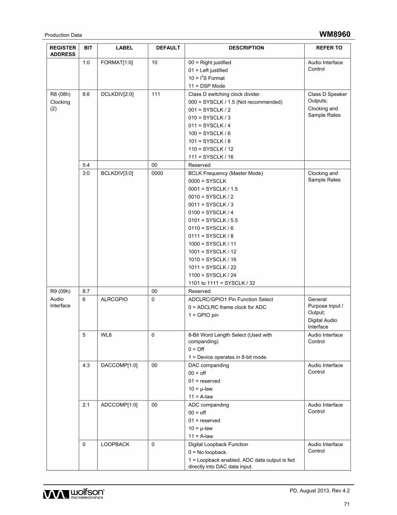
Production Data WM8960
w PD, August 2013, Rev 4.2
71
REGISTER ADDRESS
BIT LABEL DEFAULT DESCRIPTION REFER TO
1:0 FORMAT[1:0] 10 00 = Right justified
01 = Left justified
10 = I2S Format
11 = DSP Mode
Audio Interface Control
R8 (08h)
Clocking (2)
8:6 DCLKDIV[2:0] 111 Class D switching clock divider.
000 = SYSCLK / 1.5 (Not recommended)
001 = SYSCLK / 2
010 = SYSCLK / 3
011 = SYSCLK / 4
100 = SYSCLK / 6
101 = SYSCLK / 8
110 = SYSCLK / 12
111 = SYSCLK / 16
Class D Speaker Outputs;
Clocking and Sample Rates
5:4 00 Reserved
3:0 BCLKDIV[3:0] 0000 BCLK Frequency (Master Mode)
0000 = SYSCLK
0001 = SYSCLK / 1.5
0010 = SYSCLK / 2
0011 = SYSCLK / 3
0100 = SYSCLK / 4
0101 = SYSCLK / 5.5
0110 = SYSCLK / 6
0111 = SYSCLK / 8
1000 = SYSCLK / 11
1001 = SYSCLK / 12
1010 = SYSCLK / 16
1011 = SYSCLK / 22
1100 = SYSCLK / 24
1101 to 1111 = SYSCLK / 32
Clocking and Sample Rates
R9 (09h)
Audio Interface
8:7 00 Reserved
6 ALRCGPIO 0 ADCLRC/GPIO1 Pin Function Select
0 = ADCLRC frame clock for ADC
1 = GPIO pin
General Purpose Input / Output;
Digital Audio Interface
5 WL8 0 8-Bit Word Length Select (Used with companding)
0 = Off
1 = Device operates in 8-bit mode.
Audio Interface Control
4:3 DACCOMP[1:0] 00 DAC companding
00 = off
01 = reserved
10 = µ-law
11 = A-law
Audio Interface Control
2:1 ADCCOMP[1:0] 00 ADC companding
00 = off
01 = reserved
10 = µ-law
11 = A-law
Audio Interface Control
0 LOOPBACK 0 Digital Loopback Function
0 = No loopback.
1 = Loopback enabled, ADC data output is fed directly into DAC data input.
Audio Interface Control

WM8960 Production Data
w PD, August 2013, Rev 4.2
72
REGISTER ADDRESS
BIT LABEL DEFAULT DESCRIPTION REFER TO
R10 (0Ah)
Left DAC Volume
8 DACVU N/A DAC Volume Update
Writing a 1 to this bit will cause left and right DAC volumes to be updated (LDACVOL and RDACVOL)
Output Signal Path
7:0 LDACVOL[7:0] 11111111 Left DAC Digital Volume Control
0000 0000 = Digital Mute
0000 0001 = -127dB
0000 0010 = -126.5dB
... 0.5dB steps up to
1111 1111 = 0dB
Output Signal Path
R11 (0Bh)
Right DAC Volume
8 DACVU N/A DAC Volume Update
Writing a 1 to this bit will cause left and right DAC volumes to be updated (LDACVOL and RDACVOL)
Output Signal Path
7:0 RDACVOL[7:0] 11111111 Right DAC Digital Volume Control
0000 0000 = Digital Mute
0000 0001 = -127dB
0000 0010 = -126.5dB
... 0.5dB steps up to
1111 1111 = 0dB
Output Signal Path
R12 (0Ch) 8:0 000000000 Reserved
R13 (0Dh) 8:0 000000000 Reserved
R14 (0Eh) 8:0 000000000 Reserved
R15 (0Fh)
Reset
8:0 Reset N/A Writing to this register resets all registers to their default state.
R16 {10h)
3D Control
8 0 Reserved
7 0 Reserved
6 3DUC 0 3D Enhance Filter Upper Cut-Off Frequency
0 = High (Recommended for fs>=32kHz)
1 = Low (Recommended for fs<32kHz)
Output Signal Path
5 3DLC 0 3D Enhance Filter Lower Cut-Off Frequency
0 = Low (Recommended for fs>=32kHz)
1 = High (Recommended for fs<32kHz)
Output Signal Path
4:1 3DDEPTH[3:0] 0000 3D Stereo Depth
0000 = 0% (minimum 3D effect)
0001 = 6.67%
....
1110 = 93.3%
1111 = 100% (maximum 3D effect)
Output Signal Path
0 3DEN 0 3D Stereo Enhancement Enable
0 = Disabled
1 = Enabled
Output Signal Path
R17 (11h)
ALC (1)
8:7 ALCSEL[1:0] 00 ALC Function Select
00 = ALC off (PGA gain set by register)
01 = Right channel only
10 = Left channel only
11 = Stereo (PGA registers unused) Note: ensure that LINVOL and RINVOL settings (reg. 0 and 1) are the same before entering this mode.
Automatic Level Control

Production Data WM8960
w PD, August 2013, Rev 4.2
73
REGISTER ADDRESS
BIT LABEL DEFAULT DESCRIPTION REFER TO
6:4 MAXGAIN[2:0] 0000 Set Maximum Gain of PGA (During ALC operation)
111 : +30dB
110 : +24dB
….(-6dB steps)
001 : -6dB
000 : -12dB
Automatic Level Control
3:0 ALCL[3:0] 1011 ALC Target (Sets signal level at ADC input)
0000 = -22.5dB FS
0001 = -21.0dB FS
… (1.5dB steps)
1101 = -3.0dB FS
1110 = -1.5dB FS
1111 = -1.5dB FS
Automatic Level Control
R18 (12h)
ALC (2)
8 1 Reserved
7 0 Reserved
6:4 MINGAIN[2:0] 000 Set Minimum Gain of PGA (During ALC operation)
000 = -17.25dB
001 = -11.25dB
010 = -5.25dB
011 = +0.75dB
100 = +6.75dB
101 = +12.75dB
110 = +18.75dB
111 = +24.75dB
Automatic Level Control
3:0 HLD[3:0] 0000 ALC hold time before gain is increased.
0000 = 0ms
0001 = 2.67ms
0010 = 5.33ms
… (time doubles with every step)
1111 = 43.691s
Automatic Level Control
R19 (13h)
ALC (3)
8 ALCMODE 0 Determines the ALC mode of operation:
0 = ALC mode
1 = Limiter mode
Automatic Level Control
7:4 DCY[3:0] 0011 ALC decay (gain ramp-up) time
0000 = 24ms
0001 = 48ms
0010 = 96ms
… (time doubles with every step)
1010 or higher = 24.58s
Automatic Level Control
3:0 ATK[3:0] 0010 ALC attack (gain ramp-down) time
0000 = 6ms
0001 = 12ms
0010 = 24ms
… (time doubles with every step)
1010 or higher = 6.14s
Automatic Level Control
R20 (14h)
Noise Gate
8 0 Reserved
7:3 NGTH[4:0] 00000 Noise gate threshold
00000 -76.5dBfs
00001 -75dBfs
… 1.5 dB steps
11110 -31.5dBfs
11111 -30dBfs
Automatic Level Control
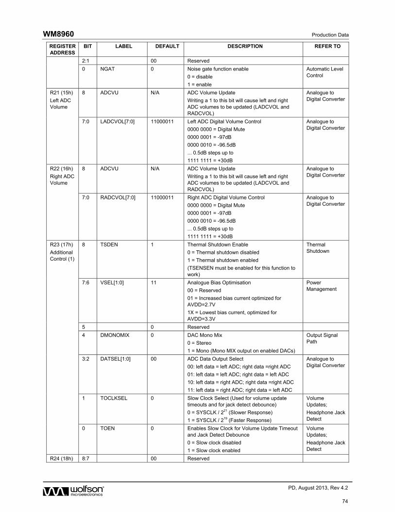
WM8960 Production Data
w PD, August 2013, Rev 4.2
74
REGISTER ADDRESS
BIT LABEL DEFAULT DESCRIPTION REFER TO
2:1 00 Reserved
0 NGAT 0 Noise gate function enable
0 = disable
1 = enable
Automatic Level Control
R21 (15h)
Left ADC Volume
8 ADCVU N/A ADC Volume Update
Writing a 1 to this bit will cause left and right ADC volumes to be updated (LADCVOL and RADCVOL)
Analogue to Digital Converter
7:0 LADCVOL[7:0] 11000011 Left ADC Digital Volume Control
0000 0000 = Digital Mute
0000 0001 = -97dB
0000 0010 = -96.5dB
... 0.5dB steps up to
1111 1111 = +30dB
Analogue to Digital Converter
R22 (16h)
Right ADC Volume
8 ADCVU N/A ADC Volume Update
Writing a 1 to this bit will cause left and right ADC volumes to be updated (LADCVOL and RADCVOL)
Analogue to Digital Converter
7:0 RADCVOL[7:0] 11000011 Right ADC Digital Volume Control
0000 0000 = Digital Mute
0000 0001 = -97dB
0000 0010 = -96.5dB
... 0.5dB steps up to
1111 1111 = +30dB
Analogue to Digital Converter
R23 (17h)
Additional Control (1)
8 TSDEN 1 Thermal Shutdown Enable
0 = Thermal shutdown disabled
1 = Thermal shutdown enabled
(TSENSEN must be enabled for this function to work)
Thermal Shutdown
7:6 VSEL[1:0] 11 Analogue Bias Optimisation
00 = Reserved
01 = Increased bias current optimized for AVDD=2.7V
1X = Lowest bias current, optimized for AVDD=3.3V
Power Management
5 0 Reserved
4 DMONOMIX 0 DAC Mono Mix
0 = Stereo
1 = Mono (Mono MIX output on enabled DACs)
Output Signal Path
3:2 DATSEL[1:0] 00 ADC Data Output Select
00: left data = left ADC; right data =right ADC
01: left data = left ADC; right data = left ADC
10: left data = right ADC; right data =right ADC
11: left data = right ADC; right data = left ADC
Analogue to Digital Converter
1 TOCLKSEL 0 Slow Clock Select (Used for volume update timeouts and for jack detect debounce)
0 = SYSCLK / 221 (Slower Response)
1 = SYSCLK / 219 (Faster Response)
Volume Updates;
Headphone Jack Detect
0 TOEN 0 Enables Slow Clock for Volume Update Timeout and Jack Detect Debounce
0 = Slow clock disabled
1 = Slow clock enabled
Volume Updates;
Headphone Jack Detect
R24 (18h) 8:7 00 Reserved

Production Data WM8960
w PD, August 2013, Rev 4.2
75
REGISTER ADDRESS
BIT LABEL DEFAULT DESCRIPTION REFER TO
Additional Control (2)
6 HPSWEN 0 Headphone Switch Enable
0 = Headphone switch disabled
1 = Headphone switch enabled
Headphone Jack Detect
5 HPSWPOL 0 Headphone Switch Polarity
0 = HPDETECT high = headphone
1 = HPDETECT high = speaker
Headphone Jack Detect
4 Reserved
3 TRIS 0 Tristates ADCDAT and switches ADCLRC, DACLRC and BCLK to inputs.
0 = ADCDAT is an output; ADCLRC, DACLRC and BCLK are inputs (slave mode) or outputs (master mode)
1 = ADCDAT is tristated; DACLRC and BCLK are inputs; ADCLRC is an input (when not configured as a GPIO)
Audio Interface Control
2 LRCM 0 Selects disable mode for ADCLRC and DACLRC (Master mode)
0 = ADCLRC disabled when ADC (Left and Right) disabled; DACLRC disabled when DAC (Left and Right) disabled.
1 = ADCLRC and DACLRC disabled only when ADC (Left and Right) and DAC (Left and Right) are disabled.
Audio Interface Control
1:0 0 Reserved
R25 (19h)
Power Mgmt (1)
8:7 VMIDSEL[1:0] 00 Vmid Divider Enable and Select
00 = Vmid disabled (for OFF mode)
01 = 2 x 50k divider enabled (for playback / record)
10 = 2 x 250k divider enabled (for low-power standby)
11 = 2 x 5k divider enabled (for fast start-up)
Power Management
6 VREF 0 VREF (necessary for all other functions)
0 = Power down
1 = Power up
Power Management
5 AINL 0 Analogue in PGA Left
0 = Power down
1 = Power up
Power Management
4 AINR 0 Analogue in PGA Right
0 = Power down
1 = Power up
Power Management
3 ADCL 0 ADC Left
0 = Power down
1 = Power up
Power Management
2 ADCR 0 ADC Right
0 = Power down
1 = Power up
Power Management
1 MICB 0 MICBIAS
0 = Power down
1 = Power up
Power Management
0 DIGENB 0 Master Clock Disable
0 = Master clock enabled
1 = Master clock disabled
Power Management
R26 (1Ah)
Power Mgmt (2)
8 DACL 0 DAC Left
0 = Power down
1 = Power up
Power Management
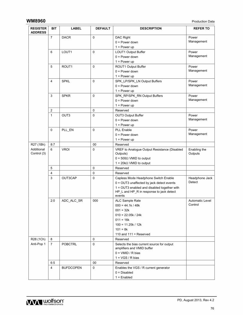
WM8960 Production Data
w PD, August 2013, Rev 4.2
76
REGISTER ADDRESS
BIT LABEL DEFAULT DESCRIPTION REFER TO
7 DACR 0 DAC Right
0 = Power down
1 = Power up
Power Management
6 LOUT1 0 LOUT1 Output Buffer
0 = Power down
1 = Power up
Power Management
5 ROUT1 0 ROUT1 Output Buffer
0 = Power down
1 = Power up
Power Management
4 SPKL 0 SPK_LP/SPK_LN Output Buffers
0 = Power down
1 = Power up
Power Management
3 SPKR 0 SPK_RP/SPK_RN Output Buffers
0 = Power down
1 = Power up
Power Management
2 0 Reserved
1 OUT3 0 OUT3 Output Buffer
0 = Power down
1 = Power up
Power Management
0 PLL_EN 0 PLL Enable
0 = Power down
1 = Power up
Power Management
R27 (1Bh)
Additional Control (3)
8:7 00 Reserved
6 VROI 0 VREF to Analogue Output Resistance (Disabled Outputs)
0 = 500 VMID to output
1 = 20k VMID to output
Enabling the Outputs
5 0 Reserved
4 0 Reserved
3 OUT3CAP 0 Capless Mode Headphone Switch Enable
0 = OUT3 unaffected by jack detect events
1 = OUT3 enabled and disabled together with HP_L and HP_R in response to jack detect events
Headphone Jack Detect
2:0 ADC_ALC_SR 000 ALC Sample Rate
000 = 44.1k / 48k
001 = 32k
010 = 22.05k / 24k
011 = 16k
100 = 11.25k / 12k
101 = 8k
110 and 111 = Reserved
Automatic Level Control
R28 (1Ch)
Anti-Pop 1
8 0 Reserved
7 POBCTRL 0 Selects the bias current source for output amplifiers and VMID buffer
0 = VMID / R bias
1 = VGS / R bias
6:5 00 Reserved
4 BUFDCOPEN 0 Enables the VGS / R current generator
0 = Disabled
1 = Enabled

Production Data WM8960
w PD, August 2013, Rev 4.2
77
REGISTER ADDRESS
BIT LABEL DEFAULT DESCRIPTION REFER TO
3 BUFIOEN 0 Enables the VGS / R current generator and the analogue input and output bias
0 = Disabled
1 = Enabled
2 SOFT_ST 0 Enables VMID soft start
0 = Disabled
1 = Enabled
1 0 Reserved
0 HPSTBY 0 Headphone Amplifier Standby
0 = Standby mode disabled (Normal operation)
1 = Standby mode enabled
R29 (1Dh)
Anti-pop 2
8:7 00 Reserved
6 DISOP 0 Discharges the DC-blocking headphone capacitors on HP_L and HP_R
0 = Disabled
1 = Enabled
5:4 DRES[1:0] 00 DRES determines the value of the resistors used to discharge the DC-blocking headphone capacitors when DISOP=1
DRES[1:0] Resistance (Ohms)
0 0 400
0 1 200
1 0 600
1 1 150
3:0 0000 Reserved
R30 (1Eh) 8:0 000000000 Reserved
R31 (1Fh) 8:0 000000000 Reserved
R32 (20h)
ADCL Signal Path
8 LMN1 1 Connect LINPUT1 to inverting input of Left Input PGA
0 = LINPUT1 not connected to PGA
1 = LINPUT1 connected to PGA
Input Signal Path
7 LMP3 0 Connect LINPUT3 to non-inverting input of Left Input PGA
0 = LINPUT3 not connected to PGA
1 = LINPUT3 connected to PGA (Constant input impedance)
Input Signal Path
6 LMP2 0 Connect LINPUT2 to non-inverting input of Left Input PGA
0 = LINPUT2 not connected to PGA
1 = LINPUT2 connected to PGA (Constant input impedance)
Input Signal Path
5:4 LMICBOOST[1:0] 00 Left Channel Input PGA Boost Gain
00 = +0dB
01 = +13dB
10 = +20dB
11 = +29dB
Input Signal Path
3 LMIC2B 0 Connect Left Input PGA to Left Input Boost Mixer
0 = Not connected
1 = Connected
Input Signal Path
2:0 000 Reserved
R33 (21h)
ADCR Signal Path
8 RMN1 1 Connect RINPUT1 to inverting input of Right Input PGA
0 = RINPUT1 not connected to PGA
1 = RINPUT1 connected to PGA
Input Signal Path
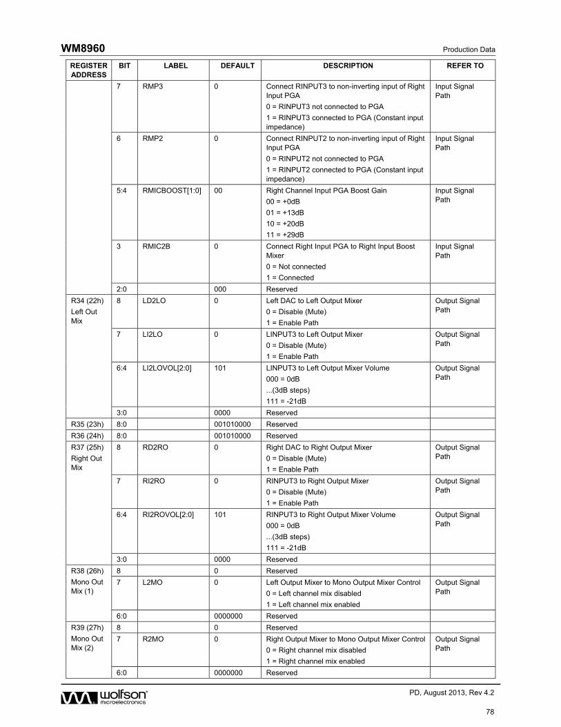
WM8960 Production Data
w PD, August 2013, Rev 4.2
78
REGISTER ADDRESS
BIT LABEL DEFAULT DESCRIPTION REFER TO
7 RMP3 0 Connect RINPUT3 to non-inverting input of Right Input PGA
0 = RINPUT3 not connected to PGA
1 = RINPUT3 connected to PGA (Constant input impedance)
Input Signal Path
6 RMP2 0 Connect RINPUT2 to non-inverting input of Right Input PGA
0 = RINPUT2 not connected to PGA
1 = RINPUT2 connected to PGA (Constant input impedance)
Input Signal Path
5:4 RMICBOOST[1:0] 00 Right Channel Input PGA Boost Gain
00 = +0dB
01 = +13dB
10 = +20dB
11 = +29dB
Input Signal Path
3 RMIC2B 0 Connect Right Input PGA to Right Input Boost Mixer
0 = Not connected
1 = Connected
Input Signal Path
2:0 000 Reserved
R34 (22h)
Left Out Mix
8 LD2LO 0 Left DAC to Left Output Mixer
0 = Disable (Mute)
1 = Enable Path
Output Signal Path
7 LI2LO 0 LINPUT3 to Left Output Mixer
0 = Disable (Mute)
1 = Enable Path
Output Signal Path
6:4 LI2LOVOL[2:0] 101 LINPUT3 to Left Output Mixer Volume
000 = 0dB
...(3dB steps)
111 = -21dB
Output Signal Path
3:0 0000 Reserved
R35 (23h) 8:0 001010000 Reserved
R36 (24h) 8:0 001010000 Reserved
R37 (25h)
Right Out Mix
8 RD2RO 0 Right DAC to Right Output Mixer
0 = Disable (Mute)
1 = Enable Path
Output Signal Path
7 RI2RO 0 RINPUT3 to Right Output Mixer
0 = Disable (Mute)
1 = Enable Path
Output Signal Path
6:4 RI2ROVOL[2:0] 101 RINPUT3 to Right Output Mixer Volume
000 = 0dB
...(3dB steps)
111 = -21dB
Output Signal Path
3:0 0000 Reserved
R38 (26h)
Mono Out Mix (1)
8 0 Reserved
7 L2MO 0 Left Output Mixer to Mono Output Mixer Control
0 = Left channel mix disabled
1 = Left channel mix enabled
Output Signal Path
6:0 0000000 Reserved
R39 (27h)
Mono Out Mix (2)
8 0 Reserved
7 R2MO 0 Right Output Mixer to Mono Output Mixer Control
0 = Right channel mix disabled
1 = Right channel mix enabled
Output Signal Path
6:0 0000000 Reserved

Production Data WM8960
w PD, August 2013, Rev 4.2
79
REGISTER ADDRESS
BIT LABEL DEFAULT DESCRIPTION REFER TO
R40 (28h)
Left Speaker Volume
8 SPKVU N/A Speaker Volume Update
Writing a 1 to this bit will cause left and right speaker volumes to be updated (SPKLVOL and SPKRVOL)
Analogue Outputs
7 SPKLZC 0 Left Speaker Zero Cross Enable
1 = Change gain on zero cross only
0 = Change gain immediately
Analogue Outputs
6:0 SPKLVOL[6:0] 0000000 SPK_LP/SPK_LN Volume
1111111 = +6dB
… 1dB steps down to
0110000 = -73dB
0101111 to 0000000 = Analogue MUTE
Analogue Outputs
R41 (29h)
Right Speaker Volume
8 SPKVU N/A Speaker Volume Update
Writing a 1 to this bit will cause left and right speaker volumes to be updated (SPKLVOL and SPKRVOL)
Analogue Outputs
7 SPKRZC 0 Right Speaker Zero Cross Enable
1 = Change gain on zero cross only
0 = Change gain immediately
Analogue Outputs
6:0 SPKRVOL[6:0] 0000000 SPK_RP/SPK_RN Volume
1111111 = +6dB
… 1dB steps down to
0110000 = -73dB
0101111 to 0000000 = Analogue MUTE
Analogue Outputs
R42 (2Ah)
OUT3 Volume
8:7 00 Reserved
6 MOUTVOL 1 Mono Output Mixer Volume Control
0 = 0dB
1 = -6dB
Output Signal Path
5:0 000000 Reserved
R43 (2Bh)
Left Input Boost Mixer
8:7 00 Reserved
6:4 LIN3BOOST[2:0] 000 LINPUT3 to Boost Mixer Gain
000 = Mute
001 = -12dB
...3dB steps up to
111 = +6dB
Input Signal Path
3:1 LIN2BOOST[2:0] 000 LINPUT2 to Boost Mixer Gain
000 = Mute
001 = -12dB
...3dB steps up to
111 = +6dB
Input Signal Path
0 0 Reserved
R44 (2Ch)
Right Input Boost Mixer
8:7 00 Reserved
6:4 RIN3BOOST[2:0] 000 RINPUT3 to Boost Mixer Gain
000 = Mute
001 = -12dB
...3dB steps up to
111 = +6dB
Input Signal Path
3:1 RIN2BOOST[2:0] 000 RINPUT2 to Boost Mixer Gain
000 = Mute
001 = -12dB
...3dB steps up to
111 = +6dB
Input Signal Path
0 0 Reserved
R45 (2Dh) 8 0 Reserved

WM8960 Production Data
w PD, August 2013, Rev 4.2
80
REGISTER ADDRESS
BIT LABEL DEFAULT DESCRIPTION REFER TO
Left Bypass
7 LB2LO 0 Left Input Boost Mixer to Left Output Mixer
0 = Disable (Mute)
1 = Enable Path
Output Signal Path
6:4 LB2LOVOL[2:0] 101 Left Input Boost Mixer to Left Output Mixer Volume
000 = 0dB
...(3dB steps)
111 = -21dB
Output Signal Path
3:0 0000 Reserved
R46 (2Eh)
Right Bypass
8 0 Reserved
7 RB2RO 0 Right Input Boost Mixer to Right Output Mixer
0 = Disable (Mute)
1 = Enable Path
Output Signal Path
6:4 RB2ROVOL[2:0] 101 Right Input Boost Mixer to Right Output Mixer Volume
000 = 0dB
...(3dB steps)
111 = -21dB
Output Signal Path
3:0 0000 Reserved
R47 (2Fh)
Power Mgmt (3)
8:6 000 Reserved
5 LMIC 0 Left Channel Input PGA Enable
0 = PGA disabled
1 = PGA enabled (if AINL = 1)
Input Signal Path
4 RMIC 0 Right Channel Input PGA Enable
0 = PGA disabled
1 = PGA enabled (if AINR = 1)
Input Signal Path
3 LOMIX 0 Left Output Mixer Enable Control
0 = Disabled
1 = Enabled
Output Signal Path
2 ROMIX 0 Right Output Mixer Enable Control
0 = Disabled
1 = Enabled
Output Signal Path
1:0 00 Reserved
R48 (30h)
Additional Control (4)
8 0 Reserved
7 GPIOPOL 0 GPIO Polarity Invert
0 = Non inverted
1 = Inverted
General Purpose Input / Output
6:4 GPIOSEL[2:0] 000 ADCLRC/GPIO1 GPIO Function Select:
000 = Jack detect input
001 = Reserved
010 = Temperature ok
011 = Debounced jack detect output
100 = SYSCLK output
101 = PLL lock
110 = Logic 0
111 = Logic 1
General Purpose Input / Output
3:2 HPSEL[1:0] 00 Headphone Switch Input Select
0X = GPIO1 used for jack detect input (Requires ADCLRC pin to be configured as a GPIO)
10 = JD2 used for jack detect input
11 = JD3 used for jack detect input
Headphone Jack Detect
1 TSENSEN 1 Temperature Sensor Enable
0 = Temperature sensor disabled
1 = Temperature sensor enabled
Thermal Shutdown

Production Data WM8960
w PD, August 2013, Rev 4.2
81
REGISTER ADDRESS
BIT LABEL DEFAULT DESCRIPTION REFER TO
0 MBSEL 0 Microphone Bias Voltage Control
0 = 0.9 * AVDD
1 = 0.65 * AVDD
Input Signal Path
R49 (31h)
Class D Control (1)
8 0 Reserved
7:6 SPK_OP_EN[1:0] 00 Enable Class D Speaker Outputs
00 = Off
01 = Left speaker only
10 = Right speaker only
11 = Left and right speakers enabled
Enabling the Outputs
5:0 110111 Reserved
R50 (32h) 8:0 001001101 Reserved
R51 (33h)
Class D Control (2)
8:6 010 Reserved
5:3 DCGAIN[2:0] 000 DC Speaker Boost (Boosts speaker DC output level by up to 1.8 x on left and right channels)
000 = 1.00x boost (+0dB)
001 = 1.27x boost (+2.1dB)
010 = 1.40x boost (+2.9dB)
011 = 1.52x boost (+3.6dB)
100 = 1.67x boost (+4.5dB)
101 = 1.8x boost (+5.1dB)
110 to 111 = Reserved
Analogue Outputs
2:0 ACGAIN[2:0] 000 AC Speaker Boost (Boosts speaker AC output signal by up to 1.8 x on left and right channels)
000 = 1.00x boost (+0dB)
001 = 1.27x boost (+2.1dB)
010 = 1.40x boost (+2.9dB)
011 = 1.52x boost (+3.6dB)
100 = 1.67x boost (+4.5dB)
101 = 1.8x boost (+5.1dB)
110 to 111 = Reserved
Analogue Outputs
R52 (34h)
PLL (1)
8:6 OPCLKDIV[2:0] 000 SYSCLK Output to GPIO Clock Division ratio
000 = SYSCLK
001 = SYSCLK / 2
010 = SYSCLK / 3
011 = SYSCLK / 4
100 = SYSCLK / 5.5
101 = SYSCLK / 6
General Purpose Input / Output
5 SDM 0 Enable Integer Mode
0 = Integer mode
1 = Fractional mode
Clocking and Sample Rates
4 PLLPRESCALE 0 Divide MCLK by 2 before input to PLL
0 = Divide by 1
1 = Divide by 2
Clocking and Sample Rates
3:0 PLLN[3:0] 1000 Integer (N) part of PLL input/output frequency ratio. Use values greater than 5 and less than 13.
Clocking and Sample Rates
R53 (35h)
PLL (2)
8 0 Reserved
7:0 PLLK[23:16] 00110001 Fractional (K) part of PLL1 input/output frequency ratio (treat as one 24-digit binary number).
Clocking and Sample Rates
R54 (36h)
PLL (3)
8 0 Reserved
7:0 PLLK[15:8] 00100110 Fractional (K) part of PLL1 input/output frequency ratio (treat as one 24-digit binary number).
Clocking and Sample Rates
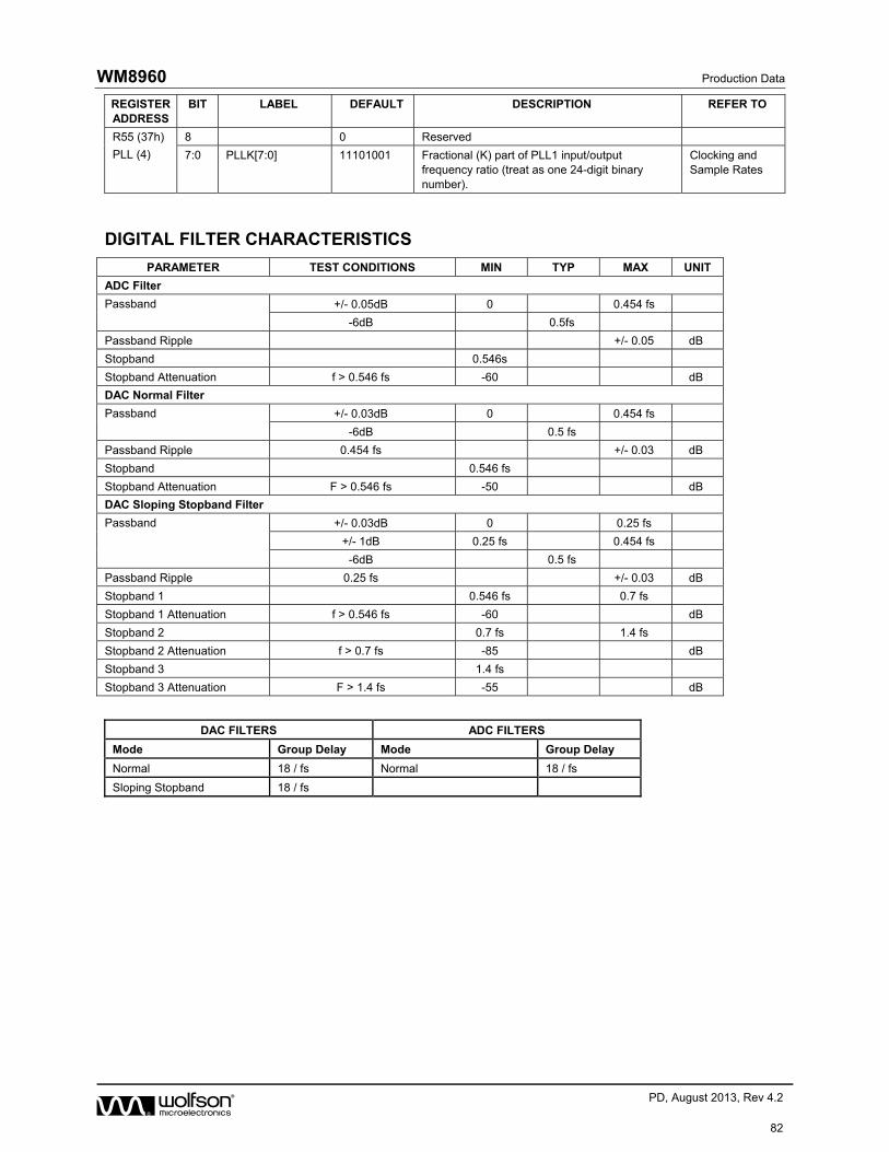
WM8960 Production Data
w PD, August 2013, Rev 4.2
82
REGISTER ADDRESS
BIT LABEL DEFAULT DESCRIPTION REFER TO
R55 (37h)
PLL (4)
8 0 Reserved
7:0 PLLK[7:0] 11101001 Fractional (K) part of PLL1 input/output frequency ratio (treat as one 24-digit binary number).
Clocking and Sample Rates
DIGITAL FILTER CHARACTERISTICS
PARAMETER TEST CONDITIONS MIN TYP MAX UNIT
ADC Filter
Passband +/- 0.05dB 0 0.454 fs
-6dB 0.5fs
Passband Ripple +/- 0.05 dB
Stopband 0.546s
Stopband Attenuation f > 0.546 fs -60 dB
DAC Normal Filter
Passband +/- 0.03dB 0 0.454 fs
-6dB 0.5 fs
Passband Ripple 0.454 fs +/- 0.03 dB
Stopband 0.546 fs
Stopband Attenuation F > 0.546 fs -50 dB
DAC Sloping Stopband Filter
Passband +/- 0.03dB 0 0.25 fs
+/- 1dB 0.25 fs 0.454 fs
-6dB 0.5 fs
Passband Ripple 0.25 fs +/- 0.03 dB
Stopband 1 0.546 fs 0.7 fs
Stopband 1 Attenuation f > 0.546 fs -60 dB
Stopband 2 0.7 fs 1.4 fs
Stopband 2 Attenuation f > 0.7 fs -85 dB
Stopband 3 1.4 fs
Stopband 3 Attenuation F > 1.4 fs -55 dB
DAC FILTERS ADC FILTERS
Mode Group Delay Mode Group Delay
Normal 18 / fs Normal 18 / fs
Sloping Stopband 18 / fs

Production Data WM8960
w PD, August 2013, Rev 4.2
83
ADC FILTER RESPONSES
-150
-130
-110
-90
-70
-50
-30
-10
10
0
0.1
0.2
0.3
0.4
0.5
1
0.6
1
0.7
1
0.8
1
0.9
1
1.0
1
1.1
1
1.2
1
1.3
1
1.4
2
1.5
2
1.6
2
1.7
2
1.8
2
1.9
2
2.0
2
2.1
2
2.2
2
2.3
3
2.4
3
2.5
3
2.6
3
2.7
3
2.8
3
2.9
3
3.0
3
3.1
3
3.2
4
3.3
4
3.4
4
3.5
4
3.6
4
3.7
4
3.8
4
3.9
4
Frequency (fs)
Ma
gn
itu
de
(d
B)
Magnitude (dB): Passband Ripple
-0.1
-0.08
-0.06
-0.04
-0.02
0
0.02
0.04
0.06
0.08
0.1
0.00 0.25
Frequency
Figure 38 ADC Digital Filter Frequency Response Figure 39 ADC Digital Filter Ripple
DAC FILTER RESPONSES
DAC STOPBAND ATTENUATION
The DAC digital filter type is selected by the DACSLOPE register bit as shown in Table 50.
REGISTER ADDRESS
BIT LABEL DEFAULT DESCRIPTION
R6 (06h)
ADC and DAC Control (2)
1 DACSLOPE 0 Selects DAC filter characteristics
0 = Normal mode
1 = Sloping stopband mode
Table 50 DAC Filter Selection
MAGNITUDE(dB)
-150
-130
-110
-90
-70
-50
-30
-10
10
0 0.5 1 1.5 2 2.5 3
Frequency (fs)
MAGNITUDE(dB)
-0.005
0
0.005
0.01
0.015
0.02
0.025
0.03
0.035
0.04
0 0.05 0.1 0.15 0.2 0.25 0.3 0.35 0.4 0.45 0.5
Frequency (fs)
Figure 40 DAC Digital Filter Frequency Response (Normal Mode)
Figure 41 DAC Digital Filter Ripple (Normal Mode)

WM8960 Production Data
w PD, August 2013, Rev 4.2
84
MAGNITUDE(dB)
-150
-130
-110
-90
-70
-50
-30
-10
10
0 0.5 1 1.5 2 2.5 3
Frequency (fs)
MAGNITUDE(dB)
-0.5
-0.45
-0.4
-0.35
-0.3
-0.25
-0.2
-0.15
-0.1
-0.05
0
0.05
0 0.05 0.1 0.15 0.2 0.25 0.3 0.35 0.4 0.45 0.5
Frequency (fs)
Figure 42 DAC Digital Filter Frequency Response (Sloping Stopband Mode)
Figure 43 DAC Digital Filter Ripple (Sloping Stopband Mode)
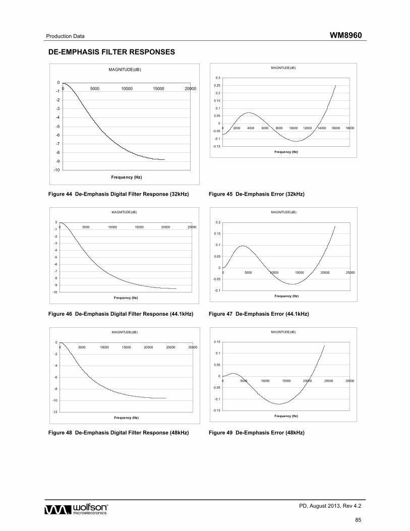
Production Data WM8960
w PD, August 2013, Rev 4.2
85
DE-EMPHASIS FILTER RESPONSES
MAGNITUDE(dB)
-10
-9
-8
-7
-6
-5
-4
-3
-2
-1
0
0 5000 10000 15000 20000
Frequency (Hz)
MAGNITUDE(dB)
-0.15
-0.1
-0.05
0
0.05
0.1
0.15
0.2
0.25
0.3
0 2000 4000 6000 8000 10000 12000 14000 16000 18000
Frequency (Hz)
Figure 44 De-Emphasis Digital Filter Response (32kHz) Figure 45 De-Emphasis Error (32kHz)
MAGNITUDE(dB)
-10
-9
-8
-7
-6
-5
-4
-3
-2
-1
0
0 5000 10000 15000 20000 25000
Frequency (Hz)
MAGNITUDE(dB)
-0.1
-0.05
0
0.05
0.1
0.15
0.2
0 5000 10000 15000 20000 25000
Frequency (Hz)
Figure 46 De-Emphasis Digital Filter Response (44.1kHz) Figure 47 De-Emphasis Error (44.1kHz)
MAGNITUDE(dB)
-12
-10
-8
-6
-4
-2
0
0 5000 10000 15000 20000 25000 30000
Frequency (Hz)
MAGNITUDE(dB)
-0.15
-0.1
-0.05
0
0.05
0.1
0.15
0 5000 10000 15000 20000 25000 30000
Frequency (Hz)
Figure 48 De-Emphasis Digital Filter Response (48kHz) Figure 49 De-Emphasis Error (48kHz)
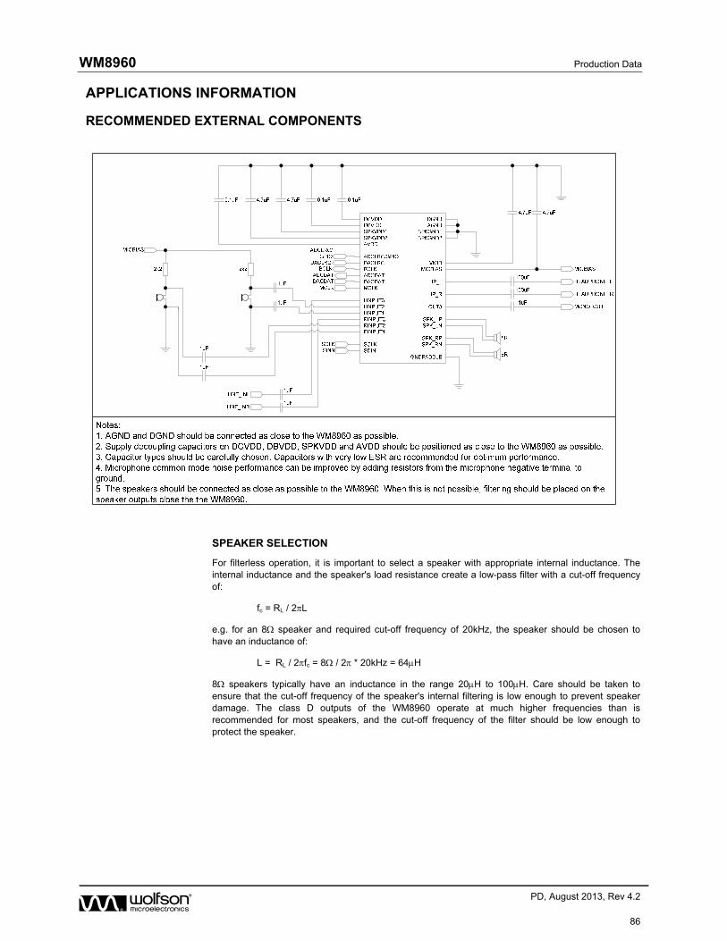
WM8960 Production Data
w PD, August 2013, Rev 4.2
86
APPLICATIONS INFORMATION
RECOMMENDED EXTERNAL COMPONENTS
SPEAKER SELECTION
For filterless operation, it is important to select a speaker with appropriate internal inductance. The internal inductance and the speaker's load resistance create a low-pass filter with a cut-off frequency of:
fc = RL / 2L
e.g. for an 8 speaker and required cut-off frequency of 20kHz, the speaker should be chosen to have an inductance of:
L = RL / 2fc = 8 / 2 * 20kHz = 64H
8 speakers typically have an inductance in the range 20H to 100H. Care should be taken to ensure that the cut-off frequency of the speaker's internal filtering is low enough to prevent speaker damage. The class D outputs of the WM8960 operate at much higher frequencies than is recommended for most speakers, and the cut-off frequency of the filter should be low enough to protect the speaker.

Production Data WM8960
w PD, August 2013, Rev 4.2
87
Figure 50 Speaker Equivalent Circuit
PCB LAYOUT CONSIDERATIONS
The efficiency of the speaker drivers is affected by the series resistance between the WM8960 and the speaker (e.g. inductor ESR) as shown in Figure 51. This resistance should be as low as possible to maximise efficiency.
Figure 51 Speaker Connection Losses
The distance between the WM8960 and the speakers should be kept to a minimum to reduce series resistance, and also to reduce EMI. Further reductions in EMI can be achieved by additional passive filtering and/or shielding as shown in Figure 52. When additional passive filtering is used, low ESR components should be chosen to minimise series resistance between the WM8960 and the speaker, maximising efficiency.
LC passive filtering will usually be effective at reducing EMI at frequencies up to around 30MHz. To reduce emissions at higher frequencies, ferrite beads placed as close to the device as possible will be more effective.
Note: Refer to the application note WAN_0118 on “Guidelines on How to Use QFN Packages and Create Associated PCB Footprints”

WM8960 Production Data
w PD, August 2013, Rev 4.2
88
Figure 52 EMI Reduction Techniques
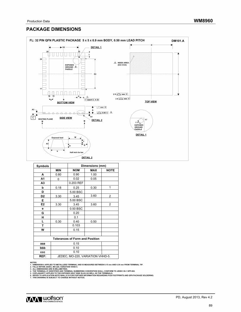
Production Data WM8960
w PD, August 2013, Rev 4.2
89
PACKAGE DIMENSIONS
DM101.AFL: 32 PIN QFN PLASTIC PACKAGE 5 X 5 X 0.9 mm BODY, 0.50 mm LEAD PITCH
E2
bB
16 15
8
9
e
C0.08
Cccc
A
A1C
A3
SEATING PLANE
1
L
INDEX AREA(D/2 X E/2)
TOP VIEW
D
Caaa2 X
Caaa2 X
E
1
17
24
25 32
D2
BCbbb M A
5
4
NOTES:1. DIMENSION b APPLIES TO METALLIZED TERMINAL AND IS MEASURED BETWEEN 0.15 mm AND 0.30 mm FROM TERMINAL TIP. 2. FALLS WITHIN JEDEC, MO-220, VARIATION VHHD-5. 3. ALL DIMENSIONS ARE IN MILLIMETRES.4. THE TERMINAL #1 IDENTIFIER AND TERMINAL NUMBERING CONVENTION SHALL CONFORM TO JEDEC 95-1 SPP-002.5. COPLANARITY APPLIES TO THE EXPOSED HEAT SINK SLUG AS WELL AS THE TERMINALS.6. REFER TO APPLICATION NOTE WAN_0118 FOR FURTHER INFORMATION REGARDING PCB FOOTPRINTS AND QFN PACKAGE SOLDERING.7. THIS DRAWING IS SUBJECT TO CHANGE WITHOUT NOTICE.
DETAIL 1
A3G
T
H
W
b
Exposed lead
Half etch tie bar
Dimensions (mm)Symbols
MIN NOM MAX NOTE
A
A1
A3
0.80 0.90 1.00
0.050.0200.203 REF
b
D
D2
EE2
e
L
0.300.18
5.00 BSC3.603.453.30
0.50 BSC
0.30 0.40 0.50
1
2
25.00 BSC
3.603.453.30
0.10
aaa
bbbccc
REF:
0.15
0.10
JEDEC, MO-220, VARIATION VHHD-5.
Tolerances of Form and Position
0.25
H 0.1
0.20G
T 0.103
W 0.15
DETAIL 1
DETAIL 2
DETAIL 2
EXPOSEDGROUND PADDLE
6
EXPOSED GROUNDPADDLE
BOTTOM VIEW
SIDE VIEW
0.30
45°M M
WM8960 Production Data
w PD, August 2013, Rev 4.2
90
IMPORTANT NOTICE
Wolfson Microelectronics plc (“Wolfson”) products and services are sold subject to Wolfson’s terms and conditions of sale, delivery and payment supplied at the time of order acknowledgement.
Wolfson warrants performance of its products to the specifications in effect at the date of shipment. Wolfson reserves the right to make changes to its products and specifications or to discontinue any product or service without notice. Customers should therefore obtain the latest version of relevant information from Wolfson to verify that the information is current.
Testing and other quality control techniques are utilised to the extent Wolfson deems necessary to support its warranty. Specific testing of all parameters of each device is not necessarily performed unless required by law or regulation.
In order to minimise risks associated with customer applications, the customer must use adequate design and operating safeguards to minimise inherent or procedural hazards. Wolfson is not liable for applications assistance or customer product design. The customer is solely responsible for its selection and use of Wolfson products. Wolfson is not liable for such selection or use nor for use of any circuitry other than circuitry entirely embodied in a Wolfson product.
Wolfson’s products are not intended for use in life support systems, appliances, nuclear systems or systems where malfunction can reasonably be expected to result in personal injury, death or severe property or environmental damage. Any use of products by the customer for such purposes is at the customer’s own risk.
Wolfson does not grant any licence (express or implied) under any patent right, copyright, mask work right or other intellectual property right of Wolfson covering or relating to any combination, machine, or process in which its products or services might be or are used. Any provision or publication of any third party’s products or services does not constitute Wolfson’s approval, licence, warranty or endorsement thereof. Any third party trade marks contained in this document belong to the respective third party owner.
Reproduction of information from Wolfson datasheets is permissible only if reproduction is without alteration and is accompanied by all associated copyright, proprietary and other notices (including this notice) and conditions. Wolfson is not liable for any unauthorised alteration of such information or for any reliance placed thereon.
Any representations made, warranties given, and/or liabilities accepted by any person which differ from those contained in this datasheet or in Wolfson’s standard terms and conditions of sale, delivery and payment are made, given and/or accepted at that person’s own risk. Wolfson is not liable for any such representations, warranties or liabilities or for any reliance placed thereon by any person.
ADDRESS:
Wolfson Microelectronics plc
26 Westfield Road
Edinburgh
EH11 2QB
United Kingdom
Tel :: +44 (0)131 272 7000
Fax :: +44 (0)131 272 7001
Email :: [email protected]

Production Data WM8960
w PD, August 2013, Rev 4.2
91
REVISION HISTORY
DATE REV ORIGINATOR CHANGES
23/09/11 4.1 JMacD Order codes changed from WM8960GEFL/V and WM8960GEFL/RV to WM8960CGEFL/V and WM8960CGEFL/RV to reflect change to copper wire bonding.
23/09/11 4.1 JMacD Package Diagram changed to DM101.A.
20/08/13 4.2 JMacD WM8960CGEFL/2RV added to Order Code information.