wmtech materials for micro- and nanotechnologies...
TRANSCRIPT
H.-J. Fecht, NST2B workshop, Warsaw Feb. 7.-9., 2007
WMtechMaterials for Micro- and NanotechnologiesExample of a public – private partnership
Hans FechtUlm University
Institute of Micro- and NanomaterialsAlbert-Einstein-Allee 47, 89081 Ulm, Germany
&Research Center Karlsruhe
Institute of Nanotechnology INT, Karlsruhe, Germany
H.-J. Fecht, NST2B workshop, Warsaw Feb. 7.-9., 2007
Overview
General Remarks
Example Science Park Ulm
WMtech – Materials center for micro & nanotechnology
Examples for Applications
Conclusions
H.-J. Fecht, NST2B workshop, Warsaw Feb. 7.-9., 2007
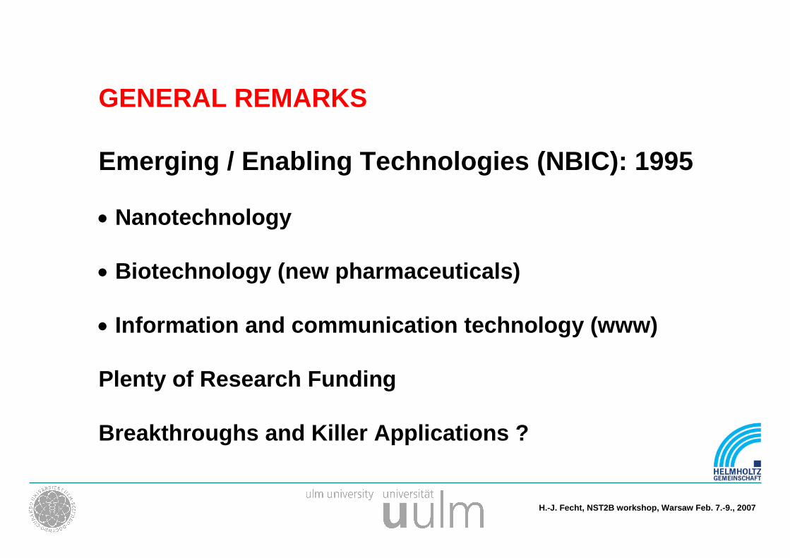
GENERAL REMARKS
Emerging / Enabling Technologies (NBIC): 1995
Nanotechnology
Biotechnology (new pharmaceuticals)
Information and communication technology (www)
Plenty of Research Funding
Breakthroughs and Killer Applications ?
H.-J. Fecht, NST2B workshop, Warsaw Feb. 7.-9., 2007
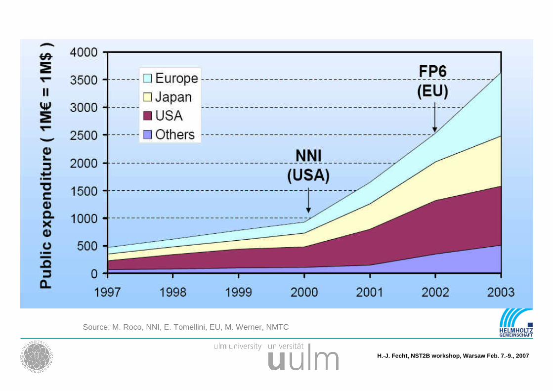
Source: M. Roco, NNI, E. Tomellini, EU, M. Werner, NMTC
H.-J. Fecht, NST2B workshop, Warsaw Feb. 7.-9., 2007
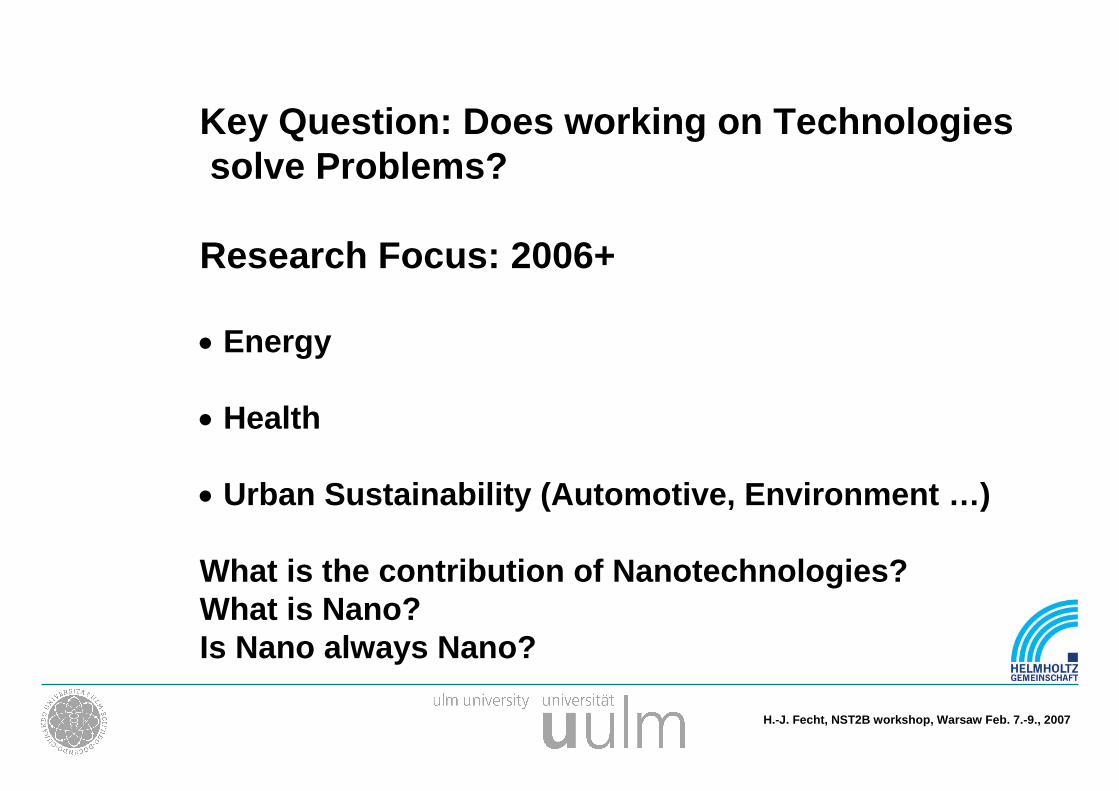
Key Question: Does working on Technologiessolve Problems?
Research Focus: 2006+
Energy
Health
Urban Sustainability (Automotive, Environment …)
What is the contribution of Nanotechnologies?What is Nano?Is Nano always Nano?
H.-J. Fecht, NST2B workshop, Warsaw Feb. 7.-9., 2007
Results / Success Stories ?
Biotech industries
Pharmaceuticals
Agricultural Chemistry
Very Focussed Applications, considered important
Same for ICT
H.-J. Fecht, NST2B workshop, Warsaw Feb. 7.-9., 2007
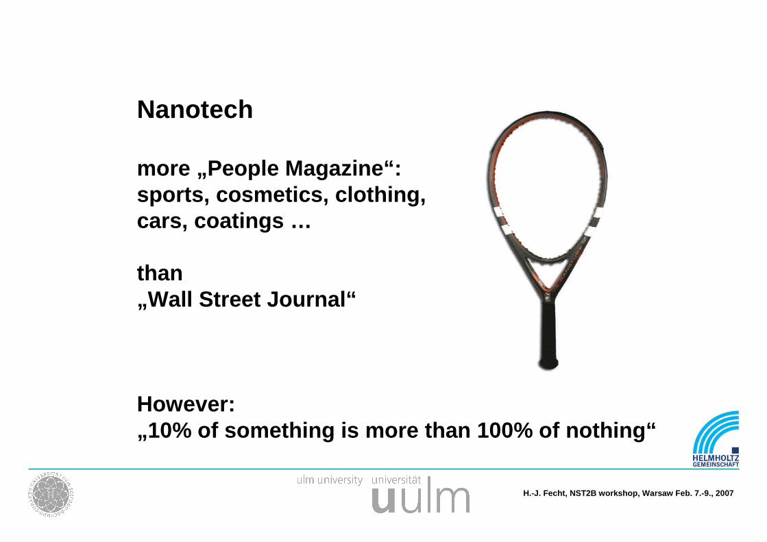
Nanotech
more „People Magazine“:sports, cosmetics, clothing,cars, coatings …
than„Wall Street Journal“
However:„10% of something is more than 100% of nothing“
H.-J. Fecht, NST2B workshop, Warsaw Feb. 7.-9., 2007
How about Nanotech industries
47% of Nanotech market are Nanomaterials
New trends, CNT, other nanotubes, nanocomposites...
Nanotools
Products based on nanotech
U.S. patent office: search nano- materials, chemicals- no electronics, no pharmaceutical

H.-J. Fecht, NST2B workshop, Warsaw Feb. 7.-9., 2007
NanoTech „glamorous“ applications ?
feeds traditional markets
long lead time (10-15 ys.)
no fundamentally new products
improved performance
improved lifetime
marginal improvement unlike biotech

H.-J. Fecht, NST2B workshop, Warsaw Feb. 7.-9., 2007
VC‘s generally do not understand markets
IT – health ok (telephone, cancer research)
Problems encountered:
No evaluation of nanotech was available at the startof the nano-hype
Patent situation confusing (interdisciplinary)
Segmented and often small markets
VC does not invest

H.-J. Fecht, NST2B workshop, Warsaw Feb. 7.-9., 2007
Conclusion / Solution
Financing by conventional means
Sales
Angels – Private Investors
Cooperation
Public Funding
H.-J. Fecht, NST2B workshop, Warsaw Feb. 7.-9., 2007
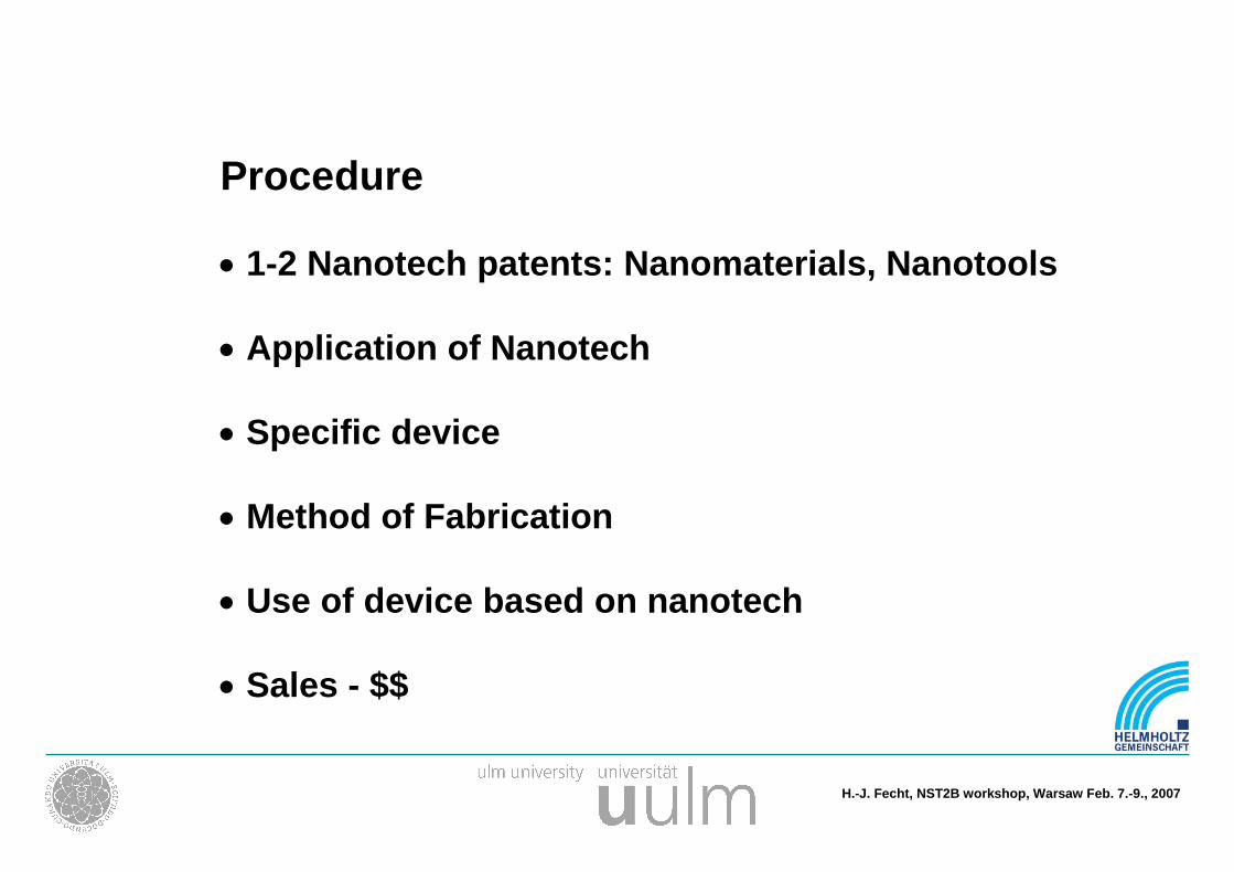
Procedure
1-2 Nanotech patents: Nanomaterials, Nanotools
Application of Nanotech
Specific device
Method of Fabrication
Use of device based on nanotech
Sales - $$

H.-J. Fecht, NST2B workshop, Warsaw Feb. 7.-9., 2007
AdvancedMaterialsSystems
InformationTechnology withNanoelectronic
Systems
Nanotechnology
Microoptics
„NaMiX“Nano-Micro
Interface
Polymer Systems
Nanostructured MaterialsMolecular Electronics
MicrosystemTechnology
Moreover: Nanotech is interdisciplinary

H.-J. Fecht, NST2B workshop, Warsaw Feb. 7.-9., 2007
Concept Science City Ulmclose cooperation with industry
University campusScience park I
DaimlerChryslerResearch Center
Sciencepark II a
Science park II b
Science park III(future expansion)
Sharing ofResources
! ! !

H.-J. Fecht, NST2B workshop, Warsaw Feb. 7.-9., 2007
Nano forIndustrial sectors• Automotive
• (Bio-) Medical
• Materials
• Micro electronic
• Medical
• Telecommunications
• Consulting
Science Park II a
DaimlerChrysler research center

H.-J. Fecht, NST2B workshop, Warsaw Feb. 7.-9., 2007
DaimlerChryslerSiemensNokiaTakata Europeamc AEG mobile communicationBombardierRückerAtmel Wireless & Microcontrollers
Schlumberger SemaVodafoneBeam AGNortel NetworkU-L-M PhotonicsGFD Gesellschaft für DiamantprodukteDeutsche TelekomDoxa Certex ...
Companies at the
Science Park Ulm
Energon building in Science park II b

H.-J. Fecht, NST2B workshop, Warsaw Feb. 7.-9., 2007
UNIVERSITY of ULM
Abt.Elektronische
Bauelemente u.Schaltungen EBS
Institute ofMicro and Nanomaterials
ZentralinstitutBiomedizinische
Technik ZIBTAbt. Biomaterialien
KompetenzzentrumWerkstoffe derMikrotechnik
WMtech
MicroTecSchwaben e.V.
Institut fürdynamische
MaterialprüfungIdM
Zentrum fürSonnenenergie- und
Wasserstoff-ForschungZSW
Abt.Optoelektronik
OE
FraunhoferInstitut für
Zuverlässigkeit u.Mikrointegration
IZM
WMtech Interdisciplinary Cooperation
(founded 2001)
U-L-M Photonics2002
MicroGaN2003 GFD IdM
H.-J. Fecht, NST2B workshop, Warsaw Feb. 7.-9., 2007
Ulm
AmaTech Electronic Components Manufacturing GmbHPfronten
FhG-IZM, Zentrum fürVerbindungstechnik in der ElektronikOberpfaffenhofen
Electronic Parts and ComponentsMünchen
Robert Bosch GmbH Waiblingen
Microtec Schwaben e.V. Kaufbeuren
Sensor-Technik Wiedemann GmbH Kaufbeuren
PolyMaterials AG Kaufbeuren
DaimlerChrysler AG -MTU-München
DaimlerChrysler AG Ulm
DaimlerChrysler Aerospace Ulm
Wieland-Werke AG Ulm
Siemens AG MünchenUniversität Ulmund Aninstitute
Center of Excellence: Micro- and Nanomaterials
Regional Distribution of industrial partners in the
States of Baden-Wurttemberg and Bavaria
Schlötter GmbH Geislingen
OSRAM Opto Semiconductors Regensburg
Richard Wolf GmbH
GFDmbH Ulm
H.-J. Fecht, NST2B workshop, Warsaw Feb. 7.-9., 2007
Center of ExcellenceMicro and Nano MaterialsUniversität Ulm
Objectives
• To establish links for technology and know-how transfer between industry,university, associated institutes and investors
• To develop dedicated solutions and materials
• To develop market-oriented innovative products by utilising the know-howof the partners
• To offer services such as consulting, analysis and training
H.-J. Fecht, NST2B workshop, Warsaw Feb. 7.-9., 2007
Sponsoring (2001 – 2006)
• Industrial Partners: 2.5 Mio. €
• Federal Government: 2.5 Mio. € (Matching Funds)
• State of Baden-Württemberg: 1 Mio. € (Capital Equipment)
• Ulm University: 0.5 Mio € (Infrastructure etc.)
In 2008 start of a new program financed by the state of
Baden-Württemberg with 47 Mio. € (New Materials for
Micro-/Nanotechnologies)
H.-J. Fecht, NST2B workshop, Warsaw Feb. 7.-9., 2007
New advanced Materials
• Nano-CVD-Diamond plus microstructuring / surface termination (P. Gluche, GFD)
• Materials under extreme conditions (temperature, environment, wear conditions)
• Organic Materials (printable electronics)
• New metallic Alloys (Bulk Metallic Glass)
• Layered materials, thin films (magnetics, optoelectronics)
• Intelligent Materials
• Functionalized surfaces
• etc.
Academic developments at highest level (#1, unique)
Industrial needs
H.-J. Fecht, NST2B workshop, Warsaw Feb. 7.-9., 2007
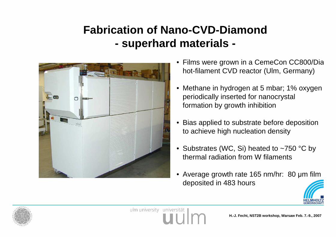
Fabrication of Nano-CVD-Diamond- superhard materials -
• Films were grown in a CemeCon CC800/Diahot-filament CVD reactor (Ulm, Germany)
• Methane in hydrogen at 5 mbar; 1% oxygenperiodically inserted for nanocrystalformation by growth inhibition
• Bias applied to substrate before depositionto achieve high nucleation density
• Substrates (WC, Si) heated to ~750 °C bythermal radiation from W filaments
• Average growth rate 165 nm/hr: 80 μm filmdeposited in 483 hours

H.-J. Fecht, NST2B workshop, Warsaw Feb. 7.-9., 2007
02468
101214161820222426
Sta
nd
ze
itin
Wo
ch
en
Hard metal TiN Ceramic Diamaze PSD
05
10152025303540455055606570
rel.
Sta
nd
ze
it
Hard metal Diamaze PSD
1
63
Applications: Life time of cutting tools (in weeks)
Plastics (Foil with nx-Ti-oxide)
Glass
150 Tests
Significant improvement of lifetime
H.-J. Fecht, NST2B workshop, Warsaw Feb. 7.-9., 2007
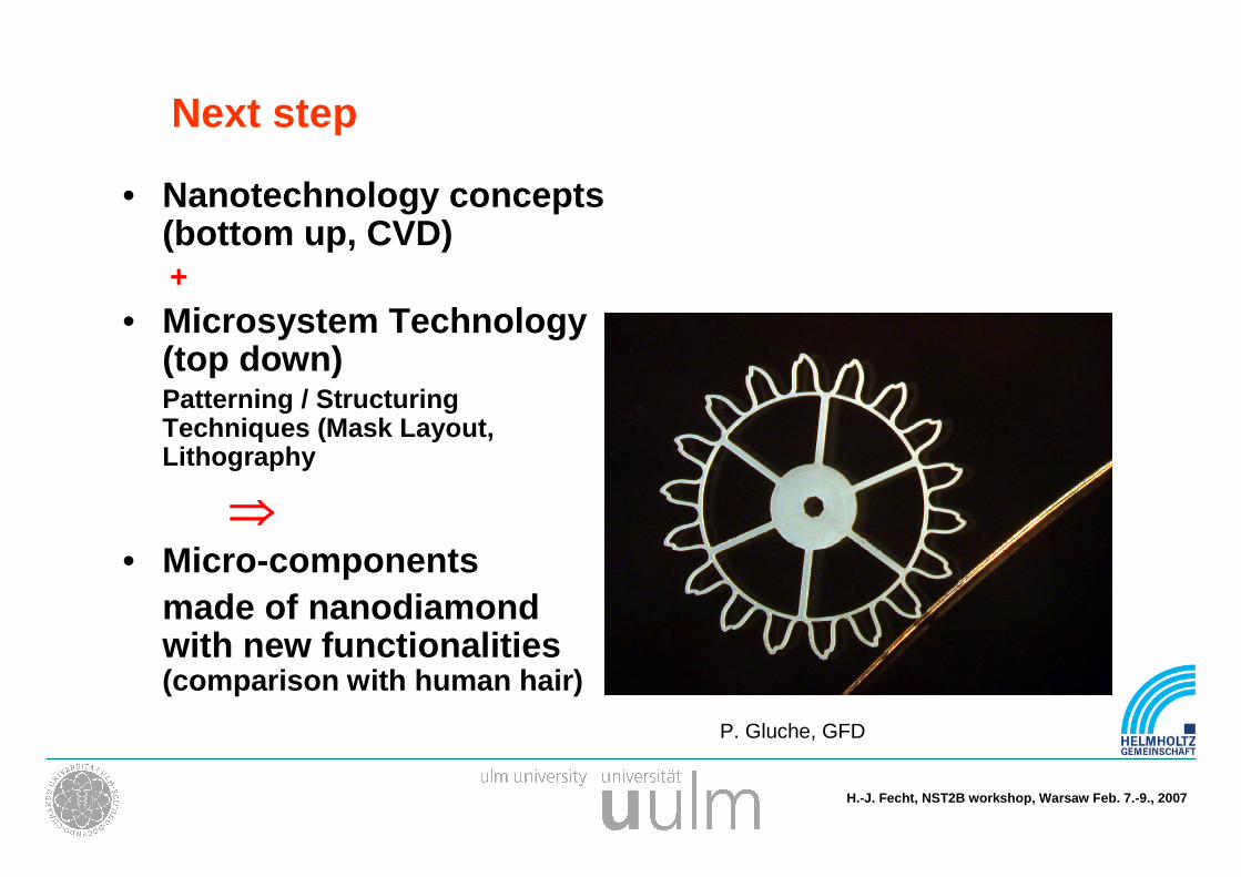
• Nanotechnology concepts(bottom up, CVD)+
• Microsystem Technology(top down)Patterning / StructuringTechniques (Mask Layout,Lithography
• Micro-components
made of nanodiamondwith new functionalities(comparison with human hair)
Next step
P. Gluche, GFD

H.-J. Fecht, NST2B workshop, Warsaw Feb. 7.-9., 2007
Diamond untreated
Oxygen(cell growth)
Hydrogen Fluorene(bacteria disappear)
Bio AspectSurface terminationCell growth, neurons
H.-J. Fecht, NST2B workshop, Warsaw Feb. 7.-9., 2007
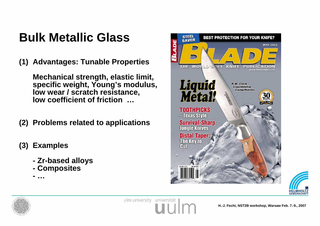
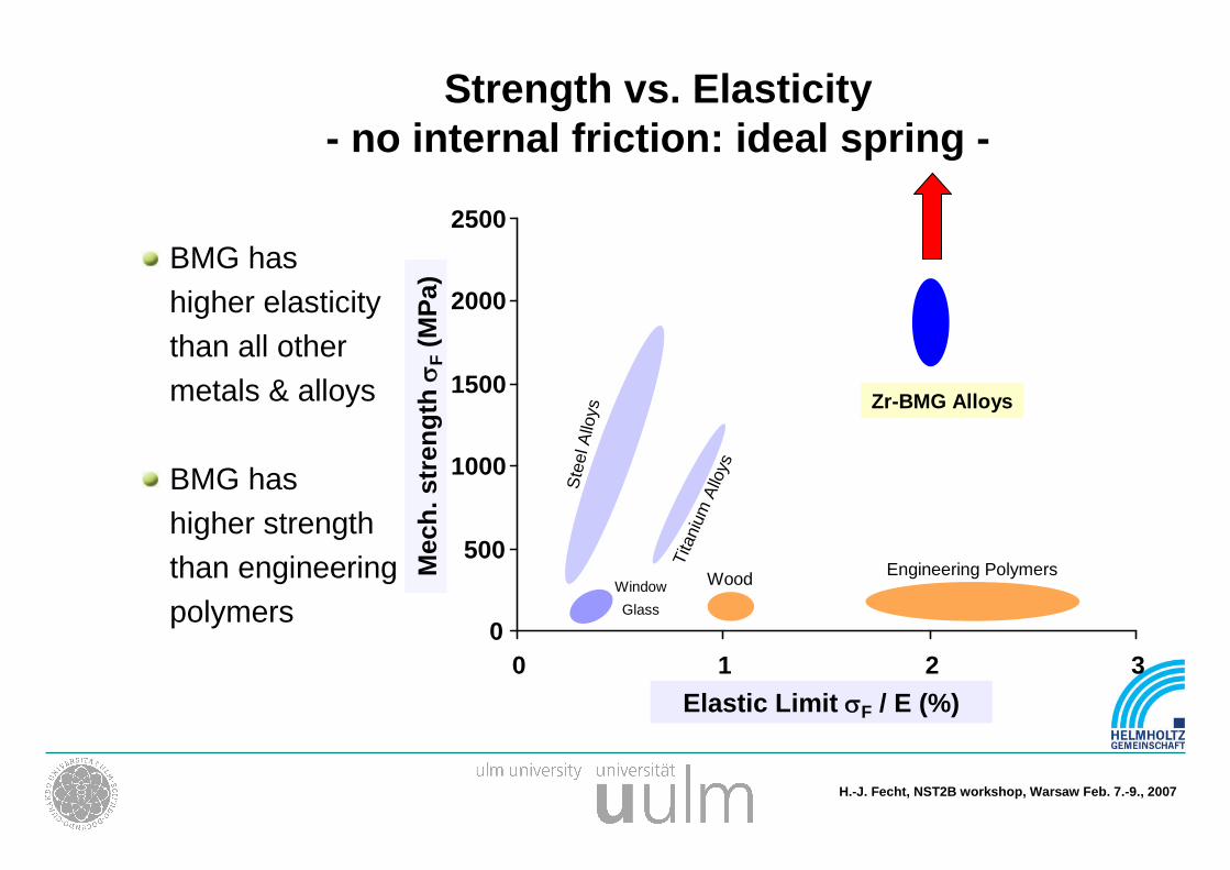
Bulk Metallic Glass
(1) Advantages: Tunable Properties
Mechanical strength, elastic limit,specific weight, Young’s modulus,low wear / scratch resistance,low coefficient of friction …
(2) Problems related to applications
(3) Examples
- Zr-based alloys- Composites- …
H.-J. Fecht, NST2B workshop, Warsaw Feb. 7.-9., 2007
0
500
1000
1500
2000
2500
0 1 2 3
Elastic Limit(%)
Engineering PolymersWoodWindow
Glass
Tita
niu
mA
lloys
Ste
el A
lloys
Zr-BMG Alloys
BMG has
higher elasticity
than all other
metals & alloys
BMG has
higher strength
than engineering
polymers
Strength vs. Elasticity- no internal friction: ideal spring -
Elastic Limit F / E (%)
Mech
.str
en
gth
F
(MP
a)
H.-J. Fecht, NST2B workshop, Warsaw Feb. 7.-9., 2007
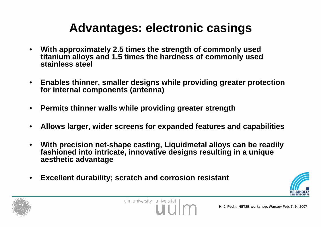
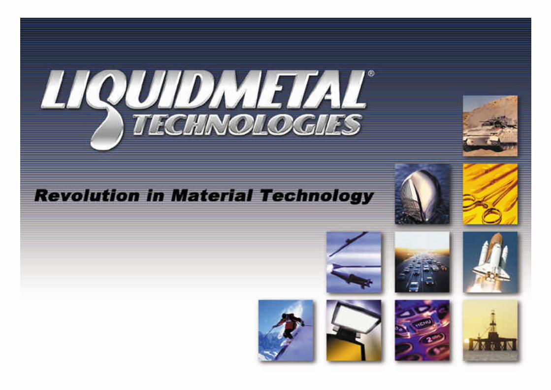
Advantages: electronic casings
• With approximately 2.5 times the strength of commonly usedtitanium alloys and 1.5 times the hardness of commonly usedstainless steel
• Enables thinner, smaller designs while providing greater protectionfor internal components (antenna)
• Permits thinner walls while providing greater strength
• Allows larger, wider screens for expanded features and capabilities
• With precision net-shape casting, Liquidmetal alloys can be readilyfashioned into intricate, innovative designs resulting in a uniqueaesthetic advantage
• Excellent durability; scratch and corrosion resistant
H.-J. Fecht, NST2B workshop, Warsaw Feb. 7.-9., 2007
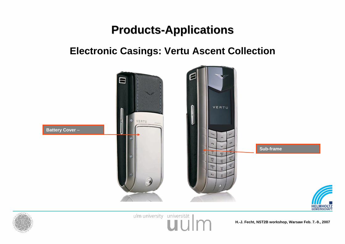
Battery Cover –
Sub-frame
Electronic Casings: Vertu Ascent Collection
ProductsProducts--ApplicationsApplications

H.-J. Fecht, NST2B workshop, Warsaw Feb. 7.-9., 2007
Liquidmetal Hinges
Precise Net-Shape Casting, High Reliability, Low Friction
Samsung SPHSPH--E3200E3200
H.-J. Fecht, NST2B workshop, Warsaw Feb. 7.-9., 2007
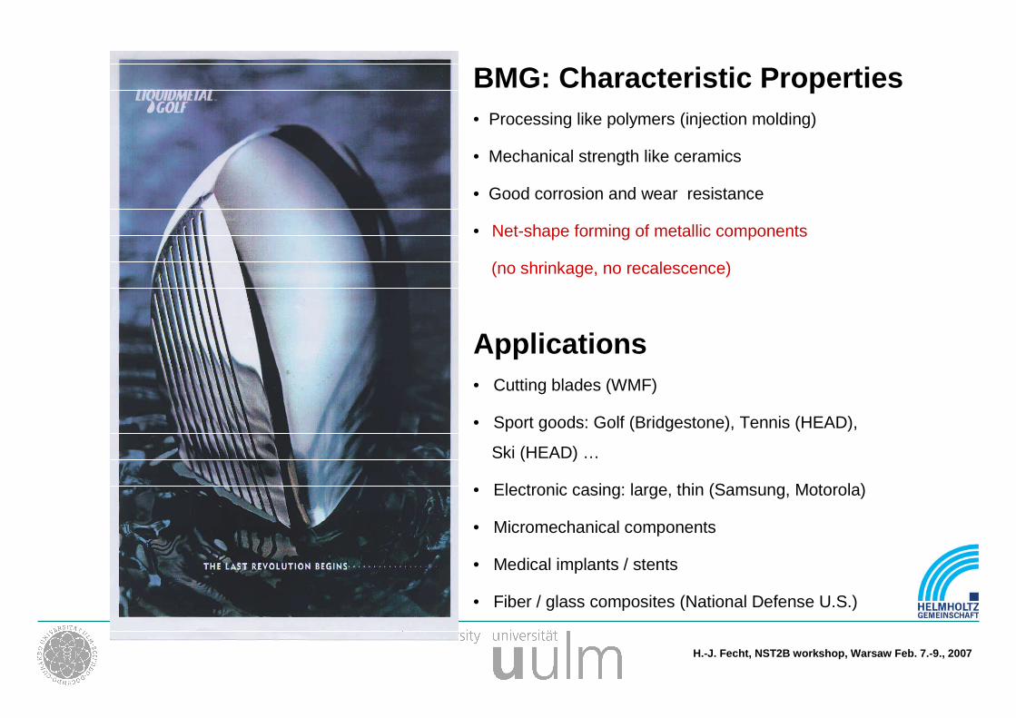
BMG: Characteristic Properties
• Processing like polymers (injection molding)
• Mechanical strength like ceramics
• Good corrosion and wear resistance
• Net-shape forming of metallic components
(no shrinkage, no recalescence)
Applications
• Cutting blades (WMF)
• Sport goods: Golf (Bridgestone), Tennis (HEAD),
Ski (HEAD) …
• Electronic casing: large, thin (Samsung, Motorola)
• Micromechanical components
• Medical implants / stents
• Fiber / glass composites (National Defense U.S.)
H.-J. Fecht, NST2B workshop, Warsaw Feb. 7.-9., 2007
Conclusion
NanoMaterialsplus
NanoToolsplus
a Product based on Nanotech
NanoEffects for the micro- and macroworld
H.-J. Fecht, NST2B workshop, Warsaw Feb. 7.-9., 2007
H.-J. Fecht, NST2B workshop, Warsaw Feb. 7.-9., 2007
Materials Innovation AwardGerman Engineering Foundation
- Thanks -
DFGLandesstiftung BW
GFD mbH
H.-J. Fecht, NST2B workshop, Warsaw Feb. 7.-9., 2007
- THANK YOU -for your kind attention

H.-J. Fecht, NST2B workshop, Warsaw Feb. 7.-9., 2007
Why does it work: public – private partnership
Academic know-how not existing in industry
Measurements not possible with that precision inindustry
Outsourcing of R&D in major companies
Reduction of risk for new projects with long lead times
Start-ups: receive funding through cooperative projects
…
H.-J. Fecht, NST2B workshop, Warsaw Feb. 7.-9., 2007
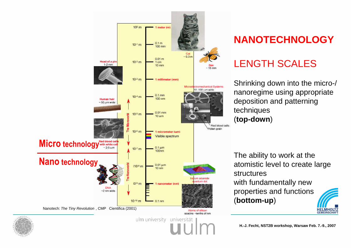
Micro technology
Nano technology
Nanotech: The Tiny Revolution , CMP Cientifica (2001)
NANOTECHNOLOGY
LENGTH SCALES
Shrinking down into the micro-/nanoregime using appropriatedeposition and patterningtechniques(top-down)
The ability to work at theatomistic level to create largestructureswith fundamentally newproperties and functions(bottom-up)

H.-J. Fecht, NST2B workshop, Warsaw Feb. 7.-9., 2007
Source: Microtechnology Innovation Team Deutsche Bank
Nanotechnology Market Segmentation
20002001200220032004
Other
Biotech
Nanomaterials
ToolsDevices
Electronics
0
50
100
150
200
250
300
Mark
et
Siz
e($
Billio
n)
Year
2002: 22.6 $ Bn2006: 32.4 $ Bn
H.-J. Fecht, NST2B workshop, Warsaw Feb. 7.-9., 2007
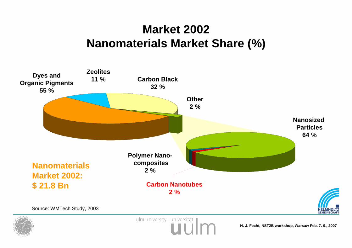
Market 2002Nanomaterials Market Share (%)
NanosizedParticles
64 %
Carbon Nanotubes2 %
NanomaterialsMarket 2002:$ 21.8 Bn
Other2 %
Carbon Black32 %
Dyes andOrganic Pigments
55 %
Zeolites11 %
Polymer Nano-composites
2 %
Source: WMTech Study, 2003

H.-J. Fecht, NST2B workshop, Warsaw Feb. 7.-9., 2007
Forecast 2006Nanomaterials Market Share (%)
Nanomaterials Market 2006:$ 28.8 Bn(increases by 7 % AAGRbetween 2002 and 2006)
CarbonNanotubes
38 %
Polymer Nano-composites
34 %
NanosizedPowders
28 %
Zeolites9 %
Other11 %
Dyes andOrganic Pigments
52 %
Carbon Black28 %
Source: WMTech Study, 2003
H.-J. Fecht, NST2B workshop, Warsaw Feb. 7.-9., 2007
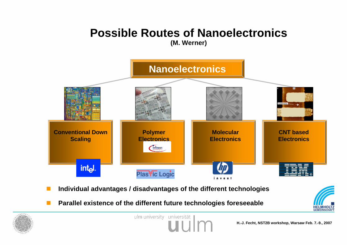
Possible Routes of Nanoelectronics(M. Werner)
Individual advantages / disadvantages of the different technologies
Parallel existence of the different future technologies foreseeable
Nanoelectronics
Conventional DownScaling
PolymerElectronics
MolecularElectronics
CNT basedElectronics
H.-J. Fecht, NST2B workshop, Warsaw Feb. 7.-9., 2007
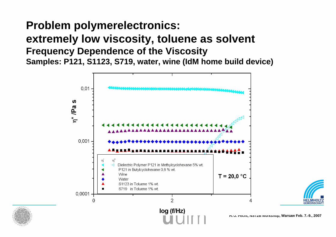
Problem polymerelectronics:extremely low viscosity, toluene as solventFrequency Dependence of the ViscositySamples: P121, S1123, S719, water, wine (IdM home build device)
H.-J. Fecht, NST2B workshop, Warsaw Feb. 7.-9., 2007
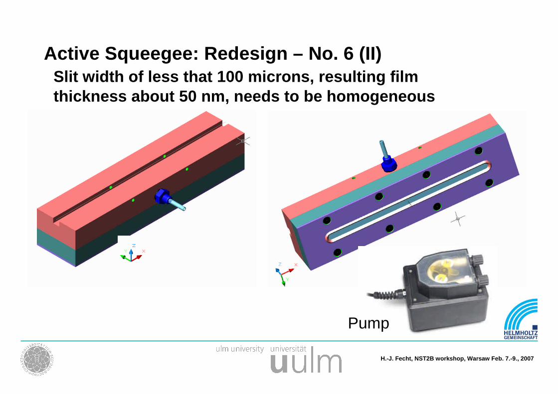
Active Squeegee: Redesign – No. 6 (II)Slit width of less that 100 microns, resulting filmthickness about 50 nm, needs to be homogeneous
Pump

H.-J. Fecht, NST2B workshop, Warsaw Feb. 7.-9., 2007
- NanoMaterials -Dimensionality and Fields of Application
• Catalysis
• Ferrofluids
• Composites with
increased el. conductivity
• Sensors / Actors
• Magnetoelectronics
• Reading / Writing
Heads
• Optical Applications
• Structural Nanomaterials
• Superplastic Ceramics
• Filter
• Hard Coatings
• Low temperature co-fired
ceramics (LTCC)Source: H. Hahn / INT
H.-J. Fecht, NST2B workshop, Warsaw Feb. 7.-9., 2007
Center of ExcellenceMicro and Nano MaterialsUniversität Ulm
WMtech
ProductionProcessingApplicationConsulting
Training

H.-J. Fecht, NST2B workshop, Warsaw Feb. 7.-9., 2007
Technology / Areas of competence WMtech
1. Development and Production of „New advanced Materials“
2. Development and improvement of production processing
3. Development of prototypes, sales of prototypes
4. Analysis, Simulation
5. Coordination, Technology transfer
6. Sales, marketing, licensing
H.-J. Fecht, NST2B workshop, Warsaw Feb. 7.-9., 2007
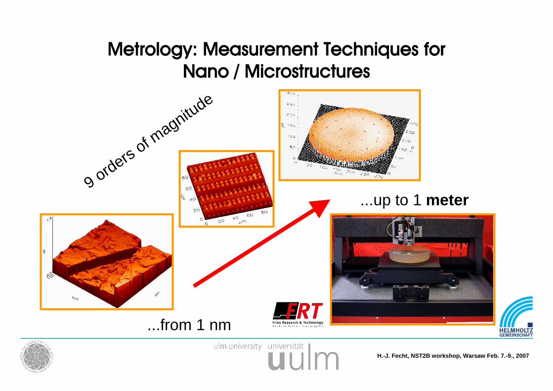
Metrology: Measurement Techniques forNano / Microstructures
...up to 1 meter9 ord
ersof magnitu
de
...from 1 nm
H.-J. Fecht, NST2B workshop, Warsaw Feb. 7.-9., 2007
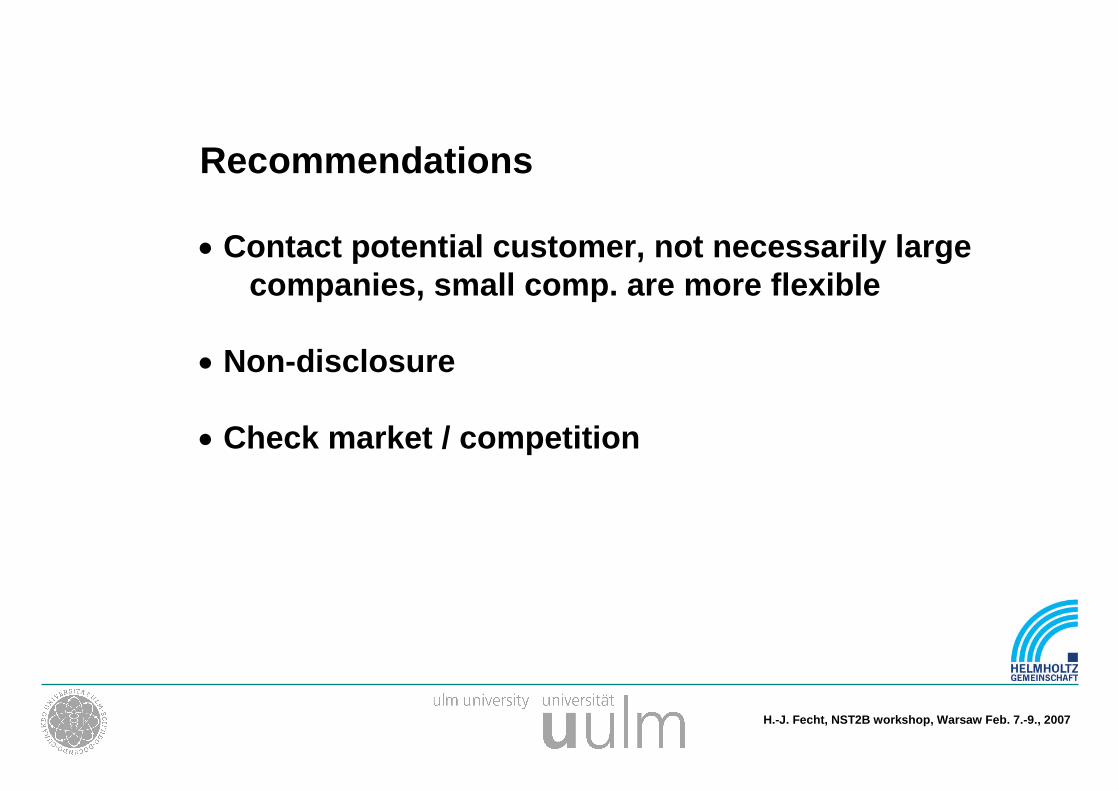
Recommendations
Contact potential customer, not necessarily largecompanies, small comp. are more flexible
Non-disclosure
Check market / competition