work sheet two
TRANSCRIPT

Chapter 5 Pipeline and vector processing
In this chapter 5-1 Parallel Processing 5-2 Pipelining 5-3 Arithmetic Pipeline 5-4 Instruction Pipeline 5-5 RISC Pipeline 5-6 Vector Processing 5-7 Array Processors 5-1 Parallel Processing Parallel processing is a term used to denote a large class of techniques that are used to provide simultaneous data-processing tasks for the purpose of increasing the computational speed of a computer system. Instead of processing each instruction sequentially as in a conventional computer, a parallel processing system is able to perform concurrent data processing to achieve faster execution time. For example, while an instruction is being executed in the ALU, the next instruction can be read from memory. The system may have two or more ALUs and be able to execute two or more instructions at the same time. Furthermore, the system may have two or more processors operating concurrently. The purpose of parallel processing is to speed up the computer processing capability and incense its throughput, that is, the amount of processing that can be accomplished during a given interval of time. The amount of hardware increases with parallel processing, and with it, the cost of the system increases. However, technological developments have reduced hardware costs to the point where parallel processing techniques are economically feasible. Parallel processing can be viewed from various levels of complexity. At the lowest level, we distinguish between parallel and serial operations by the type of registers used. Shift registers operate in serial fashion one bit at a time, while registers with parallel load operate with all the bits of the word simultaneously. Parallel processing at a higher level of complexity can be achieved by having a multiplicity of functional units that perform identical or different operations simultaneously. Parallel processing is established by distributing the data among the multiple functional units. For example, the arithmetic, logic, and shift operations can be separated into three units and the operands diverted to each unit under the supervision of a control unit. Figure 5-1 shows one possible way of separating the execution unit into eight functional units operating in parallel. The operands in the register are applied to one of the units depending on the operation specified by the instruction associated with the operands. The operation Performed in each functional unit is indicated in each block of the diagram. The adder and integer multiplier perform the arithmetic operations with integer numbers.
p.c
The floating-point operations are separated into three circuits operating in parallel. The logic, shift, and increment operations can be performed concurrently on different data. All units are

independent of each other, so one number can be shifted while another number is being incremented. A multifunctional organization is usually associated with a complex control unit to coordinate all the activities among the various components. There are a variety of ways that parallel processing can be classified. It can be considered from the internal organization of the Processors, from the interconnection structure between Processors, or from the flow of information through the system. One classification introduced by M. 1. Flynn considers the organization of a computer system by the number of instructions and data items that are manipulated simultaneously. The normal operation of a computer is to fetch instructions from memory and execute them in the processor. The sequence of instructions read from memory constitutes an instruction stream. The operations performed on the data in the processor constitute a data stream. Parallel processing may occur in the instruction stream, in the data stream, or in both. Flynn’s classification divides computers into four major groups as follows: Single instruction stream, single data stream (SISD) Single instruction stream, multiple data stream (SIMD) Multiple instruction stream, single data stream (MISD) Multiple instruction stream, multiple data stream (MIMD) SISD represents the organization of a single computer containing a control unit, a processor unit, and a memory unit. Instructions are executed sequentially and the system may or may not have internal parallel processing capabilities. Parallel processing in this case may be achieved by means of multiple functional units or by pipeline processing.
SIMD represents an organization that includes many processing units under the supervision of a common control unit. All processors receive the same instruction from the control unit but operate on different items of data. The shared memory unit must contain multiple modules so that it can communicate with all the processors simultaneously.
MISD structure is only of theoretical interest since no practical system has been constructed using this organization. MIMD organization refers to a computer system capable of processing several programs at the same time. Most multiprocessor and multicomputer systems can be classified in this category. Flynn’s classification depends on the distinction between the performance of the control unit and the data-processing unit. It emphasizes the behavioral characteristics of the computer system rather than its operational and structural interconnections. One type of parallel processing that does not fit Flynn's classification is pipelining. The only two categories used from this classification are SIMD array processors discussed in Sec. 5-7, and MIMD multiprocessors refer in Chap. 13. In this chapter we consider parallel processing under the following main topics: 1. Pipeline processing 2. Vector processing 3. Array processors pipeline processing is an implementation technique where arithmetic sub operations or the phases of a computer instruction cycle overlap in execution. Vector processing deals with computations involving large vectors and matrices. Array processors perform computations on large arrays of data. 5-2 Pipelining
Pipelining is a technique of decomposing a sequential process into sub operation with each sub process being executed in a special dedicated segment that operates concurrently with all other segments. A pipeline can be visualized as a collection of processing segments through which binary information flows. Each segment performs partial processing dedicated by the way the task is partitioned. The result obtained from the computation in each segment is transferred to the next segment in the pipeline. The final result is obtained after the data have passed through all segments. The name 'pipeline” implies a flow of information analogous to an industrial assembly line. It is characteristic of pipelines that several computations can be in progress in distinct segments at the same time. The overlapping of computation is made possible by association a register with each segment in the pipeline. The registers provide isolation between each segment so that each can operate on distinct data simultaneously.
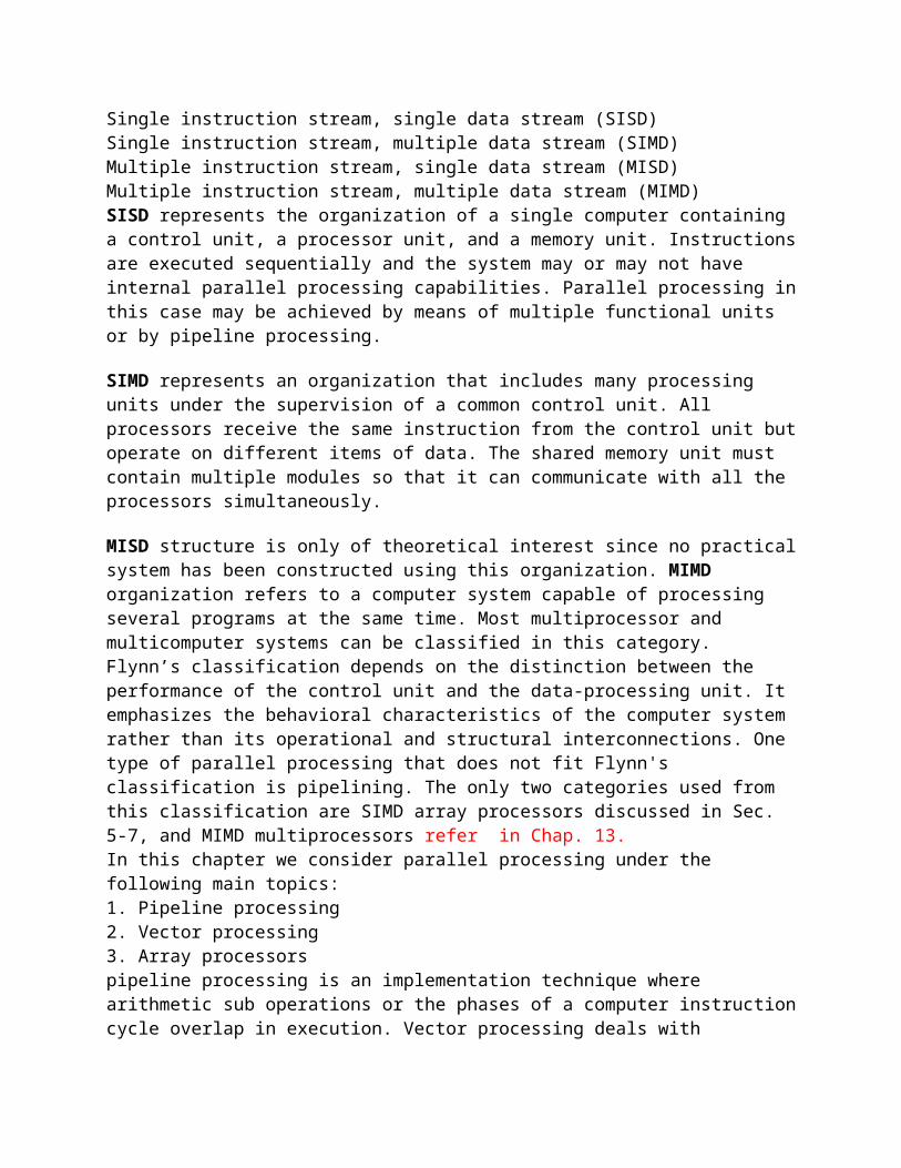
Perhaps the simplest way of viewing the pipeline structure is to imagine that each segment consists of an input resister followed by a combinational circuit. The register holds the data and the combinational circuit performs the sub operation in the particular segment. The output of the combinational circuit in a given segment is applied to the input register of the next segment. A clock is applied to all registers after enough time has elapsed to perform all segment activity. In this way the information flows through the pipeline one step at a time. The pipeline organization will be demonstrated by means of a simple example. Suppose that we want to perform the combined multiply and add operations with a stream of numbers. Ai * Bi + Ci for i= 1, 2, 3, . . . Each sub operation is to be implemented in a segment within a pipeline. Each segment has one or two registers and a combinational circuit as shown in Fig. 9-2. Ri through R5 are registers that receive new data with every clock pulse. The multiplier and adder are combinational circuits. The sub operations Performed in each segment of the pipeline are as follows: R1 Ai, R2 Bi Input Ai and BiR3R1 * R2, R4Ci Multiply and input Ci, R5 R3 + R4 Add C to product The five registers are loaded with new data every dock pulse. The effect of each clock is shown in Table 5-1. The first clock pulse transfers A1 and B1 into R 1 and R2.
Fig 5.2 example of pipeline processing

Table 5.1 content of registers in pipeline
The second clock pulse transfers the product of R1 and R2 into R3 and C1 into R4. The same clock pulse transfers A2 and B2 into RI and R2. The third clock pulse operates on all three segments simultaneously. It places A3 and B3 into RI and R2, transfers the product of R1 and R2 into R3, transfers C2 into R4, and places the sum of R3 and R4 into R5. It takes three dock pulses to fill up the pipe and retrieve the first output from R5. From there on, each dock produces a new output and moves the data one step down the pipeline. This happens as long as new input data flow into the system. When no more input data are available, the clock must continue until the last output emerges out of the pipeline. General Considerations any operation that can be decomposed into a sequence of sub operations of about the same complexity can be implemented by n pipeline processor. The technique is efficient for those applications that need to repeat the same task many times with different sets of data. The general structure of a four-segment pipeline is illustrated in Fig.5-3.
Fig 5.3 four segment pipeline
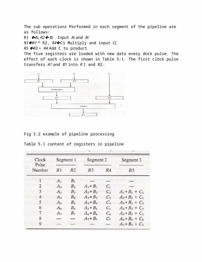
The operands pass through all four segments in a fixed sequence. Each segment consists of a combinational circuit S1 that performs sub operations over the data stream flowing through the pipe. The segments are separated by registers R that hold the intermediate results between the stages. Information flows between adjacent stages under the control of a common clock applied to all the registers simultaneously. We define a task as the total operation performed going through all the segments in the Pipeline. The behavior of a pipeline can be illustrated with a space-time diagram. This is a diagram that shows the segment utilization as a function of time. The space-time diagram of a four-segment pipeline is demonstrated in Fig. 5-4. The horizontal axis displays the time in dock cycles and the vertical axis gives the segment number. The diagram shows six tasks T1 through T6 executed in four segments. Initially, task T1 is handled by segment 1. After the first clock, segment 2 is busy with T1, while segment I is busy with task T2. Continuing in this manner, the first task T1 is completed after the fourth clock cycle. From then on, the pipe completes a task every clock cycle. No matter how many segments there are in the system, once the pipeline is full, it takes only one clock period to obtain an output. Now consider the case where a k-segment pipeline with a clock cycle time tp is used to execute n tasks. The first task T1 requires a time equal to kpt,, to complete its operation since there are k segments in the pipe. The remaining n — 1 tasks emerge from the pipe at the rate of one task per clock cycle and they will be completed after a time equal to (n — 1)t. Therefore, to complete n tasks using a k-segment pipeline requires k + (n — 1) clock cycles. For example pee, the diagram of Fig. 9-4 shows four segments and six tasks. The time required to complete all the operations is 4 + (6 — 1) 9 clock cycles, as indicated in the diagram. Next consider nonpipeline units that perform the same operation and takes a time equal to t 'o complete each task. The total time required for n tasks is ntn. The speedup of a pipeline processing over an equivalent nonpipeline processing is defined by the ratio
Fig 5 4 space time diagram
To duplicate the theoretical speed advantage of a pipeline process by means of multiple functional units, it is necessary to construct k identical units that will be operating in parallel. The implication is that a k-segment pipeline processor can be expected to equal the performance of k copies of an equivalent nonpipeline circuit under equal operating conditions. This is illustrated in Fig. 9-5, where four identical circuits are connected in parallel. Each P circuit performs the same task of an equivalent pipeline circuit. Instead of operating with the input data in sequence as in a pipeline, the parallel circuits accept four input data items simultaneously and perform four tasks at the same time. As far as the speed of operation is concerned, this is equivalent to a four segment pipeline. note that the four-unit circuit of Fig. 9-5 constitutes a single-instruction multiple-data (SIMD) organization since the same instruct tion is used to operate on multiple data in Parallel. There are various reasons why the Pipeline cannot operate at its maxim mum theoretical tate. Different segments may take different tines to complete their suboperation. The clock cycle must be chosen to equal the time delay of the segment with the maximum propagation time. This causes all other segments to waste time while waiting for the next clock. Moreover, it is not always

Fig 5.5 multiple functional units in parallel
correct to assume that a nonpipe circuit has the same time delay as that of an equivalent pipeline circuit. Many of the intermediate registers will not be needed in a single-unit circuit. Which can usually be constructed entirely as a combinatorial circuit. Nevertheless, the pipeline technique provides a faster operation over a purely serial sequence even though the maximum theoretical speed is never fully achieved. There are two areas of computer design where the pipeline organization is applicable. An arithmetic pipe line divides an arithmetic operation into sub- operations for execution in the pipeline segments. An instruction pipeline operates on a stream of instructions by overlapping the fetch, decode, and execute phases of the instruction cycle. The two types of pipelines are explained in the following sections.
5-3 Arithmetic Pipeline Pipeline arithmetic units are usually found in very high speed computers. They are used to implement floating-point operntions1 multiplication of fixed-point numbers, and similar computations encountered in scientific problems. A pipeline multiplier is essentially an array multiplier as described in chapter 10, Fig. 10-10 refer, with special adders designed to minimize the carry propagation time through the partial products. Floating-point operations are easily decomposed into sub operations as demonstrated in sec. 10-5. We will now show an example of a pipeline unit for floating-point addition and subtraction. The inputs to the floating-point adder pipeline are two normalized floating-point binary numbers.

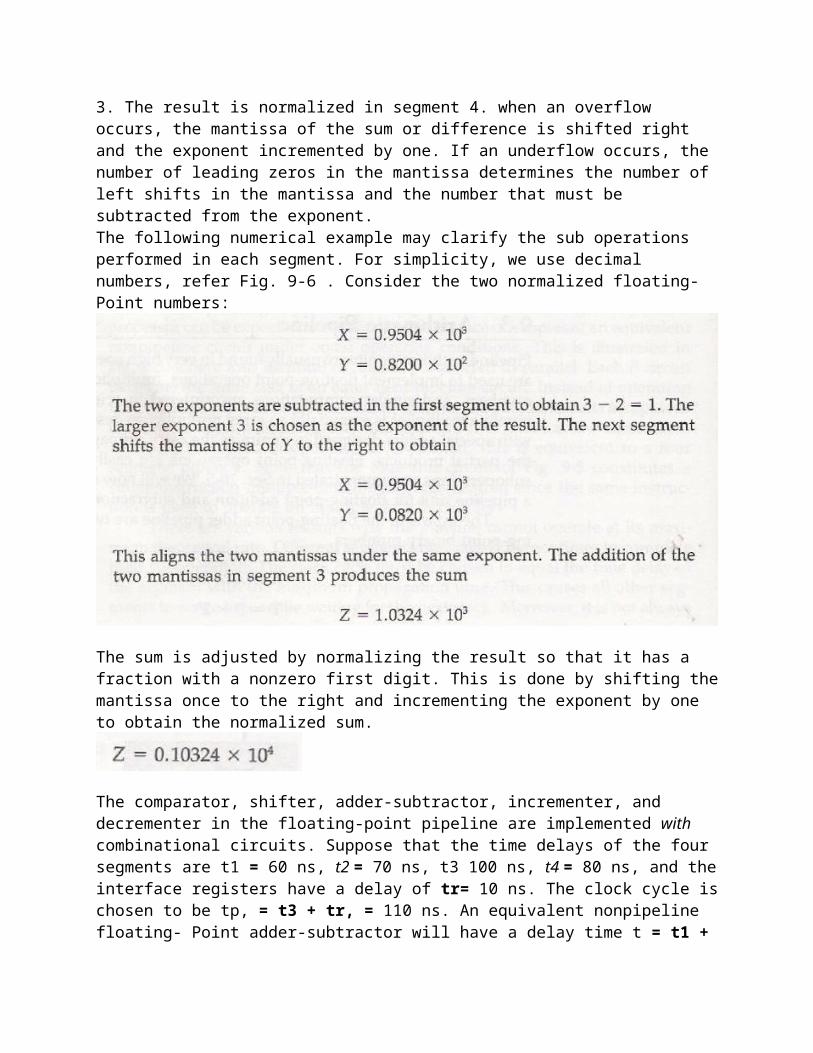
A and B are two fractions that represent the mantissas and a and b are the exponents. The floating-point addition and subtraction can be performed in four segments, as shown in Fig. 9-6. The registers labeled R are placed between the segments to store intermediate results. The sub operations that are performed in the four segments are: 1. Compare the exponents. 2. Align the mantissas. 3. Add or subtract the mantissas. 4. Normalize the result. This follows the procedure outlined in the flowchart of Fig. 10-15 but with some variations that are used to reduce the execution time of the sub operations. The exponents are compared by subtracting them to determine their difference. The larger exponent is chosen as the exponent of the result. The exponent difference determines how many times the mantissa associated with the smaller exponent must be shifted to the right. This produces an alignment of the two mantissas. It should be noted that the shift must be designed as a combinational circuit to reduce the shift time. The two mantissas are added or subtracted in segment 3. The result is normalized in segment 4. when an overflow occurs, the mantissa of the sum or difference is shifted right and the exponent incremented by one. If an underflow occurs, the number of leading zeros in the mantissa determines the number of left shifts in the mantissa and the number that must be subtracted from the exponent. The following numerical example may clarify the sub operations performed in each segment. For simplicity, we use decimal numbers, refer Fig. 9-6 . Consider the two normalized floating-Point numbers:
The sum is adjusted by normalizing the result so that it has a fraction with a nonzero first digit. This is done by shifting the mantissa once to the right and incrementing the exponent by one to obtain the normalized sum.

The comparator, shifter, adder-subtractor, incrementer, and decrementer in the floating-point pipeline are implemented with combinational circuits. Suppose that the time delays of the four segments are t1 = 60 ns, t2 = 70 ns, t3 100 ns, t4 = 80 ns, and the interface registers have a delay of tr= 10 ns. The clock cycle is chosen to be tp, = t3 + tr, = 110 ns. An equivalent nonpipeline floating- Point adder-subtractor will have a delay time t = t1 + t2 + t3 + 14 + tr, = 320 ns. In this case the pipelined adder has a speedup of 32o/110 = 2.9 over the nonpipelined adder.
5.4 Instruction Pipeline Pipeline processing can occur not only in the data stream but in the instruction stream as well. An instruction pipeline reads consecutive instructions from memory while previous instructions are being executed in other segments. This causes the instruction fetch and execute phases to overlap and perform simultaneous operations. One Possible digression associated with such a scheme is that an instruction may cause a branch out of sequence. In that case the pipeline must be emptied and all the instructions that have been read from memory after the branch instruction must be discarded. Consider a computer with an instruction fetch unit and an instruction execution unit designed to provide a two-segment pipeline. The instruction fetch segment can be implemented by means of a first-in, first-out (FIFO) buffer. This is a type of unit that forms a queue rather than a stack. Whenever the execution unit is not using memory, the control increments the program counter and uses its address value to read consecutive instructions from memory. The instructions are inserted into the FIFO buffer so that they can be executed on a first-in, first-out basis. Thus an instruction stream can be placed in a queue, waiting for decoding and processing by the execution segment. The instruction stream queuing mechanism provides an efficient way for reducing the average access time to memory for reading instructions. Whenever there is space in the FIFO buffer, the control unit initiates the next instruction fetch phase. The buffer acts as a queue from which control then extracts the instructions for the execution unit. Computers with complex instructions require other Phases in addition to the fetch and execute to process an instruction completely. In the most general case, the computer needs to process each instruction with the following sequence of steps.
1. Fetch the instruction from memory. 2. Decode the instruction. 3. Calculate the effective address. 4, Fetch the operands from memory. 5. Execute the instruction. 6. Store the result in the Proper place. There are certain difficulties that will prevent the instruction pipeline from operating at its maximum rate. Different segments may take different times to operate on the incoming information. Some segments are skipped for certain operations. For example, a register mode instruction does not need an effective address calculation. Two or more segments may require memory access at the same time, causing one segment to wait until another is finished with the memory. Memory access conflicts are sometimes resolved by using two memory buses for accessing instructions and data in separate modules. In this way, an instruction word and a data word can be read simultaneously from two different modules. The design of an instruction pipeline will be most efficient if the instruction cycle is divided into segments of equal duration. The time that each step takes to fulfill its function depends on the
instruction and the way it is executed. Example: Four-Segment Instruction Pipeline Assume that the decoding of the instruction can be combined with the calculation of the effective address into one segment. Assume further that most of the instructions place the result into a processor registers so that the instruction execution and storing of the result can be combined into one segment. This reduces the instruction pipeline into four segments. Figure 5-7 refer the book, shows how the instruction cycle in the CPU can be processed with a four-segment Pipeline. While an instruction is being executed in segment 4, the next instruction in sequence is busy fetching an operand from memory in segment 3. The effective address may be calculated in a separate arithmetic circuit for the third instruction, and whenever the memory is available, the fourth and all subsequent instructions can be fetched and Placed in an instruction FTFO. Thus up to four sub operations in the instruction cycle can overlap and up to four different instructions can be in progress of being processed at the same time. Once in a while, an instruction in the sequence may be a program control type that causes a branch out of normal sequence. In that case the Pending operations in the last two segments are completed and all information stored in the instruction buffer is deleted. The pipeline then restarts from the new address stored in the program counter. Similarly, an interrupt request, when acknowledged, will cause the pipeline to empty and start again from a new address value.
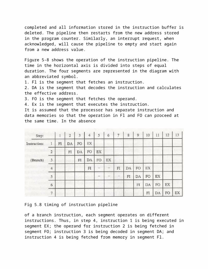
Figure 5-8 shows the operation of the instruction pipeline. The time in the horizontal axis is divided into steps of equal duration. The four segments are represented in the diagram with an abbreviated symbol. 1. Fl is the segment that fetches an instruction. 2. DA is the segment that decodes the instruction and calculates the effective address. 3. FO is the segment that fetches the operand. 4. Ex is the segment that executes the instruction. It is assumed that the processor has separate instruction and data memories so that the operation in Fl and FO can proceed at the same time. In the absence
Fig 5.8 timing of instruction pipeline
of a branch instruction, each segment operates on different instructions. Thus, in step 4, instruction 1 is being executed in segment EX; the operand for instruction 2 is being fetched in segment FO; instruction 3 is being decoded in segment DA; and instruction 4 is being fetched from memory in segment Fl. Assume now that instruction 3 is a branch instruction. As soon as this instruction is decoded in segment DA in step 4, the transfer from Fl to DA of the other instructions is halted until the branch instruction is executed in step 6. If the branch is taken, a new instruction is fetched in step 7. If the branch is not taken, the instruction fetched Previously in step 4 can be used. The pipeline then continues until a new branch instruction is encountered. Another delay may occur in the pipeline if the Ex segment needs to store the result of the operation in the data memory while the FO segment needs to fetch an operand. In that case, segment FO must wait until segment EX has finished its operation. In general, there are three major difficulties that cause the instruction pipeline to deviate from its normal operation. 1. Resource conflicts caused by access to memory by two segments at the same time. Most of these conflicts can be resolved by using separate instruction and data memories. 2. Data dependency conflicts arise when an instruction depends on the result of a previous instruction, but this result is not yet available. 3. Branch difficulties arise from branch and other instructions that change the value of PC. Data Dependency A difficulty that may caused a degradation of performance in an instruction pipeline is due to possible collision of data or address. A collision occurs when an instruction cannot proceed because previous instructions did not complete certain operations. A data dependency occurs when an instruction needs data that are not yet available. For example, an instruction in the FO segment may need to fetch an operand that is being generated at the same time by the previous instruction in segment EX. Therefore, the second instruction must wait for data to become available by the first instruction. Similarly, an address dependency may occur when an operand address cannot be calculated because the information needed by the addressing mode is not available. For example, an instruction with register indirect mode cannot proceed to fetch the operand if the previous instruction is loading the address into the register. Therefore, the operand access to memory must be delayed until the required address is available. Pipelined computers deal with such conflicts between data dependencies in a variety of ways. The most straightforward method is to insert hardware interlocks. An interlock is a circuit that detects instructions whose source operands are destination of instructions farther up in the pipeline. Detection of this situation causes the instruction whose source is not available to be delayed by enough clock cycles to resolve the conflict. This approach maintains the program sequence by using hardware to insert the required delays. Another technique called operand forwarding uses special hardware to detect a conflict and then avoid it by routing the data through special paths between pipeline segments. For example, instead of transferring an ALU result into a destination register, the hardware checks the destination operand, and if it is needed as a source in the next instruction, it passes the result directly into the ALU input, bypassing the register file. This method requires additional hardware paths through multiplexers as well as the circuit that detects the conflict. A procedure employed in some computers is to give the responsibility for solving data conflicts problems to the compiler that translates the high-level programming language into a machine
language Program. The compiler for such computers is designed to detect a data conflict and reorder the instruction as necessary to delay the loading of the conflicting data by inserting no-operation instructions. This method is referred to as delayed load. An example of delayed load is presented in the next section.
Handling of Branch instructions One of the major problems in operating an instruction Pipeline is the occurrence of branch instructions. A branch instruction can be conditional or unconditional.. An unconditional branch always alters the sequential program flow by loading the program counter with the target address. In a conditional branch, the control selects the target instruction if the condition is satisfied or the next sequential instruction if the condition is not satisfied. As mentioned previously, the branch instruction breaks the normal sequence of the instruction stream, causing difficulties in the operation of the instruction pipeline.
Pipelined computers employ various hardware techniques to minimize the performance degradation caused by instruction branching. One way of handling a conditional branch is to prefetch the target instruction in addition to the instruction following the branch. Both are saved until the branch is executed. If the branch condition is successful, the pipeline continues from the branch target instruction. An extension of this procedure is to continue fetching instructions from both places until the branch decision is made. At that time control chooses the instruction stream of the correct program flow. Another possibility is the use of a branch target buffer or BTB. The BTB is an associative memory (see sec. 12-4) included in the fetch segment of the pipeline. Each entry in the BTB consists of the address of a previously executed branch instruction and the target instruction for that branch. It also stores the next few instructions after the branch target instruction. When the pipeline decodes a branch instruction, it searches the associative memory BTB for the address of the instruction. If it is in the BTB, the instruction is available directly and prefetch continues from the new path. If the instruction is not in the BTB, the pipeline shifts to a new instruction stream and stores the target instruction in the BTB. The advantage of this scheme is that branch instructions that have occurred previously are readily available in the pipeline without interruption. A variation of the BTB is the loop buffer, This is a small very high speed register file maintained by the instruction fetch segment of the pipeline. When a program loop is detected in the program, it is stored in the loop buffer in its entirety, including all branches. The program loop can be executed directly without having to accesses memory until the loop mode is removed by the final branching out. Another procedure that some computers use is branch prediction. A pipeline with branch prediction uses some additional logic to guess the outcome of a conditional branch instruction before it is executed. The pipeline then begins prefetching the instruction stream from the predicted path. A correct prediction eliminates the wasted time caused by branch penalties. A procedure employed in most RISC processors is tie delayed branch. In this procedure, the compiler detects the branch instructions and rearranges the machine language code sequence by inserting useful instructions that keep the pipeline operating without interruptions. An example of delayed branch is the insertion of a no-operating instruction after a branch instruction. This causes the computer to fetch the target instruction during the execution of the no- operation instruction, allowing a Continuous flow of the pipeline. An example of delayed branch is
presented in the next section. 5-5 RISC Pipeline The reduced instruction set computer (RISC) was introduced in Sec. s-8. Among the characteristics attributed to RISC is its ability to use an efficient instruction pipeline. The simplicity of the instruction set can be utilized to implement an instruction pipeline using a small number of sub operations, with each being executed in one clock cycle. Because of the fixed-length instruction format, the decoding of the operation can occur at the same time as the register selection. All data manipulation instructions have register-to- register operations. Since all operands are in registers, there is no need for calculating an effective address or fetching of operands from memory. Therefore, the instruction Pipeline can be implemented with two or three segments. One segment fetches the instruction from program memory, and the other segment executes the instruction in the ALU. A third segment may be used to store the result of the ALU operation in a destination register. The data transfer instructions in RISC are limited to load and store instructions. These instructions use register indirect addressing. They usually need three or four stages in the pipeline. To prevent conflicts between a memory access to fetch an instruction and to load or store an operand, most RISC machines use two separate buses with two memories: one for storing the instructions and the other for storing the data. The two memories can some time operate at the same speed as the CPU clock and are referred to as cache memories (see Sec. 12-5). As mentioned in Sec. 8-8, one of the major advantages of RISC is its ability to execute instructions at the rate of one Per clock cycle. It is not possible to expect that every instruction be fetched from memory and executed in one clock cycle. What is done, in effect, is to start each instruction with each clock cycle and to pipeline the processor to achieve the goal of single-cycle instruction execution. The advantage of RISC over CISC (complex instruction set computer) is that RISC can achieve pipeline segments, requiring just one clock cycle, while CISC uses many segments in its pipeline, with the longest segment requiring two or more clock cycles. Another characteristic of RISC is the support given by the compiler that translates the high-level language program into machine language Program. Instead of designing hardware to handle the difficulties associated with data conflicts and branch penalties, RISC processors rely on the efficiency of the compiler to detect and minimize the delays encountered with these problems. The following examples show how a compiler can optimize the machine language program to compensate for pipeline conflicts.
Example: Three-Segment Instruction Pipeline A typical set of instructions for a RISC processor are listed in Table 8-12. We see from this table that there are three types of instructions. The data manipulation instructions operate on data in processor registers. The data transfer instructions are load and store instructions that use an effective address obtain from the addition of the contents of two registers or a register and a displacement constant provided in the instruction. The program control institutions use register values and a constant to evaluate the branch address, which is transferred to a register or the program counter PC.
Now consider the hardware operation for such a computer. The control section fetches the instruction from program memory into an instruction register. The instruction is decoded at the same time that the registers needed for the execution of the instruction are selected. The
processor unit consists of a number of registers and an arithmetic logic unit (ALU) that performs the necessary arithmetic, logic and shift operations. A data memory is used to load or store the data from a selected register in the register file. The instruction cycle can be divided into three sub operations and implemented in three segments: I: Instruction fetch A: ALU operation E: Execute instruction The I segment fetches the instruction from program memory. The instruction is decoded and an ALU operation is performed in the A segment. The ALU is used for three different functions, appending on the decoded instruction. It performs an operation for a data manipulation instruction, it evaluates the effective address for a load or store instruction, or it calculates the brand address for a program control instruction. The E segment directs the output of the ALU to one of three destinations, depending on the decoded instruction. It transfers the result of the ALU operation into a destination register in the register file, it transfers the effective address to a data memory for loading o storing, or it transfers the branch address to the program counter. Delayed Load Consider now the operation of the following four instructions: 1. LOAD: R1 M[address l] 2. LOAD: R2M[address 2] 3. ADD: R3R1 + R2
4. STORE: M[address 3]R3
If the three-segment pipeline proceeds without interruptions, there will be a data conflict in instruction 3 because the operand in R2 is not yet available in the A segment. This can be seen from the timing of the pipeline shown in Fig. 5-9(a). The E segment in clock cycle 4 is in a process of placing the memory data into R2. The A segment in clock cycle 4 is using the data from R2, but the value in R2 will not be the correct value since it has not yet been transferred from memory. It is up to the compiler to make sure that the instruction following the load instruction uses the data fetched from memory. If the compiler cannot find a useful instruction to put after the load, it inserts a no-op (no-operation) instruction. This is a type of instruction that is fetched from memory but has no operation, thus wasting a dock cycle. This concept of delaying the use of the data loaded from memory is referred to as delayed load. Figure 5-9(b) shows the same program with a no-op instruction inserted after the load to R2 instruction. The data is loaded into R2 in clock cycle 4. The add instruction uses the value of R2 in step 5. Thus the no-op instruction is used to advance one clock cycle in order to compensate for the data conflict in the pipeline. (Note that no operation is performed in segment A during clock cycle 4 or segment E during dock cycle 5.) The advantage of the delayed load approach is that the data dependency is taken care of by the compiler rather than the hardware. This results in simpler hardware segment since the segment does not have to check if the content of the register being accessed is currently valid or not.

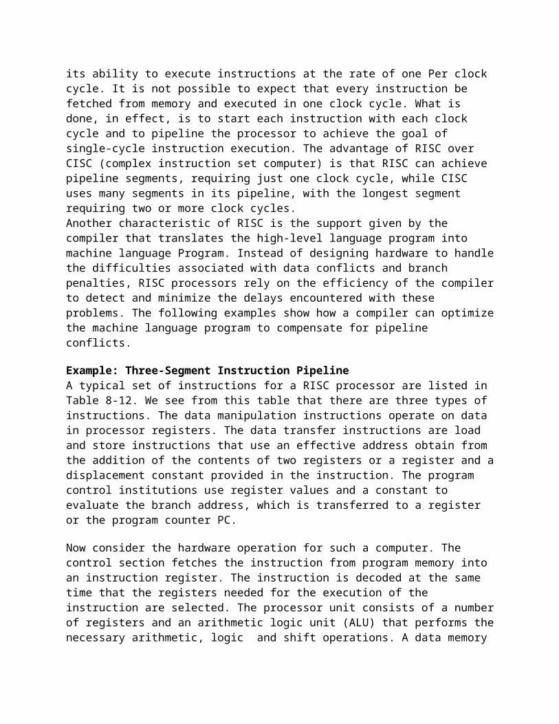
Delayed Branch It was shown in Fig. 9-8 that a branch instruction delays the Pipeline operation until the instruction at the branch address is fetched. Several techniques for reducing branch penalties were discussed in the preceding section. The method used in most RISC Processors is to rely on the compiler to redefine the branches so that they take effect at the proper time in the Pipeline. This method is referred to as delayed branch.
The compiler for a Processor that uses delayed branches is designed to analyze the instructions before and after the branch and rearrange the program sequence by inserting useful instructions in the delay steps. For example, the compiler can determine that the program dependencies allow one or more instructions preceding the branch to be moved into the delay steps after the branch. These instructions are then retched from memory and executed through the pipeline while the branch instruction is being executed in other segments. The effect is the same as if the instructions were executed in their original order, except that the branch delay is removed. It is up to the compiler to find useful instructions to put after the branch instruction. Failing that, the compiler can insert no-op instructions. An example of delayed branch is shown in Fig. 9-10. The program for this example consists of five instructions: Load from memory to R1 Increment R2 Add R3 to R4 Subtract R5 from R6 Branch to address X In Fig. 9-10 (a) below, the compiler inserts two no-op instructions after the branch. The branch address X is transferred to PC in clock cycle 7. The fetching of the instruction at X is delayed by two clock cycles by the no-op instructions. The instruction at X starts the fetch Phase at clock cycle 8 after the program counter PC has been updated. The program in Fig. 9-10(b) is rearranged by placing the add and subtract instructions after the

branch instruction instead of before as in the original Program. Inspection of the pipeline timing shows that PC is updated to the value of X in dock cycle 5, but the add and subtract instructions are fetched from memory and executed in the Proper sequence. In other words, if the load instruction is at address 1o1 and x is equal to 350, the branch instruction is fetched from address 103. The add instruction is fetched from address 104 and executed in clock cycle 6. The subtract instruction is fetched from address 105 and executed in clock cycle 7. Since the value of X is transferred to PC with clock cycle 5 in the E segment, the instruction fetched from memory at clock cycle 6 is from address 350, which is the instruction at the branch address.
Fig example of delayed branch
5-6 Vectors Processing There is a class of computational problems that are beyond the capabilities of a conventional computer. These problems are characterized by the fact that they require a vast number of computations that will take a conventional computer days or even weeks to complete. In many science and engineering applications, the problems can be formulated in terms of vectors and matrices that lend themselves to vector processing. Computers with vector processing capabilities are in demand in specialized applications. The following are representative application areas where vector processing is of the utmost importance. Long-range weather forecasting Petroleum explorations Seismic data analysis Medical diagnosis Aerodynamics and space flight simulations

Artificial intelligence and expert systems mapping the human genome Image processing
Without sophisticated computers, many of the required computations cannot be completed within a reasonable amount of time. To achieve the required level of high performance it is necessary to utilize the fastest and most reliable hardware and apply innovative procedures from vector and parallel processing techniques. Vector Operations Many scientific problems require arithmetic operations on large arrays of numbers. These numbers are usually formulated as vectors and matrices of floating-point numbers. A vector is an ordered set of a one-dimensional array of data items. A vector V of length n is represented as a row vector by V = (V1, V2, V3,…….Vn) It may be represented as a column vector if the data items are listed in a column. A conventional sequential computer is capable of processing operands one at a time. Consequently, operations on vectors must be broken down into single computations with subscripted variables. The element V of vector V is written as V(i) and the index i refers to a memory address or register where the number is stored. To examine the difference between a conventional scalar processor and a vector processor, consider the following Fortran DO loop: DO 20 I= 1, 100 20 c(I)=B(I)+A(I) This is a program for adding two vectors A and B of length 100 to produce a vector C. This is implemented in machine language by the following sequence of operations. Initial1ze I = 0 20 Read A(I) Read B(I) Store C(I) = A(I) + B(I) Increment I = I + I If I<=100 go to 20? Continue This constitutes a program loop that reads a pair of operands from arrays A and B arid performs a floating-point addition. The Loop control variable is then updated and the steps repeat 100 times.
A computer capable to vector processing eliminates the overhead associated with the time it takes to fetch and execute the instructions in the program loop. It allows operations to be specified with a single vector instruction of the form C(i:100) = A(1:100) + B(1:100) The vector instruction includes the initial address of the operands, the length of the vectors, and the operation to be performed, all in one composite instruction. The addition is done with a pipelined floating-point adder similar to the one shown in Fig. 5-6.
A possible instruction format for a vector instruction is shown in Fig. 9-11. This is essentially a

three-address instruction with three fields specifying the base address of the operands and an additional field that gives the length of the data items in the vectors. This assumes that the vector operands reside in memory. It is also possible to design the processor with a large number of registers and store all operands in registers prior to the addition operation. In that case the base address and length in the vector instruction specify a group of CPU registers. Matrix Multiplication Matrix multiplication is one of the most computational intensive operations performed in computers with vector processors. The multiplication of two n x n matrices consists of n2 inner products or n' multiply—add operations. An n x m matrix of numbers has n rows and m columns and may be considered as constituting a set of n row vectors or a set of n column vectors. Consider, for example, the multiplication of two 3 x 3 matrices A and B.
This requires three multiplications and (after initializing c11 to 0) three addition.. The total number of multiplications or additions required to compute the matrix product is 9 X 3 =27. If we consider the linked multiply—add operation c + a x b as a cumulative operation, the product of two n x n matrices requires n3 multiply—add operations. The computation consists of n2 inner products, with each inner product requiring n multiply—add operations assuming that c is initialized tm zero before computing each element in the product matrix. In general, the inner product consists of the sum of k product terms of the form C = A1B1, + A2B2 + A3B3, + A4B4 + ... + Ak,Bk In a typical application k may be equal to 100 or even 1000. The inner product calculation on a pipeline vector processor is shown in Fig. 5-12. The values of A and B are either in memory or in processor registers. The floating-point multiplier pipeline and the floating-point adder pipeline are assumed to have four segments each. All segment registers in the multiplier and adder are initialized to 0. Therefore, the output of the adder is 0 for the first eight cycles until both pipes are full. Ai and Bi pairs are brought in and multiplied at a rate of one pair per cycle. after the first four cycles, the products begin to be added to the output of the adder. During the next four cycles 0 is added to the products interring the adder pipeline. At the end of the eighth cycle, the first four products A1 B1 through A4 B4 are in the four adder , and the next four products, A5 B5 through A8 B8, are in the multiplier segments. At the beginning of the ninth cycle, the output of
the adder is A1 B1 and the output of the multiplier is A5 B5. Thus the ninth cycle starts the addition A1 B1 + r5 B5 in the adder pipeline. The tenth cycle starts the addition A2 B2 + A6 Bb, and so on. This pattern breaks down the summation into four sections as follows:
Fig 5.12 Multiplier Adder pipeline
When there are no more product terms to be added, the system inserts four zeros into the multiplier pipeline. The adder pipeline will then have one partial product in each of its four segments, corresponding to the four sums listed in the four rows in the above equation. The four partial sums are then added to form the final sum. Memory interleaving Pipeline and vector processors often require simultaneous access to memory from two or more sources. An instruction Pipeline may require the fetching of an instruction and an operand at the same time from two different segments Similarly, an arithmetic pipeline usually requires two or more operands to enter the pipeline at the same time. Instead of using two memory buses for simultaneous access, the memory can be partitioned into a number of modules connected to a common memory address and data buses. A memory module is a memory array together with its own address and data registers. Figure 9-13 shows a memory unit with four modules. Each memory array has its own address register AR and data register DR. The address registers receive information from a common address bus and the data registers communicate with a bidirectional data bus. The two least significant bits of the address can be used to distinguish between the four modules. The modular system permits one module to initiate a memory access while other modules are in the process of reading or writing a word and each module can honor a memory request independent of the state of the other modules.

Fig multiple module memory organization
The advantage of a modular memory is that it allows the use of a technique called interleaving. In an interleaved memory, different sets of addresses are assigned to different memory modules. For example, in a two-module memory system, the even addresses may be in one module and the odd addresses in the other. When the number of modules is a Power of 2, the least significant bits of the address select a memory module arid the remaining bits designate the specific location to be accessed within the selected module. A modular memory is useful in systems with pipeline and vector processing. A vector processor that uses an n-way interleaved memory can fetch n operands from n different modules. By staggering the memory access, the effective memory cycle time can be reduced by a factor close to the number of modules. A CPU with instruction pipeline can take advantage of multiple memory modules so that each segment in the Pipeline can access memory independent of memory access from other segments.
Supercomputers A commercial computer with vector instructions and pipelined floating-point arithmetic operations is referred to as a supercomputer. Supercomputers are very powerful, high-performance machines used mostly for scientific computations. To speed up the operation, the components are packed tightly together to minimize the distance that the electronic signals have to travel. Supercomputers also use special techniques for removing the heat from circuits to

prevent them from burning up because of their close proximity. The instruction set of supercomputers contains the standard data transfer, data manipulation, and program control instructions of conventional computers. This is augmented by instructions that process vectors and combinations of scalars and vectors. A supercomputer is a computer system best known for its high computational speed, fast and large memory systems, and the extensive use of Parallel processing. It is equipped with multiple functional units and each unit has its own Pipeline configuration. Although the super- computer is capable of general-purpose applications found in all other computers, it is specifically optimized for the type of numerical calculations involving vectors and matrices of floating-point numbers. Supercomputers are not suitable for normal everyday processing of a typical computer installation. They are limited in their use to a number of scientific applications, such as numerical weather forecasting, seismic wave analysis, and space research. They have limited use and limited market because of their high Price.
A measure used to evaluate computers in their ability to perform a given number of floating-point operations per second is referred to as flops. The term megaflops is used to denote million flops and gigaflops to denote billion flops. A typical supercomputer has a basic cycle time of 4 to 20 ns. If the processor can calculate a floating-point operation through a Pipeline each cycle time, it will have the ability to perform 50 to 250 megaflops. This rate would be sustained from the time the first answer is produced and does not include the initial setup time of the pipeline.
The first supercomputer developed in 1976 is the Cray-i supercomputer. It uses vector processing with 12 distinct functional units in parallel. Each functional unit is segmented to process the incoming data through a pipeline. All the functional units can operate concurrently with operands stored in the large number of registers (over 150) in the CPU. A floating-point operation can be performed on two sets of 64-bit operands during one clock cycle of 12.5 ns. This gives a rate of 80 megaflops during the time that the data are processed through the pipeline. It has a memory capacity of 4 million 64-bit words. The memory is divided into 16 banks, with each bank havin8 a 50-ns access time. This means that when all 16 banks are accessed simultaneously, the memory transfer rate is 320 million words per second. Cray research extended its supercomputer to a multiprocessor configuration called Cray X-MP and Cray Y-MP. The new Cray-2 supercomputer is 12 times more powerful than the Cray-i in vector processing mode.
Another early model supercomputer is the Fujitsu vP-200. It has a scalar processor and a vector processor that can operate concurrently. like the Cray supercomputers, a large number of registers and multiple functional units are used to enable register-to-register vector operations. There are four execution pipelines in the vector processor, and when operating simultaneously, they can achieve up to 300 megaflops. The main memory has 32million words connected to the vector registers through load and store pipelines. The VP-200 has 83 vector instructions and 195 scalar instructions. The newer VP-2600 uses a clock cycle of 3.2 ns and claims a peak performance of 5 gigaflops.
9-7 Array Processors An array processor is a Processor that performs computations on large arrays of data. The term is used to refer to two different types of Processors. An attached array processor is an auxiliary processor attached to a general-purpose computer. It is intended to improve the performance of

the host computer in specific numerical computation tasks. An SIMD array processor is a processor that has a single-instruction multiple-data organization. It manipulates vector instructions by means of multiple functional units responding to a common instruction. Although both types of array processors manipulate vectors, their internal organization is different. Attached Array Processor An attached array processor is designed as a peripheral for a conventional host computer, and its purpose is to enhance the performance of the computer by providing vector processing for complex scientific applications. It achieves high performance by means of parallel processing with multiple functional units. It includes an arithmetic unit containing one or more pipelined floating- point adders and multipliers. The array processor can be programmed by the user to accommodate a variety of complex arithmetic problems. Figure 9 14 shows the interconnection of an attached array processor to a host computer. The host computer is n general-purpose commercial computer and the attached processor is a back-end machine driven by the host computer. The array processor is connected through an input—output controller to the computer and the computer treats it like an external interface. The data for the detached processor are transferred from main memory to local memory through a high-speed bus. The general-purpose computer without the attached processor serves the users that need conventional data processing. The system with the attached processor satisfies the needs for complex arithmetic applications. Some manufacturers of attached array processors offer a model that can be connected to a variety of different host computers. For example, when attached to a VAX 11 computer, the FSP-164/MAx from Floating-point Systems increases the computing power of the VAX to 100 megaflops. The objective of the attached array processor is to provide vector manipulation capabilities to a conventional computer at a fraction of the cost of supercomputers.
Fig 5 14 attached array processor
SIMD Array Processor An SIMD array processor is a computer with multiple processing units operating in parallel. The processing units are synchronized to perform the same operation under the control of a common control unit, thus providing a single instruction stream, multiple data stream (SIMD) organization. A general block diagram of an array processor is shown in Fig. 94s. it contains a set of identical processing elements (PEs), each having a local memory M. Each processor element includes an ALU, a floating-point arithmetic unit, and working registers. The master control unit controls the operations in the processor elements. The main memory is used for
storage of the program. The function of the master control unit is to decode the instructions and determine how the instruction is to be executed. Scalar and program control instructions are
Fig 5 15 SIMD array processor organization
directly executed within the master control unit. Vector instructions are broad cast to all PEs simultaneously. Each PE uses operands stored in its local memory. Vector operands are distributed to the local memories prior to the Parallel execution of the instruction. Consider, for example, the vector addition C = A + B. The master cont tool unit first stores the ith components ai and bi of A and B in local memory Mi for i = 1,2,3, . . . , a. It then broadcasts the floating-point add instruction c = a + b, to all PEs, causing the addition to take place simultaneously. The components of c are stored in fixed locations in each local memory. This produces the desired vector sum in one add cycle. Masking schemes are used to control the status of each PE during the execution of vector instructions. Each FE has a flag that is set when the PE is active and reset when the FE is inactive. This ensures that only those PEs that need to participate are active during the execution of the instruction. For example, suppose that the array processor contains a set of 64 PEs. If a vector length of less than 64 data items is to be processed, the control unit selects the proper number of PEs to be active. Vectors of greater length than 64 must be divided into 64-word Portions by the control unit. The best known SIMD array processor is the ILL1AC Iv computer developed at the University of Illinois and manufactured by the Burroughs Corp. This computer is no longer in operation. SIMD processors are highly specialized computers. They are suited primarily for numerical problems that can be expressed in vector or matrix form. However, they are not very efficient in other types of computations or in dealing with conventional data-processing programs.