wpmdm1500602/ 171050601 - produktkatalog | würth...
TRANSCRIPT
we-online.com
© March 2015
Würth Elektronik eiSos GmbH & Co. KG - Data Sheet - REV 1.0
1/25
WPMDM1500602/ 171050601
MagI³C Power Module VDRM - Variable Step Down Regulator Module
6-36V / 5A / 0.8-6V Output
DESCRIPTION
The VDRM series of the MagI³C Power Module family
provide a fully integrated DC-DC power supply
including the buck switching regulator and inductor in
a package.
The WPMDH1200601 offers high efficiency and
delivers up to 5A of output current. It operates from
6V input voltage up to 36V. It is designed for fast
transient response.
It is available in an innovative industrial high power
density TO263-7EP (10.16 x 13.77 x 4.57mm)
package that enhances thermal performance and
allows for hand or machine soldering.
The VDRM regulators have an on-board protection
circuitry to guard against thermal overstress and
electrical damage featuring thermal shut-down, over-
current, short-circuit, overvoltage and under-voltage
protections.
TYPICAL APPLICATIONS
Point-of-Load DC-DC applications from 12V and
24V industrial rails
Industrial, Test & Measurement, Medical
applications
System power supplies
DSPs, FPGAs, MCUs and MPUs supply
I/O interface power supply
FEATURES
Peak efficiency up to 92%
Current capability up to 5A
Wide input voltage range: 6V to 36V
Output voltage range: 0.8V to 6V
Maximum output power: 30W
Integrated shielded inductor solution for quick
time to market and ease of use
Single exposed pad for best-in-class thermal
performance
Low output voltage ripple (< 10mVPP)
Under voltage lockout Protection (UVLO)
Programmable soft-start and voltage tracking
Frequency synchronization input
Thermal shut down, inrush current and output
short circuit protection
Operating ambient temp. range up to 105°C
Operating junction temp. range: -40 to 125°C
RoHS & REACH compliant
Mold compound UL 94 Class V0 (flammability
testing) certified
Complies with EN 55022 class B radiated and
conducted emissions standard
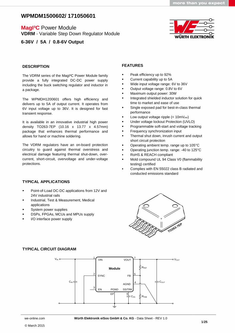
TYPICAL CIRCUIT DIAGRAM
CIN
SYNC
VIN
EN PGND SS/TRK
FB
VOUT
Module RFBT
RFBBCSS
COUT
AGND
1
2
3
EP 6
4
5
7VIN VOUT
TO263-7EP
we-online.com
Würth Elektronik eiSos GmbH & Co. KG - Data Sheet - REV 1.0
2/25
WPMDM1500602/ 171050601
MagI³C Power Module VDRM - Variable Step Down Regulator Module
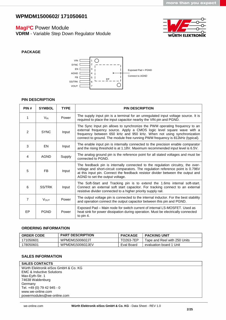
PACKAGE
PIN DESCRIPTION
PIN # SYMBOL TYPE PIN DESCRIPTION
1 VIN Power The supply input pin is a terminal for an unregulated input voltage source. It is required to place the input capacitor nearby the VIN pin and PGND.
2 SYNC Input
The Sync Input pin allows to synchronize the PWM operating frequency to an external frequency source. Apply a CMOS logic level square wave with a frequency between 650 kHz and 950 kHz. When not using synchronization connect to ground. The module free running PWM frequency is 812kHz (typical).
3 EN Input The enable input pin is internally connected to the precision enable comparator and the rising threshold is at 1.18V. Maximum recommended input level is 6.5V.
4 AGND Supply The analog ground pin is the reference point for all stated voltages and must be connected to PGND.
5 FB Input
The feedback pin is internally connected to the regulation circuitry, the over-voltage and short-circuit comparators. The regulation reference point is 0.796V at this input pin. Connect the feedback resistor divider between the output and AGND to set the output voltage.
6 SS/TRK Input The Soft-Start and Tracking pin is to extend the 1.6ms internal soft-start. Connect an external soft start capacitor. For tracking connect to an external resistive divider connected to a higher priority supply rail.
7 VOUT Power The output voltage pin is connected to the internal inductor. For the best stability and operation connect the output capacitor between this pin and PGND.
EP PGND Power Exposed Pad – Main node for switch current of internal LS-MOSFET. Used as heat sink for power dissipation during operation. Must be electrically connected to pin 4.
ORDERING INFORMATION
ORDER CODE PART DESCRIPTION PACKAGE PACKING UNIT
171050601 WPMDM1500602JT TO263-7EP Tape and Reel with 250 Units
178050601 WPMDM1500602JEV Eval Board evaluation board 1 Unit
SALES INFORMATION
SALES CONTACTS
Würth Elektronik eiSos GmbH & Co. KG EMC & Inductive Solutions Max-Eyth-Str. 1 74638 Waldenburg Germany Tel. +49 (0) 79 42 945 - 0 www.we-online.com [email protected]
SYNC
VIN
EN
AGND
SS/TRK
FB
VOUT
1
2
3
4
5
67
6
7
Exposed Pad = PGND
Connect to AGND
EP
we-online.com
Würth Elektronik eiSos GmbH & Co. KG - Data Sheet - REV 1.0
3/25
WPMDM1500602/ 171050601
MagI³C Power Module VDRM - Variable Step Down Regulator Module
ABSOLUTE MAXIMUM RATINGS
Caution: Exceeding the listed absolute maximum ratings may affect the device negatively and may cause permanent damage.
SYMBOL PARAMETER LIMITS UNIT
VIN Input Voltage to PGND -0.3 to 40 V
EN, SYNC Enable, Sync input to AGND -0.3 to 5.5 V
SS/TRK, FB Soft-start/Track, Feedback input to AGND -0.3 to 2.5 V
AGND AGND to PGND -0.3 to 0.3 V
VESD-HBM ESD, human body model (1)
-2000 to 2000 V
TJ Junction temperature 150 °C
TST Storage temperature -65 to 150 °C
TSOLR Peak case/leads temperature during reflow soldering, max. 20sec (2)
Maximum two cycles!
240 ±5°C °C
OPERATING CONDITIONS
Operating conditions are conditions under which operation of the device is intended to be functional. All values are referenced to GND.
SYMBOL PARAMETER MIN (3)
TYP (4)
MAX (3)
UNIT
VIN Input voltage 6 - 36 V
VOUT Regulated output voltage 0.8 6 V
EN, SYNC Enable, Sync input 0 - 5.0 V
TA Ambient temperature range -40 - note (5)
°C
TJ Junction temperature range -40 - 125 °C
THERMAL SPECIFICATIONS
SYMBOL PARAMETER TYP UNIT
θJA Thermal resistance junction to ambient(6)
12 °C/W
θJC Thermal resistance junction to case, no air flow 1.9 °C/W
TSD Thermal shut down, junction temperature, rising 165 °C
TSD-HYST Thermal shut down hysteresis, falling 15 °C
ELECTRICAL SPECIFICATIONS
MIN and MAX limits are valid for the recommended junction temperature range of -40°C to 125°C. Typical values
represent statistically the utmost probability at following conditions: VIN=12V, VOUT=3.3V, TA=25°C, unless otherwise specified.
SYMBOL PARAMETER CONDITIONS MIN (3)
TYP (4)
MAX (3)
UNIT
IOCP Over current protection 5.4 - - A
VEN EN threshold trip point VEN rising 1.10 1.279 1.458 V
IEN-HYS EN input current VEN > 1.279V - -21 - µA
fSW Free-running oscillator
frequency Sync input connected to ground
711 812 914 kHz
fSYNC Synchronization range 650 - 950 kHz
we-online.com
Würth Elektronik eiSos GmbH & Co. KG - Data Sheet - REV 1.0
4/25
WPMDM1500602/ 171050601
MagI³C Power Module VDRM - Variable Step Down Regulator Module
ELECTRICAL SPECIFICATIONS
MIN and MAX limits are valid for the recommended junction temperature range of -40°C to 125°C. Typical values
represent statistically the utmost probability at following conditions: VIN=12V, VOUT=3.3V, TA=25°C, unless otherwise specified.
SYMBOL PARAMETER CONDITIONS MIN (3)
TYP (4)
MAX (3)
UNIT
VIL-SYNC Synchronization logic
zero amplitude Relative to AGND - - 0.4 V
VIH-SYNC Synchronization logic
zero amplitude Relative to AGND 1.5 - - V
SYNCd.c.
Synchronization duty
cycle range 15 50 85 %
Dmax Maximum duty cycle - 83 - %
ISS Soft-start source current VSS = 0V 40 50 60 µA
tss Internal soft-start time - 1.6 - ms
VFB In-regulation feedback voltage
VSS >+ 0.8V IOUT = 5A
0.776 0.796 0.816 V
VFB-OVP Feedback over-voltage protection threshold
- 0.86 - V
IFB Feedback input bias current
- 5 - nA
IQ Non switching input current
VFB= 0.86V - 2.6 - mA
ISD Shut down quiescent current
VEN= 0V - 70 - µA
ΔVOUT Output voltage ripple COUT=220μF 7mΩ ESR + 100µF X7R + 2x 0.047µF
- 9 - mVpp
ΔVOUT/ΔVIN Line regulation VIN = 12V to 36V IOUT=1mA
- ±0.02 - %
ΔVOÙT/ΔIOUT Load regulation VIN = 12V to 36V IOUT = 1mA to 5A
- 1 - mV/A
η Efficiency VIN=12V, VOUT=3.3V IOUT=1A
- 86 - %
η Efficiency VIN=12V, VOUT=3.3V IOUT=5A
- 81.5 - %
η Efficiency VIN=24V, VOUT=3.3V IOUT=2A
- 80 - %
η Efficiency VIN = 24V, VOUT = 3.3V IOUT = 5A
- 76 - %
NOTES
(1) The human body model is a 100pF capacitor discharged through a 1.5 kΩ resistor into each pin. Test
method is per JESD-22-114.
(2) JEDEC J-STD020
(3) Min and Max limits are 100% production tested at 25°C. Limits over the operating temperature range are
guaranteed through correlation using Statistical Quality Control (SQC) methods.
(4) Typical numbers are valid at 25°C ambient temperature and represent statistically the utmost probability
assuming the Gaussian distribution.
(5) Depending on heat sink design, number of PCB layers, copper thickness and air flow.
(6) Measured on a 3.5” x 3.5” four layer board, with 104µm (3 ounce) copper on outer layers and 70µm (2
ounce) copper on inner layers, sixty 10 mil thermal vias, no air flow, and 1W power dissipation
we-online.com
Würth Elektronik eiSos GmbH & Co. KG - Data Sheet - REV 1.0
5/25
WPMDM1500602/ 171050601
MagI³C Power Module VDRM - Variable Step Down Regulator Module
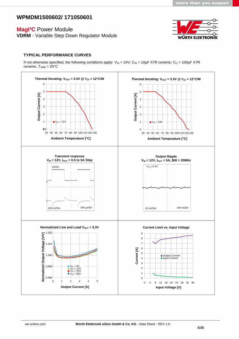
TYPICAL PERFORMANCE CURVES
If not otherwise specified, the following conditions apply: VIN = 24V; CIN = 10µF X7R ceramic; CO = 100µF X7R ceramic, TAMB = 25°C
Ou
tpu
t C
urr
en
t [A
]
Ambient Temperature [°C]
Thermal Derating: VOUT = 3.3V @ θJA = 12°C/W
0.00
1
2
3
4
5
6
30 40 50 60 70 80 90 100 110 120 130
VIN = 12V
Ou
tpu
t C
urr
en
t [A
]Ambient Temperature [°C]
Thermal Derating: VOUT = 3.3V @ θJA = 12°C/W
0
1
2
3
4
5
6
30 40 50 60 70 80 90 100 110 120 130
VIN = 24V
100 mV/Div 500 µs/Div
2A/Div
Transient response
VIN = 12V, IOUT = 0.5 to 5A Step
10 mV/Div 500 ns/Div
VOUT=3.3V
Output Ripple
VIN = 12V, IOUT = 5A, BW = 20MHz
No
rma
lize
d O
utp
ut
Vo
lta
ge
[V
/V]
Output Current [A]
Normalizied Line and Load VOUT = 3.3V
0.998
0.999
1.000
1.001
1.002
0 1 2 3 4 5
VIN = 9VVIN = 12VVIN = 24VVIN = 36V
0
1
2
3
4
5
6
7
8
9
0 4 8 12 16 20 24 28 32 36
Output CurrentInput Current
Cu
rre
nt
[A]
Input Voltage [V]
Current Limit vs. Input Voltage
we-online.com
Würth Elektronik eiSos GmbH & Co. KG - Data Sheet - REV 1.0
6/25
WPMDM1500602/ 171050601
MagI³C Power Module VDRM - Variable Step Down Regulator Module
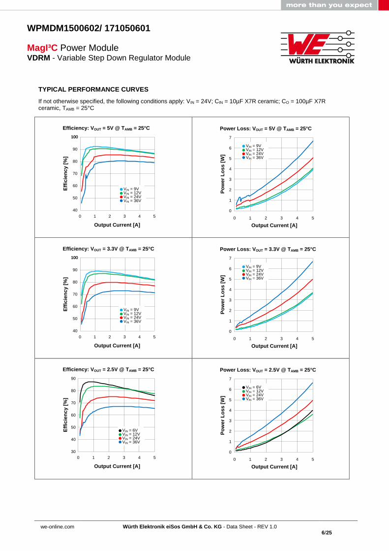
TYPICAL PERFORMANCE CURVES
If not otherwise specified, the following conditions apply: VIN = 24V; CIN = 10µF X7R ceramic; CO = 100µF X7R ceramic, TAMB = 25°C
100
Eff
icie
nc
y [
%]
Output Current [A]
Efficiency: VOUT = 5V @ TAMB = 25°C
VIN = 9VVIN = 12VVIN = 24VVIN = 36V
0 1 2 3 4 5
40
50
60
70
80
90
100
0
1
2
3
4
5
6
7
0 1 2 3 4 5
VIN = 9VVIN = 12VVIN = 24VVIN = 36V
Po
we
r L
os
s [
W]
Output Current [A]
Power Loss: VOUT = 5V @ TAMB = 25°C
100
Eff
icie
nc
y [
%]
Output Current [A]
Efficiency: VOUT = 3.3V @ TAMB = 25°C
VIN = 9VVIN = 12VVIN = 24VVIN = 36V
0 1 2 3 4 5
40
50
60
70
80
90
100
0
1
2
3
4
5
6
7
0 1 2 3 4 5
VIN = 9VVIN = 12VVIN = 24VVIN = 36V
Po
we
r L
os
s [
W]
Output Current [A]
Power Loss: VOUT = 3.3V @ TAMB = 25°C
Eff
icie
nc
y [
%]
Output Current [A]
Efficiency: VOUT = 2.5V @ TAMB = 25°C
0 1 2 3 4 5
30
40
50
60
70
80
90
VIN = 6VVIN = 12VVIN = 24VVIN = 36V
0
1
2
3
4
5
6
7
0 1 2 3 4 5
VIN = 6VVIN = 12VVIN = 24VVIN = 36V
Po
we
r L
os
s [
W]
Output Current [A]
Power Loss: VOUT = 2.5V @ TAMB = 25°C
we-online.com
Würth Elektronik eiSos GmbH & Co. KG - Data Sheet - REV 1.0
7/25
WPMDM1500602/ 171050601
MagI³C Power Module VDRM - Variable Step Down Regulator Module
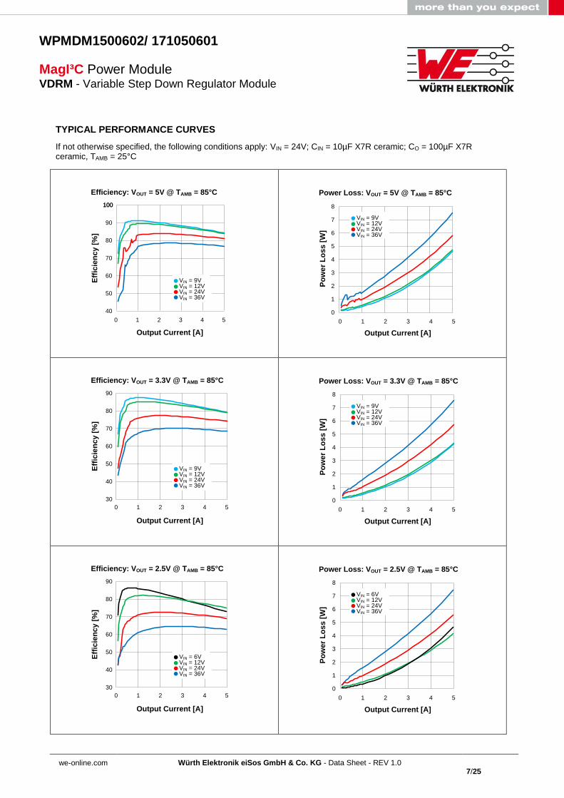
TYPICAL PERFORMANCE CURVES
If not otherwise specified, the following conditions apply: VIN = 24V; CIN = 10µF X7R ceramic; CO = 100µF X7R ceramic, TAMB = 25°C
100
Eff
icie
nc
y [
%]
Output Current [A]
Efficiency: VOUT = 5V @ TAMB = 85°C
VIN = 9VVIN = 12VVIN = 24VVIN = 36V
0 1 2 3 4 5
40
50
60
70
80
90
100
0 1 2 3 4 5
VIN = 9VVIN = 12VVIN = 24VVIN = 36V
Po
we
r L
os
s [
W]
Output Current [A]
Power Loss: VOUT = 5V @ TAMB = 85°C
0
1
2
3
4
5
6
7
8
30
40
50
60
70
80
90
Eff
icie
nc
y [
%]
Output Current [A]
Efficiency: VOUT = 3.3V @ TAMB = 85°C
VIN = 9VVIN = 12VVIN = 24VVIN = 36V
0 1 2 3 4 5
0 1 2 3 4 5
VIN = 9VVIN = 12VVIN = 24VVIN = 36V
Po
we
r L
os
s [
W]
Output Current [A]
Power Loss: VOUT = 3.3V @ TAMB = 85°C
0
1
2
3
4
5
6
7
8
30
40
50
60
70
80
90
Eff
icie
nc
y [
%]
Output Current [A]
Efficiency: VOUT = 2.5V @ TAMB = 85°C
VIN = 6VVIN = 12VVIN = 24VVIN = 36V
0 1 2 3 4 5
0 1 2 3 4 5
VIN = 6VVIN = 12VVIN = 24VVIN = 36V
Po
we
r L
os
s [
W]
Output Current [A]
Power Loss: VOUT = 2.5V @ TAMB = 85°C
0
1
2
3
4
5
6
7
8
we-online.com
Würth Elektronik eiSos GmbH & Co. KG - Data Sheet - REV 1.0
8/25
WPMDM1500602/ 171050601
MagI³C Power Module VDRM - Variable Step Down Regulator Module
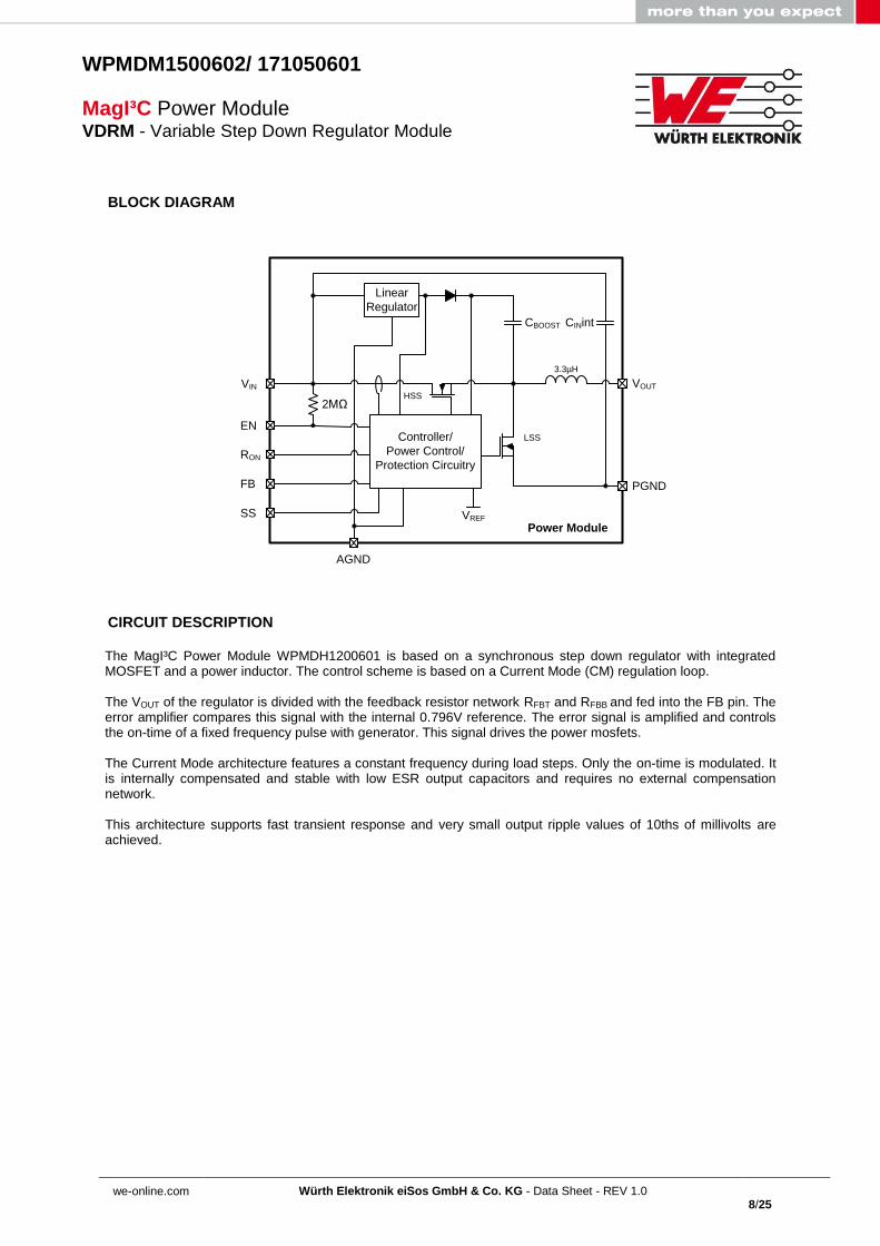
BLOCK DIAGRAM
LSS
HSS
RON
VIN
EN
AGND
SS
FB
VOUT
3.3µH
CBOOST
Power Module
PGND
Controller/
Power Control/
Protection Circuitry
2MΩ
VREF
CINint
Linear
Regulator
CIRCUIT DESCRIPTION
The MagI³C Power Module WPMDH1200601 is based on a synchronous step down regulator with integrated MOSFET and a power inductor. The control scheme is based on a Current Mode (CM) regulation loop. The VOUT of the regulator is divided with the feedback resistor network RFBT and RFBB and fed into the FB pin. The error amplifier compares this signal with the internal 0.796V reference. The error signal is amplified and controls the on-time of a fixed frequency pulse with generator. This signal drives the power mosfets. The Current Mode architecture features a constant frequency during load steps. Only the on-time is modulated. It is internally compensated and stable with low ESR output capacitors and requires no external compensation network. This architecture supports fast transient response and very small output ripple values of 10ths of millivolts are achieved.
we-online.com
Würth Elektronik eiSos GmbH & Co. KG - Data Sheet - REV 1.0
9/25
WPMDM1500602/ 171050601
MagI³C Power Module VDRM - Variable Step Down Regulator Module
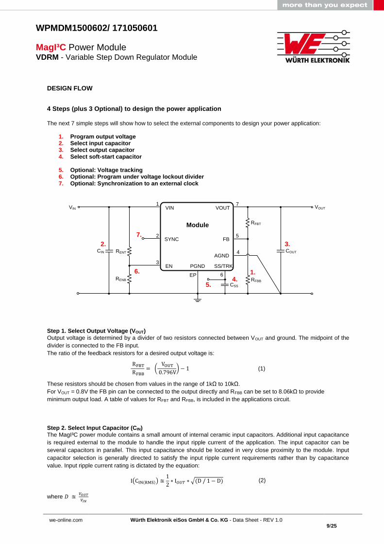
DESIGN FLOW
4 Steps (plus 3 Optional) to design the power application The next 7 simple steps will show how to select the external components to design your power application:
1. Program output voltage 2. Select input capacitor 3. Select output capacitor 4. Select soft-start capacitor
5. Optional: Voltage tracking 6. Optional: Program under voltage lockout divider 7. Optional: Synchronization to an external clock
CIN
SYNC
VIN
EN PGND SS/TRK
FB
VOUT
Module RFBT
RFBB
CSS
COUT
AGND
1
2
3
EP 6
4
5
7
RENT
RENB
1.
7.
2. 3.
4.5.
6.
VIN VOUT
Step 1. Select Output Voltage (VOUT)
Output voltage is determined by a divider of two resistors connected between VOUT and ground. The midpoint of the
divider is connected to the FB input.
The ratio of the feedback resistors for a desired output voltage is:
RFBT
RFBB= (
VOUT
0.796V) − 1 (1)
These resistors should be chosen from values in the range of 1kΩ to 10kΩ.
For VOUT = 0.8V the FB pin can be connected to the output directly and RFBB can be set to 8.06kΩ to provide
minimum output load. A table of values for RFBT and RFBB, is included in the applications circuit.
Step 2. Select Input Capacitor (CIN)
The MagI³C power module contains a small amount of internal ceramic input capacitors. Additional input capacitance
is required external to the module to handle the input ripple current of the application. The input capacitor can be
several capacitors in parallel. This input capacitance should be located in very close proximity to the module. Input
capacitor selection is generally directed to satisfy the input ripple current requirements rather than by capacitance
value. Input ripple current rating is dictated by the equation:
I(CIN(RMS)) ≊1
2∗ I𝑂𝑈𝑇 ∗ √(D / 1 − D) (2)
where 𝐷 ≊ 𝑉𝑂𝑈𝑇
𝑉𝐼𝑁
we-online.com
Würth Elektronik eiSos GmbH & Co. KG - Data Sheet - REV 1.0
10/25
WPMDM1500602/ 171050601
MagI³C Power Module VDRM - Variable Step Down Regulator Module
DESIGN FLOW
(As a point of reference, the worst case ripple current will occur when the module is presented with full load current
and when VIN = 2 * VOUT).
Recommended minimum input capacitance is 22µF X7R (or X5R) ceramic with a voltage rating at least 25% higher
than the maximum applied input voltage for the application. It is also recommended that attention be paid to the
voltage and temperature derating of the capacitor selected. It should be noted that ripple current rating of ceramic
capacitors may be missing from the capacitor data sheet and you may have to contact the capacitor manufacturer for
this parameter.
If the system design requires a certain minimum value of peak-to-peak input ripple voltage (ΔVIN) be maintained then
the following equation may be used.
CIN ≥ 𝐼𝑂𝑈𝑇 ∗ D ∗ (1– D)
fSW−CCM ∗ ΔVIN (3)
If ΔVIN is 1% of VIN for a 12V input to 3.3V output application this equals 120 mV and fSW = 812kHz.
CIN ≥ 5A ∗
3.3V12𝑉
∗ (1–3.3V12𝑉
)
812000 ∗ 0.120V
CIN ≥ 10.2µF
Additional bulk capacitance with higher ESR may be required to damp any resonant effects of the input capacitance
and parasitic inductance of the incoming supply lines. The MagI³C power module typical applications schematic and
evaluation board include a 150μF 50V aluminum capacitor for this function. There are many situations where this
capacitor is not necessary.
Step 3. Select Output Capacitor (COUT)
None of the required COUT output capacitance is contained within the module. A minimum value of 200 μF is required
based on the values of internal compensation in the error amplifier. Low ESR tantalum, organic semiconductor or
specialty polymer capacitor types are recommended for obtaining lowest ripple. The output capacitor COUT may
consist of several capacitors in parallel placed in close proximity to the module. The output capacitor assembly must
also meet the worst case minimum ripple current rating of 0.5 * ILR P-P, as calculated in equation (4) below.
ILR P−P = V𝑂𝑈𝑇 ∗ (V𝐼𝑁 − V𝑂𝑈𝑇)
3.3µH ∗ fSW ∗ V𝐼𝑁 (4)
Beyond that, additional capacitance will reduce output ripple so long as the ESR is low enough to permit it. Loop
response verification is also valuable to confirm closed loop behavior. For applications with dynamic load steps; the
following equation provides a good first pass approximation of COUT for load transient requirements:
COUT ≥ISTEP ∗ VOUT
(VOUT−TRAN − ESR ∙ ISTEP) ∗ fSW (5)
For example:
ISTEP = 4.5𝐴, VOUT = 3.3𝑉, VOUT−TRAN = 100𝑚𝑉
COUT ≥4.5A ∗ 3.3V
(0.1V − 0.007 ∗ 4.5) ∗ 800000
COUT ≥ 271µF
we-online.com
Würth Elektronik eiSos GmbH & Co. KG - Data Sheet - REV 1.0
11/25
WPMDM1500602/ 171050601
MagI³C Power Module VDRM - Variable Step Down Regulator Module
DESIGN FLOW
Note that the stability requirement for 200μF minimum output capacitance will take precedence.
One recommended output capacitor combination is a 220uF, 7 milliohm ESR specialty polymer cap in parallel with a
100µF 6.3V X5R ceramic. This combination provides excellent performance that may exceed the requirements of
certain applications. Additionally some small ceramic capacitors can be used for high frequency EMI suppression.
Step 4. Select Soft-Start Capacitor (CSS)
Programmable soft-start permits the regulator to slowly ramp to its steady state operating point after being enabled,
thereby reducing current inrush from the input supply and slowing the output voltage rise-time to prevent overshoot.
Upon turn-on, after all UVLO conditions have been passed, an internal 1.6ms circuit slowly ramps the SS/TRK input
to implement internal soft start. If 2ms is an adequate turn–on time then the Css capacitor can be left unpopulated.
Longer soft-start periods are achieved by adding an external capacitor to this input.
Soft start duration is given by the formula:
CSS = tSS ∗ 50µA
0.796V (6)
with tss = select soft-start time in (ms)
Using a 0.22μF capacitor results in 3.5ms typical soft-start duration; and 0.47μF results in 7.5ms typical. 0.47μF is a
recommended initial value. As the soft-start input exceeds 0.796V the output of the power stage will be in regulation
and the 50μA current is deactivated. Note that the following conditions will reset the soft-start capacitor by
discharging the SS input to ground with an internal current sink.
The enable input being “pulled low”
Thermal shutdown condition
Internal VCC UVLO (Approx 4.3V input to VIN)
Step 5. Optional: Voltage tracking
The tracking function allows the module to be connected as a slave supply to a primary voltage rail (often the 3.3V
system rail) where the slave module output voltage is lower than that of the master. Proper configuration allows the
slave rail to power up coincident with the master rail such that the voltage difference between the rails during ramp-up
is small (i.e.<0.15V typ). The values for the tracking resistive divider should be selected such that the effect of the
internal 50uA current source is minimized. In most cases the ratio of the tracking divider resistors is the same as the
ratio of the output voltage setting divider. Proper operation in tracking mode dictates the soft-start time of the slave
rail be shorter than the master rail; a condition that is easy satisfy since the CSS cap is replaced by RTKB. The tracking
function is only supported for the power up interval of the master supply; once the SS/TRK rises past 0.8V the input is
no longer enabled and the 50 µA internal current source is switched off.
SS/TRK
INT VCC
50µA
5V VOUT
Rfbt
2.26k
Rfbb
1.07k
FB
3.3V Master
Rtkt
226k
Rtkb
107k
Figure 2. Tracking option input detail
we-online.com
Würth Elektronik eiSos GmbH & Co. KG - Data Sheet - REV 1.0
12/25
WPMDM1500602/ 171050601
MagI³C Power Module VDRM - Variable Step Down Regulator Module
DESIGN FLOW
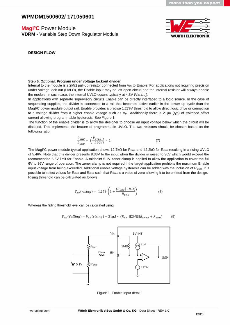
Step 6. Optional: Program under voltage lockout divider
Internal to the module is a 2MΩ pull-up resistor connected from VIN to Enable. For applications not requiring precision
under voltage lock out (UVLO), the Enable input may be left open circuit and the internal resistor will always enable
the module. In such case, the internal UVLO occurs typically at 4.3V (VIN rising).
In applications with separate supervisory circuits Enable can be directly interfaced to a logic source. In the case of
sequencing supplies, the divider is connected to a rail that becomes active earlier in the power-up cycle than the
MagI³C power module output rail. Enable provides a precise 1.279V threshold to allow direct logic drive or connection
to a voltage divider from a higher enable voltage such as VIN. Additionally there is 21μA (typ) of switched offset
current allowing programmable hysteresis. See Figure 1.
The function of the enable divider is to allow the designer to choose an input voltage below which the circuit will be
disabled. This implements the feature of programmable UVLO. The two resistors should be chosen based on the
following ratio:
𝑅𝐸𝑁𝑇
𝑅𝐸𝑁𝐵= (
𝑉𝑈𝑉𝐿𝑂
1.279𝑉) – 1 (7)
The MagI³C power module typical application shows 12.7kΩ for RENB and 42.2kΩ for RENT resulting in a rising UVLO
of 5.46V. Note that this divider presents 8.33V to the input when the divider is raised to 36V which would exceed the
recommended 5.5V limit for Enable. A midpoint 5.1V zener clamp is applied to allow the application to cover the full
6V to 36V range of operation. The zener clamp is not required if the target application prohibits the maximum Enable
input voltage from being exceeded. Additional enable voltage hysteresis can be added with the inclusion of RENH. It is
possible to select values for RENT and RENB such that RENH is a value of zero allowing it to be omitted from the design.
Rising threshold can be calculated as follows:
𝑉𝐸𝑁(𝑟𝑖𝑠𝑖𝑛𝑔) = 1.279 (1 +(𝑅𝐸𝑁𝑇‖2𝑀Ω)
𝑅𝐸𝑁𝐵) (8)
Whereas the falling threshold level can be calculated using:
𝑉𝐸𝑁(𝑓𝑎𝑙𝑙𝑖𝑛𝑔) = 𝑉𝐸𝑁(𝑟𝑖𝑠𝑖𝑛𝑔) − 21µ𝐴 ∗ (𝑅𝐸𝑁𝑇‖2𝑀Ω‖𝑅𝐸𝑁𝑇𝐵 + 𝑅𝐸𝑁𝐻) (9)
RENT
RENH
RENB
VIN
EN
2MΩ
5.1V
RUN
1.279V
5V INT
21µA
Figure 1. Enable input detail
we-online.com
Würth Elektronik eiSos GmbH & Co. KG - Data Sheet - REV 1.0
13/25
WPMDM1500602/ 171050601
MagI³C Power Module VDRM - Variable Step Down Regulator Module
DESIGN FLOW
Step 7. Optional: Synchronization to an external clock
The PWM switching frequency can be synchronized to an external frequency source. If this feature is not used,
connect this input either directly to ground, or connect to ground through a resistor of 1.5kΩ ohm or less. The allowed
synchronization frequency range is 650kHz to 950 kHz. The typical input threshold is 1.4V transition level. Ideally the
input clock should overdrive the threshold by a factor of 2, so direct drive from 3.3V logic via a 1.5kΩ source
resistance is recommended. Note that applying a sustained “logic 1” corresponds to zero hertz PWM frequency and
will cause the module to stop switching.
Determine power losses and thermal requirements of the board
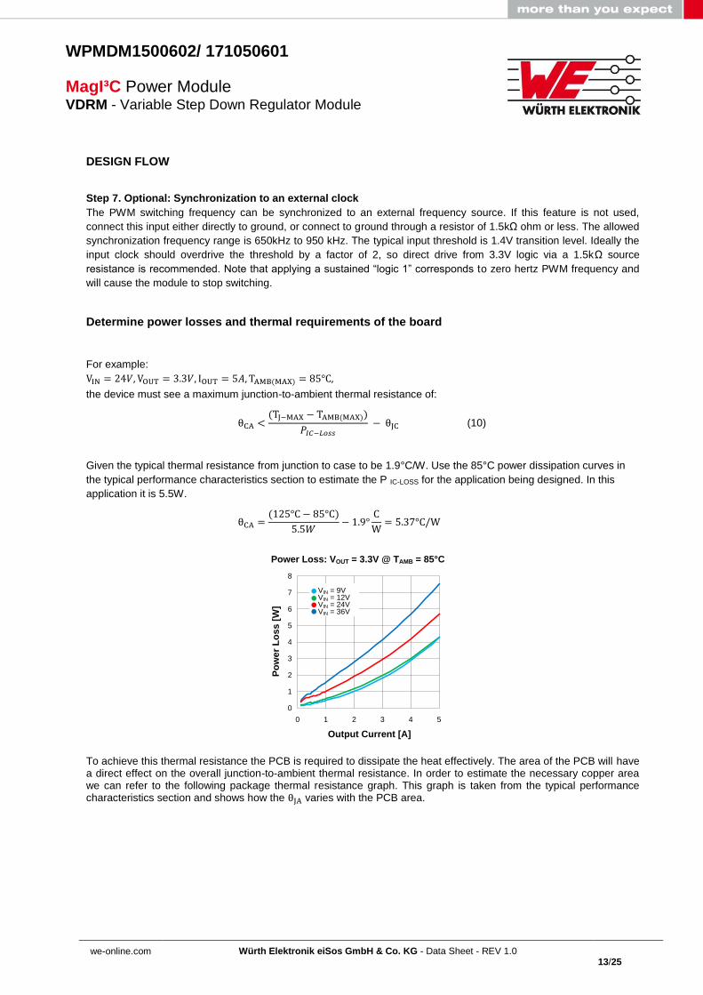
For example:
VIN = 24𝑉, VOUT = 3.3𝑉, IOUT = 5𝐴, TAMB(MAX) = 85°C,
the device must see a maximum junction-to-ambient thermal resistance of:
θCA <(TJ−MAX − TAMB(MAX))
𝑃𝐼𝐶−𝐿𝑜𝑠𝑠 − θJC (10)
Given the typical thermal resistance from junction to case to be 1.9°C/W. Use the 85°C power dissipation curves in
the typical performance characteristics section to estimate the P IC-LOSS for the application being designed. In this
application it is 5.5W.
θCA =(125°C − 85°C)
5.5𝑊− 1.9°
C
W= 5.37°C/W
0 1 2 3 4 5
VIN = 9VVIN = 12VVIN = 24VVIN = 36V
Po
we
r L
os
s [
W]
Output Current [A]
Power Loss: VOUT = 3.3V @ TAMB = 85°C
0
1
2
3
4
5
6
7
8
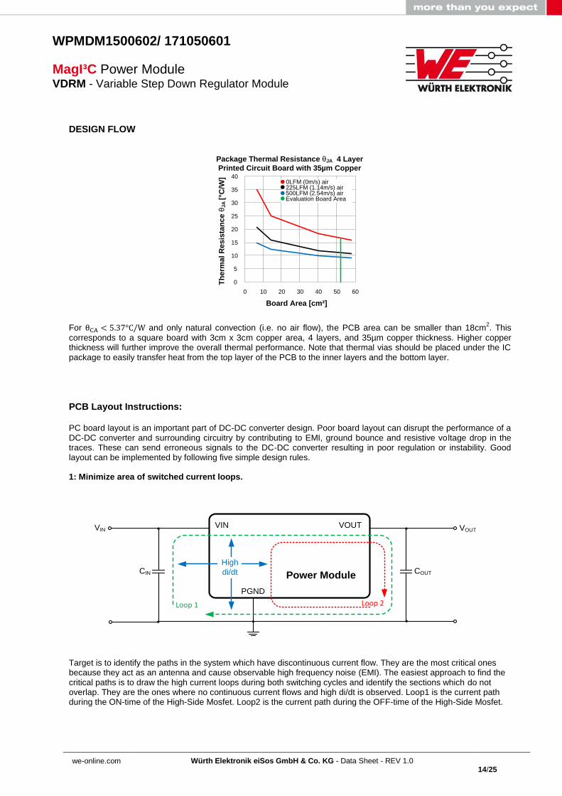
To achieve this thermal resistance the PCB is required to dissipate the heat effectively. The area of the PCB will have a direct effect on the overall junction-to-ambient thermal resistance. In order to estimate the necessary copper area we can refer to the following package thermal resistance graph. This graph is taken from the typical performance characteristics section and shows how the θJA varies with the PCB area.
we-online.com
Würth Elektronik eiSos GmbH & Co. KG - Data Sheet - REV 1.0
14/25
WPMDM1500602/ 171050601
MagI³C Power Module VDRM - Variable Step Down Regulator Module
DESIGN FLOW
Th
erm
al R
es
ista
nc
e θ
JA
[°C
/W]
Board Area [cm²]
Package Thermal Resistance θJA 4 Layer
Printed Circuit Board with 35µm Copper
0LFM (0m/s) air225LFM (1.14m/s) air500LFM (2.54m/s) airEvaluation Board Area
0
5
10
15
20
25
30
35
40
0 10 20 30 40 50 60
For θCA < 5.37°C/W and only natural convection (i.e. no air flow), the PCB area can be smaller than 18cm2. This
corresponds to a square board with 3cm x 3cm copper area, 4 layers, and 35µm copper thickness. Higher copper thickness will further improve the overall thermal performance. Note that thermal vias should be placed under the IC package to easily transfer heat from the top layer of the PCB to the inner layers and the bottom layer.
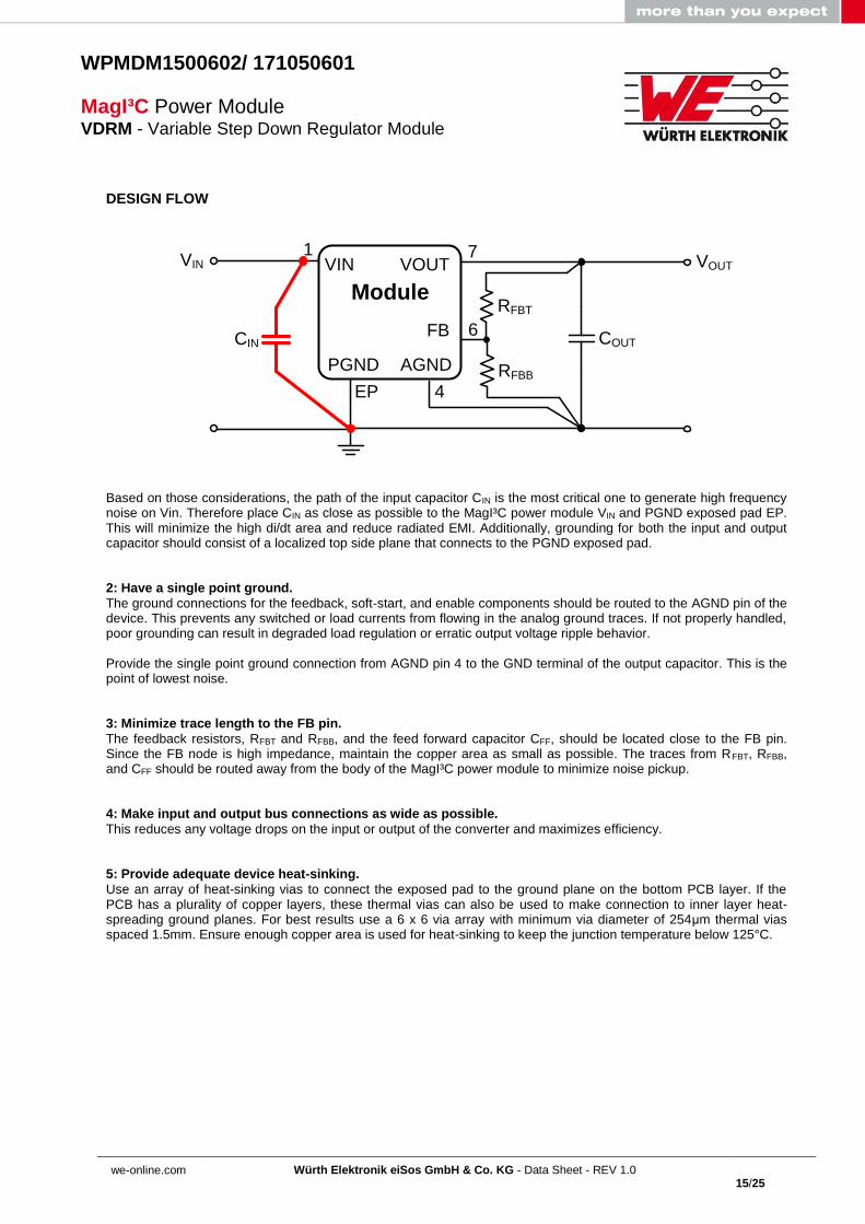
PCB Layout Instructions: PC board layout is an important part of DC-DC converter design. Poor board layout can disrupt the performance of a DC-DC converter and surrounding circuitry by contributing to EMI, ground bounce and resistive voltage drop in the traces. These can send erroneous signals to the DC-DC converter resulting in poor regulation or instability. Good layout can be implemented by following five simple design rules. 1: Minimize area of switched current loops.
CIN
VIN
PGND
VOUT
Power ModuleCOUT
Loop 1 Loop 2
High
di/dt
VIN VOUT
Target is to identify the paths in the system which have discontinuous current flow. They are the most critical ones because they act as an antenna and cause observable high frequency noise (EMI). The easiest approach to find the critical paths is to draw the high current loops during both switching cycles and identify the sections which do not overlap. They are the ones where no continuous current flows and high di/dt is observed. Loop1 is the current path during the ON-time of the High-Side Mosfet. Loop2 is the current path during the OFF-time of the High-Side Mosfet.
we-online.com
Würth Elektronik eiSos GmbH & Co. KG - Data Sheet - REV 1.0
15/25
WPMDM1500602/ 171050601
MagI³C Power Module VDRM - Variable Step Down Regulator Module
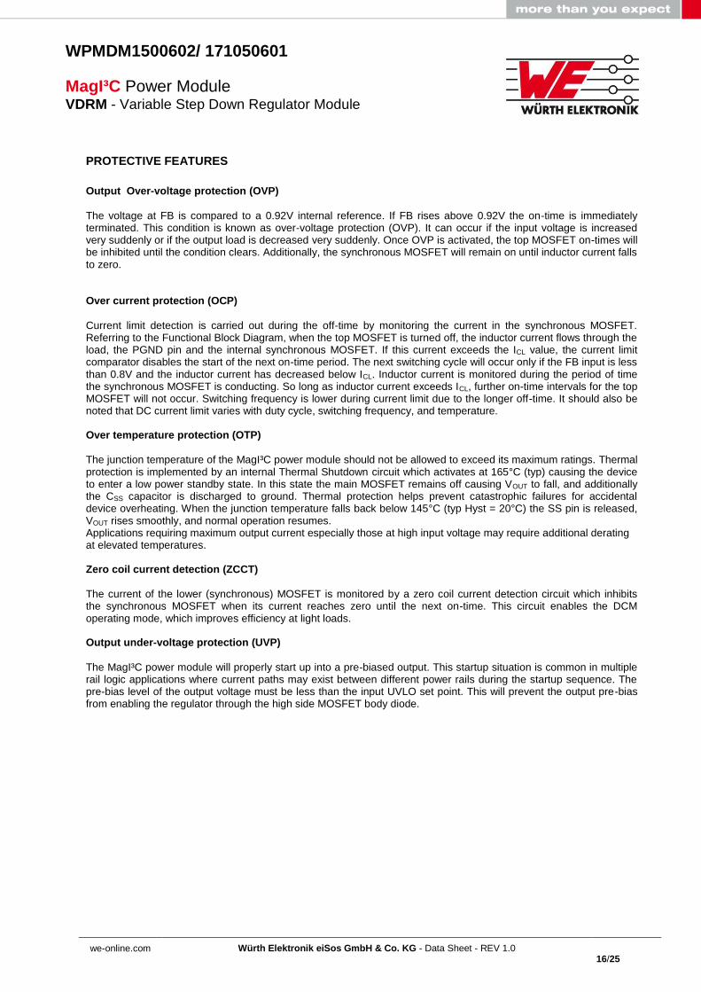
DESIGN FLOW
VIN VIN
FB
PGND
VOUT
ModuleRFBT
RFBB
COUT
AGND
6
7
CIN
1
EP 4
VOUT
Based on those considerations, the path of the input capacitor CIN is the most critical one to generate high frequency noise on Vin. Therefore place CIN as close as possible to the MagI³C power module VIN and PGND exposed pad EP. This will minimize the high di/dt area and reduce radiated EMI. Additionally, grounding for both the input and output capacitor should consist of a localized top side plane that connects to the PGND exposed pad. 2: Have a single point ground.
The ground connections for the feedback, soft-start, and enable components should be routed to the AGND pin of the device. This prevents any switched or load currents from flowing in the analog ground traces. If not properly handled, poor grounding can result in degraded load regulation or erratic output voltage ripple behavior. Provide the single point ground connection from AGND pin 4 to the GND terminal of the output capacitor. This is the point of lowest noise. 3: Minimize trace length to the FB pin.
The feedback resistors, RFBT and RFBB, and the feed forward capacitor CFF, should be located close to the FB pin. Since the FB node is high impedance, maintain the copper area as small as possible. The traces from RFBT, RFBB, and CFF should be routed away from the body of the MagI³C power module to minimize noise pickup. 4: Make input and output bus connections as wide as possible.
This reduces any voltage drops on the input or output of the converter and maximizes efficiency. 5: Provide adequate device heat-sinking.
Use an array of heat-sinking vias to connect the exposed pad to the ground plane on the bottom PCB layer. If the PCB has a plurality of copper layers, these thermal vias can also be used to make connection to inner layer heat-spreading ground planes. For best results use a 6 x 6 via array with minimum via diameter of 254μm thermal vias spaced 1.5mm. Ensure enough copper area is used for heat-sinking to keep the junction temperature below 125°C.
we-online.com
Würth Elektronik eiSos GmbH & Co. KG - Data Sheet - REV 1.0
16/25
WPMDM1500602/ 171050601
MagI³C Power Module VDRM - Variable Step Down Regulator Module
PROTECTIVE FEATURES
Output Over-voltage protection (OVP)
The voltage at FB is compared to a 0.92V internal reference. If FB rises above 0.92V the on-time is immediately terminated. This condition is known as over-voltage protection (OVP). It can occur if the input voltage is increased very suddenly or if the output load is decreased very suddenly. Once OVP is activated, the top MOSFET on-times will be inhibited until the condition clears. Additionally, the synchronous MOSFET will remain on until inductor current falls to zero.
Over current protection (OCP)
Current limit detection is carried out during the off-time by monitoring the current in the synchronous MOSFET. Referring to the Functional Block Diagram, when the top MOSFET is turned off, the inductor current flows through the load, the PGND pin and the internal synchronous MOSFET. If this current exceeds the ICL value, the current limit comparator disables the start of the next on-time period. The next switching cycle will occur only if the FB input is less than 0.8V and the inductor current has decreased below ICL. Inductor current is monitored during the period of time the synchronous MOSFET is conducting. So long as inductor current exceeds ICL, further on-time intervals for the top MOSFET will not occur. Switching frequency is lower during current limit due to the longer off-time. It should also be noted that DC current limit varies with duty cycle, switching frequency, and temperature. Over temperature protection (OTP)
The junction temperature of the MagI³C power module should not be allowed to exceed its maximum ratings. Thermal protection is implemented by an internal Thermal Shutdown circuit which activates at 165°C (typ) causing the device to enter a low power standby state. In this state the main MOSFET remains off causing VOUT to fall, and additionally the CSS capacitor is discharged to ground. Thermal protection helps prevent catastrophic failures for accidental device overheating. When the junction temperature falls back below 145°C (typ Hyst = 20°C) the SS pin is released, VOUT rises smoothly, and normal operation resumes. Applications requiring maximum output current especially those at high input voltage may require additional derating at elevated temperatures. Zero coil current detection (ZCCT)
The current of the lower (synchronous) MOSFET is monitored by a zero coil current detection circuit which inhibits the synchronous MOSFET when its current reaches zero until the next on-time. This circuit enables the DCM operating mode, which improves efficiency at light loads. Output under-voltage protection (UVP)
The MagI³C power module will properly start up into a pre-biased output. This startup situation is common in multiple rail logic applications where current paths may exist between different power rails during the startup sequence. The pre-bias level of the output voltage must be less than the input UVLO set point. This will prevent the output pre-bias from enabling the regulator through the high side MOSFET body diode.
we-online.com
Würth Elektronik eiSos GmbH & Co. KG - Data Sheet - REV 1.0
17/25
WPMDM1500602/ 171050601
MagI³C Power Module VDRM - Variable Step Down Regulator Module
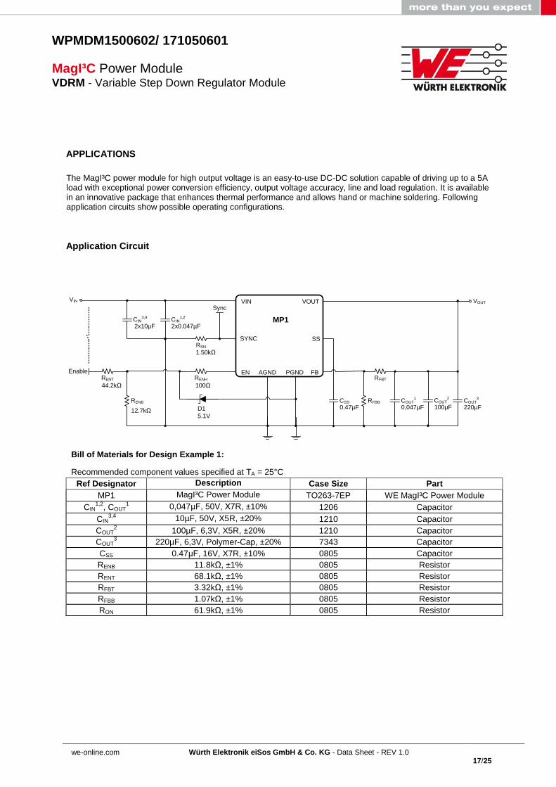
APPLICATIONS
The MagI³C power module for high output voltage is an easy-to-use DC-DC solution capable of driving up to a 5A load with exceptional power conversion efficiency, output voltage accuracy, line and load regulation. It is available in an innovative package that enhances thermal performance and allows hand or machine soldering. Following application circuits show possible operating configurations.
Application Circuit
RSN
SYNC
VIN
EN AGND FB
SS
VOUT
MP1
RENT
RENB RFBBCSS COUT1
Enable
0.47µFCOUT
3
0,047µF 220µF
1.50kΩ
44.2kΩ
12.7kΩ
Sync
RFBT
PGND
CIN1,2
2x0.047µFCIN
3,4
2x10µF
RENH
100Ω
D1
5.1V
COUT2
100µF
VIN VOUT
Bill of Materials for Design Example 1:
Recommended component values specified at TA = 25°C
Ref Designator Description Case Size Part
MP1 MagI³C Power Module TO263-7EP WE MagI³C Power Module
CIN1,2
, COUT1 0,047μF, 50V, X7R, ±10% 1206 Capacitor
CIN3,4
10µF, 50V, X5R, ±20% 1210 Capacitor
COUT2
100µF, 6,3V, X5R, ±20% 1210 Capacitor
COUT3
220µF, 6,3V, Polymer-Cap, ±20% 7343 Capacitor
CSS 0.47μF, 16V, X7R, ±10% 0805 Capacitor
RENB 11.8kΩ, ±1% 0805 Resistor
RENT 68.1kΩ, ±1% 0805 Resistor
RFBT 3.32kΩ, ±1% 0805 Resistor
RFBB 1.07kΩ, ±1% 0805 Resistor
RON 61.9kΩ, ±1% 0805 Resistor
we-online.com
Würth Elektronik eiSos GmbH & Co. KG - Data Sheet - REV 1.0
18/25
WPMDM1500602/ 171050601
MagI³C Power Module VDRM - Variable Step Down Regulator Module
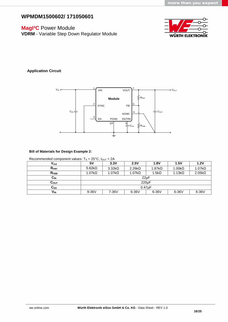
Application Circuit
CIN
SYNC
VIN
EN PGND SS/TRK
FB
VOUT
Module RFBT
RFBBCSS
COUT
AGND
1
2
3
EP 6
4
5
7VIN VOUT
Bill of Materials for Design Example 2:
Recommended component values: TA = 25°C, IOUT = 2A
Vout 5V 3.3V 2.5V 1.8V 1.5V 1.2V
RFBT 5.62kΩ 3.32kΩ 2.26kΩ 1.87kΩ 1.00kΩ 1.07kΩ
RFBB 1.07kΩ 1.07kΩ 1.07kΩ 1.5kΩ 1.13kΩ 2.05kΩ
CIN 22µF
COUT 220µF
CSS 0.47µF
VIN 9-36V 7-36V 6-36V 6-36V 6-36V 6-36V
we-online.com
Würth Elektronik eiSos GmbH & Co. KG - Data Sheet - REV 1.0
19/25
WPMDM1500602/ 171050601
MagI³C Power Module VDRM - Variable Step Down Regulator Module
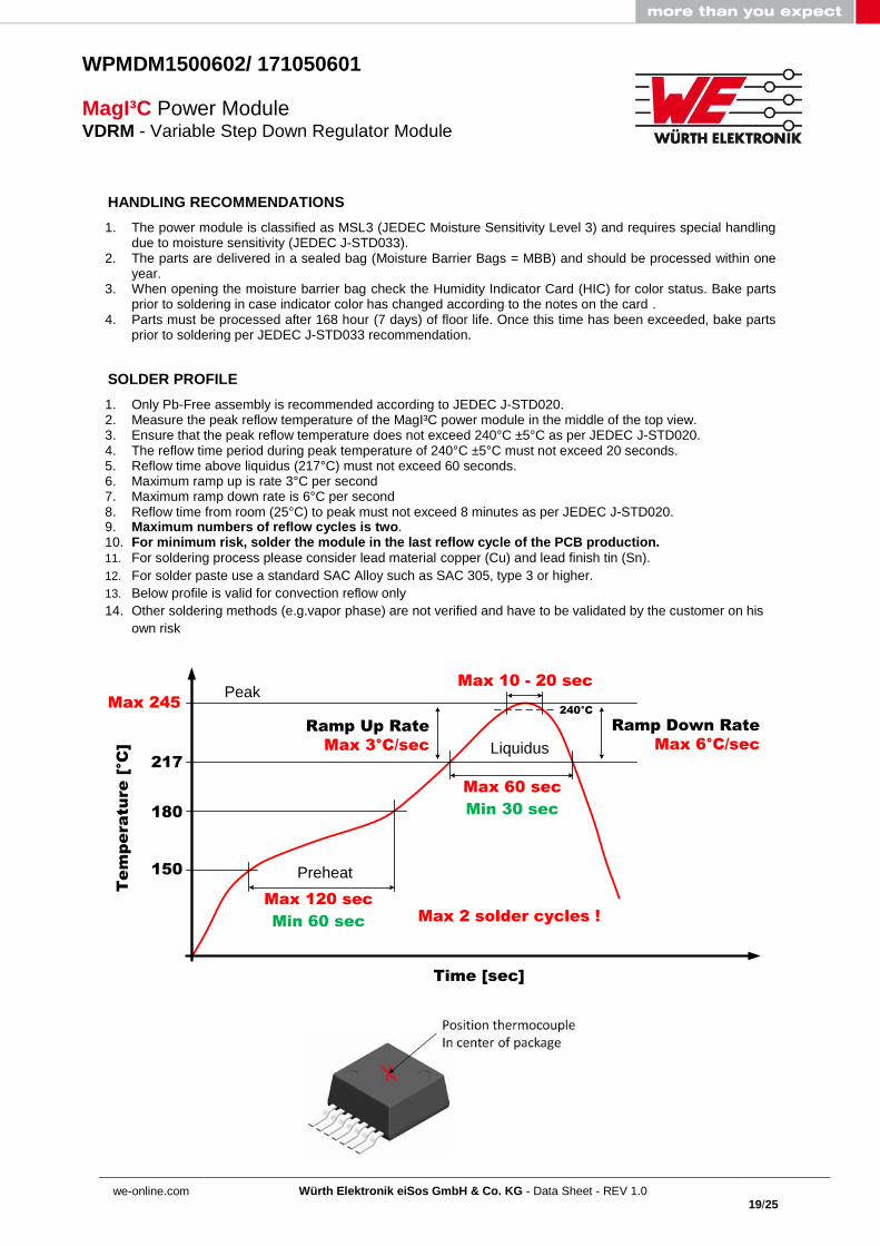
HANDLING RECOMMENDATIONS
1. The power module is classified as MSL3 (JEDEC Moisture Sensitivity Level 3) and requires special handling due to moisture sensitivity (JEDEC J-STD033).
2. The parts are delivered in a sealed bag (Moisture Barrier Bags = MBB) and should be processed within one year.
3. When opening the moisture barrier bag check the Humidity Indicator Card (HIC) for color status. Bake parts prior to soldering in case indicator color has changed according to the notes on the card .
4. Parts must be processed after 168 hour (7 days) of floor life. Once this time has been exceeded, bake parts prior to soldering per JEDEC J-STD033 recommendation.
SOLDER PROFILE
1. Only Pb-Free assembly is recommended according to JEDEC J-STD020. 2. Measure the peak reflow temperature of the MagI³C power module in the middle of the top view. 3. Ensure that the peak reflow temperature does not exceed 240°C ±5°C as per JEDEC J-STD020. 4. The reflow time period during peak temperature of 240°C ±5°C must not exceed 20 seconds. 5. Reflow time above liquidus (217°C) must not exceed 60 seconds. 6. Maximum ramp up is rate 3°C per second 7. Maximum ramp down rate is 6°C per second 8. Reflow time from room (25°C) to peak must not exceed 8 minutes as per JEDEC J-STD020. 9. Maximum numbers of reflow cycles is two. 10. For minimum risk, solder the module in the last reflow cycle of the PCB production.
11. For soldering process please consider lead material copper (Cu) and lead finish tin (Sn).
12. For solder paste use a standard SAC Alloy such as SAC 305, type 3 or higher.
13. Below profile is valid for convection reflow only
14. Other soldering methods (e.g.vapor phase) are not verified and have to be validated by the customer on his
own risk
Te
mp
era
tu
re
[°C
]
Time [sec]
150
180
217
Max 245
Max 120 sec
Min 60 sec
Max 60 sec
Min 30 sec
Max 10 - 20 sec
240°C
Ramp Up Rate
Max 3°C/sec
Ramp Down Rate
Max 6°C/sec
Max 2 solder cycles !
Preheat
Liquidus
Peak
we-online.com
Würth Elektronik eiSos GmbH & Co. KG - Data Sheet - REV 1.0
20/25
WPMDM1500602/ 171050601
MagI³C Power Module VDRM - Variable Step Down Regulator Module
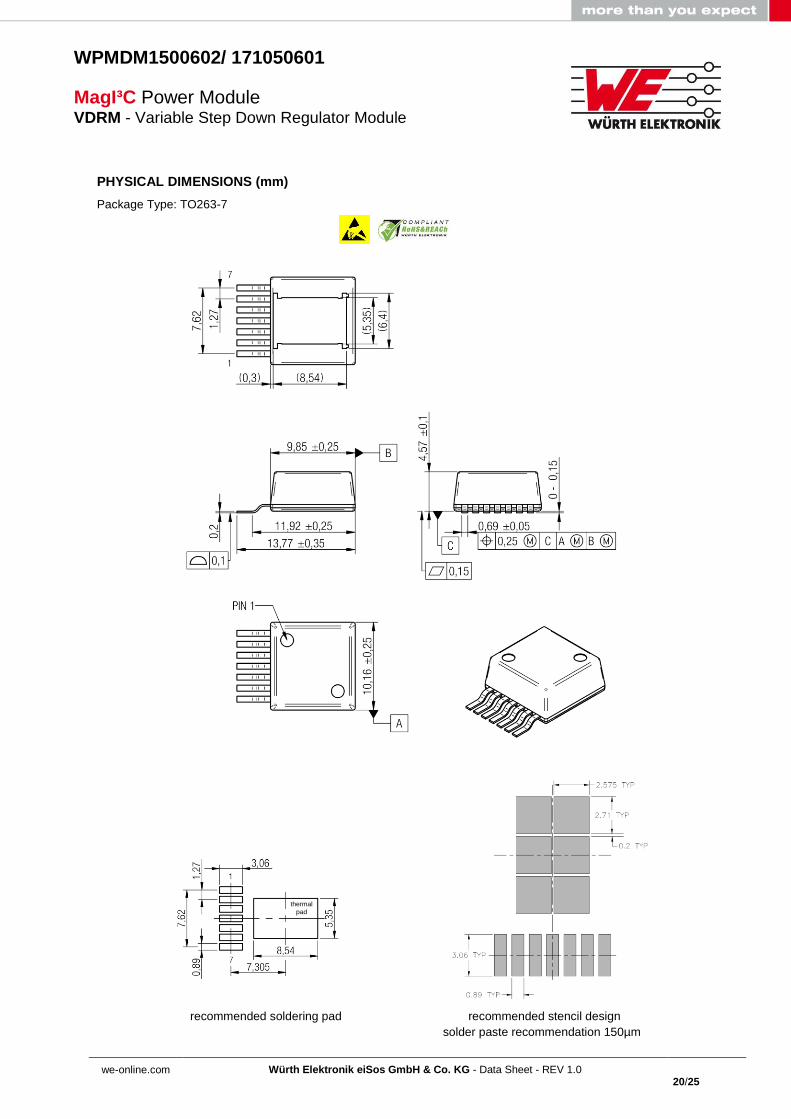
PHYSICAL DIMENSIONS (mm)
Package Type: TO263-7
thermal
pad
recommended soldering pad recommended stencil design
solder paste recommendation 150µm
we-online.com
Würth Elektronik eiSos GmbH & Co. KG - Data Sheet - REV 1.0
21/25
WPMDM1500602/ 171050601
MagI³C Power Module VDRM - Variable Step Down Regulator Module
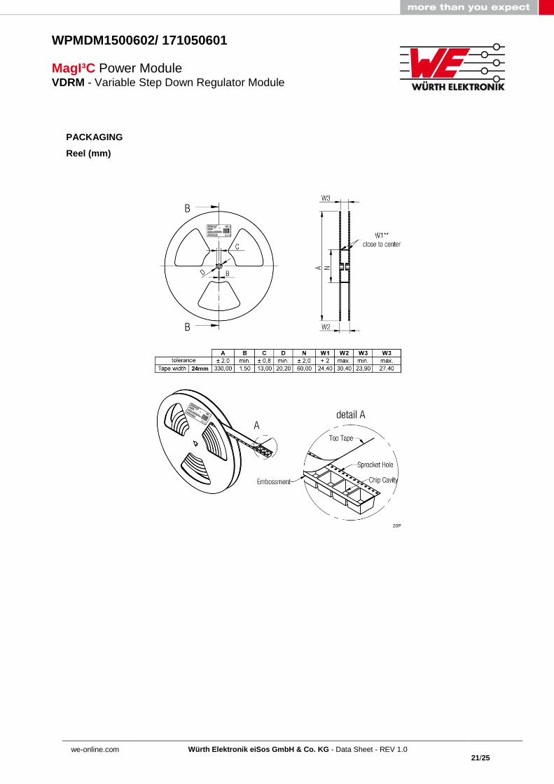
PACKAGING
Reel (mm)
20P
we-online.com
Würth Elektronik eiSos GmbH & Co. KG - Data Sheet - REV 1.0
22/25
WPMDM1500602/ 171050601
MagI³C Power Module VDRM - Variable Step Down Regulator Module
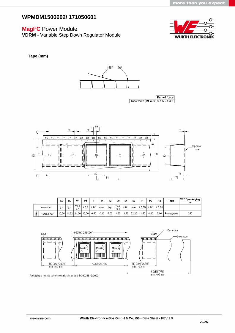
Tape (mm)
TO263-7EP
we-online.com
Würth Elektronik eiSos GmbH & Co. KG - Data Sheet - REV 1.0
23/25
WPMDM1500602/ 171050601
MagI³C Power Module VDRM - Variable Step Down Regulator Module
DOCUMENT HISTORY
Revision Date Description Page
1.0 10.03.2015 Release of final version
we-online.com
Würth Elektronik eiSos GmbH & Co. KG - Data Sheet - REV 1.0
24/25
WPMDM1500602/ 171050601
MagI³C Power Module VDRM - Variable Step Down Regulator Module
CAUTIONS AND WARNINGS
The following conditions apply to all goods within the product series of MagI³C of Würth Elektronik eiSos GmbH & Co. KG: General:
All recommendations according to the general technical specifications of the data-sheet have to be complied with. The usage and operation of the product within ambient conditions which probably alloy or harm the component surface has to be avoided. The responsibility for the applicability of customer specific products and use in a particular customer design is always within the authority of the customer. All technical specifications for standard products do also apply for customer specific products. Residual washing varnish agent that is used during the production to clean the application might change the characteristics of the body, pins or termination. The washing varnish agent could have a negative effect on the long term function of the product. Direct mechanical impact to the product shall be prevented as the material of the body, pins or termination could flake or in the worst case it could break. As these devices are sensitive to electrostatic discharge customer shall follow proper IC Handling Procedures. Customer acknowledges and agrees that it is solely responsible for compliance with all legal, regulatory and safety-related requirements concerning its products, and any use of Würth Elektronik eiSos GmbH & Co. KG components in its applications, notwithstanding any applications-related information or support that may be provided by Würth Elektronik eiSos GmbH & Co. KG. Customer represents and agrees that it has all the necessary expertise to create and implement safeguards which anticipate dangerous consequences of failures, monitor failures and their consequences lessen the likelihood of failures that might cause harm and take appropriate remedial actions. Customer will fully indemnify Würth Elektronik eiSos and its representatives against any damages arising out of the use of any Würth Elektronik eiSos GmbH & Co. KG components in safety-critical applications. Product specific:
Follow all instructions mentioned in the datasheet, especially:
The solder profile has to comply with the technical reflow or wave soldering specification, otherwise this will void the warranty.
All products are supposed to be used before the end of the period of 12 months based on the product date-code.
Violation of the technical product specifications such as exceeding the absolute maximum ratings will void the warranty.
It is also recommended to return the body to the original moisture proof bag and reseal the moisture proof bag again.
ESD prevention methods need to be followed for manual handling and processing by machinery.
we-online.com
Würth Elektronik eiSos GmbH & Co. KG - Data Sheet - REV 1.0
25/25
WPMDM1500602/ 171050601
MagI³C Power Module VDRM - Variable Step Down Regulator Module
IMPORTANT NOTES
The following conditions apply to all goods within the product range of Würth Elektronik eiSos GmbH & Co. KG:
1. General Customer Responsibility
Some goods within the product range of Würth Elektronik eiSos GmbH & Co. KG contain statements regarding general suitability for certain application areas. These statements about suitability are based on our knowledge and experience of typical requirements concerning the areas, serve as general guidance and cannot be estimated as binding statements about the suitability for a customer application. The responsibility for the applicability and use in a particular customer design is always solely within the authority of the customer. Due to this fact it is up to the customer to evaluate, where appropriate to investigate and decide whether the device with the specific product characteristics described in the product specification is valid and suitable for the respective customer application or not. Accordingly, the customer is cautioned to verify that the datasheet is current before placing orders. 2. Customer Responsibility related to Specific, in particular Safety-Relevant Applications
It has to be clearly pointed out that the possibility of a malfunction of electronic components or failure before the end of the usual lifetime cannot be completely eliminated in the current state of the art, even if the products are operated within the range of the specifications. In certain customer applications requiring a very high level of safety and especially in customer applications in which the malfunction or failure of an electronic component could endanger human life or health it must be ensured by most advanced technological aid of suitable design of the customer application that no injury or damage is caused to third parties in the event of malfunction or failure of an electronic component. 3. Best Care and Attention
Any product-specific notes, warnings and cautions must be strictly observed. 4. Customer Support for Product Specifications
Some products within the product range may contain substances which are subject to restrictions in certain jurisdictions in order to serve specific technical requirements. Necessary information is available on request. In this case the field sales engineer or the internal sales person in charge should be contacted who will be happy to support in this matter. 5. Product R&D
Due to constant product improvement product specifications may change from time to time. As a standard reporting procedure of the Product Change Notification (PCN) according to the JEDEC-Standard we inform about minor and major changes. In case of further queries regarding the PCN, the field sales engineer or the internal sales person in charge should be contacted. The basic responsibility of the customer as per Section 1 and 2 remains unaffected. 6. Product Life Cycle
Due to technical progress and economical evaluation we also reserve the right to discontinue production and delivery of products. As a standard reporting procedure of the Product Termination Notification (PTN) according to the JEDEC-Standard we will inform at an early stage about inevitable product discontinuance. According to this we cannot guarantee that all products within our product range will always be available. Therefore it needs to be verified with the field sales engineer or the internal sales person in charge about the current product availability expectancy before or when the product for application design-in disposal is considered. The approach named above does not apply in the case of individual agreements deviating from the foregoing for customer-specific products. 7. Property Rights
All the rights for contractual products produced by Würth Elektronik eiSos GmbH & Co. KG on the basis of ideas, development contracts as well as models or templates that are subject to copyright, patent or commercial protection supplied to the customer will remain with Würth Elektronik eiSos GmbH & Co. KG. Würth Elektronik eiSos GmbH & Co. KG does not warrant or represent that any license, either expressed or implied, is granted under any patent right, copyright, mask work right, or other intellectual property right relating to any combination, application, or process in which Würth Elektronik eiSos GmbH & Co. KG components or services are used. 8. General Terms and Conditions
Unless otherwise agreed in individual contracts, all orders are subject to the current version of the “General Terms and Conditions of Würth Elektronik eiSos Group”, last version available at www.we-online.com.