xc8107 - your analog power ic and the best power
TRANSCRIPT
1/24
XC8107 Series
85mΩ High Function Power Switch
■GENERAL DESCRIPTION The XC8107 series is a P-channel MOSFET power switch IC with a low ON resistance. A current limit, reverse current
prevention (prevents reverse current from VOUT to VIN), soft start, thermal shutdown, and an under voltage lockout (UVLO) are
incorporated as protective functions. A flag function monitors the power switch status.
The flag output has N-channel open drain configuration, and it outputs Low level signal when over-current or overheating is
detected, or when the reverse current prevention is operated. The voltage level which is fed to CE pin determines the status
of XC8107. The logic level of CE pin is selectable between either one of active high or active low.
■APPLICATIONS ●Set Top Boxes
●Digital TVs
●PCs
●USB Ports/USB Hubs
●HDMI
■FEATURES Input Voltage : 2.5V ~ 5.5V
Maximum Output Current : 2A
ON Resistance : 85mΩ@VIN=5.0V (TYP.) *USP-6C
100mΩ@VIN=5.0V (TYP.)*SOT-25 (XC8107A,B)
95mΩ@VIN=5.0V (TYP.) *SOT-25 (XC8107X,Y)
Supply Current : 40μA@ VIN=5.0V
Stand-by Current : 0.1μA (MAX.)
Flag Delay Time : 7.5ms (TYP.)
* At over-current detection
: 4ms (TYP.)
* At reverse voltage detection
Protection Circuit
: Reverse Current Prevention
Thermal Shutdown
Under Voltage Lockout(UVLO)
Soft-start
Functions : Flag Output
CE Pin Input Logic Selectable
Current Limit Response Time : 2μs(TYP.) *Reference value
Operating Ambient Temperature : -40℃ ~ 105℃
Packages : USP-6C
SOT-25 (Au wire or Cu wire)
Environmentally Friendly : EU RoHS Compliant, Pb Free
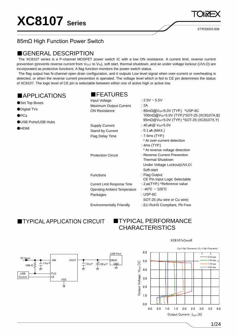
■TYPICAL APPLICATION CIRCUIT
ETR33003-008
■TYPICAL PERFORMANCE CHARACTERISTICS
VOUTVIN
VSS
FLG
CE
USB Port
100kΩ1.0μF
5V Input
USBControl
+120μF1.0μF
VBUS
GND
XC8107xCxxxR
0.0
1.0
2.0
3.0
4.0
5.0
6.0
0.0 0.5 1.0 1.5 2.0 2.5 3.0 3.5 4.0
Output Current : IOUT [A]
Outp
ut
Voltag
e :
VO
UT [V
]
0.5A type
1.0A type
1.5A type
2.0A type
CIN=1.0μ F(ceramic), CL=1.0μ F(ceramic)

2/24
XC8107 Series
■BLOCK DIAGRAM
* Diodes inside the circuit are an ESD protection diode and a parasitic diode.
VIN VOUT
VSS
FLG
CE ON/OFFControl
each circuit
CONTROLUVLO
THERMALSHUTDOWN
CURRENTLIMIT
7.5msDelay
CURRENTSENSE
Reverse Current
Prevention
4msDelay
3/24
XC8107 Series
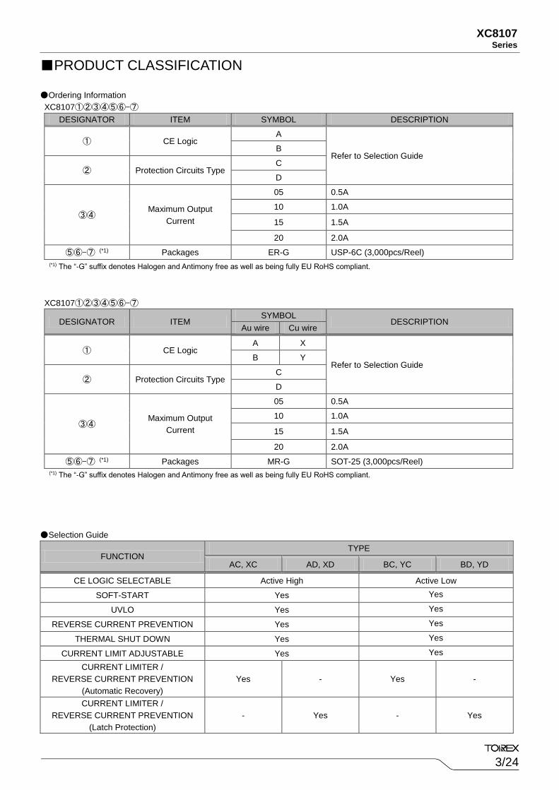
■PRODUCT CLASSIFICATION
●Ordering Information
XC8107①②③④⑤⑥-⑦
DESIGNATOR ITEM SYMBOL DESCRIPTION
① CE Logic A
Refer to Selection Guide B
② Protection Circuits Type C
D
③④ Maximum Output
Current
05 0.5A
10 1.0A
15 1.5A
20 2.0A
⑤⑥-⑦ (*1) Packages ER-G USP-6C (3,000pcs/Reel)
(*1) The “-G” suffix denotes Halogen and Antimony free as well as being fully EU RoHS compliant.
XC8107①②③④⑤⑥-⑦
DESIGNATOR ITEM SYMBOL
DESCRIPTION Au wire Cu wire
① CE Logic A X
Refer to Selection Guide B Y
② Protection Circuits Type C
D
③④ Maximum Output
Current
05 0.5A
10 1.0A
15 1.5A
20 2.0A
⑤⑥-⑦ (*1) Packages MR-G SOT-25 (3,000pcs/Reel)
(*1) The “-G” suffix denotes Halogen and Antimony free as well as being fully EU RoHS compliant.
●Selection Guide
FUNCTION TYPE
AC, XC AD, XD BC, YC BD, YD
CE LOGIC SELECTABLE Active High Active Low
SOFT-START Yes Yes
UVLO Yes Yes
REVERSE CURRENT PREVENTION Yes Yes
THERMAL SHUT DOWN Yes Yes
CURRENT LIMIT ADJUSTABLE Yes Yes
CURRENT LIMITER /
REVERSE CURRENT PREVENTION
(Automatic Recovery)
Yes - Yes -
CURRENT LIMITER /
REVERSE CURRENT PREVENTION
(Latch Protection)
- Yes - Yes

4/24
XC8107 Series
■PIN CONFIGURATION
■PIN ASSIGNMENT
PIN NAME PIN NAME FUNCTIONS
USP-6C SOT-25
1 1 VOUT Output
2 - NC No connection
3 3 FLG Fault Report
4 4 CE ON/OFF Control
5 2 VSS Ground
6 5 VIN Power Input
■FUNCTION
* Avoid leaving the CE pin open; set to any fixed voltage.
PIN NAME TYPE Signal STATUS
CE
A, X
H Active
L Stand-by
OPEN Undefined State (*1)
B, Y
H Stand-by
L Active
OPEN Undefined State (*1)
USP-6C(BOTTOM VIEW)
5
6
4
1
2
3
VSS
VIN
CE
NC
FLG
VOUT
1
3
2
5
4
VOUT VIN
VSS
SOT-25(TOP VIEW)
FLG CE
USP-6C (BOTTOM VIEW)
SOT-25 (TOP VIEW)
* The dissipation pad for the USP-6C packages should be solder-plated for mounting strength and heat dissipation.
Please refer to the reference mount pattern and metal masking. The dissipation pad should be connected to the VSS (No. 5) pin.

5/24
XC8107 Series
■ABSOLUTE MAXIMUM RATINGS
PARAMETER SYMBOL RATINGS UNITS
Input Voltage VIN -0.3 ~ 6.0 V
Output Voltage VOUT -0.3 ~ 6.0 V
CE Input Voltage VCE -0.3 ~ 6.0 V
FLG Pin Voltage VFLG -0.3 ~ 6.0 V
FLG Pin Current IFLG 15 mA
Power Dissipation
(Ta=25℃)
USP-6C
Pd
120
mW
1000 (40mm x 40mm Standard board) (*1)
1250 (JESD51-7 board) (*1)
SOT-25
250
600 (40mm x 40mm Standard board) (*1)
760 (JESD51-7 board) (*1)
Operating Ambient Temperature Topr -40 ~ 105 ℃
Storage Temperature Tstg -55 ~ 125 ℃
* All voltages are described based on the VSS.
(*1) The power dissipation figure shown is PCB mounted and is for reference only.
Please refer to PACKAGING INFORMATION for the mounting condition.

6/24
XC8107 Series
■ELECTRICAL CHARACTERISTICS
PARAMETER SYMBOL CONDITIONS MIN. TYP. MAX. UNITS CIRCUIT
Input Voltage VIN - 2.5 - 5.5 V ①
On Resistance RON
USP-6C VIN=3.3V (*1) - 100 110 mΩ
①
VIN=5.0V (*1) - 85 104 mΩ
SOT-25
(XC8107A,B)
VIN=3.3V (*1) - 115 135 mΩ
VIN=5.0V (*1) - 100 120 mΩ
SOT-25
(XC8107X,Y)
VIN=3.3V (*1) 110 130 mΩ
VIN=5.0V (*1) 95 115 mΩ
Supply Current ISS VOUT=OPEN - 40 75 μA ②
Stand-by Current ISTBY
VIN=5.5V, VOUT=OPEN
VCE=VSS (XC8107A,X series)
VCE=VIN (XC8107B,Y series)
- 0.01 1.0 μA ②
Switch Leakage Current ILEAK
VIN=5.5V, VOUT=0V
VCE=VSS (XC8107A,X series)
VCE=VIN (XC8107B,Y series)
- 0.01 1.0 μA ②
Current Limit ILIMT
VOUT=VIN-0.3V,
XC8107xx05 series 0.81 0.90 0.99 A
①
VOUT=VIN-0.3V,
XC8107xx10 series 1.26 1.40 1.54 A
VOUT=VIN-0.3V,
XC8107xx15 series 1.71 1.90 2.09 A
VOUT=VIN-0.3V,
XC8107xx20 series 2.16 2.40 2.64 A
Short-Circuit Current ISHORT
VOUT=0V,
XC8107xx05 series - 0.45 - A
①
VOUT=0V,
XC8107xx10 series - 0.70 - A
VOUT=0V,
XC8107xx15 series - 0.95 - A
VOUT=0V,
XC8107xx20 series - 1.20 - A
Current Limit Circuit
Response Time (*2) tCLR
VIN=5.0V, VOUT: OPEN→0V
Measure from VOUT=0V
to when current falls below
a certain ILIM value
- 2.0 - μs ①
CE "H" Level Voltage VCEH VIN=5.5V, XC8107A,X series 1.5 - 5.5
V ① VIN=5.5V, XC8107B,Y series VSS - 0.8
CE "L" Level Voltage VCEL VIN=5.5V, XC8107A,X series VSS - 0.8
V ① VIN=5.5V, XC8107B,Y series 1.5 - 5.5
CE "H" Level Current ICEH VIN=5.5V, VCE=5.5V -0.1 - 0.1 μA ①
CE "L" Level Current ICEL VIN=5.5V, VCE=0V -0.1 - 0.1 μA ①
UVLO Detected Voltage VUVLOD VIN: 2.2V→1.7V 1.8 1.9 2.0 V ①
UVLO Released Voltage VUVLOR VIN: 1.7V→2.2V 1.9 2.0 2.1 V ①
UVLO Hysteresis VUHYS - - 0.1 - V ①
NOTE:
Unless otherwise stated, VIN=5.0V, IOUT=1mA, VCE=VIN (XC8107A, X series) or VCE=VSS (XC8107B, Y series)
(*1) IOUT=0.25A (XC8107xx05 series), IOUT=0.5A (XC8107xx10 series), IOUT=0.75A (XC8107xx15series), IOUT=1.0A (XC8107xx20 series)
(*2) Design reference value. This parameter is provided only for reference.
Ta=25℃

7/24
XC8107 Series
■ELECTRICAL CHARACTERISTICS (Continued)
PARAMETER SYMBOL CONDITIONS MIN. TYP. MAX. UNITS CIRCUIT
turn-on time tON RLOAD=10Ω, VCE=0V→2.2V - 0.60 1.00 ms ①
turn-off time tOFF RLOAD=10Ω, VCE=2.2V→0V - 0.08 0.13 ms ①
FLG output FET
On-resistance RFLG IFLG=10mA, VOUT=5.5V - 15 20 Ω ③
FLG output FET
Leakage Current IFOFF VIN=5.5V, VFLG=5.5V, VOUT=OPEN - 0.01 0.1 μA ③
FLG delay time
tFD1 over-current condition 6.5 7.5 8.5 ms ①
tFD2 reverse-voltage condition 2.7 4.0 4.7 ms ①
Reverse Current IREV
N=0V, VOUT=5.5V
VCE=5.0V (XC8107A,X series)
VCE=VSS (XC8107B,Y series)
- 0.1 1.0 μA ①
Reverse Current
Prevention
Detect Voltage
VREV_D VIN: 5.0V→4.7V
VOUT=5.0V
USP-6C - 140 -
mV ① SOT-25
(XC8107A,B) - 170 -
SOT-25
(XC8107X,Y) - 160 -
Thermal Shutdown
Detect Temperature TTSD Junction Temperature - 150 - ℃ ①
Thermal Shutdown
Release Temperature TTSR Junction Temperature - 130 - ℃ ①
Thermal Shutdown
Hysteresis Width THYS Junction Temperature - 20 - ℃ ①
NOTE:
Unless otherwise stated, VIN=5.0V, IOUT=1mA, VCE=VIN (XC8107A, X series) or VCE=VSS (XC8107B, Y series)
■TIMING CHART
●turn-on time, turn-off time
90%
tON
VCE
VOUT 10%
tOFF
CE "H" Level Voltage
Voltege[V]
Time[ms]
CE "L" Level Voltage
90%
tON
VCE
VOUT 10%
tOFF
Voltege[V]
Time[ms]
CE "H" Level Voltage
CE "L" Level Voltage
XC8107 Series, Type A, X XC8107 Series, Type B, Y
Ta=25℃

8/24
XC8107 Series
■TEST CIRCUITS
CIN=1.0μF, CL=1.0μF
IOUT
V
A
V
VIN
CEVSS
VOUT
CIN
(ceramic)
FLG
RFLG=100kΩ
V
A
Measurement Waveform
Measurement Waveform
A
CL
(ceramic)
VIN VOUTVCE
A VIN
CEVSS
VOUT
FLG
RFLG=100kΩ
VIN
1) CIRCUIT①
2) CIRCUIT②
3) CIRCUIT③
VV
VIN
CEVSS
VOUT
CIN
(ceramic)
FLG
V
A
V
VIN VOUTVFLG VCE
CL
(ceramic)
↓
9/24
XC8107 Series
■OPERATIONAL EXPLANATION
The XC8107 series is a P-channel MOSFET power switch IC.
The XC8107 series consists of a CE circuit, UVLO circuit, thermal shutdown circuit, current limiter circuit, reverse current
prevention circuit, control block and others. The gate voltage of the power switch transistor is controlled with control block. The
current limiter circuit and reverse current prevention circuit will operate based on the output voltage and output current.
BLOCK DIAGRAM
<CE Pin>
The voltage level which is fed to CE pin controls the status of this IC. If either “H” level or “L” level which is defined as the electrical
specification is fed to CE pin, then XC8107 can operate in standard manner. However, if the middle voltage which is neither “H”
level nor “L” level is fed to CE pin, the consumption current will increase due to the shoot-through current at internal circuits. Also
if CE pin is open, the status of XC8107 cannot be fixed and the behavior will be unstable.
<Thermal Shutdown>
For protection against heat damage of the ICs, thermal shutdown function is built in. When the internal junction temperature
reaches the temperature limit, the thermal shutdown circuit operates and the power switch transistor will turn OFF. The IC resumes
its operation when the thermal shutdown function is released and the IC’s operation is automatically restored because the junction
temperature drops to the level of the thermal shutdown release temperature. When the thermal shutdown circuit detects higher
junction temperature than the detect temperature, the voltage level of FLG pin is low level. When the thermal shutdown circuit
detects lower junction temperature than the release temperature, the thermal shutdown function is released and the voltage level
of FLG pin is high level.
<Under Voltage Lockout (UVLO) >
When the VIN pin voltage goes down to lower voltage than UVLO detected voltage, the power switch transistor turns OFF by
UVLO function in order to prevent false output caused by unstable operation of the internal circuitry. When the VIN pin voltage
goes up to higher voltage than UVLO released voltage, the UVLO function is released and the power switch transistor can turn
ON.
<Soft-start Function>
The soft-start circuit can reduce the in-rush current charged on the output capacitor when IC starts up. Additionally, due to the
reduction of the in-rush current, the circuit can reduce the fluctuation of the input voltage as well. The soft-start time is optimized
internally and defined as turn-on time. (TYP: 0.6ms)
VIN VOUT
VSS
FLG
CE ON/OFFControl
each circuit
CONTROLUVLO
THERMALSHUTDOWN
CURRENTLIMIT
7.5msDelay
CURRENTSENSE
Reverse Current
Prevention
4msDelay
10/24
XC8107 Series
■OPERATIONAL EXPLANATION (Continued) <Current limiter, short-circuit protection>
When the output current reaches the current limit value, the current limit function is activated.
When the current limiting function operates, the constant current limiting circuit operates to reduce the output voltage while
maintaining the output current.
The short-circuit protection function operates when the output voltage drops below 0.7V (TYP.).
The behavior after the current limit or short circuit protection function is activated differs depending on the product type. The
operation of each type is as follows.
Automatic Recovery type: C type
After 7.5ms (TYP.) has passed since the current limiting function was activated, the FLG pin changes to Low level output.
After the short-circuit protection function operates, the output current is reduced to the short-circuit current.
If the overcurrent state continues, this state is maintained.
When the overcurrent state is resolved and the state below the maximum output current continues for 7.5ms (TYP.), the FLG pin
returns to High level output.
Latch off type: D type
After 7.5ms (TYP.) elapses when the current limiting function is activated, the FLG pin changes to Low level output and the
switch transistor turns off. The off state is maintained regardless of whether the overcurrent state is resolved.
Latch operation is released by turning off the IC with the CE pin signal and then restarting, or by lowering the input voltage
below the UVLO detected voltage once and after that raising it higher than UVLO released voltage.
<Reverse current prevention>
An internal circuit is built in that prevents reverse current from the VOUT pin to the VIN pin.
When the difference between input voltage and VOUT pin voltage is higher than the detect voltage set internally, the reverse current
prevention circuit activates, and the power switch transistor turns off, then the reverse current from the VOUT pin to the VIN pin is
reduced to 0.1μA (TYP.).
If the reverse-voltage state lasts for 4ms (TYP.), the FLG pin changes to Low level output.
The behavior after the reverse current prevention function is activated differs depending on the product type. The operation of
each type is as follows.
Automatic Recovery type: C type
On the auto recovery type, when the output voltage drops below the input voltage, the reverse current prevention circuit stops
immediately, and the power switch transistor turns on again. If the output voltage remains lower than the input voltage for 4ms
(TYP.), the FLG pin returns to High level output.
Latch off type: D type
On the latch off type, the power switch transistor remains in the off state even if the reverse voltage state is released.
Latch operation is released by turning off the IC with the CE pin signal and then restarting, or by lowering the input voltage below
the UVLO detected voltage once and after that raising it higher than UVLO released voltage.

11/24
XC8107 Series
■OPERATIONAL EXPLANATION (Continued)
<Flag function>
The flag circuit is built in which monitors the state of the power switch.
The FLG pin outputs Low level when the reverse current prevention function is operating. A resistance of 10kΩ to 100kΩ is
recommended for the FLG pin pull-up resistance.
The pull-up voltage should be 5.5V or less.
Automatic Recovery type: C type
CONDITION FLG pin
Low level output Condition
FLG pin
High level output Condition
Current limiter 7.5ms(TYP.) after maintaining over-current
detection state 7.5ms(TYP.) after over-current release
Short Protection
Reverse current
prevention
4.0ms(TYP.) after maintaining reverse
voltage detection state 4.0ms(TYP.) after reverse voltage release
Thermal shutdown Same time as overheat state is detected Same time as overheat state is released
UVLO Always High level output
Stand-by
Latch off type: D type
CONDITION FLG pin
Low level output Condition
FLG pin
High level output Condition
Current limiter 7.5ms(TYP.) after maintaining over-current
release state When latch operation is released
Short Protection
Reverse current
prevention
4.0ms(TYP.) after maintaining reverse
voltage release state When latch operation is released
Thermal shutdown Same time as overheat state is detected Same time as overheat state is released
UVLO Always High level output
Stand-by

12/24
XC8107 Series
■NOTES ON USE
1. For the phenomenon of temporal and transitional voltage decrease or voltage increase, the IC may be damaged or deteriorated
if IC is used beyond the absolute MAX. specifications.
2. Where wiring impedance is high, operations may become unstable due to noise depending on output current.
Please keep the resistance low between VIN and VSS wiring in particular.
3. Please place the input capacitor (CIN) and the output capacitor (CL) as close to the IC as possible.
For the input or output capacitor, a capacitance of 1.0μF or higher is recommended.
4. The IC can be broken if the VOUT pin voltage suddenly undershoots to a negative voltage due to an output short circuit between
the VOUT pin and GND, or if the VIN pin voltage overshoots after the current limiting operation and exceeds the rated voltage.
We recommend the following counter measures so that the rated voltage is not exceeded.
(a) To suppress the amount of the undershoot by increasing the output capacitance and slowing down the rate of decreasing
VOUT at the time of short circuit.
(b) To add a SBD between VOUT pin and GND to suppress the undershoot of VOUT pin voltage.
(c) To increase the input capacitor to suppress the overshoot of the VIN pin voltage after the current limiter is activated.
Recommended countermeasure circuit diagram
5. It is recommended to use the output current at 80% or less of the current limit set value (ILIMIT).
6. Torex places an importance on improving our products and its reliability.
However, by any possibility, we would request user fail-safe design and post-aging treatment on system or equipment.
VOUTVIN
VSS
FLG
CE
RFLGCIN
CE
VIN
GND
IC
CL SBD
VOUT
GND
VFLG
FLG
13/24
XC8107 Series
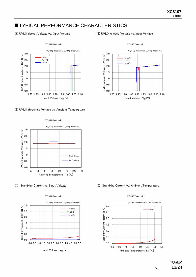
■TYPICAL PERFORMANCE CHARACTERISTICS
(1) UVLO detect Voltage vs. Input Voltage (2) UVLO release Voltage vs. Input Voltage
(3) UVLO threshold Voltage vs. Ambient Temperature
(4) Stand-by Current vs. Input Voltage (5) Stand-by Current vs. Ambient Temperature
0.00
0.01
0.02
0.03
0.04
0.05
0.06
0.07
0.08
0.09
2.0 2.5 3.0 3.5 4.0 4.5 5.0 5.5 6.0
turn
-off t
ime : t
DLY(O
FF) [m
s]
VIN=4.3V, CIN=1.0μ F(ceramic), CL=1.0μ F(ceramic)
4.0
4.5
5.0
5.5
6.0
6.5
7.0
7.5
8.0
8.5
9.0
-50 -25 0 25 50 75 100 125
FLG
ove
r-curr
ent
: t F
D [
ms]
CIN=1.0μ F(ceramic), CL=1.0μ F(ceramic)
XC8107xxxxxR
0.0
0.5
1.0
1.5
2.0
2.5
3.0
1.70 1.75 1.80 1.85 1.90 1.95 2.00 2.05 2.10
Input Voltage : VIN [V]
UV
LO
rele
ase V
oltag
e : U
VLO
[V
]
Ta=105℃
Ta=25℃
Ta=-40℃
CIN=1.0μ F(ceramic), CL=1.0μ F(ceramic)
XC8107xxxxxR
0.0
0.5
1.0
1.5
2.0
2.5
3.0
-50 -25 0 25 50 75 100 125
Ambient Temperature : Ta [℃]
UV
LO
thre
shold
Voltag
e : U
VLO
[V
]
UVLO detect
UVLO release
CIN=1.0μ F(ceramic), CL=1.0μ F(ceramic)
XC8107xxxxxR
0.0
0.5
1.0
1.5
2.0
2.5
3.0
0.0 0.5 1.0 1.5 2.0 2.5 3.0 3.5 4.0 4.5 5.0 5.5
Input Voltage : VIN [V]
Sta
nd-
by C
urr
ent
: Is
tby
[μA
]
Ta=105℃
Ta=25℃
Ta=-40℃
CIN=1.0μ F(ceramic), CL=1.0μ F(ceramic)
XC8107xxxxxR
0.0
0.5
1.0
1.5
2.0
2.5
3.0
1.70 1.75 1.80 1.85 1.90 1.95 2.00 2.05 2.10
Input Voltage : VIN [V]
UV
LO
dete
ct
Voltag
e : U
VLO
[V
]
Ta=105℃
Ta=25℃
Ta=-40℃
CIN=1.0μ F(ceramic), CL=1.0μ F(ceramic)
XC8107xxxxxR
0.0
0.5
1.0
1.5
2.0
2.5
3.0
-50 -25 0 25 50 75 100 125
Ambient Temperature : Ta [℃]
Sta
nd-
by C
urr
ent
: Is
tby
[μA
]
Istby
CIN=1.0μ F(ceramic), CL=1.0μ F(ceramic)
0.0
1.0
2.0
3.0
4.0
5.0
6.0
0.0 0.5 1.0 1.5 2.0 2.5 3.0 3.5 4.0
Outp
ut
Voltag
e : V
OU
T [
V]
CIN=1.0μ F(ceramic), CL=1.0μ F(ceramic)

14/24
XC8107 Series
■TYPICAL PERFORMANCE CHARACTERISTICS (Continued)
(6) Supply Current vs. Input Voltage(sweep up) (7) Supply Current vs. Ambient Temperature
(8) CE "H" Level Voltage vs. Input Voltage (9) CE "L" Level Voltage vs. Input Voltage
(10) CE threshold Voltage vs. Ambient Temperature
-8.0
-6.0
-4.0
-2.0
0.0
2.0
4.0
6.0
8.0
Voltag
e : [
V]
-0.5
0.0
0.5
1.0
1.5
2.0
2.5
3.0
3.5
VCE=0V→5.0V, tr=5μ s, Ta=25℃
VIN=5.0V, CIN=CL=1.0μ F(ceramic)
-8.0
-6.0
-4.0
-2.0
0.0
2.0
4.0
6.0
8.0
Voltag
e : [
V]
-0.5
0.0
0.5
1.0
1.5
2.0
2.5
3.0
3.5
CE Input Voltage
VCE=0V→5.0V, tr=5μ s, IOUT=10Ω , Ta=25℃
VIN=5.0V, CIN=1.0μ F, CL=120μ F(ceramic)
-8.0
-6.0
-4.0
-2.0
0.0
2.0
4.0
6.0
8.0
Voltag
e : [
V]
-0.5
0.0
0.5
1.0
1.5
2.0
2.5
3.0
3.5
VCE=0V→5.0V, tr=5μ s, Ta=25℃
VIN=5.0V, CIN=CL=1.0μ F(ceramic)
XC8107xxxxxR
0
5
10
15
20
25
30
35
40
45
50
0.0 0.5 1.0 1.5 2.0 2.5 3.0 3.5 4.0 4.5 5.0 5.5
Input Voltage : VIN [V]
Supp
ly C
urr
ent
: I S
S [μ
A]
Ta=105℃
Ta=25℃
Ta=-40℃
VIN=5.0V, CIN=1.0μ F(ceramic), CL=1.0μ F(ceramic)
XC8107xxxxxR
0
5
10
15
20
25
30
35
40
45
50
-50 -25 0 25 50 75 100 125
Ambient Temperature : Ta [℃]
Supp
ly C
urr
ent
: I S
S [μ
A]
VIN=5.0V
CIN=1.0μ F(ceramic), CL=1.0μ F(ceramic)
XC8107xxxxxR
0.0
0.5
1.0
1.5
2.0
2.5
3.0
-50 -25 0 25 50 75 100 125
Ambient Temperature : Ta [℃]
CE t
hre
shold
Voltag
e : V
CE [
V]
CE"H"Level
CE"L"Level
CIN=1.0μ F(ceramic), CL=1.0μ F(ceramic)
XC8107xxxxxR
0.0
0.5
1.0
1.5
2.0
2.5
3.0
0.0 0.5 1.0 1.5 2.0 2.5
Input Voltage : VIN [V]
CE "
H" L
eve
l V
oltag
e : V
CEH [
V]
Ta=105℃
Ta=25℃
Ta=-40℃
CIN=1.0μ F(ceramic), CL=1.0μ F(ceramic)
XC8107xxxxxR
0.0
0.5
1.0
1.5
2.0
2.5
3.0
0.0 0.5 1.0 1.5 2.0 2.5
Input Voltage : VIN [V]
CE "
L" L
eve
l V
oltag
e : V
CEL [
V]
Ta=105℃
Ta=25℃
Ta=-40℃
CIN=1.0μ F(ceramic), CL=1.0μ F(ceramic)

15/24
XC8107 Series
■TYPICAL PERFORMANCE CHARACTERISTICS (Continued)
(11) On Resistance vs. Input Voltage (USP-6C) (12) On Resistance
vs. Ambient Temperature (USP-6C)
(13) On Resistance vs. Input Voltage (SOT-25:XC8107A,B) (14) On Resistance
vs. Ambient Temperature (SOT-25:XC8107A,B)
(15) On Resistance vs. Input Voltage (SOT-25:XC8107X,Y) (16) On Resistance
vs. Ambient Temperature (SOT-25:XC8107X,Y)
0
20
40
60
80
100
120
140
160
180
-50 -25 0 25 50 75 100 125
On R
esis
tance :
Ron [m
Ω]
Ambient Temperature : Ta [℃ ]
XC8107xxxxMR
VIN=2.5V
VIN=3.5V
VIN=4.5V
VIN=5.0V
VIN=5.5V
CIN=1.0μF(ceramic), CL=1.0μF(ceramic)
0
20
40
60
80
100
120
140
160
180
2.0 2.5 3.0 3.5 4.0 4.5 5.0 5.5 6.0
On R
esis
tance :
Ron [m
Ω]
Input Voltage : V IN [V]
XC8107xxxxMR
Ta=105℃Ta=25℃Ta=-40℃
CIN=1.0μF(ceramic), CL=1.0μF(ceramic)
0
20
40
60
80
100
120
140
160
180
-50 -25 0 25 50 75 100 125
On R
esis
tance :
Ron [m
Ω]
Ambient Temperature : Ta [℃ ]
XC8107xxxxER
VIN=2.5V
VIN=3.5V
VIN=4.5V
VIN=5.0V
VIN=5.5V
CIN=1.0μF(ceramic), CL=1.0μF(ceramic)
0
20
40
60
80
100
120
140
160
180
2.0 2.5 3.0 3.5 4.0 4.5 5.0 5.5 6.0
On R
esis
tance :
Ron [m
Ω]
Input Voltage : VIN [V]
XC8107xxxxER
Ta=105℃
Ta=25℃
Ta=-40℃
CIN=1.0μF(ceramic), CL=1.0μF(ceramic)
0
20
40
60
80
100
120
140
160
180
-50 -25 0 25 50 75 100 125
On R
esis
tance :
Ron [m
Ω]
Ambient Temperature : Ta [℃ ]
XC8107xxxxMR
VIN=2.5V
VIN=3.5V
VIN=4.5V
VIN=5.0V
VIN=5.5V
CIN=1.0μF(ceramic), CL=1.0μF(ceramic)
0
20
40
60
80
100
120
140
160
180
2.0 2.5 3.0 3.5 4.0 4.5 5.0 5.5 6.0
On R
esis
tance :
Ron [m
Ω]
Input Voltage : V IN [V]
XC8107xxxxMR
Ta=105℃Ta=25℃Ta=-40℃
CIN=1.0μF(ceramic), CL=1.0μF(ceramic)
16/24
XC8107 Series
■TYPICAL PERFORMANCE CHARACTERISTICS (Continued)
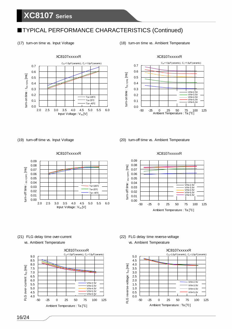
(17) turn-on time vs. Input Voltage (18) turn-on time vs. Ambient Temperature
(19) turn-off time vs. Input Voltage (20) turn-off time vs. Ambient Temperature
(21) FLG delay time over-current (22) FLG delay time reverse-voltage
vs. Ambient Temperature vs. Ambient Temperature
0.0
0.1
0.2
0.3
0.4
0.5
0.6
0.7
-50 -25 0 25 50 75 100 125
turn
-on ti
me :
tD
LY
(ON
)[m
s]
Ambient Temperature : Ta [℃ ]
XC8107xxxxxR
VIN=2.5VVIN=3.5VVIN=4.5VVIN=5.0VVIN=5.5V
CIN=1.0μF(ceramic), CL=1.0μF(ceramic)
0.00
0.01
0.02
0.03
0.04
0.05
0.06
0.07
0.08
0.09
-50 -25 0 25 50 75 100 125
turn
-off
tim
e :
tDL
Y(O
FF
) [m
s]
Ambient Temperature : Ta [℃ ]
XC8107xxxxxR
VIN=2.5VVIN=3.5VVIN=4.5VVIN=5.0VVIN=5.5V
0.00
0.01
0.02
0.03
0.04
0.05
0.06
0.07
0.08
0.09
2.0 2.5 3.0 3.5 4.0 4.5 5.0 5.5 6.0
turn
-off
tim
e :
tDL
Y(O
FF
) [m
s]
Input Voltage : V IN [V]
XC8107xxxxxR
Ta=105℃
Ta=25℃
Ta=-40℃
0.0
0.1
0.2
0.3
0.4
0.5
0.6
0.7
2.0 2.5 3.0 3.5 4.0 4.5 5.0 5.5 6.0
turn
-on ti
me :
tD
LY
(ON
) [m
s]
Input Voltage : V IN [V]
XC8107xxxxxR
Ta=105℃
Ta=25℃
Ta=-40℃
CIN=1.0μF(ceramic), CL=1.0μF(ceramic)
4.0
4.5
5.0
5.5
6.0
6.5
7.0
7.5
8.0
8.5
9.0
-50 -25 0 25 50 75 100 125FLG
over-
curr
ent :
t FD
[ms]
Ambient Temperature : Ta [℃ ]
XC8107xxxxxR
VIN=2.5V
VIN=3.5V
VIN=4.5V
VIN=5.0V
VIN=5.5V
CIN=1.0μF(ceramic), CL=1.0μF(ceramic)
0.0
0.5
1.0
1.5
2.0
2.5
3.0
3.5
4.0
4.5
5.0
-50 -25 0 25 50 75 100 125
FLG
revers
e-v
olta
ge :
t FD
[ms]
Ambient Temperature : Ta [℃ ]
XC8107xxxxxR
VIN=2.5V
VIN=3.5V
VIN=4.5V
VIN=5.0V
CIN=1.0μF(ceramic), CL=1.0μF(ceramic)

17/24
XC8107 Series
■TYPICAL PERFORMANCE CHARACTERISTICS (Continued)
(23) Output Voltage vs. Output Current
(24) turn-on Delay vs. Rise Time (CL=1.0μF) (25) turn-off Delay vs. Fall Time (CL=1.0μF)
(26) turn-on Delay vs. Rise Time (CL=120μF) (27) turn-off Delay vs. Fall Time (CL=120μF)
-0.5
0.0
0.5
1.0
1.5
2.0
2.5
3.0
3.5
-8.0
-6.0
-4.0
-2.0
0.0
2.0
4.0
6.0
8.0
Supply
Curr
ent :
I su
pp
ly[A
]
Volta
ge :
[V]
Time [500μs/div]
XC8107xx10xR
CE Input Voltage
VCE=0V→5.0V, tr=5μs, RL=10Ω, Ta=25℃
VIN=5.0V, CIN=1.0μF, CL=120μF(ceramic)
Output Voltage
Supply Current
-0.5
0.0
0.5
1.0
1.5
2.0
2.5
3.0
3.5
-8.0
-6.0
-4.0
-2.0
0.0
2.0
4.0
6.0
8.0
Supply
Curr
ent :
I su
pp
ly[A
]
Volta
ge :
[V]
Time [500μs/div]
XC8107xx10xR
CE Input Voltage
VCE=5.0V→0V, tf=5μs, RL=10Ω, Ta=25℃VIN=5.0V, CIN=1.0μF, CL=120μF(ceramic)
Output Voltage
Supply Current
-0.5
0.0
0.5
1.0
1.5
2.0
2.5
3.0
3.5
-8.0
-6.0
-4.0
-2.0
0.0
2.0
4.0
6.0
8.0
Supply
Curr
ent :
I su
pp
ly [A
]
Volta
ge :
[V]
Time [100μs/div]
XC8107xx10xR
CE Input Voltage
VCE=5.0V→0V, tf=5μs, RL=10Ω, Ta=25℃
VIN=5.0V, CIN=CL=1.0μF(ceramic)
Output Voltage
Supply Current
-0.5
0.0
0.5
1.0
1.5
2.0
2.5
3.0
3.5
-8.0
-6.0
-4.0
-2.0
0.0
2.0
4.0
6.0
8.0
Supply
Curr
ent :
I su
pp
ly[A
]
Volta
ge :
[V]
Time [100μs/div]
XC8107xx10xR
CE Input Voltage
VCE=0V→5.0V, tr=5μs, RL=10Ω, Ta=25℃
VIN=5.0V, CIN=CL=1.0μF(ceramic)
Output Voltage
Supply Current
0.0
1.0
2.0
3.0
4.0
5.0
6.0
0.0 0.5 1.0 1.5 2.0 2.5 3.0 3.5 4.0
Outp
ut V
olta
ge :
VO
UT
[V]
Output Current : IOUT [A]
XC8107xCxxxR
0.5A type
1.0A type
1.5A type
2.0A type
CIN=1.0μF(ceramic), CL=1.0μF(ceramic)
0.0
1.0
2.0
3.0
4.0
5.0
6.0
0.0 0.5 1.0 1.5 2.0 2.5 3.0 3.5 4.0
Outp
ut V
olta
ge :
VO
UT
[V]
Output Current : IOUT [A]
XC8107xDxxxR
0.5A type
1.0A type
1.5A type
2.0A type
CIN=1.0μF(ceramic), CL=1.0μF(ceramic)
If the over-current state lasts for 7.5ms,the latch off type turns off the power switch transistor.
18/24
XC8107 Series
■TYPICAL PERFORMANCE CHARACTERISTICS (Continued)
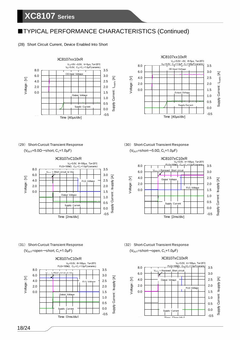
(28) Short Circuit Current, Device Enabled Into Short
(29) Short-Curcuit Transient Response (30) Short-Curcuit Transient Response
(VOUT=5.0Ω→short, CL=1.0μF) (VOUT=short→5.0Ω, CL=1.0μF)
(31) Short-Curcuit Transient Response (32) Short-Curcuit Transient Response
(VOUT=open→short, CL=1.0μF) (VOUT=short→open, CL=1.0μF)
-0.5
0.0
0.5
1.0
1.5
2.0
2.5
3.0
3.5
-8.0
-6.0
-4.0
-2.0
0.0
2.0
4.0
6.0
8.0
Supply
Curr
ent :
I su
pp
ly[A
]
Volta
ge :
[V]
Time [40μs/div]
XC8107xx10xR
CE Input Voltage
VCE=0V→5.0V, tr=5μs, Ta=25℃
VIN=5.0V, CIN=CL=1.0μF(ceramic)
Output Voltage
Supply Current
-0.5
0.0
0.5
1.0
1.5
2.0
2.5
3.0
3.5
-8.0
-6.0
-4.0
-2.0
0.0
2.0
4.0
6.0
8.0
Supply
Curr
ent :
I su
pp
ly[A
]
Volta
ge :
[V]
Time [40μs/div]
XC8107xx10xR
CE Input Voltage
VCE=5.0V→0V, tf=5μs, Ta=25℃
VIN=5.0V, CIN=1.0μF, CL=120μF(ceramic)
Output Voltage
Supply Current
-0.5
0.0
0.5
1.0
1.5
2.0
2.5
3.0
3.5
-8.0
-6.0
-4.0
-2.0
0.0
2.0
4.0
6.0
8.0
Supply
Curr
ent :
Isupply
[A
]
Volta
ge :
[V]
Time [2ms/div]
XC8107xC10xR
FLG Voltage
VIN=5.0V, tf=100μs, Ta=25℃
FLG=100kΩ, CIN=CL=1.0μF(ceramic)
Output Voltage
Supply Current
VOUT = Short circuit to Vss
-0.5
0.0
0.5
1.0
1.5
2.0
2.5
3.0
3.5
-8.0
-6.0
-4.0
-2.0
0.0
2.0
4.0
6.0
8.0
Supply
Curr
ent :
Isupply
[A
]
Volta
ge :
[V]
Time [2ms/div]
XC8107xC10xR
FLG Voltage
VIN=5.0V, tf=100μs, Ta=25℃
FLG=100kΩ, CIN=CL=1.0μF(ceramic)
Output Voltage
Supply Current
VOUT = Short circuit to Vss
-0.5
0.0
0.5
1.0
1.5
2.0
2.5
3.0
3.5
-8.0
-6.0
-4.0
-2.0
0.0
2.0
4.0
6.0
8.0
Supply
Curr
ent :
Isupply
[A
]
Volta
ge :
[V]
Time [2ms/div]
XC8107xC10xR
FLG Voltage
Output Voltage
Supply Current
VIN=5.0V, tr=100μs, Ta=25℃
FLG=100kΩ, CIN=CL=1.0μF(ceramic)
VOUT = Removed Short circuit
-0.5
0.0
0.5
1.0
1.5
2.0
2.5
3.0
3.5
-8.0
-6.0
-4.0
-2.0
0.0
2.0
4.0
6.0
8.0
Supply
Curr
ent :
Isupply
[A
]
Volta
ge :
[V]
Time [2ms/div]
XC8107xC10xR
FLG Voltage
VIN=5.0V, tr=100μs, Ta=25℃FLG=100kΩ, CIN=CL=1.0μF(ceramic)
Output Voltage
Supply Current
VOUT = Removed Short circuit

19/24
XC8107 Series
■TYPICAL PERFORMANCE CHARACTERISTICS (Continued)
(33) Short-Curcuit Transient Response (34) Short-Curcuit Transient Response
(VOUT=5.0Ω→short, CL=120μF) (VOUT=short→5.0Ω, CL=120μF)
(35) Short-Curcuit Transient Response (36) Short-Curcuit Transient Response
(VOUT=open→short, CL=120μF) (VOUT=short→open, CL=120μF)
(37) UVLO Transient Response (CL=1.0μF)
-0.5
0.0
0.5
1.0
1.5
2.0
2.5
3.0
3.5
-8.0
-6.0
-4.0
-2.0
0.0
2.0
4.0
6.0
8.0
Supply
Curr
ent :
I su
pp
ly[A
]
Volta
ge :
[V]
Time [500μs/div]
XC8107xxxxxR
Input Voltage
VIN=0V→5.0V, tr=3ms, Ta=25℃
RL=5Ω, CIN=CL=1.0μF(ceramic)
Output Voltage
Supply Current
-0.5
0.0
0.5
1.0
1.5
2.0
2.5
3.0
3.5
-8.0
-6.0
-4.0
-2.0
0.0
2.0
4.0
6.0
8.0
Supply
Curr
ent :
Is
up
ply
[A
]
Volta
ge :
[V]
Time [500μs/div]
XC8107xxxxxR
Input Voltage
VIN=5.0V→0V, tf=3ms, Ta=25℃
RL=5Ω, CIN=CL=1.0μF(ceramic)
Output Voltage
Supply Current
-0.5
0.0
0.5
1.0
1.5
2.0
2.5
3.0
3.5
-8.0
-6.0
-4.0
-2.0
0.0
2.0
4.0
6.0
8.0
Supply
Curr
ent :
I su
pp
ly[A
]
Volta
ge :
[V]
Time [2ms/div]
XC8107xC10xR
FLG Voltage
VIN=5.0V, tf=100μs, Ta=25℃FLG=100kΩ, CIN=1.0μF, CL=120μF(ceramic)
Output Voltage
Supply Current
VOUT = Short circuit to Vss
-0.5
0.0
0.5
1.0
1.5
2.0
2.5
3.0
3.5
-8.0
-6.0
-4.0
-2.0
0.0
2.0
4.0
6.0
8.0
Supply
Curr
ent :
I su
pp
ly[A
]
Volta
ge :
[V]
Time [2ms/div]
XC8107xC10xR
FLG Voltage
VIN=5.0V, tf=100μs, Ta=25℃FLG=100kΩ, CIN=1.0μF, CL=120μF(ceramic)
Output Voltage
Supply Current
VOUT = Short circuit to Vss
-0.5
0.0
0.5
1.0
1.5
2.0
2.5
3.0
3.5
-8.0
-6.0
-4.0
-2.0
0.0
2.0
4.0
6.0
8.0
Supply
Curr
ent :
I su
pp
ly[A
]
Volta
ge :
[V]
Time [2ms/div]
XC8107xC10xR
FLG Voltage
VIN=5.0V, tr=100μs, Ta=25℃
FLG=100kΩ, CIN=1.0μF, CL=120μF(ceramic)
Output Voltage
Supply Current
VOUT = Removed Short circuit
-0.5
0.0
0.5
1.0
1.5
2.0
2.5
3.0
3.5
-8.0
-6.0
-4.0
-2.0
0.0
2.0
4.0
6.0
8.0
Supply
Curr
ent :
I su
pp
ly[A
]
Volta
ge :
[V]
Time [2ms/div]
XC8107xC10xR
FLG Voltage
VIN=5.0V, tr=100μs, Ta=25℃
FLG=100kΩ, CIN=1.0μF, CL=120μF(ceramic)
Output Voltage
Supply Current
VOUT = Removed Short circuit

20/24
XC8107 Series
■TYPICAL PERFORMANCE CHARACTERISTICS (Continued)
(38) UVLO Transient Response (CL=120μF)
(39) Reverse Voltage Detected Voltage (CL=1.0μF) (40) Reverse Voltage Released Voltage (CL=1.0μF)
(41) Reverse Voltage Detected Voltage (CL=120μF) (42) Reverse Voltage Released Voltage (CL=120μF)
-0.5
0.0
0.5
1.0
1.5
2.0
2.5
3.0
3.5
-8.0
-6.0
-4.0
-2.0
0.0
2.0
4.0
6.0
8.0
Supply
Curr
ent :
I su
pp
ly[A
]
Volta
ge :
[V]
Time [500μs/div]
XC8107xxxxxR
Input Voltage
VIN=0V→5.0V, tr=3ms, Ta=25℃
RL=5Ω, CIN=1.0μF, CL=120μF(ceramic)
Output Voltage
Supply Current
-0.5
0.0
0.5
1.0
1.5
2.0
2.5
3.0
3.5
-8.0
-6.0
-4.0
-2.0
0.0
2.0
4.0
6.0
8.0
Supply
Curr
ent :
I su
pp
ly[A
]
Volta
ge :
[V]
Time [500μs/div]
XC8107xxxxxR
Input Voltage
VIN=5.0V→0V, tf=3ms, Ta=25℃RL=5Ω, CIN=1.0μF, CL=120μF(ceramic)
Output Voltage
Supply Current
-2.0
-1.0
0.0
1.0
2.0
3.0
4.0
5.0
6.0
-8.0
-6.0
-4.0
-2.0
0.0
2.0
4.0
6.0
8.0
Supply
Curr
ent :
Is
up
ply
[A]
Volta
ge :
[V]
Time [500μs/div]
XC8107xxxxxR
Input Voltage
VIN=5.0V, RL=5Ω, Ta=25℃
CIN=CL=1.0μF(ceramic)
Output Voltage
Supply Current
FLG Voltage
VOUT=5.5V forced
-2.0
-1.0
0.0
1.0
2.0
3.0
4.0
5.0
6.0
-8.0
-6.0
-4.0
-2.0
0.0
2.0
4.0
6.0
8.0
Supply
Curr
ent :
I su
pp
ly[A
]
Volta
ge :
[V]
Time [500μs/div]
XC8107xxxxxR
Input Voltage
VIN=5.0V, RL=5Ω, Ta=25℃
CIN=CL=1.0μF(ceramic)
Output Voltage
Supply Current
FLG Voltage
VOUT = 5.5V Removed
-2.0
-1.0
0.0
1.0
2.0
3.0
4.0
5.0
6.0
-8.0
-6.0
-4.0
-2.0
0.0
2.0
4.0
6.0
8.0
Supply
Curr
ent :
Is
up
ply
[A]
Volta
ge :
[V]
Time [500μs/div]
XC8107xxxxxR
Input Voltage
VIN=5.0V, Ta=25℃CIN=1.0μF, CL=120μF(ceramic)
Output Voltage
Supply Current
FLG Voltage
VOUT=5.5V forced
-2.0
-1.0
0.0
1.0
2.0
3.0
4.0
5.0
6.0
-8.0
-6.0
-4.0
-2.0
0.0
2.0
4.0
6.0
8.0
Supply
Curr
ent :
I su
pp
ly[A
]
Volta
ge :
[V]
Time [500μs/div]
XC8107xxxxxR
Input Voltage
VIN=5.0V, Ta=25℃
CIN=1.0μF, CL=120μF(ceramic)
Output Voltage
Supply Current
FLG Voltage
VOUT = 5.5V Removed

21/24
XC8107 Series
■ TYPICAL PERFORMANCE CHARACTERISTICS (Continued)
(43) CE Transient Response
(44) Short Applied (45) Current Limit adapted time
-0.005
0.000
0.005
0.010
0.015
0.020
0.025
0.030
0.035
-8.0
-6.0
-4.0
-2.0
0.0
2.0
4.0
6.0
8.0
In R
ush C
urr
ent :
I RU
SH
[A]
Volta
ge :
[V]
Time [500μs/div]
XC8107xxxxxR
0.5A type
1.0A type
1.5A type
2.0A type
CE Voltage
VCE=0→5.0V, tr=5μs, Ta=25℃VIN=5.0V, CIN=CL=1.0μF(ceramic)
In Rush Current
-0.5
0.0
0.5
1.0
1.5
2.0
2.5
3.0
3.5
-8.0
-6.0
-4.0
-2.0
0.0
2.0
4.0
6.0
8.0
In R
ush C
urr
ent :
IR
US
H [A
]
Volta
ge :
[V]
Time [500μs/div]
XC8107xxxxxR
0.5A type
1.0A type
1.5A type
2.0A type
VCE=0→5.0V, tr=5μs, Ta=25℃
VIN=5.0V, CIN=1.0μF, CL=120μF(ceramic)
CE Voltage
In Rush Current
0123456789
101112131415
0.0 1.0 2.0 3.0 4.0 5.0 6.0
Curr
ent Lim
it R
esponse :
[μs]
Peak Limit Current [A]
XC8107xx10xR VIN=5.0V, Ta=25℃
CL=open
-2.0
0.0
2.0
4.0
6.0
8.0
10.0
12.0
14.0
-8.0
-6.0
-4.0
-2.0
0.0
2.0
4.0
6.0
8.0
In R
ush C
urr
ent :
[A
]
Volta
ge :
[V]
Time [2μs/div]
XC8107xx10xR
In Rush Current
VIN=5.0V, Ta=25℃CL=open
Output Voltage
VOUT = Short circuit to Vss
22/24
XC8107 Series
■PACKAGING INFORMATION
For the latest package information go to, www.torexsemi.com/technical-support/packages
PACKAGE OUTLINE / LAND PATTERN THERMAL CHARACTERISTICS
SOT-25 SOT-25 PKG SOT-25 Power Dissipation
USP-6C USP-6C PKG USP-6C Power Dissipation

23/24
XC8107 Series
■MARKING RULE
④⑤ represents production lot number
01~09, 0A~0Z, 11~9Z, A1~A9, AA~AZ, B1~ZZ in order.
(G, I, J, O, Q, W excluded)
* No character inversion used.
① represents products series
MARK PRODUCT SERIES
Z XC8107******-G
② represents product type
MARK Wire Type CE LOGIC Protection Circuits
Type
PRODUCT SERIES
1
Au
Active High Auto-recovery XC8107AC****-G
2 Latch-off XC8107AD****-G
3 Active Low
Auto-recovery XC8107BC****-G
4 Latch-off XC8107BD****-G
R
Cu
Active High Auto-recovery XC8107XC****-G
S Latch-off XC8107XD****-G
T Active Low
Auto-recovery XC8107YC****-G
U Latch-off XC8107YD****G
③ represents maximum output current
MARK CURRENT
(A)
PRODUCT SERIES
1 0.5 XC8107**05**-G
2 1.0 XC8107**10**-G
3 1.5 XC8107**15**-G
4 2.0 XC8107**20**-G
① ② ③ ④ ⑤
1 2 3
5 4
SOT-25
④⑤
②③
①1
2
3
6
5
4
USP-6C
SOT-25
●SOT-25(Au Wire) / USP-6C(Au Wire) / SOT-25(Cu Wire)

24/24
XC8107 Series
1. The product and product specifications contained herein are subject to change without notice to
improve performance characteristics. Consult us, or our representatives before use, to confirm that
the information in this datasheet is up to date.
2. The information in this datasheet is intended to illustrate the operation and characteristics of our
products. We neither make warranties or representations with respect to the accuracy or
completeness of the information contained in this datasheet nor grant any license to any intellectual
property rights of ours or any third party concerning with the information in this datasheet.
3. Applicable export control laws and regulations should be complied and the procedures required by
such laws and regulations should also be followed, when the product or any information contained in
this datasheet is exported.
4. The product is neither intended nor warranted for use in equipment of systems which require
extremely high levels of quality and/or reliability and/or a malfunction or failure which may cause loss
of human life, bodily injury, serious property damage including but not limited to devices or equipment
used in 1) nuclear facilities, 2) aerospace industry, 3) medical facilities, 4) automobile industry and
other transportation industry and 5) safety devices and safety equipment to control combustions and
explosions. Do not use the product for the above use unless agreed by us in writing in advance.
5. Although we make continuous efforts to improve the quality and reliability of our products;
nevertheless Semiconductors are likely to fail with a certain probability. So in order to prevent personal
injury and/or property damage resulting from such failure, customers are required to incorporate
adequate safety measures in their designs, such as system fail safes, redundancy and fire prevention
features.
6. Our products are not designed to be Radiation-resistant.
7. Please use the product listed in this datasheet within the specified ranges.
8. We assume no responsibility for damage or loss due to abnormal use.
9. All rights reserved. No part of this datasheet may be copied or reproduced unless agreed by Torex
Semiconductor Ltd in writing in advance.
TOREX SEMICONDUCTOR LTD.