xcellence in industrial look ma, no motherboard! · look ma, no motherboard! how one design team...
TRANSCRIPT
26 Xcell Journal First Quarter 2011
Look Ma, No Motherboard!
How one design team put a full single-board computer with SATA into a Xilinx FPGA.
XCELLENCE IN INDUSTRIAL
First Quarter 2011 Xcell Journal 27
Embedded systems for industri-al, scientific and medical (ISM)applications must support a
plethora of interfaces. That’s whymany design teams choose FPGA-based daughtercards that plug rightinto a PC’s motherboard to add thosespecial I/Os. Given the huge capacityof modern FPGAs, entire systems-on-chips can be implemented inside aXilinx® device. These systems includehardware, operating system and soft-ware, and can provide almost the com-plete functionality of a PC, diminish-
ing the need for a PC motherboard.The result is a more compact, lesspower-hungry, configurable single-board computer system.
Many of those ISM applications relyon fast, dependable mass storage tohold and store the results of dataacquisition, for example. Solid-statedrives have become the de facto stan-dard in this application because oftheir high reliability and fast perform-ance. These SSDs almost always con-nect via a Serial ATA (SATA) interface.
Let’s examine the steps that wetook to extend a single-board comput-er system, built around a Xilinx chip,with high-speed SATA connectivity toadd SSD RAID functionality. For thistask, the Xilinx Alliance Programecosystem brought together ASICS
World Service’s (ASICS ws) expertise inhigh-quality IP cores and Missing LinkElectronics’ (MLE) expertise in pro-grammable-systems design.
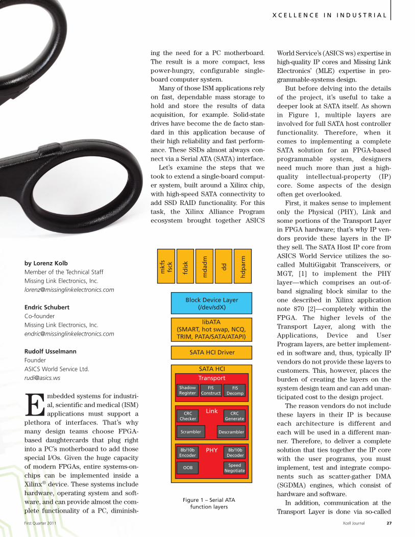
But before delving into the detailsof the project, it’s useful to take adeeper look at SATA itself. As shownin Figure 1, multiple layers areinvolved for full SATA host controllerfunctionality. Therefore, when itcomes to implementing a completeSATA solution for an FPGA-basedprogrammable system, designersneed much more than just a high-quality intellectual-property (IP)core. Some aspects of the designoften get overlooked.
First, it makes sense to implementonly the Physical (PHY), Link andsome portions of the Transport Layerin FPGA hardware; that’s why IP ven-dors provide these layers in the IPthey sell. The SATA Host IP core fromASICS World Service utilizes the so-called MultiGigabit Transceivers, orMGT, [1] to implement the PHYlayer—which comprises an out-of-band signaling block similar to theone described in Xilinx applicationnote 870 [2]—completely within theFPGA. The higher levels of theTransport Layer, along with theApplications, Device and UserProgram layers, are better implement-ed in software and, thus, typically IPvendors do not provide these layers tocustomers. This, however, places theburden of creating the layers on thesystem design team and can add unan-ticipated cost to the design project.
The reason vendors do not includethese layers in their IP is becauseeach architecture is different andeach will be used in a different man-ner. Therefore, to deliver a completesolution that ties together the IP corewith the user programs, you mustimplement, test and integrate compo-nents such as scatter-gather DMA(SGDMA) engines, which consist ofhardware and software.
In addition, communication at theTransport Layer is done via so-called
by Lorenz KolbMember of the Technical StaffMissing Link Electronics, [email protected]
Endric SchubertCo-founder Missing Link Electronics, [email protected]
Rudolf UsselmannFounder ASICS World Service [email protected]
mkf
sfs
ck
fdis
k
md
adm
dd
hd
par
m
Block Device Layer(/dev/sdX)
libATA(SMART, hot swap, NCQ,TRIM, PATA/SATA/ATAPI)
SATA HCI Driver
SATA HCI
Transport
Link
PHY
ShadowRegister
FISConstruct
FISDecomp
CRCChecker
CRCGenerate
Scrambler Descrambler
8b/10bEncoder
8b/10bDecoder
OOB SpeedNegotiate
Figure 1 – Serial ATA function layers
X C E L L E N C E I N I N D U S T R I A L
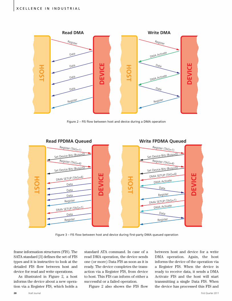
frame information structures (FIS). TheSATA standard [3] defines the set of FIStypes and it is instructive to look at thedetailed FIS flow between host anddevice for read and write operations.
As illustrated in Figure 2, a hostinforms the device about a new opera-tion via a Register FIS, which holds a
standard ATA command. In case of aread DMA operation, the device sendsone (or more) Data FIS as soon as it isready. The device completes the trans-action via a Register FIS, from deviceto host. This FIS can inform of either asuccessful or a failed operation.
Figure 2 also shows the FIS flow
between host and device for a writeDMA operation. Again, the hostinforms the device of the operation viaa Register FIS. When the device isready to receive data, it sends a DMAActivate FIS and the host will starttransmitting a single Data FIS. Whenthe device has processed this FIS and
28 Xcell Journal First Quarter 2011
X C E L L E N C E I N I N D U S T R I A L
HO
ST
Read DMA Write DMA
DEV
ICE
DEV
ICEH
OST
RegisterRegister
Data
Data
Data
Data
DMA Activate
DMA Activate
Data
Data
RegisterRegister
HO
ST
HO
ST
Read FPDMA Queued Write FPDMA Queued
DEV
ICE
DEV
ICE
DataData
Data
Data
Register
Register
Register RegisterData
DataDMA SETUP (TAG=4) DMA SETUP (TAG=4)
Set Device Bits (Busy=0)
Register (TAG=1)
Register (TAG=4)
Set Device Bits (Busy=0)
Set Device Bits (Busy=0)
Register (TAG=1)
Register (TAG=4)
Set Device Bits (Busy=0)
DMA SETUP (TAG=1)
DMA SETUP (TAG=1)
DMA Activate
DMA Activate
Figure 2 – FIS flow between host and device during a DMA operation
Figure 3 – FIS flow between host and device during first-party DMA queued operation
it still expects data, it again sends aDMA Activate FIS. The process iscompleted in the same way as the readDMA operation.
A new feature introduced withSATA and not found in parallel ATA isthe so-called first-party DMA. Thisfeature transfers some control overthe DMA engine to the device. In thisway the device can cache a list ofcommands and reorder them for opti-mized performance, a techniquecalled native command queuing. NewATA commands are used for first-party DMA transfers. Because thedevice does not necessarily completethese commands instantaneously, but
rather queues them, the FIS flow is abit different for this mode of opera-tion. The flow for a read first-partyDMA queued command is shown onthe left side of Figure 3.
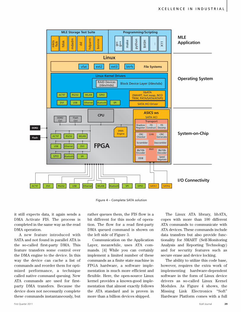
Communication on the ApplicationLayer, meanwhile, uses ATA com-mands. [4] While you can certainlyimplement a limited number of thesecommands as a finite state machine inFPGA hardware, a software imple-mentation is much more efficient andflexible. Here, the open-source Linuxkernel provides a known-good imple-mentation that almost exactly followsthe ATA standard and is proven inmore than a billion devices shipped.
The Linux ATA library, libATA,copes with more than 100 differentATA commands to communicate withATA devices. These commands includedata transfers but also provide func-tionality for SMART (Self-MonitoringAnalysis and Reporting Technology)and for security features such assecure erase and device locking.
The ability to utilize this code base,however, requires the extra work ofimplementing hardware-dependentsoftware in the form of Linux devicedrivers as so-called Linux KernelModules. As Figure 4 shows, theMissing Link Electronics “Soft”Hardware Platform comes with a full
First Quarter 2011 Xcell Journal 29
X C E L L E N C E I N I N D U S T R I A L
MLE Storage Test Suite
File Systems
Linux
Programming/Scripting
mkt
sfs
ck
fdis
k
md
adm
dd
hd
par
m
bo
nn
ie
gcc
g+
+
mak
e
pyt
ho
n
BA
SH ... X11
vfat
Linux Kernel Drivers
ext2 ext3 btrfs
RAID Devices(/dev/mdx) Block Device Layer (/dev/sdx)
libATA(SMART, hot swap, NCOTRIM, PATA/SATA/ATAPI)
SATA HCI Driver
AC’97
AC’97
DDR2
Flash
DVI RS232 USB Ethernet WLAN Bluetooth SPI GPIO SATA1 SATA2
RS232 WLAN
AC’97 RS232 WLAN
GPIO
GPIO
DVI USB Ethernet
DVIUSB Ethernet
SPIBluetooth
SPIBluetooth
DDR2Ctrl
FlashCtrl
DMAEngine
CPUASICS ws
FPGA
MLEApplication
Operating System
System-on-Chip
I/O Connectivity
ShadowRegister
CRCChecker
8b/10bEncoder
8b/10bDecoder
SpeedNegotiateODB
Scrambler Descrambler
CRCGenerate
FISConstruct
FISDecomp
SATA HCITransport
Link
PHY
Figure 4 – Complete SATA solution
GNU/Linux software stack prein-stalled, along with a tested and opti-mized device driver for the SATA hostIP core from ASICS World Service.
When integrating a SATA IP core intoan FPGA-based system, there are manydegrees of freedom. So, pushing the lim-its of the whole system requires knowl-edge of not just software or hardware,but both. Integration must proceed intandem for software and hardware.
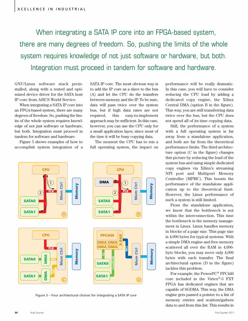
Figure 5 shows examples of how toaccomplish system integration of a
SATA IP core. The most obvious way isto add the IP core as a slave to the bus(A) and let the CPU do the transfersbetween memory and the IP. To be sure,data will pass twice over the systembus, but if high data rates are notrequired, this easy-to-implementapproach may be sufficient. In this case,however, you can use the CPU only fora small application layer, since most ofthe time it will be busy copying data.
The moment the CPU has to run afull operating system, the impact on
performance will be really dramatic.In this case, you will have to considerreducing the CPU load by adding adedicated copy engine, the XilinxCentral DMA (option B in the figure).This way, you are still transferring datatwice over the bus, but the CPU doesnot spend all of its time copying data.
Still, the performance of a systemwith a full operating system is faraway from a standalone application,and both are far from the theoreticalperformance limits. The third architec-ture option (C in the figure) changesthis picture by reducing the load of thesystem bus and using simple dedicatedcopy engines via Xilinx’s streamingNPI port and Multiport MemoryController (MPMC). This boosts theperformance of the standalone appli-cation up to the theoretical limit.However, the Linux performance ofsuch a system is still limited.
From the standalone application,we know that the bottleneck is notwithin the interconnection. This timethe bottleneck is the memory manage-ment in Linux. Linux handles memoryin blocks of a page size. This page sizeis 4,096 bytes for typical systems. Witha simple DMA engine and free memoryscattered all over the RAM in 4,096-byte blocks, you may move only 4,096bytes with each transfer. The finalarchitectural option (D in the figure)tackles this problem.
For example, the PowerPC® PPC440core included in the Virtex®-5 FXTFPGA has dedicated engines that arecapable of SGDMA. This way, the DMAengine gets passed a pointer to a list ofmemory entries and scatters/gathersdata to and from this list. This results in
30 Xcell Journal First Quarter 2011
X C E L L E N C E I N I N D U S T R I A L
Mem
ory
A
PLB
1
2
CPU
Mem
Ctr
l
SATA0
SATA1
Mem
ory
C
PLB
CPU
Mem
Ctr
l
Mem
ory
B
PLB
1
2
CPU
Mem
Ctr
l
SATA0
SATA1
DMA
NPI
NPI
Mem
ory
D
Mem
Ctr
lDMA DMADMA
PPC440
X-B
AR
DMA
MC
I
Loca
lLin
k
LL
SATA0
SATA1
SATA0
SATA1
DM
AD
MA
When integrating a SATA IP core into an FPGA-based system,
there are many degrees of freedom. So, pushing the limits of the whole
system requires knowledge of not just software or hardware, but both.
Integration must proceed in tandem for software and hardware.
Figure 5 – Four architectural choices for integrating a SATA IP core
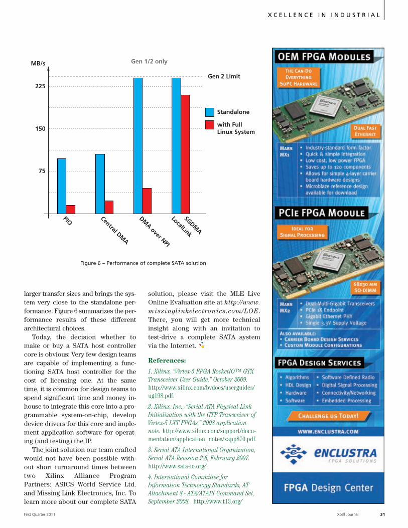
larger transfer sizes and brings the sys-tem very close to the standalone per-formance. Figure 6 summarizes the per-formance results of these differentarchitectural choices.
Today, the decision whether tomake or buy a SATA host controllercore is obvious: Very few design teamsare capable of implementing a func-tioning SATA host controller for thecost of licensing one. At the sametime, it is common for design teams tospend significant time and money in-house to integrate this core into a pro-grammable system-on-chip, developdevice drivers for this core and imple-ment application software for operat-ing (and testing) the IP.
The joint solution our team craftedwould not have been possible with-out short turnaround times betweentwo Xilinx Alliance ProgramPartners: ASICS World Service Ltd.and Missing Link Electronics, Inc. Tolearn more about our complete SATA
solution, please visit the MLE LiveOnline Evaluation site at http://www.
missinglinkelectronics.com/LOE.There, you will get more technicalinsight along with an invitation totest-drive a complete SATA systemvia the Internet.
References:
1. Xilinx, “Virtex-5 FPGA RocketIO™ GTXTransceiver User Guide,” October 2009.http://www.xilinx.com/bvdocs/userguides/ug198.pdf.
2. Xilinx, Inc., “Serial ATA Physical LinkInitialization with the GTP Transceiver ofVirtex-5 LXT FPGAs,” 2008 applicationnote. http://www.xilinx.com/support/docu-mentation/application_notes/xapp870.pdf.
3. Serial ATA International Organization,Serial ATA Revision 2.6, February 2007.http://www.sata-io.org/
4. International Committee forInformation Technology Standards, ATAttachment 8 - ATA/ATAPI Command Set,September 2008. http://www.t13.org/
First Quarter 2011 Xcell Journal 31
X C E L L E N C E I N I N D U S T R I A L
MB/s
225
150
75
PIO Central DMA
DMA over NPI
LocalLink
SGDMA
Gen 1/2 only
Gen 2 Limit
with FullLinux System
Standalone
Figure 6 – Performance of complete SATA solution