xilinx 7 series libraries guide for schematic designs
TRANSCRIPT

Xilinx 7 Series FPGA LibrariesGuide for Schematic Designs
UG799 (v 13.1) March 1, 2011

Xilinx is disclosing this user guide, manual, release note, and/or specification (the “Documentation”) to yousolely for use in the development of designs to operate with Xilinx hardware devices. You may not reproduce,distribute, republish, download, display, post, or transmit the Documentation in any form or by any meansincluding, but not limited to, electronic, mechanical, photocopying, recording, or otherwise, without the priorwritten consent of Xilinx. Xilinx expressly disclaims any liability arising out of your use of the Documentation.Xilinx reserves the right, at its sole discretion, to change the Documentation without notice at any time. Xilinxassumes no obligation to correct any errors contained in the Documentation, or to advise you of any correctionsor updates. Xilinx expressly disclaims any liability in connection with technical support or assistance that may beprovided to you in connection with the Information.
THE DOCUMENTATION IS DISCLOSED TO YOU “AS-IS” WITH NOWARRANTY OF ANY KIND. XILINXMAKES NO OTHER WARRANTIES, WHETHER EXPRESS, IMPLIED, OR STATUTORY, REGARDINGTHE DOCUMENTATION, INCLUDING ANY WARRANTIES OF MERCHANTABILITY, FITNESS FOR APARTICULAR PURPOSE, OR NONINFRINGEMENT OF THIRD-PARTY RIGHTS. IN NO EVENT WILLXILINX BE LIABLE FOR ANY CONSEQUENTIAL, INDIRECT, EXEMPLARY, SPECIAL, OR INCIDENTALDAMAGES, INCLUDING ANY LOSS OF DATA OR LOST PROFITS, ARISING FROM YOUR USE OF THEDOCUMENTATION.
© Copyright 2002-2011 Xilinx Inc. All Rights Reserved. XILINX, the Xilinx logo, the Brand Window and otherdesignated brands included herein are trademarks of Xilinx, Inc. All other trademarks are the property oftheir respective owners.
Xilinx 7 Series FPGA Libraries Guide for Schematic Designs2 www.xilinx.com UG799 (v 13.1) March 1, 2011

Chapter 1
IntroductionThis schematic guide is part of the ISE documentation collection. A separate version ofthis guide is available if you prefer to work with HDL.
This guide contains the following:
• Introduction.
• A list of design elements supported in this architecture, organized by functionalcategories.
• Individual descriptions of each available primitive.
About Design ElementsThis version of the Libraries Guide describes design elements available for thisarchitecture. There are several categories of design elements:
• Primitives - The simplest design elements in the Xilinx libraries. Primitives are thedesign element "atoms." Examples of Xilinx primitives are the simple buffer, BUF,and the D flip-flop with clock enable and clear, FDCE.
• Macros - The design element "molecules" of the Xilinx libraries. Macros can becreated from the design element primitives or macros. For example, the FD4CEflip-flop macro is a composite of 4 FDCE primitives.
Xilinx maintains software libraries with hundreds of functional design elements(macros and primitives) for different device architectures. New functional elements areassembled with each release of development system software. This guide is one ina series of architecture-specific libraries.
Xilinx 7 Series FPGA Libraries Guide for Schematic DesignsUG799 (v 13.1) March 1, 2011 www.xilinx.com 3

Xilinx 7 Series FPGA Libraries Guide for Schematic Designs4 www.xilinx.com UG799 (v 13.1) March 1, 2011

Chapter 2
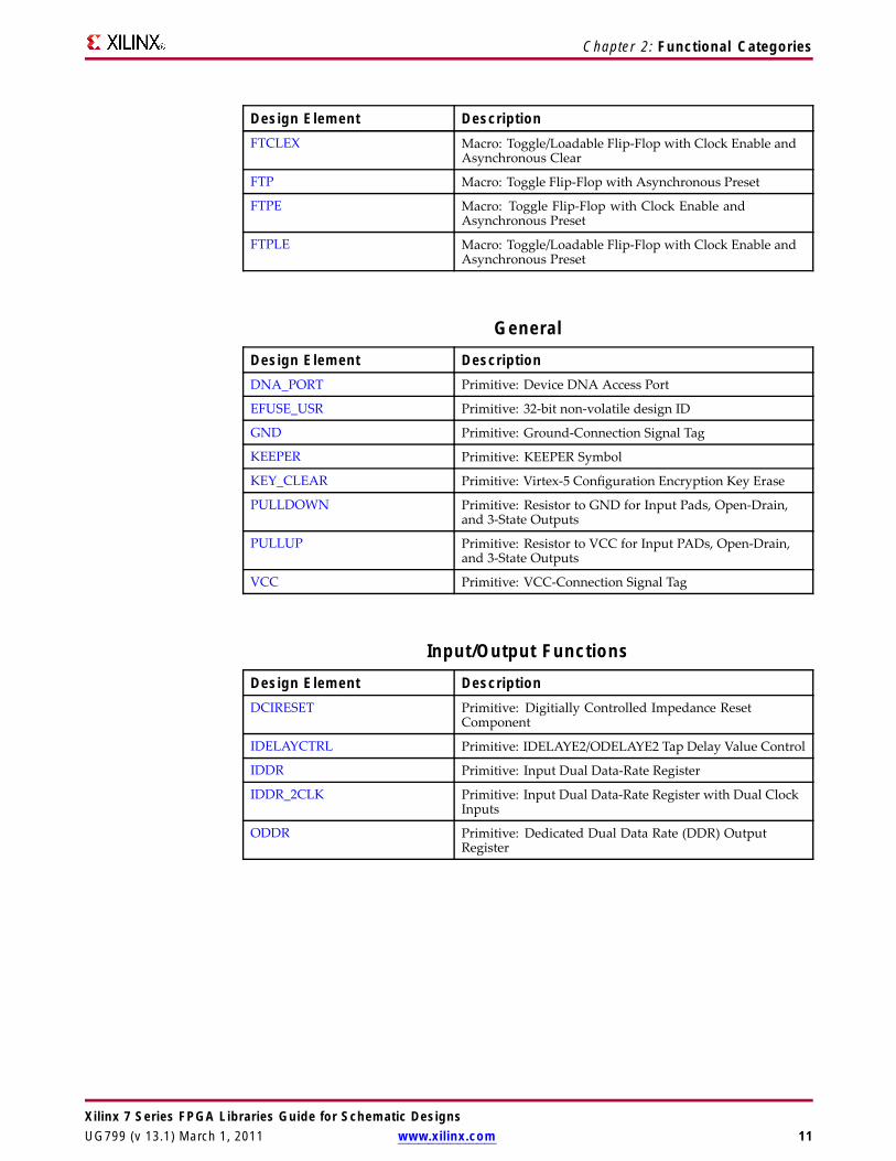
Functional CategoriesThis section categorizes, by function, the circuit design elements described in detail laterin this guide. The elements ( primitives and macros) are listed in alphanumeric orderunder each functional category.
Arithmetic General Memory
Buffer Input/Output Functions Mux
Carry Logic IO Shift Register
Clocking Resources IO FlipFlop Shifter
Comparator IO Latch
Counter Latch
Decoder Logic
Flip Flop LUT
Xilinx 7 Series FPGA Libraries Guide for Schematic DesignsUG799 (v 13.1) March 1, 2011 www.xilinx.com 5

Chapter 2: Functional Categories
ArithmeticDesign Element DescriptionACC16 Macro: 16-Bit Loadable Cascadable Accumulator with
Carry-In, Carry-Out, and Synchronous Reset
ACC4 Macro: 4-Bit Loadable Cascadable Accumulator withCarry-In, Carry-Out, and Synchronous Reset
ACC8 Macro: 8-Bit Loadable Cascadable Accumulator withCarry-In, Carry-Out, and Synchronous Reset
ADD16 Macro: 16-Bit Cascadable Full Adder with Carry-In,Carry-Out, and Overflow
ADD4 Macro: 4-Bit Cascadable Full Adder with Carry-In,Carry-Out, and Overflow
ADD8 Macro: 8-Bit Cascadable Full Adder with Carry-In,Carry-Out, and Overflow
ADSU16 Macro: 16-Bit Cascadable Adder/Subtracter with Carry-In,Carry-Out, and Overflow
ADSU4 Macro: 4-Bit Cascadable Adder/Subtracter with Carry-In,Carry-Out, and Overflow
ADSU8 Macro: 8-Bit Cascadable Adder/Subtracter with Carry-In,Carry-Out, and Overflow
DSP48E1 Primitive: 48-bit Multi-Functional Arithmetic Block
MULT18X18 Primitive: 18 x 18 Signed Multiplier
MULT18X18S Primitive: 18 x 18 Signed Multiplier -- Registered Version
BufferDesign Element DescriptionBUF Primitive: General Purpose Buffer
BUFCF Primitive: Fast Connect Buffer
BUFG Global Clock Buffer
BUFGCE Primitive: Global Clock Buffer with Clock Enable
BUFGCE_1 Primitive: Global Clock Buffer with Clock Enable andOutput State 1
BUFGMUX_CTRL Primitive: 2-to-1 Global Clock MUX Buffer
BUFGP Primitive: Primary Global Buffer for Driving Clocks
Xilinx 7 Series FPGA Libraries Guide for Schematic Designs6 www.xilinx.com UG799 (v 13.1) March 1, 2011

Chapter 2: Functional Categories
Carry LogicDesign Element DescriptionCARRY4 Primitive: Fast Carry Logic with Look Ahead
MUXCY Primitive: 2-to-1 Multiplexer for Carry Logic with GeneralOutput
MUXCY_D Primitive: 2-to-1 Multiplexer for Carry Logic with DualOutput
MUXCY_L Primitive: 2-to-1 Multiplexer for Carry Logic with LocalOutput
XORCY Primitive: XOR for Carry Logic with General Output
Clocking ResourcesDesign Element DescriptionBUFGCTRL Primitive: Global Clock MUX Buffer
BUFH Primitive: Clock buffer for a single clocking region
BUFHCE Primitive: HROW Clock Buffer for a Single ClockingRegion with Clock Enable
BUFIO Primitive: Local Clock Buffer for I/O
BUFIODQS Primitive: Differential Clock Input for TransceiverReference Clocks
BUFR Primitive: Regional Clock Buffer for I/O and LogicResources within a Clock Region
ComparatorDesign Element DescriptionCOMP16 Macro: 16-Bit Identity Comparator
COMP2 Macro: 2-Bit Identity Comparator
COMP4 Macro: 4-Bit Identity Comparator
COMP8 Macro: 8-Bit Identity Comparator
COMPM16 Macro: 16-Bit Magnitude Comparator
COMPM2 Macro: 2-Bit Magnitude Comparator
COMPM4 Macro: 4-Bit Magnitude Comparator
COMPM8 Macro: 8-Bit Magnitude Comparator
COMPMC16 Macro: 16-Bit Magnitude Comparator
COMPMC8 Macro: 8-Bit Magnitude Comparator
CounterDesign Element DescriptionCB16CE Macro: 16-Bit Cascadable Binary Counter with Clock
Enable and Asynchronous Clear
Xilinx 7 Series FPGA Libraries Guide for Schematic DesignsUG799 (v 13.1) March 1, 2011 www.xilinx.com 7

Chapter 2: Functional Categories
Design Element DescriptionCB16CLE Macro: 16-Bit Loadable Cascadable Binary Counters with
Clock Enable and Asynchronous Clear
CB16CLED Macro: 16-Bit Loadable Cascadable Bidirectional BinaryCounters with Clock Enable and Asynchronous Clear
CB16RE Macro: 16-Bit Cascadable Binary Counter with ClockEnable and Synchronous Reset
CB2CE Macro: 2-Bit Cascadable Binary Counter with Clock Enableand Asynchronous Clear
CB2CLE Macro: 2-Bit Loadable Cascadable Binary Counters withClock Enable and Asynchronous Clear
CB2CLED Macro: 2-Bit Loadable Cascadable Bidirectional BinaryCounters with Clock Enable and Asynchronous Clear
CB2RE Macro: 2-Bit Cascadable Binary Counter with Clock Enableand Synchronous Reset
CB4CE Macro: 4-Bit Cascadable Binary Counter with Clock Enableand Asynchronous Clear
CB4CLE Macro: 4-Bit Loadable Cascadable Binary Counters withClock Enable and Asynchronous Clear
CB4CLED Macro: 4-Bit Loadable Cascadable Bidirectional BinaryCounters with Clock Enable and Asynchronous Clear
CB4RE Macro: 4-Bit Cascadable Binary Counter with Clock Enableand Synchronous Reset
CB8CE Macro: 8-Bit Cascadable Binary Counter with Clock Enableand Asynchronous Clear
CB8CLE Macro: 8-Bit Loadable Cascadable Binary Counters withClock Enable and Asynchronous Clear
CB8CLED Macro: 8-Bit Loadable Cascadable Bidirectional BinaryCounters with Clock Enable and Asynchronous Clear
CB8RE Macro: 8-Bit Cascadable Binary Counter with Clock Enableand Synchronous Reset
CC16CE Macro: 16-Bit Cascadable Binary Counter with ClockEnable and Asynchronous Clear
CC16CLE Macro: 16-Bit Loadable Cascadable Binary Counter withClock Enable and Asynchronous Clear
CC16CLED Macro: 16-Bit Loadable Cascadable Bidirectional BinaryCounter with Clock Enable and Asynchronous Clear
CC16RE Macro: 16-Bit Cascadable Binary Counter with ClockEnable and Synchronous Reset
CC8CE Macro: 8-Bit Cascadable Binary Counter with Clock Enableand Asynchronous Clear
CC8CLE Macro: 8-Bit Loadable Cascadable Binary Counter withClock Enable and Asynchronous Clear
CC8CLED Macro: 8-Bit Loadable Cascadable Bidirectional BinaryCounter with Clock Enable and Asynchronous Clear
CC8RE Macro: 8-Bit Cascadable Binary Counter with Clock Enableand Synchronous Reset
CD4CE Macro: 4-Bit Cascadable BCD Counter with Clock Enableand Asynchronous Clear
Xilinx 7 Series FPGA Libraries Guide for Schematic Designs8 www.xilinx.com UG799 (v 13.1) March 1, 2011

Chapter 2: Functional Categories
Design Element DescriptionCD4CLE Macro: 4-Bit Loadable Cascadable BCD Counter with
Clock Enable and Asynchronous Clear
CD4RE Macro: 4-Bit Cascadable BCD Counter with Clock Enableand Synchronous Reset
CD4RLE Macro: 4-Bit Loadable Cascadable BCD Counter withClock Enable and Synchronous Reset
CJ4CE Macro: 4-Bit Johnson Counter with Clock Enable andAsynchronous Clear
CJ4RE Macro: 4-Bit Johnson Counter with Clock Enable andSynchronous Reset
CJ5CE Macro: 5-Bit Johnson Counter with Clock Enable andAsynchronous Clear
CJ5RE Macro: 5-Bit Johnson Counter with Clock Enable andSynchronous Reset
CJ8CE Macro: 8-Bit Johnson Counter with Clock Enable andAsynchronous Clear
CJ8RE Macro: 8-Bit Johnson Counter with Clock Enable andSynchronous Reset
DecoderDesign Element DescriptionD2_4E Macro: 2- to 4-Line Decoder/Demultiplexer with Enable
D3_8E Macro: 3- to 8-Line Decoder/Demultiplexer with Enable
D4_16E Macro: 4- to 16-Line Decoder/Demultiplexer with Enable
DEC_CC16 Macro: 16-Bit Active Low Decoder
DEC_CC4 Macro: 4-Bit Active Low Decoder
DEC_CC8 Macro: 8-Bit Active Low Decoder
Flip FlopDesign Element DescriptionFD Unknown type: D Flip-Flop
FD_1 Primitive: D Flip-Flop with Negative-Edge Clock
FD16CE Macro: 16-Bit Data Register with Clock Enable andAsynchronous Clear
FD16RE Macro: 16-Bit Data Register with Clock Enable andSynchronous Reset
FD4CE Macro: 4-Bit Data Register with Clock Enable andAsynchronous Clear
FD4RE Macro: 4-Bit Data Register with Clock Enable andSynchronous Reset
FD8CE Macro: 8-Bit Data Register with Clock Enable andAsynchronous Clear
Xilinx 7 Series FPGA Libraries Guide for Schematic DesignsUG799 (v 13.1) March 1, 2011 www.xilinx.com 9

Chapter 2: Functional Categories
Design Element DescriptionFD8RE Macro: 8-Bit Data Register with Clock Enable and
Synchronous Reset
FDC Unknown type: D Flip-Flop with Asynchronous Clear
FDC_1 Primitive: D Flip-Flop with Negative-Edge Clock andAsynchronous Clear
FDCE Primitive: D Flip-Flop with Clock Enable andAsynchronous Clear
FDCE_1 Primitive: D Flip-Flop with Negative-Edge Clock, ClockEnable, and Asynchronous Clear
FDE Primitive: D Flip-Flop with Clock Enable
FDE_1 Primitive: D Flip-Flop with Negative-Edge Clock andClock Enable
FDP Unknown type: D Flip-Flop with Asynchronous Preset
FDP_1 Primitive: D Flip-Flop with Negative-Edge Clock andAsynchronous Preset
FDPE Primitive: D Flip-Flop with Clock Enable andAsynchronous Preset
FDPE_1 Primitive: D Flip-Flop with Negative-Edge Clock, ClockEnable, and Asynchronous Preset
FDR Unknown type: D Flip-Flop with Synchronous Reset
FDR_1 Primitive: D Flip-Flop with Negative-Edge Clock andSynchronous Reset
FDRE Primitive: D Flip-Flop with Clock Enable and SynchronousReset
FDRE_1 Primitive: D Flip-Flop with Negative-Clock Edge, ClockEnable, and Synchronous Reset
FDS Unknown type: D Flip-Flop with Synchronous Set
FDS_1 Primitive: D Flip-Flop with Negative-Edge Clock andSynchronous Set
FDSE Primitive: D Flip-Flop with Clock Enable and SynchronousSet
FDSE_1 Primitive: D Flip-Flop with Negative-Edge Clock, ClockEnable, and Synchronous Set
FJKC Macro: J-K Flip-Flop with Asynchronous Clear
FJKCE Macro: J-K Flip-Flop with Clock Enable and AsynchronousClear
FJKP Macro: J-K Flip-Flop with Asynchronous Preset
FJKPE Macro: J-K Flip-Flop with Clock Enable and AsynchronousPreset
FTC Macro: Toggle Flip-Flop with Asynchronous Clear
FTCE Macro: Toggle Flip-Flop with Clock Enable andAsynchronous Clear
FTCLE Macro: Toggle/Loadable Flip-Flop with Clock Enable andAsynchronous Clear
Xilinx 7 Series FPGA Libraries Guide for Schematic Designs10 www.xilinx.com UG799 (v 13.1) March 1, 2011
Chapter 2: Functional Categories
Design Element DescriptionFTCLEX Macro: Toggle/Loadable Flip-Flop with Clock Enable and
Asynchronous Clear
FTP Macro: Toggle Flip-Flop with Asynchronous Preset
FTPE Macro: Toggle Flip-Flop with Clock Enable andAsynchronous Preset
FTPLE Macro: Toggle/Loadable Flip-Flop with Clock Enable andAsynchronous Preset
GeneralDesign Element DescriptionDNA_PORT Primitive: Device DNA Access Port
EFUSE_USR Primitive: 32-bit non-volatile design ID
GND Primitive: Ground-Connection Signal Tag
KEEPER Primitive: KEEPER Symbol
KEY_CLEAR Primitive: Virtex-5 Configuration Encryption Key Erase
PULLDOWN Primitive: Resistor to GND for Input Pads, Open-Drain,and 3-State Outputs
PULLUP Primitive: Resistor to VCC for Input PADs, Open-Drain,and 3-State Outputs
VCC Primitive: VCC-Connection Signal Tag
Input/Output FunctionsDesign Element DescriptionDCIRESET Primitive: Digitially Controlled Impedance Reset
Component
IDELAYCTRL Primitive: IDELAYE2/ODELAYE2 Tap Delay Value Control
IDDR Primitive: Input Dual Data-Rate Register
IDDR_2CLK Primitive: Input Dual Data-Rate Register with Dual ClockInputs
ODDR Primitive: Dedicated Dual Data Rate (DDR) OutputRegister
Xilinx 7 Series FPGA Libraries Guide for Schematic DesignsUG799 (v 13.1) March 1, 2011 www.xilinx.com 11

Chapter 2: Functional Categories
IODesign Element DescriptionIBUF Primitive: Input Buffer
IBUFDS Primitive: Differential Signaling Input Buffer
IBUFDS_DIFF_OUT Primitive: 7 series JTAG Boundary Scan Logic ControlCircuit
IBUF16 Macro: 16-Bit Input Buffer
IBUF4 Macro: 4-Bit Input Buffer
IBUF8 Macro: 8-Bit Input Buffer
IBUFG Primitive: Dedicated Input Clock Buffer
IBUFGDS Primitive: Differential Signaling Dedicated Input ClockBuffer and Optional Delay
IBUFGDS_DIFF_OUT Primitive: Differential Signaling Input Buffer withDifferential Output
IOBUF Primitive: Bi-Directional Buffer
IOBUFDS Primitive: 3-State Differential Signaling I/O Buffer withActive Low Output Enable
OBUF Primitive: Output Buffer
OBUFDS Primitive: Differential Signaling Output Buffer
OBUF16 Macro: 16-Bit Output Buffer
OBUF4 Macro: 4-Bit Output Buffer
OBUF8 Macro: 8-Bit Output Buffer
OBUFT Primitive: 3-State Output Buffer with Active Low OutputEnable
OBUFTDS Primitive: 3-State Output Buffer with Differential Signaling,Active-Low Output Enable
OBUFT16 Macro: 16-Bit 3-State Output Buffer with Active LowOutput Enable
OBUFT4 Macro: 4-Bit 3-State Output Buffers with Active-LowOutput Enable
OBUFT8 Macro: 8-Bit 3-State Output Buffers with Active-LowOutput Enable
IO FlipFlopDesign Element DescriptionIFD Macro: Input D Flip-Flop
IFD_1 Macro: Input D Flip-Flop with Inverted Clock(Asynchronous Preset)
IFD16 Macro: 16-Bit Input D Flip-Flop
IFD4 Macro: 4-Bit Input D Flip-Flop
IFD8 Macro: 8-Bit Input D Flip-Flop
IFDI Macro: Input D Flip-Flop (Asynchronous Preset)
Xilinx 7 Series FPGA Libraries Guide for Schematic Designs12 www.xilinx.com UG799 (v 13.1) March 1, 2011

Chapter 2: Functional Categories
Design Element DescriptionIFDI_1 Macro: Input D Flip-Flop with Inverted Clock
(Asynchronous Preset)
IFDX Macro: Input D Flip-Flop with Clock Enable
IFDX_1 Macro: Input D Flip-Flop with Inverted Clock and ClockEnable
IFDX16 Macro: 16-Bit Input D Flip-Flops with Clock Enable
IFDX4 Macro: 4-Bit Input D Flip-Flop with Clock Enable
IFDX8 Macro: 8-Bit Input D Flip-Flop with Clock Enable
OFD Macro: Output D Flip-Flop
OFD_1 Macro: Output D Flip-Flop with Inverted Clock
OFD16 Macro: 16-Bit Output D Flip-Flop
OFD4 Macro: 4-Bit Output D Flip-Flop
OFD8 Macro: 8-Bit Output D Flip-Flop
OFDE Macro: D Flip-Flop with Active-High Enable OutputBuffers
OFDE_1 Macro: D Flip-Flop with Active-High Enable Output Bufferand Inverted Clock
OFDE4 Macro: 4-Bit D Flip-Flop with Active-High Enable OutputBuffers
OFDE8 Macro: 8-Bit D Flip-Flop with Active-High Enable OutputBuffers
OFDE16 Macro: 16-Bit D Flip-Flop with Active-High Enable OutputBuffers
OFDI Macro: Output D Flip-Flop (Asynchronous Preset)
OFDI_1 Macro: Output D Flip-Flop with Inverted Clock(Asynchronous Preset)
OFDT Macro: D Flip-Flop with Active-Low 3-State Output Buffer
OFDT_1 Macro: D Flip-Flop with Active-Low 3-State Output Bufferand Inverted Clock
OFDT16 Macro: 16-Bit D Flip-Flop with Active-Low 3-State OutputBuffers
OFDT4 Macro: 4-Bit D Flip-Flop with Active-Low 3-State OutputBuffers
OFDT8 Macro: 8-Bit D Flip-Flop with Active-Low 3-State OutputBuffers
OFDX Macro: Output D Flip-Flop with Clock Enable
OFDX_1 Macro: Output D Flip-Flop with Inverted Clock and ClockEnable
OFDX16 Macro: 16-Bit Output D Flip-Flop with Clock Enable
OFDX4 Macro: 4-Bit Output D Flip-Flop with Clock Enable
OFDX8 Macro: 8-Bit Output D Flip-Flop with Clock Enable
OFDXI Macro: Output D Flip-Flop with Clock Enable(Asynchronous Preset)
Xilinx 7 Series FPGA Libraries Guide for Schematic DesignsUG799 (v 13.1) March 1, 2011 www.xilinx.com 13

Chapter 2: Functional Categories
Design Element DescriptionOFDXI_1 Macro: Output D Flip-Flop with Inverted Clock and Clock
Enable (Asynchronous Preset)
IO LatchDesign Element DescriptionILD Macro: Transparent Input Data Latch
ILD_1 Macro: Transparent Input Data Latch with Inverted Gate
ILD16 Macro: Transparent Input Data Latch
ILD4 Macro: Transparent Input Data Latch
ILD8 Macro: Transparent Input Data Latch
ILDI Macro: Transparent Input Data Latch (AsynchronousPreset)
ILDI_1 Macro: Transparent Input Data Latch with Inverted Gate(Asynchronous Preset)
ILDXI Macro: Transparent Input Data Latch (AsynchronousPreset)
ILDXI_1 Macro: Transparent Input Data Latch with Inverted Gate(Asynchronous Preset)
LatchDesign Element DescriptionILD Macro: Transparent Input Data Latch
ILD_1 Macro: Transparent Input Data Latch with Inverted Gate
ILD16 Macro: Transparent Input Data Latch
ILD4 Macro: Transparent Input Data Latch
ILD8 Macro: Transparent Input Data Latch
ILDI Macro: Transparent Input Data Latch (AsynchronousPreset)
ILDI_1 Macro: Transparent Input Data Latch with Inverted Gate(Asynchronous Preset)
ILDXI Macro: Transparent Input Data Latch (AsynchronousPreset)
ILDXI_1 Macro: Transparent Input Data Latch with Inverted Gate(Asynchronous Preset)
Xilinx 7 Series FPGA Libraries Guide for Schematic Designs14 www.xilinx.com UG799 (v 13.1) March 1, 2011

Chapter 2: Functional Categories
LogicDesign Element DescriptionCARRY4 Primitive: Fast Carry Logic with Look Ahead
MUXCY Primitive: 2-to-1 Multiplexer for Carry Logic with GeneralOutput
MUXCY_D Primitive: 2-to-1 Multiplexer for Carry Logic with DualOutput
MUXCY_L Primitive: 2-to-1 Multiplexer for Carry Logic with LocalOutput
XORCY Primitive: XOR for Carry Logic with General Output
LUTDesign Element DescriptionCFGLUT5 Primitive: 5-input Dynamically Reconfigurable Look-Up
Table (LUT)
LUT1 Primitive: 1-Bit Look-Up Table with General Output
LUT1_D Primitive: 1-Bit Look-Up Table with Dual Output
LUT1_L Primitive: 1-Bit Look-Up Table with Local Output
LUT2 Primitive: 2-Bit Look-Up Table with General Output
LUT2_D Primitive: 2-Bit Look-Up Table with Dual Output
LUT2_L Primitive: 2-Bit Look-Up Table with Local Output
LUT3 Primitive: 3-Bit Look-Up Table with General Output
LUT3_D Primitive: 3-Bit Look-Up Table with Dual Output
LUT3_L Primitive: 3-Bit Look-Up Table with Local Output
LUT4 Primitive: 4-Bit Look-Up-Table with General Output
LUT4_D Primitive: 4-Bit Look-Up Table with Dual Output
LUT4_L Primitive: 4-Bit Look-Up Table with Local Output
LUT5 Primitive: 5-Input Lookup Table with General Output
LUT5_D Primitive: 5-Input Lookup Table with General and LocalOutputs
LUT5_L Primitive: 5-Input Lookup Table with Local Output
LUT6 Primitive: 6-Input Lookup Table with General Output
LUT6_D Primitive: 6-Input Lookup Table with General and LocalOutputs
LUT6_L Primitive: 6-Input Lookup Table with Local Output
LUT6_2 Primitive: Six-input, 2-output, Look-Up Table
MemoryDesign Element Description
Xilinx 7 Series FPGA Libraries Guide for Schematic DesignsUG799 (v 13.1) March 1, 2011 www.xilinx.com 15

Chapter 2: Functional Categories
Design Element DescriptionFIFO18E1 Primitive: 18KB FIFO (First In, First Out) Block RAM
Memory
FIFO36E1 Primitive: 36KB FIFO (First In, First Out) Block RAMMemory
RAMB18E1 Primitive: 18K-bit Configurable Synchronous Block RAM
RAMB36E1 Primitive: 36K-bit Configurable Synchronous Block RAM
RAM16X1D Primitive: 16-Deep by 1-Wide Static Dual Port SynchronousRAM
RAM16X1D_1 Primitive: 16-Deep by 1-Wide Static Dual Port SynchronousRAM with Negative-Edge Clock
RAM16X1S Primitive: 16-Deep by 1-Wide Static Synchronous RAM
RAM16X1S_1 Primitive: 16-Deep by 1-Wide Static Synchronous RAMwith Negative-Edge Clock
RAM16X2S Primitive: 16-Deep by 2-Wide Static Synchronous RAM
RAM16X4S Primitive: 16-Deep by 4-Wide Static Synchronous RAM
RAM16X8S Primitive: 16-Deep by 8-Wide Static Synchronous RAM
RAM32M Primitive: 32-Deep by 8-bit Wide Multi Port RandomAccess Memory (Select RAM)
RAM32X1D Primitive: 32-Deep by 1-Wide Static Dual Port SynchronousRAM
RAM32X1S Primitive: 32-Deep by 1-Wide Static Synchronous RAM
RAM32X1S_1 Primitive: 32-Deep by 1-Wide Static Synchronous RAMwith Negative-Edge Clock
RAM32X2S Primitive: 32-Deep by 2-Wide Static Synchronous RAM
RAM32X4S Primitive: 32-Deep by 4-Wide Static Synchronous RAM
RAM32X8S Primitive: 32-Deep by 8-Wide Static Synchronous RAM
RAM64M Primitive: 64-Deep by 4-bit Wide Multi Port RandomAccess Memory (Select RAM)
RAM64X1D Primitive: 64-Deep by 1-Wide Dual Port Static SynchronousRAM
RAM64X1S Primitive: 64-Deep by 1-Wide Static Synchronous RAM
RAM64X1S_1 Primitive: 64-Deep by 1-Wide Static Synchronous RAMwith Negative-Edge Clock
RAM64X2S Primitive: 64-Deep by 2-Wide Static Synchronous RAM
RAM128X1D Primitive: 128-Deep by 1-Wide Dual Port Random AccessMemory (Select RAM)
RAM256X1S Primitive: 256-Deep by 1-Wide Random Access Memory(Select RAM)
ROM32X1 Primitive: 32-Deep by 1-Wide ROM
ROM64X1 Primitive: 64-Deep by 1-Wide ROM
ROM128X1 Primitive: 128-Deep by 1-Wide ROM
ROM256X1 Primitive: 256-Deep by 1-Wide ROM
Xilinx 7 Series FPGA Libraries Guide for Schematic Designs16 www.xilinx.com UG799 (v 13.1) March 1, 2011

Chapter 2: Functional Categories
MuxDesign Element DescriptionM16_1E Macro: 16-to-1 Multiplexer with Enable
M2_1 Macro: 2-to-1 Multiplexer
M2_1B1 Macro: 2-to-1 Multiplexer with D0 Inverted
M2_1B2 Macro: 2-to-1 Multiplexer with D0 and D1 Inverted
M2_1E Macro: 2-to-1 Multiplexer with Enable
M4_1E Macro: 4-to-1 Multiplexer with Enable
M8_1E Macro: 8-to-1 Multiplexer with Enable
MUXF7 Primitive: 2-to-1 Look-Up Table Multiplexer with GeneralOutput
MUXF7_D Primitive: 2-to-1 Look-Up Table Multiplexer with DualOutput
MUXF7_L Primitive: 2-to-1 look-up table Multiplexer with LocalOutput
MUXF8 Primitive: 2-to-1 Look-Up Table Multiplexer with GeneralOutput
MUXF8_D Primitive: 2-to-1 Look-Up Table Multiplexer with DualOutput
MUXF8_L Primitive: 2-to-1 Look-Up Table Multiplexer with LocalOutput
Shift RegisterDesign Element DescriptionSR16CE Macro: 16-Bit Serial-In Parallel-Out Shift Register with
Clock Enable and Asynchronous Clear
SR16CLE Macro: 16-Bit Loadable Serial/Parallel-In Parallel-Out ShiftRegister with Clock Enable and Asynchronous Clear
SR16CLED Macro: 16-Bit Shift Register with Clock Enable andAsynchronous Clear
SR16RE Macro: 16-Bit Serial-In Parallel-Out Shift Register withClock Enable and Synchronous Reset
SR16RLE Macro: 16-Bit Loadable Serial/Parallel-In Parallel-Out ShiftRegister with Clock Enable and Synchronous Reset
SR16RLED Macro: 16-Bit Shift Register with Clock Enable andSynchronous Reset
SR4CE Macro: 4-Bit Serial-In Parallel-Out Shift Register with ClockEnable and Asynchronous Clear
SR4CLE Macro: 4-Bit Loadable Serial/Parallel-In Parallel-Out ShiftRegister with Clock Enable and Asynchronous Clear
SR4CLED Macro: 4-Bit Shift Register with Clock Enable andAsynchronous Clear
SR4RE Macro: 4-Bit Serial-In Parallel-Out Shift Register with ClockEnable and Synchronous Reset
Xilinx 7 Series FPGA Libraries Guide for Schematic DesignsUG799 (v 13.1) March 1, 2011 www.xilinx.com 17

Chapter 2: Functional Categories
Design Element DescriptionSR4RLE Macro: 4-Bit Loadable Serial/Parallel-In Parallel-Out Shift
Register with Clock Enable and Synchronous Reset
SR4RLED Macro: 4-Bit Shift Register with Clock Enable andSynchronous Reset
SR8CE Macro: 8-Bit Serial-In Parallel-Out Shift Register with ClockEnable and Asynchronous Clear
SR8CLE Macro: 8-Bit Loadable Serial/Parallel-In Parallel-Out ShiftRegister with Clock Enable and Asynchronous Clear
SR8CLED Macro: 8-Bit Shift Register with Clock Enable andAsynchronous Clear
SR8RE Macro: 8-Bit Serial-In Parallel-Out Shift Register with ClockEnable and Synchronous Reset
SR8RLE Macro: 8-Bit Loadable Serial/Parallel-In Parallel-Out ShiftRegister with Clock Enable and Synchronous Reset
SR8RLED Macro: 8-Bit Shift Register with Clock Enable andSynchronous Reset
SRL16 Primitive: 16-Bit Shift Register Look-Up Table (LUT)
SRL16_1 Primitive: 16-Bit Shift Register Look-Up Table (LUT) withNegative-Edge Clock
SRL16E Primitive: 16-Bit Shift Register Look-Up Table (LUT) withClock Enable
SRL16E_1 Primitive: 16-Bit Shift Register Look-Up Table (LUT) withNegative-Edge Clock and Clock Enable
SRLC16 Primitive: 16-Bit Shift Register Look-Up Table (LUT) withCarry
SRLC16_1 Primitive: 16-Bit Shift Register Look-Up Table (LUT) withCarry and Negative-Edge Clock
SRLC16E Primitive: 16-Bit Shift Register Look-Up Table (LUT) withCarry and Clock Enable
SRLC16E_1 Primitive: 16-Bit Shift Register Look-Up Table (LUT) withCarry, Negative-Edge Clock, and Clock Enable
SRLC32E Primitive: 32 Clock Cycle, Variable Length Shift RegisterLook-Up Table (LUT) with Clock Enable
ShifterDesign Element DescriptionBRLSHFT4 Macro: 4-Bit Barrel Shifter
BRLSHFT8 Macro: 8-Bit Barrel Shifter
Xilinx 7 Series FPGA Libraries Guide for Schematic Designs18 www.xilinx.com UG799 (v 13.1) March 1, 2011

Chapter 3
About Design ElementsThis section describes the design elements that can be used with this architecture. Thedesign elements are organized alphabetically.
The following information is provided for each design element, where applicable:
• Name of element
• Brief description
• Schematic symbol (if any)
• Logic Table (if any)
• Port Descriptions (if any)
• Design Entry Method
• Available Attributes (if any)
• For more information
You can find examples of VHDL and Verilog instantiation code in the ISE software (inthe main menu, select Edit > Language Templates or in the Libraries Guide for HDLDesigns for this architecture.
Xilinx 7 Series FPGA Libraries Guide for Schematic DesignsUG799 (v 13.1) March 1, 2011 www.xilinx.com 19

Chapter 3: About Design Elements
ACC16Macro: 16-Bit Loadable Cascadable Accumulator with Carry-In, Carry-Out, andSynchronous Reset
IntroductionThis design element can add or subtract a 16-bit unsigned-binary, respectively or two’s-complement word toor from the contents of a 16-bit data register and store the results in the register. The register can be loadedwith the 16-bit word.
When the load input (L) is High, CE is ignored and the data on the D inputs is loaded into the register during theLow-to-High clock (C) transition. ACC16 loads the data on inputs D15 : D0 into the 16-bit register.
This design element operates on either 16-bit unsigned binary numbers or 16-bit two’s-complement numbers. Ifthe inputs are interpreted as unsigned binary, the result can be interpreted as unsigned binary. If the inputsare interpreted as two’s complement, the output can be interpreted as two’s complement. The only functionaldifference between an unsigned binary operation and a two’s-complement operation is how they determinewhen “overflow” occurs. Unsigned binary uses carry-out (CO), while two’s complement uses OFL to determinewhen “overflow” occurs.
• For unsigned binary operation, ACC16 can represent numbers between 0 and 15, inclusive. In add mode,CO is active (High) when the sum exceeds the bounds of the adder/subtracter. In subtract mode, CO is anactive-Low borrow-out and goes Low when the difference exceeds the bounds. The carry-out (CO) isnot registered synchronously with the data outputs. CO always reflects the accumulation of the B inputs(B15 : B0 for ACC16). This allows the cascading of ACC16s by connecting CO of one stage to CI of thenext stage. An unsigned binary “overflow” that is always active-High can be generated by gating theADD signal and CO as follows:
unsigned overflow = CO XOR ADD
Ignore OFL in unsigned binary operation.
• For two’s-complement operation, ACC16 represents numbers between -8 and +7, inclusive. If an additionor subtraction operation result exceeds this range, the OFL output goes High. The overflow (OFL) is notregistered synchronously with the data outputs. OFL always reflects the accumulation of the B inputs (B15 :B0 for ACC16) and the contents of the register, which allows cascading of ACC4s by connecting OFL of onestage to CI of the next stage.
Ignore CO in two’s-complement operation.
The synchronous reset (R) has priority over all other inputs, and when set to High, causes all outputs to go tologic level zero during the Low-to-High clock (C) transition. Clock (C) transitions are ignored when clockenable (CE) is Low.
Xilinx 7 Series FPGA Libraries Guide for Schematic Designs20 www.xilinx.com UG799 (v 13.1) March 1, 2011
Chapter 3: About Design Elements
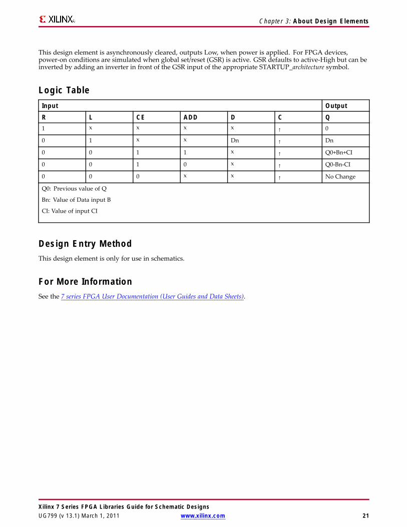
This design element is asynchronously cleared, outputs Low, when power is applied. For FPGA devices,power-on conditions are simulated when global set/reset (GSR) is active. GSR defaults to active-High but can beinverted by adding an inverter in front of the GSR input of the appropriate STARTUP_architecture symbol.
Logic TableInput Output
R L CE ADD D C Q1 x x x x ↑ 0
0 1 x x Dn ↑ Dn
0 0 1 1 x ↑ Q0+Bn+CI
0 0 1 0 x ↑ Q0-Bn-CI
0 0 0 x x ↑ No Change
Q0: Previous value of Q
Bn: Value of Data input B
CI: Value of input CI
Design Entry MethodThis design element is only for use in schematics.
For More InformationSee the 7 series FPGA User Documentation (User Guides and Data Sheets).
Xilinx 7 Series FPGA Libraries Guide for Schematic DesignsUG799 (v 13.1) March 1, 2011 www.xilinx.com 21

Chapter 3: About Design Elements
ACC4Macro: 4-Bit Loadable Cascadable Accumulator with Carry-In, Carry-Out, andSynchronous Reset
IntroductionThis design element can add or subtract a 4-bit unsigned-binary, respectively or two’s-complement word to orfrom the contents of a 4-bit data register and store the results in the register. The register can be loaded with the4-bit word.
When the load input (L) is High, CE is ignored and the data on the D inputs is loaded into the register during theLow-to-High clock (C) transition. ACC4 loads the data on inputs D3 : D0 into the 4-bit register.
This design element operates on either 4-bit unsigned binary numbers or 4-bit two’s-complement numbers. Ifthe inputs are interpreted as unsigned binary, the result can be interpreted as unsigned binary. If the inputsare interpreted as two’s complement, the output can be interpreted as two’s complement. The only functionaldifference between an unsigned binary operation and a two’s-complement operation is how they determinewhen “overflow” occurs. Unsigned binary uses carry-out (CO), while two’s complement uses OFL to determinewhen “overflow” occurs.• For unsigned binary operation, ACC4 can represent numbers between 0 and 15, inclusive. In add mode,
CO is active (High) when the sum exceeds the bounds of the adder/subtracter. In subtract mode, CO is anactive-Low borrow-out and goes Low when the difference exceeds the bounds. The carry-out (CO) isnot registered synchronously with the data outputs. CO always reflects the accumulation of the B inputs(B3 : B0 for ACC4). This allows the cascading of ACC4s by connecting CO of one stage to CI of the nextstage. An unsigned binary “overflow” that is always active-High can be generated by gating the ADDsignal and CO as follows:unsigned overflow = CO XOR ADD
Ignore OFL in unsigned binary operation.• For two’s-complement operation, ACC4 represents numbers between -8 and +7, inclusive. If an addition
or subtraction operation result exceeds this range, the OFL output goes High. The overflow (OFL) is notregistered synchronously with the data outputs. OFL always reflects the accumulation of the B inputs (B3 :B0 for ACC4) and the contents of the register, which allows cascading of ACC4s by connecting OFL of onestage to CI of the next stage.Ignore CO in two’s-complement operation.
Xilinx 7 Series FPGA Libraries Guide for Schematic Designs22 www.xilinx.com UG799 (v 13.1) March 1, 2011

Chapter 3: About Design Elements
The synchronous reset (R) has priority over all other inputs, and when set to High, causes all outputs to go tologic level zero during the Low-to-High clock (C) transition. Clock (C) transitions are ignored when clockenable (CE) is Low.
This design element is asynchronously cleared, outputs Low, when power is applied. For FPGA devices,power-on conditions are simulated when global set/reset (GSR) is active. GSR defaults to active-High but can beinverted by adding an inverter in front of the GSR input of the appropriate STARTUP_architecture symbol.
Logic TableInput Output
R L CE ADD D C Q1 x x x x ↑ 0
0 1 x x Dn ↑ Dn
0 0 1 1 x ↑ Q0+Bn+CI
0 0 1 0 x ↑ Q0-Bn-CI
0 0 0 x x ↑ No Change
Q0: Previous value of Q
Bn: Value of Data input B
CI: Value of input CI
Design Entry MethodThis design element is only for use in schematics.
For More InformationSee the 7 series FPGA User Documentation (User Guides and Data Sheets).
Xilinx 7 Series FPGA Libraries Guide for Schematic DesignsUG799 (v 13.1) March 1, 2011 www.xilinx.com 23

Chapter 3: About Design Elements
ACC8Macro: 8-Bit Loadable Cascadable Accumulator with Carry-In, Carry-Out, andSynchronous Reset
IntroductionThis design element can add or subtract a 8-bit unsigned-binary, respectively or two’s-complement word to orfrom the contents of a 8-bit data register and store the results in the register. The register can be loaded with the8-bit word.
When the load input (L) is High, CE is ignored and the data on the D inputs is loaded into the register during theLow-to-High clock (C) transition. ACC8 loads the data on inputs D7 : D0 into the 8-bit register.
This design element operates on either 8-bit unsigned binary numbers or 8-bit two’s-complement numbers. Ifthe inputs are interpreted as unsigned binary, the result can be interpreted as unsigned binary. If the inputsare interpreted as two’s complement, the output can be interpreted as two’s complement. The only functionaldifference between an unsigned binary operation and a two’s-complement operation is how they determinewhen “overflow” occurs. Unsigned binary uses carry-out (CO), while two’s complement uses OFL to determinewhen “overflow” occurs.
• For unsigned binary operation, ACC8 can represent numbers between 0 and 255, inclusive. In add mode,CO is active (High) when the sum exceeds the bounds of the adder/subtracter. In subtract mode, CO is anactive-Low borrow-out and goes Low when the difference exceeds the bounds. The carry-out (CO) isnot registered synchronously with the data outputs. CO always reflects the accumulation of the B inputs(B3 : B0 for ACC4). This allows the cascading of ACC8s by connecting CO of one stage to CI of the nextstage. An unsigned binary “overflow” that is always active-High can be generated by gating the ADDsignal and CO as follows:
unsigned overflow = CO XOR ADD
Ignore OFL in unsigned binary operation.
• For two’s-complement operation, ACC8 represents numbers between -128 and +127, inclusive. If an additionor subtraction operation result exceeds this range, the OFL output goes High. The overflow (OFL) is notregistered synchronously with the data outputs. OFL always reflects the accumulation of the B inputs (B3 :B0 for ACC8) and the contents of the register, which allows cascading of ACC8s by connecting OFL of onestage to CI of the next stage.
Ignore CO in two’s-complement operation.
The synchronous reset (R) has priority over all other inputs, and when set to High, causes all outputs to go tologic level zero during the Low-to-High clock (C) transition. Clock (C) transitions are ignored when clockenable (CE) is Low.
Xilinx 7 Series FPGA Libraries Guide for Schematic Designs24 www.xilinx.com UG799 (v 13.1) March 1, 2011

Chapter 3: About Design Elements
This design element is asynchronously cleared, outputs Low, when power is applied. For FPGA devices,power-on conditions are simulated when global set/reset (GSR) is active. GSR defaults to active-High but can beinverted by adding an inverter in front of the GSR input of the appropriate STARTUP_architecture symbol.
Logic TableInput Output
R L CE ADD D C Q1 x x x x ↑ 0
0 1 x x Dn ↑ Dn
0 0 1 1 x ↑ Q0+Bn+CI
0 0 1 0 x ↑ Q0-Bn-CI
0 0 0 x x ↑ No Change
Q0: Previous value of Q
Bn: Value of Data input B
CI: Value of input CI
Design Entry MethodThis design element is only for use in schematics.
For More InformationSee the 7 series FPGA User Documentation (User Guides and Data Sheets).
Xilinx 7 Series FPGA Libraries Guide for Schematic DesignsUG799 (v 13.1) March 1, 2011 www.xilinx.com 25

Chapter 3: About Design Elements
ADD16Macro: 16-Bit Cascadable Full Adder with Carry-In, Carry-Out, and Overflow
IntroductionThis design element adds two words and a carry-in (CI), producing a sum output and carry-out (CO) or overflow(OFL). The factors added are A15:A0, B15:B0 and CI, producing the sum output S15:S0 and CO (or OFL).
Logic TableInput Output
A B SAn Bn An+Bn+CI
CI: Value of input CI.
Unsigned Binary Versus Two’s Complement -This design element can operate on either 16-bit unsigned binarynumbers or 16-bit two’s-complement numbers, respectively. If the inputs are interpreted as unsigned binary, theresult can be interpreted as unsigned binary. If the inputs are interpreted as two’s complement, the output can beinterpreted as two’s complement. The only functional difference between an unsigned binary operation and atwo’s-complement operation is the way they determine when “overflow” occurs. Unsigned binary uses CO,while two’s-complement uses OFL to determine when “overflow” occurs. To interpret the inputs as unsignedbinary, follow the CO output. To interpret the inputs as two’s complement, follow the OFL output.
Unsigned Binary Operation -For unsigned binary operation, this element represents numbers between 0 and65535, inclusive. OFL is ignored in unsigned binary operation.
Two’s-Complement Operation -For two’s-complement operation, this element can represent numbers between-32768 and +32767, inclusive. OFL is active (High) when the sum exceeds the bounds of the adder. CO is ignoredin two’s-complement operation.
Design Entry MethodThis design element is only for use in schematics.
For More InformationSee the 7 series FPGA User Documentation (User Guides and Data Sheets).
Xilinx 7 Series FPGA Libraries Guide for Schematic Designs26 www.xilinx.com UG799 (v 13.1) March 1, 2011

Chapter 3: About Design Elements
ADD4Macro: 4-Bit Cascadable Full Adder with Carry-In, Carry-Out, and Overflow
IntroductionThis design element adds two words and a carry-in (CI), producing a sum output and carry-out (CO) or overflow(OFL). The factors added are A3:A0, B3:B0, and CI producing the sum output S3:S0 and CO (or OFL).
Logic TableInput Output
A B SAn Bn An+Bn+CI
CI: Value of input CI.
Unsigned Binary Versus Two’s Complement -This design element can operate on either 4-bit unsigned binarynumbers or 4-bit two’s-complement numbers, respectively. If the inputs are interpreted as unsigned binary, theresult can be interpreted as unsigned binary. If the inputs are interpreted as two’s complement, the output can beinterpreted as two’s complement. The only functional difference between an unsigned binary operation and atwo’s-complement operation is the way they determine when “overflow” occurs. Unsigned binary uses CO,while two’s-complement uses OFL to determine when “overflow” occurs. To interpret the inputs as unsignedbinary, follow the CO output. To interpret the inputs as two’s complement, follow the OFL output.
Unsigned Binary Operation -For unsigned binary operation, this element represents numbers from 0 to 15,inclusive. OFL is ignored in unsigned binary operation.
Two’s-Complement Operation -For two’s-complement operation, this element can represent numbers between-8 and +7, inclusive. OFL is active (High) when the sum exceeds the bounds of the adder. CO is ignored intwo’s-complement operation.
Design Entry MethodThis design element is only for use in schematics.
For More InformationSee the 7 series FPGA User Documentation (User Guides and Data Sheets).
Xilinx 7 Series FPGA Libraries Guide for Schematic DesignsUG799 (v 13.1) March 1, 2011 www.xilinx.com 27

Chapter 3: About Design Elements
ADD8Macro: 8-Bit Cascadable Full Adder with Carry-In, Carry-Out, and Overflow
IntroductionThis design element adds two words and a carry-in (CI), producing a sum output and carry-out (CO) or overflow(OFL). The factors added are A7:A0, B7:B0, and CI, producing the sum output S7:S0 and CO (or OFL).
Logic TableInput Output
A B SAn Bn An+Bn+CI
CI: Value of input CI.
Unsigned Binary Versus Two’s Complement -This design element can operate on either 8-bit unsigned binarynumbers or 8-bit two’s-complement numbers, respectively. If the inputs are interpreted as unsigned binary, theresult can be interpreted as unsigned binary. If the inputs are interpreted as two’s complement, the output can beinterpreted as two’s complement. The only functional difference between an unsigned binary operation and atwo’s-complement operation is the way they determine when “overflow” occurs. Unsigned binary uses CO,while two’s-complement uses OFL to determine when “overflow” occurs. To interpret the inputs as unsignedbinary, follow the CO output. To interpret the inputs as two’s complement, follow the OFL output.
Unsigned Binary Operation -For unsigned binary operation, this element represents numbers between 0 and255, inclusive. OFL is ignored in unsigned binary operation.
Two’s-Complement Operation -For two’s-complement operation, this element can represent numbers between-128 and +127, inclusive. OFL is active (High) when the sum exceeds the bounds of the adder. CO is ignored intwo’s-complement operation.
Design Entry MethodThis design element is only for use in schematics.
For More InformationSee the 7 series FPGA User Documentation (User Guides and Data Sheets).
Xilinx 7 Series FPGA Libraries Guide for Schematic Designs28 www.xilinx.com UG799 (v 13.1) March 1, 2011

Chapter 3: About Design Elements
ADSU16Macro: 16-Bit Cascadable Adder/Subtracter with Carry-In, Carry-Out, and Overflow
IntroductionWhen the ADD input is High, this element adds two 16-bit words (A15:A0 and B15:B0) and a carry-in (CI),producing a 16-bit sum output (S15:S0) and carry-out (CO) or overflow (OFL).
When the ADD input is Low, this element subtracts B15:B0 from A15:A0, producing a difference output anda carry-out (CO) or an overflow (OFL).
In add mode, CO and CI are active-High. In subtract mode, CO and CI are active-Low. OFL is active-High inadd and subtract modes.
Logic TableInput Output
ADD A B S1 An Bn An+Bn+CI*
0 An Bn An-Bn-CI*
CI*: ADD = 0, CI, CO active LOW
CI*: ADD = 1, CI, CO active HIGH
Unsigned Binary Versus Two’s Complement -This design element can operate on either 16-bit unsigned binarynumbers or 16-bit two’s-complement numbers. If the inputs are interpreted as unsigned binary, the resultcan be interpreted as unsigned binary. If the inputs are interpreted as two’s complement, the output can beinterpreted as two’s complement. The only functional difference between an unsigned binary operation and atwo’s-complement operation is the way they determine when “overflow” occurs. Unsigned binary uses CO,while two’s complement uses OFL to determine when “overflow” occurs.
With adder/subtracters, either unsigned binary or two’s-complement operations cause an overflow. If theresult crosses the overflow boundary, an overflow is generated. Similarly, when the result crosses the carry-outboundary, a carry-out is generated.
Unsigned Binary Operation -For unsigned binary operation, this element can represent numbers between 0 and65535, inclusive. In add mode, CO is active (High) when the sum exceeds the bounds of the adder/subtracter. Insubtract mode, CO is an active-Low borrow-out and goes Low when the difference exceeds the bounds.
An unsigned binary “overflow” that is always active-High can be generated by gating the ADD signal and COas follows:
unsigned overflow = CO XOR ADD
OFL is ignored in unsigned binary operation.
Xilinx 7 Series FPGA Libraries Guide for Schematic DesignsUG799 (v 13.1) March 1, 2011 www.xilinx.com 29

Chapter 3: About Design Elements
Two’s-Complement Operation -For two’s-complement operation, this element can represent numbers between-32768 and +32767, inclusive.
If an addition or subtraction operation result exceeds this range, the OFL output goes High. CO is ignored intwo’s-complement operation.
Design Entry MethodThis design element is only for use in schematics.
For More InformationSee the 7 series FPGA User Documentation (User Guides and Data Sheets).
Xilinx 7 Series FPGA Libraries Guide for Schematic Designs30 www.xilinx.com UG799 (v 13.1) March 1, 2011
Chapter 3: About Design Elements
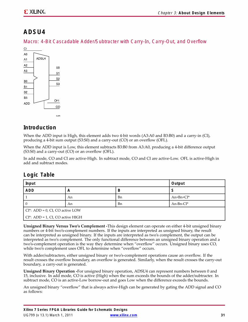
ADSU4Macro: 4-Bit Cascadable Adder/Subtracter with Carry-In, Carry-Out, and Overflow
IntroductionWhen the ADD input is High, this element adds two 4-bit words (A3:A0 and B3:B0) and a carry-in (CI),producing a 4-bit sum output (S3:S0) and a carry-out (CO) or an overflow (OFL).
When the ADD input is Low, this element subtracts B3:B0 from A3:A0, producing a 4-bit difference output(S3:S0) and a carry-out (CO) or an overflow (OFL).
In add mode, CO and CI are active-High. In subtract mode, CO and CI are active-Low. OFL is active-High inadd and subtract modes.
Logic TableInput Output
ADD A B S1 An Bn An+Bn+CI*
0 An Bn An-Bn-CI*
CI*: ADD = 0, CI, CO active LOW
CI*: ADD = 1, CI, CO active HIGH
Unsigned Binary Versus Two’s Complement -This design element can operate on either 4-bit unsigned binarynumbers or 4-bit two’s-complement numbers. If the inputs are interpreted as unsigned binary, the resultcan be interpreted as unsigned binary. If the inputs are interpreted as two’s complement, the output can beinterpreted as two’s complement. The only functional difference between an unsigned binary operation and atwo’s-complement operation is the way they determine when “overflow” occurs. Unsigned binary uses CO,while two’s complement uses OFL to determine when “overflow” occurs.
With adder/subtracters, either unsigned binary or two’s-complement operations cause an overflow. If theresult crosses the overflow boundary, an overflow is generated. Similarly, when the result crosses the carry-outboundary, a carry-out is generated.
Unsigned Binary Operation -For unsigned binary operation, ADSU4 can represent numbers between 0 and15, inclusive. In add mode, CO is active (High) when the sum exceeds the bounds of the adder/subtracter. Insubtract mode, CO is an active-Low borrow-out and goes Low when the difference exceeds the bounds.
An unsigned binary “overflow” that is always active-High can be generated by gating the ADD signal and COas follows:
Xilinx 7 Series FPGA Libraries Guide for Schematic DesignsUG799 (v 13.1) March 1, 2011 www.xilinx.com 31

Chapter 3: About Design Elements
unsigned overflow = CO XOR ADD
OFL is ignored in unsigned binary operation.
Two’s-Complement Operation -For two’s-complement operation, this element can represent numbers between-8 and +7, inclusive.
If an addition or subtraction operation result exceeds this range, the OFL output goes High. CO is ignored intwo’s-complement operation.
Design Entry MethodThis design element is only for use in schematics.
For More InformationSee the 7 series FPGA User Documentation (User Guides and Data Sheets).
Xilinx 7 Series FPGA Libraries Guide for Schematic Designs32 www.xilinx.com UG799 (v 13.1) March 1, 2011
Chapter 3: About Design Elements
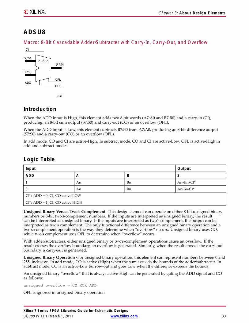
ADSU8Macro: 8-Bit Cascadable Adder/Subtracter with Carry-In, Carry-Out, and Overflow
IntroductionWhen the ADD input is High, this element adds two 8-bit words (A7:A0 and B7:B0) and a carry-in (CI),producing, an 8-bit sum output (S7:S0) and carry-out (CO) or an overflow (OFL).
When the ADD input is Low, this element subtracts B7:B0 from A7:A0, producing an 8-bit difference output(S7:S0) and a carry-out (CO) or an overflow (OFL).
In add mode, CO and CI are active-High. In subtract mode, CO and CI are active-Low. OFL is active-High inadd and subtract modes.
Logic TableInput Output
ADD A B S1 An Bn An+Bn+CI*
0 An Bn An-Bn-CI*
CI*: ADD = 0, CI, CO active LOW
CI*: ADD = 1, CI, CO active HIGH
Unsigned Binary Versus Two’s Complement -This design element can operate on either 8-bit unsigned binarynumbers or 8-bit two’s-complement numbers. If the inputs are interpreted as unsigned binary, the resultcan be interpreted as unsigned binary. If the inputs are interpreted as two’s complement, the output can beinterpreted as two’s complement. The only functional difference between an unsigned binary operation and atwo’s-complement operation is the way they determine when “overflow” occurs. Unsigned binary uses CO,while two’s complement uses OFL to determine when “overflow” occurs.
With adder/subtracters, either unsigned binary or two’s-complement operations cause an overflow. If theresult crosses the overflow boundary, an overflow is generated. Similarly, when the result crosses the carry-outboundary, a carry-out is generated.
Unsigned Binary Operation -For unsigned binary operation, this element can represent numbers between 0 and255, inclusive. In add mode, CO is active (High) when the sum exceeds the bounds of the adder/subtracter. Insubtract mode, CO is an active-Low borrow-out and goes Low when the difference exceeds the bounds.
An unsigned binary “overflow” that is always active-High can be generated by gating the ADD signal and COas follows:
unsigned overflow = CO XOR ADD
OFL is ignored in unsigned binary operation.
Xilinx 7 Series FPGA Libraries Guide for Schematic DesignsUG799 (v 13.1) March 1, 2011 www.xilinx.com 33
Chapter 3: About Design Elements
Two’s-Complement Operation -For two’s-complement operation, this element can represent numbers between-128 and +127, inclusive.
If an addition or subtraction operation result exceeds this range, the OFL output goes High. CO is ignored intwo’s-complement operation.
Design Entry MethodThis design element is only for use in schematics.
For More InformationSee the 7 series FPGA User Documentation (User Guides and Data Sheets).
Xilinx 7 Series FPGA Libraries Guide for Schematic Designs34 www.xilinx.com UG799 (v 13.1) March 1, 2011

Chapter 3: About Design Elements
AND12Macro: 12- Input AND Gate with Non-Inverted Inputs
IntroductionAND functions of up to five inputs are available in any combination of inverting and non-inverting inputs. ANDfunctions of six to nine inputs, 12 inputs, and 16 inputs are available with noninverting inputs. To make someor all inputs inverting, use external inverters. Because each input uses a CLB resource, replace functions withunused inputs with functions having the appropriate number of inputs.
Design Entry MethodThis design element is only for use in schematics.
For More InformationSee the 7 series FPGA User Documentation (User Guides and Data Sheets).
Xilinx 7 Series FPGA Libraries Guide for Schematic DesignsUG799 (v 13.1) March 1, 2011 www.xilinx.com 35

Chapter 3: About Design Elements
AND1616- Input AND Gate with Non-Inverted Inputs
IntroductionAND functions of up to five inputs are available in any combination of inverting and non-inverting inputs. ANDfunctions of six to nine inputs, 12 inputs, and 16 inputs are available with noninverting inputs. To make someor all inputs inverting, use external inverters. Because each input uses a CLB resource, replace functions withunused inputs with functions having the appropriate number of inputs.
Design Entry MethodThis design element is only for use in schematics.
For More InformationSee the 7 series FPGA User Documentation (User Guides and Data Sheets).
Xilinx 7 Series FPGA Libraries Guide for Schematic Designs36 www.xilinx.com UG799 (v 13.1) March 1, 2011

Chapter 3: About Design Elements
AND2Primitive: 2-Input AND Gate with Non-Inverted Inputs
IntroductionAND functions of up to five inputs are available in any combination of inverting and non-inverting inputs. ANDfunctions of six to nine inputs, 12 inputs, and 16 inputs are available with noninverting inputs. To make someor all inputs inverting, use external inverters. Because each input uses a CLB resource, replace functions withunused inputs with functions having the appropriate number of inputs.
Design Entry MethodThis design element is only for use in schematics.
For More InformationSee the 7 series FPGA User Documentation (User Guides and Data Sheets).
Xilinx 7 Series FPGA Libraries Guide for Schematic DesignsUG799 (v 13.1) March 1, 2011 www.xilinx.com 37

Chapter 3: About Design Elements
AND2B1Primitive: 2-Input AND Gate with 1 Inverted and 1 Non-Inverted Inputs
IntroductionAND functions of up to five inputs are available in any combination of inverting and non-inverting inputs. ANDfunctions of six to nine inputs, 12 inputs, and 16 inputs are available with noninverting inputs. To make someor all inputs inverting, use external inverters. Because each input uses a CLB resource, replace functions withunused inputs with functions having the appropriate number of inputs.
Design Entry MethodThis design element is only for use in schematics.
For More InformationSee the 7 series FPGA User Documentation (User Guides and Data Sheets).
Xilinx 7 Series FPGA Libraries Guide for Schematic Designs38 www.xilinx.com UG799 (v 13.1) March 1, 2011

Chapter 3: About Design Elements
AND2B1LPrimitive: Two input AND gate implemented in place of a Slice Latch
IntroductionThis element allows the specification of a configurable Slice latch to take the function of a two input ANDgate with one input inverted (see Logic Table). The use of this element can reduce logic levels and increaselogic density of the part by trading off register/latch resources for logic. Xilinx suggests caution when usingthis component as it can affect register packing and density since specifying one or more AND2B1L or OR2Lcomponents in a Slice disallows the use of the remaining registers and latches.
Logic TableInputs Outputs
DI SRI O0 0 0
0 1 0
1 0 1
1 1 0
Port DescriptionsPort Type Width FunctionO Output 1 Output of the AND gate.
DI Input 1 Active high input that is generally connected to sourcing LUT locatedin the same Slice.
SRI Input 1 Active low input that is generally source from outside of the Slice.
Note To allow more than one AND2B1L or OR2B1L to be packed intoa single Slice, a common signal must be connected to this input.
Design Entry MethodThis design element can be used in schematics.
For More Information• See the 7 series FPGA SelectIO Resources User Guide.
• See the 7 series FPGA User Documentation (User Guides and Data Sheets).
Xilinx 7 Series FPGA Libraries Guide for Schematic DesignsUG799 (v 13.1) March 1, 2011 www.xilinx.com 39

Chapter 3: About Design Elements
AND2B2Primitive: 2-Input AND Gate with Inverted Inputs
IntroductionAND functions of up to five inputs are available in any combination of inverting and non-inverting inputs. ANDfunctions of six to nine inputs, 12 inputs, and 16 inputs are available with noninverting inputs. To make someor all inputs inverting, use external inverters. Because each input uses a CLB resource, replace functions withunused inputs with functions having the appropriate number of inputs.
Design Entry MethodThis design element is only for use in schematics.
For More InformationSee the 7 series FPGA User Documentation (User Guides and Data Sheets).
Xilinx 7 Series FPGA Libraries Guide for Schematic Designs40 www.xilinx.com UG799 (v 13.1) March 1, 2011

Chapter 3: About Design Elements
AND3Primitive: 3-Input AND Gate with Non-Inverted Inputs
IntroductionAND functions of up to five inputs are available in any combination of inverting and non-inverting inputs. ANDfunctions of six to nine inputs, 12 inputs, and 16 inputs are available with noninverting inputs. To make someor all inputs inverting, use external inverters. Because each input uses a CLB resource, replace functions withunused inputs with functions having the appropriate number of inputs.
Design Entry MethodThis design element is only for use in schematics.
For More InformationSee the 7 series FPGA User Documentation (User Guides and Data Sheets).
Xilinx 7 Series FPGA Libraries Guide for Schematic DesignsUG799 (v 13.1) March 1, 2011 www.xilinx.com 41

Chapter 3: About Design Elements
AND3B1Primitive: 3-Input AND Gate with 1 Inverted and 2 Non-Inverted Inputs
IntroductionAND functions of up to five inputs are available in any combination of inverting and non-inverting inputs. ANDfunctions of six to nine inputs, 12 inputs, and 16 inputs are available with noninverting inputs. To make someor all inputs inverting, use external inverters. Because each input uses a CLB resource, replace functions withunused inputs with functions having the appropriate number of inputs.
Design Entry MethodThis design element is only for use in schematics.
For More InformationSee the 7 series FPGA User Documentation (User Guides and Data Sheets).
Xilinx 7 Series FPGA Libraries Guide for Schematic Designs42 www.xilinx.com UG799 (v 13.1) March 1, 2011

Chapter 3: About Design Elements
AND3B2Primitive: 3-Input AND Gate with 2 Inverted and 1 Non-Inverted Inputs
IntroductionAND functions of up to five inputs are available in any combination of inverting and non-inverting inputs. ANDfunctions of six to nine inputs, 12 inputs, and 16 inputs are available with noninverting inputs. To make someor all inputs inverting, use external inverters. Because each input uses a CLB resource, replace functions withunused inputs with functions having the appropriate number of inputs.
Design Entry MethodThis design element is only for use in schematics.
For More InformationSee the 7 series FPGA User Documentation (User Guides and Data Sheets).
Xilinx 7 Series FPGA Libraries Guide for Schematic DesignsUG799 (v 13.1) March 1, 2011 www.xilinx.com 43

Chapter 3: About Design Elements
AND3B3Primitive: 3-Input AND Gate with Inverted Inputs
IntroductionAND functions of up to five inputs are available in any combination of inverting and non-inverting inputs. ANDfunctions of six to nine inputs, 12 inputs, and 16 inputs are available with noninverting inputs. To make someor all inputs inverting, use external inverters. Because each input uses a CLB resource, replace functions withunused inputs with functions having the appropriate number of inputs.
Design Entry MethodThis design element is only for use in schematics.
For More InformationSee the 7 series FPGA User Documentation (User Guides and Data Sheets).
Xilinx 7 Series FPGA Libraries Guide for Schematic Designs44 www.xilinx.com UG799 (v 13.1) March 1, 2011

Chapter 3: About Design Elements
AND4Primitive: 4-Input AND Gate with Non-Inverted Inputs
IntroductionAND functions of up to five inputs are available in any combination of inverting and non-inverting inputs. ANDfunctions of six to nine inputs, 12 inputs, and 16 inputs are available with noninverting inputs. To make someor all inputs inverting, use external inverters. Because each input uses a CLB resource, replace functions withunused inputs with functions having the appropriate number of inputs.
Design Entry MethodThis design element is only for use in schematics.
For More InformationSee the 7 series FPGA User Documentation (User Guides and Data Sheets).
Xilinx 7 Series FPGA Libraries Guide for Schematic DesignsUG799 (v 13.1) March 1, 2011 www.xilinx.com 45

Chapter 3: About Design Elements
AND4B1Primitive: 4-Input AND Gate with 1 Inverted and 3 Non-Inverted Inputs
IntroductionAND functions of up to five inputs are available in any combination of inverting and non-inverting inputs. ANDfunctions of six to nine inputs, 12 inputs, and 16 inputs are available with noninverting inputs. To make someor all inputs inverting, use external inverters. Because each input uses a CLB resource, replace functions withunused inputs with functions having the appropriate number of inputs.
Design Entry MethodThis design element is only for use in schematics.
For More InformationSee the 7 series FPGA User Documentation (User Guides and Data Sheets).
Xilinx 7 Series FPGA Libraries Guide for Schematic Designs46 www.xilinx.com UG799 (v 13.1) March 1, 2011

Chapter 3: About Design Elements
AND4B2Primitive: 4-Input AND Gate with 2 Inverted and 2 Non-Inverted Inputs
IntroductionAND functions of up to five inputs are available in any combination of inverting and non-inverting inputs. ANDfunctions of six to nine inputs, 12 inputs, and 16 inputs are available with noninverting inputs. To make someor all inputs inverting, use external inverters. Because each input uses a CLB resource, replace functions withunused inputs with functions having the appropriate number of inputs.
Design Entry MethodThis design element is only for use in schematics.
For More InformationSee the 7 series FPGA User Documentation (User Guides and Data Sheets).
Xilinx 7 Series FPGA Libraries Guide for Schematic DesignsUG799 (v 13.1) March 1, 2011 www.xilinx.com 47
Chapter 3: About Design Elements
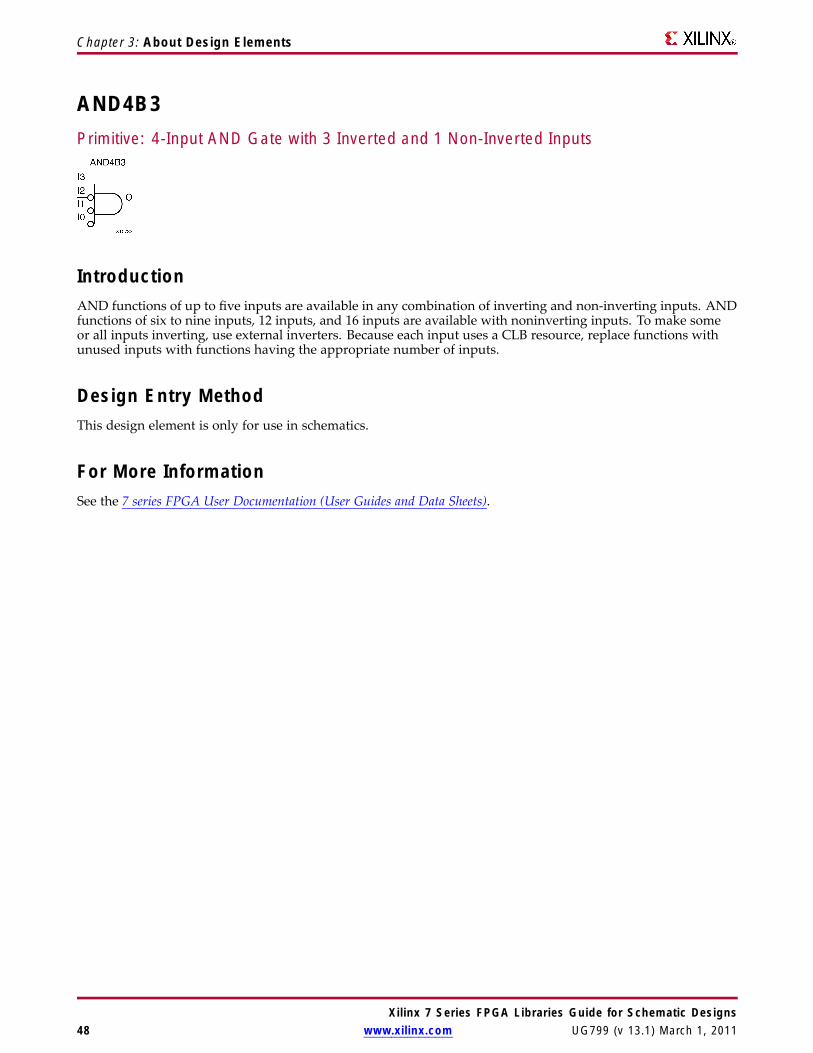
AND4B3Primitive: 4-Input AND Gate with 3 Inverted and 1 Non-Inverted Inputs
IntroductionAND functions of up to five inputs are available in any combination of inverting and non-inverting inputs. ANDfunctions of six to nine inputs, 12 inputs, and 16 inputs are available with noninverting inputs. To make someor all inputs inverting, use external inverters. Because each input uses a CLB resource, replace functions withunused inputs with functions having the appropriate number of inputs.
Design Entry MethodThis design element is only for use in schematics.
For More InformationSee the 7 series FPGA User Documentation (User Guides and Data Sheets).
Xilinx 7 Series FPGA Libraries Guide for Schematic Designs48 www.xilinx.com UG799 (v 13.1) March 1, 2011

Chapter 3: About Design Elements
AND4B4Primitive: 4-Input AND Gate with Inverted Inputs
IntroductionAND functions of up to five inputs are available in any combination of inverting and non-inverting inputs. ANDfunctions of six to nine inputs, 12 inputs, and 16 inputs are available with noninverting inputs. To make someor all inputs inverting, use external inverters. Because each input uses a CLB resource, replace functions withunused inputs with functions having the appropriate number of inputs.
Design Entry MethodThis design element is only for use in schematics.
For More InformationSee the 7 series FPGA User Documentation (User Guides and Data Sheets).
Xilinx 7 Series FPGA Libraries Guide for Schematic DesignsUG799 (v 13.1) March 1, 2011 www.xilinx.com 49
Chapter 3: About Design Elements
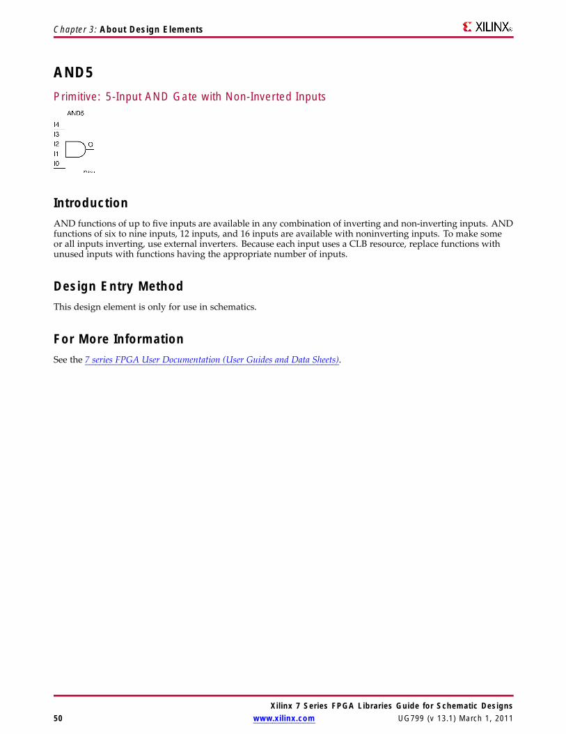
AND5Primitive: 5-Input AND Gate with Non-Inverted Inputs
IntroductionAND functions of up to five inputs are available in any combination of inverting and non-inverting inputs. ANDfunctions of six to nine inputs, 12 inputs, and 16 inputs are available with noninverting inputs. To make someor all inputs inverting, use external inverters. Because each input uses a CLB resource, replace functions withunused inputs with functions having the appropriate number of inputs.
Design Entry MethodThis design element is only for use in schematics.
For More InformationSee the 7 series FPGA User Documentation (User Guides and Data Sheets).
Xilinx 7 Series FPGA Libraries Guide for Schematic Designs50 www.xilinx.com UG799 (v 13.1) March 1, 2011

Chapter 3: About Design Elements
AND5B1Primitive: 5-Input AND Gate with 1 Inverted and 4 Non-Inverted Inputs
IntroductionAND functions of up to five inputs are available in any combination of inverting and non-inverting inputs. ANDfunctions of six to nine inputs, 12 inputs, and 16 inputs are available with noninverting inputs. To make someor all inputs inverting, use external inverters. Because each input uses a CLB resource, replace functions withunused inputs with functions having the appropriate number of inputs.
Design Entry MethodThis design element is only for use in schematics.
For More InformationSee the 7 series FPGA User Documentation (User Guides and Data Sheets).
Xilinx 7 Series FPGA Libraries Guide for Schematic DesignsUG799 (v 13.1) March 1, 2011 www.xilinx.com 51

Chapter 3: About Design Elements
AND5B2Primitive: 5-Input AND Gate with 2 Inverted and 3 Non-Inverted Inputs
IntroductionAND functions of up to five inputs are available in any combination of inverting and non-inverting inputs. ANDfunctions of six to nine inputs, 12 inputs, and 16 inputs are available with noninverting inputs. To make someor all inputs inverting, use external inverters. Because each input uses a CLB resource, replace functions withunused inputs with functions having the appropriate number of inputs.
Design Entry MethodThis design element is only for use in schematics.
For More InformationSee the 7 series FPGA User Documentation (User Guides and Data Sheets).
Xilinx 7 Series FPGA Libraries Guide for Schematic Designs52 www.xilinx.com UG799 (v 13.1) March 1, 2011

Chapter 3: About Design Elements
AND5B3Primitive: 5-Input AND Gate with 3 Inverted and 2 Non-Inverted Inputs
IntroductionAND functions of up to five inputs are available in any combination of inverting and non-inverting inputs. ANDfunctions of six to nine inputs, 12 inputs, and 16 inputs are available with noninverting inputs. To make someor all inputs inverting, use external inverters. Because each input uses a CLB resource, replace functions withunused inputs with functions having the appropriate number of inputs.
Design Entry MethodThis design element is only for use in schematics.
For More InformationSee the 7 series FPGA User Documentation (User Guides and Data Sheets).
Xilinx 7 Series FPGA Libraries Guide for Schematic DesignsUG799 (v 13.1) March 1, 2011 www.xilinx.com 53
Chapter 3: About Design Elements
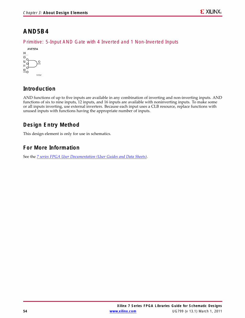
AND5B4Primitive: 5-Input AND Gate with 4 Inverted and 1 Non-Inverted Inputs
IntroductionAND functions of up to five inputs are available in any combination of inverting and non-inverting inputs. ANDfunctions of six to nine inputs, 12 inputs, and 16 inputs are available with noninverting inputs. To make someor all inputs inverting, use external inverters. Because each input uses a CLB resource, replace functions withunused inputs with functions having the appropriate number of inputs.
Design Entry MethodThis design element is only for use in schematics.
For More InformationSee the 7 series FPGA User Documentation (User Guides and Data Sheets).
Xilinx 7 Series FPGA Libraries Guide for Schematic Designs54 www.xilinx.com UG799 (v 13.1) March 1, 2011

Chapter 3: About Design Elements
AND5B5Primitive: 5-Input AND Gate with Inverted Inputs
IntroductionAND functions of up to five inputs are available in any combination of inverting and non-inverting inputs. ANDfunctions of six to nine inputs, 12 inputs, and 16 inputs are available with noninverting inputs. To make someor all inputs inverting, use external inverters. Because each input uses a CLB resource, replace functions withunused inputs with functions having the appropriate number of inputs.
Design Entry MethodThis design element is only for use in schematics.
For More InformationSee the 7 series FPGA User Documentation (User Guides and Data Sheets).
Xilinx 7 Series FPGA Libraries Guide for Schematic DesignsUG799 (v 13.1) March 1, 2011 www.xilinx.com 55

Chapter 3: About Design Elements
AND6Macro: 6-Input AND Gate with Non-Inverted Inputs
IntroductionAND functions of up to five inputs are available in any combination of inverting and non-inverting inputs. ANDfunctions of six to nine inputs, 12 inputs, and 16 inputs are available with noninverting inputs. To make someor all inputs inverting, use external inverters. Because each input uses a CLB resource, replace functions withunused inputs with functions having the appropriate number of inputs.
Design Entry MethodThis design element is only for use in schematics.
For More InformationSee the 7 series FPGA User Documentation (User Guides and Data Sheets).
Xilinx 7 Series FPGA Libraries Guide for Schematic Designs56 www.xilinx.com UG799 (v 13.1) March 1, 2011

Chapter 3: About Design Elements
AND7Macro: 7-Input AND Gate with Non-Inverted Inputs
IntroductionAND functions of up to five inputs are available in any combination of inverting and non-inverting inputs. ANDfunctions of six to nine inputs, 12 inputs, and 16 inputs are available with noninverting inputs. To make someor all inputs inverting, use external inverters. Because each input uses a CLB resource, replace functions withunused inputs with functions having the appropriate number of inputs.
Design Entry MethodThis design element is only for use in schematics.
For More InformationSee the 7 series FPGA User Documentation (User Guides and Data Sheets).
Xilinx 7 Series FPGA Libraries Guide for Schematic DesignsUG799 (v 13.1) March 1, 2011 www.xilinx.com 57
Chapter 3: About Design Elements
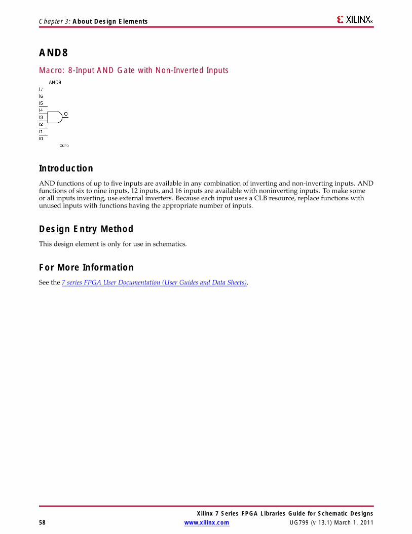
AND8Macro: 8-Input AND Gate with Non-Inverted Inputs
IntroductionAND functions of up to five inputs are available in any combination of inverting and non-inverting inputs. ANDfunctions of six to nine inputs, 12 inputs, and 16 inputs are available with noninverting inputs. To make someor all inputs inverting, use external inverters. Because each input uses a CLB resource, replace functions withunused inputs with functions having the appropriate number of inputs.
Design Entry MethodThis design element is only for use in schematics.
For More InformationSee the 7 series FPGA User Documentation (User Guides and Data Sheets).
Xilinx 7 Series FPGA Libraries Guide for Schematic Designs58 www.xilinx.com UG799 (v 13.1) March 1, 2011

Chapter 3: About Design Elements
AND9Macro: 9-Input AND Gate with Non-Inverted Inputs
IntroductionAND functions of up to five inputs are available in any combination of inverting and non-inverting inputs. ANDfunctions of six to nine inputs, 12 inputs, and 16 inputs are available with noninverting inputs. To make someor all inputs inverting, use external inverters. Because each input uses a CLB resource, replace functions withunused inputs with functions having the appropriate number of inputs.
Design Entry MethodThis design element is only for use in schematics.
For More InformationSee the 7 series FPGA User Documentation (User Guides and Data Sheets).
Xilinx 7 Series FPGA Libraries Guide for Schematic DesignsUG799 (v 13.1) March 1, 2011 www.xilinx.com 59

Chapter 3: About Design Elements
BRLSHFT4Macro: 4-Bit Barrel Shifter
IntroductionThis design element is a 4-bit barrel shifter that can rotate four inputs (I3 : I0) up to four places. The controlinputs (S1 and S0) determine the number of positions, from one to four, that the data is rotated. The four outputs(O3 : O0) reflect the shifted data inputs.
Logic TableInputs Outputs
S1 S0 I0 I1 I2 I3 O0 O1 O2 O30 0 a b c d a b c d
0 1 a b c d b c d a
1 0 a b c d c d a b
1 1 a b c d d a b c
Design Entry MethodThis design element is only for use in schematics.
For More InformationSee the 7 series FPGA User Documentation (User Guides and Data Sheets).
Xilinx 7 Series FPGA Libraries Guide for Schematic Designs60 www.xilinx.com UG799 (v 13.1) March 1, 2011

Chapter 3: About Design Elements
BRLSHFT8Macro: 8-Bit Barrel Shifter
IntroductionThis design element is an 8-bit barrel shifter, can rotate the eight inputs (I7 : I0) up to eight places. The controlinputs (S2 : S0) determine the number of positions, from one to eight, that the data is rotated. The eight outputs(O7 : O0) reflect the shifted data inputs.
Logic TableInputs Outputs
S2 S1 S0 I0 I1 I2 I3 I4 I5 I6 I7 O0 O1 O2 O3 O4 O5 O6 O70 0 0 a b c d e f g h a b c d e f g h
0 0 1 a b c d e f g h b c d e f g h a
0 1 0 a b c d e f g h c d e f g h a b
0 1 1 a b c d e f g h d e f g h a b c
1 0 0 a b c d e f g h e f g h a b c d
1 0 1 a b c d e f g h f g h a b c d e
1 1 0 a b c d e f g h g h a b c d e f
1 1 1 a b c d e f g h h a b c d e f g
Design Entry MethodThis design element is only for use in schematics.
For More InformationSee the 7 series FPGA User Documentation (User Guides and Data Sheets).
Xilinx 7 Series FPGA Libraries Guide for Schematic DesignsUG799 (v 13.1) March 1, 2011 www.xilinx.com 61

Chapter 3: About Design Elements
BSCAN_JTAG_MONE2Primitive: Boundary Scan JTAG Monitor
IntroductionThis design element provides the ability to monitor external JTAG signals. Note that for specific information onboundary scan for an architecture, see the Configuration User Guide for the device.
Port DescriptionsPort Type Width FunctionTCK Output 1 Scan Clock output. Fabric connection to TAP Clock pin.
TDI Output 1 TDI output from TAP controller.
TMS Output 1 Test Mode Select input. Fabric connection to TAP.
Design Entry MethodThis design element can be used in schematics.
For More InformationSee the 7 series FPGA User Documentation (User Guides and Data Sheets).
Xilinx 7 Series FPGA Libraries Guide for Schematic Designs62 www.xilinx.com UG799 (v 13.1) March 1, 2011

Chapter 3: About Design Elements
BSCANE2Primitive: Boundary Scan User Instruction
IntroductionThis design element allows access to and from internal logic by the JTAG Boundary Scan logic controller. Thisallows for communication between the internal running design and the dedicated JTAG pins of the FPGA. Eachinstance of this design element will handle one JTAG USER instruction (USER1 through USER4) as set with theJTAG_CHAIN attribute. To handle all four USER instructions, instantiate four of these elements and set theJTAG_CHAIN attribute appropriately. Note that for specific information on boundary scan for an architecture,see the Configuration User Guide for the device.
Port DescriptionsPort Type Width FunctionCAPTURE Output 1 CAPTURE output from TAP controller.
DRCK Output 1 Gated TCK output. When SEL is asserted, DRCK toggles whenCAPTURE or SHIFT are asserted.
RESET Output 1 Reset output for TAP controller.
RUNTEST Output 1 RUNTEST asserted when TAP controller is in Run-Test/Idle state.
SEL Output 1 USER active output.
SHIFT Output 1 SHIFT output from TAP controller.
TCK Output 1 Scan Clock output. Fabric connection to TAP Clock pin.
TDI Output 1 TDI output from TAP controller.
TDO Input 1 Data input for USER function.
TMS Output 1 Test Mode Select input. Fabric connection to TAP
UPDATE Output 1 UPDATE output from TAP controller
Design Entry MethodThis design element can be used in schematics.
Available AttributesAttribute Type Allowed Values Default DescriptionJTAG_CHAIN DECIMAL 1, 2, 3, 4 1 Value for USER command.
Xilinx 7 Series FPGA Libraries Guide for Schematic DesignsUG799 (v 13.1) March 1, 2011 www.xilinx.com 63

Chapter 3: About Design Elements
For More InformationSee the 7 series FPGA User Documentation (User Guides and Data Sheets).
Xilinx 7 Series FPGA Libraries Guide for Schematic Designs64 www.xilinx.com UG799 (v 13.1) March 1, 2011

Chapter 3: About Design Elements
BUFPrimitive: General Purpose Buffer
IntroductionThis is a general-purpose, non-inverting buffer.
This element is not necessary and is removed by the partitioning software (MAP).
Design Entry MethodThis design element is only for use in schematics.
For More InformationSee the 7 series FPGA User Documentation (User Guides and Data Sheets).
Xilinx 7 Series FPGA Libraries Guide for Schematic DesignsUG799 (v 13.1) March 1, 2011 www.xilinx.com 65

Chapter 3: About Design Elements
BUFCFPrimitive: Fast Connect Buffer
IntroductionThis design element is a single fast connect buffer used to connect the outputs of the LUTs and some dedicatedlogic directly to the input of another LUT. Using this buffer implies CLB packing. No more than four LUTsmay be connected together as a group.
Design Entry MethodThis design element can be used in schematics.
For More InformationSee the 7 series FPGA User Documentation (User Guides and Data Sheets).
Xilinx 7 Series FPGA Libraries Guide for Schematic Designs66 www.xilinx.com UG799 (v 13.1) March 1, 2011

Chapter 3: About Design Elements
BUFGGlobal Clock Buffer
IntroductionThis design element is a high-fanout buffer that connects signals to the global routing resources for low skewdistribution of the signal. BUFGs are typically used on clock nets as well other high fanout nets like sets/resetsand clock enables.
Port DescriptionsPort Type Width FunctionI Input 1 Clock buffer input
O Output 1 Clock buffer output
Design Entry MethodThis design element can be used in schematics.
For More InformationSee the 7 series FPGA User Documentation (User Guides and Data Sheets).
Xilinx 7 Series FPGA Libraries Guide for Schematic DesignsUG799 (v 13.1) March 1, 2011 www.xilinx.com 67

Chapter 3: About Design Elements
BUFGCEPrimitive: Global Clock Buffer with Clock Enable
IntroductionThis design element is a global clock buffer with a single gated input. Its O output is "0" when clock enable (CE)is Low (inactive). When clock enable (CE) is High, the I input is transferred to the O output.
Logic TableInputs Outputs
I CE OX 0 0
I 1 I
Design Entry MethodThis design element can be used in schematics.
For More InformationSee the 7 series FPGA User Documentation (User Guides and Data Sheets).
Xilinx 7 Series FPGA Libraries Guide for Schematic Designs68 www.xilinx.com UG799 (v 13.1) March 1, 2011

Chapter 3: About Design Elements
BUFGCE_1Primitive: Global Clock Buffer with Clock Enable and Output State 1
IntroductionThis design element is a multiplexed global clock buffer with a single gated input. Its O output is High (1) whenclock enable (CE) is Low (inactive). When clock enable (CE) is High, the I input is transferred to the O output.
Logic TableInputs Outputs
I CE OX 0 1
I 1 I
Design Entry MethodThis design element can be used in schematics.
For More InformationSee the 7 series FPGA User Documentation (User Guides and Data Sheets).
Xilinx 7 Series FPGA Libraries Guide for Schematic DesignsUG799 (v 13.1) March 1, 2011 www.xilinx.com 69
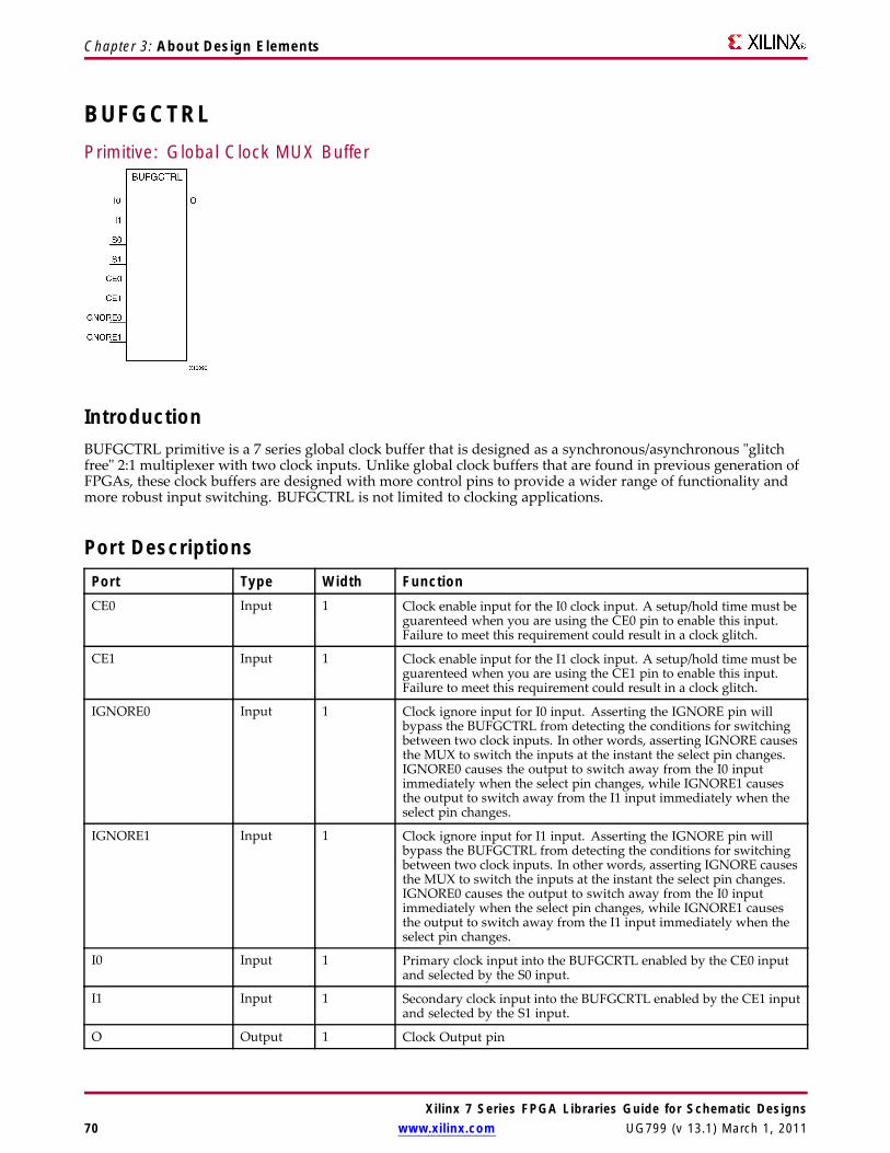
Chapter 3: About Design Elements
BUFGCTRLPrimitive: Global Clock MUX Buffer
IntroductionBUFGCTRL primitive is a 7 series global clock buffer that is designed as a synchronous/asynchronous "glitchfree" 2:1 multiplexer with two clock inputs. Unlike global clock buffers that are found in previous generation ofFPGAs, these clock buffers are designed with more control pins to provide a wider range of functionality andmore robust input switching. BUFGCTRL is not limited to clocking applications.
Port DescriptionsPort Type Width FunctionCE0 Input 1 Clock enable input for the I0 clock input. A setup/hold time must be
guarenteed when you are using the CE0 pin to enable this input.Failure to meet this requirement could result in a clock glitch.
CE1 Input 1 Clock enable input for the I1 clock input. A setup/hold time must beguarenteed when you are using the CE1 pin to enable this input.Failure to meet this requirement could result in a clock glitch.
IGNORE0 Input 1 Clock ignore input for I0 input. Asserting the IGNORE pin willbypass the BUFGCTRL from detecting the conditions for switchingbetween two clock inputs. In other words, asserting IGNORE causesthe MUX to switch the inputs at the instant the select pin changes.IGNORE0 causes the output to switch away from the I0 inputimmediately when the select pin changes, while IGNORE1 causesthe output to switch away from the I1 input immediately when theselect pin changes.
IGNORE1 Input 1 Clock ignore input for I1 input. Asserting the IGNORE pin willbypass the BUFGCTRL from detecting the conditions for switchingbetween two clock inputs. In other words, asserting IGNORE causesthe MUX to switch the inputs at the instant the select pin changes.IGNORE0 causes the output to switch away from the I0 inputimmediately when the select pin changes, while IGNORE1 causesthe output to switch away from the I1 input immediately when theselect pin changes.
I0 Input 1 Primary clock input into the BUFGCRTL enabled by the CE0 inputand selected by the S0 input.
I1 Input 1 Secondary clock input into the BUFGCRTL enabled by the CE1 inputand selected by the S1 input.
O Output 1 Clock Output pin
Xilinx 7 Series FPGA Libraries Guide for Schematic Designs70 www.xilinx.com UG799 (v 13.1) March 1, 2011

Chapter 3: About Design Elements
Port Type Width FunctionS0 Input 1 Clock select input for I0. The S pins represent the clock select pin
for each clock inputs. When using the S pin as input select, there isa setup/hold time requirement. Unlike CE pins, failure to meet thisrequirement wont result in a clock glitch. However, it can cause theoutput clock to appear one clock cycle later.
S1 Input 1 Clock select input for I1. The S pins represent the clock select pinfor each clock inputs. When using the S pin as input select, there isa setup/hold time requirement. Unlike CE pins, failure to meet thisrequirement wont result in a clock glitch. However, it can cause theoutput clock to appear one clock cycle later.
Design Entry MethodThis design element can be used in schematics.
Available Attributes
Attribute TypeAllowedValues Default Description
INIT_OUT DECIMAL 0, 1 0 Initializes the BUFGCTRL output to the specifiedvalue after configuration.
PRESELECT_I0 BOOLEAN “FALSE”,“TRUE”
“FALSE” If “TRUE”, BUFGCTRL output uses I0 input afterconfiguration.
PRESELECT_I1 BOOLEAN “FALSE”,“TRUE”
“FALSE” If “TRUE”, BUFGCTRL output uses I1 input afterconfiguration.
Note Both PRESELECT attributes might not be TRUE at the same time.
For More InformationSee the 7 series FPGA User Documentation (User Guides and Data Sheets).
Xilinx 7 Series FPGA Libraries Guide for Schematic DesignsUG799 (v 13.1) March 1, 2011 www.xilinx.com 71

Xilinx 7 Series FPGA Libraries Guide for Schematic Designs72 www.xilinx.com UG799 (v 13.1) March 1, 2011

Chapter 3: About Design Elements
BUFGMUX_CTRLPrimitive: 2-to-1 Global Clock MUX Buffer
IntroductionThis design element is a global clock buffer with two clock inputs, one clock output, and a select line used tocleanly select between one of two clocks driving the global clocking resource. This component is based onBUFGCTRL, with some pins connected to logic High or Low. This element uses the S pin as the select pin for the2-to-1 MUX. S can switch anytime without causing a glitch on the output clock of the buffer.
Port DescriptionsPort Direction Width FunctionO Output 1 bit Clock Output
I0 Input 1 bit One of two Clock Inputs
I1 Input 1 bit One of two Clock Inputs
S Input 1 bit Select for I0 (S=0) or I1 (S=1)Clock Output
Design Entry MethodThis design element can be used in schematics.
For More InformationSee the 7 series FPGA User Documentation (User Guides and Data Sheets).
Xilinx 7 Series FPGA Libraries Guide for Schematic DesignsUG799 (v 13.1) March 1, 2011 www.xilinx.com 73
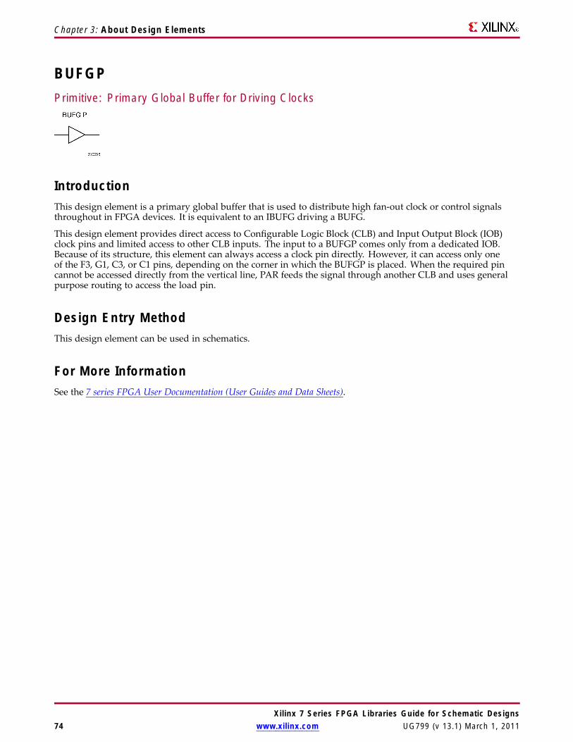
Chapter 3: About Design Elements
BUFGPPrimitive: Primary Global Buffer for Driving Clocks
IntroductionThis design element is a primary global buffer that is used to distribute high fan-out clock or control signalsthroughout in FPGA devices. It is equivalent to an IBUFG driving a BUFG.
This design element provides direct access to Configurable Logic Block (CLB) and Input Output Block (IOB)clock pins and limited access to other CLB inputs. The input to a BUFGP comes only from a dedicated IOB.Because of its structure, this element can always access a clock pin directly. However, it can access only oneof the F3, G1, C3, or C1 pins, depending on the corner in which the BUFGP is placed. When the required pincannot be accessed directly from the vertical line, PAR feeds the signal through another CLB and uses generalpurpose routing to access the load pin.
Design Entry MethodThis design element can be used in schematics.
For More InformationSee the 7 series FPGA User Documentation (User Guides and Data Sheets).
Xilinx 7 Series FPGA Libraries Guide for Schematic Designs74 www.xilinx.com UG799 (v 13.1) March 1, 2011

Chapter 3: About Design Elements
BUFHPrimitive: Clock buffer for a single clocking region
IntroductionThe BUFH primitive is provided to allow instantiation capability to access the HCLK clock buffer resources.The use of this component requires manual placement and special consideration and thus is recommended formore advanced users. Please refer to the 7 series FPGA Clocking Resources User Guide (UG362) for details inusing this component.
Port DescriptionsPort Type Width FunctionI Input 1 Clock Input
O Output 1 Clock Output
Design Entry MethodThis design element can be used in schematics.
For More InformationSee the 7 series FPGA User Documentation (User Guides and Data Sheets).
Xilinx 7 Series FPGA Libraries Guide for Schematic DesignsUG799 (v 13.1) March 1, 2011 www.xilinx.com 75

Chapter 3: About Design Elements
BUFHCEPrimitive: HROW Clock Buffer for a Single Clocking Region with Clock Enable
IntroductionThe BUFHCE primitive allows direct access to the clock region entry point of the global buffer (BUFG) resource.This allows access to unused portions of the global clocking network to be used as high-speed, low skew local(single clock region) routing resources. Additionally, the CE or clock enable input allows for finer-grained controlof clock enabling or gating to allow for power reduction for circuitry or portions of the design not constantlyused. Please refer to the 7 series FPGA Clocking Resources User Guide for details for using this component.
Port DescriptionsPort Type Width FunctionCE Input 1 Enables propagation of signal from I to O. When low, performs a
glitchless transition of the output to INIT_OUT value.
I Input 1 Clock Input.
O Output 1 Clock Output.
Design Entry MethodThis design element can be used in schematics.
Available AttributesAttribute Type Allowed Values Default DescriptionCE_TYPE STRING “SYNC”,
“ASYNC”“SYNC” Sets clock enable behavior where "SYNC" allows for
a glitchless transition to and from the INIT_OUTvalue. "ASYNC" is generally used to create a moreimmediate transition such as when you can expectthe clock to be stopped or when using the BUFHCEfor a high fanout control or data path routing insteadof a clock buffer.
INIT_OUT DECIMAL 0, 1 0 Initial output value, also indicates stop low vs stophigh behavior.
For More InformationSee the 7 series FPGA User Documentation (User Guides and Data Sheets).
Xilinx 7 Series FPGA Libraries Guide for Schematic Designs76 www.xilinx.com UG799 (v 13.1) March 1, 2011

Chapter 3: About Design Elements
BUFIOPrimitive: Local Clock Buffer for I/O
IntroductionThis design element is simply a clock-in, clock-out buffer. It drives a dedicated clock net within the I/O column,independent of the global clock resources. Thus, these elements are ideally suited for source-synchronous datacapture (forwarded/receiver clock distribution). For Single IO Bank applications the BUFIO can be sourced bya MRCC or SRCC I/O. If the BUFIO connects to I/Os in more than one I/O Bank then a MRCC (Multi RegionClock Capable I/O) pin must be used. The MRCC will connect to a dedicated BUFMRCE/BUFMR capable ofdriving BUFIOs in the same clock region, the clock region above, and the clock region below. They can bedriven by a dedicated MRCC I/O located in the same clock region or a BUFMRCE/BUFMR component capableof clocking multiple clock regions. The BUFIO can only drive I/O components within the bank in which theyexist. These elements cannot directly drive logic resources (CLB, block RAM, etc.) because the I/O clock networkonly reaches the I/O column.
Port DescriptionsPort Type Width FunctionI Input 1 Input port to clock buffer. Connect this to
an IBUFG connected to a top-level port oran associated BUFMR buffer.
O Output 1 Output port from clock buffer. Connectthis to the clock inputs to synchronousI/O components like the ISERDESE2,OSERDESE2, IDDR, ODDR or a registerconnected directly to an I/O port (inferredor instantiated).
Design Entry MethodThis design element can be used in schematics.
For More InformationSee the 7 series FPGA User Documentation (User Guides and Data Sheets).
Xilinx 7 Series FPGA Libraries Guide for Schematic DesignsUG799 (v 13.1) March 1, 2011 www.xilinx.com 77

Chapter 3: About Design Elements
BUFIODQSPrimitive: Differential Clock Input for Transceiver Reference Clocks
IntroductionThis element is the same clock buffer as BUFIO with added dedicated circuitry (ideally used for memoryapplications) to optionally remove the extra BUFIO delay and also squelch the I/O Clock after a given burstlength from the strobe. In general, this component should only be used with the Xilinx® Memory InterfaceGenerator (MIG) product.
Port DescriptionsPort Type Width FunctionDQSMASK Input 1 "Squelch" the I/O clock after a given burst length
from strobe.
I Input 1 Clock input port.
O Output 1 Clock output port.
Design Entry MethodThis design element can be used in schematics.
Available AttributesAttribute Type Allowed Values Default DescriptionDQSMASK_ENABLE Boolean FALSE, TRUE FALSE Enables the squelch circuitry
For More InformationSee the 7 series FPGA User Documentation (User Guides and Data Sheets).
Xilinx 7 Series FPGA Libraries Guide for Schematic Designs78 www.xilinx.com UG799 (v 13.1) March 1, 2011
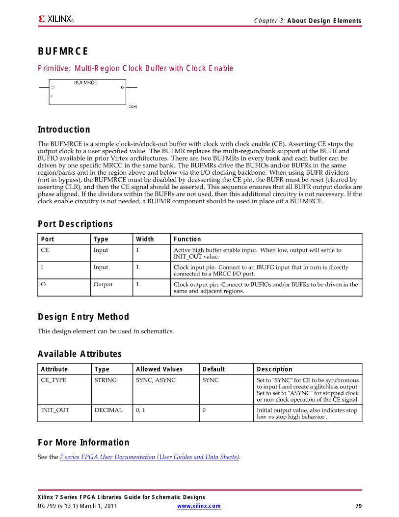
Chapter 3: About Design Elements
BUFMRCEPrimitive: Multi-Region Clock Buffer with Clock Enable
IntroductionThe BUFMRCE is a simple clock-in/clock-out buffer with clock with clock enable (CE). Asserting CE stops theoutput clock to a user specified value. The BUFMR replaces the multi-region/bank support of the BUFR andBUFIO available in prior Virtex architectures. There are two BUFMRs in every bank and each buffer can bedriven by one specific MRCC in the same bank. The BUFMRs drive the BUFIOs and/or BUFRs in the sameregion/banks and in the region above and below via the I/O clocking backbone. When using BUFR dividers(not in bypass), the BUFMRCE must be disabled by deasserting the CE pin, the BUFR must be reset (cleared byasserting CLR), and then the CE signal should be asserted. This sequence ensures that all BUFR output clocks arephase aligned. If the dividers within the BUFRs are not used, then this additional circuitry is not necessary. If theclock enable circuitry is not needed, a BUFMR component should be used in place oif a BUFMRCE.
Port DescriptionsPort Type Width FunctionCE Input 1 Active high buffer enable input. When low, output will settle to
INIT_OUT value.
I Input 1 Clock input pin. Connect to an IBUFG input that in turn is directlyconnected to a MRCC I/O port.
O Output 1 Clock output pin. Connect to BUFIOs and/or BUFRs to be driven in thesame and adjacent regions.
Design Entry MethodThis design element can be used in schematics.
Available AttributesAttribute Type Allowed Values Default DescriptionCE_TYPE STRING SYNC, ASYNC SYNC Set to "SYNC" for CE to be synchronous
to input I and create a glitchless output.Set to set to "ASYNC" for stopped clockor non-clock operation of the CE signal.
INIT_OUT DECIMAL 0, 1 0 Initial output value, also indicates stoplow vs stop high behavior .
For More InformationSee the 7 series FPGA User Documentation (User Guides and Data Sheets).
Xilinx 7 Series FPGA Libraries Guide for Schematic DesignsUG799 (v 13.1) March 1, 2011 www.xilinx.com 79

Chapter 3: About Design Elements
BUFRPrimitive: Regional Clock Buffer for I/O and Logic Resources within a Clock Region
IntroductionThe BUFR is a regional clock buffer available in 7 series devices. BUFRs drive clock signals to a dedicated clocknet within a clock region, independent from the global clock tree. Each BUFR can drive the regional clock nets inthe region in which it is located. Unlike BUFIOs, BUFRs can drive the I/O logic and logic resources (CLB, blockRAM, etc.) in the existing clock region. BUFRs can be driven by either the output from an IBUFG, BUFMRCE,MMCM or local interconnect. In addition, BUFRs are capable of generating divided clock outputs with respect tothe clock input. The divide value is an integer between one and eight. BUFRs are ideal for source-synchronousapplications requiring clock domain crossing or serial-to-parallel conversion. There are two BUFRs in a typicalclock region (two regional clock networks). If local clocking is needed in multiple clock regions, the BUFMRCEcan drive multiple BUFRs in adjacent clock regions to further extend this clocking capability. Please refer tothe BUFMRCE for more details.
Port DescriptionsPort Type Width FunctionCE Input 1 Clock enable port. When asserted Low, this port disables the output
clock at port O. When asserted High, this port resets the counter usedto produce the divided clock output.
CLR Input 1 Counter reset for divided clock output. When asserted High, thisport resets the counter used to produce the divided clock output.
I Input 1 Clock input port. This port is the clock source port for BUFR. It canbe driven by an IBUFG, BUFMRCE, MMCM, or local interconnect.
O Output 1 Clock output port. This port drives the clock tracks in the clockregion of the BUFR and the two adjacent clock regions. This portconnects to FPGA clocked components.
Design Entry MethodThis design element can be used in schematics.
Available AttributesAttribute Type Allowed_Values Default DescriptionBUFR_DIVIDE STRING BYPASS, 1, 2, 3, 4, 5, 6, 7,
8BYPASS Defines whether the output clock is a
divided version of input clock.
SIM_DEVICE STRING VIRTEX4, 7SERIES,VIRTEX5, VIRTEX6
VIRTEX4 For correct simulation behavior, thisattribute must be set to "7SERIES".
For More InformationSee the 7 series FPGA User Documentation (User Guides and Data Sheets).
Xilinx 7 Series FPGA Libraries Guide for Schematic Designs80 www.xilinx.com UG799 (v 13.1) March 1, 2011

Chapter 3: About Design Elements
CAPTUREE2Primitive: Register Capture
IntroductionThis element provides user control and synchronization over when and how the capture register (flip-flop andlatch) information task is requested. The readback function is provided through dedicated configuration portinstructions. However, without this element, the readback data is synchronized to the configuration clock.Only register (flip-flop and latch) states can be captured. Although LUT RAM, SRL, and block RAM states arereadback, they cannot be captured. An asserted high CAP signal indicates that the registers in the device areto be captured at the next Low-to-High clock transition. By default, data is captured after every trigger whentransition on CLK while CAP is asserted. To limit the readback operation to a single data capture, add theONESHOT=TRUE attribute to this element.
Port DescriptionsPort Type Width FunctionCAP Input 1 Capture Input
CLK Input 1 Clock Input
Design Entry MethodThis design element can be used in schematics.
Available AttributesAttribute Type Allowed Values Default DescriptionONESHOT STRING “TRUE”, “FALSE” “TRUE” Specifies the procedure for performing
single readback per CAP trigger.Possible Values: "TRUE" or "FALSE"
For More Information• See the 7 series FPGA SelectIO Resources User Guide.
• See the 7 series FPGA Data Sheet DC and Switching Characteristics.
Xilinx 7 Series FPGA Libraries Guide for Schematic DesignsUG799 (v 13.1) March 1, 2011 www.xilinx.com 81

Chapter 3: About Design Elements
CARRY4Primitive: Fast Carry Logic with Look Ahead
IntroductionThis circuit design represents the fast carry logic for a slice. The carry chain consists of a series of four MUXsand four XORs that connect to the other logic (LUTs) in the slice via dedicated routes to form more complexfunctions. The fast carry logic is useful for building arithmetic functions like adders, counters, subtractors andadd/subs, as well as such other logic functions as wide comparators, address decoders, and some logic gates(specifically, AND and OR).
Port DescriptionsPort Direction Width FunctionO Output 4 Carry chain XOR general data out
CO Output 4 Carry-out of each stage of the carry chain
DI Input 4 Carry-MUX data input
S Input 4 Carry-MUX select line
CYINIT Input 1 Carry-in initialization input
CI Input 1 Carry cascade input
Design Entry MethodThis design element can be used in schematics.
For More InformationSee the 7 series FPGA User Documentation (User Guides and Data Sheets).
Xilinx 7 Series FPGA Libraries Guide for Schematic Designs82 www.xilinx.com UG799 (v 13.1) March 1, 2011

Chapter 3: About Design Elements
CB16CEMacro: 16-Bit Cascadable Binary Counter with Clock Enable and Asynchronous Clear
IntroductionThis design element is an asynchronously clearable, cascadable binary counter. The asynchronous clear (CLR)input, when High, overrides all other inputs and forces the Q outputs, terminal count (TC), and clock enable out(CEO) to logic level zero, independent of clock transitions. The Q outputs increment when the clock enable input(CE) is High during the Low-to-High clock (C) transition. The counter ignores clock transitions when CE is Low.The TC output is High when all Q outputs are High.
Create larger counters by connecting the CEO output of each stage to the CE input of the next stage andconnecting the C and CLR inputs in parallel. CEO is active (High) when TC and CE are High. The maximumlength of the counter is determined by the accumulated CE-to-TC propagation delays versus the clock period.The clock period must be greater than n (tCE-TC), where n is the number of stages and the time tCE-TC is theCE-to-TC propagation delay of each stage. When cascading counters, use the CEO output if the counter uses theCE input or use the TC output if it does not.
This counter is asynchronously cleared, outputs Low, when power is applied. For FPGA devices, power-onconditions are simulated when global set/reset (GSR) is active. GSR defaults to active-High but can be invertedby adding an inverter in front of the GSR input of the appropriate STARTUP_architecture symbol.
Logic TableInputs Outputs
CLR CE C Qz-Q0 TC CEO1 X X 0 0 0
0 0 X No change No change 0
0 1 ↑ Inc TC CEO
z = bit width - 1
TC = Qz•Q(z-1)•Q(z-2)•...•Q0
CEO = TC•CE
Design Entry MethodThis design element is only for use in schematics.
For More InformationSee the 7 series FPGA User Documentation (User Guides and Data Sheets).
Xilinx 7 Series FPGA Libraries Guide for Schematic DesignsUG799 (v 13.1) March 1, 2011 www.xilinx.com 83

Xilinx 7 Series FPGA Libraries Guide for Schematic Designs84 www.xilinx.com UG799 (v 13.1) March 1, 2011

Chapter 3: About Design Elements
CB16CLEMacro: 16-Bit Loadable Cascadable Binary Counters with Clock Enable and AsynchronousClear
IntroductionThis element is a synchronously loadable, asynchronously clearable, cascadable binary counter. Theasynchronous clear (CLR) input, when High, overrides all other inputs and forces the Q outputs, terminalcount (TC), and clock enable out (CEO) to logic level zero, independent of clock transitions. The data on theD inputs is loaded into the counter when the load enable input (L) is High during the Low-to-High clocktransition, independent of the state of clock enable (CE). The Q outputs increment when CE is High during theLow-to-High clock transition. The counter ignores clock transitions when CE is Low. The TC output is Highwhen all Q outputs are High.
Create larger counters by connecting the CEO output of each stage to the CE input of the next stage andconnecting the C, L, and CLR inputs in parallel. CEO is active (High) when TC and CE are High. The maximumlength of the counter is determined by the accumulated CE-to-TC propagation delays versus the clock period.The clock period must be greater than n (tCE-TC), where n is the number of stages and the time tCE-TC is theCE-to-TC propagation delay of each stage. When cascading counters, use the CEO output if the counter uses theCE input or use the TC output if it does not.
This counter is asynchronously cleared, outputs Low, when power is applied. For FPGA devices, power-onconditions are simulated when global set/reset (GSR) is active. GSR defaults to active-High but can be invertedby adding an inverter in front of the GSR input of the appropriate STARTUP_architecture symbol.
Xilinx 7 Series FPGA Libraries Guide for Schematic DesignsUG799 (v 13.1) March 1, 2011 www.xilinx.com 85

Chapter 3: About Design Elements
Logic TableInputs Outputs
CLR L CE C Dz-D0 Qz-Q0 TC CEO1 X X X X 0 0 0
0 1 X ↑ Dn Dn TC CEO
0 0 0 X X No change No change 0
0 0 1 ↑ X Inc TC CEO
z = bit width - 1
TC = Qz•Q(z-1)•Q(z-2)•...•Q0
CEO = TC•CE
Design Entry MethodThis design element is only for use in schematics.
For More InformationSee the 7 series FPGA User Documentation (User Guides and Data Sheets).
Xilinx 7 Series FPGA Libraries Guide for Schematic Designs86 www.xilinx.com UG799 (v 13.1) March 1, 2011

Chapter 3: About Design Elements
CB16CLEDMacro: 16-Bit Loadable Cascadable Bidirectional Binary Counters with Clock Enableand Asynchronous Clear
IntroductionThis design element is a synchronously loadable, asynchronously clearable, cascadable, bidirectional binarycounter. The asynchronous clear (CLR) input, when High, overrides all other inputs and forces the Q outputs,terminal count (TC), and clock enable out (CEO) to logic level zero, independent of clock transitions. The data onthe D inputs is loaded into the counter when the load enable input (L) is High during the Low-to-High clock(C) transition, independent of the state of clock enable (CE). The Q outputs decrement when CE is High andUP is Low during the Low-to- High clock transition. The Q outputs increment when CE and UP are High. Thecounter ignores clock transitions when CE is Low.
For counting up, the TC output is High when all Q outputs and UP are High. For counting down, the TCoutput is High when all Q outputs and UP are Low.
Create larger counters by connecting the CEO output of each stage to the CE input of the next stage andconnecting the C, UP, L, and CLR inputs in parallel. CEO is active (High) when TC and CE are High. Themaximum length of the counter is determined by the accumulated CE-to-TC propagation delays versus the clockperiod. The clock period must be greater than n (tCE-TC), where n is the number of stages and the time tCE-TC isthe CE-to-TC propagation delay of each stage. When cascading counters, use the CEO output if the counteruses the CE input or use the TC output if it does not.
For CPLD parts, see “CB2X1”, “CB4X1”, “CB8X1”, “CB16X1” for high-performance cascadable, bidirectionalcounters.
This counter is asynchronously cleared, outputs Low, when power is applied. For FPGA devices, power-onconditions are simulated when global set/reset (GSR) is active. GSR defaults to active-High but can be invertedby adding an inverter in front of the GSR input of the appropriate STARTUP_architecture symbol.
Xilinx 7 Series FPGA Libraries Guide for Schematic DesignsUG799 (v 13.1) March 1, 2011 www.xilinx.com 87

Chapter 3: About Design Elements
Logic TableInputs Outputs
CLR L CE C UP Dz-D0 Qz-Q0 TC CEO1 X X X X X 0 0 0
0 1 X ↑ X Dn Dn TC CEO
0 0 0 X X X No change No change 0
0 0 1 ↑ 1 X Inc TC CEO
0 0 1 ↑ 0 X Dec TC CEO
z = bit width - 1
TC = (Qz•Q(z-1)•Q(z-2)•...•Q0•UP) + (Qz•Q(z-1)•Q(z-2)•...•Q0•UP)
CEO = TC•CE
Design Entry MethodThis design element is only for use in schematics.
For More InformationSee the 7 series FPGA User Documentation (User Guides and Data Sheets).
Xilinx 7 Series FPGA Libraries Guide for Schematic Designs88 www.xilinx.com UG799 (v 13.1) March 1, 2011

Chapter 3: About Design Elements
CB16REMacro: 16-Bit Cascadable Binary Counter with Clock Enable and Synchronous Reset
IntroductionThis design element is a synchronous, resettable, cascadable binary counter. The synchronous reset (R), whenHigh, overrides all other inputs and forces the Q outputs, terminal count (TC), and clock enable out (CEO) tozero on the Low-to-High clock transition. The Q outputs increment when the clock enable input (CE) is Highduring the Low-to-High clock (C) transition. The counter ignores clock transitions when CE is Low. The TCoutput is High when both Q outputs are High.
Create larger counters by connecting the CEO output of each stage to the CE input of the next stage andconnecting the C and R inputs in parallel. CEO is active (High) when TC and CE are High. The maximum lengthof the counter is determined by the accumulated CE-to-TC propagation delays versus the clock period. Theclock period must be greater than n (tCE-TC), where n is the number of stages and the time tCE-TC is the CE-to-TCpropagation delay of each stage. When cascading counters, use the CEO output if the counter uses the CEinput or use the TC output if it does not.
This counter is asynchronously cleared, outputs Low, when power is applied. For FPGA devices, power-onconditions are simulated when global set/reset (GSR) is active. GSR defaults to active-High but can be invertedby adding an inverter in front of the GSR input of the appropriate STARTUP_architecture symbol.
Logic TableInputs Outputs
R CE C Qz-Q0 TC CEO1 X ↑ 0 0 0
0 0 X No change No change 0
0 1 ↑ Inc TC CEO
z = bit width - 1
TC = Qz•Q(z-1)•Q(z-2)•...•Q0)
CEO = TC•CE
Design Entry MethodThis design element is only for use in schematics.
For More InformationSee the 7 series FPGA User Documentation (User Guides and Data Sheets).
Xilinx 7 Series FPGA Libraries Guide for Schematic DesignsUG799 (v 13.1) March 1, 2011 www.xilinx.com 89

Chapter 3: About Design Elements
CB2CEMacro: 2-Bit Cascadable Binary Counter with Clock Enable and Asynchronous Clear
IntroductionThis design element is an asynchronously clearable, cascadable binary counter. The asynchronous clear (CLR)input, when High, overrides all other inputs and forces the Q outputs, terminal count (TC), and clock enable out(CEO) to logic level zero, independent of clock transitions. The Q outputs increment when the clock enable input(CE) is High during the Low-to-High clock (C) transition. The counter ignores clock transitions when CE is Low.The TC output is High when all Q outputs are High.
Create larger counters by connecting the CEO output of each stage to the CE input of the next stage andconnecting the C and CLR inputs in parallel. CEO is active (High) when TC and CE are High. The maximumlength of the counter is determined by the accumulated CE-to-TC propagation delays versus the clock period.The clock period must be greater than n (tCE-TC), where n is the number of stages and the time tCE-TC is theCE-to-TC propagation delay of each stage. When cascading counters, use the CEO output if the counter uses theCE input or use the TC output if it does not.
This counter is asynchronously cleared, outputs Low, when power is applied. For FPGA devices, power-onconditions are simulated when global set/reset (GSR) is active. GSR defaults to active-High but can be invertedby adding an inverter in front of the GSR input of the appropriate STARTUP_architecture symbol.
Logic TableInputs Outputs
CLR CE C Qz-Q0 TC CEO1 X X 0 0 0
0 0 X No change No change 0
0 1 ↑ Inc TC CEO
z = bit width - 1
TC = Qz•Q(z-1)•Q(z-2)•...•Q0
CEO = TC•CE
Design Entry MethodThis design element is only for use in schematics.
For More InformationSee the 7 series FPGA User Documentation (User Guides and Data Sheets).
Xilinx 7 Series FPGA Libraries Guide for Schematic Designs90 www.xilinx.com UG799 (v 13.1) March 1, 2011

Chapter 3: About Design Elements
CB2CLEMacro: 2-Bit Loadable Cascadable Binary Counters with Clock Enable and AsynchronousClear
IntroductionThis element is a synchronously loadable, asynchronously clearable, cascadable binary counter. Theasynchronous clear (CLR) input, when High, overrides all other inputs and forces the Q outputs, terminalcount (TC), and clock enable out (CEO) to logic level zero, independent of clock transitions. The data on theD inputs is loaded into the counter when the load enable input (L) is High during the Low-to-High clocktransition, independent of the state of clock enable (CE). The Q outputs increment when CE is High during theLow-to-High clock transition. The counter ignores clock transitions when CE is Low. The TC output is Highwhen all Q outputs are High.
Create larger counters by connecting the CEO output of each stage to the CE input of the next stage andconnecting the C, L, and CLR inputs in parallel. CEO is active (High) when TC and CE are High. The maximumlength of the counter is determined by the accumulated CE-to-TC propagation delays versus the clock period.The clock period must be greater than n (tCE-TC), where n is the number of stages and the time tCE-TC is theCE-to-TC propagation delay of each stage. When cascading counters, use the CEO output if the counter uses theCE input or use the TC output if it does not.
This counter is asynchronously cleared, outputs Low, when power is applied. For FPGA devices, power-onconditions are simulated when global set/reset (GSR) is active. GSR defaults to active-High but can be invertedby adding an inverter in front of the GSR input of the appropriate STARTUP_architecture symbol.
Logic TableInputs Outputs
CLR L CE C Dz-D0 Qz-Q0 TC CEO1 X X X X 0 0 0
0 1 X ↑ Dn Dn TC CEO
0 0 0 X X No change No change 0
0 0 1 ↑ X Inc TC CEO
z = bit width - 1
TC = Qz•Q(z-1)•Q(z-2)•...•Q0
CEO = TC•CE
Design Entry MethodThis design element is only for use in schematics.
Xilinx 7 Series FPGA Libraries Guide for Schematic DesignsUG799 (v 13.1) March 1, 2011 www.xilinx.com 91

Chapter 3: About Design Elements
For More InformationSee the 7 series FPGA User Documentation (User Guides and Data Sheets).
Xilinx 7 Series FPGA Libraries Guide for Schematic Designs92 www.xilinx.com UG799 (v 13.1) March 1, 2011

Chapter 3: About Design Elements
CB2CLEDMacro: 2-Bit Loadable Cascadable Bidirectional Binary Counters with Clock Enable andAsynchronous Clear
IntroductionThis design element is a synchronously loadable, asynchronously clearable, cascadable, bidirectional binarycounter. The asynchronous clear (CLR) input, when High, overrides all other inputs and forces the Q outputs,terminal count (TC), and clock enable out (CEO) to logic level zero, independent of clock transitions. The data onthe D inputs is loaded into the counter when the load enable input (L) is High during the Low-to-High clock(C) transition, independent of the state of clock enable (CE). The Q outputs decrement when CE is High andUP is Low during the Low-to- High clock transition. The Q outputs increment when CE and UP are High. Thecounter ignores clock transitions when CE is Low.
For counting up, the TC output is High when all Q outputs and UP are High. For counting down, the TCoutput is High when all Q outputs and UP are Low.
Create larger counters by connecting the CEO output of each stage to the CE input of the next stage andconnecting the C, UP, L, and CLR inputs in parallel. CEO is active (High) when TC and CE are High. Themaximum length of the counter is determined by the accumulated CE-to-TC propagation delays versus the clockperiod. The clock period must be greater than n (tCE-TC), where n is the number of stages and the time tCE-TC isthe CE-to-TC propagation delay of each stage. When cascading counters, use the CEO output if the counteruses the CE input or use the TC output if it does not.
For CPLD parts, see “CB2X1”, “CB4X1”, “CB8X1”, “CB16X1” for high-performance cascadable, bidirectionalcounters.
This counter is asynchronously cleared, outputs Low, when power is applied. For FPGA devices, power-onconditions are simulated when global set/reset (GSR) is active. GSR defaults to active-High but can be invertedby adding an inverter in front of the GSR input of the appropriate STARTUP_architecture symbol.
Xilinx 7 Series FPGA Libraries Guide for Schematic DesignsUG799 (v 13.1) March 1, 2011 www.xilinx.com 93

Chapter 3: About Design Elements
Logic TableInputs Outputs
CLR L CE C UP Dz-D0 Qz-Q0 TC CEO1 X X X X X 0 0 0
0 1 X ↑ X Dn Dn TC CEO
0 0 0 X X X No change No change 0
0 0 1 ↑ 1 X Inc TC CEO
0 0 1 ↑ 0 X Dec TC CEO
z = bit width - 1
TC = (Qz•Q(z-1)•Q(z-2)•...•Q0•UP) + (Qz•Q(z-1)•Q(z-2)•...•Q0•UP)
CEO = TC•CE
Design Entry MethodThis design element is only for use in schematics.
For More InformationSee the 7 series FPGA User Documentation (User Guides and Data Sheets).
Xilinx 7 Series FPGA Libraries Guide for Schematic Designs94 www.xilinx.com UG799 (v 13.1) March 1, 2011

Chapter 3: About Design Elements
CB2REMacro: 2-Bit Cascadable Binary Counter with Clock Enable and Synchronous Reset
IntroductionThis design element is a synchronous, resettable, cascadable binary counter. The synchronous reset (R), whenHigh, overrides all other inputs and forces the Q outputs, terminal count (TC), and clock enable out (CEO) tozero on the Low-to-High clock transition. The Q outputs increment when the clock enable input (CE) is Highduring the Low-to-High clock (C) transition. The counter ignores clock transitions when CE is Low. The TCoutput is High when both Q outputs are High.
Create larger counters by connecting the CEO output of each stage to the CE input of the next stage andconnecting the C and R inputs in parallel. CEO is active (High) when TC and CE are High. The maximum lengthof the counter is determined by the accumulated CE-to-TC propagation delays versus the clock period. Theclock period must be greater than n (tCE-TC), where n is the number of stages and the time tCE-TC is the CE-to-TCpropagation delay of each stage. When cascading counters, use the CEO output if the counter uses the CEinput or use the TC output if it does not.
This counter is asynchronously cleared, outputs Low, when power is applied. For FPGA devices, power-onconditions are simulated when global set/reset (GSR) is active. GSR defaults to active-High but can be invertedby adding an inverter in front of the GSR input of the appropriate STARTUP_architecture symbol.
Logic TableInputs Outputs
R CE C Qz-Q0 TC CEO1 X ↑ 0 0 0
0 0 X No change No change 0
0 1 ↑ Inc TC CEO
z = bit width - 1
TC = Qz•Q(z-1)•Q(z-2)•...•Q0)
CEO = TC•CE
Design Entry MethodThis design element is only for use in schematics.
For More InformationSee the 7 series FPGA User Documentation (User Guides and Data Sheets).
Xilinx 7 Series FPGA Libraries Guide for Schematic DesignsUG799 (v 13.1) March 1, 2011 www.xilinx.com 95

Chapter 3: About Design Elements
CB4CEMacro: 4-Bit Cascadable Binary Counter with Clock Enable and Asynchronous Clear
IntroductionThis design element is an asynchronously clearable, cascadable binary counter. The asynchronous clear (CLR)input, when High, overrides all other inputs and forces the Q outputs, terminal count (TC), and clock enable out(CEO) to logic level zero, independent of clock transitions. The Q outputs increment when the clock enable input(CE) is High during the Low-to-High clock (C) transition. The counter ignores clock transitions when CE is Low.The TC output is High when all Q outputs are High.
Create larger counters by connecting the CEO output of each stage to the CE input of the next stage andconnecting the C and CLR inputs in parallel. CEO is active (High) when TC and CE are High. The maximumlength of the counter is determined by the accumulated CE-to-TC propagation delays versus the clock period.The clock period must be greater than n (tCE-TC), where n is the number of stages and the time tCE-TC is theCE-to-TC propagation delay of each stage. When cascading counters, use the CEO output if the counter uses theCE input or use the TC output if it does not.
This counter is asynchronously cleared, outputs Low, when power is applied. For FPGA devices, power-onconditions are simulated when global set/reset (GSR) is active. GSR defaults to active-High but can be invertedby adding an inverter in front of the GSR input of the appropriate STARTUP_architecture symbol.
Logic TableInputs Outputs
CLR CE C Qz-Q0 TC CEO1 X X 0 0 0
0 0 X No change No change 0
0 1 ↑ Inc TC CEO
z = bit width - 1
TC = Qz•Q(z-1)•Q(z-2)•...•Q0
CEO = TC•CE
Design Entry MethodThis design element is only for use in schematics.
For More InformationSee the 7 series FPGA User Documentation (User Guides and Data Sheets).
Xilinx 7 Series FPGA Libraries Guide for Schematic Designs96 www.xilinx.com UG799 (v 13.1) March 1, 2011
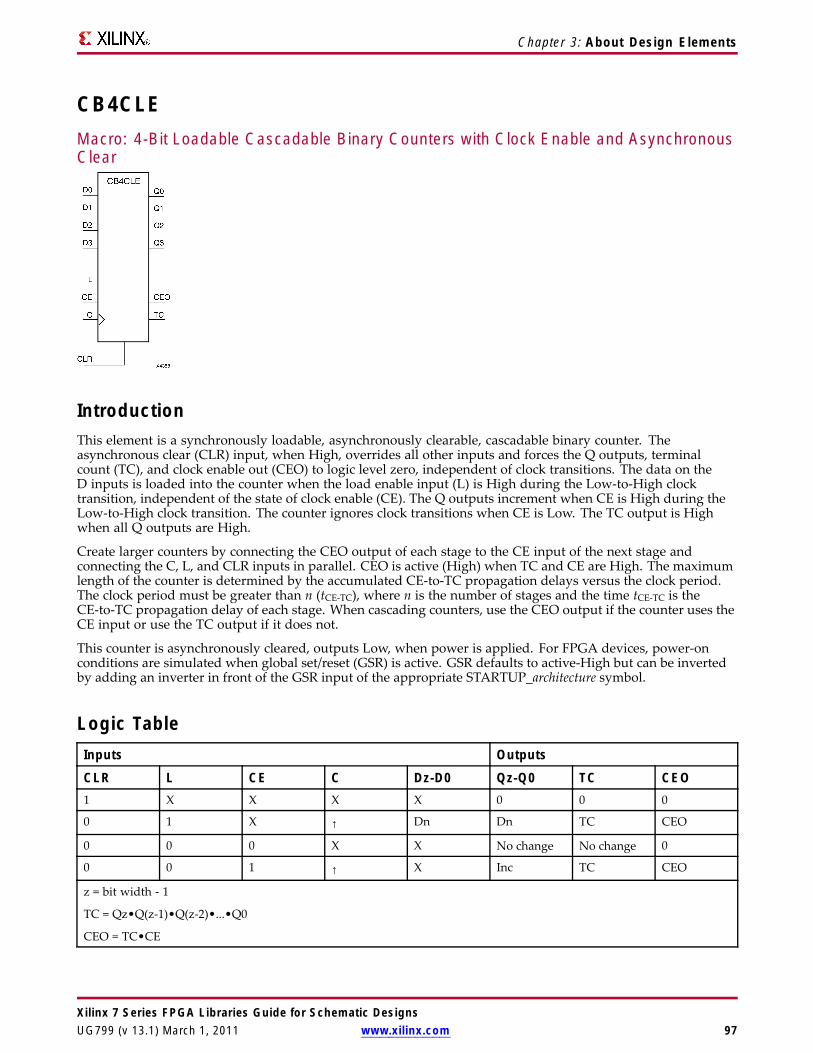
Chapter 3: About Design Elements
CB4CLEMacro: 4-Bit Loadable Cascadable Binary Counters with Clock Enable and AsynchronousClear
IntroductionThis element is a synchronously loadable, asynchronously clearable, cascadable binary counter. Theasynchronous clear (CLR) input, when High, overrides all other inputs and forces the Q outputs, terminalcount (TC), and clock enable out (CEO) to logic level zero, independent of clock transitions. The data on theD inputs is loaded into the counter when the load enable input (L) is High during the Low-to-High clocktransition, independent of the state of clock enable (CE). The Q outputs increment when CE is High during theLow-to-High clock transition. The counter ignores clock transitions when CE is Low. The TC output is Highwhen all Q outputs are High.
Create larger counters by connecting the CEO output of each stage to the CE input of the next stage andconnecting the C, L, and CLR inputs in parallel. CEO is active (High) when TC and CE are High. The maximumlength of the counter is determined by the accumulated CE-to-TC propagation delays versus the clock period.The clock period must be greater than n (tCE-TC), where n is the number of stages and the time tCE-TC is theCE-to-TC propagation delay of each stage. When cascading counters, use the CEO output if the counter uses theCE input or use the TC output if it does not.
This counter is asynchronously cleared, outputs Low, when power is applied. For FPGA devices, power-onconditions are simulated when global set/reset (GSR) is active. GSR defaults to active-High but can be invertedby adding an inverter in front of the GSR input of the appropriate STARTUP_architecture symbol.
Logic TableInputs Outputs
CLR L CE C Dz-D0 Qz-Q0 TC CEO1 X X X X 0 0 0
0 1 X ↑ Dn Dn TC CEO
0 0 0 X X No change No change 0
0 0 1 ↑ X Inc TC CEO
z = bit width - 1
TC = Qz•Q(z-1)•Q(z-2)•...•Q0
CEO = TC•CE
Xilinx 7 Series FPGA Libraries Guide for Schematic DesignsUG799 (v 13.1) March 1, 2011 www.xilinx.com 97
Chapter 3: About Design Elements
Design Entry MethodThis design element is only for use in schematics.
For More InformationSee the 7 series FPGA User Documentation (User Guides and Data Sheets).
Xilinx 7 Series FPGA Libraries Guide for Schematic Designs98 www.xilinx.com UG799 (v 13.1) March 1, 2011

Chapter 3: About Design Elements
CB4CLEDMacro: 4-Bit Loadable Cascadable Bidirectional Binary Counters with Clock Enable andAsynchronous Clear
IntroductionThis design element is a synchronously loadable, asynchronously clearable, cascadable, bidirectional binarycounter. The asynchronous clear (CLR) input, when High, overrides all other inputs and forces the Q outputs,terminal count (TC), and clock enable out (CEO) to logic level zero, independent of clock transitions. The data onthe D inputs is loaded into the counter when the load enable input (L) is High during the Low-to-High clock(C) transition, independent of the state of clock enable (CE). The Q outputs decrement when CE is High andUP is Low during the Low-to- High clock transition. The Q outputs increment when CE and UP are High. Thecounter ignores clock transitions when CE is Low.
For counting up, the TC output is High when all Q outputs and UP are High. For counting down, the TCoutput is High when all Q outputs and UP are Low.
Create larger counters by connecting the CEO output of each stage to the CE input of the next stage andconnecting the C, UP, L, and CLR inputs in parallel. CEO is active (High) when TC and CE are High. Themaximum length of the counter is determined by the accumulated CE-to-TC propagation delays versus the clockperiod. The clock period must be greater than n (tCE-TC), where n is the number of stages and the time tCE-TC isthe CE-to-TC propagation delay of each stage. When cascading counters, use the CEO output if the counteruses the CE input or use the TC output if it does not.
For CPLD parts, see “CB2X1”, “CB4X1”, “CB8X1”, “CB16X1” for high-performance cascadable, bidirectionalcounters.
This counter is asynchronously cleared, outputs Low, when power is applied. For FPGA devices, power-onconditions are simulated when global set/reset (GSR) is active. GSR defaults to active-High but can be invertedby adding an inverter in front of the GSR input of the appropriate STARTUP_architecture symbol.
Xilinx 7 Series FPGA Libraries Guide for Schematic DesignsUG799 (v 13.1) March 1, 2011 www.xilinx.com 99

Chapter 3: About Design Elements
Logic TableInputs Outputs
CLR L CE C UP Dz-D0 Qz-Q0 TC CEO1 X X X X X 0 0 0
0 1 X ↑ X Dn Dn TC CEO
0 0 0 X X X No change No change 0
0 0 1 ↑ 1 X Inc TC CEO
0 0 1 ↑ 0 X Dec TC CEO
z = bit width - 1
TC = (Qz•Q(z-1)•Q(z-2)•...•Q0•UP) + (Qz•Q(z-1)•Q(z-2)•...•Q0•UP)
CEO = TC•CE
Design Entry MethodThis design element is only for use in schematics.
For More InformationSee the 7 series FPGA User Documentation (User Guides and Data Sheets).
Xilinx 7 Series FPGA Libraries Guide for Schematic Designs100 www.xilinx.com UG799 (v 13.1) March 1, 2011

Chapter 3: About Design Elements
CB4REMacro: 4-Bit Cascadable Binary Counter with Clock Enable and Synchronous Reset
IntroductionThis design element is a synchronous, resettable, cascadable binary counter. The synchronous reset (R), whenHigh, overrides all other inputs and forces the Q outputs, terminal count (TC), and clock enable out (CEO) tozero on the Low-to-High clock transition. The Q outputs increment when the clock enable input (CE) is Highduring the Low-to-High clock (C) transition. The counter ignores clock transitions when CE is Low. The TCoutput is High when both Q outputs are High.
Create larger counters by connecting the CEO output of each stage to the CE input of the next stage andconnecting the C and R inputs in parallel. CEO is active (High) when TC and CE are High. The maximum lengthof the counter is determined by the accumulated CE-to-TC propagation delays versus the clock period. Theclock period must be greater than n (tCE-TC), where n is the number of stages and the time tCE-TC is the CE-to-TCpropagation delay of each stage. When cascading counters, use the CEO output if the counter uses the CEinput or use the TC output if it does not.
This counter is asynchronously cleared, outputs Low, when power is applied. For FPGA devices, power-onconditions are simulated when global set/reset (GSR) is active. GSR defaults to active-High but can be invertedby adding an inverter in front of the GSR input of the appropriate STARTUP_architecture symbol.
Logic TableInputs Outputs
R CE C Qz-Q0 TC CEO1 X ↑ 0 0 0
0 0 X No change No change 0
0 1 ↑ Inc TC CEO
z = bit width - 1
TC = Qz•Q(z-1)•Q(z-2)•...•Q0)
CEO = TC•CE
Design Entry MethodThis design element is only for use in schematics.
For More InformationSee the 7 series FPGA User Documentation (User Guides and Data Sheets).
Xilinx 7 Series FPGA Libraries Guide for Schematic DesignsUG799 (v 13.1) March 1, 2011 www.xilinx.com 101

Chapter 3: About Design Elements
CB8CEMacro: 8-Bit Cascadable Binary Counter with Clock Enable and Asynchronous Clear
IntroductionThis design element is an asynchronously clearable, cascadable binary counter. The asynchronous clear (CLR)input, when High, overrides all other inputs and forces the Q outputs, terminal count (TC), and clock enable out(CEO) to logic level zero, independent of clock transitions. The Q outputs increment when the clock enable input(CE) is High during the Low-to-High clock (C) transition. The counter ignores clock transitions when CE is Low.The TC output is High when all Q outputs are High.
Create larger counters by connecting the CEO output of each stage to the CE input of the next stage andconnecting the C and CLR inputs in parallel. CEO is active (High) when TC and CE are High. The maximumlength of the counter is determined by the accumulated CE-to-TC propagation delays versus the clock period.The clock period must be greater than n (tCE-TC), where n is the number of stages and the time tCE-TC is theCE-to-TC propagation delay of each stage. When cascading counters, use the CEO output if the counter uses theCE input or use the TC output if it does not.
This counter is asynchronously cleared, outputs Low, when power is applied. For FPGA devices, power-onconditions are simulated when global set/reset (GSR) is active. GSR defaults to active-High but can be invertedby adding an inverter in front of the GSR input of the appropriate STARTUP_architecture symbol.
Logic TableInputs Outputs
CLR CE C Qz-Q0 TC CEO1 X X 0 0 0
0 0 X No change No change 0
0 1 ↑ Inc TC CEO
z = bit width - 1
TC = Qz•Q(z-1)•Q(z-2)•...•Q0
CEO = TC•CE
Design Entry MethodThis design element is only for use in schematics.
For More InformationSee the 7 series FPGA User Documentation (User Guides and Data Sheets).
Xilinx 7 Series FPGA Libraries Guide for Schematic Designs102 www.xilinx.com UG799 (v 13.1) March 1, 2011

Xilinx 7 Series FPGA Libraries Guide for Schematic Designs103 www.xilinx.com UG799 (v 13.1) March 1, 2011

Chapter 3: About Design Elements
CB8CLEMacro: 8-Bit Loadable Cascadable Binary Counters with Clock Enable and AsynchronousClear
IntroductionThis element is a synchronously loadable, asynchronously clearable, cascadable binary counter. Theasynchronous clear (CLR) input, when High, overrides all other inputs and forces the Q outputs, terminalcount (TC), and clock enable out (CEO) to logic level zero, independent of clock transitions. The data on theD inputs is loaded into the counter when the load enable input (L) is High during the Low-to-High clocktransition, independent of the state of clock enable (CE). The Q outputs increment when CE is High during theLow-to-High clock transition. The counter ignores clock transitions when CE is Low. The TC output is Highwhen all Q outputs are High.
Create larger counters by connecting the CEO output of each stage to the CE input of the next stage andconnecting the C, L, and CLR inputs in parallel. CEO is active (High) when TC and CE are High. The maximumlength of the counter is determined by the accumulated CE-to-TC propagation delays versus the clock period.The clock period must be greater than n (tCE-TC), where n is the number of stages and the time tCE-TC is theCE-to-TC propagation delay of each stage. When cascading counters, use the CEO output if the counter uses theCE input or use the TC output if it does not.
This counter is asynchronously cleared, outputs Low, when power is applied. For FPGA devices, power-onconditions are simulated when global set/reset (GSR) is active. GSR defaults to active-High but can be invertedby adding an inverter in front of the GSR input of the appropriate STARTUP_architecture symbol.
Logic TableInputs Outputs
CLR L CE C Dz-D0 Qz-Q0 TC CEO1 X X X X 0 0 0
0 1 X ↑ Dn Dn TC CEO
0 0 0 X X No change No change 0
0 0 1 ↑ X Inc TC CEO
z = bit width - 1
TC = Qz•Q(z-1)•Q(z-2)•...•Q0
CEO = TC•CE
Design Entry MethodThis design element is only for use in schematics.
Xilinx 7 Series FPGA Libraries Guide for Schematic Designs104 www.xilinx.com UG799 (v 13.1) March 1, 2011

Chapter 3: About Design Elements
For More InformationSee the 7 series FPGA User Documentation (User Guides and Data Sheets).
Xilinx 7 Series FPGA Libraries Guide for Schematic DesignsUG799 (v 13.1) March 1, 2011 www.xilinx.com 105

Chapter 3: About Design Elements
CB8CLEDMacro: 8-Bit Loadable Cascadable Bidirectional Binary Counters with Clock Enable andAsynchronous Clear
IntroductionThis design element is a synchronously loadable, asynchronously clearable, cascadable, bidirectional binarycounter. The asynchronous clear (CLR) input, when High, overrides all other inputs and forces the Q outputs,terminal count (TC), and clock enable out (CEO) to logic level zero, independent of clock transitions. The data onthe D inputs is loaded into the counter when the load enable input (L) is High during the Low-to-High clock(C) transition, independent of the state of clock enable (CE). The Q outputs decrement when CE is High andUP is Low during the Low-to- High clock transition. The Q outputs increment when CE and UP are High. Thecounter ignores clock transitions when CE is Low.
For counting up, the TC output is High when all Q outputs and UP are High. For counting down, the TCoutput is High when all Q outputs and UP are Low.
Create larger counters by connecting the CEO output of each stage to the CE input of the next stage andconnecting the C, UP, L, and CLR inputs in parallel. CEO is active (High) when TC and CE are High. Themaximum length of the counter is determined by the accumulated CE-to-TC propagation delays versus the clockperiod. The clock period must be greater than n (tCE-TC), where n is the number of stages and the time tCE-TC isthe CE-to-TC propagation delay of each stage. When cascading counters, use the CEO output if the counteruses the CE input or use the TC output if it does not.
For CPLD parts, see “CB2X1”, “CB4X1”, “CB8X1”, “CB16X1” for high-performance cascadable, bidirectionalcounters.
This counter is asynchronously cleared, outputs Low, when power is applied. For FPGA devices, power-onconditions are simulated when global set/reset (GSR) is active. GSR defaults to active-High but can be invertedby adding an inverter in front of the GSR input of the appropriate STARTUP_architecture symbol.
Xilinx 7 Series FPGA Libraries Guide for Schematic Designs106 www.xilinx.com UG799 (v 13.1) March 1, 2011
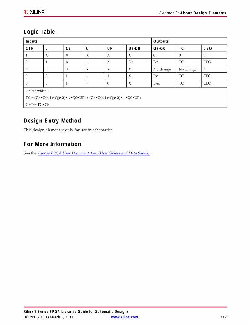
Chapter 3: About Design Elements
Logic TableInputs Outputs
CLR L CE C UP Dz-D0 Qz-Q0 TC CEO1 X X X X X 0 0 0
0 1 X ↑ X Dn Dn TC CEO
0 0 0 X X X No change No change 0
0 0 1 ↑ 1 X Inc TC CEO
0 0 1 ↑ 0 X Dec TC CEO
z = bit width - 1
TC = (Qz•Q(z-1)•Q(z-2)•...•Q0•UP) + (Qz•Q(z-1)•Q(z-2)•...•Q0•UP)
CEO = TC•CE
Design Entry MethodThis design element is only for use in schematics.
For More InformationSee the 7 series FPGA User Documentation (User Guides and Data Sheets).
Xilinx 7 Series FPGA Libraries Guide for Schematic DesignsUG799 (v 13.1) March 1, 2011 www.xilinx.com 107

Chapter 3: About Design Elements
CB8REMacro: 8-Bit Cascadable Binary Counter with Clock Enable and Synchronous Reset
IntroductionThis design element is a synchronous, resettable, cascadable binary counter. The synchronous reset (R), whenHigh, overrides all other inputs and forces the Q outputs, terminal count (TC), and clock enable out (CEO) tozero on the Low-to-High clock transition. The Q outputs increment when the clock enable input (CE) is Highduring the Low-to-High clock (C) transition. The counter ignores clock transitions when CE is Low. The TCoutput is High when both Q outputs are High.
Create larger counters by connecting the CEO output of each stage to the CE input of the next stage andconnecting the C and R inputs in parallel. CEO is active (High) when TC and CE are High. The maximum lengthof the counter is determined by the accumulated CE-to-TC propagation delays versus the clock period. Theclock period must be greater than n (tCE-TC), where n is the number of stages and the time tCE-TC is the CE-to-TCpropagation delay of each stage. When cascading counters, use the CEO output if the counter uses the CEinput or use the TC output if it does not.
This counter is asynchronously cleared, outputs Low, when power is applied. For FPGA devices, power-onconditions are simulated when global set/reset (GSR) is active. GSR defaults to active-High but can be invertedby adding an inverter in front of the GSR input of the appropriate STARTUP_architecture symbol.
Logic TableInputs Outputs
R CE C Qz-Q0 TC CEO1 X ↑ 0 0 0
0 0 X No change No change 0
0 1 ↑ Inc TC CEO
z = bit width - 1
TC = Qz•Q(z-1)•Q(z-2)•...•Q0)
CEO = TC•CE
Design Entry MethodThis design element is only for use in schematics.
For More InformationSee the 7 series FPGA User Documentation (User Guides and Data Sheets).
Xilinx 7 Series FPGA Libraries Guide for Schematic Designs108 www.xilinx.com UG799 (v 13.1) March 1, 2011

Chapter 3: About Design Elements
CC16CEMacro: 16-Bit Cascadable Binary Counter with Clock Enable and Asynchronous Clear
IntroductionThis design element is an asynchronously clearable, cascadable binary counter. It is implemented using carrylogic with relative location constraints to ensure efficient logic placement. The asynchronous clear (CLR) is thehighest priority input. When CLR is High, all other inputs are ignored; the Q outputs, terminal count (TC), andclock enable out (CEO) go to logic level zero, independent of clock transitions. The Q outputs increment whenthe clock enable input (CE) is High during the Low-to-High clock (C) transition. The counter ignores clocktransitions when CE is Low. The TC output is High when all Q outputs are High.
Create larger counters by connecting the CEO output of each stage to the CE input of the next stage andconnecting the C and CLR inputs in parallel. CEO is active (High) when TC and CE are High. The maximumlength of the counter is determined by the accumulated CE-to-TC propagation delays versus the clock period.The clock period must be greater than n (tCE-TC), where n is the number of stages and the time tCE-TC is theCE-to-TC propagation delay of each stage. When cascading counters, use the CEO output if the counter uses theCE input or use the TC output if it does not.
This counter is asynchronously cleared, outputs Low, when power is applied. For FPGA devices, power-onconditions are simulated when global set/reset (GSR) is active. GSR defaults to active-High but can be invertedby adding an inverter in front of the GSR input of the appropriate STARTUP_architecture symbol.
Logic TableInputs Outputs
CLR CE C Qz-Q0 TC CEO1 X X 0 0 0
0 0 X No change No change 0
0 1 ↑ Inc TC CEO
z = bit width - 1
TC = Qz•Q(z-1)•Q(z-2)•...•Q0
CEO = TC•CE
Design Entry MethodThis design element is only for use in schematics.
For More InformationSee the 7 series FPGA User Documentation (User Guides and Data Sheets).
Xilinx 7 Series FPGA Libraries Guide for Schematic DesignsUG799 (v 13.1) March 1, 2011 www.xilinx.com 109

Chapter 3: About Design Elements
CC16CLEMacro: 16-Bit Loadable Cascadable Binary Counter with Clock Enable and AsynchronousClear
IntroductionThis design element is a synchronously loadable, asynchronously clearable, cascadable binary counter. It isimplemented using carry logic with relative location constraints to ensure efficient logic placement. Theasynchronous clear (CLR) is the highest priority input. When CLR is High, all other inputs are ignored;the Q outputs, terminal count (TC), and clock enable out (CEO) go to logic level zero, independent of clocktransitions. The data on the D inputs is loaded into the counter when the load enable input (L) is High during theLow-to-High clock (C) transition, independent of the state of clock enable (CE). The Q outputs increment whenCE is High during the Low-to-High clock transition. The counter ignores clock transitions when CE is Low.The TC output is High when all Q outputs are High.
Create larger counters by connecting the CEO output of each stage to the CE input of the next stage andconnecting the C, L, and CLR inputs in parallel. CEO is active (High) when TC and CE are High. The maximumlength of the counter is determined by the accumulated CE-to-TC propagation delays versus the clock period.The clock period must be greater than n (tCE-TC), where n is the number of stages and the time tCE-TC is theCE-to-TC propagation delay of each stage. When cascading counters, use the CEO output if the counter uses theCE input or use the TC output if it does not.
This counter is asynchronously cleared, outputs Low, when power is applied. For FPGA devices, power-onconditions are simulated when global set/reset (GSR) is active. GSR defaults to active-High but can be invertedby adding an inverter in front of the GSR input of the appropriate STARTUP_architecture symbol.
Logic TableInputs Outputs
CLR L CE C Dz-D0 Qz-Q0 TC CEO1 X X X X 0 0 0
0 1 X ↑ Dn Dn TC CEO
0 0 0 X X No change No change 0
0 0 1 ↑ X Inc TC CEO
z = bit width - 1
TC = Qz•Q(z-1)•Q(z-2)•...•Q0
CEO = TC•CE
Design Entry MethodThis design element is only for use in schematics.
Xilinx 7 Series FPGA Libraries Guide for Schematic Designs110 www.xilinx.com UG799 (v 13.1) March 1, 2011

Chapter 3: About Design Elements
For More InformationSee the 7 series FPGA User Documentation (User Guides and Data Sheets).
Xilinx 7 Series FPGA Libraries Guide for Schematic DesignsUG799 (v 13.1) March 1, 2011 www.xilinx.com 111

Chapter 3: About Design Elements
CC16CLEDMacro: 16-Bit Loadable Cascadable Bidirectional Binary Counter with Clock Enable andAsynchronous Clear
IntroductionThis design element is a synchronously loadable, asynchronously clearable, cascadable, bidirectional binarycounter. It is implemented using carry logic with relative location constraints, which assures most efficient logicplacement. The asynchronous clear (CLR) is the highest priority input. When CLR is High, all other inputs areignored; the Q outputs, terminal count (TC), and clock enable out (CEO) go to logic level zero, independent ofclock transitions. The data on the D inputs is loaded into the counter when the load enable input (L) is Highduring the Low-to-High clock (C) transition, independent of the state of clock enable (CE). The Q outputsdecrement when CE is High and UP is Low during the Low-to-High clock transition. The Q outputs incrementwhen CE and UP are High. The counter ignores clock transitions when CE is Low.
For counting up, the TC output is High when all Q outputs and UP are High. For counting down, the TCoutput is High when all Q outputs and UP are Low.
Create larger counters by connecting the CEO output of each stage to the CE input of the next stage andconnecting the C, UP, L, and CLR inputs in parallel. CEO is active (High) when TC and CE are High. Themaximum length of the counter is determined by the accumulated CE-to-TC propagation delays versus the clockperiod. The clock period must be greater than n (tCE-TC), where n is the number of stages and the time tCE-TC isthe CE-to-TC propagation delay of each stage. When cascading counters, use the CEO output if the counteruses the CE input or use the TC output if it does not.
This counter is asynchronously cleared, outputs Low, when power is applied. For FPGA devices, power-onconditions are simulated when global set/reset (GSR) is active. GSR defaults to active-High but can be invertedby adding an inverter in front of the GSR input of the appropriate STARTUP_architecture symbol.
Xilinx 7 Series FPGA Libraries Guide for Schematic Designs112 www.xilinx.com UG799 (v 13.1) March 1, 2011

Chapter 3: About Design Elements
Logic TableInputs Outputs
CLR L CE C UP Dz-D0 Qz-Q0 TC CEO1 X X X X X 0 0 0
0 1 X ↑ X Dn Dn TC CEO
0 0 0 X X X No change No change 0
0 0 1 ↑ 1 X Inc TC CEO
0 0 1 ↑ 0 X Dec TC CEO
z = bit width - 1
TC = (Qz•Q(z-1)•Q(z-2)•...•Q0•UP) + (Qz•Q(z-1)•Q(z-2)•...•Q0•UP)
CEO = TC•CE
Design Entry MethodThis design element is only for use in schematics.
For More InformationSee the 7 series FPGA User Documentation (User Guides and Data Sheets).
Xilinx 7 Series FPGA Libraries Guide for Schematic DesignsUG799 (v 13.1) March 1, 2011 www.xilinx.com 113
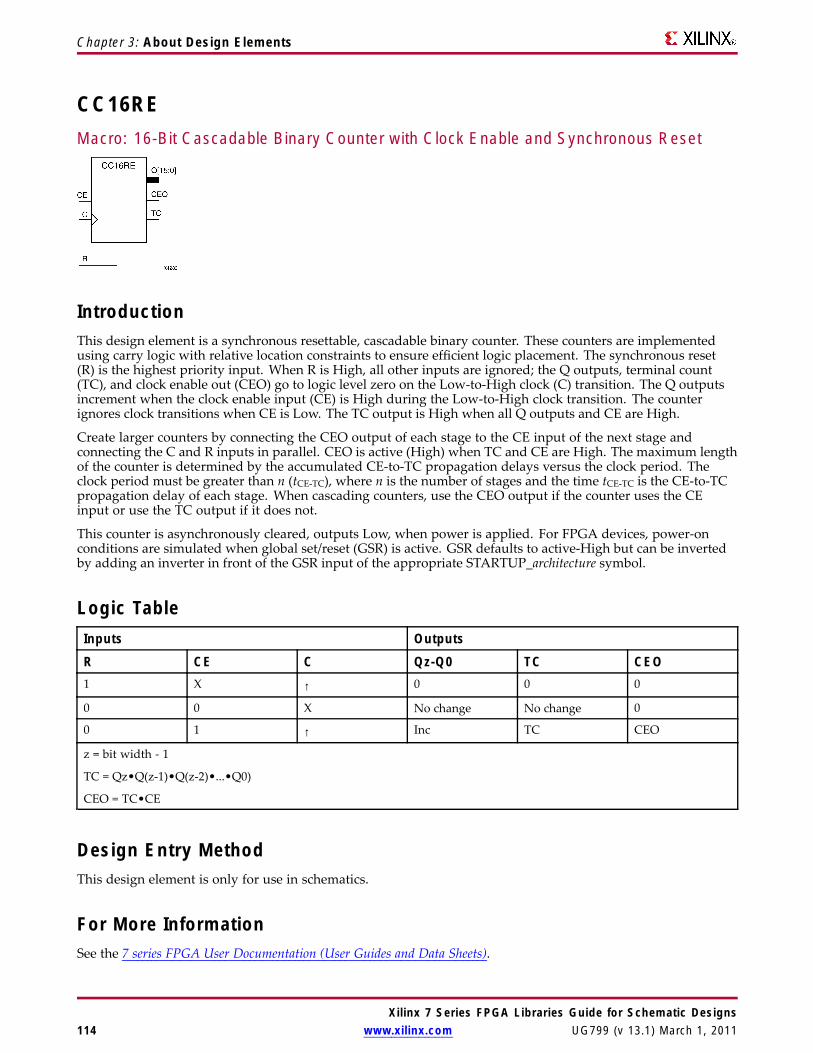
Chapter 3: About Design Elements
CC16REMacro: 16-Bit Cascadable Binary Counter with Clock Enable and Synchronous Reset
IntroductionThis design element is a synchronous resettable, cascadable binary counter. These counters are implementedusing carry logic with relative location constraints to ensure efficient logic placement. The synchronous reset(R) is the highest priority input. When R is High, all other inputs are ignored; the Q outputs, terminal count(TC), and clock enable out (CEO) go to logic level zero on the Low-to-High clock (C) transition. The Q outputsincrement when the clock enable input (CE) is High during the Low-to-High clock transition. The counterignores clock transitions when CE is Low. The TC output is High when all Q outputs and CE are High.
Create larger counters by connecting the CEO output of each stage to the CE input of the next stage andconnecting the C and R inputs in parallel. CEO is active (High) when TC and CE are High. The maximum lengthof the counter is determined by the accumulated CE-to-TC propagation delays versus the clock period. Theclock period must be greater than n (tCE-TC), where n is the number of stages and the time tCE-TC is the CE-to-TCpropagation delay of each stage. When cascading counters, use the CEO output if the counter uses the CEinput or use the TC output if it does not.
This counter is asynchronously cleared, outputs Low, when power is applied. For FPGA devices, power-onconditions are simulated when global set/reset (GSR) is active. GSR defaults to active-High but can be invertedby adding an inverter in front of the GSR input of the appropriate STARTUP_architecture symbol.
Logic TableInputs Outputs
R CE C Qz-Q0 TC CEO1 X ↑ 0 0 0
0 0 X No change No change 0
0 1 ↑ Inc TC CEO
z = bit width - 1
TC = Qz•Q(z-1)•Q(z-2)•...•Q0)
CEO = TC•CE
Design Entry MethodThis design element is only for use in schematics.
For More InformationSee the 7 series FPGA User Documentation (User Guides and Data Sheets).
Xilinx 7 Series FPGA Libraries Guide for Schematic Designs114 www.xilinx.com UG799 (v 13.1) March 1, 2011

Chapter 3: About Design Elements
CC8CEMacro: 8-Bit Cascadable Binary Counter with Clock Enable and Asynchronous Clear
IntroductionThis design element is an asynchronously clearable, cascadable binary counter. It is implemented using carrylogic with relative location constraints to ensure efficient logic placement. The asynchronous clear (CLR) is thehighest priority input. When CLR is High, all other inputs are ignored; the Q outputs, terminal count (TC), andclock enable out (CEO) go to logic level zero, independent of clock transitions. The Q outputs increment whenthe clock enable input (CE) is High during the Low-to-High clock (C) transition. The counter ignores clocktransitions when CE is Low. The TC output is High when all Q outputs are High.
Create larger counters by connecting the CEO output of each stage to the CE input of the next stage andconnecting the C and CLR inputs in parallel. CEO is active (High) when TC and CE are High. The maximumlength of the counter is determined by the accumulated CE-to-TC propagation delays versus the clock period.The clock period must be greater than n (tCE-TC), where n is the number of stages and the time tCE-TC is theCE-to-TC propagation delay of each stage. When cascading counters, use the CEO output if the counter uses theCE input or use the TC output if it does not.
This counter is asynchronously cleared, outputs Low, when power is applied. For FPGA devices, power-onconditions are simulated when global set/reset (GSR) is active. GSR defaults to active-High but can be invertedby adding an inverter in front of the GSR input of the appropriate STARTUP_architecture symbol.
Logic TableInputs Outputs
CLR CE C Qz-Q0 TC CEO1 X X 0 0 0
0 0 X No change No change 0
0 1 ↑ Inc TC CEO
z = bit width - 1
TC = Qz•Q(z-1)•Q(z-2)•...•Q0
CEO = TC•CE
Design Entry MethodThis design element is only for use in schematics.
For More InformationSee the 7 series FPGA User Documentation (User Guides and Data Sheets).
Xilinx 7 Series FPGA Libraries Guide for Schematic DesignsUG799 (v 13.1) March 1, 2011 www.xilinx.com 115

Chapter 3: About Design Elements
CC8CLEMacro: 8-Bit Loadable Cascadable Binary Counter with Clock Enable and AsynchronousClear
IntroductionThis design element is a synchronously loadable, asynchronously clearable, cascadable binary counter. It isimplemented using carry logic with relative location constraints to ensure efficient logic placement. Theasynchronous clear (CLR) is the highest priority input. When CLR is High, all other inputs are ignored;the Q outputs, terminal count (TC), and clock enable out (CEO) go to logic level zero, independent of clocktransitions. The data on the D inputs is loaded into the counter when the load enable input (L) is High during theLow-to-High clock (C) transition, independent of the state of clock enable (CE). The Q outputs increment whenCE is High during the Low-to-High clock transition. The counter ignores clock transitions when CE is Low.The TC output is High when all Q outputs are High.
Create larger counters by connecting the CEO output of each stage to the CE input of the next stage andconnecting the C, L, and CLR inputs in parallel. CEO is active (High) when TC and CE are High. The maximumlength of the counter is determined by the accumulated CE-to-TC propagation delays versus the clock period.The clock period must be greater than n (tCE-TC), where n is the number of stages and the time tCE-TC is theCE-to-TC propagation delay of each stage. When cascading counters, use the CEO output if the counter uses theCE input or use the TC output if it does not.
This counter is asynchronously cleared, outputs Low, when power is applied. For FPGA devices, power-onconditions are simulated when global set/reset (GSR) is active. GSR defaults to active-High but can be invertedby adding an inverter in front of the GSR input of the appropriate STARTUP_architecture symbol.
Logic TableInputs Outputs
CLR L CE C Dz-D0 Qz-Q0 TC CEO1 X X X X 0 0 0
0 1 X ↑ Dn Dn TC CEO
0 0 0 X X No change No change 0
0 0 1 ↑ X Inc TC CEO
z = bit width - 1
TC = Qz•Q(z-1)•Q(z-2)•...•Q0
CEO = TC•CE
Design Entry MethodThis design element is only for use in schematics.
Xilinx 7 Series FPGA Libraries Guide for Schematic Designs116 www.xilinx.com UG799 (v 13.1) March 1, 2011

Chapter 3: About Design Elements
For More InformationSee the 7 series FPGA User Documentation (User Guides and Data Sheets).
Xilinx 7 Series FPGA Libraries Guide for Schematic DesignsUG799 (v 13.1) March 1, 2011 www.xilinx.com 117

Chapter 3: About Design Elements
CC8CLEDMacro: 8-Bit Loadable Cascadable Bidirectional Binary Counter with Clock Enable andAsynchronous Clear
IntroductionThis design element is a synchronously loadable, asynchronously clearable, cascadable, bidirectional binarycounter. It is implemented using carry logic with relative location constraints, which assures most efficient logicplacement. The asynchronous clear (CLR) is the highest priority input. When CLR is High, all other inputs areignored; the Q outputs, terminal count (TC), and clock enable out (CEO) go to logic level zero, independent ofclock transitions. The data on the D inputs is loaded into the counter when the load enable input (L) is Highduring the Low-to-High clock (C) transition, independent of the state of clock enable (CE). The Q outputsdecrement when CE is High and UP is Low during the Low-to-High clock transition. The Q outputs incrementwhen CE and UP are High. The counter ignores clock transitions when CE is Low.
For counting up, the TC output is High when all Q outputs and UP are High. For counting down, the TCoutput is High when all Q outputs and UP are Low.
Create larger counters by connecting the CEO output of each stage to the CE input of the next stage andconnecting the C, UP, L, and CLR inputs in parallel. CEO is active (High) when TC and CE are High. Themaximum length of the counter is determined by the accumulated CE-to-TC propagation delays versus the clockperiod. The clock period must be greater than n (tCE-TC), where n is the number of stages and the time tCE-TC isthe CE-to-TC propagation delay of each stage. When cascading counters, use the CEO output if the counteruses the CE input or use the TC output if it does not.
This counter is asynchronously cleared, outputs Low, when power is applied. For FPGA devices, power-onconditions are simulated when global set/reset (GSR) is active. GSR defaults to active-High but can be invertedby adding an inverter in front of the GSR input of the appropriate STARTUP_architecture symbol.
Xilinx 7 Series FPGA Libraries Guide for Schematic Designs118 www.xilinx.com UG799 (v 13.1) March 1, 2011

Chapter 3: About Design Elements
Logic TableInputs Outputs
CLR L CE C UP Dz-D0 Qz-Q0 TC CEO1 X X X X X 0 0 0
0 1 X ↑ X Dn Dn TC CEO
0 0 0 X X X No change No change 0
0 0 1 ↑ 1 X Inc TC CEO
0 0 1 ↑ 0 X Dec TC CEO
z = bit width - 1
TC = (Qz•Q(z-1)•Q(z-2)•...•Q0•UP) + (Qz•Q(z-1)•Q(z-2)•...•Q0•UP)
CEO = TC•CE
Design Entry MethodThis design element is only for use in schematics.
For More InformationSee the 7 series FPGA User Documentation (User Guides and Data Sheets).
Xilinx 7 Series FPGA Libraries Guide for Schematic DesignsUG799 (v 13.1) March 1, 2011 www.xilinx.com 119

Chapter 3: About Design Elements
CC8REMacro: 8-Bit Cascadable Binary Counter with Clock Enable and Synchronous Reset
IntroductionThis design element is a synchronous resettable, cascadable binary counter. These counters are implementedusing carry logic with relative location constraints to ensure efficient logic placement. The synchronous reset(R) is the highest priority input. When R is High, all other inputs are ignored; the Q outputs, terminal count(TC), and clock enable out (CEO) go to logic level zero on the Low-to-High clock (C) transition. The Q outputsincrement when the clock enable input (CE) is High during the Low-to-High clock transition. The counterignores clock transitions when CE is Low. The TC output is High when all Q outputs and CE are High.
Create larger counters by connecting the CEO output of each stage to the CE input of the next stage andconnecting the C and R inputs in parallel. CEO is active (High) when TC and CE are High. The maximum lengthof the counter is determined by the accumulated CE-to-TC propagation delays versus the clock period. Theclock period must be greater than n (tCE-TC), where n is the number of stages and the time tCE-TC is the CE-to-TCpropagation delay of each stage. When cascading counters, use the CEO output if the counter uses the CEinput or use the TC output if it does not.
This counter is asynchronously cleared, outputs Low, when power is applied. For FPGA devices, power-onconditions are simulated when global set/reset (GSR) is active. GSR defaults to active-High but can be invertedby adding an inverter in front of the GSR input of the appropriate STARTUP_architecture symbol.
Logic TableInputs Outputs
R CE C Qz-Q0 TC CEO1 X ↑ 0 0 0
0 0 X No change No change 0
0 1 ↑ Inc TC CEO
z = bit width - 1
TC = Qz•Q(z-1)•Q(z-2)•...•Q0)
CEO = TC•CE
Design Entry MethodThis design element is only for use in schematics.
For More InformationSee the 7 series FPGA User Documentation (User Guides and Data Sheets).
Xilinx 7 Series FPGA Libraries Guide for Schematic Designs120 www.xilinx.com UG799 (v 13.1) March 1, 2011
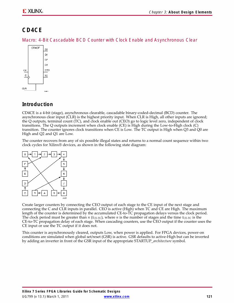
Chapter 3: About Design Elements
CD4CEMacro: 4-Bit Cascadable BCD Counter with Clock Enable and Asynchronous Clear
IntroductionCD4CE is a 4-bit (stage), asynchronous clearable, cascadable binary-coded-decimal (BCD) counter. Theasynchronous clear input (CLR) is the highest priority input. When CLR is High, all other inputs are ignored;the Q outputs, terminal count (TC), and clock enable out (CEO) go to logic level zero, independent of clocktransitions. The Q outputs increment when clock enable (CE) is High during the Low-to-High clock (C)transition. The counter ignores clock transitions when CE is Low. The TC output is High when Q3 and Q0 areHigh and Q2 and Q1 are Low.
The counter recovers from any of six possible illegal states and returns to a normal count sequence within twoclock cycles for Xilinx® devices, as shown in the following state diagram:
Create larger counters by connecting the CEO output of each stage to the CE input of the next stage andconnecting the C and CLR inputs in parallel. CEO is active (High) when TC and CE are High. The maximumlength of the counter is determined by the accumulated CE-to-TC propagation delays versus the clock period.The clock period must be greater than n (tCE-TC), where n is the number of stages and the time tCE-TC is theCE-to-TC propagation delay of each stage. When cascading counters, use the CEO output if the counter uses theCE input or use the TC output if it does not.
This counter is asynchronously cleared, outputs Low, when power is applied. For FPGA devices, power-onconditions are simulated when global set/reset (GSR) is active. GSR defaults to active-High but can be invertedby adding an inverter in front of the GSR input of the appropriate STARTUP_architecture symbol.
Xilinx 7 Series FPGA Libraries Guide for Schematic DesignsUG799 (v 13.1) March 1, 2011 www.xilinx.com 121

Chapter 3: About Design Elements
Logic TableInputs Outputs
CLR CE C Q3 Q2 Q1 Q0 TC CEO1 X X 0 0 0 0 0 0
0 1 ↑ Inc Inc Inc Inc TC CEO
0 0 X No Change No Change No Change No Change TC 0
0 1 X 1 0 0 1 1 1
TC = Q3•!Q2•!Q1•Q0
CEO = TC•CE
Design Entry MethodThis design element is only for use in schematics.
For More InformationSee the 7 series FPGA User Documentation (User Guides and Data Sheets).
Xilinx 7 Series FPGA Libraries Guide for Schematic Designs122 www.xilinx.com UG799 (v 13.1) March 1, 2011

Chapter 3: About Design Elements
CD4CLEMacro: 4-Bit Loadable Cascadable BCD Counter with Clock Enable and AsynchronousClear
IntroductionCD4CLE is a 4-bit (stage), synchronously loadable, asynchronously clearable, binarycoded- decimal (BCD)counter. The asynchronous clear input (CLR) is the highest priority input. When (CLR) is High, all other inputsare ignored; the (Q) outputs, terminal count (TC), and clock enable out (CEO) go to logic level zero, independentof clock transitions. The data on the (D) inputs is loaded into the counter when the load enable input (L) is Highduring the Low-to-High clock (C) transition. The (Q) outputs increment when clock enable input (CE) is Highduring the Low- to-High clock transition. The counter ignores clock transitions when (CE) is Low. The (TC)output is High when Q3 and Q0 are High and Q2 and Q1 are Low.
The counter recovers from any of six possible illegal states and returns to a normal count sequence within twoclock cycles for Xilinx® devices, as shown in the following state diagram:
Create larger counters by connecting the CEO output of each stage to the CE input of the next stage andconnecting the C, L, and CLR inputs in parallel. CEO is active (High) when TC and CE are High. The maximumlength of the counter is determined by the accumulated CE-to-TC propagation delays versus the clock period.The clock period must be greater than n (tCE-TC), where n is the number of stages and the time tCE-TC is theCE-to-TC propagation delay of each stage. When cascading counters, use the CEO output if the counter uses theCE input or use the TC output if it does not.
This counter is asynchronously cleared, outputs Low, when power is applied. For FPGA devices, power-onconditions are simulated when global set/reset (GSR) is active. GSR defaults to active-High but can be invertedby adding an inverter in front of the GSR input of the appropriate STARTUP_architecture symbol.
Xilinx 7 Series FPGA Libraries Guide for Schematic DesignsUG799 (v 13.1) March 1, 2011 www.xilinx.com 123

Chapter 3: About Design Elements
Logic TableInputs Outputs
CLR L CE D3 : D0 C Q3 Q2 Q1 Q0 TC CEO1 X X X X 0 0 0 0 0 0
0 1 X D3 : D0 ↑ D3 D2 D1 D0 TC CEO
0 0 1 X ↑ Inc Inc Inc Inc TC CEO
0 0 0 X X NoChange
NoChange
NoChange
NoChange
TC 0
0 0 1 X X 1 0 0 1 1 1
TC = Q3•!Q2•!Q1•Q0
CEO = TC•CE
Design Entry MethodThis design element is only for use in schematics.
For More InformationSee the 7 series FPGA User Documentation (User Guides and Data Sheets).
Xilinx 7 Series FPGA Libraries Guide for Schematic Designs124 www.xilinx.com UG799 (v 13.1) March 1, 2011
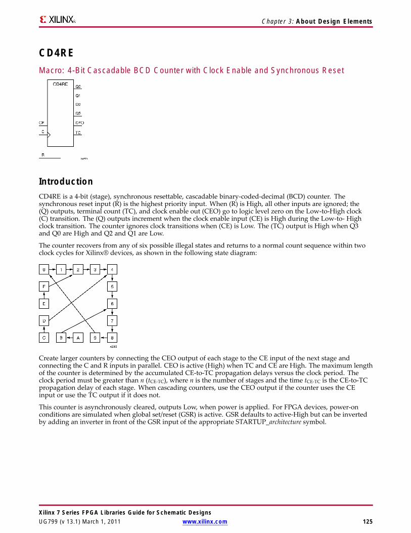
Chapter 3: About Design Elements
CD4REMacro: 4-Bit Cascadable BCD Counter with Clock Enable and Synchronous Reset
IntroductionCD4RE is a 4-bit (stage), synchronous resettable, cascadable binary-coded-decimal (BCD) counter. Thesynchronous reset input (R) is the highest priority input. When (R) is High, all other inputs are ignored; the(Q) outputs, terminal count (TC), and clock enable out (CEO) go to logic level zero on the Low-to-High clock(C) transition. The (Q) outputs increment when the clock enable input (CE) is High during the Low-to- Highclock transition. The counter ignores clock transitions when (CE) is Low. The (TC) output is High when Q3and Q0 are High and Q2 and Q1 are Low.
The counter recovers from any of six possible illegal states and returns to a normal count sequence within twoclock cycles for Xilinx® devices, as shown in the following state diagram:
Create larger counters by connecting the CEO output of each stage to the CE input of the next stage andconnecting the C and R inputs in parallel. CEO is active (High) when TC and CE are High. The maximum lengthof the counter is determined by the accumulated CE-to-TC propagation delays versus the clock period. Theclock period must be greater than n (tCE-TC), where n is the number of stages and the time tCE-TC is the CE-to-TCpropagation delay of each stage. When cascading counters, use the CEO output if the counter uses the CEinput or use the TC output if it does not.
This counter is asynchronously cleared, outputs Low, when power is applied. For FPGA devices, power-onconditions are simulated when global set/reset (GSR) is active. GSR defaults to active-High but can be invertedby adding an inverter in front of the GSR input of the appropriate STARTUP_architecture symbol.
Xilinx 7 Series FPGA Libraries Guide for Schematic DesignsUG799 (v 13.1) March 1, 2011 www.xilinx.com 125

Chapter 3: About Design Elements
Logic TableInputs Outputs
R CE C Q3 Q2 Q1 Q0 TC CEO1 X ↑ 0 0 0 0 0 0
0 1 ↑ Inc Inc Inc Inc TC CEO
0 0 X No Change No Change No Change No Change TC 0
0 1 X 1 0 0 1 1 1
TC = Q3•!Q2•!Q1•Q0
CEO = TC•CE
Design Entry MethodThis design element is only for use in schematics.
For More InformationSee the 7 series FPGA User Documentation (User Guides and Data Sheets).
Xilinx 7 Series FPGA Libraries Guide for Schematic Designs126 www.xilinx.com UG799 (v 13.1) March 1, 2011

Chapter 3: About Design Elements
CD4RLEMacro: 4-Bit Loadable Cascadable BCD Counter with Clock Enable and SynchronousReset
IntroductionCD4RLE is a 4-bit (stage), synchronous loadable, resettable, binary-coded-decimal (BCD) counter. Thesynchronous reset input (R) is the highest priority input. When R is High, all other inputs are ignored; theQ outputs, terminal count (TC), and clock enable out (CEO) go to logic level zero on the Low-to-High clocktransitions. The data on the D inputs is loaded into the counter when the load enable input (L) is High during theLow-to-High clock (C) transition. The Q outputs increment when the clock enable input (CE) is High during theLow-to-High clock transition. The counter ignores clock transitions when CE is Low. The TC output is Highwhen Q3 and Q0 are High and Q2 and Q1 are Low.
The counter recovers from any of six possible illegal states and returns to a normal count sequence within twoclock cycles for Xilinx® devices, as shown in the following state diagram:
Create larger counters by connecting the CEO output of each stage to the CE input of the next stage andconnecting the C, L, and R inputs in parallel. CEO is active (High) when TC and CE are High. The maximumlength of the counter is determined by the accumulated CE-to-TC propagation delays versus the clock period.The clock period must be greater than n (tCE-TC), where n is the number of stages and the time tCE-TC is theCE-to-TC propagation delay of each stage. When cascading counters, use the CEO output if the counter uses theCE input or use the TC output if it does not.
This counter is asynchronously cleared, outputs Low, when power is applied. For FPGA devices, power-onconditions are simulated when global set/reset (GSR) is active. GSR defaults to active-High but can be invertedby adding an inverter in front of the GSR input of the appropriate STARTUP_architecture symbol.
Xilinx 7 Series FPGA Libraries Guide for Schematic DesignsUG799 (v 13.1) March 1, 2011 www.xilinx.com 127

Chapter 3: About Design Elements
Logic TableInputs Outputs
R L CE D3 : D0 C Q3 Q2 Q1 Q0 TC CEO1 X X X ↑ 0 0 0 0 0 0
0 1 X D3 : D0 ↑ D3 D D D0 TC CEO
0 0 1 X ↑ Inc Inc Inc Inc TC CEO
0 0 0 X X NoChange
NoChange
NoChange
NoChange
TC 0
0 0 1 X X 1 0 0 1 1 1
TC = Q3•!Q2•!Q1•Q0
CEO = TC•CE
Design Entry MethodThis design element is only for use in schematics.
For More InformationSee the 7 series FPGA User Documentation (User Guides and Data Sheets).
Xilinx 7 Series FPGA Libraries Guide for Schematic Designs128 www.xilinx.com UG799 (v 13.1) March 1, 2011

Chapter 3: About Design Elements
CFGLUT5Primitive: 5-input Dynamically Reconfigurable Look-Up Table (LUT)
IntroductionThis element is a runtime, dynamically reconfigurable, 5-input look-up table (LUT) that enables the changingof the logical function of the LUT during circuit operation. Using the CDI pin, a new INIT value can besynchronously shifted in serially to change the logical function. The O6 output pin produces the logical outputfunction, based on the current INIT value loaded into the LUT and the currently selected I0-I4 input pins.Optionally, you can use the O5 output in combination with the O6 output to create two individual 4-inputfunctions sharing the same inputs or a 5-input function and a 4-input function that uses a subset of the 5-inputlogic (see tables below). This component occupies one of the four 6-LUT components within a slice.
To cascade this element, connect the CDO pin from each element to the CDI input of the next element. This willallow a single serial chain of data (32-bits per LUT) to reconfigure multiple LUTs.
Port DescriptionsPort Direction Width FunctionO6 Output 1 5-LUT output
O5 Output 1 4-LUT output
I0, I1, I2, I3, I4 Input 1 LUT inputs
CDO Output 1 Reconfiguration data cascaded output (optionally connect to the CDI inputof a subsequent LUT)
CDI Input 1 Reconfiguration data serial input
CLK Input 1 Reconfiguration clock
CE Input 1 Active high reconfiguration clock enable
Design Entry MethodThis design element can be used in schematics.• Connect the CLK input to the clock source used to supply the reconfiguration data.• Connect the CDI input to the source of the reconfiguration data.• Connect the CE pin to the active high logic if you need to enable/disable LUT reconfiguration.• Connect the I4-I0 pins to the source inputs to the logic equation. The logic function is output on O6 and O5.• To cascade this element, connect the CDO pin from each element to the CDI input of the next element to
allow a single serial chain of data to reconfigure multiple LUTs.
The INIT attribute should be placed on this design element to specify the initial logical function of the LUT. Anew INIT can be loaded into the LUT any time during circuit operation by shifting in 32-bits per LUT in thechain, representing the new INIT value. Disregard the O6 and O5 output data until all 32-bits of new INIT datahas been clocked into the LUT. The logical function of the LUT changes as new INIT data is shifted into it. Datashould be shifted in MSB (INIT[31]) first and LSB (INIT[0]) last.
Xilinx 7 Series FPGA Libraries Guide for Schematic DesignsUG799 (v 13.1) March 1, 2011 www.xilinx.com 129

Chapter 3: About Design Elements
In order to understand the O6 and O5 logical value based on the current INIT, see the table below:
I4 I3 I2 I1 I0 O6 Value O5 Value1 1 1 1 1 INIT[31] INIT[15]
1 1 1 1 0 INIT[30] INIT[14]. . . . . . . . .
1 0 0 0 1 INIT[17] INIT[1]
1 0 0 0 0 INIT[16] INIT[0]
0 1 1 1 1 INIT[15] INIT[15]
0 1 1 1 0 INIT[14] INIT[14]. . . . . . . . .
0 0 0 0 1 INIT[1] INIT[1]
0 0 0 0 0 INIT[0] INIT[0]
For instance, the INIT value of FFFF8000 would represent the following logical equations:
• O6 = I4 or (I3 and I2 and I1 and I0)
• O5 = I3 and I2 and I1 and I0
To use these elements as two, 4-input LUTs with the same inputs but different functions, tie the I4 signal to alogical one. The INIT[31:16] values apply to the logical values of the O6 output and INIT [15:0] apply to thelogical values of the O5 output.
Available AttributesAttribute Type Allowed Values Default DescriptionINIT Hexadecimal Any 32-bit Value All zeros Specifies the initial logical expression of
this element.
For More InformationSee the 7 series FPGA User Documentation (User Guides and Data Sheets).
Xilinx 7 Series FPGA Libraries Guide for Schematic Designs130 www.xilinx.com UG799 (v 13.1) March 1, 2011

Chapter 3: About Design Elements
CJ4CEMacro: 4-Bit Johnson Counter with Clock Enable and Asynchronous Clear
IntroductionThis design element is a clearable Johnson/shift counter. The asynchronous clear (CLR) input, when High,overrides all other inputs and forces the data (Q) outputs to logic level zero, independent of clock (C) transitions.The counter increments (shifts Q0 to Q1, Q1 to Q2,and so forth) when the clock enable input (CE) is High duringthe Low-to-High clock transition. Clock transitions are ignored when (CE) is Low.
The Q3 output is inverted and fed back to input Q0 to provide continuous counting operation.
This counter is asynchronously cleared, outputs Low, when power is applied. For FPGA devices, power-onconditions are simulated when global set/reset (GSR) is active. GSR defaults to active-High but can be invertedby adding an inverter in front of the GSR input of the appropriate STARTUP_architecture symbol.
Logic TableInputs Outputs
CLR CE C Q0 Q1 through Q31 X X 0 0
0 0 X No change No change
0 1 ↑ !q3 q0 through q2
q = state of referenced output one setup time prior to active clock transition
Design Entry MethodThis design element is only for use in schematics.
For More InformationSee the 7 series FPGA User Documentation (User Guides and Data Sheets).
Xilinx 7 Series FPGA Libraries Guide for Schematic DesignsUG799 (v 13.1) March 1, 2011 www.xilinx.com 131

Chapter 3: About Design Elements
CJ4REMacro: 4-Bit Johnson Counter with Clock Enable and Synchronous Reset
IntroductionThis design element is a resettable Johnson/shift counter. The synchronous reset (R) input, when High, overridesall other inputs and forces the data (Q) outputs to logic level zero during the Low-to-High clock (C) transition.The counter increments (shifts Q0 to Q1, Q1 to Q2, and so forth) when the clock enable input (CE) is High duringthe Low-to-High clock transition. Clock transitions are ignored when CE is Low.
The Q3 output is inverted and fed back to input Q0 to provide continuous counting operation.
This counter is asynchronously cleared, outputs Low, when power is applied. For FPGA devices, power-onconditions are simulated when global set/reset (GSR) is active. GSR defaults to active-High but can be invertedby adding an inverter in front of the GSR input of the appropriate STARTUP_architecture symbol.
Logic TableInputs Outputs
R CE C Q0 Q1 through Q31 X ↑ 0 0
0 0 X No change No change
0 1 ↑ !q3 q0 through q2
q = state of referenced output one setup time prior to active clock transition
Design Entry MethodThis design element is only for use in schematics.
For More InformationSee the 7 series FPGA User Documentation (User Guides and Data Sheets).
Xilinx 7 Series FPGA Libraries Guide for Schematic Designs132 www.xilinx.com UG799 (v 13.1) March 1, 2011

Chapter 3: About Design Elements
CJ5CEMacro: 5-Bit Johnson Counter with Clock Enable and Asynchronous Clear
IntroductionThis design element is a clearable Johnson/shift counter. The asynchronous clear (CLR) input, when High,overrides all other inputs and forces the data (Q) outputs to logic level zero, independent of clock (C) transitions.The counter increments (shifts Q0 to Q1, Q1 to Q2,and so forth) when the clock enable input (CE) is High duringthe Low-to-High clock transition. Clock transitions are ignored when (CE) is Low.
The Q4 output is inverted and fed back to input Q0 to provide continuous counting operation.
This counter is asynchronously cleared, outputs Low, when power is applied. For FPGA devices, power-onconditions are simulated when global set/reset (GSR) is active. GSR defaults to active-High but can be invertedby adding an inverter in front of the GSR input of the appropriate STARTUP_architecture symbol.
Logic TableInputs Outputs
CLR CE C Q0 Q1 through Q41 X X 0 0
0 0 X No change No change
0 1 ↑ !q4 q0 through q3
q = state of referenced output one setup time prior to active clock transition
Design Entry MethodThis design element is only for use in schematics.
For More InformationSee the 7 series FPGA User Documentation (User Guides and Data Sheets).
Xilinx 7 Series FPGA Libraries Guide for Schematic DesignsUG799 (v 13.1) March 1, 2011 www.xilinx.com 133

Chapter 3: About Design Elements
CJ5REMacro: 5-Bit Johnson Counter with Clock Enable and Synchronous Reset
IntroductionThis design element is a resettable Johnson/shift counter. The synchronous reset (R) input, when High, overridesall other inputs and forces the data (Q) outputs to logic level zero during the Low-to-High clock (C) transition.The counter increments (shifts Q0 to Q1, Q1 to Q2, and so forth) when the clock enable input (CE) is High duringthe Low-to-High clock transition. Clock transitions are ignored when CE is Low.
The Q4 output is inverted and fed back to input Q0 to provide continuous counting operation.
This counter is asynchronously cleared, outputs Low, when power is applied. For FPGA devices, power-onconditions are simulated when global set/reset (GSR) is active. GSR defaults to active-High but can be invertedby adding an inverter in front of the GSR input of the appropriate STARTUP_architecture symbol.
Logic TableInputs Outputs
R CE C Q0 Q1 through Q41 X ↑ 0 0
0 0 X No change No change
0 1 ↑ !q4 q0 through q3
q = state of referenced output one setup time prior to active clock transition
Design Entry MethodThis design element is only for use in schematics.
For More InformationSee the 7 series FPGA User Documentation (User Guides and Data Sheets).
Xilinx 7 Series FPGA Libraries Guide for Schematic Designs134 www.xilinx.com UG799 (v 13.1) March 1, 2011

Chapter 3: About Design Elements
CJ8CEMacro: 8-Bit Johnson Counter with Clock Enable and Asynchronous Clear
IntroductionThis design element is a clearable Johnson/shift counter. The asynchronous clear (CLR) input, when High,overrides all other inputs and forces the data (Q) outputs to logic level zero, independent of clock (C) transitions.The counter increments (shifts Q0 to Q1, Q1 to Q2,and so forth) when the clock enable input (CE) is High duringthe Low-to-High clock transition. Clock transitions are ignored when (CE) is Low.
The Q7 output is inverted and fed back to input Q0 to provide continuous counting operation.
This counter is asynchronously cleared, outputs Low, when power is applied. For FPGA devices, power-onconditions are simulated when global set/reset (GSR) is active. GSR defaults to active-High but can be invertedby adding an inverter in front of the GSR input of the appropriate STARTUP_architecture symbol.
Logic TableInputs Outputs
CLR CE C Q0 Q1 through Q81 X X 0 0
0 0 X No change No change
0 1 ↑ !q7 q0 through q7
q = state of referenced output one setup time prior to active clock transition
Design Entry MethodThis design element is only for use in schematics.
For More InformationSee the 7 series FPGA User Documentation (User Guides and Data Sheets).
Xilinx 7 Series FPGA Libraries Guide for Schematic DesignsUG799 (v 13.1) March 1, 2011 www.xilinx.com 135

Chapter 3: About Design Elements
CJ8REMacro: 8-Bit Johnson Counter with Clock Enable and Synchronous Reset
IntroductionThis design element is a resettable Johnson/shift counter. The synchronous reset (R) input, when High, overridesall other inputs and forces the data (Q) outputs to logic level zero during the Low-to-High clock (C) transition.The counter increments (shifts Q0 to Q1, Q1 to Q2, and so forth) when the clock enable input (CE) is High duringthe Low-to-High clock transition. Clock transitions are ignored when CE is Low.
The Q7 output is inverted and fed back to input Q0 to provide continuous counting operation.
This counter is asynchronously cleared, outputs Low, when power is applied. For FPGA devices, power-onconditions are simulated when global set/reset (GSR) is active. GSR defaults to active-High but can be invertedby adding an inverter in front of the GSR input of the appropriate STARTUP_architecture symbol.
Logic TableInputs Outputs
R CE C Q0 Q1 through Q71 X ↑ 0 0
0 0 X No change No change
0 1 ↑ !q7 q0 through q6
q = state of referenced output one setup time prior to active clock transition
Design Entry MethodThis design element is only for use in schematics.
For More InformationSee the 7 series FPGA User Documentation (User Guides and Data Sheets).
Xilinx 7 Series FPGA Libraries Guide for Schematic Designs136 www.xilinx.com UG799 (v 13.1) March 1, 2011
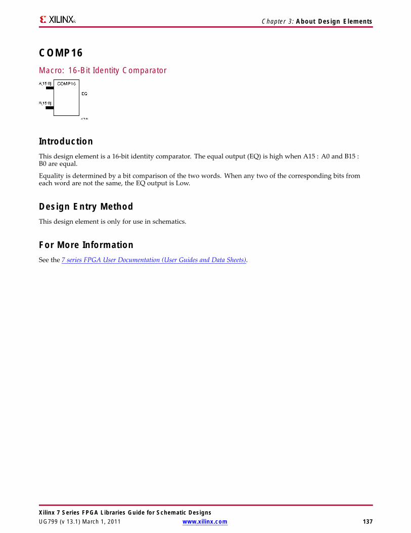
Chapter 3: About Design Elements
COMP16Macro: 16-Bit Identity Comparator
IntroductionThis design element is a 16-bit identity comparator. The equal output (EQ) is high when A15 : A0 and B15 :B0 are equal.
Equality is determined by a bit comparison of the two words. When any two of the corresponding bits fromeach word are not the same, the EQ output is Low.
Design Entry MethodThis design element is only for use in schematics.
For More InformationSee the 7 series FPGA User Documentation (User Guides and Data Sheets).
Xilinx 7 Series FPGA Libraries Guide for Schematic DesignsUG799 (v 13.1) March 1, 2011 www.xilinx.com 137

Chapter 3: About Design Elements
COMP2Macro: 2-Bit Identity Comparator
IntroductionThis design element is a 2-bit identity comparator. The equal output (EQ) is High when the two words A1 : A0and B1 : B0 are equal.
Equality is determined by a bit comparison of the two words. When any two of the corresponding bits fromeach word are not the same, the EQ output is Low.
Design Entry MethodThis design element is only for use in schematics.
For More InformationSee the 7 series FPGA User Documentation (User Guides and Data Sheets).
Xilinx 7 Series FPGA Libraries Guide for Schematic Designs138 www.xilinx.com UG799 (v 13.1) March 1, 2011

Chapter 3: About Design Elements
COMP4Macro: 4-Bit Identity Comparator
IntroductionThis design element is a 4-bit identity comparator. The equal output (EQ) is high when A3 : A0 and B3 : B0 areequal.
Equality is determined by a bit comparison of the two words. When any two of the corresponding bits fromeach word are not the same, the EQ output is Low.
Design Entry MethodThis design element is only for use in schematics.
For More InformationSee the 7 series FPGA User Documentation (User Guides and Data Sheets).
Xilinx 7 Series FPGA Libraries Guide for Schematic DesignsUG799 (v 13.1) March 1, 2011 www.xilinx.com 139
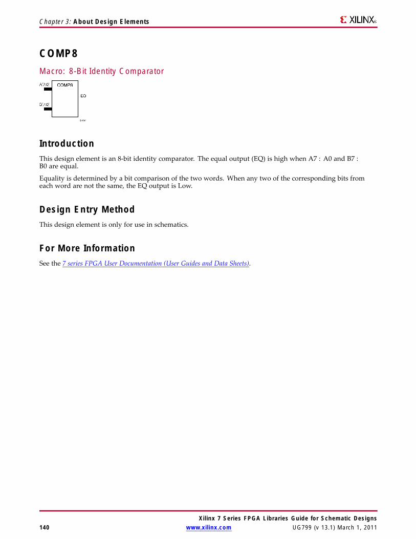
Chapter 3: About Design Elements
COMP8Macro: 8-Bit Identity Comparator
IntroductionThis design element is an 8-bit identity comparator. The equal output (EQ) is high when A7 : A0 and B7 :B0 are equal.
Equality is determined by a bit comparison of the two words. When any two of the corresponding bits fromeach word are not the same, the EQ output is Low.
Design Entry MethodThis design element is only for use in schematics.
For More InformationSee the 7 series FPGA User Documentation (User Guides and Data Sheets).
Xilinx 7 Series FPGA Libraries Guide for Schematic Designs140 www.xilinx.com UG799 (v 13.1) March 1, 2011
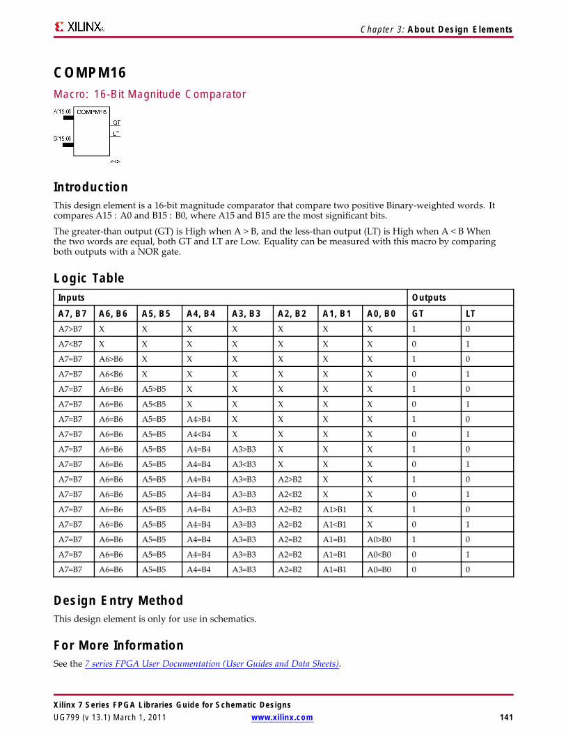
Chapter 3: About Design Elements
COMPM16Macro: 16-Bit Magnitude Comparator
IntroductionThis design element is a 16-bit magnitude comparator that compare two positive Binary-weighted words. Itcompares A15 : A0 and B15 : B0, where A15 and B15 are the most significant bits.
The greater-than output (GT) is High when A > B, and the less-than output (LT) is High when A < B Whenthe two words are equal, both GT and LT are Low. Equality can be measured with this macro by comparingboth outputs with a NOR gate.
Logic TableInputs Outputs
A7, B7 A6, B6 A5, B5 A4, B4 A3, B3 A2, B2 A1, B1 A0, B0 GT LTA7>B7 X X X X X X X 1 0
A7<B7 X X X X X X X 0 1
A7=B7 A6>B6 X X X X X X 1 0
A7=B7 A6<B6 X X X X X X 0 1
A7=B7 A6=B6 A5>B5 X X X X X 1 0
A7=B7 A6=B6 A5<B5 X X X X X 0 1
A7=B7 A6=B6 A5=B5 A4>B4 X X X X 1 0
A7=B7 A6=B6 A5=B5 A4<B4 X X X X 0 1
A7=B7 A6=B6 A5=B5 A4=B4 A3>B3 X X X 1 0
A7=B7 A6=B6 A5=B5 A4=B4 A3<B3 X X X 0 1
A7=B7 A6=B6 A5=B5 A4=B4 A3=B3 A2>B2 X X 1 0
A7=B7 A6=B6 A5=B5 A4=B4 A3=B3 A2<B2 X X 0 1
A7=B7 A6=B6 A5=B5 A4=B4 A3=B3 A2=B2 A1>B1 X 1 0
A7=B7 A6=B6 A5=B5 A4=B4 A3=B3 A2=B2 A1<B1 X 0 1
A7=B7 A6=B6 A5=B5 A4=B4 A3=B3 A2=B2 A1=B1 A0>B0 1 0
A7=B7 A6=B6 A5=B5 A4=B4 A3=B3 A2=B2 A1=B1 A0<B0 0 1
A7=B7 A6=B6 A5=B5 A4=B4 A3=B3 A2=B2 A1=B1 A0=B0 0 0
Design Entry MethodThis design element is only for use in schematics.
For More InformationSee the 7 series FPGA User Documentation (User Guides and Data Sheets).
Xilinx 7 Series FPGA Libraries Guide for Schematic DesignsUG799 (v 13.1) March 1, 2011 www.xilinx.com 141

Chapter 3: About Design Elements
COMPM2Macro: 2-Bit Magnitude Comparator
IntroductionThis design element is a 2-bit magnitude comparator that compare two positive binary-weighted words. Itcompares A1 : A0 and B1 : B0, where A1 and B1 are the most significant bits.
The greater-than output (GT) is High when A > B, and the less-than output (LT) is High when A < B Whenthe two words are equal, both GT and LT are Low. Equality can be measured with this macro by comparingboth outputs with a NOR gate.
Logic TableInputs Outputs
A1 B1 A0 B0 GT LT0 0 0 0 0 0
0 0 1 0 1 0
0 0 0 1 0 1
0 0 1 1 0 0
1 1 0 0 0 0
1 1 1 0 1 0
1 1 0 1 0 1
1 1 1 1 0 0
1 0 X X 1 0
0 1 X X 0 1
Design Entry MethodThis design element is only for use in schematics.
For More InformationSee the 7 series FPGA User Documentation (User Guides and Data Sheets).
Xilinx 7 Series FPGA Libraries Guide for Schematic Designs142 www.xilinx.com UG799 (v 13.1) March 1, 2011
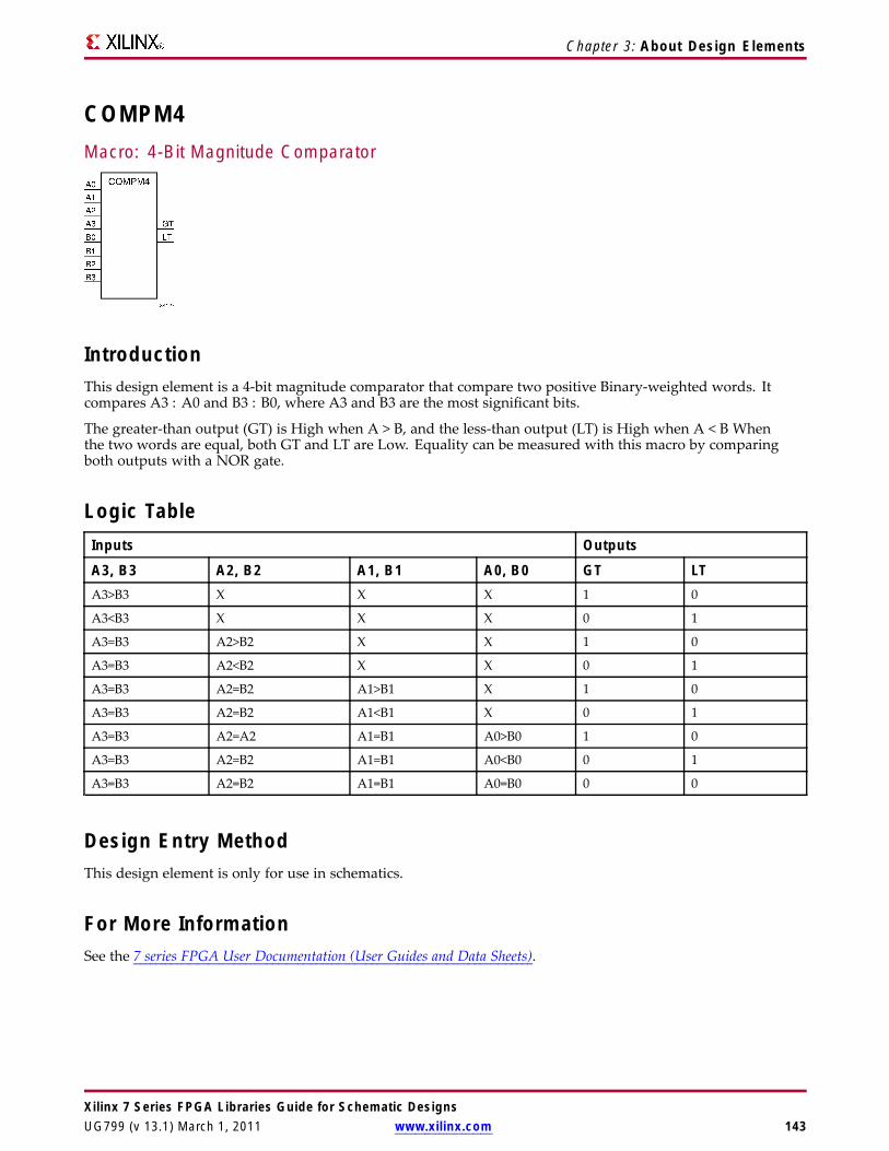
Chapter 3: About Design Elements
COMPM4Macro: 4-Bit Magnitude Comparator
IntroductionThis design element is a 4-bit magnitude comparator that compare two positive Binary-weighted words. Itcompares A3 : A0 and B3 : B0, where A3 and B3 are the most significant bits.
The greater-than output (GT) is High when A > B, and the less-than output (LT) is High when A < B Whenthe two words are equal, both GT and LT are Low. Equality can be measured with this macro by comparingboth outputs with a NOR gate.
Logic TableInputs Outputs
A3, B3 A2, B2 A1, B1 A0, B0 GT LTA3>B3 X X X 1 0
A3<B3 X X X 0 1
A3=B3 A2>B2 X X 1 0
A3=B3 A2<B2 X X 0 1
A3=B3 A2=B2 A1>B1 X 1 0
A3=B3 A2=B2 A1<B1 X 0 1
A3=B3 A2=A2 A1=B1 A0>B0 1 0
A3=B3 A2=B2 A1=B1 A0<B0 0 1
A3=B3 A2=B2 A1=B1 A0=B0 0 0
Design Entry MethodThis design element is only for use in schematics.
For More InformationSee the 7 series FPGA User Documentation (User Guides and Data Sheets).
Xilinx 7 Series FPGA Libraries Guide for Schematic DesignsUG799 (v 13.1) March 1, 2011 www.xilinx.com 143

Chapter 3: About Design Elements
COMPM8Macro: 8-Bit Magnitude Comparator
IntroductionThis design element is an 8-bit magnitude comparator that compare two positive Binary-weighted words. Itcompares A7 : A0 and B7 : B0, where A7 and B7 are the most significant bits.
The greater-than output (GT) is High when A > B, and the less-than output (LT) is High when A < B Whenthe two words are equal, both GT and LT are Low. Equality can be measured with this macro by comparingboth outputs with a NOR gate.
Logic TableInputs Outputs
A7, B7 A6, B6 A5, B5 A4, B4 A3, B3 A2, B2 A1, B1 A0, B0 GT LTA7>B7 X X X X X X X 1 0
A7<B7 X X X X X X X 0 1
A7=B7 A6>B6 X X X X X X 1 0
A7=B7 A6<B6 X X X X X X 0 1
A7=B7 A6=B6 A5>B5 X X X X X 1 0
A7=B7 A6=B6 A5<B5 X X X X X 0 1
A7=B7 A6=B6 A5=B5 A4>B4 X X X X 1 0
A7=B7 A6=B6 A5=B5 A4<B4 X X X X 0 1
A7=B7 A6=B6 A5=B5 A4=B4 A3>B3 X X X 1 0
A7=B7 A6=B6 A5=B5 A4=B4 A3<B3 X X X 0 1
A7=B7 A6=B6 A5=B5 A4=B4 A3=B3 A2>B2 X X 1 0
A7=B7 A6=B6 A5=B5 A4=B4 A3=B3 A2<B2 X X 0 1
A7=B7 A6=B6 A5=B5 A4=B4 A3=B3 A2=B2 A1>B1 X 1 0
A7=B7 A6=B6 A5=B5 A4=B4 A3=B3 A2=B2 A1<B1 X 0 1
A7=B7 A6=B6 A5=B5 A4=B4 A3=B3 A2=B2 A1=B1 A0>B0 1 0
A7=B7 A6=B6 A5=B5 A4=B4 A3=B3 A2=B2 A1=B1 A0<B0 0 1
A7=B7 A6=B6 A5=B5 A4=B4 A3=B3 A2=B2 A1=B1 A0=B0 0 0
Design Entry MethodThis design element is only for use in schematics.
For More InformationSee the 7 series FPGA User Documentation (User Guides and Data Sheets).
Xilinx 7 Series FPGA Libraries Guide for Schematic Designs144 www.xilinx.com UG799 (v 13.1) March 1, 2011

Chapter 3: About Design Elements
COMPMC16Macro: 16-Bit Magnitude Comparator
IntroductionThis design element is a 16-bit, magnitude comparator that compares two positive Binary weighted words A15 :A0 and B15 : B0, where A15 and B15 are the most significant bits.
This comparator is implemented using carry logic with relative location constraints to ensure efficient logicplacement.
The greater-than output (GT) is High when A>B, and the less-than output (LT) is High when A<B. When thetwo words are equal, both GT and LT are Low. Equality can be flagged with this macro by connecting bothoutputs to a NOR gate.
Logic TableInputs Outputs
A7, B7 A6, B6 A5, B5 A4, B4 A3, B3 A2, B2 A1, B1 A0, B0 GT LTA7>B7 X X X X X X X 1 0
A7<B7 X X X X X X X 0 1
A7=B7 A6>B6 X X X X X X 1 0
A7=B7 A6<B6 X X X X X X 0 1
A7=B7 A6=B6 A5>B5 X X X X X 1 0
A7=B7 A6=B6 A5<B5 X X X X X 0 1
A7=B7 A6=B6 A5=B5 A4>B4 X X X X 1 0
A7=B7 A6=B6 A5=B5 A4<B4 X X X X 0 1
A7=B7 A6=B6 A5=B5 A4=B4 A3>B3 X X X 1 0
A7=B7 A6=B6 A5=B5 A4=B4 A3<B3 X X X 0 1
A7=B7 A6=B6 A5=B5 A4=B4 A3=B3 A2>B2 X X 1 0
A7=B7 A6=B6 A5=B5 A4=B4 A3=B3 A2<B2 X X 0 1
A7=B7 A6=B6 A5=B5 A4=B4 A3=B3 A2=B2 A1>B1 X 1 0
A7=B7 A6=B6 A5=B5 A4=B4 A3=B3 A2=B2 A1<B1 X 0 1
A7=B7 A6=B6 A5=B5 A4=B4 A3=B3 A2=B2 A1=B1 A0>B0 1 0
A7=B7 A6=B6 A5=B5 A4=B4 A3=B3 A2=B2 A1=B1 A0<B0 0 1
A7=B7 A6=B6 A5=B5 A4=B4 A3=B3 A2=B2 A1=B1 A0=B0 0 0
Design Entry MethodThis design element is only for use in schematics.
Xilinx 7 Series FPGA Libraries Guide for Schematic DesignsUG799 (v 13.1) March 1, 2011 www.xilinx.com 145

Chapter 3: About Design Elements
For More InformationSee the 7 series FPGA User Documentation (User Guides and Data Sheets).
Xilinx 7 Series FPGA Libraries Guide for Schematic Designs146 www.xilinx.com UG799 (v 13.1) March 1, 2011

Chapter 3: About Design Elements
COMPMC8Macro: 8-Bit Magnitude Comparator
IntroductionThis design element is an 8-bit, magnitude comparator that compares two positive Binaryweighted words A7 :A0 and B7 : B0, where A7 and B7 are the most significant bits.
This comparator is implemented using carry logic with relative location constraints to ensure efficient logicplacement.
The greater-than output (GT) is High when A>B, and the less-than output (LT) is High when A<B. When thetwo words are equal, both GT and LT are Low. Equality can be flagged with this macro by connecting bothoutputs to a NOR gate.
Logic TableInputs Outputs
A7, B7 A6, B6 A5, B5 A4, B4 A3, B3 A2, B2 A1, B1 A0, B0 GT LTA7>B7 X X X X X X X 1 0
A7<B7 X X X X X X X 0 1
A7=B7 A6>B6 X X X X X X 1 0
A7=B7 A6<B6 X X X X X X 0 1
A7=B7 A6=B6 A5>B5 X X X X X 1 0
A7=B7 A6=B6 A5<B5 X X X X X 0 1
A7=B7 A6=B6 A5=B5 A4>B4 X X X X 1 0
A7=B7 A6=B6 A5=B5 A4<B4 X X X X 0 1
A7=B7 A6=B6 A5=B5 A4=B4 A3>B3 X X X 1 0
A7=B7 A6=B6 A5=B5 A4=B4 A3<B3 X X X 0 1
A7=B7 A6=B6 A5=B5 A4=B4 A3=B3 A2>B2 X X 1 0
A7=B7 A6=B6 A5=B5 A4=B4 A3=B3 A2<B2 X X 0 1
A7=B7 A6=B6 A5=B5 A4=B4 A3=B3 A2=B2 A1>B1 X 1 0
A7=B7 A6=B6 A5=B5 A4=B4 A3=B3 A2=B2 A1<B1 X 0 1
A7=B7 A6=B6 A5=B5 A4=B4 A3=B3 A2=B2 A1=B1 A0>B0 1 0
A7=B7 A6=B6 A5=B5 A4=B4 A3=B3 A2=B2 A1=B1 A0<B0 0 1
A7=B7 A6=B6 A5=B5 A4=B4 A3=B3 A2=B2 A1=B1 A0=B0 0 0
Design Entry MethodThis design element is only for use in schematics.
Xilinx 7 Series FPGA Libraries Guide for Schematic DesignsUG799 (v 13.1) March 1, 2011 www.xilinx.com 147

Chapter 3: About Design Elements
For More InformationSee the 7 series FPGA User Documentation (User Guides and Data Sheets).
Xilinx 7 Series FPGA Libraries Guide for Schematic Designs148 www.xilinx.com UG799 (v 13.1) March 1, 2011

Chapter 3: About Design Elements
D2_4EMacro: 2- to 4-Line Decoder/Demultiplexer with Enable
IntroductionThis design element is a decoder/demultiplexer. When the enable (E) input of this element is High, one of fouractive-High outputs (D3 : D0) is selected with a 2-bit binary address (A1 : A0) input. The non-selected outputsare Low. Also, when the E input is Low, all outputs are Low. In demultiplexer applications, the E input is thedata input.
Logic TableInputs OutputsA1 A0 E D3 D2 D1 D0X X 0 0 0 0 0
0 0 1 0 0 0 1
0 1 1 0 0 1 0
1 0 1 0 1 0 0
1 1 1 1 0 0 0
Design Entry MethodThis design element is only for use in schematics.
For More InformationSee the 7 series FPGA User Documentation (User Guides and Data Sheets).
Xilinx 7 Series FPGA Libraries Guide for Schematic DesignsUG799 (v 13.1) March 1, 2011 www.xilinx.com 149
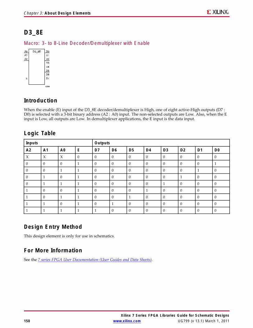
Chapter 3: About Design Elements
D3_8EMacro: 3- to 8-Line Decoder/Demultiplexer with Enable
IntroductionWhen the enable (E) input of the D3_8E decoder/demultiplexer is High, one of eight active-High outputs (D7 :D0) is selected with a 3-bit binary address (A2 : A0) input. The non-selected outputs are Low. Also, when the Einput is Low, all outputs are Low. In demultiplexer applications, the E input is the data input.
Logic TableInputs OutputsA2 A1 A0 E D7 D6 D5 D4 D3 D2 D1 D0X X X 0 0 0 0 0 0 0 0 0
0 0 0 1 0 0 0 0 0 0 0 1
0 0 1 1 0 0 0 0 0 0 1 0
0 1 0 1 0 0 0 0 0 1 0 0
0 1 1 1 0 0 0 0 1 0 0 0
1 0 0 1 0 0 0 1 0 0 0 0
1 0 1 1 0 0 1 0 0 0 0 0
1 1 0 1 0 1 0 0 0 0 0 0
1 1 1 1 1 0 0 0 0 0 0 0
Design Entry MethodThis design element is only for use in schematics.
For More InformationSee the 7 series FPGA User Documentation (User Guides and Data Sheets).
Xilinx 7 Series FPGA Libraries Guide for Schematic Designs150 www.xilinx.com UG799 (v 13.1) March 1, 2011
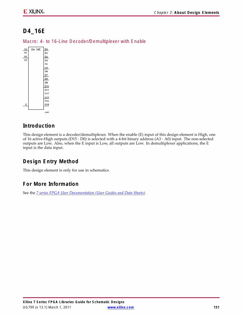
Chapter 3: About Design Elements
D4_16EMacro: 4- to 16-Line Decoder/Demultiplexer with Enable
IntroductionThis design element is a decoder/demultiplexer. When the enable (E) input of this design element is High, oneof 16 active-High outputs (D15 : D0) is selected with a 4-bit binary address (A3 : A0) input. The non-selectedoutputs are Low. Also, when the E input is Low, all outputs are Low. In demultiplexer applications, the Einput is the data input.
Design Entry MethodThis design element is only for use in schematics.
For More InformationSee the 7 series FPGA User Documentation (User Guides and Data Sheets).
Xilinx 7 Series FPGA Libraries Guide for Schematic DesignsUG799 (v 13.1) March 1, 2011 www.xilinx.com 151

Chapter 3: About Design Elements
DCIRESETPrimitive: Digitially Controlled Impedance Reset Component
IntroductionThis design element is used to reset the Digitially Controlled Impedance (DCI) state machine after configurationhas been completed. By toggling the RST input to the DCIRESET primitive while the device is operating, the DCIstate-machine is reset and both phases of impedance adjustment proceed in succession. All I/Os using DCI willbe unavailable until the LOCKED output from the DCIRESET block is asserted
Port DescriptionsPort Type Width FunctionLOCKED Output 1 DCI state-machine LOCK status output.
When low, DCI I/O impedence is beingcalibrated and are unavailable.Upon alow-to-high assertion, DCI I/Os are availablefor use.
RST Input 1 Active-high asynchronous reset input toDCI state-machine. After RST is asserted,I/Os utilizing DCI will be unavailable untilLOCKED is asserted.
Design Entry MethodThis design element can be used in schematics.
For More InformationSee the 7 series FPGA User Documentation (User Guides and Data Sheets).
Xilinx 7 Series FPGA Libraries Guide for Schematic Designs152 www.xilinx.com UG799 (v 13.1) March 1, 2011

Chapter 3: About Design Elements
DEC_CC16Macro: 16-Bit Active Low Decoder
IntroductionThis design element is a 16-bit decoder that is used to build wide-decoder functions. It is implemented bycascading CY_MUX elements driven by look-up tables (LUTs). The C_IN pin can only be driven by the output (O)of a previous decode stage. When one or more of the inputs (A) are Low, the output is Low. When all the inputsare High and the C_IN input is High, the output is High. You can decode patterns by adding inverters to inputs.
Logic TableInputs Outputs
A0 A1 … Az C_IN O1 1 1 1 1 1
X X X X 0 0
0 X X X X 0
X 0 X X X 0
X X X 0 X 0
z = 3 for DEC_CC4; z = 7 for DEC_CC8; z = 15 for DEC_CC16
Design Entry MethodThis design element is only for use in schematics.
For More InformationSee the 7 series FPGA User Documentation (User Guides and Data Sheets).
Xilinx 7 Series FPGA Libraries Guide for Schematic DesignsUG799 (v 13.1) March 1, 2011 www.xilinx.com 153

Chapter 3: About Design Elements
DEC_CC4Macro: 4-Bit Active Low Decoder
IntroductionThis design element is a 4-bit decoder that is used to build wide-decoder functions. It is implemented bycascading CY_MUX elements driven by look-up tables (LUTs). The C_IN pin can only be driven by the output (O)of a previous decode stage. When one or more of the inputs (A) are Low, the output is Low. When all the inputsare High and the C_IN input is High, the output is High. You can decode patterns by adding inverters to inputs.
Logic TableInputs Outputs
A0 A1 … Az C_IN O1 1 1 1 1 1
X X X X 0 0
0 X X X X 0
X 0 X X X 0
X X X 0 X 0
z = 3 for DEC_CC4; z = 7 for DEC_CC8; z = 15 for DEC_CC16
Design Entry MethodThis design element is only for use in schematics.
For More InformationSee the 7 series FPGA User Documentation (User Guides and Data Sheets).
Xilinx 7 Series FPGA Libraries Guide for Schematic Designs154 www.xilinx.com UG799 (v 13.1) March 1, 2011
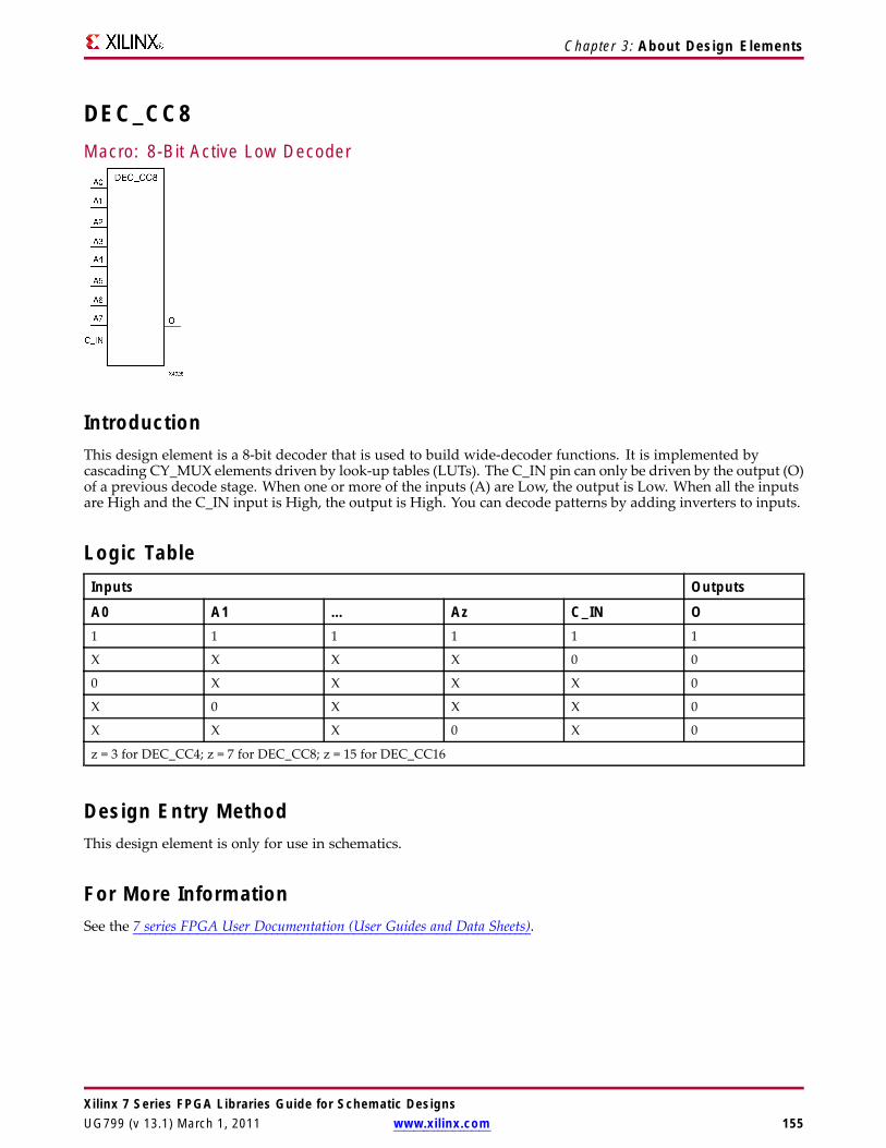
Chapter 3: About Design Elements
DEC_CC8Macro: 8-Bit Active Low Decoder
IntroductionThis design element is a 8-bit decoder that is used to build wide-decoder functions. It is implemented bycascading CY_MUX elements driven by look-up tables (LUTs). The C_IN pin can only be driven by the output (O)of a previous decode stage. When one or more of the inputs (A) are Low, the output is Low. When all the inputsare High and the C_IN input is High, the output is High. You can decode patterns by adding inverters to inputs.
Logic TableInputs Outputs
A0 A1 … Az C_IN O1 1 1 1 1 1
X X X X 0 0
0 X X X X 0
X 0 X X X 0
X X X 0 X 0
z = 3 for DEC_CC4; z = 7 for DEC_CC8; z = 15 for DEC_CC16
Design Entry MethodThis design element is only for use in schematics.
For More InformationSee the 7 series FPGA User Documentation (User Guides and Data Sheets).
Xilinx 7 Series FPGA Libraries Guide for Schematic DesignsUG799 (v 13.1) March 1, 2011 www.xilinx.com 155

Chapter 3: About Design Elements
DNA_PORTPrimitive: Device DNA Access Port
IntroductionThe DNA_PORT allows access to a dedicated shift register that can be loaded with the Device DNA data bits(factory-programmed, read-only unique ID) for a given 7 series device. In addition to shifting out the DNA databits, this component allows for the inclusion of supplemental bits of your data, or allows for the DNA datato rollover (repeat DNA data after initial data has been shifted out). This component is primarily used inconjunction with other circuitry to build added copy protection for the FPGA bitstream from possible theft.Connect all inputs and outputs to the design to ensure proper operation. To access the Device DNA data, youmust first load the shift register by setting the active high READ signal for one clock cycle. After the shift registeris loaded, the data can be synchronously shifted out by enabling the active high SHIFT input and capturingthe data out the DOUT output port. Additional data can be appended to the end of the 57-bit shift register byconnecting the appropriate logic to the DIN port. If DNA data rollover is desired, connect the DOUT portdirectly to the DIN port to allow for the same data to be shifted out after completing the 57-bit shift operation. Ifno additional data is necessary, the DIN port can be tied to a logic zero. The attribute SIM_DNA_VALUE canbe optionally set to allow for simulation of a possible DNA data sequence. By default, the Device DNA databits are all zeros in the simulation model.
Port DescriptionsPort Type Width FunctionCLK Input 1 Clock input.
DIN Input 1 User data input pin.
DOUT Output 1 DNA output data.
READ Input 1 Active high load DNA, active low read input.
SHIFT Input 1 Active high shift enable input.
Design Entry MethodThis design element can be used in schematics.
Available AttributesAttribute Type Allowed Values Default DescriptionSIM_DNA_VALUE HEX all zeros to all ones all zeros Specifies the Pre-programmed factory ID
value.
Xilinx 7 Series FPGA Libraries Guide for Schematic Designs156 www.xilinx.com UG799 (v 13.1) March 1, 2011

Chapter 3: About Design Elements
For More InformationSee the 7 series FPGA User Documentation (User Guides and Data Sheets).
Xilinx 7 Series FPGA Libraries Guide for Schematic DesignsUG799 (v 13.1) March 1, 2011 www.xilinx.com 157
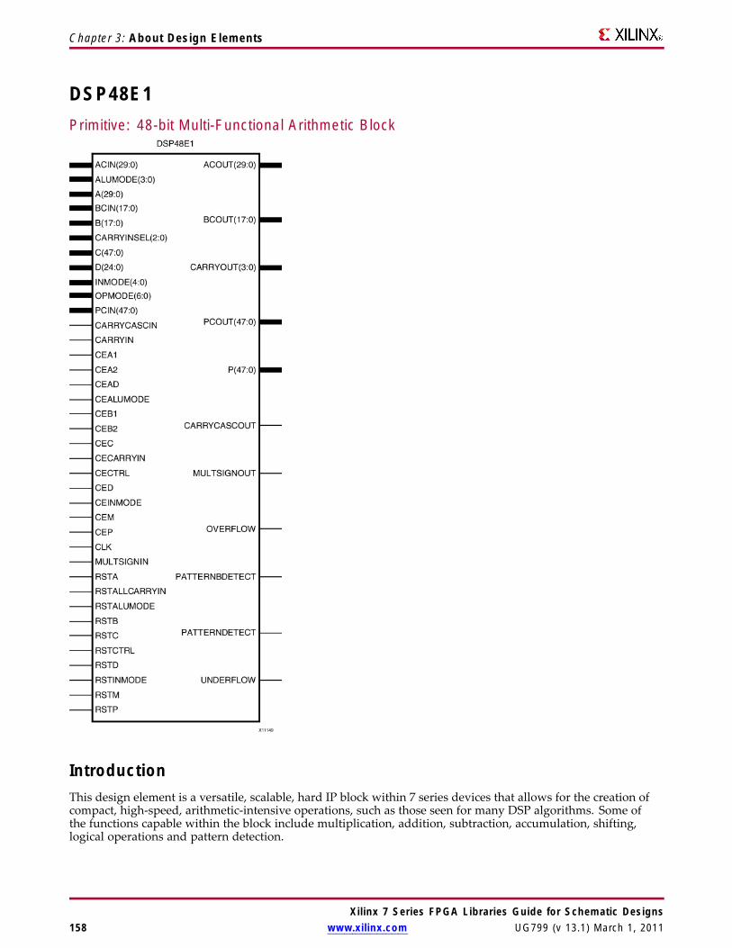
Chapter 3: About Design Elements
DSP48E1Primitive: 48-bit Multi-Functional Arithmetic Block
IntroductionThis design element is a versatile, scalable, hard IP block within 7 series devices that allows for the creation ofcompact, high-speed, arithmetic-intensive operations, such as those seen for many DSP algorithms. Some ofthe functions capable within the block include multiplication, addition, subtraction, accumulation, shifting,logical operations and pattern detection.
Xilinx 7 Series FPGA Libraries Guide for Schematic Designs158 www.xilinx.com UG799 (v 13.1) March 1, 2011

Chapter 3: About Design Elements
Port DescriptionsPort Type Width FunctionA<29:0> Input 30 A[24:0] is the A input of the multiplier. A[29:0] are the most
significant bits (MSBs) of the A:B concatenated input to thesecond-stage adder/subtractor or logic function or a 25-bit datainput to the pre-adder.
ACIN<29:0> Input 30 Cascaded data input from ACOUT of previous DSP48E1 slice(muxed with A). If not used, tie port to all zeros.
ACOUT<29:0> Output 30 Cascaded data output to ACIN of next DSP48E1 slice. If not used,leave unconnected.
ALUMODE<3:0> Input 4 Controls the selection of the logic function in the DSP48E1 slice.
B<17:0> Input 18 The B input of the multiplier. B[17:0] are the least significantbits (LSBs) of the A:B concatenated input to the second-stageadder/subtractor logic function.
BCIN<17:0> Input 18 Cascaded data input from BCOUT of previous DSP48E1 slice(muxed with B). If not used, tie port to all zeros.
BCOUT<17:0> Output 18 Cascaded data output to BCIN of next DSP48E1 slice. If not used,leave unconnected.
C<47:0> Input 48 Data input to the second-stage adder/subtractor, pattern detector, orlogic function.
CARRYCASCIN Input 1 Cascaded carry input from CARRYCASCOUT of previous DSP48E1slice.
CARRYCASCOUT Output 1 Cascaded carry output to CARRYCASCIN of next DSP48E1 slice.This signal is internally fed back into the CARRYINSEL multiplexerinput of the same DSP48E1 slice.
CARRYIN Input 1 Carry input from the FPGA logic.
CARRYINSEL<2:0> Input 3 Selects the carry source:
• 0 1 1 - PCIN[47] - Rounding PCIN (round towards zero)
• 1 0 0 - CARRYCASCOUT - For larger add/sub/acc (sequentialoperation via internal feedback). Must select with PREG = 1
• 1 0 1 - ~P[47] - Rounding P (round towards infinity). Must selectwith PREG = 1
• 1 1 0 - A[24] - XNOR B[17] Rounding A x B 1 1 1 - P[47] - Forrounding P (round towards zero). Must select with PREG = 1
CARRYOUT<3:0> Output 4 4-bit carry output from each 12-bit field of the accumulate/adder/logicunit. Normal 48-bit operation uses only CARRYOUT3. SIMDoperation can use four carry out bits (CARRYOUT[3:0]).
CEAD Input 1 Active high, clock enable for the pre-adder output AD pipelineregister. Tie to logic one if not used and ADREG=1. Tie to logiczero if ADREG=0.
CEALUMODE Input 1 Active High, Clock enable for ALUMODE (control inputs) registers(ALUMODEREG=1). Tie to logic one if not used.
CEA1 Input 1 Active high, clock enable for the first A (input) register. This port isonly used if AREG = 2 or INMODE0 = 1. Tie to logic one if not usedand AREG=2. Tie to logic zero if AREG=0 or 1. When two registersare used, this is the first sequentially. When Dynamic AB Access isused, this clock enable is applied for INMODE[0]=1.
Xilinx 7 Series FPGA Libraries Guide for Schematic DesignsUG799 (v 13.1) March 1, 2011 www.xilinx.com 159

Chapter 3: About Design Elements
Port Type Width FunctionCEA2 Input 1 Active high, clock enable for the second A (input) register. This
port is only used if AREG = 1 or 2. Tie to logic one if not used andAREG=1 or 2. Tie to logic zero if AREG=0. When two registers areused, this is the second sequentially. When one register is used(AREG=1), CEA2 is the clock enable.
CEB1 Input 1 Active high, Clock enable for the first B (input) register. This port isonly used if BREG = 2 or INMODE4 = 1. Tie to logic one if not usedand BREG=2. Tie to logic zero if BREG=0 or 1. When two registersare used, this is the first sequentially. When Dynamic AB Access isused, this clock enable is applied for INMODE[4]=1.
CEB2 Input 1 Active high, clock enable for the second B (input) register. This portis only used if BREG = 1 or 2. Tie to logic one if not used and BREG=1or 2. Tie to logic zero if BREG=0. When two registers are used, this isthe second sequentially. When one register isused (BREG=1), CEB2is the clock enable.
CEC Input 1 Active High, Clock enable for the C (input) register. (CREG=1). Tieto logic one if not used.
CECARRYIN Input 1 Active high, clock enable for the CARRYIN (input from fabric)register (CARRYINREG=1). Tie to logic one if not used.
CECTRL Input 1 Active high, clock enable for the OPMODE and CARRYINSEL(control inputs) registers (OPMODEREG=1 or CARRYINSELREG=1).Tie to logic one if not used.
CED Input 1 Active high, Clock enable for the D (input) registers (DREG=1). Tieto logic one if not used.
CEINMODE Input 1 Active high, clock enable for the INMODE control input registers(INMODEREG=1). Tie to logic one if not used.
CEM Input 1 Active high, Clock enable for the post-multiply M (pipeline) registerand the internal multiply round CARRYIN register (MREG=1). Tieto logic one if not used.
CEP Input 1 Active high, clock enable for the P (output) register (PREG=1). Tieto logic one if not used.
CLK Input 1 This port is the DSP48E1 input clock, common to all internal registersand flip-flops.
D<24:0> Input 25 25-bit data input to the pre-adder or alternative input to themultiplier. The pre-adder implements D + A as determined by theINMODE3 signal.
INMODE<4:0> Input 5 These five control bits select the functionality of the pre-adder, theA, B, and D inputs, and the input registers. These bits should be tiedto all zeroes if not used.
MULTSIGNIN Input 1 Sign of the multiplied result from the previous DSP48E1 slice forMACC extension. Either connect to the MULTSIGNOUT of anotherDSP block or tie to ground if not used.
MULTSIGNOUT Output 1 Sign of the multiplied result cascaded to the next DSP48E1 slice forMACC extension. Either connect to the MULTSIGNIN of anotherDSP block or tie to ground if not used.
OPMODE<6:0> Input 7 Controls the input to the X, Y, and Z multiplexers in the DSP48E1slice dictating the operation or function of the DSP slice.
OVERFLOW Output 1 Active high Overflow indicator when used with the appropriatesetting of the pattern detector and PREG=1.
P<47:0> Output 48 Data output from second stage adder/subtractor or logic function.
PATTERNBDETECT Output 1 Active high match indicator between P[47:0] and the pattern bar.
Xilinx 7 Series FPGA Libraries Guide for Schematic Designs160 www.xilinx.com UG799 (v 13.1) March 1, 2011

Chapter 3: About Design Elements
Port Type Width FunctionPATTERNDETECT Output 1 Active high Match indicator between P[47:0] and the pattern gated
by the MASK. Result arrives on the same cycle as P.
PCIN<47:0> Input 48 Cascaded data input from PCOUT of previous DSP48E1 slice toadder. If used, connect to PCOUT of upstream cascaded DSP slice.If not used, tie port to all zeros.
PCOUT<47:0> Output 48 Cascaded data output to PCIN of next DSP48E1 slice. If used,connect to PCIN of downstream cascaded DSP slice. If not used,leave unconnected.
RSTA Input 1 Active high, synchronous Reset for both A (input) registers (AREG=1or 2). Tie to logic zero if not used.
RSTALLCARRYIN Input 1 Active high, synchronous reset for the Carry (internal path) and theCARRYIN registers (CARRYINREG=1). Tie to logic zero if not used.
RSTALUMODE Input 1 Active high, synchronous Reset for ALUMODE (control inputs)registers (ALUMODEREG=1). Tie to logic zero if not used.
RSTB Input 1 Active high, synchronous Reset for both B (input) registers (BREG=1or 2). | Tie to logic zero if not used.
RSTC Input 1 Active high, synchronous reset for the C (input) registers (CREG=1).Tie to logic zero if not used.
RSTCTRL Input 1 Active High, synchronous reset for OPMODE and CARRYINSEL(control inputs) registers. (OPMODEREG=1 and/orCARRYINSELREG=1). Tie to logic zero if not used.
RSTD Input 1 Active high, synchronous reset for the D (input) register and forthe pre-adder (output) AD pipeline register (DREG=1 and/orADREG=1). Tie to logic zero if not used.
RSTINMODE Input 1 Active high, synchronous reset for the INMODE (control input)registers (INMODEREG=1). Tie to logic zero if not used.
RSTM Input 1 Active high, synchronous reset for the M (pipeline) registers(MREG=1). Tie to logic zero if not used.
RSTP Input 1 Active high, synchronous reset for the P (output) registers (PREG=1).Tie to logic zero if not used.
UNDERFLOW Output 1 Active high underflow indicator when used with the appropriatesetting of the pattern detector and PREG = 1.
Design Entry MethodThis design element can be used in schematics.
Available AttributesAttribute Type Allowed Values Default DescriptionA_INPUT STRING “DIRECT”,
“CASCADE”“DIRECT” Selects the input to the A port between parallel
input ("DIRECT") or the cascaded input from theprevious slice ("CASCADE").
Xilinx 7 Series FPGA Libraries Guide for Schematic DesignsUG799 (v 13.1) March 1, 2011 www.xilinx.com 161

Chapter 3: About Design Elements
Attribute Type Allowed Values Default DescriptionACASCREG DECIMAL 1, 0, 2 1 In conjunction with AREG, selects the number of
A input registers on the A cascade path, ACOUT.This attribute must be equal to or one less thanthe AREG value:
• AREG = 0: ACASCREG must be 0
• AREG = 1: ACASCREG must be 1
• AREG = 2: ACASCREG can be 1 or 2
ADREG DECIMAL 1, 0 1 Selects the number of AD pipeline registers. Setto 1 to use the AD pipeline registers.
ALUMODEREG DECIMAL 1, 0 1 Selects the number of ALUMODE input registers.Set to 1 to register the ALUMODE inputs.
AREG DECIMAL 1, 0, 2 1 Selects the number of A input pipeline registers.
AUTORESET_PATDET
STRING “NO_RESET”,“RESET_MATCH”,“RESET_NOT_MATCH”
“NO_RESET” Automatically resets the P Register (accumulatedvalue or counter value) on the next clockcycle, if a pattern detect event has occurred onthis clock cycle. The "RESET_MATCH" and"RESET_NOT_MATCH" settings distinguishbetween whether the DSP48E1 slice should causean auto reset of the P Register on the next cycle:- if the pattern is matched or - whenever thepattern is not matched on the current cycle butwas matched on the previous clock cycle
B_INPUT STRING “DIRECT”,“CASCADE”
“DIRECT” Selects the input to the B port between parallelinput ("DIRECT") or the cascaded input from theprevious slice ("CASCADE").
BCASCREG DECIMAL 1, 0, 2 1 In conjunction with BREG, selects the number ofB input registers on the B cascade path, BCOUT.This attribute must be equal to or one less thanthe BREG value:
• BREG = 0: BCASCREG must be 0
• BREG = 1: BCASCREG must be 1
• BREG = 2: BCASCREG can be 1 or 2
BREG DECIMAL 1, 0, 2 1 Selects the number of B input registers.
CARRYINREG DECIMAL 1, 0 1 Selects the number of CARRYIN input registers.Set to 1 to register the CARRYIN inputs.
CARRYINSELREG DECIMAL 1, 0 1 Selects the number of CARRYINSEL inputregisters. Set to 1 to register the CARRYINSELinputs.
CREG DECIMAL 1, 0 1 Selects the number of C input registers. Set to 1to register the C inputs.
DREG DECIMAL 1, 0 1 Selects the number of D input registers. Set to 1to register the D inputs.
INMODEREG DECIMAL 1, 0 1 Selects the number of INMODE input registers.Set to 1 to register the INMODE inputs.
MASK HEX all zeros to allones
all ones This 48-bit value is used to mask out certain bitsduring a pattern detection. When a MASK bit isset to 1, the corresponding pattern bit is ignored.When a MASK bit is set to 0, the pattern bit iscompared.
Xilinx 7 Series FPGA Libraries Guide for Schematic Designs162 www.xilinx.com UG799 (v 13.1) March 1, 2011

Chapter 3: About Design Elements
Attribute Type Allowed Values Default DescriptionMREG DECIMAL 1, 0 1 Selects the number of multiplier output (M)
pipeline register stages. Set to 1 to use the Mpipeline registers.
OPMODEREG DECIMAL 1, 0 1 Selects the number of OPMODE input registers.Set to 1 to register the OPMODE inputs.
PATTERN HEX all zeros to allones
all zeros This 48-bit value is used in the pattern detector.
PREG DECIMAL 1, 0 1 Selects the number of P output registers. Set to 1to register the P outputs. The registered outputswill include CARRYOUT, CARRYCASCOUT,MULTSIGNOUT, PATTERNB_DETECT,PATTERN_DETECT, and PCOUT.
SEL_MASK STRING “MASK”, “C”,“ROUNDING_MODE1”,“ROUNDING_MODE2”
“MASK” Selects the mask to be used for the patterndetector. The “C” and “MASK” settingsare for standard uses of the patterndetector (counter, overflow detection,etc.). “ROUNDING_MODE1” (Cbar left shiftedby 1) and “ROUNDING_MODE2” (C-bar leftshifted by 2) select special masks based off of theoptionally registered C port. These roundingmodes can be used to implement convergentrounding in the DSP48E1 slice using the patterndetector.
SEL_PATTERN STRING “PATTERN”, “C” “PATTERN” Selects the input source for the pattern field. Theinput source can either be a 48-bit dynamic Cinput or a 48-bit static PATTERN attribute field.
USE_DPORT BOOLEAN FALSE, TRUE FALSE Determines whether the pre-adder and the DPort are used or not.
USE_MULT STRING “MULTIPLY”,“DYNAMIC”,“NONE”
“MULTIPLY” Selects usage of the multiplier. Set to "NONE" tosave power when using only the Adder/LogicUnit. The "DYNAMIC" setting indicates thatthe user is switching between A*B and A:Boperations on the fly and therefore needs to getthe worst-case timing of the two paths.
USE_PATTERN_DETECT
STRING “NO_PATDET”,“PATDET”
“NO_PATDET” Selects whether the pattern detector and relatedfeatures are used ("PATDET") or not used("NO_PATDET"). This attribute is used for speedspecification and Simulation Model purposesonly.
USE_SIMD STRING “ONE48”,“FOUR12”,“TWO24”
ONE48 Selects the mode of operation for theadder/subtractor. The attribute setting can beone 48-bit adder mode ("ONE48"), two 24- bitadder mode ("TWO24"), or four 12-bit addermode ("FOUR12"). Selecting "ONE48" modeis compatible with Virtex-5 DSP48 operationand is not actually a true SIMD mode. TypicalMultiply-Add operations are supported whenthe mode is set to "ONE48". When either"TWO24" or "FOUR12" mode is selected, themultiplier must not be used, and USE_MULTmust be set to "NONE".
For More InformationSee the 7 series FPGA User Documentation (User Guides and Data Sheets).
Xilinx 7 Series FPGA Libraries Guide for Schematic DesignsUG799 (v 13.1) March 1, 2011 www.xilinx.com 163

Chapter 3: About Design Elements
EFUSE_USRPrimitive: 32-bit non-volatile design ID
IntroductionProvides internal access to the 32 non-volatile , user-programmable eFUSE bits.
Port DescriptionsPort Type Width FunctionEFUSEUSR<31:0> Output 32 User eFUSE register value output.
Design Entry MethodThis design element can be used in schematics.
Available AttributesAttribute Type Allowed Values Default DescriptionSIM_EFUSE_VALUE HEX all zeros to all ones all zeros Value of the 32-bit non-volatile value
used in simulation.
For More InformationSee the 7 series FPGA User Documentation (User Guides and Data Sheets).
Xilinx 7 Series FPGA Libraries Guide for Schematic Designs164 www.xilinx.com UG799 (v 13.1) March 1, 2011

Chapter 3: About Design Elements
FDD Flip-Flop
IntroductionThis design element is a D-type flip-flop with data input (D) and data output (Q). The data on the D inputs isloaded into the flip-flop during the Low-to-High clock (C) transition.
This flip-flop is asynchronously cleared, outputs Low, when power is applied. For FPGA devices, power-onconditions are simulated when global set/reset (GSR) is active. GSR defaults to active-High but can be invertedby adding an inverter in front of the GSR input of the appropriate STARTUP_architecture symbol.
Logic TableInputs Outputs
D C Q0 ↑ 0
1 ↑ 1
Design Entry MethodThis design element is only for use in schematics.
Available Attributes
Attribute TypeAllowedValues Default Description
INIT Binary 0, 1 0 Sets the initial value of Q output after configuration
For More InformationSee the 7 series FPGA User Documentation (User Guides and Data Sheets).
Xilinx 7 Series FPGA Libraries Guide for Schematic DesignsUG799 (v 13.1) March 1, 2011 www.xilinx.com 165
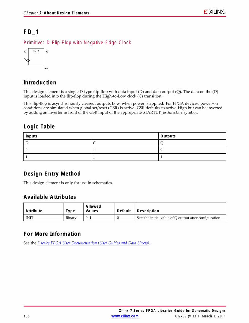
Chapter 3: About Design Elements
FD_1Primitive: D Flip-Flop with Negative-Edge Clock
IntroductionThis design element is a single D-type flip-flop with data input (D) and data output (Q). The data on the (D)input is loaded into the flip-flop during the High-to-Low clock (C) transition.
This flip-flop is asynchronously cleared, outputs Low, when power is applied. For FPGA devices, power-onconditions are simulated when global set/reset (GSR) is active. GSR defaults to active-High but can be invertedby adding an inverter in front of the GSR input of the appropriate STARTUP_architecture symbol.
Logic TableInputs OutputsD C Q
0 ↓ 0
1 ↓ 1
Design Entry MethodThis design element is only for use in schematics.
Available Attributes
Attribute TypeAllowedValues Default Description
INIT Binary 0, 1 0 Sets the initial value of Q output after configuration
For More InformationSee the 7 series FPGA User Documentation (User Guides and Data Sheets).
Xilinx 7 Series FPGA Libraries Guide for Schematic Designs166 www.xilinx.com UG799 (v 13.1) March 1, 2011

Chapter 3: About Design Elements
FD16CEMacro: 16-Bit Data Register with Clock Enable and Asynchronous Clear
IntroductionThis design element is a 16-bit data register with clock enable and asynchronous clear. When clock enable (CE) isHigh and asynchronous clear (CLR) is Low, the data on the data inputs (D) is transferred to the correspondingdata outputs (Q) during the Low-to-High clock (C) transition. When CLR is High, it overrides all other inputsand resets the data outputs (Q) Low. When CE is Low, clock transitions are ignored.
This register is asynchronously cleared, outputs Low, when power is applied. For FPGA devices, power-onconditions are simulated when global set/reset (GSR) is active. GSR defaults to active-High but can be invertedby adding an inverter in front of the GSR input of the appropriate STARTUP_architecture symbol.
Logic TableInputs Outputs
CLR CE Dz : D0 C Qz : Q01 X X X 0
0 0 X X No Change
0 1 Dn ↑ Dn
z = bit-width - 1
Design Entry MethodThis design element is only for use in schematics.
Available Attributes
Attribute TypeAllowedValues Default Description
INIT Binary Any 16-bitValue
All zeros Sets the initial value of Q output after configuration
For More InformationSee the 7 series FPGA User Documentation (User Guides and Data Sheets).
Xilinx 7 Series FPGA Libraries Guide for Schematic DesignsUG799 (v 13.1) March 1, 2011 www.xilinx.com 167

Chapter 3: About Design Elements
FD16REMacro: 16-Bit Data Register with Clock Enable and Synchronous Reset
IntroductionThis design element is a 16-bit data registers. When the clock enable (CE) input is High, and the synchronousreset (R) input is Low, the data on the data inputs (D) is transferred to the corresponding data outputs (Q0)during the Low-to-High clock (C) transition. When R is High, it overrides all other inputs and resets the dataoutputs (Q) Low on the Low-to-High clock transition. When CE is Low, clock transitions are ignored.
This register is asynchronously cleared, outputs Low, when power is applied. For FPGA devices, power-onconditions are simulated when global set/reset (GSR) is active. GSR defaults to active-High but can be invertedby adding an inverter in front of the GSR input of the appropriate STARTUP_architecture symbol.
Logic TableInputs Outputs
R CE Dz : D0 C Qz : Q01 X X ↑ 0
0 0 X X No Change
0 1 Dn ↑ Dn
z = bit-width - 1
Design Entry MethodThis design element is only for use in schematics.
Available Attributes
Attribute TypeAllowedValues Default Description
INIT Binary Any 16-bitValue
All zeros Sets the initial value of Q output after configuration
For More InformationSee the 7 series FPGA User Documentation (User Guides and Data Sheets).
Xilinx 7 Series FPGA Libraries Guide for Schematic Designs168 www.xilinx.com UG799 (v 13.1) March 1, 2011

Chapter 3: About Design Elements
FD4CEMacro: 4-Bit Data Register with Clock Enable and Asynchronous Clear
IntroductionThis design element is a 4-bit data register with clock enable and asynchronous clear. When clock enable (CE) isHigh and asynchronous clear (CLR) is Low, the data on the data inputs (D) is transferred to the correspondingdata outputs (Q) during the Low-to-High clock (C) transition. When CLR is High, it overrides all other inputsand resets the data outputs (Q) Low. When CE is Low, clock transitions are ignored.
This register is asynchronously cleared, outputs Low, when power is applied. For FPGA devices, power-onconditions are simulated when global set/reset (GSR) is active. GSR defaults to active-High but can be invertedby adding an inverter in front of the GSR input of the appropriate STARTUP_architecture symbol.
Logic TableInputs Outputs
CLR CE Dz : D0 C Qz : Q01 X X X 0
0 0 X X No Change
0 1 Dn ↑ Dn
z = bit-width - 1
Design Entry MethodThis design element is only for use in schematics.
Available AttributesAttribute Type Allowed Values Default DescriptionINIT Binary Any 4-Bit Value All zeros Sets the initial value of Q output after
configuration.
For More InformationSee the 7 series FPGA User Documentation (User Guides and Data Sheets).
Xilinx 7 Series FPGA Libraries Guide for Schematic DesignsUG799 (v 13.1) March 1, 2011 www.xilinx.com 169

Chapter 3: About Design Elements
FD4REMacro: 4-Bit Data Register with Clock Enable and Synchronous Reset
IntroductionThis design element is a 4-bit data registers. When the clock enable (CE) input is High, and the synchronous reset(R) input is Low, the data on the data inputs (D) is transferred to the corresponding data outputs (Q0) during theLow-to-High clock (C) transition. When R is High, it overrides all other inputs and resets the data outputs (Q)Low on the Low-to-High clock transition. When CE is Low, clock transitions are ignored.
This register is asynchronously cleared, outputs Low, when power is applied. For FPGA devices, power-onconditions are simulated when global set/reset (GSR) is active. GSR defaults to active-High but can be invertedby adding an inverter in front of the GSR input of the appropriate STARTUP_architecture symbol.
Logic TableInputs Outputs
R CE Dz : D0 C Qz : Q01 X X ↑ 0
0 0 X X No Change
0 1 Dn ↑ Dn
z = bit-width - 1
Design Entry MethodThis design element is only for use in schematics.
Available AttributesAttribute Type Allowed Values Default DescriptionINIT Binary Any 4-Bit Value All zeros Sets the initial value of Q output after
configuration.
For More InformationSee the 7 series FPGA User Documentation (User Guides and Data Sheets).
Xilinx 7 Series FPGA Libraries Guide for Schematic Designs170 www.xilinx.com UG799 (v 13.1) March 1, 2011

Chapter 3: About Design Elements
FD8CEMacro: 8-Bit Data Register with Clock Enable and Asynchronous Clear
IntroductionThis design element is a 8-bit data register with clock enable and asynchronous clear. When clock enable (CE) isHigh and asynchronous clear (CLR) is Low, the data on the data inputs (D) is transferred to the correspondingdata outputs (Q) during the Low-to-High clock (C) transition. When CLR is High, it overrides all other inputsand resets the data outputs (Q) Low. When CE is Low, clock transitions are ignored.
This register is asynchronously cleared, outputs Low, when power is applied. For FPGA devices, power-onconditions are simulated when global set/reset (GSR) is active. GSR defaults to active-High but can be invertedby adding an inverter in front of the GSR input of the appropriate STARTUP_architecture symbol.
Logic TableInputs Outputs
CLR CE Dz : D0 C Qz : Q01 X X X 0
0 0 X X No Change
0 1 Dn ↑ Dn
z = bit-width - 1
Design Entry MethodThis design element is only for use in schematics.
Available AttributesAttribute Type Allowed Values Default DescriptionINIT Binary Any 8-Bit Value All zeros Sets the initial value of Q output after
configuration.
For More InformationSee the 7 series FPGA User Documentation (User Guides and Data Sheets).
Xilinx 7 Series FPGA Libraries Guide for Schematic DesignsUG799 (v 13.1) March 1, 2011 www.xilinx.com 171

Chapter 3: About Design Elements
FD8REMacro: 8-Bit Data Register with Clock Enable and Synchronous Reset
IntroductionThis design element is an 8-bit data register. When the clock enable (CE) input is High, and the synchronous reset(R) input is Low, the data on the data inputs (D) is transferred to the corresponding data outputs (Q0) during theLow-to-High clock (C) transition. When R is High, it overrides all other inputs and resets the data outputs (Q)Low on the Low-to-High clock transition. When CE is Low, clock transitions are ignored.
This register is asynchronously cleared, outputs Low, when power is applied. For FPGA devices, power-onconditions are simulated when global set/reset (GSR) is active. GSR defaults to active-High but can be invertedby adding an inverter in front of the GSR input of the appropriate STARTUP_architecture symbol.
Logic TableInputs Outputs
R CE Dz : D0 C Qz : Q01 X X ↑ 0
0 0 X X No Change
0 1 Dn ↑ Dn
z = bit-width - 1
Design Entry MethodThis design element is only for use in schematics.
Available AttributesAttribute Type Allowed Values Default DescriptionINIT Binary Any 8-Bit Value All zeros Sets the initial value of Q output after
configuration.
For More InformationSee the 7 series FPGA User Documentation (User Guides and Data Sheets).
Xilinx 7 Series FPGA Libraries Guide for Schematic Designs172 www.xilinx.com UG799 (v 13.1) March 1, 2011

Chapter 3: About Design Elements
FDCD Flip-Flop with Asynchronous Clear
IntroductionThis design element is a single D-type flip-flop with data (D) and asynchronous clear (CLR) inputs and dataoutput (Q). The asynchronous CLR, when High, overrides all other inputs and sets the (Q) output Low. The dataon the (D) input is loaded into the flip-flop when CLR is Low on the Low-to-High clock transition.
This flip-flop is asynchronously cleared, outputs Low, when power is applied. For FPGA devices, power-onconditions are simulated when global set/reset (GSR) is active. GSR defaults to active-High but can be invertedby adding an inverter in front of the GSR input of the appropriate STARTUP_architecture symbol.
Logic TableInputs Outputs
CLR D C Q1 X X 0
0 D ↑ D
Design Entry MethodThis design element is only for use in schematics.
Available Attributes
Attribute TypeAllowedValues Default Description
INIT Binary 0, 1 0 Sets the initial value of Q output after configuration
For Spartan®-6, the INIT value should always matchthe polarity of the set or reset. For this element, theINIT should be 0. If set to 1, an asynchronous circuitmust be created to exhibit this behavior, which Xilinxdoes not recommend.
For More InformationSee the 7 series FPGA User Documentation (User Guides and Data Sheets).
Xilinx 7 Series FPGA Libraries Guide for Schematic DesignsUG799 (v 13.1) March 1, 2011 www.xilinx.com 173

Chapter 3: About Design Elements
FDC_1Primitive: D Flip-Flop with Negative-Edge Clock and Asynchronous Clear
IntroductionFDC_1 is a single D-type flip-flop with data input (D), asynchronous clear input (CLR), and data output (Q). Theasynchronous CLR, when active, overrides all other inputs and sets the (Q) output Low. The data on the (D)input is loaded into the flip-flop during the High-to-Low clock (C) transition.
This flip-flop is asynchronously cleared, outputs Low, when power is applied. For FPGA devices, power-onconditions are simulated when global set/reset (GSR) is active. GSR defaults to active-High but can be invertedby adding an inverter in front of the GSR input of the appropriate STARTUP_architecture symbol.
Logic TableInputs Outputs
CLR D C Q1 X X 0
0 D ↓ D
Design Entry MethodThis design element is only for use in schematics.
Available Attributes
Attribute TypeAllowedValues Default Description
INIT Binary 0, 1 0 Sets the initial value of Q output after configuration
For Spartan®-6, the INIT value should always matchthe polarity of the set or reset. For this element, theINIT should be 0. If set to 1, an asynchronous circuitmust be created to exhibit this behavior, which Xilinxdoes not recommend.
For More InformationSee the 7 series FPGA User Documentation (User Guides and Data Sheets).
Xilinx 7 Series FPGA Libraries Guide for Schematic Designs174 www.xilinx.com UG799 (v 13.1) March 1, 2011

Chapter 3: About Design Elements
FDCEPrimitive: D Flip-Flop with Clock Enable and Asynchronous Clear
IntroductionThis design element is a single D-type flip-flop with clock enable and asynchronous clear. When clock enable(CE) is High and asynchronous clear (CLR) is Low, the data on the data input (D) of this design element istransferred to the corresponding data output (Q) during the Low-to-High clock (C) transition. When CLR is High,it overrides all other inputs and resets the data output (Q) Low. When CE is Low, clock transitions are ignored.
This flip-flop is asynchronously cleared, outputs Low, when power is applied. For FPGA devices, power-onconditions are simulated when global set/reset (GSR) is active. GSR defaults to active-High but can be invertedby adding an inverter in front of the GSR input of the appropriate STARTUP_architecture symbol.
Logic TableInputs Outputs
CLR CE D C Q1 X X X 0
0 0 X X No Change
0 1 D ↑ D
Design Entry MethodThis design element can be used in schematics.
Available Attributes
Attribute TypeAllowedValues Default Description
INIT Binary 0 0 Sets the initial value of Q output after configuration.
For More InformationSee the 7 series FPGA User Documentation (User Guides and Data Sheets).
Xilinx 7 Series FPGA Libraries Guide for Schematic DesignsUG799 (v 13.1) March 1, 2011 www.xilinx.com 175

Chapter 3: About Design Elements
FDCE_1Primitive: D Flip-Flop with Negative-Edge Clock, Clock Enable, and Asynchronous Clear
IntroductionThis design element is a single D-type flip-flop with data (D), clock enable (CE), asynchronous clear (CLR) inputs,and data output (Q). The asynchronous CLR input, when High, overrides all other inputs and sets the Q outputLow. The data on the (D) input is loaded into the flip-flop when CLR is Low and CE is High on the High-to-Lowclock (C) transition. When CE is Low, the clock transitions are ignored.
This flip-flop is asynchronously cleared, outputs Low, when power is applied. For FPGA devices, power-onconditions are simulated when global set/reset (GSR) is active. GSR defaults to active-High but can be invertedby adding an inverter in front of the GSR input of the appropriate STARTUP_architecture symbol.
Logic TableInputs Outputs
CLR CE D C Q1 X X X 0
0 0 X X No Change
0 1 D ↓ D
Design Entry MethodThis design element can be used in schematics.
Available Attributes
Attribute TypeAllowedValues Default Description
INIT Binary 0, 1 0 Sets the initial value of Q output after configuration
For Spartan®-6, the INIT value should always matchthe polarity of the set or reset. For this element, theINIT should be 0. If set to 1, an asynchronous circuitmust be created to exhibit this behavior, which Xilinxdoes not recommend.
For More InformationSee the 7 series FPGA User Documentation (User Guides and Data Sheets).
Xilinx 7 Series FPGA Libraries Guide for Schematic Designs176 www.xilinx.com UG799 (v 13.1) March 1, 2011

Chapter 3: About Design Elements
FDEPrimitive: D Flip-Flop with Clock Enable
IntroductionThis design element is a single D-type flip-flop with data input (D), clock enable (CE), and data output (Q).When clock enable is High, the data on the (D) input is loaded into the flip-flop during the Low-to-High clock(C) transition.
This flip-flop is asynchronously cleared, outputs Low, when power is applied. For FPGA devices, power-onconditions are simulated when global set/reset (GSR) is active. GSR defaults to active-High but can be invertedby adding an inverter in front of the GSR input of the appropriate STARTUP_architecture symbol.
Logic TableInputs Outputs
CE D C Q0 X X No Change
1 0 ↑ 0
1 1 ↑ 1
Design Entry MethodThis design element is only for use in schematics.
Available Attributes
Attribute TypeAllowedValues Default Description
INIT Binary 0, 1 0 Sets the initial value of Q output after configuration
For More InformationSee the 7 series FPGA User Documentation (User Guides and Data Sheets).
Xilinx 7 Series FPGA Libraries Guide for Schematic DesignsUG799 (v 13.1) March 1, 2011 www.xilinx.com 177

Chapter 3: About Design Elements
FDE_1Primitive: D Flip-Flop with Negative-Edge Clock and Clock Enable
IntroductionThis design element is a single D-type flip-flop with data input (D), clock enable (CE), and data output (Q).When clock enable is High, the data on the (D) input is loaded into the flip-flop during the High-to-Low clock(C) transition.
This flip-flop is asynchronously cleared, outputs Low, when power is applied. For FPGA devices, power-onconditions are simulated when global set/reset (GSR) is active. GSR defaults to active-High but can be invertedby adding an inverter in front of the GSR input of the appropriate STARTUP_architecture symbol.
Logic TableInputs Outputs
CE D C Q0 X X No Change
1 0 ↓ 0
1 1 ↓ 1
Design Entry MethodThis design element is only for use in schematics.
Available Attributes
Attribute TypeAllowedValues Default Description
INIT Binary 0, 1 0 Sets the initial value of Q output after configuration
For More InformationSee the 7 series FPGA User Documentation (User Guides and Data Sheets).
Xilinx 7 Series FPGA Libraries Guide for Schematic Designs178 www.xilinx.com UG799 (v 13.1) March 1, 2011

Chapter 3: About Design Elements
FDPD Flip-Flop with Asynchronous Preset
IntroductionThis design element is a single D-type flip-flop with data (D) and asynchronous preset (PRE) inputs and dataoutput (Q). The asynchronous PRE, when High, overrides all other inputs and presets the (Q) output High. Thedata on the (D) input is loaded into the flip-flop when PRE is Low on the Low-to-High clock (C) transition.
For FPGA devices, this flip-flop is asynchronously preset, output High, when power is applied. Power-onconditions are simulated when global set/reset (GSR) is active. GSR defaults to active-High but can be invertedby adding an inverter in front of the GSR input of the appropriate STARTUP_architecture symbol.
Logic TableInputs Outputs
PRE C D Q1 X X 1
0 ↑ D D
Design Entry MethodThis design element is only for use in schematics.
Available Attributes
Attribute TypeAllowedValues Default Description
INIT Binary 0, 1 1 Sets the initial value of Q output after configuration
For Spartan®-6, Xilinx recommends that the INITvalue always matches the polarity of the set or reset.For this element, the INIT should be 1. If set to 0,additional asynchronous circuitry will be created tocorrectly model the behavior.
For More InformationSee the 7 series FPGA User Documentation (User Guides and Data Sheets).
Xilinx 7 Series FPGA Libraries Guide for Schematic DesignsUG799 (v 13.1) March 1, 2011 www.xilinx.com 179

Chapter 3: About Design Elements
FDP_1Primitive: D Flip-Flop with Negative-Edge Clock and Asynchronous Preset
IntroductionThis design element is a single D-type flip-flop with data (D) and asynchronous preset (PRE) inputs and dataoutput (Q). The asynchronous PRE, when High, overrides all other inputs and presets the Q output High. Thedata on the D input is loaded into the flip-flop when PRE is Low on the High-to-Low clock (C) transition.
This flip-flop is asynchronously preset, output High, when power is applied. For FPGA devices, power-onconditions are simulated when global set/reset (GSR) is active. GSR defaults to active-High but can be invertedby adding an inverter in front of the GSR input of the appropriate STARTUP_architecture symbol.
Logic TableInputs Outputs
PRE C D Q1 X X 1
0 ↓ D D
Design Entry MethodThis design element is only for use in schematics.
Available Attributes
Attribute TypeAllowedValues Default Description
INIT Binary 0, 1 1 Sets the initial value of Q output after configuration
For Spartan®-6, Xilinx recommends that the INITvalue always matches the polarity of the set or reset.For this element, the INIT should be 1. If set to 0,additional asynchronous circuitry will be created tocorrectly model the behavior.
For More InformationSee the 7 series FPGA User Documentation (User Guides and Data Sheets).
Xilinx 7 Series FPGA Libraries Guide for Schematic Designs180 www.xilinx.com UG799 (v 13.1) March 1, 2011

Chapter 3: About Design Elements
FDPEPrimitive: D Flip-Flop with Clock Enable and Asynchronous Preset
IntroductionThis design element is a single D-type flip-flop with data (D), clock enable (CE), and asynchronous preset(PRE) inputs and data output (Q). The asynchronous PRE, when High, overrides all other inputs and sets the(Q) output High. Data on the (D) input is loaded into the flip-flop when PRE is Low and CE is High on theLow-to-High clock (C) transition. When CE is Low, the clock transitions are ignored.
For FPGA devices, this flip-flop is asynchronously preset, output High, when power is applied. Power-onconditions are simulated when global set/reset (GSR) is active. GSR defaults to active-High but can be invertedby adding an inverter in front of the GSR input of the appropriate STARTUP_architecture symbol.
Logic TableInputs Outputs
PRE CE D C Q1 X X X 1
0 0 X X No Change
0 1 D ↑ D
Design Entry MethodThis design element can be used in schematics.
Available Attributes
Attribute TypeAllowedValues Default Description
INIT Binary 0, 1 1 Sets the initial value of Q output after configuration
For More InformationSee the 7 series FPGA User Documentation (User Guides and Data Sheets).
Xilinx 7 Series FPGA Libraries Guide for Schematic DesignsUG799 (v 13.1) March 1, 2011 www.xilinx.com 181

Chapter 3: About Design Elements
FDPE_1Primitive: D Flip-Flop with Negative-Edge Clock, Clock Enable, and Asynchronous Preset
IntroductionThis design element is a single D-type flip-flop with data (D), clock enable (CE), and asynchronous preset(PRE) inputs and data output (Q). The asynchronous PRE, when High, overrides all other inputs and sets the(Q) output High. Data on the (D) input is loaded into the flip-flop when PRE is Low and CE is High on theHigh-to-Low clock (C) transition. When CE is Low, the clock transitions are ignored.
For FPGA devices, this flip-flop is asynchronously preset, output High, when power is applied. Power-onconditions are simulated when global set/reset (GSR) is active. GSR defaults to active-High but can be invertedby adding an inverter in front of the GSR input of the appropriate STARTUP_architecture symbol.
Logic TableInputs Outputs
PRE CE D C Q1 X X X 1
0 0 X X No Change
0 1 D ↓ D
Design Entry MethodThis design element is only for use in schematics.
Available Attributes
Attribute TypeAllowedValues Default Description
INIT Binary 0, 1 1 Sets the initial value of Q output after configuration
For Spartan®-6, Xilinx recommends that the INITvalue always matches the polarity of the set or reset.For this element, the INIT should be 1. If set to 0,additional asynchronous circuitry will be created tocorrectly model the behavior.
For More InformationSee the 7 series FPGA User Documentation (User Guides and Data Sheets).
Xilinx 7 Series FPGA Libraries Guide for Schematic Designs182 www.xilinx.com UG799 (v 13.1) March 1, 2011
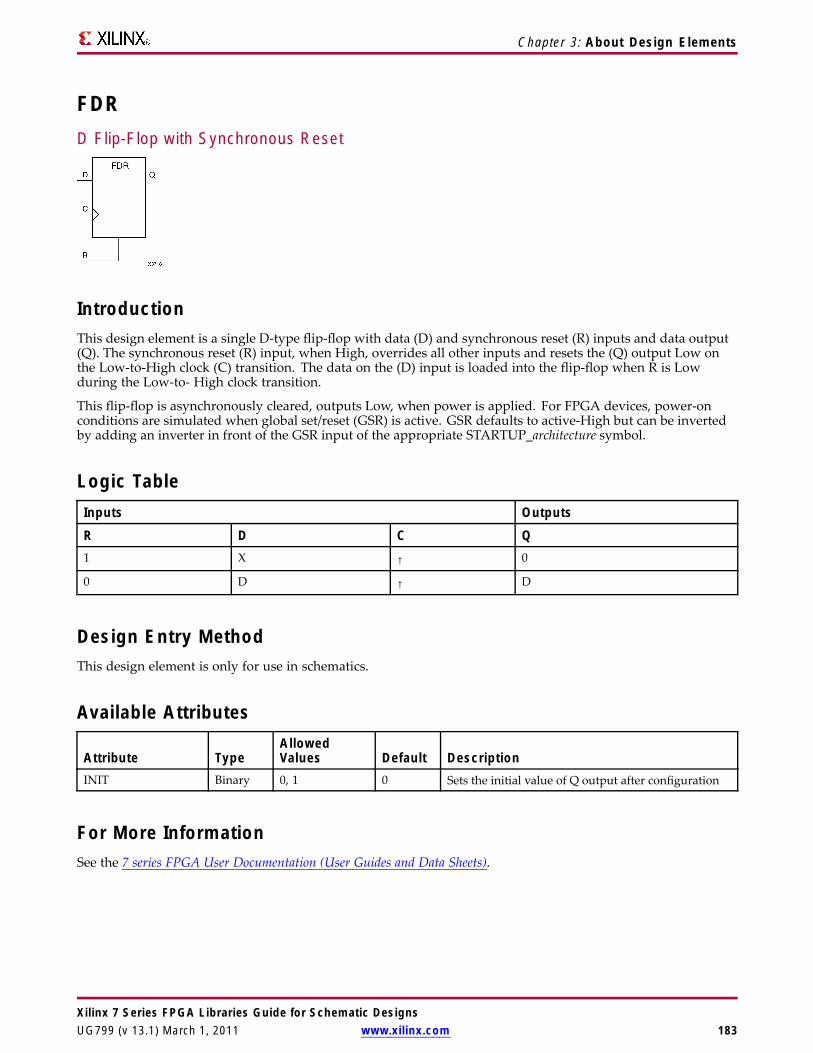
Chapter 3: About Design Elements
FDRD Flip-Flop with Synchronous Reset
IntroductionThis design element is a single D-type flip-flop with data (D) and synchronous reset (R) inputs and data output(Q). The synchronous reset (R) input, when High, overrides all other inputs and resets the (Q) output Low onthe Low-to-High clock (C) transition. The data on the (D) input is loaded into the flip-flop when R is Lowduring the Low-to- High clock transition.
This flip-flop is asynchronously cleared, outputs Low, when power is applied. For FPGA devices, power-onconditions are simulated when global set/reset (GSR) is active. GSR defaults to active-High but can be invertedby adding an inverter in front of the GSR input of the appropriate STARTUP_architecture symbol.
Logic TableInputs Outputs
R D C Q1 X ↑ 0
0 D ↑ D
Design Entry MethodThis design element is only for use in schematics.
Available Attributes
Attribute TypeAllowedValues Default Description
INIT Binary 0, 1 0 Sets the initial value of Q output after configuration
For More InformationSee the 7 series FPGA User Documentation (User Guides and Data Sheets).
Xilinx 7 Series FPGA Libraries Guide for Schematic DesignsUG799 (v 13.1) March 1, 2011 www.xilinx.com 183

Chapter 3: About Design Elements
FDR_1Primitive: D Flip-Flop with Negative-Edge Clock and Synchronous Reset
IntroductionThis design element is a single D-type flip-flop with data (D) and synchronous reset (R) inputs and data output(Q). The synchronous reset (R) input, when High, overrides all other inputs and resets the (Q) output Low onthe High-to-Low clock (C) transition. The data on the (D) input is loaded into the flip-flop when R is Lowduring the High-to- Low clock transition.
This flip-flop is asynchronously cleared, outputs Low, when power is applied. For FPGA devices, power-onconditions are simulated when global set/reset (GSR) is active. GSR defaults to active-High but can be invertedby adding an inverter in front of the GSR input of the appropriate STARTUP_architecture symbol.
Logic TableInputs Outputs
R D C Q1 X ↓ 0
0 D ↓ D
Design Entry MethodThis design element is only for use in schematics.
Available Attributes
Attribute TypeAllowedValues Default Description
INIT Binary 0, 1 0 Sets the initial value of Q output after configuration
For More InformationSee the 7 series FPGA User Documentation (User Guides and Data Sheets).
Xilinx 7 Series FPGA Libraries Guide for Schematic Designs184 www.xilinx.com UG799 (v 13.1) March 1, 2011

Chapter 3: About Design Elements
FDRED Flip-Flop with Clock Enable and Synchronous Reset
IntroductionThis design element is a single D-type flip-flop with data (D), clock enable (CE), and synchronous reset (R) inputsand data output (Q). The synchronous reset (R) input, when High, overrides all other inputs and resets the (Q)output Low on the Low-to-High clock (C) transition. The data on the (D) input is loaded into the flip-flop when Ris Low and CE is High during the Low-to-High clock transition.
This flip-flop is asynchronously cleared, outputs Low, when power is applied. For FPGA devices, power-onconditions are simulated when global set/reset (GSR) is active. GSR defaults to active-High but can be invertedby adding an inverter in front of the GSR input of the appropriate STARTUP_architecture symbol.
Logic TableInputs Outputs
R CE D C Q1 X X ↑ 0
0 0 X X No Change
0 1 D ↑ D
Design Entry MethodThis design element can be used in schematics.
Available Attributes
Attribute TypeAllowedValues Default Description
INIT Binary 0, 1 0 Sets the initial value of Q output after configuration
For More InformationSee the 7 series FPGA User Documentation (User Guides and Data Sheets).
Xilinx 7 Series FPGA Libraries Guide for Schematic DesignsUG799 (v 13.1) March 1, 2011 www.xilinx.com 185

Chapter 3: About Design Elements
FDRE_1Primitive: D Flip-Flop with Negative-Clock Edge, Clock Enable, and Synchronous Reset
IntroductionFDRE_1 is a single D-type flip-flop with data (D), clock enable (CE), and synchronous reset (R) inputs and dataoutput (Q). The synchronous reset (R) input, when High, overrides all other inputs and resets the (Q) output Lowon the High-to-Low clock (C) transition. The data on the (D) input is loaded into the flip-flop when R is Low andCE is High during the High-to-Low clock transition.
This flip-flop is asynchronously cleared, outputs Low, when power is applied. For FPGA devices, power-onconditions are simulated when global set/reset (GSR) is active. GSR defaults to active-High but can be invertedby adding an inverter in front of the GSR input of the appropriate STARTUP_architecture symbol.
Logic TableInputs Outputs
R CE D C Q1 X X ↓ 0
0 0 X X No Change
0 1 D ↓ D
Design Entry MethodThis design element is only for use in schematics.
Available Attributes
Attribute TypeAllowedValues Default Description
INIT Binary 0, 1 0 Sets the initial value of Q output after configuration
For Spartan®-6, the INIT value should always matchthe polarity of the set or reset. For this element, theINIT should be 0. If set to 1, an asynchronous circuitmust be created to exhibit this behavior, which Xilinxdoes not recommend.
For More InformationSee the 7 series FPGA User Documentation (User Guides and Data Sheets).
Xilinx 7 Series FPGA Libraries Guide for Schematic Designs186 www.xilinx.com UG799 (v 13.1) March 1, 2011

Chapter 3: About Design Elements
FDSD Flip-Flop with Synchronous Set
IntroductionFDS is a single D-type flip-flop with data (D) and synchronous set (S) inputs and data output (Q). Thesynchronous set input, when High, sets the Q output High on the Low-to-High clock (C) transition. The data onthe D input is loaded into the flip-flop when S is Low during the Low-to-High clock (C) transition.
For FPGA devices, this flip-flop is asynchronously preset, output High, when power is applied. Power-onconditions are simulated when global set/reset (GSR) is active. GSR defaults to active-High but can be invertedby adding an inverter in front of the GSR input of the appropriate STARTUP_architecture symbol.
Logic TableInputs Outputs
S D C Q1 X ↑ 1
0 D ↑ D
Design Entry MethodThis design element is only for use in schematics.
Available Attributes
Attribute TypeAllowedValues Default Description
INIT Binary 0, 1 1 Sets the initial value of Q output after configuration.
For More InformationSee the 7 series FPGA User Documentation (User Guides and Data Sheets).
Xilinx 7 Series FPGA Libraries Guide for Schematic DesignsUG799 (v 13.1) March 1, 2011 www.xilinx.com 187

Chapter 3: About Design Elements
FDS_1Primitive: D Flip-Flop with Negative-Edge Clock and Synchronous Set
IntroductionFDS is a single D-type flip-flop with data (D) and synchronous set (S) inputs and data output (Q). Thesynchronous set input, when High, sets the Q output High on the Low-to-High clock (C) transition. The data onthe D input is loaded into the flip-flop when S is Low during the Low-to-High clock (C) transition.
This flip-flop is asynchronously preset, output High, when power is applied. For FPGA devices, power-onconditions are simulated when global set/reset (GSR) is active. GSR defaults to active-High but can be invertedby adding an inverter in front of the GSR input of the appropriate STARTUP_architecture symbol.
Logic TableInputs Outputs
S D C Q1 X ↓ 1
0 D ↓ D
Design Entry MethodThis design element is only for use in schematics.
Available Attributes
Attribute TypeAllowedValues Default Description
INIT Binary 0, 1 1 Sets the initial value of Q output after configuration.
For More InformationSee the 7 series FPGA User Documentation (User Guides and Data Sheets).
Xilinx 7 Series FPGA Libraries Guide for Schematic Designs188 www.xilinx.com UG799 (v 13.1) March 1, 2011

Chapter 3: About Design Elements
FDSED Flip-Flop with Clock Enable and Synchronous Set
IntroductionFDSE is a single D-type flip-flop with data (D), clock enable (CE), and synchronous set (S) inputs and data output(Q). The synchronous set (S) input, when High, overrides the clock enable (CE) input and sets the Q output Highduring the Low-to-High clock (C) transition. The data on the D input is loaded into the flip-flop when S is Lowand CE is High during the Low-to-High clock (C) transition.
For FPGA devices, this flip-flop is asynchronously preset, output High, when power is applied. Power-onconditions are simulated when global set/reset (GSR) is active. GSR defaults to active-High but can be invertedby adding an inverter in front of the GSR input of the appropriate STARTUP_architecture symbol.
Logic TableInputs Outputs
S CE D C Q1 X X ↑ 1
0 0 X X No Change
0 1 D ↑ D
Design Entry MethodThis design element can be used in schematics.
Available Attributes
Attribute TypeAllowedValues Default Description
INIT Binary 0, 1 1 Sets the initial value of Q output after configuration
For More InformationSee the 7 series FPGA User Documentation (User Guides and Data Sheets).
Xilinx 7 Series FPGA Libraries Guide for Schematic DesignsUG799 (v 13.1) March 1, 2011 www.xilinx.com 189

Chapter 3: About Design Elements
FDSE_1Primitive: D Flip-Flop with Negative-Edge Clock, Clock Enable, and Synchronous Set
IntroductionFDSE_1 is a single D-type flip-flop with data (D), clock enable (CE), and synchronous set (S) inputs and dataoutput (Q). The synchronous set (S) input, when High, overrides the clock enable (CE) input and sets the Qoutput High during the High-to-Low clock (C) transition. The data on the D input is loaded into the flip-flopwhen S is Low and CE is High during the High-to-Low clock (C) transition.
This flip-flop is asynchronously preset, output High, when power is applied. For FPGA devices, power-onconditions are simulated when global set/reset (GSR) is active. GSR defaults to active-High but can be invertedby adding an inverter in front of the GSR input of the appropriate STARTUP_architecture symbol.
Logic TableInputs Outputs
S CE D C Q1 X X ↓ 1
0 0 X X No Change
0 1 D ↓ D
Design Entry MethodThis design element is only for use in schematics.
Available Attributes
Attribute TypeAllowedValues Default Description
INIT Binary 0, 1 1 Sets the initial value of Q output after configuration
For Spartan®-6, Xilinx recommends that the INITvalue always matches the polarity of the set or reset.For this element, the INIT should be 1. If set to 0,additional asynchronous circuitry will be created tocorrectly model the behavior.
For More InformationSee the 7 series FPGA User Documentation (User Guides and Data Sheets).
Xilinx 7 Series FPGA Libraries Guide for Schematic Designs190 www.xilinx.com UG799 (v 13.1) March 1, 2011

Chapter 3: About Design Elements
FIFO18E1Primitive: 18KB FIFO (First In, First Out) Block RAM Memory
Introduction7 series devices contain several block RAM memories, each of which can be separately configured as a FIFO, anautomatic error-correction RAM, or as a general-purpose 36KB or 18KB RAM/ROMmemory. These Block RAMmemories offer fast and flexible storage of large amounts of on-chip data. The FIFO18E1 uses the FIFO controllogic and the 18KB Block RAM. This primitive can be used in a 4-bit wide by 4K deep, 9-bit wide by 2K deep,18-bit wide by 1K deep, or a 36-bit wide by 512 deep configuration. The primitive can be configured in eithersynchronous or dual-clock (asynchronous) mode, with all associated FIFO flags and status signals. When usingthe dual-clock mode with independent clocks, depending on the offset between read and write clock edges, theEmpty, Almost Empty, Full and Almost Full flags can deassert one cycle later. Due to the asynchronous nature ofthe clocks the simulation model only reflects the deassertion latency cycles listed in the User Guide.
Note For a 36-bit wide by 512 deep FIFO, the FIFO18_36 mode must be used. For deeper or wider configurationsof the FIFO, the FIFO36E1 can be used. If error-correction circuitry is desired, the FIFO36E1 with FIFO36_72mode must be used.
Port DescriptionsPort Type Width FunctionALMOSTEMPTY Output 1 Programmable flag to indicate the FIFO is almost empty.
Synchronous to RDCLK. The offset for this flag is userconfigurable. ALMOST_EMPTY_OFFSET attributespecifies the threshold where this flag is triggered relativeto full/empty.
ALMOSTFULL Output 1 Programmable flag to indicate that the FIFO is almostfull. Synchronous to WRCLK. The offset for this flag isuser configurable. The ALMOST_FULL_OFFSET attributespecifies the threshold where this flag is triggered relativeto full/empty.
DI<31:0> Input 32 FIFO data input bus.
DIP<3:0> Input 4 FIFO parity data input bus.
DO<31:0> Output 32 FIFO data output bus.
Xilinx 7 Series FPGA Libraries Guide for Schematic DesignsUG799 (v 13.1) March 1, 2011 www.xilinx.com 191
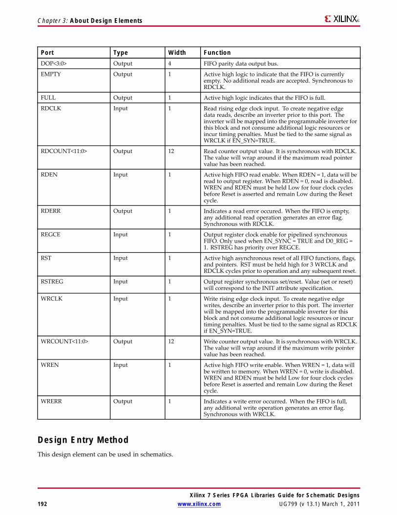
Chapter 3: About Design Elements
Port Type Width FunctionDOP<3:0> Output 4 FIFO parity data output bus.
EMPTY Output 1 Active high logic to indicate that the FIFO is currentlyempty. No additional reads are accepted. Synchronous toRDCLK.
FULL Output 1 Active high logic indicates that the FIFO is full.
RDCLK Input 1 Read rising edge clock input. To create negative edgedata reads, describe an inverter prior to this port. Theinverter will be mapped into the programmable inverter forthis block and not consume additional logic resources orincur timing penalties. Must be tied to the same signal asWRCLK if EN_SYN=TRUE.
RDCOUNT<11:0> Output 12 Read counter output value. It is synchronous with RDCLK.The value will wrap around if the maximum read pointervalue has been reached.
RDEN Input 1 Active high FIFO read enable. When RDEN = 1, data will beread to output register. When RDEN = 0, read is disabled.WREN and RDEN must be held Low for four clock cyclesbefore Reset is asserted and remain Low during the Resetcycle.
RDERR Output 1 Indicates a read error occured. When the FIFO is empty,any additional read operation generates an error flag.Synchronous with RDCLK.
REGCE Input 1 Output register clock enable for pipelined synchronousFIFO. Only used when EN_SYNC = TRUE and D0_REG =1. RSTREG has priority over REGCE.
RST Input 1 Active high asynchronous reset of all FIFO functions, flags,and pointers. RST must be held high for 3 WRCLK andRDCLK cycles prior to operation and any subsequent reset.
RSTREG Input 1 Output register synchronous set/reset. Value (set or reset)will correspond to the INIT attribute specification.
WRCLK Input 1 Write rising edge clock input. To create negative edgewrites, describe an inverter prior to this port. The inverterwill be mapped into the programmable inverter for thisblock and not consume additional logic resources or incurtiming penalties. Must be tied to the same signal as RDCLKif EN_SYN=TRUE.
WRCOUNT<11:0> Output 12 Write counter output value. It is synchronous withWRCLK.The value will wrap around if the maximum write pointervalue has been reached.
WREN Input 1 Active high FIFO write enable. When WREN = 1, data willbe written to memory. When WREN = 0, write is disabled.WREN and RDEN must be held Low for four clock cyclesbefore Reset is asserted and remain Low during the Resetcycle.
WRERR Output 1 Indicates a write error occurred. When the FIFO is full,any additional write operation generates an error flag.Synchronous with WRCLK.
Design Entry MethodThis design element can be used in schematics.
Xilinx 7 Series FPGA Libraries Guide for Schematic Designs192 www.xilinx.com UG799 (v 13.1) March 1, 2011

Chapter 3: About Design Elements
Available AttributesAttribute Type Allowed Values Default DescriptionALMOST_EMPTY_OFFSET
HEX 13’h0000 to13’h1fff
13’h0080 Specifies the amount of datacontents in the RAM to trigger theALMOST_EMPTY flag. Settingdetermines the difference betweenEMPTY and ALMOSTEMPTYconditions. Must be set usinghexadecimal notation.
ALMOST_FULL_OFFSET
HEX 13’h0000 to13’h1fff
13’h0080 Specifies the amount of datacontents in the RAM to triggerthe ALMOST_FULL flag. Settingdetermines the difference betweenFULL and ALMOSTFULL conditions.Must be set using hexadecimalnotation.
DATA_WIDTH DECIMAL 4, 9, 18, 36 4 Specifies the desired data width forthe FIFO.
DO_REG DECIMAL 1, 0 1 For dual-clock (asynchronous) FIFO,must be set to 1. For synchronousFIFO, DO_REG must be set to 0 forflags and data to follow a standardsynchronous FIFO operation. WhenDO_REG is set to 1, effectively apipeline register is added to the outputof the synchronous FIFO. Data thenhas a one clock cycle latency. However,the clock-to-out timing is improved.
EN_SYN BOOLEAN FALSE, TRUE FALSE EN_SYN denotes whether the FIFOis operating in either dual-clock (twoindependent clocks) or synchronous(a single clock) mode. If set to TRUE,must connect the same signal toWRCLK and RDCLK. If set to FALSE,must set DO_REG=1.
FIFO_MODE STRING FIFO18,FIFO18_36
FIFO18 Selects the FIFO regular or wide mode.Set to FIFO18 when data_width is setto 4, 9 or 18. Set to FIFO18_36 whenthe wide 36-bit data path is desired.
FIRST_WORD_FALL_THROUGH
BOOLEAN FALSE, TRUE FALSE If TRUE, the first write to the FIFOwill appear on DO without a RDENassertion.
INIT HEX 36 bit HEX 36’h000000000 Specifies the initial value on the DOoutput after configuration or GlobalSet/Reset (GSR).
SIM_DEVICE STRING “VIRTEX6”,“7SERIES”
“VIRTEX6” Must be set to "7SERIES" in order toexhibit proper simulation behaviorunder all conditions.
SRVAL HEX 36 bit HEX 36’h000000000 Specifies the output value of the FIFOupon assertion of the DO_REG reset(RSTREG) signal. Only supportedwhen DO_REG = 1 and EN_SYN =TRUE and RSTREG is connected to anactive signal.
Xilinx 7 Series FPGA Libraries Guide for Schematic DesignsUG799 (v 13.1) March 1, 2011 www.xilinx.com 193

Chapter 3: About Design Elements
For More InformationSee the 7 series FPGA User Documentation (User Guides and Data Sheets).
Xilinx 7 Series FPGA Libraries Guide for Schematic Designs194 www.xilinx.com UG799 (v 13.1) March 1, 2011
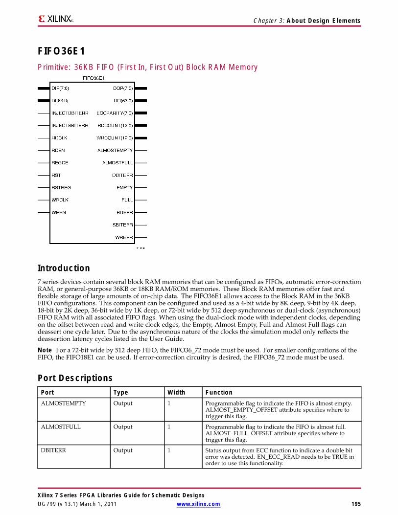
Chapter 3: About Design Elements
FIFO36E1Primitive: 36KB FIFO (First In, First Out) Block RAM Memory
Introduction7 series devices contain several block RAMmemories that can be configured as FIFOs, automatic error-correctionRAM, or general-purpose 36KB or 18KB RAM/ROM memories. These Block RAM memories offer fast andflexible storage of large amounts of on-chip data. The FIFO36E1 allows access to the Block RAM in the 36KBFIFO configurations. This component can be configured and used as a 4-bit wide by 8K deep, 9-bit by 4K deep,18-bit by 2K deep, 36-bit wide by 1K deep, or 72-bit wide by 512 deep synchronous or dual-clock (asynchronous)FIFO RAM with all associated FIFO flags. When using the dual-clock mode with independent clocks, dependingon the offset between read and write clock edges, the Empty, Almost Empty, Full and Almost Full flags candeassert one cycle later. Due to the asynchronous nature of the clocks the simulation model only reflects thedeassertion latency cycles listed in the User Guide.
Note For a 72-bit wide by 512 deep FIFO, the FIFO36_72 mode must be used. For smaller configurations of theFIFO, the FIFO18E1 can be used. If error-correction circuitry is desired, the FIFO36_72 mode must be used.
Port DescriptionsPort Type Width FunctionALMOSTEMPTY Output 1 Programmable flag to indicate the FIFO is almost empty.
ALMOST_EMPTY_OFFSET attribute specifies where totrigger this flag.
ALMOSTFULL Output 1 Programmable flag to indicate the FIFO is almost full.ALMOST_FULL_OFFSET attribute specifies where totrigger this flag.
DBITERR Output 1 Status output from ECC function to indicate a double biterror was detected. EN_ECC_READ needs to be TRUE inorder to use this functionality.
Xilinx 7 Series FPGA Libraries Guide for Schematic DesignsUG799 (v 13.1) March 1, 2011 www.xilinx.com 195

Chapter 3: About Design Elements
Port Type Width FunctionDI<63:0> Input 64 FIFO data input bus.
DIP<7:0> Input 8 FIFO parity data input bus.
DO<63:0> Output 64 FIFO data output bus.
DOP<7:0> Output 8 FIFO parity data output bus.
ECCPARITY<7:0> Output 8 ECC encoder data output bus for memory error detectionand correction.
EMPTY Output 1 Active high logic to indicate that the FIFO is currentlyempty. No additional reads are accepted. Synchronousto RDCLK.
FULL Output 1 Active high logic indicates that the FIFO is full (memory isfilled). No additional writes are accepted. Synchronous toWRCLK.
INJECTDBITERR Input 1 Inject a double bit error if ECC feature is used.
INJECTSBITERR Input 1 Inject single bit error if ECC is used. Creates a single biterror at a particular block RAM bit location when assertedduring write. The block RAM ECC logic corrects this errorwhen this location is read back. The error is created in bitDI[30].
RDCLK Input 1 Read rising edge clock input. To create negative edgedata reads, describe an inverter prior to this port. Theinverter will be mapped into the programmable inverterfor this block and not consume additional logic resourcesor incur timing penalties. Must be tied to the same signalas WRCLK if EN_SYN=TRUE.
RDCOUNT<12:0> Output 13 Read counter output value. It is synchronous with RDCLK.The value will wrap around if the maximum read pointervalue has been reached.
RDEN Input 1 Active high FIFO read enable. When RDEN = 1, datawill be read to output register. When RDEN = 0, read isdisabled. WREN and RDEN must be held Low for fourclock cycles before Reset is asserted and remain Lowduring the Reset cycle.
RDERR Output 1 Indicates a read error occured. When the FIFO is empty,any additional read operation generates an error flag.Synchronous with RDCLK.
REGCE Input 1 Output register clock enable for pipelined synchronousFIFO. Only used when EN_SYNC = TRUE and D0_REG =1. RSTREG has priority over REGCE.
RST Input 1 Active high (FIFO logic) asynchronous reset (for dual-clockFIFO), synchronous reset (synchronous FIFO) for 3 CLKcycles.
RSTREG Input 1 Output register synchronous set/reset. DO_REG must be 1to use this reset.
SBITERR Output 1 Status output from ECC function to indicate a single biterror was detected. EN_ECC_READ needs to be TRUE inorder to use this functionality.
Xilinx 7 Series FPGA Libraries Guide for Schematic Designs196 www.xilinx.com UG799 (v 13.1) March 1, 2011

Chapter 3: About Design Elements
Port Type Width FunctionWRCLK Input 1 Write rising edge clock input. To create negative edge
writes, describe an inverter prior to this port. The inverterwill be mapped into the programmable inverter for thisblock and not consume additional logic resources or incurtiming penalties. Must be tied to the same signal as RDCLKif EN_SYN=TRUE.
WRCOUNT<12:0> Output 13 Write counter output value. It is synchronous withWRCLK. The value will wrap around if the maximumwrite pointer value has been reached.
WREN Input 1 Active high FIFO write enable. When WREN = 1, data willbe written to memory. When WREN = 0, write is disabled.WREN and RDEN must be held Low for four clock cyclesbefore Reset is asserted and remain Low during the Resetcycle.
WRERR Output 1 Indicates a write error occured. When the FIFO is full,any additional write operation generates an error flag.Synchronous with WRCLK.
Design Entry MethodThis design element can be used in schematics.
Available AttributesAttribute Type Allowed Values Default DescriptionALMOST_EMPTY_OFFSET
HEX 13’h0000 to 13’h1fff 13’h0080 Specifies the amount of datacontents in the RAM to trigger theALMOST_EMPTY flag.
ALMOST_FULL_OFFSET
HEX 13’h0000 to 13’h1fff 13’h0080 Specifies the amount of datacontents in the RAM to trigger theALMOST_FULL flag.
DATA_WIDTH DECIMAL 4, 9, 18, 36, 72 4 Specifies the desired data widthfor the FIFO. For data widths of72, FIFO_MODE must be set to"FIFO36_72".
DO_REG DECIMAL 1, 0 1 Enable output register to the FIFO forimproved clock-to-out timing at theexpense of added read latency (onepipeline delay). DO_REG must be 1when EN_SYN is set to FALSE.
EN_ECC_READ BOOLEAN FALSE, TRUE FALSE Enable the ECC decoder circuitry.
EN_ECC_WRITE BOOLEAN FALSE, TRUE FALSE Enable the ECC encoder circuitry..
EN_SYN BOOLEAN FALSE, TRUE FALSE When FALSE, specifies the FIFO tobe used in asynchronous mode (twoindependent clock) or when TRUE insynchronous (a single clock) operation.
FIFO_MODE STRING “FIFO36”,“FIFO36_72”
FIFO36 Selects regular "FIFO36" or thewide "FIFO36_72" mode. If set to"FIFO36_72", the DATA_WIDTHattribute has to be 72.
FIRST_WORD_FALL_THROUGH
BOOLEAN FALSE, TRUE FALSE If TRUE, the first write to the FIFOwill appear on DO without a RDENassertion.
Xilinx 7 Series FPGA Libraries Guide for Schematic DesignsUG799 (v 13.1) March 1, 2011 www.xilinx.com 197

Chapter 3: About Design Elements
Attribute Type Allowed Values Default DescriptionINIT HEX 72 bit HEX all zeros Specifies the initial value on the DO
output after configuration.
SIM_DEVICE STRING “VIRTEX6”,“7SERIES”
“VIRTEX6” Must be set to "7SERIES" in order toexhibit proper simulation behaviorunder all conditions.
SRVAL HEX 72 bit HEX all zeros Specifies the output value of the FIFOupon assertion of the synchronousreset (RSTREG) signal. Only valid forDO_REG=1.
For More InformationSee the 7 series FPGA User Documentation (User Guides and Data Sheets).
Xilinx 7 Series FPGA Libraries Guide for Schematic Designs198 www.xilinx.com UG799 (v 13.1) March 1, 2011

Chapter 3: About Design Elements
FJKCMacro: J-K Flip-Flop with Asynchronous Clear
IntroductionThis design element is a single J-K-type flip-flop with J, K, and asynchronous clear (CLR) inputs and data output(Q). The asynchronous clear (CLR) input, when High, overrides all other inputs and resets the Q output Low.When CLR is Low, the output responds to the state of the J and K inputs, as shown in the following logictable, during the Low-to-High clock (C) transition.
This flip-flop is asynchronously cleared, outputs Low, when power is applied. For FPGA devices, power-onconditions are simulated when global set/reset (GSR) is active. GSR defaults to active-High but can be invertedby adding an inverter in front of the GSR input of the appropriate STARTUP_architecture symbol.
Logic TableInputs Outputs
CLR J K C Q1 X X X 0
0 0 0 ↑ No Change
0 0 1 ↑ 0
0 1 0 ↑ 1
0 1 1 ↑ Toggle
Design Entry MethodThis design element is only for use in schematics.
Available Attributes
Attribute TypeAllowedValues Default Description
INIT Binary 0, 1 0 Sets the initial value of Q output after configuration
For Spartan®-6, the INIT value should always matchthe polarity of the set or reset. For this element, theINIT should be 0. If set to 1, an asynchronous circuitmust be created to exhibit this behavior, which Xilinxdoes not recommend.
Xilinx 7 Series FPGA Libraries Guide for Schematic DesignsUG799 (v 13.1) March 1, 2011 www.xilinx.com 199

Chapter 3: About Design Elements
For More InformationSee the 7 series FPGA User Documentation (User Guides and Data Sheets).
Xilinx 7 Series FPGA Libraries Guide for Schematic Designs200 www.xilinx.com UG799 (v 13.1) March 1, 2011

Chapter 3: About Design Elements
FJKCEMacro: J-K Flip-Flop with Clock Enable and Asynchronous Clear
IntroductionThis design element is a single J-K-type flip-flop with J, K, clock enable (CE), and asynchronous clear (CLR)inputs and data output (Q). The asynchronous clear (CLR), when High, overrides all other inputs and resets theQ output Low. When CLR is Low and CE is High, Q responds to the state of the J and K inputs, as shown in thefollowing logic table, during the Low-to-High clock transition. When CE is Low, the clock transitions are ignored.
This flip-flop is asynchronously cleared, outputs Low, when power is applied. For FPGA devices, power-onconditions are simulated when global set/reset (GSR) is active. GSR defaults to active-High but can be invertedby adding an inverter in front of the GSR input of the appropriate STARTUP_architecture symbol.
Logic TableInputs Outputs
CLR CE J K C Q1 X X X X 0
0 0 X X X No Change
0 1 0 0 X No Change
0 1 0 1 ↑ 0
0 1 1 0 ↑ 1
0 1 1 1 ↑ Toggle
Design Entry MethodThis design element is only for use in schematics.
Available Attributes
Attribute TypeAllowedValues Default Description
INIT Binary 0, 1 0 Sets the initial value of Q output after configuration
For Spartan®-6, the INIT value should always matchthe polarity of the set or reset. For this element, theINIT should be 0. If set to 1, an asynchronous circuitmust be created to exhibit this behavior, which Xilinxdoes not recommend.
Xilinx 7 Series FPGA Libraries Guide for Schematic DesignsUG799 (v 13.1) March 1, 2011 www.xilinx.com 201

Chapter 3: About Design Elements
For More InformationSee the 7 series FPGA User Documentation (User Guides and Data Sheets).
Xilinx 7 Series FPGA Libraries Guide for Schematic Designs202 www.xilinx.com UG799 (v 13.1) March 1, 2011

Chapter 3: About Design Elements
FJKPMacro: J-K Flip-Flop with Asynchronous Preset
IntroductionThis design element is a single J-K-type flip-flop with J, K, and asynchronous preset (PRE) inputs and dataoutput (Q). The asynchronous preset (PRE) input, when High, overrides all other inputs and sets the (Q) outputHigh. When (PRE) is Low, the (Q) output responds to the state of the J and K inputs, as shown in the followinglogic table, during the Low-to-High clock transition.
For FPGA devices, this flip-flop is asynchronously preset, output High, when power is applied. Power-onconditions are simulated when global set/reset (GSR) is active. GSR defaults to active-High but can be invertedby adding an inverter in front of the GSR input of the appropriate STARTUP_architecture symbol.
Logic TableInputs Outputs
PRE J K C Q1 X X X 1
0 0 0 X No Change
0 0 1 ↑ 0
0 1 0 ↑ 1
0 1 1 ↑ Toggle
Design Entry MethodThis design element is only for use in schematics.
Available Attributes
Attribute TypeAllowedValues Default Description
INIT Binary 0, 1 1 Sets the initial value of Q output after configuration
For Spartan®-6, Xilinx recommends that the INITvalue always matches the polarity of the set or reset.For this element, the INIT should be 1. If set to 0,additional asynchronous circuitry will be created tocorrectly model the behavior.
Xilinx 7 Series FPGA Libraries Guide for Schematic DesignsUG799 (v 13.1) March 1, 2011 www.xilinx.com 203

Chapter 3: About Design Elements
For More InformationSee the 7 series FPGA User Documentation (User Guides and Data Sheets).
Xilinx 7 Series FPGA Libraries Guide for Schematic Designs204 www.xilinx.com UG799 (v 13.1) March 1, 2011

Chapter 3: About Design Elements
FJKPEMacro: J-K Flip-Flop with Clock Enable and Asynchronous Preset
IntroductionThis design element is a single J-K-type flip-flop with J, K, clock enable (CE), and asynchronous preset (PRE)inputs and data output (Q). The asynchronous preset (PRE), when High, overrides all other inputs and sets the(Q) output High. When (PRE) is Low and (CE) is High, the (Q) output responds to the state of the J and Kinputs, as shown in the logic table, during the Low-to-High clock (C) transition. When (CE) is Low, clocktransitions are ignored.
For FPGA devices, this flip-flop is asynchronously preset, output High, when power is applied. Power-onconditions are simulated when global set/reset (GSR) is active. GSR defaults to active-High but can be invertedby adding an inverter in front of the GSR input of the appropriate STARTUP_architecture symbol.
Logic TableInputs Outputs
PRE CE J K C Q1 X X X X 1
0 0 X X X No Change
0 1 0 0 X No Change
0 1 0 1 ↑ 0
0 1 1 0 ↑ 1
0 1 1 1 ↑ Toggle
Design Entry MethodThis design element is only for use in schematics.
Xilinx 7 Series FPGA Libraries Guide for Schematic DesignsUG799 (v 13.1) March 1, 2011 www.xilinx.com 205

Chapter 3: About Design Elements
Available Attributes
Attribute TypeAllowedValues Default Description
INIT Binary 0, 1 1 Sets the initial value of Q output after configuration
For Spartan®-6, Xilinx recommends that the INITvalue always matches the polarity of the set or reset.For this element, the INIT should be 1. If set to 0,additional asynchronous circuitry will be created tocorrectly model the behavior.
For More InformationSee the 7 series FPGA User Documentation (User Guides and Data Sheets).
Xilinx 7 Series FPGA Libraries Guide for Schematic Designs206 www.xilinx.com UG799 (v 13.1) March 1, 2011

Chapter 3: About Design Elements
FRAME_ECCE2Primitive: Configuration Frame Error Correction
IntroductionThis design element enables the dedicated, built-in error correction code (ECC) circuitry for the configurationmemory of the FPGA. This element contains outputs that allow monitoring of the status of the ECC circuitry andthe status of the readback CRC circuitry.
Port DescriptionsPort Type Width FunctionCRCERROR Output 1 Output indicating a CRC error.
ECCERROR Output 1 Output indicating an ECC error.
ECCERRORSINGLEOutput 1 Output Indicating single-bit Frame ECC error detected.
FAR<25:0> Output 26 Frame Address Register Value output.
SYNBIT<4:0> Output 5 Output bit address of error.
SYNDROME<12:0> Output 13 Output location of erroneous bit.
SYNDROMEVALIDOutput 1 Frame ECC output indicating the SYNDROME output is valid.
SYNWORD<6:0> Output 7 Word output in the frame where an ECC error has been detected.
Design Entry MethodThis design element can be used in schematics.
Available AttributesAttribute Type Allowed Values Default DescriptionFARSRC STRING EFAR, FAR EFAR Determines if the output of FAR[25:0]
configuration register points to the FARor EFAR. Sets configuration optionregister bit CTL0[7].
FRAME_RBT_IN_FILENAME
STRING 0 bit STRING NONE This file is output by the ICAP-E2model and it contains Frame Datainformation for the Raw Bitstream(RBT) file. The FRAME_ECCE2 modelwill parse this file, calculate ECC andoutput any error conditions.
Xilinx 7 Series FPGA Libraries Guide for Schematic DesignsUG799 (v 13.1) March 1, 2011 www.xilinx.com 207

Chapter 3: About Design Elements
For More InformationSee the 7 series FPGA User Documentation (User Guides and Data Sheets).
Xilinx 7 Series FPGA Libraries Guide for Schematic Designs208 www.xilinx.com UG799 (v 13.1) March 1, 2011

Chapter 3: About Design Elements
FTCMacro: Toggle Flip-Flop with Asynchronous Clear
IntroductionThis design element is a synchronous, resettable toggle flip-flop. The asynchronous clear (CLR) input, whenHigh, overrides all other inputs and resets the data output (Q) Low. The (Q) output toggles, or changes state,when the toggle enable (T) input is High and (CLR) is Low during the Low-to-High clock transition.
This flip-flop is asynchronously cleared, outputs Low, when power is applied. For FPGA devices, power-onconditions are simulated when global set/reset (GSR) is active. GSR defaults to active-High but can be invertedby adding an inverter in front of the GSR input of the appropriate STARTUP_architecture symbol.
Logic TableInputs Outputs
CLR T C Q1 X X 0
0 0 X No Change
0 1 ↑ Toggle
Design Entry MethodYou can instantiate this element when targeting a CPLD, but not when you are targeting an FPGA.
Available Attributes
Attribute TypeAllowedValues Default Description
INIT Binary 0, 1 0 Sets the initial value of Q output after configuration
For Spartan®-6, the INIT value should always matchthe polarity of the set or reset. For this element, theINIT should be 0. If set to 1, an asynchronous circuitmust be created to exhibit this behavior, which Xilinxdoes not recommend.
For More InformationSee the 7 series FPGA User Documentation (User Guides and Data Sheets).
Xilinx 7 Series FPGA Libraries Guide for Schematic DesignsUG799 (v 13.1) March 1, 2011 www.xilinx.com 209

Chapter 3: About Design Elements
FTCEMacro: Toggle Flip-Flop with Clock Enable and Asynchronous Clear
IntroductionThis design element is a toggle flip-flop with toggle and clock enable and asynchronous clear. When theasynchronous clear (CLR) input is High, all other inputs are ignored and the data output (Q) is reset Low. WhenCLR is Low and toggle enable (T) and clock enable (CE) are High, Q output toggles, or changes state, during theLow-to-High clock (C) transition. When CE is Low, clock transitions are ignored.
This flip-flop is asynchronously cleared, outputs Low, when power is applied. For FPGA devices, power-onconditions are simulated when global set/reset (GSR) is active. GSR defaults to active-High but can be invertedby adding an inverter in front of the GSR input of the appropriate STARTUP_architecture symbol.
Logic TableInputs Outputs
CLR CE T C Q1 X X X 0
0 0 X X No Change
0 1 0 X No Change
0 1 1 ↑ Toggle
Design Entry MethodThis design element is only for use in schematics.
Available Attributes
Attribute TypeAllowedValues Default Description
INIT Binary 0, 1 0 Sets the initial value of Q output after configuration
For Spartan®-6, the INIT value should always matchthe polarity of the set or reset. For this element, theINIT should be 0. If set to 1, an asynchronous circuitmust be created to exhibit this behavior, which Xilinxdoes not recommend.
For More InformationSee the 7 series FPGA User Documentation (User Guides and Data Sheets).
Xilinx 7 Series FPGA Libraries Guide for Schematic Designs210 www.xilinx.com UG799 (v 13.1) March 1, 2011

Chapter 3: About Design Elements
FTCLEMacro: Toggle/Loadable Flip-Flop with Clock Enable and Asynchronous Clear
IntroductionThis design element is a toggle/loadable flip-flop with toggle and clock enable and asynchronous clear. Whenthe asynchronous clear input (CLR) is High, all other inputs are ignored and output Q is reset Low. When loadenable input (L) is High and CLR is Low, clock enable (CE) is overridden and the data on data input (D) isloaded into the flip-flop during the Low-to-High clock (C) transition. When toggle enable (T) and CE are Highand L and CLR are Low, output Q toggles, or changes state, during the Low- to-High clock transition. WhenCE is Low, clock transitions are ignored.
This flip-flop is asynchronously cleared, outputs Low, when power is applied. For FPGA devices, power-onconditions are simulated when global set/reset (GSR) is active. GSR defaults to active-High but can be invertedby adding an inverter in front of the GSR input of the appropriate STARTUP_architecture symbol.
Logic TableInputs Outputs
CLR L CE T D C Q1 X X X X X 0
0 1 X X D ↑ D
0 0 0 X X X No Change
0 0 1 0 X X No Change
0 0 1 1 X ↑ Toggle
Design Entry MethodThis design element is only for use in schematics.
Available Attributes
Attribute TypeAllowedValues Default Description
INIT Binary 0, 1 0 Sets the initial value of Q output after configuration
For Spartan®-6, the INIT value should always matchthe polarity of the set or reset. For this element, theINIT should be 0. If set to 1, an asynchronous circuitmust be created to exhibit this behavior, which Xilinxdoes not recommend.
Xilinx 7 Series FPGA Libraries Guide for Schematic DesignsUG799 (v 13.1) March 1, 2011 www.xilinx.com 211

Chapter 3: About Design Elements
For More InformationSee the 7 series FPGA User Documentation (User Guides and Data Sheets).
Xilinx 7 Series FPGA Libraries Guide for Schematic Designs212 www.xilinx.com UG799 (v 13.1) March 1, 2011

Chapter 3: About Design Elements
FTCLEXMacro: Toggle/Loadable Flip-Flop with Clock Enable and Asynchronous Clear
IntroductionThis design element is a toggle/loadable flip-flop with toggle and clock enable and asynchronous clear. Whenthe asynchronous clear input (CLR) is High, all other inputs are ignored and output Q is reset Low. When loadenable input (L) is High, CLR is Low, and CE is High, the data on data input (D) is loaded into the flip-flop duringthe Low-to-High clock (C) transition. When toggle enable (T) and CE are High and L and CLR are Low, output Qtoggles, or changes state, during the Low- to-High clock transition. When CE is Low, clock transitions are ignored.
This flip-flop is asynchronously cleared, outputs Low, when power is applied. For FPGA devices, power-onconditions are simulated when global set/reset (GSR) is active. GSR defaults to active-High but can be invertedby adding an inverter in front of the GSR input of the appropriate STARTUP_architecture symbol.
Logic TableInputs Outputs
CLR L CE T D C Q1 X X X X X 0
0 1 X X D ↑ D
0 0 0 X X X No Change
0 0 1 0 X X No Change
0 0 1 1 X ↑ Toggle
Design Entry MethodThis design element is only for use in schematics.
Available Attributes
Attribute TypeAllowedValues Default Description
INIT Binary 0, 1 0 Sets the initial value of Q output after configuration
For Spartan®-6, the INIT value should always matchthe polarity of the set or reset. For this element, theINIT should be 0. If set to 1, an asynchronous circuitmust be created to exhibit this behavior, which Xilinxdoes not recommend.
Xilinx 7 Series FPGA Libraries Guide for Schematic DesignsUG799 (v 13.1) March 1, 2011 www.xilinx.com 213

Chapter 3: About Design Elements
For More InformationSee the 7 series FPGA User Documentation (User Guides and Data Sheets).
Xilinx 7 Series FPGA Libraries Guide for Schematic Designs214 www.xilinx.com UG799 (v 13.1) March 1, 2011

Chapter 3: About Design Elements
FTPMacro: Toggle Flip-Flop with Asynchronous Preset
IntroductionThis design element is a toggle flip-flop with toggle enable and asynchronous preset. When the asynchronouspreset (PRE) input is High, all other inputs are ignored and output (Q) is set High. When toggle-enable input (T)is High and (PRE) is Low, output (Q) toggles, or changes state, during the Low-to-High clock (C) transition.
For FPGA devices, this flip-flop is asynchronously preset, output High, when power is applied. Power-onconditions are simulated when global set/reset (GSR) is active. GSR defaults to active-High but can be invertedby adding an inverter in front of the GSR input of the appropriate STARTUP_architecture symbol.
Logic TableInputs Outputs
PRE T C Q1 X X 1
0 0 X No Change
0 1 ↑ Toggle
Design Entry MethodThis design element is only for use in schematics.
Available Attributes
Attribute TypeAllowedValues Default Description
INIT Binary 0, 1 1 Sets the initial value of Q output after configuration
For Spartan®-6, Xilinx recommends that the INITvalue always matches the polarity of the set or reset.For this element, the INIT should be 1. If set to 0,additional asynchronous circuitry will be created tocorrectly model the behavior.
For More InformationSee the 7 series FPGA User Documentation (User Guides and Data Sheets).
Xilinx 7 Series FPGA Libraries Guide for Schematic DesignsUG799 (v 13.1) March 1, 2011 www.xilinx.com 215

Chapter 3: About Design Elements
FTPEMacro: Toggle Flip-Flop with Clock Enable and Asynchronous Preset
IntroductionThis design element is a toggle flip-flop with toggle and clock enable and asynchronous preset. When theasynchronous preset (PRE) input is High, all other inputs are ignored and output (Q) is set High. When thetoggle enable input (T) is High, clock enable (CE) is High, and (PRE) is Low, output (Q) toggles, or changes state,during the Low-to-High clock transition. When (CE) is Low, clock transitions are ignored.
For FPGA devices, this flip-flop is asynchronously preset, output High, when power is applied. Power-onconditions are simulated when global set/reset (GSR) is active. GSR defaults to active-High but can be invertedby adding an inverter in front of the GSR input of the appropriate STARTUP_architecture symbol.
Logic TableInputs Outputs
PRE CE T C Q1 X X X 1
0 0 X X No Change
0 1 0 X No Change
0 1 1 ↑ Toggle
Design Entry MethodThis design element is only for use in schematics.
Available Attributes
Attribute TypeAllowedValues Default Description
INIT Binary 0, 1 1 Sets the initial value of Q output after configuration
For Spartan®-6, Xilinx recommends that the INITvalue always matches the polarity of the set or reset.For this element, the INIT should be 1. If set to 0,additional asynchronous circuitry will be created tocorrectly model the behavior.
For More InformationSee the 7 series FPGA User Documentation (User Guides and Data Sheets).
Xilinx 7 Series FPGA Libraries Guide for Schematic Designs216 www.xilinx.com UG799 (v 13.1) March 1, 2011

Chapter 3: About Design Elements
FTPLEMacro: Toggle/Loadable Flip-Flop with Clock Enable and Asynchronous Preset
IntroductionThis design element is a toggle/loadable flip-flop with toggle and clock enable and asynchronous preset. Whenthe asynchronous preset input (PRE) is High, all other inputs are ignored and output (Q) is set High. When theload enable input (L) is High and (PRE) is Low, the clock enable (CE) is overridden and the data (D) is loadedinto the flip-flop during the Low-to-High clock transition. When L and PRE are Low and toggle-enable input(T) and (CE) are High, output (Q) toggles, or changes state, during the Low-to-High clock transition. When(CE) is Low, clock transitions are ignored.
For FPGA devices, this flip-flop is asynchronously preset, output High, when power is applied. Power-onconditions are simulated when global set/reset (GSR) is active. GSR defaults to active-High but can be invertedby adding an inverter in front of the GSR input of the appropriate STARTUP_architecture symbol.
Logic TableInputs Outputs
PRE L CE T D C Q1 X X X X X 1
0 1 X X D ↑ D
0 0 0 X X X No Change
0 0 1 0 X X No Change
0 0 1 1 X ↑ Toggle
Design Entry MethodThis design element is only for use in schematics.
Xilinx 7 Series FPGA Libraries Guide for Schematic DesignsUG799 (v 13.1) March 1, 2011 www.xilinx.com 217

Chapter 3: About Design Elements
Available Attributes
Attribute TypeAllowedValues Default Description
INIT Binary 0, 1 1 Sets the initial value of Q output after configuration
For Spartan®-6, Xilinx recommends that the INITvalue always matches the polarity of the set or reset.For this element, the INIT should be 1. If set to 0,additional asynchronous circuitry will be created tocorrectly model the behavior.
For More InformationSee the 7 series FPGA User Documentation (User Guides and Data Sheets).
Xilinx 7 Series FPGA Libraries Guide for Schematic Designs218 www.xilinx.com UG799 (v 13.1) March 1, 2011

Chapter 3: About Design Elements
GNDPrimitive: Ground-Connection Signal Tag
IntroductionThe GND signal tag, or parameter, forces a net or input function to a Low logic level. A net tied to GND cannothave any other source.
When the logic-trimming software or fitter encounters a net or input function tied to GND, it removes any logicthat is disabled by the GND signal. The GND signal is only implemented when the disabled logic cannotbe removed.
Design Entry MethodThis design element is only for use in schematics.
For More InformationSee the 7 series FPGA User Documentation (User Guides and Data Sheets).
Xilinx 7 Series FPGA Libraries Guide for Schematic DesignsUG799 (v 13.1) March 1, 2011 www.xilinx.com 219
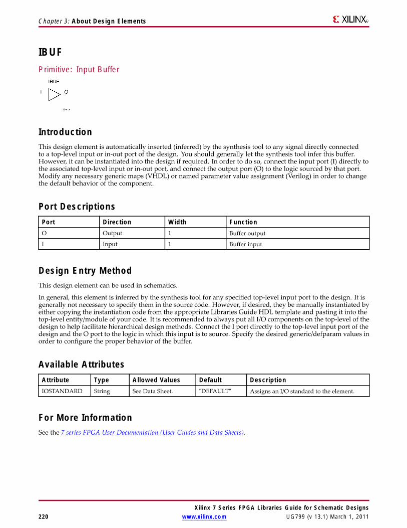
Chapter 3: About Design Elements
IBUFPrimitive: Input Buffer
IntroductionThis design element is automatically inserted (inferred) by the synthesis tool to any signal directly connectedto a top-level input or in-out port of the design. You should generally let the synthesis tool infer this buffer.However, it can be instantiated into the design if required. In order to do so, connect the input port (I) directly tothe associated top-level input or in-out port, and connect the output port (O) to the logic sourced by that port.Modify any necessary generic maps (VHDL) or named parameter value assignment (Verilog) in order to changethe default behavior of the component.
Port DescriptionsPort Direction Width FunctionO Output 1 Buffer output
I Input 1 Buffer input
Design Entry MethodThis design element can be used in schematics.
In general, this element is inferred by the synthesis tool for any specified top-level input port to the design. It isgenerally not necessary to specify them in the source code. However, if desired, they be manually instantiated byeither copying the instantiation code from the appropriate Libraries Guide HDL template and pasting it into thetop-level entity/module of your code. It is recommended to always put all I/O components on the top-level of thedesign to help facilitate hierarchical design methods. Connect the I port directly to the top-level input port of thedesign and the O port to the logic in which this input is to source. Specify the desired generic/defparam values inorder to configure the proper behavior of the buffer.
Available AttributesAttribute Type Allowed Values Default DescriptionIOSTANDARD String See Data Sheet. "DEFAULT" Assigns an I/O standard to the element.
For More InformationSee the 7 series FPGA User Documentation (User Guides and Data Sheets).
Xilinx 7 Series FPGA Libraries Guide for Schematic Designs220 www.xilinx.com UG799 (v 13.1) March 1, 2011

Chapter 3: About Design Elements
IBUF16Macro: 16-Bit Input Buffer
IntroductionInput Buffers isolate the internal circuit from the signals coming into the chip. This design element is containedin input/output blocks (IOBs) and allows the specification of the particular I/O Standard to configure the I/O. Ingeneral, an this element should be used for all single-ended data input or bidirectional pins.
Design Entry MethodThis design element can be used in schematics.
This element is usually inferred by the synthesis tool for any specified top-level input port to the design, andtherefore it is generally not necessary to specify the element in source code. However, if desired, this elementmay be manually instantiated by copying the instantiation code from below and pasting it into the top-levelentity/module of your code. Xilinx recommends that you put all I/O components on the top-level of the design tohelp facilitate hierarchical design methods. Connect the I port directly to the top-level input port of the designand the O port to the logic in which this input is to source. Specify the desired generic/defparam values inorder to configure the proper behavior of the buffer.
Available AttributesAttribute Type Allowed Values Default DescriptionIOSTANDARD String See Data Sheet. "DEFAULT" Assigns an I/O standard to the element.
For More InformationSee the 7 series FPGA User Documentation (User Guides and Data Sheets).
Xilinx 7 Series FPGA Libraries Guide for Schematic DesignsUG799 (v 13.1) March 1, 2011 www.xilinx.com 221

Chapter 3: About Design Elements
IBUF4Macro: 4-Bit Input Buffer
IntroductionInput Buffers isolate the internal circuit from the signals coming into the chip. This design element is containedin input/output blocks (IOBs) and allows the specification of the particular I/O Standard to configure the I/O. Ingeneral, an this element should be used for all single-ended data input or bidirectional pins.
Design Entry MethodThis design element can be used in schematics.
This element is usually inferred by the synthesis tool for any specified top-level input port to the design, andtherefore it is generally not necessary to specify the element in source code. However, if desired, this elementmay be manually instantiated by copying the instantiation code from below and pasting it into the top-levelentity/module of your code. Xilinx recommends that you put all I/O components on the top-level of the design tohelp facilitate hierarchical design methods. Connect the I port directly to the top-level input port of the designand the O port to the logic in which this input is to source. Specify the desired generic/defparam values inorder to configure the proper behavior of the buffer.
Available AttributesAttribute Type Allowed Values Default DescriptionIOSTANDARD String See Data Sheet. "DEFAULT" Assigns an I/O standard to the element.
For More InformationSee the 7 series FPGA User Documentation (User Guides and Data Sheets).
Xilinx 7 Series FPGA Libraries Guide for Schematic Designs222 www.xilinx.com UG799 (v 13.1) March 1, 2011

Chapter 3: About Design Elements
IBUF8Macro: 8-Bit Input Buffer
IntroductionInput Buffers isolate the internal circuit from the signals coming into the chip. This design element is containedin input/output blocks (IOBs) and allows the specification of the particular I/O Standard to configure the I/O. Ingeneral, an this element should be used for all single-ended data input or bidirectional pins.
Design Entry MethodThis design element can be used in schematics.
This element is usually inferred by the synthesis tool for any specified top-level input port to the design, andtherefore it is generally not necessary to specify the element in source code. However, if desired, this elementmay be manually instantiated by copying the instantiation code from below and pasting it into the top-levelentity/module of your code. Xilinx recommends that you put all I/O components on the top-level of the design tohelp facilitate hierarchical design methods. Connect the I port directly to the top-level input port of the designand the O port to the logic in which this input is to source. Specify the desired generic/defparam values inorder to configure the proper behavior of the buffer.
Available AttributesAttribute Type Allowed Values Default DescriptionIOSTANDARD String See Data Sheet. "DEFAULT" Assigns an I/O standard to the element.
For More InformationSee the 7 series FPGA User Documentation (User Guides and Data Sheets).
Xilinx 7 Series FPGA Libraries Guide for Schematic DesignsUG799 (v 13.1) March 1, 2011 www.xilinx.com 223

Chapter 3: About Design Elements
IBUFDSPrimitive: Differential Signaling Input Buffer
IntroductionThis design element is an input buffer that supports low-voltage, differential signaling. In IBUFDS, a designlevel interface signal is represented as two distinct ports (I and IB), one deemed the "master" and the other the"slave." The master and the slave are opposite phases of the same logical signal (for example, MYNET_P andMYNET_N). Optionally, a programmable differential termination feature is available to help improve signalintegrity and reduce external components.
Logic TableInputs Outputs
I IB O0 0 No Change
0 1 0
1 0 1
1 1 No Change
Port DescriptionsPort Type Width FunctionI Input 1 Diff_p Buffer Input
IB Input 1 Diff_n Buffer Input
O Output 1 Buffer Output
Design Entry MethodThis design element can be used in schematics.
Put all I/O components on the top-level of the design to help facilitate hierarchical design methods. Connectthe I port directly to the top-level "master" input port of the design, the IB port to the top-level "slave" inputport, and the O port to the logic in which this input is to source. Specify the desired generic/defparam values inorder to configure the proper behavior of the buffer.
Available Attributes
Attribute TypeAllowedValues Default Description
IOSTANDARD String See Data Sheet. "DEFAULT" Assigns an I/O standard to the element.
For More InformationSee the 7 series FPGA User Documentation (User Guides and Data Sheets).
Xilinx 7 Series FPGA Libraries Guide for Schematic Designs224 www.xilinx.com UG799 (v 13.1) March 1, 2011

Chapter 3: About Design Elements
IBUFDS_DIFF_OUTPrimitive: 7 series JTAG Boundary Scan Logic Control Circuit
IntroductionThis design element allows access to and from internal logic by the JTAG Boundary Scan logic controller. Thisallows for communication between the internal running design and the dedicated JTAG pins of the FPGA.
Port DescriptionsPort Type Width FunctionCAPTURE Output 1 CAPTURE output from TAP controller.
DRCK Output 1 Data register output for USER functions.
Design Entry MethodThis design element can be used in schematics.
Available AttributesAttribute Type Allowed Values Default DescriptionDDR_CLK_EDGE String "OPPOSITE_EDGE",
"SAME_EDGE""OPPOSITE_EDGE" DDR clock mode recovery mode
selection.
INIT Integer 0, 1 1 Q initialization value.
SRTYPE String "SYNC", "ASYNC" "SYNC" Set/Reset type selection.
For More Information• See the 7 series FPGA SelectIO Resources User Guide.
• See the 7 series FPGA Data Sheet DC and Switching Characteristics.
Xilinx 7 Series FPGA Libraries Guide for Schematic DesignsUG799 (v 13.1) March 1, 2011 www.xilinx.com 225

Chapter 3: About Design Elements
IBUFGPrimitive: Dedicated Input Clock Buffer
IntroductionThe IBUFG is a dedicated input to the device that should be used to connect incoming clocks to the FPGA’s globalclock routing resources. The IBUFG provides dedicated connections from a top level port to the MMCM or BUFGproviding the minimum amount of clock delay and jitter to the device. The IBUFG input can only be drivenby the clock capable (CC) or global clock (GC) pins. The IBUFG provides dedicated connections to the DCM,PLL, or BUFG resources. providing the minimum amount of clock delay and jitter to the device. The IBUFGinput can only be driven by the global clock (GC) pins.
Port DescriptionsPort Direction Width FunctionO Output 1 Clock Buffer output.
I Input 1 Clock Buffer input.
Design Entry MethodThis design element can be used in schematics.
Available AttributesAttribute Type Allowed Values Default DescriptionIOSTANDARD String See Data Sheet "DEFAULT" Assigns an I/O standard to the
element.
For More InformationSee the 7 series FPGA User Documentation (User Guides and Data Sheets).
Xilinx 7 Series FPGA Libraries Guide for Schematic Designs226 www.xilinx.com UG799 (v 13.1) March 1, 2011

Chapter 3: About Design Elements
IBUFGDSPrimitive: Differential Signaling Dedicated Input Clock Buffer and Optional Delay
IntroductionThis design element is a dedicated differential signaling input buffer for connection to the clock buffer (BUFG) orMMCM. In IBUFGDS, a design-level interface signal is represented as two distinct ports (I and IB), one deemedthe "master" and the other the "slave." The master and the slave are opposite phases of the same logical signal (forexample, MYNET_P and MYNET_N). Optionally, a programmable differential termination feature is available tohelp improve signal integrity and reduce external components. Also available is a programmable delay is toassist in the capturing of incoming data to the device.
Logic TableInputs Outputs
I IB O0 0 No Change
0 1 0
1 0 1
1 1 No Change
Port DescriptionsPort Direction Width FunctionO Output 1 Clock Buffer output
IB Input 1 Diff_n Clock Buffer Input
I Input 1 Diff_p Clock Buffer Input
Design Entry MethodThis design element can be used in schematics.
Put all I/O components on the top-level of the design to help facilitate hierarchical design methods. Connect the Iport directly to the top-level "master" input port of the design, the IB port to the top-level "slave" input port andthe O port to an MMCM, BUFG or logic in which this input is to source. Some synthesis tools infer the BUFGautomatically if necessary, when connecting an IBUFG to the clock resources of the FPGA. Specify the desiredgeneric/defparam values in order to configure the proper behavior of the buffer.
Available Attributes
Attribute TypeAllowedValues Default Description
IOSTANDARD String See Data Sheet "DEFAULT" Assigns an I/O standard to theelement.
Xilinx 7 Series FPGA Libraries Guide for Schematic DesignsUG799 (v 13.1) March 1, 2011 www.xilinx.com 227

Chapter 3: About Design Elements
For More InformationSee the 7 series FPGA User Documentation (User Guides and Data Sheets).
Xilinx 7 Series FPGA Libraries Guide for Schematic Designs228 www.xilinx.com UG799 (v 13.1) March 1, 2011

Chapter 3: About Design Elements
IBUFGDS_DIFF_OUTPrimitive: Differential Signaling Input Buffer with Differential Output
IntroductionThis design element is an input buffer that supports differential signaling. In IBUFDS_DIFF_OUT, a designlevel interface signal is represented as two distinct ports (I and IB), one deemed the "master" and the other the"slave." The master and the slave are opposite phases of the same logical signal (for example, MYNET_P andMYNET_N). The IBUFDS_DIFF_OUT differs from the IBUFDS in that it allows internal access to both phases ofthe differential signal. Optionally, a programmable differential termination feature is available to help improvesignal integrity and reduce external components.
Logic TableInputs Outputs
I IB O OB0 0 No Change No Change
0 1 0 1
1 0 1 0
1 1 No Change No Change
Port DescriptionsPort Direction Width FunctionI Input 1 Diff_p Buffer Input (connect to top-level port in the design).
IB Input 1 Diff_n Buffer Input (connect to top-level port in the design).
O Output 1 Diff_p Buffer Output.
OB Output 1 Diff_n Buffer Output.
Design Entry MethodXilinx suggests that you put all I/O components on the top-level of the design to help facilitate hierarchicaldesign methods. Connect the I port directly to the top-level "master" input port of the design, the IB port to thetop-level "slave" input port, and the O and OB ports to the logic in which this input is to source. Specify thedesired generic/parameter values in order to configure the proper behavior of the buffer.
Available AttributesAttribute Type Allowed Values Default DescriptionIOSTANDARD String See Data Sheet "DEFAULT" Assigns an I/O standard to the element.
DIFF_TERM Boolean TRUE, FALSE FALSE Specifies the use of the internal differentialtermination resistance.
Xilinx 7 Series FPGA Libraries Guide for Schematic DesignsUG799 (v 13.1) March 1, 2011 www.xilinx.com 229

Chapter 3: About Design Elements
For More Information• See the 7 series FPGA SelectIO Resources User Guide.
• See the 7 series FPGA User Documentation (User Guides and Data Sheets).
Xilinx 7 Series FPGA Libraries Guide for Schematic Designs230 www.xilinx.com UG799 (v 13.1) March 1, 2011

Chapter 3: About Design Elements
ICAPE2Primitive: Internal Configuration Access Port
IntroductionThis design element gives you access to the configuration functions of the FPGA from the FPGA fabric. Usingthis component, commands and data can be written to and read from the configuration logic of the FPGA array.Since the improper use of this function can have a negative effect on the functionality and reliability of the FPGA,you should not use this element unless you are very familiar with its capabilities.
Port DescriptionsPort Type Width FunctionCLK Input 1 Clock Input.
CSIB Input 1 Active-Low ICAP Enable.
I<31:0> Input 32 Configuration data input bus.
O<31:0> Output 32 Configuration data output bus.
RDWRB Input 1 Read/Write Select input.
Design Entry MethodThis design element can be used in schematics.
Available AttributesAttribute Type Allowed Values Default DescriptionDEVICE_ID HEX Any 32-bit hex value. 32’h00000000 Must specify the 32-bit value that
matches the pre-programmed DeviceID value.
ICAP_WIDTH STRING X32, X8, X16 X32 Specifies the input and output datawidth to be used with the ICAPE2.Possible values: (X8,X16 or X32)
SIM_CFG_FILE_NAME
STRING 0 bit STRING NONE Specifies the Raw Bitstream (RBT) fileto be parsed by the simulation model
For More InformationSee the 7 series FPGA User Documentation (User Guides and Data Sheets).
Xilinx 7 Series FPGA Libraries Guide for Schematic DesignsUG799 (v 13.1) March 1, 2011 www.xilinx.com 231

Chapter 3: About Design Elements
IDDRPrimitive: Input Dual Data-Rate Register
IntroductionThis design element is a dedicated input register designed to receive external dual data rate (DDR) signals intoXilinx® FPGAs. The IDDR is available with modes that present the data to the FPGA fabric at the time andclock edge they are captured, or on the same clock edge. This feature allows you to avoid additional timingcomplexities and resource usage.• OPPOSITE_EDGE mode - Data is recovered in the classic DDR methodology. Given a DDR data and
clock at pin D and C respectively, Q1 changes after every positive edge of clock C, and Q2 changes afterevery negative edge of clock C.
• SAME_EDGEmode -Data is still recovered by opposite edges of clock C. However, an extra register has beenplaced in front of the negative edge data register. This extra register is clocked with positive clock edge ofclock signal C. As a result, DDR data is now presented into the FPGA fabric at the same clock edge. However,because of this feature, the data pair appears to be "separated." Q1 and Q2 no longer have pair 1 and 2.Instead, the first pair presented is Pair 1 and DONT_CARE, followed by Pair 2 and 3 at the next clock cycle.
• SAME_EDGE_PIPELINED mode - Recovers data in a similar fashion as the SAME_EDGE mode. In orderto avoid the "separated" effect of the SAME_EDGE mode, an extra register has been placed in front of thepositive edge data register. A data pair now appears at the Q1 and Q2 pin at the same time. However, usingthis mode costs you an additional cycle of latency for Q1 and Q2 signals to change.
IDDR also works with the SelectIO™ features, such as the IODELAY.
Note For high speed interfaces, the IDDR_2CLK component can be used to specify two independent clocksto capture the data. Use this component when the performance requirements of the IDDR are not adequate,since the IDDR_2CLK requires more clocking resources and can imply placement restrictions that are notnecessary when using the IDDR component.
Port DescriptionsPort Direction Width FunctionQ1 - Q2 Output 1 These pins are the IDDR output that connects to the FPGA fabric. Q1 is
the first data pair and Q2 is the second data pair.
C Input 1 Clock input pin.
CE Input 1 When asserted Low, this port disables the output clock at port O.
D Input 1 This pin is where the DDR data is presented into the IDDR module.
This pin connects to a top-level input or bi-directional port, andIODELAY configured for an input delay or to an appropriate input orbidirectional buffer.
R Input 1 Active high reset forcing Q1 and Q2 to a logic zero. Can be synchronousor asynchronous based on the SRTYPE attribute.
S Input 1 Active high reset forcing Q1 and Q2 to a logic one. Can be synchronousor asynchronous based on the SRTYPE attribute.
Xilinx 7 Series FPGA Libraries Guide for Schematic Designs232 www.xilinx.com UG799 (v 13.1) March 1, 2011

Chapter 3: About Design Elements
Design Entry MethodThis design element can be used in schematics.
Available AttributesAttribute Type Allowed Values Default DescriptionDDR_CLK_EDGE String "OPPOSITE_EDGE",
"SAME_EDGE","SAME_EDGE_PIPELINED"
"OPPOSITE_EDGE”
Sets the IDDR mode of operation withrespect to clock edge.
INIT_Q1 Binary 0, 1 0 Initial value on the Q1 pin afterconfiguration startup or when GSR isasserted.
INIT_Q2 Binary 0, 1 0 Initial value on the Q2 pin afterconfiguration startup or when GSR isasserted.
SRTYPE String "SYNC" or "ASYNC” "SYNC” Set/reset type selection. "SYNC" specifiesthe behavior of the reset (R) and set (S)pins to be synchronous to the positive edgeof the C clock pin. "ASYNC" specifies anasynchronous set/reset function.
For More InformationSee the 7 series FPGA User Documentation (User Guides and Data Sheets).
Xilinx 7 Series FPGA Libraries Guide for Schematic DesignsUG799 (v 13.1) March 1, 2011 www.xilinx.com 233
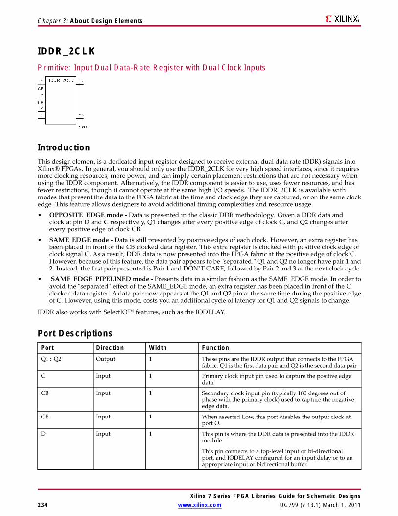
Chapter 3: About Design Elements
IDDR_2CLKPrimitive: Input Dual Data-Rate Register with Dual Clock Inputs
IntroductionThis design element is a dedicated input register designed to receive external dual data rate (DDR) signals intoXilinx® FPGAs. In general, you should only use the IDDR_2CLK for very high speed interfaces, since it requiresmore clocking resources, more power, and can imply certain placement restrictions that are not necessary whenusing the IDDR component. Alternatively, the IDDR component is easier to use, uses fewer resources, and hasfewer restrictions, though it cannot operate at the same high I/O speeds. The IDDR_2CLK is available withmodes that present the data to the FPGA fabric at the time and clock edge they are captured, or on the same clockedge. This feature allows designers to avoid additional timing complexities and resource usage.• OPPOSITE_EDGE mode - Data is presented in the classic DDR methodology. Given a DDR data and
clock at pin D and C respectively, Q1 changes after every positive edge of clock C, and Q2 changes afterevery positive edge of clock CB.
• SAME_EDGE mode - Data is still presented by positive edges of each clock. However, an extra register hasbeen placed in front of the CB clocked data register. This extra register is clocked with positive clock edge ofclock signal C. As a result, DDR data is now presented into the FPGA fabric at the positive edge of clock C.However, because of this feature, the data pair appears to be "separated." Q1 and Q2 no longer have pair 1 and2. Instead, the first pair presented is Pair 1 and DON’T CARE, followed by Pair 2 and 3 at the next clock cycle.
• SAME_EDGE_PIPELINED mode - Presents data in a similar fashion as the SAME_EDGE mode. In order toavoid the "separated" effect of the SAME_EDGE mode, an extra register has been placed in front of the Cclocked data register. A data pair now appears at the Q1 and Q2 pin at the same time during the positive edgeof C. However, using this mode, costs you an additional cycle of latency for Q1 and Q2 signals to change.
IDDR also works with SelectIO™ features, such as the IODELAY.
Port DescriptionsPort Direction Width FunctionQ1 : Q2 Output 1 These pins are the IDDR output that connects to the FPGA
fabric. Q1 is the first data pair and Q2 is the second data pair.
C Input 1 Primary clock input pin used to capture the positive edgedata.
CB Input 1 Secondary clock input pin (typically 180 degrees out ofphase with the primary clock) used to capture the negativeedge data.
CE Input 1 When asserted Low, this port disables the output clock atport O.
D Input 1 This pin is where the DDR data is presented into the IDDRmodule.
This pin connects to a top-level input or bi-directionalport, and IODELAY configured for an input delay or to anappropriate input or bidirectional buffer.
Xilinx 7 Series FPGA Libraries Guide for Schematic Designs234 www.xilinx.com UG799 (v 13.1) March 1, 2011

Chapter 3: About Design Elements
Port Direction Width FunctionR Input 1 Active high reset forcing Q1 and Q2 to a logic zero. Can
be synchronous or asynchronous based on the SRTYPEattribute.
S Input 1 Active high reset forcing Q1 and Q2 to a logic one. Canbe synchronous or asynchronous based on the SRTYPEattribute.
Design Entry MethodThis design element can be used in schematics.
• Connect the C pin to the appropriate clock source, representing the positive clock edge and CB to theclock source representing the negative clock edge.
• Connect the D pin to the top-level input, or bidirectional port, an IODELAY, or an instantiated inputor bidirectional buffer.
• The Q1 and Q2 pins should be connected to the appropriate data sources.
• CE should be tied high when not used, or connected to the appropriate clock enable logic.
• R and S pins should be tied low, if not used, or to the appropriate set or reset generation logic.
• Set all attributes to the component to represent the desired behavior.
• Always instantiate this component in pairs with the same clocking, and to LOC those to the appropriate Pand N I/O pair in order not to sacrifice possible I/O resources.
• Always instantiate this component in the top-level hierarchy of your design, along with any otherinstantiated I/O components for the design. This helps facilitate hierarchical design flows/practices.
• To minimize CLK skew, both CLK and CLKB should come from global routing (DCM / MMCM) and notfrom the local inversion. DCM / MMCM de-skews these clocks whereas the local inversion adds skew.
Available AttributesAttribute Type Allowed Values Default DescriptionDDR_CLK_EDGE String "OPPOSITE_EDGE",
"SAME_EDGE""SAME_EDGE_PIPELINED"
"OPPOSITE_EDGE”
DDR clock mode recovery modeselection. See Introduction for moreexplanation.
INIT_Q1 Binary 0, 1 0 Initial value on the Q1 pin afterconfiguration startup or when GSR isasserted.
INIT_Q2 Binary 0, 1 0 Initial value on the Q2 pin afterconfiguration startup or when GSR isasserted.
SRTYPE String "SYNC" or "ASYNC” "SYNC” Set/reset type selection. SYNC"specifies the behavior of the reset (R)and set (S) pins to be synchronous tothe positive edge of the C clock pin."ASYNC" specifies an asynchronousset/reset function.
Xilinx 7 Series FPGA Libraries Guide for Schematic DesignsUG799 (v 13.1) March 1, 2011 www.xilinx.com 235
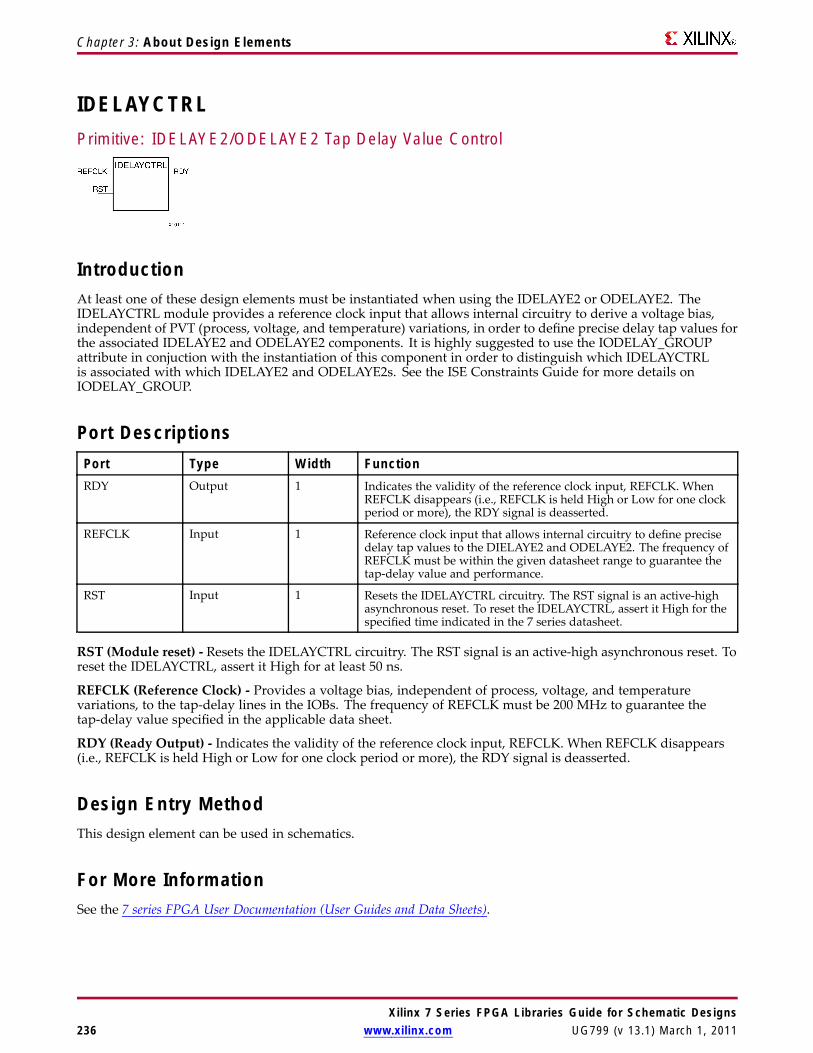
Chapter 3: About Design Elements
IDELAYCTRLPrimitive: IDELAYE2/ODELAYE2 Tap Delay Value Control
IntroductionAt least one of these design elements must be instantiated when using the IDELAYE2 or ODELAYE2. TheIDELAYCTRL module provides a reference clock input that allows internal circuitry to derive a voltage bias,independent of PVT (process, voltage, and temperature) variations, in order to define precise delay tap values forthe associated IDELAYE2 and ODELAYE2 components. It is highly suggested to use the IODELAY_GROUPattribute in conjuction with the instantiation of this component in order to distinguish which IDELAYCTRLis associated with which IDELAYE2 and ODELAYE2s. See the ISE Constraints Guide for more details onIODELAY_GROUP.
Port DescriptionsPort Type Width FunctionRDY Output 1 Indicates the validity of the reference clock input, REFCLK. When
REFCLK disappears (i.e., REFCLK is held High or Low for one clockperiod or more), the RDY signal is deasserted.
REFCLK Input 1 Reference clock input that allows internal circuitry to define precisedelay tap values to the DIELAYE2 and ODELAYE2. The frequency ofREFCLK must be within the given datasheet range to guarantee thetap-delay value and performance.
RST Input 1 Resets the IDELAYCTRL circuitry. The RST signal is an active-highasynchronous reset. To reset the IDELAYCTRL, assert it High for thespecified time indicated in the 7 series datasheet.
RST (Module reset) - Resets the IDELAYCTRL circuitry. The RST signal is an active-high asynchronous reset. Toreset the IDELAYCTRL, assert it High for at least 50 ns.
REFCLK (Reference Clock) - Provides a voltage bias, independent of process, voltage, and temperaturevariations, to the tap-delay lines in the IOBs. The frequency of REFCLK must be 200 MHz to guarantee thetap-delay value specified in the applicable data sheet.
RDY (Ready Output) - Indicates the validity of the reference clock input, REFCLK. When REFCLK disappears(i.e., REFCLK is held High or Low for one clock period or more), the RDY signal is deasserted.
Design Entry MethodThis design element can be used in schematics.
For More InformationSee the 7 series FPGA User Documentation (User Guides and Data Sheets).
Xilinx 7 Series FPGA Libraries Guide for Schematic Designs236 www.xilinx.com UG799 (v 13.1) March 1, 2011

Chapter 3: About Design Elements
IDELAYE2Primitive: Input Fixed or Variable Delay Element
IntroductionEvery I/O block contains a programmable absolute delay element called IDELAYE2. The IDELAYE2 can beconnected to an input register/ISERDESE1 or driven directly into FPGA logic. The IDELAYE2 is a 32-tap,wraparound, delay element with a calibrated tap resolution. Refer to the 7 series FPGA Data Sheet for delayvalues. The IDELAYE2 allows incoming signals to be delayed on an individual basis. The tap delay resolution isvaried by selecting an IDELAYCTRL reference clock from the range specified in the 7 series FPGA Data Sheet.
Design Entry MethodThis design element can be used in schematics.
For More InformationSee the 7 series FPGA User Documentation (User Guides and Data Sheets).
Xilinx 7 Series FPGA Libraries Guide for Schematic DesignsUG799 (v 13.1) March 1, 2011 www.xilinx.com 237

Chapter 3: About Design Elements
IFDMacro: Input D Flip-Flop
IntroductionThis D-type flip-flop is contained in an input/output block (IOB). The input (D) of the flip-flop is connected toan IPAD or an IOPAD (without using an IBUF). The (D) input provides data input for the flip-flop, whichsynchronizes data entering the chip. The data on input (D) is loaded into the flip-flop during the Low-to-Highclock (C) transition and appears at the output (Q). The clock input can be driven by internal logic or throughanother external pin.
This flip-flop is asynchronously cleared, outputs Low, when power is applied. For FPGA devices, power-onconditions are simulated when global set/reset (GSR) is active. GSR defaults to active-High but can be invertedby adding an inverter in front of the GSR input of the appropriate STARTUP_architecture symbol.
Logic TableInputs Outputs
D C QD ↑ D
Design Entry MethodThis design element is only for use in schematics.
For More InformationSee the 7 series FPGA User Documentation (User Guides and Data Sheets).
Xilinx 7 Series FPGA Libraries Guide for Schematic Designs238 www.xilinx.com UG799 (v 13.1) March 1, 2011

Chapter 3: About Design Elements
IFD_1Macro: Input D Flip-Flop with Inverted Clock (Asynchronous Preset)
IntroductionThis design element is a D-type flip flop which is contained in an input/output block (IOB). The input (D) of theflip-flop is connected to an IPAD or an IOPAD. The D input also provides data input for the flip-flop, whichsynchronizes data entering the chip. The D input data is loaded into the flip-flop during the High-to-Lowclock (C) transition and appears at the output (Q). The clock input can be driven by internal logic or throughanother external pin.
This flip-flop is asynchronously cleared, outputs Low, when power is applied. For FPGA devices, power-onconditions are simulated when global set/reset (GSR) is active. GSR defaults to active-High but can be invertedby adding an inverter in front of the GSR input of the appropriate STARTUP_architecture symbol.
Logic TableInputs Outputs
D C Q0 ↓ 0
1 ↓ 1
Design Entry MethodThis design element is only for use in schematics.
For More InformationSee the 7 series FPGA User Documentation (User Guides and Data Sheets).
Xilinx 7 Series FPGA Libraries Guide for Schematic DesignsUG799 (v 13.1) March 1, 2011 www.xilinx.com 239

Chapter 3: About Design Elements
IFD16Macro: 16-Bit Input D Flip-Flop
IntroductionThis D-type flip-flop is contained in an input/output block (IOB). The input (D) of the flip-flop is connected toan IPAD or an IOPAD (without using an IBUF). The (D) input provides data input for the flip-flop, whichsynchronizes data entering the chip. The data on input (D) is loaded into the flip-flop during the Low-to-Highclock (C) transition and appears at the output (Q). The clock input can be driven by internal logic or throughanother external pin.
This flip-flop is asynchronously cleared, outputs Low, when power is applied. For FPGA devices, power-onconditions are simulated when global set/reset (GSR) is active. GSR defaults to active-High but can be invertedby adding an inverter in front of the GSR input of the appropriate STARTUP_architecture symbol.
Logic TableInputs Outputs
D C QD ↑ D
Design Entry MethodThis design element is only for use in schematics.
For More InformationSee the 7 series FPGA User Documentation (User Guides and Data Sheets).
Xilinx 7 Series FPGA Libraries Guide for Schematic Designs240 www.xilinx.com UG799 (v 13.1) March 1, 2011

Chapter 3: About Design Elements
IFD4Macro: 4-Bit Input D Flip-Flop
IntroductionThis D-type flip-flop is contained in an input/output block (IOB). The input (D) of the flip-flop is connected toan IPAD or an IOPAD (without using an IBUF). The (D) input provides data input for the flip-flop, whichsynchronizes data entering the chip. The data on input (D) is loaded into the flip-flop during the Low-to-Highclock (C) transition and appears at the output (Q). The clock input can be driven by internal logic or throughanother external pin.
This flip-flop is asynchronously cleared, outputs Low, when power is applied. For FPGA devices, power-onconditions are simulated when global set/reset (GSR) is active. GSR defaults to active-High but can be invertedby adding an inverter in front of the GSR input of the appropriate STARTUP_architecture symbol.
Logic TableInputs Outputs
D C QD ↑ D
Design Entry MethodThis design element is only for use in schematics.
For More InformationSee the 7 series FPGA User Documentation (User Guides and Data Sheets).
Xilinx 7 Series FPGA Libraries Guide for Schematic DesignsUG799 (v 13.1) March 1, 2011 www.xilinx.com 241

Chapter 3: About Design Elements
IFD8Macro: 8-Bit Input D Flip-Flop
IntroductionThis D-type flip-flop is contained in an input/output block (IOB). The input (D) of the flip-flop is connected toan IPAD or an IOPAD (without using an IBUF). The (D) input provides data input for the flip-flop, whichsynchronizes data entering the chip. The data on input (D) is loaded into the flip-flop during the Low-to-Highclock (C) transition and appears at the output (Q). The clock input can be driven by internal logic or throughanother external pin.
This flip-flop is asynchronously cleared, outputs Low, when power is applied. For FPGA devices, power-onconditions are simulated when global set/reset (GSR) is active. GSR defaults to active-High but can be invertedby adding an inverter in front of the GSR input of the appropriate STARTUP_architecture symbol.
Logic TableInputs Outputs
D C QD ↑ D
Design Entry MethodThis design element is only for use in schematics.
For More InformationSee the 7 series FPGA User Documentation (User Guides and Data Sheets).
Xilinx 7 Series FPGA Libraries Guide for Schematic Designs242 www.xilinx.com UG799 (v 13.1) March 1, 2011

Chapter 3: About Design Elements
IFDIMacro: Input D Flip-Flop (Asynchronous Preset)
IntroductionThis design element is a D-type flip-flop which is contained in an input/output block (IOB). The input (D) ofthe flip-flop is connected to an IPAD or an IOPAD. The D input provides data input for the flip-flop, whichsynchronizes data entering the chip. The D input data is loaded into the flip-flop during the Low-to-Highclock (C) transition and appears at the output (Q). The clock input can be driven by internal logic or throughanother external pin.
This flip-flop is asynchronously cleared, outputs Low, when power is applied. For FPGA devices, power-onconditions are simulated when global set/reset (GSR) is active. GSR defaults to active-High but can be invertedby adding an inverter in front of the GSR input of the appropriate STARTUP_architecture symbol.
Logic TableInputs Outputs
D C QD ↑ D
Design Entry MethodThis design element is only for use in schematics.
For More InformationSee the 7 series FPGA User Documentation (User Guides and Data Sheets).
Xilinx 7 Series FPGA Libraries Guide for Schematic DesignsUG799 (v 13.1) March 1, 2011 www.xilinx.com 243

Chapter 3: About Design Elements
IFDI_1Macro: Input D Flip-Flop with Inverted Clock (Asynchronous Preset)
IntroductionThe design element is a D-type flip-flop is contained in an input/output block (IOB). The input (D) of the flip-flopis connected to an IPAD or an IOPAD. The (D) input provides data input for the flip-flop, which synchronizes dataentering the chip. The data on input (D) is loaded into the flip-flop during the High-to-Low clock (C) transitionand appears at the output (Q). The clock input can be driven by internal logic or through another external pin.
This flip-flop is asynchronously cleared, outputs Low, when power is applied. For FPGA devices, power-onconditions are simulated when global set/reset (GSR) is active. GSR defaults to active-High but can be invertedby adding an inverter in front of the GSR input of the appropriate STARTUP_architecture symbol.
Logic TableInputs Outputs
D C Q0 ↓ 0
1 ↓ 1
Design Entry MethodThis design element is only for use in schematics.
For More InformationSee the 7 series FPGA User Documentation (User Guides and Data Sheets).
Xilinx 7 Series FPGA Libraries Guide for Schematic Designs244 www.xilinx.com UG799 (v 13.1) March 1, 2011

Chapter 3: About Design Elements
IFDXMacro: Input D Flip-Flop with Clock Enable
IntroductionThis D-type flip-flop is contained in an input/output block (IOB). The input (D) of the flip-flop is connectedto an IPAD or an IOPAD (without using an IBUF). The D input provides data input for the flip-flop, whichsynchronizes data entering the chip. When CE is High, the data on input D is loaded into the flip-flop during theLow-to-High clock (C) transition and appears at the output (Q). The clock input can be driven by internal logic orthrough another external pin. When CE is Low, flip-flop outputs do not change.
This flip-flop is asynchronously cleared, outputs Low, when power is applied. For FPGA devices, power-onconditions are simulated when global set/reset (GSR) is active. GSR defaults to active-High but can be invertedby adding an inverter in front of the GSR input of the appropriate STARTUP_architecture symbol.
Logic TableInputs Outputs
CE D C Q1 D ↑ D
0 X X No Change
Design Entry MethodThis design element is only for use in schematics.
For More InformationSee the 7 series FPGA User Documentation (User Guides and Data Sheets).
Xilinx 7 Series FPGA Libraries Guide for Schematic DesignsUG799 (v 13.1) March 1, 2011 www.xilinx.com 245

Chapter 3: About Design Elements
IFDX_1Macro: Input D Flip-Flop with Inverted Clock and Clock Enable
IntroductionThis design element is a D-type flip-flop is contained in an input/output block (IOB). The input (D) of the flip-flopis connected to an IPAD or an IOPAD. The D input also provides data input for the flip-flop, which synchronizesdata entering the chip. When CE is High, the data on input D is loaded into the flip-flop during the High-to-Lowclock (C) transition and appears at the output (Q). The clock input can be driven by internal logic or throughanother external pin. When the CE pin is Low, the output (Q) does not change.
This flip-flop is asynchronously cleared, outputs Low, when power is applied. For FPGA devices, power-onconditions are simulated when global set/reset (GSR) is active. GSR defaults to active-High but can be invertedby adding an inverter in front of the GSR input of the appropriate STARTUP_architecture symbol.
Logic TableInputs OutputsCE D C Q
1 D ↓ D
0 X X No Change
Design Entry MethodThis design element is only for use in schematics.
For More InformationSee the 7 series FPGA User Documentation (User Guides and Data Sheets).
Xilinx 7 Series FPGA Libraries Guide for Schematic Designs246 www.xilinx.com UG799 (v 13.1) March 1, 2011

Chapter 3: About Design Elements
IFDX16Macro: 16-Bit Input D Flip-Flops with Clock Enable
IntroductionThis D-type flip-flop is contained in an input/output block (IOB). The input (D) of the flip-flop is connectedto an IPAD or an IOPAD (without using an IBUF). The D input provides data input for the flip-flop, whichsynchronizes data entering the chip. When CE is High, the data on input D is loaded into the flip-flop during theLow-to-High clock (C) transition and appears at the output (Q). The clock input can be driven by internal logic orthrough another external pin. When CE is Low, flip-flop outputs do not change.
This flip-flop is asynchronously cleared, outputs Low, when power is applied. For FPGA devices, power-onconditions are simulated when global set/reset (GSR) is active. GSR defaults to active-High but can be invertedby adding an inverter in front of the GSR input of the appropriate STARTUP_architecture symbol.
Logic TableInputs Outputs
CE D C Q1 D ↑ D
0 X X No Change
Design Entry MethodThis design element is only for use in schematics.
For More InformationSee the 7 series FPGA User Documentation (User Guides and Data Sheets).
Xilinx 7 Series FPGA Libraries Guide for Schematic DesignsUG799 (v 13.1) March 1, 2011 www.xilinx.com 247

Chapter 3: About Design Elements
IFDX4Macro: 4-Bit Input D Flip-Flop with Clock Enable
IntroductionThis D-type flip-flop is contained in an input/output block (IOB). The input (D) of the flip-flop is connectedto an IPAD or an IOPAD (without using an IBUF). The D input provides data input for the flip-flop, whichsynchronizes data entering the chip. When CE is High, the data on input D is loaded into the flip-flop during theLow-to-High clock (C) transition and appears at the output (Q). The clock input can be driven by internal logic orthrough another external pin. When CE is Low, flip-flop outputs do not change.
This flip-flop is asynchronously cleared, outputs Low, when power is applied. For FPGA devices, power-onconditions are simulated when global set/reset (GSR) is active. GSR defaults to active-High but can be invertedby adding an inverter in front of the GSR input of the appropriate STARTUP_architecture symbol.
Logic TableInputs Outputs
CE D C Q1 D ↑ D
0 X X No Change
Design Entry MethodThis design element is only for use in schematics.
For More InformationSee the 7 series FPGA User Documentation (User Guides and Data Sheets).
Xilinx 7 Series FPGA Libraries Guide for Schematic Designs248 www.xilinx.com UG799 (v 13.1) March 1, 2011

Chapter 3: About Design Elements
IFDX8Macro: 8-Bit Input D Flip-Flop with Clock Enable
IntroductionThis D-type flip-flop is contained in an input/output block (IOB). The input (D) of the flip-flop is connectedto an IPAD or an IOPAD (without using an IBUF). The D input provides data input for the flip-flop, whichsynchronizes data entering the chip. When CE is High, the data on input D is loaded into the flip-flop during theLow-to-High clock (C) transition and appears at the output (Q). The clock input can be driven by internal logic orthrough another external pin. When CE is Low, flip-flop outputs do not change.
This flip-flop is asynchronously cleared, outputs Low, when power is applied. For FPGA devices, power-onconditions are simulated when global set/reset (GSR) is active. GSR defaults to active-High but can be invertedby adding an inverter in front of the GSR input of the appropriate STARTUP_architecture symbol.
Logic TableInputs Outputs
CE D C Q1 D ↑ D
0 X X No Change
Design Entry MethodThis design element is only for use in schematics.
For More InformationSee the 7 series FPGA User Documentation (User Guides and Data Sheets).
Xilinx 7 Series FPGA Libraries Guide for Schematic DesignsUG799 (v 13.1) March 1, 2011 www.xilinx.com 249

Chapter 3: About Design Elements
ILDMacro: Transparent Input Data Latch
IntroductionThis design element is a single, transparent data latch that holds transient data entering a chip. This latch iscontained in an input/output block (IOB). The latch input (D) is connected to an IPAD or an IOPAD (withoutusing an IBUF). When the gate input (G) is High, data on the input (D) appears on the output (Q). Data on the Dinput during the High-to-Low G transition is stored in the latch.
This latch is asynchronously cleared, outputs Low, when power is applied. For FPGA devices, power-onconditions are simulated when global set/reset (GSR) is active. GSR defaults to active-High but can be invertedby adding an inverter in front of the GSR input of the appropriate STARTUP_architecture symbol.
Logic TableInputs Output
G D Q1 D D
0 X No Change
↓ D D
Design Entry MethodThis design element is only for use in schematics.
For More InformationSee the 7 series FPGA User Documentation (User Guides and Data Sheets).
Xilinx 7 Series FPGA Libraries Guide for Schematic Designs250 www.xilinx.com UG799 (v 13.1) March 1, 2011

Chapter 3: About Design Elements
ILD_1Macro: Transparent Input Data Latch with Inverted Gate
IntroductionThis design element is a transparent data latch that holds transient data entering a chip. When the gate input(G) is Low, data on the data input (D) appears on the data output (Q). Data on (D) during the Low-to-High (G)transition is stored in the latch.
This latch is asynchronously cleared, outputs Low, when power is applied. For FPGA devices, power-onconditions are simulated when global set/reset (GSR) is active. GSR defaults to active-High but can be invertedby adding an inverter in front of the GSR input of the appropriate STARTUP_architecture symbol.
Logic TableInputs Outputs
G D Q0 D D
1 X No Change
↑ D D
Design Entry MethodThis design element is only for use in schematics.
For More InformationSee the 7 series FPGA User Documentation (User Guides and Data Sheets).
Xilinx 7 Series FPGA Libraries Guide for Schematic DesignsUG799 (v 13.1) March 1, 2011 www.xilinx.com 251

Chapter 3: About Design Elements
ILD16Macro: Transparent Input Data Latch
IntroductionThese design elements are multiple transparent data latches that hold transient data entering a chip. The ILDlatch is contained in an input/output block (IOB). The latch input (D) is connected to an IPAD or an IOPAD(without using an IBUF). When the gate input (G) is High, data on the inputs (D) appears on the outputs (Q).Data on the D inputs during the High-to-Low G transition is stored in the latch.
This latch is asynchronously cleared, outputs Low, when power is applied. For FPGA devices, power-onconditions are simulated when global set/reset (GSR) is active. GSR defaults to active-High but can be invertedby adding an inverter in front of the GSR input of the appropriate STARTUP_architecture symbol.
Logic TableInputs Outputs
G D Q1 Dn Dn
0 X No Change
↓ Dn Dn
Design Entry MethodThis design element is only for use in schematics.
For More InformationSee the 7 series FPGA User Documentation (User Guides and Data Sheets).
Xilinx 7 Series FPGA Libraries Guide for Schematic Designs252 www.xilinx.com UG799 (v 13.1) March 1, 2011
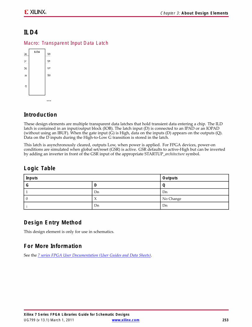
Chapter 3: About Design Elements
ILD4Macro: Transparent Input Data Latch
IntroductionThese design elements are multiple transparent data latches that hold transient data entering a chip. The ILDlatch is contained in an input/output block (IOB). The latch input (D) is connected to an IPAD or an IOPAD(without using an IBUF). When the gate input (G) is High, data on the inputs (D) appears on the outputs (Q).Data on the D inputs during the High-to-Low G transition is stored in the latch.
This latch is asynchronously cleared, outputs Low, when power is applied. For FPGA devices, power-onconditions are simulated when global set/reset (GSR) is active. GSR defaults to active-High but can be invertedby adding an inverter in front of the GSR input of the appropriate STARTUP_architecture symbol.
Logic TableInputs Outputs
G D Q1 Dn Dn
0 X No Change
↓ Dn Dn
Design Entry MethodThis design element is only for use in schematics.
For More InformationSee the 7 series FPGA User Documentation (User Guides and Data Sheets).
Xilinx 7 Series FPGA Libraries Guide for Schematic DesignsUG799 (v 13.1) March 1, 2011 www.xilinx.com 253

Chapter 3: About Design Elements
ILD8Macro: Transparent Input Data Latch
IntroductionThese design elements are multiple transparent data latches that hold transient data entering a chip. The ILDlatch is contained in an input/output block (IOB). The latch input (D) is connected to an IPAD or an IOPAD(without using an IBUF). When the gate input (G) is High, data on the inputs (D) appears on the outputs (Q).Data on the D inputs during the High-to-Low G transition is stored in the latch.
This latch is asynchronously cleared, outputs Low, when power is applied. For FPGA devices, power-onconditions are simulated when global set/reset (GSR) is active. GSR defaults to active-High but can be invertedby adding an inverter in front of the GSR input of the appropriate STARTUP_architecture symbol.
Logic TableInputs Outputs
G D Q1 Dn Dn
0 X No Change
↓ Dn Dn
Design Entry MethodThis design element is only for use in schematics.
For More InformationSee the 7 series FPGA User Documentation (User Guides and Data Sheets).
Xilinx 7 Series FPGA Libraries Guide for Schematic Designs254 www.xilinx.com UG799 (v 13.1) March 1, 2011

Chapter 3: About Design Elements
ILDIMacro: Transparent Input Data Latch (Asynchronous Preset)
IntroductionThis design element is a transparent data latch that holds transient data entering a chip. When the gate input(G) is High, data on the input (D) appears on the output (Q). Data on the D input during the High-to-Low Gtransition is stored in the latch.
The ILDI is the input flip-flop master latch. It is possible to access two different outputs from the inputflip-flop: one that responds to the level of the clock signal and another that responds to an edge of the clocksignal. When using both outputs from the same input flip-flop, a transparent High latch (ILDI) corresponds toa falling edge-triggered flip-flop (IFDI_1). Similarly, a transparent Low latch (ILDI_1) corresponds to a risingedge-triggered flip-flop (IFDI).
The latch is asynchronously preset, output High, when power is applied.
For FPGA devices, power-on conditions are simulated when global set/reset (GSR) is active. GSR defaultsto active-High but can be inverted by adding an inverter in front of the GSR input of the appropriateSTARTUP_architecture symbol.
Logic TableInputs Outputs
G D Q1 D D
0 X No Change
↓ D D
Design Entry MethodThis design element is only for use in schematics.
For More InformationSee the 7 series FPGA User Documentation (User Guides and Data Sheets).
Xilinx 7 Series FPGA Libraries Guide for Schematic DesignsUG799 (v 13.1) March 1, 2011 www.xilinx.com 255
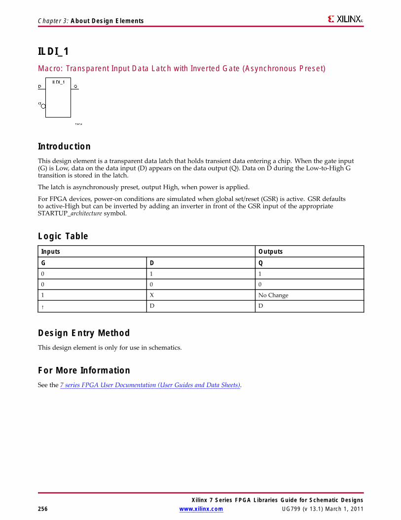
Chapter 3: About Design Elements
ILDI_1Macro: Transparent Input Data Latch with Inverted Gate (Asynchronous Preset)
IntroductionThis design element is a transparent data latch that holds transient data entering a chip. When the gate input(G) is Low, data on the data input (D) appears on the data output (Q). Data on D during the Low-to-High Gtransition is stored in the latch.
The latch is asynchronously preset, output High, when power is applied.
For FPGA devices, power-on conditions are simulated when global set/reset (GSR) is active. GSR defaultsto active-High but can be inverted by adding an inverter in front of the GSR input of the appropriateSTARTUP_architecture symbol.
Logic TableInputs Outputs
G D Q0 1 1
0 0 0
1 X No Change
↑ D D
Design Entry MethodThis design element is only for use in schematics.
For More InformationSee the 7 series FPGA User Documentation (User Guides and Data Sheets).
Xilinx 7 Series FPGA Libraries Guide for Schematic Designs256 www.xilinx.com UG799 (v 13.1) March 1, 2011

Chapter 3: About Design Elements
ILDXIMacro: Transparent Input Data Latch (Asynchronous Preset)
IntroductionThis design element is a transparent data latch that holds transient data entering a chip. When the gate input (G)is High, data on the input (D) appears on the output (Q). Data on the (D) input during the High-to-Low (G)transition is stored in the latch.
The ILDXI is the input flip-flop master latch. Two outputs can be accessed from the input flip-flop: one thatresponds to the level of the clock signal and another that responds to an edge of the clock signal. Whenusing both outputs from the same input flip-flop, a transparent High latch (ILDXI) corresponds to a fallingedge-triggered flip-flop (IFDXI_1). Similarly, a transparent Low latch (ILDXI_1) corresponds to a risingedge-triggered flip-flop (IFDXI).
The latch is asynchronously preset, output High, when power is applied.
For FPGA devices, power-on conditions are simulated when global set/reset (GSR) is active. GSR defaultsto active-High but can be inverted by adding an inverter in front of the GSR input of the appropriateSTARTUP_architecture symbol.
Logic TableInputs Outputs
GE G D Q0 X X No Change
1 0 X No Change
1 1 D D
1 ↓ D D
Design Entry MethodThis design element is only for use in schematics.
For More InformationSee the 7 series FPGA User Documentation (User Guides and Data Sheets).
Xilinx 7 Series FPGA Libraries Guide for Schematic DesignsUG799 (v 13.1) March 1, 2011 www.xilinx.com 257

Chapter 3: About Design Elements
ILDXI_1Macro: Transparent Input Data Latch with Inverted Gate (Asynchronous Preset)
IntroductionThis design element is a transparent data latch that holds transient data entering a chip.
The latch is asynchronously preset, output High, when power is applied.
For FPGA devices, power-on conditions are simulated when global set/reset (GSR) is active. GSR defaultsto active-High but can be inverted by adding an inverter in front of the GSR input of the appropriateSTARTUP_architecture symbol.
Logic TableInputs Outputs
GE G D Q0 X X No Change
1 1 X No Change
1 0 D D
1 ↑ D D
Design Entry MethodThis design element is only for use in schematics.
For More InformationSee the 7 series FPGA User Documentation (User Guides and Data Sheets).
Xilinx 7 Series FPGA Libraries Guide for Schematic Designs258 www.xilinx.com UG799 (v 13.1) March 1, 2011

Chapter 3: About Design Elements
INVPrimitive: Inverter
IntroductionThis design element is a single inverter that identifies signal inversions in a schematic.
Design Entry MethodThis design element is only for use in schematics.
For More InformationSee the 7 series FPGA User Documentation (User Guides and Data Sheets).
Xilinx 7 Series FPGA Libraries Guide for Schematic DesignsUG799 (v 13.1) March 1, 2011 www.xilinx.com 259

Chapter 3: About Design Elements
INV16Macro: 16 Inverters
IntroductionThis design element is a multiple inverter that identifies signal inversions in a schematic.
Design Entry MethodThis design element is only for use in schematics.
For More InformationSee the 7 series FPGA User Documentation (User Guides and Data Sheets).
Xilinx 7 Series FPGA Libraries Guide for Schematic Designs260 www.xilinx.com UG799 (v 13.1) March 1, 2011

Chapter 3: About Design Elements
INV4Macro: Four Inverters
IntroductionThis design element is a multiple inverter that identifies signal inversions in a schematic.
Design Entry MethodThis design element is only for use in schematics.
For More InformationSee the 7 series FPGA User Documentation (User Guides and Data Sheets).
Xilinx 7 Series FPGA Libraries Guide for Schematic DesignsUG799 (v 13.1) March 1, 2011 www.xilinx.com 261

Chapter 3: About Design Elements
INV8Macro: Eight Inverters
IntroductionThis design element is a multiple inverter that identifies signal inversions in a schematic.
Design Entry MethodThis design element is only for use in schematics.
For More InformationSee the 7 series FPGA User Documentation (User Guides and Data Sheets).
Xilinx 7 Series FPGA Libraries Guide for Schematic Designs262 www.xilinx.com UG799 (v 13.1) March 1, 2011

Chapter 3: About Design Elements
IOBUFPrimitive: Bi-Directional Buffer
IntroductionThe design element is a bidirectional single-ended I/O Buffer used to connect internal logic to an externalbidirectional pin.
Logic TableInputs Bidirectional Outputs
T I IO O1 X Z IO
0 1 1 1
0 0 0 0
Port DescriptionsPort Direction Width FunctionO Output 1 Buffer output
IO Inout 1 Buffer inout
I Input 1 Buffer input
T Input 1 3-State enable input
Design Entry MethodThis design element can be used in schematics.
Available AttributesAttribute Type Allowed Values Default DescriptionDRIVE Integer 2, 4, 6, 8, 12, 16, 24 12 Selects output drive strength (mA)
for the SelectIO™ buffers that usethe LVTTL, LVCMOS12, LVCMOS15,LVCMOS18, LVCMOS25, or LVCMOS33interface I/O standard.
IOSTANDARD String See Data Sheet "DEFAULT" Assigns an I/O standard to the element.
SLEW String "SLOW", "FAST","QUIETIO"
"SLOW" Sets the output rise and fall time. See theData Sheet for recommendations of thebest setting for this attribute.
For More Information
Xilinx 7 Series FPGA Libraries Guide for Schematic DesignsUG799 (v 13.1) March 1, 2011 www.xilinx.com 263

Chapter 3: About Design Elements
IOBUFDSPrimitive: 3-State Differential Signaling I/O Buffer with Active Low Output Enable
IntroductionThe design element is a bidirectional buffer that supports low-voltage, differential signaling. For the IOBUFDS, adesign level interface signal is represented as two distinct ports (IO and IOB), one deemed the "master" andthe other the "slave." The master and the slave are opposite phases of the same logical signal (for example,MYNET_P and MYNET_N). Optionally, a programmable differential termination feature is available to helpimprove signal integrity and reduce external components. Also available is a programmable delay is to assist inthe capturing of incoming data to the device.
Logic TableInputs Bidirectional Outputs
I T IO IOB OX 1 Z Z No Change
0 0 0 1 0
I 0 1 0 1
Port DescriptionsPort Direction Width FunctionO Output 1 Buffer output
IO Inout 1 Diff_p inout
IOB Inout 1 Diff_n inout
I Input 1 Buffer input
T Input 1 3-state enable input
Design Entry MethodThis design element can be used in schematics.
Available AttributesAttribute Type Allowed Values Default DescriptionIOSTANDARD String See Data Sheet "DEFAULT" Assigns an I/O standard to the element.
For More Information
Xilinx 7 Series FPGA Libraries Guide for Schematic Designs264 www.xilinx.com UG799 (v 13.1) March 1, 2011

Chapter 3: About Design Elements
ISERDESE2Primitive: Input SERial/DESerializer with bitslip
IntroductionThe ISERDESE2 in 7 series FPGAs is a dedicated serial-to-parallel converter with specific clocking and logicfeatures designed to facilitate the implementation of high-speed sourcesynchronous applications. TheISERDESE2 avoids the additional timing complexities encountered when designing deserializers in the FPGAfabric. ISERDESE2 features include: - Dedicated Deserializer/Serial-to-Parallel Converter The ISERDESE1deserializer enables high-speed data transfer without requiring the FPGA fabric to match the input datafrequency. This converter supports both single data rate (SDR) and double data rate (DDR) modes. In SDRmode, the serial-to-parallel converter creates a 2-, 3-, 4-, 5-, 6-, 7-, or 8-bit wide parallel word. In DDR mode,the serial-to-parallel converter creates a 4-, 6-, 8-, 10-, or 14-bit-wide parallel word. - Bitslip Submodule TheBitslip submodule allows designers to reorder the sequence of the parallel data stream going into the FPGAfabric. This can be used for training source-synchronous interfaces that include a training pattern. - DedicatedSupport for Strobe-based Memory Interfaces ISERDESE2 contains dedicated circuitry (including the OCLK inputpin) to handle the strobe-to-FPGA clock domain crossover entirely within the ISERDESE2 block. This allowsfor higher performance and a simplified implementation. - Dedicated Support for Networking Interfaces -Dedicated Support for Memory Interfaces
Port DescriptionsPort Type Width FunctionBITSLIP Input 1 The BITSLIP pin performs a Bitslip operation synchronous to CLKDIV
when asserted (active High). Subsequently, the data seen on the Q1 toQ8 output ports will shift, as in a barrel-shifter operation, one positionevery time Bitslip is invoked (DDR operation is different from SDR).
Xilinx 7 Series FPGA Libraries Guide for Schematic DesignsUG799 (v 13.1) March 1, 2011 www.xilinx.com 265

Chapter 3: About Design Elements
Port Type Width FunctionCE1, CE2 Input 1 Each ISERDESE2 block contains an input clock enable module. When
NUM_CE = 1, the CE2 input is not used, and the CE1 input is anactive high clock enable connected directly to the input registers in theISERDESE2. WhenNUM_CE = 2, the CE1 and CE2 inputs are both used,with CE1 enabling the ISERDESE2 for half of a CLKDIV cycle, and CE2enabling the ISERDESE2 for the other half. The clock enable modulefunctions as a 2:1 serial-to-parallel converter, clocked by CLKDIV. Theclock enable module is needed specifically for bidirectional memoryinterfaces when ISERDESE1 is configured for 1:4 deserialization in DDRmode. When the attribute NUM_CE = 2, the clock enable module isenabled and both CE1 and CE2 ports are available. When NUM_CE = 1,only CE1 is available and functions as a regular clock enable.
CLK Input 1 The high-speed clock input (CLK) is used to clock in the input serialdata stream.
CLKB Input 1 The high-speed secondary clock input (CLKB) is used to clock in theinput serial data stream. In any mode other than MEMORY_QDR,connect CLKB to an inverted version of CLK. In MEMORY_QDR modeCLKB should be connected to a unique, phase shifted clock.
CLKDIV Input 1 The divided clock input (CLKDIV) is typically a divided version of CLK(depending on the width of the implemented deserialization). It drivesthe output of the serial-to-parallel converter, the Bitslip submodule,and the CE module.
CLKDIVP Input 1 Divided clock to be used for parallelized data.
D Input 1 The serial input data port (D) is the serial (high-speed) data input portof the ISERDESE2. This port works in conjunction only with the 7 seriesFPGA IOB resource.
DDLY Input 1 The serial input data port (DDLY) is the serial (high-speed) data inputport of the ISERDESE2. This port works in conjunction only with the 7series FPGA IDELAYE2 resource.
DYNCLKDIVSEL Input 1 Dynamically select CLKDIV inversion.
DYNCLKSEL Input 1 Dynamically select CLK and CLKB inversion. Dynamically selectOCLK inversion.
O Output 1 The combinatorial output port (O) is an unregistered output of theISERDESE2 module. This output can come directly from the data input(D), or from the data input (DDLY) via the IDELAYE2.
OCLK Input 1 The OCLK clock input synchronizes data transfer in strobe-basedmemory interfaces. The OCLK clock is only used whenINTERFACE_TYPE is set to MEMORY.
OCLKB Input 1 The OCLK clock input synchronizes data transfer in strobe-basedmemory interfaces. The OCLKB clock is only used whenINTERFACE_TYPE is set to MEMORY.
OFB Input 1 The serial input data port (OFB) is the serial (high-speed) data inputport of the ISERDESE2. This port works in conjunction only with the 7series FPGA OSERDESE2 port OFB.
Q1 - Q8 Output 1 The output ports Q1 to Q8 are the registered outputs of the ISERDESE2module. One ISERDESE2 block can support up to eight bits (i.e., a1:8 deserialization). Bit widths greater than eight (up to 14) can besupported.
Xilinx 7 Series FPGA Libraries Guide for Schematic Designs266 www.xilinx.com UG799 (v 13.1) March 1, 2011

Chapter 3: About Design Elements
Port Type Width FunctionRST Input 1 The reset input causes the outputs of all data flip-flops in the CLK
and CLKDIV domains to be driven low asynchronously. ISERDESE2circuits running in the CLK domain where timing is critical use aninternal, dedicated circuit to retime the RST input to produce a resetsignal synchronous to the CLK domain. Similarly, there is a dedicatedcircuit to retime the RST input to produce a reset signal synchronousto the CLKDIV domain. Because the ISERDESE2 is driven into resetasynchronously but comes out of reset synchronously it must betreated as a synchronous reset to the CLKDIV time domain and havea minimum pulse of one CLKDIV cycle. When building an interfaceconsisting of multiple ISERDESE2 ports, all ISERDESE2 ports in theinterface must be synchronized. The internal retiming of the RST inputis designed so that all ISERDESE2 blocks that receive the same resetpulse come out of reset synchronized with one another.
SHIFTIN1 /SHIFTIN2
Input 1 If ISERDES_MODE="SLAVE", connect to the master ISERDESE2SHIFTOUT1/2 outputs. Otherwise, these pins must be grounded.
SHIFTOUT1 /SHIFTOUT2
Output 1 If ISERDES_MODE="MASTER" and two ISERDESE2 are to be cascaded,connect to the slave ISERDESE2 SHIFTIN1/2 inputs.
Design Entry MethodThis design element can be used in schematics.
Available AttributesAttribute Type Allowed Values Default DescriptionDATA_RATE STRING DDR, SDR DDR The DATA_RATE attribute defines
whether the incoming data stream isprocessed as single data rate (SDR) ordouble data rate (DDR).
DATA_WIDTH DECIMAL 4, 2, 3, 5, 6, 7, 8, 10, 14 4 Defines the width of theserial-to-parallel converter. The legalvalue depends on the DATA_RATEattribute (SDR or DDR). Integer: 2, 3,4, 5, 6, 7, 8, or 10. If DATA_RATE =DDR, value is limited to 4, 6, 8, or 10. IfDATA_RATE = SDR, value is limited to2, 3, 4, 5, 6, 7, or 8.
DYN_CLK_INV_EN
STRING FALSE, TRUE FALSE Enables DYNCLKINVSEL inversionwhen "TRUE" and disables HDLinversions on CLK and CLKB pins.
DYN_CLKDIV_INV_EN
STRING FALSE, TRUE FALSE Enables DYNCLKDIVINVSELinversion when "TRUE" and disablesHDL inversions on CLKDIV pin
INIT_Q1 BINARY 1’b0 to 1’b1 1’b0 Initial (post-configuration) value on Q1output.
INIT_Q2 BINARY 1’b0 to 1’b1 1’b0 Initial (post-configuration) value on Q2output.
INIT_Q3 BINARY 1’b0 to 1’b1 1’b0 Initial (post-configuration) value on Q3output.
INIT_Q4 BINARY 1’b0 to 1’b1 1’b0 Initial (post-configuration) value on Q4output.
Xilinx 7 Series FPGA Libraries Guide for Schematic DesignsUG799 (v 13.1) March 1, 2011 www.xilinx.com 267

Chapter 3: About Design Elements
Attribute Type Allowed Values Default DescriptionINTERFACE_TYPE
STRING MEMORY,MEMORY_DDR3,MEMORY_QDR,NETWORKING,OVERSAMPLE
MEMORY Chooses memory, networking orover-sample interface type use models.
IOBDELAY STRING NONE, BOTH, IBUF,IFD
NONE Defines input sources for ISERDESmodule.
NUM_CE DECIMAL 2, 1 2 Defines the number of clock enables.
OFB_USED STRING FALSE, TRUE FALSE Enables the path from the OLOGIC,OSERDESOFB pin to the ISERDESOFBpin. Disables the use of the D input pin.
SERDES_MODE STRING MASTER, SLAVE MASTER Defines whether the ISERDESE2module is a master or slave when usingwidth expansion.
SRVAL_Q1 BINARY 1’b0 to 1’b1 1’b0 Set/reset on Q1 output.
SRVAL_Q2 BINARY 1’b0 to 1’b1 1’b0 Set/reset on Q2 output.
SRVAL_Q3 BINARY 1’b0 to 1’b1 1’b0 Set/reset on Q3 output.
SRVAL_Q4 BINARY 1’b0 to 1’b1 1’b0 Set/reset on Q4 output.
For More Information• See the 7 series FPGA SelectIO Resources User Guide.
• See the 7 series FPGA Data Sheet DC and Switching Characteristics.
Xilinx 7 Series FPGA Libraries Guide for Schematic Designs268 www.xilinx.com UG799 (v 13.1) March 1, 2011

Chapter 3: About Design Elements
KEEPERPrimitive: KEEPER Symbol
IntroductionThe design element is a weak keeper element that retains the value of the net connected to its bidirectional O pin.For example, if a logic 1 is being driven onto the net, KEEPER drives a weak/resistive 1 onto the net. If the netdriver is then 3-stated, KEEPER continues to drive a weak/resistive 1 onto the net.
Port DescriptionsName Direction Width FunctionO Output 1-Bit Keeper output
Design Entry MethodThis design element can be used in schematics or instantiated in HDL code. Instantiation templates for VHDLand Verilog are available below.
This element can be connected to a net in the following locations on a top-level schematic file:
• A net connected to an input IO Marker
• A net connected to both an output IO Marker and 3-statable IO element, such as an OBUFT.
For More Information
Xilinx 7 Series FPGA Libraries Guide for Schematic DesignsUG799 (v 13.1) March 1, 2011 www.xilinx.com 269

Chapter 3: About Design Elements
KEY_CLEARPrimitive: Virtex-5 Configuration Encryption Key Erase
IntroductionThis design element allows you to erase the configuration encryption circuit key register from internal logic.
Port DescriptionsPort Direction Width FunctionKEYCLEARB Input 1 Active low input, clears the
configuration encryptionkey
Design Entry MethodThis design element can be used in schematics.
For More InformationSee the 7 series FPGA User Documentation (User Guides and Data Sheets).
Xilinx 7 Series FPGA Libraries Guide for Schematic Designs270 www.xilinx.com UG799 (v 13.1) March 1, 2011

Chapter 3: About Design Elements
LDPrimitive: Transparent Data Latch
IntroductionLD is a transparent data latch. The data output (Q) of the latch reflects the data (D) input while the gate enable(G) input is High. The data on the (D) input during the High-to-Low gate transition is stored in the latch. Thedata on the (Q) output remains unchanged as long as (G) remains Low.
This latch is asynchronously cleared, outputs Low, when power is applied. For FPGA devices, power-onconditions are simulated when global set/reset (GSR) is active. GSR defaults to active-High but can be invertedby adding an inverter in front of the GSR input of the appropriate STARTUP_architecture symbol.
Logic TableInputs Outputs
G D Q1 D D
0 X No Change
↓ D D
Design Entry MethodThis design element is only for use in schematics.
Available Attributes
Attribute TypeAllowedValues Default Description
INIT Binary 0, 1 0 Sets the initial value of Q output after configuration
For More InformationSee the 7 series FPGA User Documentation (User Guides and Data Sheets).
Xilinx 7 Series FPGA Libraries Guide for Schematic DesignsUG799 (v 13.1) March 1, 2011 www.xilinx.com 271

Chapter 3: About Design Elements
LD_1Primitive: Transparent Data Latch with Inverted Gate
IntroductionThis design element is a transparent data latch with an inverted gate. The data output (Q) of the latch reflects thedata (D) input while the gate enable (G) input is Low. The data on the (D) input during the Low-to-High gatetransition is stored in the latch. The data on the (Q) output remains unchanged as long as (G) remains High.
This latch is asynchronously cleared, outputs Low, when power is applied. For FPGA devices, power-onconditions are simulated when global set/reset (GSR) is active. GSR defaults to active-High but can be invertedby adding an inverter in front of the GSR input of the appropriate STARTUP_architecture symbol.
Logic TableInputs Outputs
G D Q0 D D
1 X No Change
↑ D D
Design Entry MethodThis design element is only for use in schematics.
Available Attributes
Attribute TypeAllowedValues Default Description
INIT Binary 0, 1 0 Sets the initial value of Q output after configuration.
For More InformationSee the 7 series FPGA User Documentation (User Guides and Data Sheets).
Xilinx 7 Series FPGA Libraries Guide for Schematic Designs272 www.xilinx.com UG799 (v 13.1) March 1, 2011

Chapter 3: About Design Elements
LD16Macro: Multiple Transparent Data Latch
IntroductionThis design element has 16 transparent data latches with a common gate enable (G). The data output (Q) of thelatch reflects the data (D) input while the gate enable (G) input is High. The data on the (D) input during theHigh-to-Low gate transition is stored in the latch. The data on the (Q) output remains unchanged as long as(G) remains Low.
This latch is asynchronously cleared, outputs Low, when power is applied. For FPGA devices, power-onconditions are simulated when global set/reset (GSR) is active. GSR defaults to active-High but can be invertedby adding an inverter in front of the GSR input of the appropriate STARTUP_architecture symbol.
Logic TableInputs Outputs
G D Q1 Dn Dn
0 X No Change
↓ Dn Dn
Design Entry MethodThis design element is only for use in schematics.
Available Attributes
Attribute TypeAllowedValues Default Description
INIT Binary Any 16-Bit Value All zeros Sets the initial value of Q output afterconfiguration
For More InformationSee the 7 series FPGA User Documentation (User Guides and Data Sheets).
Xilinx 7 Series FPGA Libraries Guide for Schematic DesignsUG799 (v 13.1) March 1, 2011 www.xilinx.com 273

Chapter 3: About Design Elements
LD16CEMacro: Transparent Data Latch with Asynchronous Clear and Gate Enable
IntroductionThis design element has 16 transparent data latches with asynchronous clear and gate enable. When theasynchronous clear input (CLR) is High, it overrides the other inputs and resets the data (Q) outputs Low. (Q)reflects the data (D) inputs while the gate (G) and gate enable (GE) are High, and (CLR) is Low. If (GE) is Low,data on (D) cannot be latched. The data on the (D) input during the High-to-Low gate transition is stored in thelatch. The data on the (Q) output remains unchanged as long as (G) or (GE) remains Low.
This latch is asynchronously cleared, outputs Low, when power is applied. For FPGA devices, power-onconditions are simulated when global set/reset (GSR) is active. GSR defaults to active-High but can be invertedby adding an inverter in front of the GSR input of the appropriate STARTUP_architecture symbol.
Logic TableInputs Outputs
CLR GE G Dn Qn1 X X X 0
0 0 X X No Change
0 1 1 Dn Dn
0 1 0 X No Change
0 1 ↓ Dn Dn
Design Entry MethodThis design element is only for use in schematics.
Available Attributes
Attribute TypeAllowedValues Default Description
INIT Binary Any 16-BitValue
All zeros Sets the initial value of Q output after configuration
For More InformationSee the 7 series FPGA User Documentation (User Guides and Data Sheets).
Xilinx 7 Series FPGA Libraries Guide for Schematic Designs274 www.xilinx.com UG799 (v 13.1) March 1, 2011

Chapter 3: About Design Elements
LD4Macro: Multiple Transparent Data Latch
IntroductionThis design element has four transparent data latches with a common gate enable (G). The data output (Q) of thelatch reflects the data (D) input while the gate enable (G) input is High. The data on the (D) input during theHigh-to-Low gate transition is stored in the latch. The data on the (Q) output remains unchanged as long as(G) remains Low.
This latch is asynchronously cleared, outputs Low, when power is applied. For FPGA devices, power-onconditions are simulated when global set/reset (GSR) is active. GSR defaults to active-High but can be invertedby adding an inverter in front of the GSR input of the appropriate STARTUP_architecture symbol.
Logic TableInputs Outputs
G D Q1 Dn Dn
0 X No Change
↓ Dn Dn
Design Entry MethodThis design element is only for use in schematics.
Available Attributes
Attribute TypeAllowedValues Default Description
INIT Binary Any 4-Bit Value All zeros Sets the initial value of Q output after configuration
For More InformationSee the 7 series FPGA User Documentation (User Guides and Data Sheets).
Xilinx 7 Series FPGA Libraries Guide for Schematic DesignsUG799 (v 13.1) March 1, 2011 www.xilinx.com 275

Chapter 3: About Design Elements
LD4CEMacro: Transparent Data Latch with Asynchronous Clear and Gate Enable
IntroductionThis design element has 4 transparent data latches with asynchronous clear and gate enable. When theasynchronous clear input (CLR) is High, it overrides the other inputs and resets the data (Q) outputs Low. (Q)reflects the data (D) inputs while the gate (G) and gate enable (GE) are High, and (CLR) is Low. If (GE) is Low,data on (D) cannot be latched. The data on the (D) input during the High-to-Low gate transition is stored in thelatch. The data on the (Q) output remains unchanged as long as (G) or (GE) remains Low.
This latch is asynchronously cleared, outputs Low, when power is applied. For FPGA devices, power-onconditions are simulated when global set/reset (GSR) is active. GSR defaults to active-High but can be invertedby adding an inverter in front of the GSR input of the appropriate STARTUP_architecture symbol.
Logic TableInputs Outputs
CLR GE G Dn Qn1 X X X 0
0 0 X X No Change
0 1 1 Dn Dn
0 1 0 X No Change
0 1 ↓ Dn Dn
Design Entry MethodThis design element is only for use in schematics.
Available Attributes
Attribute TypeAllowedValues Default Description
INIT Binary Any 4-BitValue
All zeros Sets the initial value of Q output afterconfiguration
For More InformationSee the 7 series FPGA User Documentation (User Guides and Data Sheets).
Xilinx 7 Series FPGA Libraries Guide for Schematic Designs276 www.xilinx.com UG799 (v 13.1) March 1, 2011
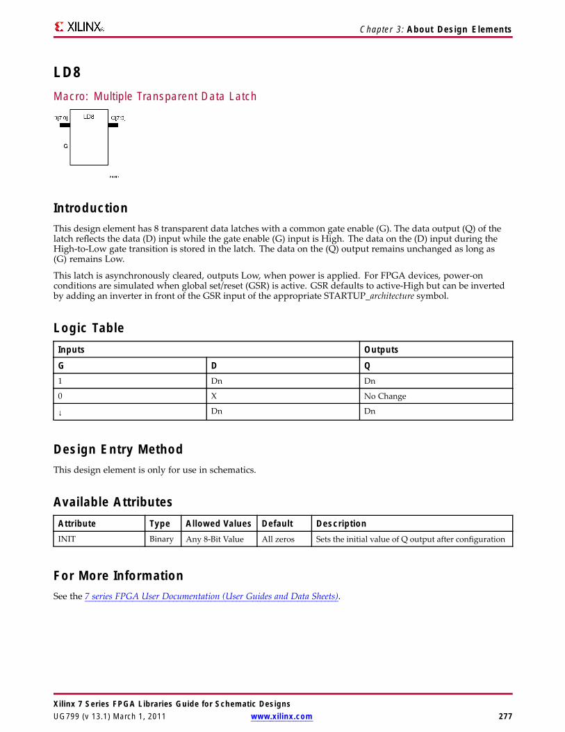
Chapter 3: About Design Elements
LD8Macro: Multiple Transparent Data Latch
IntroductionThis design element has 8 transparent data latches with a common gate enable (G). The data output (Q) of thelatch reflects the data (D) input while the gate enable (G) input is High. The data on the (D) input during theHigh-to-Low gate transition is stored in the latch. The data on the (Q) output remains unchanged as long as(G) remains Low.
This latch is asynchronously cleared, outputs Low, when power is applied. For FPGA devices, power-onconditions are simulated when global set/reset (GSR) is active. GSR defaults to active-High but can be invertedby adding an inverter in front of the GSR input of the appropriate STARTUP_architecture symbol.
Logic TableInputs Outputs
G D Q1 Dn Dn
0 X No Change
↓ Dn Dn
Design Entry MethodThis design element is only for use in schematics.
Available AttributesAttribute Type Allowed Values Default DescriptionINIT Binary Any 8-Bit Value All zeros Sets the initial value of Q output after configuration
For More InformationSee the 7 series FPGA User Documentation (User Guides and Data Sheets).
Xilinx 7 Series FPGA Libraries Guide for Schematic DesignsUG799 (v 13.1) March 1, 2011 www.xilinx.com 277
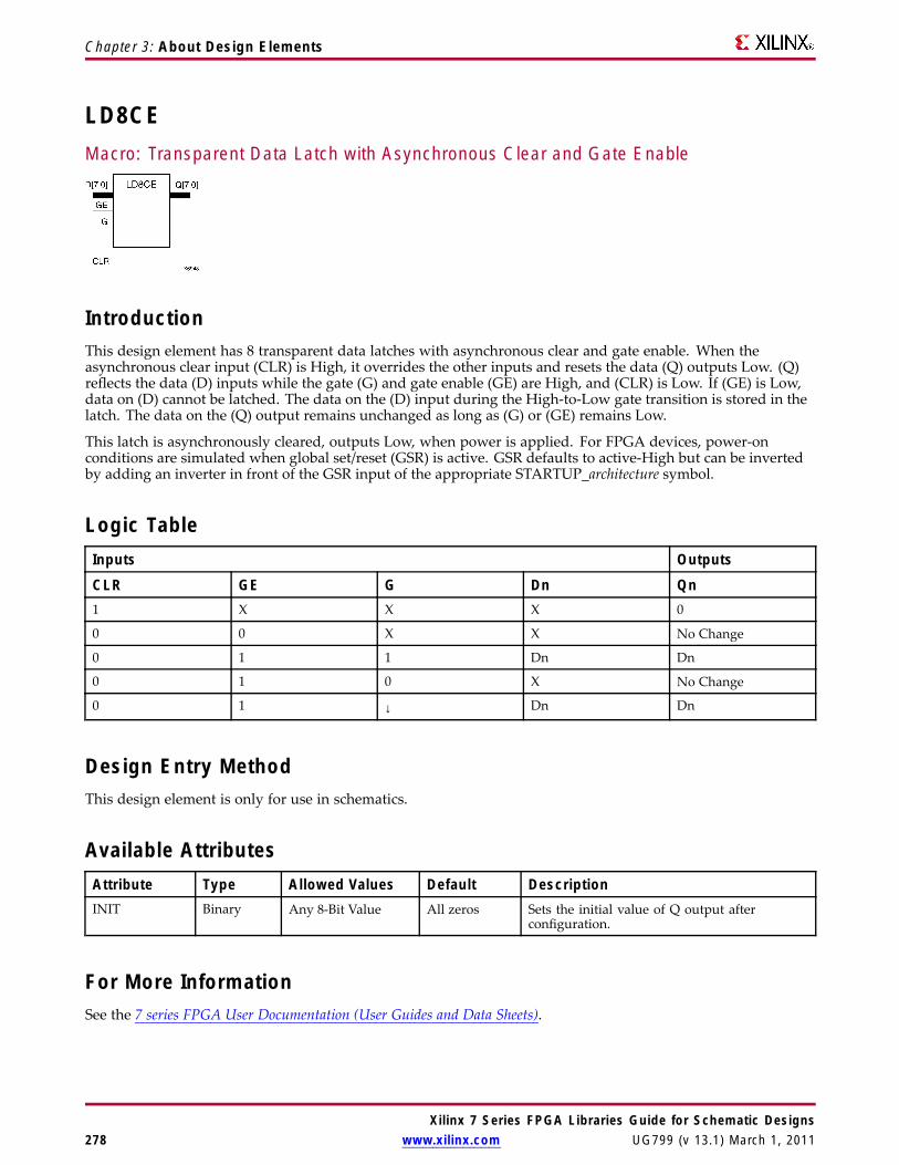
Chapter 3: About Design Elements
LD8CEMacro: Transparent Data Latch with Asynchronous Clear and Gate Enable
IntroductionThis design element has 8 transparent data latches with asynchronous clear and gate enable. When theasynchronous clear input (CLR) is High, it overrides the other inputs and resets the data (Q) outputs Low. (Q)reflects the data (D) inputs while the gate (G) and gate enable (GE) are High, and (CLR) is Low. If (GE) is Low,data on (D) cannot be latched. The data on the (D) input during the High-to-Low gate transition is stored in thelatch. The data on the (Q) output remains unchanged as long as (G) or (GE) remains Low.
This latch is asynchronously cleared, outputs Low, when power is applied. For FPGA devices, power-onconditions are simulated when global set/reset (GSR) is active. GSR defaults to active-High but can be invertedby adding an inverter in front of the GSR input of the appropriate STARTUP_architecture symbol.
Logic TableInputs Outputs
CLR GE G Dn Qn1 X X X 0
0 0 X X No Change
0 1 1 Dn Dn
0 1 0 X No Change
0 1 ↓ Dn Dn
Design Entry MethodThis design element is only for use in schematics.
Available AttributesAttribute Type Allowed Values Default DescriptionINIT Binary Any 8-Bit Value All zeros Sets the initial value of Q output after
configuration.
For More InformationSee the 7 series FPGA User Documentation (User Guides and Data Sheets).
Xilinx 7 Series FPGA Libraries Guide for Schematic Designs278 www.xilinx.com UG799 (v 13.1) March 1, 2011

Chapter 3: About Design Elements
LDCPrimitive: Transparent Data Latch with Asynchronous Clear
IntroductionThis design element is a transparent data latch with asynchronous clear. When the asynchronous clear input(CLR) is High, it overrides the other inputs and resets the data (Q) output Low. (Q) reflects the data (D) inputwhile the gate enable (G) input is High and (CLR) is Low. The data on the (D) input during the High-to-Low gatetransition is stored in the latch. The data on the (Q) output remains unchanged as long as (G) remains low.
This latch is asynchronously cleared, outputs Low, when power is applied. For FPGA devices, power-onconditions are simulated when global set/reset (GSR) is active. GSR defaults to active-High but can be invertedby adding an inverter in front of the GSR input of the appropriate STARTUP_architecture symbol.
Logic TableInputs Outputs
CLR G D Q1 X X 0
0 1 D D
0 0 X No Change
0 ↓ D D
Design Entry MethodThis design element is only for use in schematics.
Available AttributesAttribute Type Allowed Values Default DescriptionINIT Binary 0, 1 0 Sets the initial value of Q output after
configuration.
For More InformationSee the 7 series FPGA User Documentation (User Guides and Data Sheets).
Xilinx 7 Series FPGA Libraries Guide for Schematic DesignsUG799 (v 13.1) March 1, 2011 www.xilinx.com 279

Chapter 3: About Design Elements
LDC_1Primitive: Transparent Data Latch with Asynchronous Clear and Inverted Gate
IntroductionThis design element is a transparent data latch with asynchronous clear and inverted gate. When theasynchronous clear input (CLR) is High, it overrides the other inputs (D and G) and resets the data (Q) outputLow. (Q) reflects the data (D) input while the gate enable (G) input and CLR are Low. The data on the (D) inputduring the Low-to-High gate transition is stored in the latch. The data on the (Q) output remains unchanged aslong as (G) remains High.
This latch is asynchronously cleared, outputs Low, when power is applied. For FPGA devices, power-onconditions are simulated when global set/reset (GSR) is active. GSR defaults to active-High but can be invertedby adding an inverter in front of the GSR input of the appropriate STARTUP_architecture symbol.
Logic TableInputs Outputs
CLR G D Q1 X X 0
0 0 D D
0 1 X No Change
0 ↑ D D
Design Entry MethodThis design element is only for use in schematics.
Available AttributesAttribute Type Allowed Values Default DescriptionINIT Binary 0, 1 0 Sets the initial value of Q output after configuration.
For More InformationSee the 7 series FPGA User Documentation (User Guides and Data Sheets).
Xilinx 7 Series FPGA Libraries Guide for Schematic Designs280 www.xilinx.com UG799 (v 13.1) March 1, 2011
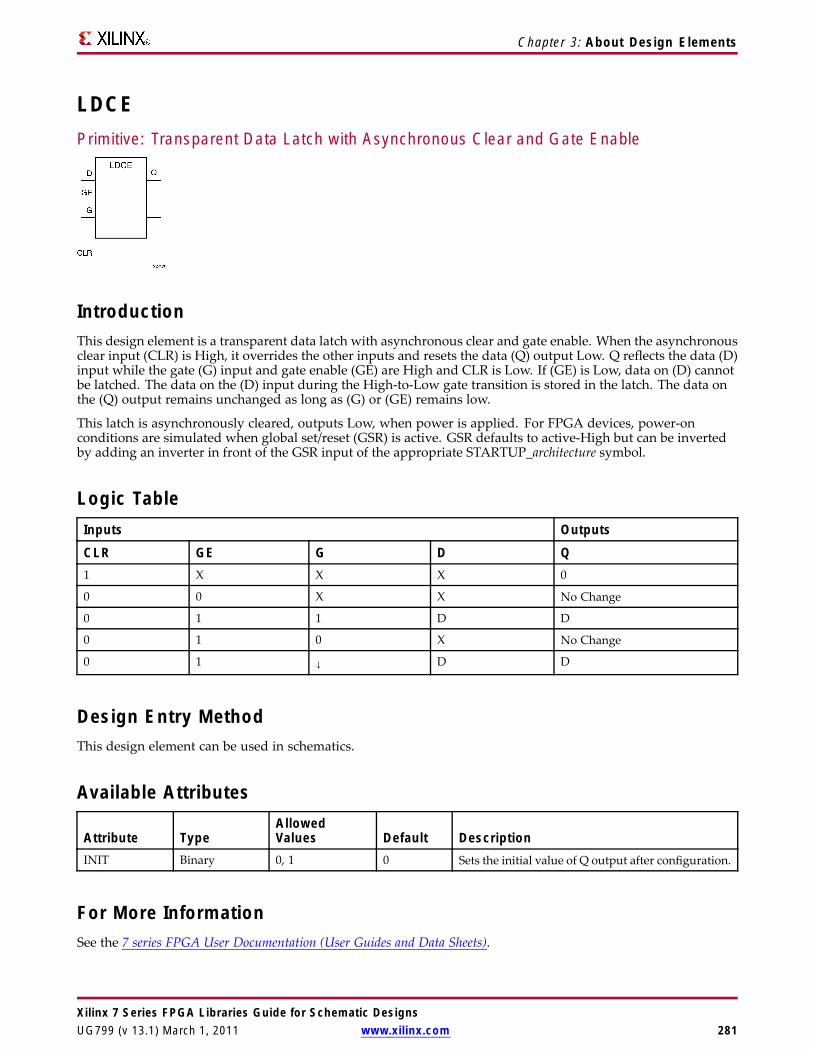
Chapter 3: About Design Elements
LDCEPrimitive: Transparent Data Latch with Asynchronous Clear and Gate Enable
IntroductionThis design element is a transparent data latch with asynchronous clear and gate enable. When the asynchronousclear input (CLR) is High, it overrides the other inputs and resets the data (Q) output Low. Q reflects the data (D)input while the gate (G) input and gate enable (GE) are High and CLR is Low. If (GE) is Low, data on (D) cannotbe latched. The data on the (D) input during the High-to-Low gate transition is stored in the latch. The data onthe (Q) output remains unchanged as long as (G) or (GE) remains low.
This latch is asynchronously cleared, outputs Low, when power is applied. For FPGA devices, power-onconditions are simulated when global set/reset (GSR) is active. GSR defaults to active-High but can be invertedby adding an inverter in front of the GSR input of the appropriate STARTUP_architecture symbol.
Logic TableInputs Outputs
CLR GE G D Q1 X X X 0
0 0 X X No Change
0 1 1 D D
0 1 0 X No Change
0 1 ↓ D D
Design Entry MethodThis design element can be used in schematics.
Available Attributes
Attribute TypeAllowedValues Default Description
INIT Binary 0, 1 0 Sets the initial value of Q output after configuration.
For More InformationSee the 7 series FPGA User Documentation (User Guides and Data Sheets).
Xilinx 7 Series FPGA Libraries Guide for Schematic DesignsUG799 (v 13.1) March 1, 2011 www.xilinx.com 281

Chapter 3: About Design Elements
LDCE_1Primitive: Transparent Data Latch with Asynchronous Clear, Gate Enable, and InvertedGate
IntroductionThis design element is a transparent data latch with asynchronous clear, gate enable, and inverted gate. Whenthe asynchronous clear input (CLR) is High, it overrides the other inputs and resets the data (Q) output Low.(Q) reflects the data (D) input while the gate (G) input and (CLR) are Low and gate enable (GE) is High. Thedata on the (D) input during the Low-to-High gate transition is stored in the latch. The data on the (Q) outputremains unchanged as long as (G) remains High or (GE) remains Low
This latch is asynchronously cleared, outputs Low, when power is applied. For FPGA devices, power-onconditions are simulated when global set/reset (GSR) is active. GSR defaults to active-High but can be invertedby adding an inverter in front of the GSR input of the appropriate STARTUP_architecture symbol.
Logic TableInputs Outputs
CLR GE G D Q1 X X X 0
0 0 X X No Change
0 1 0 D D
0 1 1 X No Change
0 1 ↑ D D
Design Entry MethodThis design element is only for use in schematics.
Available AttributesAttribute Type Allowed Values Default DescriptionINIT Binary 0, 1 0 Sets the initial value of Q output after
configuration.
For More InformationSee the 7 series FPGA User Documentation (User Guides and Data Sheets).
Xilinx 7 Series FPGA Libraries Guide for Schematic Designs282 www.xilinx.com UG799 (v 13.1) March 1, 2011

Chapter 3: About Design Elements
LDEPrimitive: Transparent Data Latch with Gate Enable
IntroductionThis design element is a transparent data latch with data (D) and gate enable (GE) inputs. Output (Q) reflectsthe data (D) while the gate (G) input and gate enable (GE) are High. The data on the (D) input during theHigh-to-Low gate transition is stored in the latch. The data on the (Q) output remains unchanged as long as(G) or (GE) remains Low.
This latch is asynchronously cleared, outputs Low, when power is applied. For FPGA devices, power-onconditions are simulated when global set/reset (GSR) is active. GSR defaults to active-High but can be invertedby adding an inverter in front of the GSR input of the appropriate STARTUP_architecture symbol.
Logic TableInputs Outputs
GE G D Q0 X X No Change
1 1 D D
1 0 X No Change
1 ↓ D D
Design Entry MethodThis design element is only for use in schematics.
Available Attributes
Attribute TypeAllowedValues Default Description
INIT Binary 0, 1 0 Specifies the initial value upon power-up or the assertion ofGSR for the (Q) port.
For More InformationSee the 7 series FPGA User Documentation (User Guides and Data Sheets).
Xilinx 7 Series FPGA Libraries Guide for Schematic DesignsUG799 (v 13.1) March 1, 2011 www.xilinx.com 283

Chapter 3: About Design Elements
LDE_1Primitive: Transparent Data Latch with Gate Enable and Inverted Gate
IntroductionThis design element is a transparent data latch with data (D), gate enable (GE), and inverted gate (G). Output (Q)reflects the data (D) while the gate (G) input is Low and gate enable (GE) is High. The data on the (D) inputduring the Low-to-High gate transition is stored in the latch. The data on the (Q) output remains unchanged aslong as (G) is High or (GE) is Low.
This latch is asynchronously cleared, outputs Low, when power is applied. For FPGA devices, power-onconditions are simulated when global set/reset (GSR) is active. GSR defaults to active-High but can be invertedby adding an inverter in front of the GSR input of the appropriate STARTUP_architecture symbol.
Logic TableInputs Outputs
GE G D Q0 X X No Change
1 0 D D
1 1 X No Change
1 ↑ D D
Design Entry MethodThis design element is only for use in schematics.
Available Attributes
Attribute TypeAllowedValues Default Description
INIT Binary 0, 1 0 Specifies the initial value upon power-up or theassertion of GSR for the (Q) port.
For More InformationSee the 7 series FPGA User Documentation (User Guides and Data Sheets).
Xilinx 7 Series FPGA Libraries Guide for Schematic Designs284 www.xilinx.com UG799 (v 13.1) March 1, 2011

Chapter 3: About Design Elements
LDPPrimitive: Transparent Data Latch with Asynchronous Preset
IntroductionThis design element is a transparent data latch with asynchronous preset (PRE). Q reflects the data (D) inputwhile gate (G) input is High and PRE is Low. The data on the (D) input during the High-to-Low gate transition isstored in the latch. The data on the Q output remains unchanged as long as G remains Low.
The latch is asynchronously preset, output High, when power is applied. For FPGA devices, power-on conditionsare simulated when global set/reset (GSR) is active. GSR defaults to active-High but can be inverted by adding aninverter in front of the GSR input of the appropriate STARTUP_architecture symbol.
Logic Table
Design Entry MethodThis design element is only for use in schematics.
Available Attributes
Attribute TypeAllowedValues Default Description
INIT Binary 0, 1 1 Specifies the initial value upon power-up or theassertion of GSR for the Q port.
For More InformationSee the 7 series FPGA User Documentation (User Guides and Data Sheets).
Xilinx 7 Series FPGA Libraries Guide for Schematic DesignsUG799 (v 13.1) March 1, 2011 www.xilinx.com 285

Chapter 3: About Design Elements
LDP_1Primitive: Transparent Data Latch with Asynchronous Preset and Inverted Gate
IntroductionThis design element is a transparent data latch with asynchronous preset (PRE) and inverted gate (G). When the(PRE) input is High, it overrides the other inputs and presets the data (Q) output High. (Q) reflects the data (D)input while gate (G) input and (PRE) are Low. The data on the (D) input during the Low-to-High gate transitionis stored in the latch. The data on the (Q) output remains unchanged as long as (G) remains High.
The latch is asynchronously preset, output High, when power is applied. For FPGA devices, power-on conditionsare simulated when global set/reset (GSR) is active. GSR defaults to active-High but can be inverted by adding aninverter in front of the GSR input of the appropriate STARTUP_architecture symbol.
Logic TableInputs Outputs
PRE G D Q1 X X 1
0 0 D D
0 1 X No Change
0 ↑ D D
Design Entry MethodThis design element is only for use in schematics.
Available Attributes
Attribute TypeAllowedValues Default Description
INIT Binary 0, 1 1 Specifies the initial value upon power-up or the assertion of GSRfor the (Q) port.
For More InformationSee the 7 series FPGA User Documentation (User Guides and Data Sheets).
Xilinx 7 Series FPGA Libraries Guide for Schematic Designs286 www.xilinx.com UG799 (v 13.1) March 1, 2011

Chapter 3: About Design Elements
LDPEPrimitive: Transparent Data Latch with Asynchronous Preset and Gate Enable
IntroductionThis design element is a transparent data latch with asynchronous preset and gate enable. When theasynchronous preset (PRE) is High, it overrides the other input and presets the data (Q) output High. Q reflectsthe data (D) input while the gate (G) input and gate enable (GE) are High. The data on the (D) input during theHigh-to-Low gate transition is stored in the latch. The data on the (Q) output remains unchanged as long as(G) or (GE) remains Low.
The latch is asynchronously preset, output High, when power is applied. For FPGA devices, power-on conditionsare simulated when global set/reset (GSR) is active. GSR defaults to active-High but can be inverted by adding aninverter in front of the GSR input of the appropriate STARTUP_architecture symbol.
Logic TableInputs Outputs
PRE GE G D Q1 X X X 1
0 0 X X No Change
0 1 1 D D
0 1 0 X No Change
0 1 ↓ D D
Design Entry MethodThis design element can be used in schematics.
Available AttributesAttribute Type Allowed Values Default DescriptionINIT Binary 0, 1 1 Specifies the initial value upon power-up or the
assertion of GSR for the (Q) port.
For More InformationSee the 7 series FPGA User Documentation (User Guides and Data Sheets).
Xilinx 7 Series FPGA Libraries Guide for Schematic DesignsUG799 (v 13.1) March 1, 2011 www.xilinx.com 287

Chapter 3: About Design Elements
LDPE_1Primitive: Transparent Data Latch with Asynchronous Preset, Gate Enable, and InvertedGate
IntroductionThis design element is a transparent data latch with asynchronous preset, gate enable, and inverted gate. Whenthe asynchronous preset (PRE) is High, it overrides the other input and presets the data (Q) output High. (Q)reflects the data (D) input while the gate (G) and (PRE) are Low and gate enable (GE) is High. The data on the(D) input during the Low-to-High gate transition is stored in the latch. The data on the (Q) output remainsunchanged as long as (G) remains High or (GE) remains Low.
The latch is asynchronously preset, output High, when power is applied. For FPGA devices, power-on conditionsare simulated when global set/reset (GSR) is active. GSR defaults to active-High but can be inverted by adding aninverter in front of the GSR input of the appropriate STARTUP_architecture symbol.
Logic TableInputs Outputs
PRE GE G D Q1 X X X 1
0 0 X X No Change
0 1 0 D D
0 1 1 X No Change
0 1 ↑ D D
Design Entry MethodThis design element is only for use in schematics.
Available AttributesAttribute Type Allowed Values Default DescriptionINIT Binary 0, 1 1 Specifies the initial value upon power-up or the assertion
of GSR for the (Q) port.
For More InformationSee the 7 series FPGA User Documentation (User Guides and Data Sheets).
Xilinx 7 Series FPGA Libraries Guide for Schematic Designs288 www.xilinx.com UG799 (v 13.1) March 1, 2011
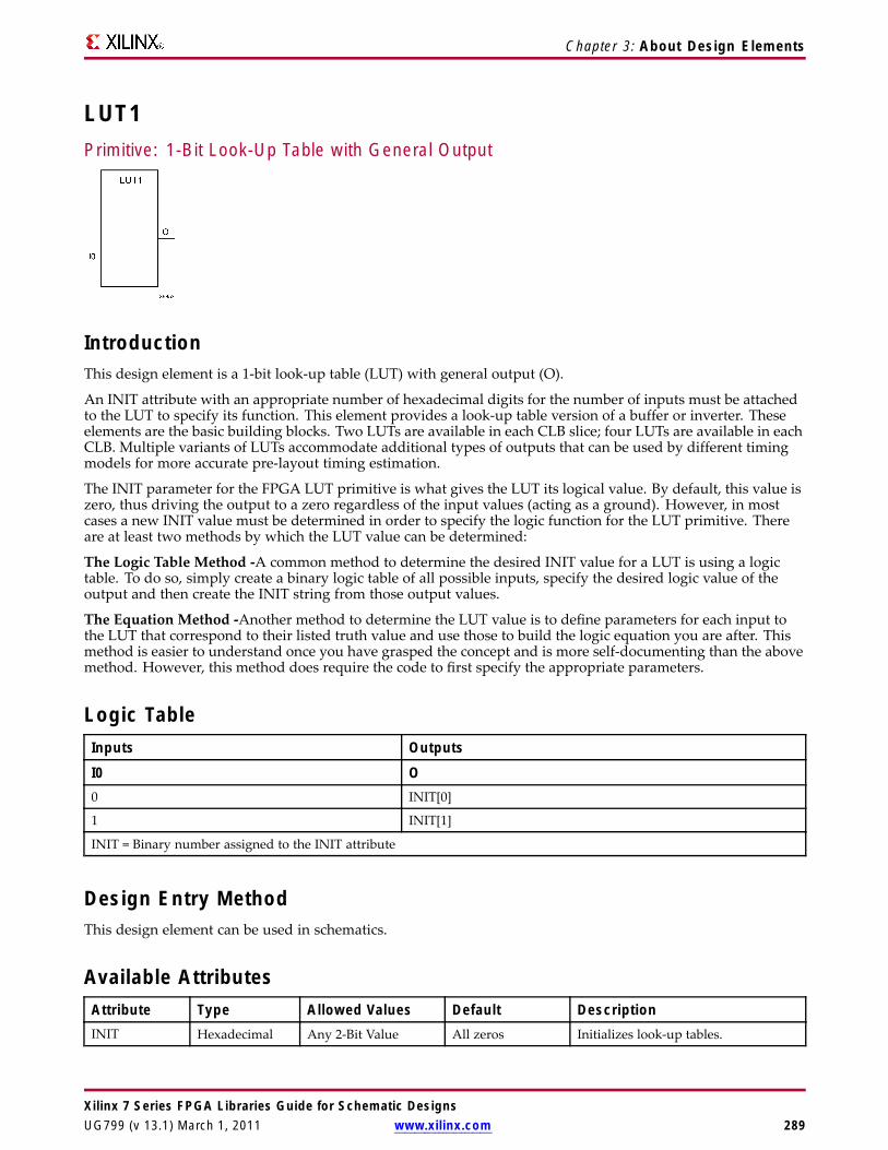
Chapter 3: About Design Elements
LUT1Primitive: 1-Bit Look-Up Table with General Output
IntroductionThis design element is a 1-bit look-up table (LUT) with general output (O).
An INIT attribute with an appropriate number of hexadecimal digits for the number of inputs must be attachedto the LUT to specify its function. This element provides a look-up table version of a buffer or inverter. Theseelements are the basic building blocks. Two LUTs are available in each CLB slice; four LUTs are available in eachCLB. Multiple variants of LUTs accommodate additional types of outputs that can be used by different timingmodels for more accurate pre-layout timing estimation.
The INIT parameter for the FPGA LUT primitive is what gives the LUT its logical value. By default, this value iszero, thus driving the output to a zero regardless of the input values (acting as a ground). However, in mostcases a new INIT value must be determined in order to specify the logic function for the LUT primitive. Thereare at least two methods by which the LUT value can be determined:
The Logic Table Method -A common method to determine the desired INIT value for a LUT is using a logictable. To do so, simply create a binary logic table of all possible inputs, specify the desired logic value of theoutput and then create the INIT string from those output values.
The Equation Method -Another method to determine the LUT value is to define parameters for each input tothe LUT that correspond to their listed truth value and use those to build the logic equation you are after. Thismethod is easier to understand once you have grasped the concept and is more self-documenting than the abovemethod. However, this method does require the code to first specify the appropriate parameters.
Logic TableInputs Outputs
I0 O0 INIT[0]
1 INIT[1]
INIT = Binary number assigned to the INIT attribute
Design Entry MethodThis design element can be used in schematics.
Available AttributesAttribute Type Allowed Values Default DescriptionINIT Hexadecimal Any 2-Bit Value All zeros Initializes look-up tables.
Xilinx 7 Series FPGA Libraries Guide for Schematic DesignsUG799 (v 13.1) March 1, 2011 www.xilinx.com 289

Chapter 3: About Design Elements
For More InformationSee the 7 series FPGA User Documentation (User Guides and Data Sheets).
Xilinx 7 Series FPGA Libraries Guide for Schematic Designs290 www.xilinx.com UG799 (v 13.1) March 1, 2011

Chapter 3: About Design Elements
LUT1_DPrimitive: 1-Bit Look-Up Table with Dual Output
IntroductionThis design element is a 1-bit look-up table (LUT) with two functionally identical outputs, O and LO. It providesa look-up table version of a buffer or inverter.
The O output is a general interconnect. The LO output is used to connect to another output within the same CLBslice and to the fast connect buffer. A mandatory INIT attribute, with an appropriate number of hexadecimaldigits for the number of inputs, must be attached to the LUT to specify its function.
The INIT parameter for the FPGA LUT primitive is what gives the LUT its logical value. By default, this value iszero, thus driving the output to a zero regardless of the input values (acting as a ground). However, in mostcases a new INIT value must be determined in order to specify the logic function for the LUT primitive. Thereare at least two methods by which the LUT value can be determined:
The Logic Table Method -A common method to determine the desired INIT value for a LUT is using a logictable. To do so, simply create a binary logic table of all possible inputs, specify the desired logic value of theoutput and then create the INIT string from those output values.
The Equation Method -Another method to determine the LUT value is to define parameters for each input tothe LUT that correspond to their listed truth value and use those to build the logic equation you are after. Thismethod is easier to understand once you have grasped the concept and is more self-documenting than the abovemethod. However, this method does require the code to first specify the appropriate parameters.
Logic TableInputs Outputs
I0 O LO0 INIT[0] INIT[0]
1 INIT[1] INIT[1]
INIT = Binary number assigned to the INIT attribute
Design Entry MethodThis design element can be used in schematics.
Available AttributesAttribute Type Allowed Values Default DescriptionINIT Hexadecimal Any 2-Bit Value All zeros Initializes look-up tables.
For More InformationSee the 7 series FPGA User Documentation (User Guides and Data Sheets).
Xilinx 7 Series FPGA Libraries Guide for Schematic DesignsUG799 (v 13.1) March 1, 2011 www.xilinx.com 291
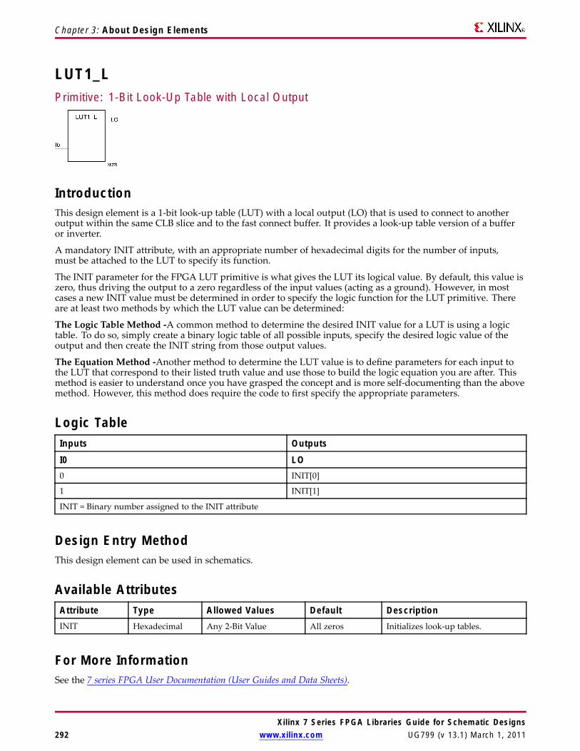
Chapter 3: About Design Elements
LUT1_LPrimitive: 1-Bit Look-Up Table with Local Output
IntroductionThis design element is a 1-bit look-up table (LUT) with a local output (LO) that is used to connect to anotheroutput within the same CLB slice and to the fast connect buffer. It provides a look-up table version of a bufferor inverter.
A mandatory INIT attribute, with an appropriate number of hexadecimal digits for the number of inputs,must be attached to the LUT to specify its function.
The INIT parameter for the FPGA LUT primitive is what gives the LUT its logical value. By default, this value iszero, thus driving the output to a zero regardless of the input values (acting as a ground). However, in mostcases a new INIT value must be determined in order to specify the logic function for the LUT primitive. Thereare at least two methods by which the LUT value can be determined:
The Logic Table Method -A common method to determine the desired INIT value for a LUT is using a logictable. To do so, simply create a binary logic table of all possible inputs, specify the desired logic value of theoutput and then create the INIT string from those output values.
The Equation Method -Another method to determine the LUT value is to define parameters for each input tothe LUT that correspond to their listed truth value and use those to build the logic equation you are after. Thismethod is easier to understand once you have grasped the concept and is more self-documenting than the abovemethod. However, this method does require the code to first specify the appropriate parameters.
Logic TableInputs Outputs
I0 LO0 INIT[0]
1 INIT[1]
INIT = Binary number assigned to the INIT attribute
Design Entry MethodThis design element can be used in schematics.
Available AttributesAttribute Type Allowed Values Default DescriptionINIT Hexadecimal Any 2-Bit Value All zeros Initializes look-up tables.
For More InformationSee the 7 series FPGA User Documentation (User Guides and Data Sheets).
Xilinx 7 Series FPGA Libraries Guide for Schematic Designs292 www.xilinx.com UG799 (v 13.1) March 1, 2011

Chapter 3: About Design Elements
LUT2Primitive: 2-Bit Look-Up Table with General Output
IntroductionThis design element is a 2-bit look-up table (LUT) with general output (O).
An INIT attribute with an appropriate number of hexadecimal digits for the number of inputs must be attachedto the LUT to specify its function. This element provides a look-up table version of a buffer or inverter. Theseelements are the basic building blocks. Two LUTs are available in each CLB slice; four LUTs are available in eachCLB. Multiple variants of LUTs accommodate additional types of outputs that can be used by different timingmodels for more accurate pre-layout timing estimation.
The INIT parameter for the FPGA LUT primitive is what gives the LUT its logical value. By default, this value iszero, thus driving the output to a zero regardless of the input values (acting as a ground). However, in mostcases a new INIT value must be determined in order to specify the logic function for the LUT primitive. Thereare at least two methods by which the LUT value can be determined:
The Logic Table Method -A common method to determine the desired INIT value for a LUT is using a logictable. To do so, simply create a binary logic table of all possible inputs, specify the desired logic value of theoutput and then create the INIT string from those output values.
The Equation Method -Another method to determine the LUT value is to define parameters for each input tothe LUT that correspond to their listed truth value and use those to build the logic equation you are after. Thismethod is easier to understand once you have grasped the concept and is more self-documenting than the abovemethod. However, this method does require the code to first specify the appropriate parameters.
Logic TableInputs Outputs
I1 I0 O0 0 INIT[0]
0 1 INIT[1]
1 0 INIT[2]
1 1 INIT[3]
INIT = Binary equivalent of the hexadecimal number assigned to the INIT attribute
Design Entry MethodThis design element can be used in schematics.
Available AttributesAttribute Type Allowed Values Default DescriptionINIT Hexadecimal Any 4-Bit Value All zeros Initializes look-up tables.
Xilinx 7 Series FPGA Libraries Guide for Schematic DesignsUG799 (v 13.1) March 1, 2011 www.xilinx.com 293

Chapter 3: About Design Elements
For More InformationSee the 7 series FPGA User Documentation (User Guides and Data Sheets).
Xilinx 7 Series FPGA Libraries Guide for Schematic Designs294 www.xilinx.com UG799 (v 13.1) March 1, 2011

Chapter 3: About Design Elements
LUT2_DPrimitive: 2-Bit Look-Up Table with Dual Output
IntroductionThis design element is a 2-bit look-up table (LUT) with two functionally identical outputs, O and LO.
The O output is a general interconnect. The LO output is used to connect to another output within the same CLBslice and to the fast connect buffer. A mandatory INIT attribute, with an appropriate number of hexadecimaldigits for the number of inputs, must be attached to the LUT to specify its function.
The INIT parameter for the FPGA LUT primitive is what gives the LUT its logical value. By default, this value iszero, thus driving the output to a zero regardless of the input values (acting as a ground). However, in mostcases a new INIT value must be determined in order to specify the logic function for the LUT primitive. Thereare at least two methods by which the LUT value can be determined:
The LogicTable Method -A common method to determine the desired INIT value for a LUT is using a logictable. To do so, simply create a binary logic table of all possible inputs, specify the desired logic value of theoutput and then create the INIT string from those output values.
The Equation Method -Another method to determine the LUT value is to define parameters for each input tothe LUT that correspond to their listed truth value and use those to build the logic equation you are after. Thismethod is easier to understand once you have grasped the concept and is more self-documenting than the abovemethod. However, this method does require the code to first specify the appropriate parameters.
Logic TableInputs Outputs
I1 I0 O LO0 0 INIT[0] INIT[0]
0 1 INIT[1] INIT[1]
1 0 INIT[2] INIT[2]
1 1 INIT[3] INIT[3]
INIT = Binary equivalent of the hexadecimal number assigned to the INIT attribute
Design Entry MethodThis design element can be used in schematics.
Available AttributesAttribute Type Allowed Values Default DescriptionINIT Hexadecimal Any 4-Bit Value All zeros Initializes look-up tables.
For More InformationSee the 7 series FPGA User Documentation (User Guides and Data Sheets).
Xilinx 7 Series FPGA Libraries Guide for Schematic DesignsUG799 (v 13.1) March 1, 2011 www.xilinx.com 295

Chapter 3: About Design Elements
LUT2_LPrimitive: 2-Bit Look-Up Table with Local Output
IntroductionThis design element is a 2-bit look-up table (LUT) with a local output (LO) that is used to connect to anotheroutput within the same CLB slice and to the fast connect buffer. It provides a look-up table version of a bufferor inverter.
A mandatory INIT attribute, with an appropriate number of hexadecimal digits for the number of inputs,must be attached to the LUT to specify its function.
The INIT parameter for the FPGA LUT primitive is what gives the LUT its logical value. By default, this value iszero, thus driving the output to a zero regardless of the input values (acting as a ground). However, in mostcases a new INIT value must be determined in order to specify the logic function for the LUT primitive. Thereare at least two methods by which the LUT value can be determined:
The Logic Table Method -A common method to determine the desired INIT value for a LUT is using a logictable. To do so, simply create a binary logic table of all possible inputs, specify the desired logic value of theoutput and then create the INIT string from those output values.
The Equation Method -Another method to determine the LUT value is to define parameters for each input tothe LUT that correspond to their listed truth value and use those to build the logic equation you are after. Thismethod is easier to understand once you have grasped the concept and is more self-documenting than the abovemethod. However, this method does require the code to first specify the appropriate parameters.
Logic TableInputs Outputs
I1 I0 LO0 0 INIT[0]
0 1 INIT[1]
1 0 INIT[2]
1 1 INIT[3]
INIT = Binary equivalent of the hexadecimal number assigned to the INIT attribute
Design Entry MethodThis design element can be used in schematics.
Available AttributesAttribute Type Allowed Values Default DescriptionINIT Hexadecimal Any 4-Bit Value All zeros Initializes look-up tables.
Xilinx 7 Series FPGA Libraries Guide for Schematic Designs296 www.xilinx.com UG799 (v 13.1) March 1, 2011

Chapter 3: About Design Elements
For More InformationSee the 7 series FPGA User Documentation (User Guides and Data Sheets).
Xilinx 7 Series FPGA Libraries Guide for Schematic DesignsUG799 (v 13.1) March 1, 2011 www.xilinx.com 297

Chapter 3: About Design Elements
LUT3Primitive: 3-Bit Look-Up Table with General Output
IntroductionThis design element is a 3-bit look-up table (LUT) with general output (O). A mandatory INIT attribute, withan appropriate number of hexadecimal digits for the number of inputs, must be attached to the LUT to specifyits function.
An INIT attribute with an appropriate number of hexadecimal digits for the number of inputs must be attachedto the LUT to specify its function. This element provides a look-up table version of a buffer or inverter. Theseelements are the basic building blocks. Two LUTs are available in each CLB slice; four LUTs are available in eachCLB. Multiple variants of LUTs accommodate additional types of outputs that can be used by different timingmodels for more accurate pre-layout timing estimation.
The INIT parameter for the FPGA LUT primitive is what gives the LUT its logical value. By default, this value iszero, thus driving the output to a zero regardless of the input values (acting as a ground). However, in mostcases a new INIT value must be determined in order to specify the logic function for the LUT primitive. Thereare at least two methods by which the LUT value can be determined:
The Logic Table Method -A common method to determine the desired INIT value for a LUT is using a logictable. To do so, simply create a binary logic table of all possible inputs, specify the desired logic value of theoutput and then create the INIT string from those output values.
The Equation Method -Another method to determine the LUT value is to define parameters for each input tothe LUT that correspond to their listed truth value and use those to build the logic equation you are after. Thismethod is easier to understand once you have grasped the concept and is more self-documenting than the abovemethod. However, this method does require the code to first specify the appropriate parameters.
Logic TableInputs Outputs
I2 I1 I0 O0 0 0 INIT[0]
0 0 1 INIT[1]
0 1 0 INIT[2]
0 1 1 INIT[3]
1 0 0 INIT[4]
1 0 1 INIT[5]
1 1 0 INIT[6]
1 1 1 INIT[7]
INIT = Binary equivalent of the hexadecimal number assigned to the INIT attribute
Design Entry MethodThis design element can be used in schematics.
Xilinx 7 Series FPGA Libraries Guide for Schematic Designs298 www.xilinx.com UG799 (v 13.1) March 1, 2011

Chapter 3: About Design Elements
Available AttributesAttribute Type Allowed Values Default DescriptionINIT Hexadecimal Any 8-Bit Value All zeros Initializes look-up tables.
For More InformationSee the 7 series FPGA User Documentation (User Guides and Data Sheets).
Xilinx 7 Series FPGA Libraries Guide for Schematic DesignsUG799 (v 13.1) March 1, 2011 www.xilinx.com 299
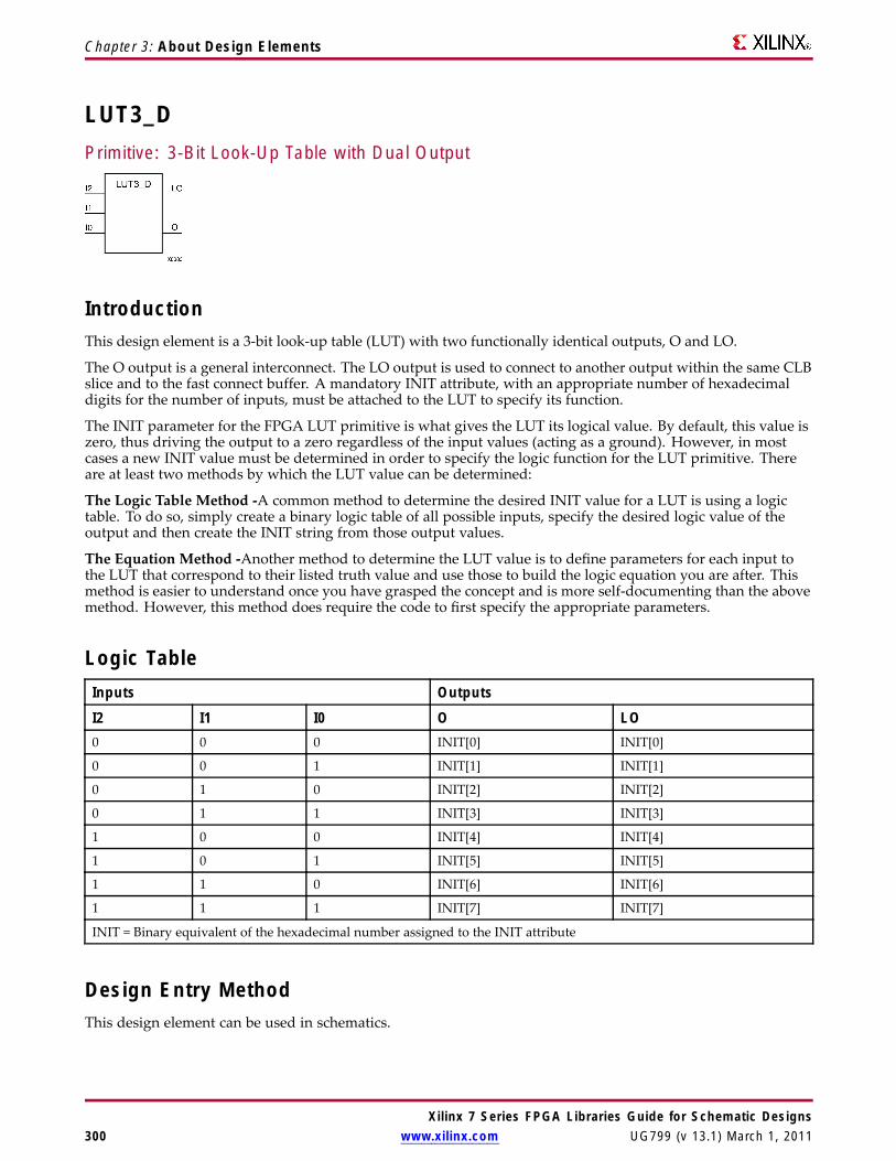
Chapter 3: About Design Elements
LUT3_DPrimitive: 3-Bit Look-Up Table with Dual Output
IntroductionThis design element is a 3-bit look-up table (LUT) with two functionally identical outputs, O and LO.
The O output is a general interconnect. The LO output is used to connect to another output within the same CLBslice and to the fast connect buffer. A mandatory INIT attribute, with an appropriate number of hexadecimaldigits for the number of inputs, must be attached to the LUT to specify its function.
The INIT parameter for the FPGA LUT primitive is what gives the LUT its logical value. By default, this value iszero, thus driving the output to a zero regardless of the input values (acting as a ground). However, in mostcases a new INIT value must be determined in order to specify the logic function for the LUT primitive. Thereare at least two methods by which the LUT value can be determined:
The Logic Table Method -A common method to determine the desired INIT value for a LUT is using a logictable. To do so, simply create a binary logic table of all possible inputs, specify the desired logic value of theoutput and then create the INIT string from those output values.
The Equation Method -Another method to determine the LUT value is to define parameters for each input tothe LUT that correspond to their listed truth value and use those to build the logic equation you are after. Thismethod is easier to understand once you have grasped the concept and is more self-documenting than the abovemethod. However, this method does require the code to first specify the appropriate parameters.
Logic TableInputs Outputs
I2 I1 I0 O LO0 0 0 INIT[0] INIT[0]
0 0 1 INIT[1] INIT[1]
0 1 0 INIT[2] INIT[2]
0 1 1 INIT[3] INIT[3]
1 0 0 INIT[4] INIT[4]
1 0 1 INIT[5] INIT[5]
1 1 0 INIT[6] INIT[6]
1 1 1 INIT[7] INIT[7]
INIT = Binary equivalent of the hexadecimal number assigned to the INIT attribute
Design Entry MethodThis design element can be used in schematics.
Xilinx 7 Series FPGA Libraries Guide for Schematic Designs300 www.xilinx.com UG799 (v 13.1) March 1, 2011

Chapter 3: About Design Elements
Available AttributesAttribute Type Allowed Values Default DescriptionINIT Hexadecimal Any 8-Bit Value All zeros Initializes look-up tables.
For More InformationSee the 7 series FPGA User Documentation (User Guides and Data Sheets).
Xilinx 7 Series FPGA Libraries Guide for Schematic DesignsUG799 (v 13.1) March 1, 2011 www.xilinx.com 301
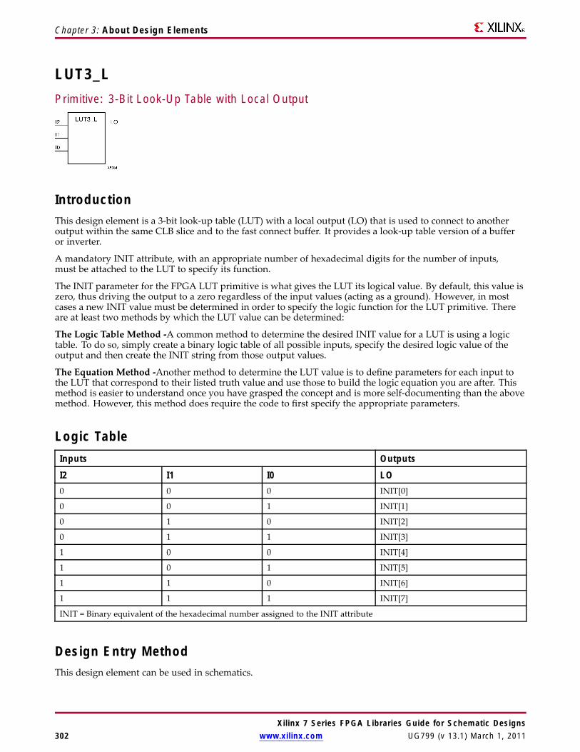
Chapter 3: About Design Elements
LUT3_LPrimitive: 3-Bit Look-Up Table with Local Output
IntroductionThis design element is a 3-bit look-up table (LUT) with a local output (LO) that is used to connect to anotheroutput within the same CLB slice and to the fast connect buffer. It provides a look-up table version of a bufferor inverter.
A mandatory INIT attribute, with an appropriate number of hexadecimal digits for the number of inputs,must be attached to the LUT to specify its function.
The INIT parameter for the FPGA LUT primitive is what gives the LUT its logical value. By default, this value iszero, thus driving the output to a zero regardless of the input values (acting as a ground). However, in mostcases a new INIT value must be determined in order to specify the logic function for the LUT primitive. Thereare at least two methods by which the LUT value can be determined:
The Logic Table Method -A common method to determine the desired INIT value for a LUT is using a logictable. To do so, simply create a binary logic table of all possible inputs, specify the desired logic value of theoutput and then create the INIT string from those output values.
The Equation Method -Another method to determine the LUT value is to define parameters for each input tothe LUT that correspond to their listed truth value and use those to build the logic equation you are after. Thismethod is easier to understand once you have grasped the concept and is more self-documenting than the abovemethod. However, this method does require the code to first specify the appropriate parameters.
Logic TableInputs Outputs
I2 I1 I0 LO0 0 0 INIT[0]
0 0 1 INIT[1]
0 1 0 INIT[2]
0 1 1 INIT[3]
1 0 0 INIT[4]
1 0 1 INIT[5]
1 1 0 INIT[6]
1 1 1 INIT[7]
INIT = Binary equivalent of the hexadecimal number assigned to the INIT attribute
Design Entry MethodThis design element can be used in schematics.
Xilinx 7 Series FPGA Libraries Guide for Schematic Designs302 www.xilinx.com UG799 (v 13.1) March 1, 2011
Chapter 3: About Design Elements
Available AttributesAttribute Type Allowed Values Default DescriptionINIT Hexadecimal Any 8-Bit Value All zeros Initializes look-up tables.
For More InformationSee the 7 series FPGA User Documentation (User Guides and Data Sheets).
Xilinx 7 Series FPGA Libraries Guide for Schematic DesignsUG799 (v 13.1) March 1, 2011 www.xilinx.com 303

Chapter 3: About Design Elements
LUT4Primitive: 4-Bit Look-Up-Table with General Output
IntroductionThis design element is a 4-bit look-up table (LUT) with general output (O).
An INIT attribute with an appropriate number of hexadecimal digits for the number of inputs must be attachedto the LUT to specify its function. This element provides a look-up table version of a buffer or inverter. Theseelements are the basic building blocks. Two LUTs are available in each CLB slice; four LUTs are available in eachCLB. Multiple variants of LUTs accommodate additional types of outputs that can be used by different timingmodels for more accurate pre-layout timing estimation.
The INIT parameter for the FPGA LUT primitive is what gives the LUT its logical value. By default, this value iszero, thus driving the output to a zero regardless of the input values (acting as a ground). However, in mostcases a new INIT value must be determined in order to specify the logic function for the LUT primitive. Thereare at least two methods by which the LUT value can be determined:
The Logic Table Method -A common method to determine the desired INIT value for a LUT is using a logictable. To do so, simply create a binary logic table of all possible inputs, specify the desired logic value of theoutput and then create the INIT string from those output values.
The Equation Method -Another method to determine the LUT value is to define parameters for each input tothe LUT that correspond to their listed truth value and use those to build the logic equation you are after. Thismethod is easier to understand once you have grasped the concept and is more self-documenting than the abovemethod. However, this method does require the code to first specify the appropriate parameters.
Xilinx 7 Series FPGA Libraries Guide for Schematic Designs304 www.xilinx.com UG799 (v 13.1) March 1, 2011

Chapter 3: About Design Elements
Logic TableInputs Outputs
I3 I2 I1 I0 O0 0 0 0 INIT[0]
0 0 0 1 INIT[1]
0 0 1 0 INIT[2]
0 0 1 1 INIT[3]
0 1 0 0 INIT[4]
0 1 0 1 INIT[5]
0 1 1 0 INIT[6]
0 1 1 1 INIT[7]
1 0 0 0 INIT[8]
1 0 0 1 INIT[9]
1 0 1 0 INIT[10]
1 0 1 1 INIT[11]
1 1 0 0 INIT[12]
1 1 0 1 INIT[13]
1 1 1 0 INIT[14]
1 1 1 1 INIT[15]
INIT = Binary equivalent of the hexadecimal number assigned to the INIT attribute
Design Entry MethodThis design element can be used in schematics.
Available AttributesAttribute Type Allowed Values Default DescriptionINIT Hexadecimal Any 16-Bit Value All zeros Initializes look-up tables.
For More InformationSee the 7 series FPGA User Documentation (User Guides and Data Sheets).
Xilinx 7 Series FPGA Libraries Guide for Schematic DesignsUG799 (v 13.1) March 1, 2011 www.xilinx.com 305

Chapter 3: About Design Elements
LUT4_DPrimitive: 4-Bit Look-Up Table with Dual Output
IntroductionThis design element is a 4-bit look-up table (LUT) with two functionally identical outputs, O and LO
The O output is a general interconnect. The LO output is used to connect to another output within the same CLBslice and to the fast connect buffer. A mandatory INIT attribute, with an appropriate number of hexadecimaldigits for the number of inputs, must be attached to the LUT to specify its function.
The INIT parameter for the FPGA LUT primitive is what gives the LUT its logical value. By default, this value iszero, thus driving the output to a zero regardless of the input values (acting as a ground). However, in mostcases a new INIT value must be determined in order to specify the logic function for the LUT primitive. Thereare at least two methods by which the LUT value can be determined:
The Logic Table Method -A common method to determine the desired INIT value for a LUT is using a logictable. To do so, simply create a binary logic table of all possible inputs, specify the desired logic value of theoutput and then create the INIT string from those output values.
The Equation Method -Another method to determine the LUT value is to define parameters for each input tothe LUT that correspond to their listed truth value and use those to build the logic equation you are after. Thismethod is easier to understand once you have grasped the concept and is more self-documenting than the abovemethod. However, this method does require the code to first specify the appropriate parameters.
Xilinx 7 Series FPGA Libraries Guide for Schematic Designs306 www.xilinx.com UG799 (v 13.1) March 1, 2011
Chapter 3: About Design Elements
Logic TableInputs Outputs
I3 I2 I1 I0 O LO0 0 0 0 INIT[0] INIT[0]
0 0 0 1 INIT[1] INIT[1]
0 0 1 0 INIT[2] INIT[2]
0 0 1 1 INIT[3] INIT[3]
0 1 0 0 INIT[4] INIT[4]
0 1 0 1 INIT[5] INIT[5]
0 1 1 0 INIT[6] INIT[6]
0 1 1 1 INIT[7] INIT[7]
1 0 0 0 INIT[8] INIT[8]
1 0 0 1 INIT[9] INIT[9]
1 0 1 0 INIT[10] INIT[10]
1 0 1 1 INIT[11] INIT[11]
1 1 0 0 INIT[12] INIT[12]
1 1 0 1 INIT[13] INIT[13]
1 1 1 0 INIT[14] INIT[14]
1 1 1 1 INIT[15] INIT[15]
INIT = Binary equivalent of the hexadecimal number assigned to the INIT attribute
Design Entry MethodThis design element can be used in schematics.
Available AttributesAttribute Type Allowed Values Default DescriptionINIT Hexadecimal Any 16-Bit Value All zeros Initializes look-up tables.
For More InformationSee the 7 series FPGA User Documentation (User Guides and Data Sheets).
Xilinx 7 Series FPGA Libraries Guide for Schematic DesignsUG799 (v 13.1) March 1, 2011 www.xilinx.com 307

Chapter 3: About Design Elements
LUT4_LPrimitive: 4-Bit Look-Up Table with Local Output
IntroductionThis design element is a 4-bit look-up table (LUT) with a local output (LO) that is used to connect to anotheroutput within the same CLB slice and to the fast connect buffer. It provides a look-up table version of a bufferor inverter.
A mandatory INIT attribute, with an appropriate number of hexadecimal digits for the number of inputs,must be attached to the LUT to specify its function.
The INIT parameter for the FPGA LUT primitive is what gives the LUT its logical value. By default, this value iszero, thus driving the output to a zero regardless of the input values (acting as a ground). However, in mostcases a new INIT value must be determined in order to specify the logic function for the LUT primitive. Thereare at least two methods by which the LUT value can be determined:
The Logic Table Method -A common method to determine the desired INIT value for a LUT is using a logictable. To do so, simply create a binary logic table of all possible inputs, specify the desired logic value of theoutput and then create the INIT string from those output values.
The Equation Method -Another method to determine the LUT value is to define parameters for each input tothe LUT that correspond to their listed truth value and use those to build the logic equation you are after. Thismethod is easier to understand once you have grasped the concept and more self-documenting than the abovemethod. However, this method does require the code to first specify the appropriate parameters.
Xilinx 7 Series FPGA Libraries Guide for Schematic Designs308 www.xilinx.com UG799 (v 13.1) March 1, 2011

Chapter 3: About Design Elements
Logic TableInputs Outputs
I3 I2 I1 I0 LO0 0 0 0 INIT[0]
0 0 0 1 INIT[1]
0 0 1 0 INIT[2]
0 0 1 1 INIT[3]
0 1 0 0 INIT[4]
0 1 0 1 INIT[5]
0 1 1 0 INIT[6]
0 1 1 1 INIT[7]
1 0 0 0 INIT[8]
1 0 0 1 INIT[9]
1 0 1 0 INIT[10]
1 0 1 1 INIT[11]
1 1 0 0 INIT[12]
1 1 0 1 INIT[13]
1 1 1 0 INIT[14]
1 1 1 1 INIT[15]
INIT = Binary equivalent of the hexadecimal number assigned to the INIT attribute
Design Entry MethodThis design element can be used in schematics.
Available AttributesAttribute Type Allowed Values Default DescriptionINIT Hexadecimal Any 16-Bit Value All zeros Initializes look-up tables.
For More InformationSee the 7 series FPGA User Documentation (User Guides and Data Sheets).
Xilinx 7 Series FPGA Libraries Guide for Schematic DesignsUG799 (v 13.1) March 1, 2011 www.xilinx.com 309

Chapter 3: About Design Elements
LUT5Primitive: 5-Input Lookup Table with General Output
IntroductionThis design element is a 5-input, 1-output look-up table (LUT) that can either act as an asynchronous 32-bit ROM(with 5-bit addressing) or implement any 5-input logic function. LUTs are the basic logic building blocks andare used to implement most logic functions of the design. One LUT5 is packed into a LUT6 within a slice, ortwo LUT5s can be packed into a single LUT6 with some restrictions. The functionality of the LUT5, LUT5_Land LUT5_D is the same. However, the LUT5_L and LUT5_D allow the additional specification to connect theLUT5 output signal to an internal slice or CLB connection using the LO output. The LUT5_L specifies thatthe only connections from the LUT5 will be within a slice or CLB, while the LUT5_D allows the specificationto connect the output of the LUT to both inter-slice/CLB logic and external logic as well. The LUT5 does notstate any specific output connections and should be used in all cases except where internal slice or CLB signalconnections must be implicitly specified.
An INIT attribute consisting of a 32-bit hexadecimal value must be specified to indicate the LUTs logical function.The INIT value is calculated by assigning a 1 to the corresponding INIT bit value when the associated inputsare applied. For instance, a Verilog INIT value of 32’h80000000 (X"80000000" for VHDL) makes the output zerounless all of the inputs are one (a 5-input AND gate). A Verilog INIT value of 32’hfffffffe (X"FFFFFFFE" forVHDL) makes the output one unless all zeros are on the inputs (a 5-input OR gate).
The INIT parameter for the FPGA LUT primitive is what gives the LUT its logical value. By default, this value iszero, thus driving the output to a zero regardless of the input values (acting as a ground). However, in mostcases a new INIT value must be determined in order to specify the logic function for the LUT primitive. Thereare at least two methods by which the LUT value can be determined:
The Logic Table Method -A common method to determine the desired INIT value for a LUT is using a logictable. To do so, simply create a binary logic table of all possible inputs, specify the desired logic value of theoutput and then create the INIT string from those output values.
The Equation Method -Another method to determine the LUT value is to define parameters for each input tothe LUT that correspond to their listed truth value and use those to build the logic equation you are after. Thismethod is easier to understand once you have grasped the concept and is more self-documenting than the abovemethod. However, this method does require the code to first specify the appropriate parameters.
Xilinx 7 Series FPGA Libraries Guide for Schematic Designs310 www.xilinx.com UG799 (v 13.1) March 1, 2011

Chapter 3: About Design Elements
Logic TableInputs Outputs
I4 I3 I2 I1 I0 LO0 0 0 0 0 INIT[0]
0 0 0 0 1 INIT[1]
0 0 0 1 0 INIT[2]
0 0 0 1 1 INIT[3]
0 0 1 0 0 INIT[4]
0 0 1 0 1 INIT[5]
0 0 1 1 0 INIT[6]
0 0 1 1 1 INIT[7]
0 1 0 0 0 INIT[8]
0 1 0 0 1 INIT[9]
0 1 0 1 0 INIT[10]
0 1 0 1 1 INIT[11]
0 1 1 0 0 INIT[12]
0 1 1 0 1 INIT[13]
0 1 1 1 0 INIT[14]
0 1 1 1 1 INIT[15]
1 0 0 0 0 INIT[16]
1 0 0 0 1 INIT[17]
1 0 0 1 0 INIT[18]
1 0 0 1 1 INIT[19]
1 0 1 0 0 INIT[20]
1 0 1 0 1 INIT[21]
1 0 1 1 0 INIT[22]
1 0 1 1 1 INIT[23]
1 1 0 0 0 INIT[24]
1 1 0 0 1 INIT[25]
1 1 0 1 0 INIT[26]
1 1 0 1 1 INIT[27]
1 1 1 0 0 INIT[28]
1 1 1 0 1 INIT[29]
1 1 1 1 0 INIT[30]
1 1 1 1 1 INIT[31]
INIT = Binary equivalent of the hexadecimal number assigned to the INIT attribute
Xilinx 7 Series FPGA Libraries Guide for Schematic DesignsUG799 (v 13.1) March 1, 2011 www.xilinx.com 311
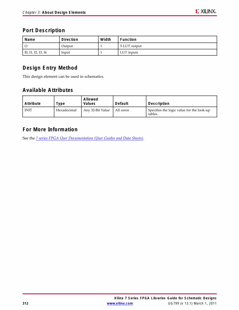
Chapter 3: About Design Elements
Port DescriptionName Direction Width FunctionO Output 1 5-LUT output
I0, I1, I2, I3, I4 Input 1 LUT inputs
Design Entry MethodThis design element can be used in schematics.
Available Attributes
Attribute TypeAllowedValues Default Description
INIT Hexadecimal Any 32-Bit Value All zeros Specifies the logic value for the look-uptables.
For More InformationSee the 7 series FPGA User Documentation (User Guides and Data Sheets).
Xilinx 7 Series FPGA Libraries Guide for Schematic Designs312 www.xilinx.com UG799 (v 13.1) March 1, 2011

Chapter 3: About Design Elements
LUT5_DPrimitive: 5-Input Lookup Table with General and Local Outputs
IntroductionThis design element is a 5-input, 1-output look-up table (LUT) that can either act as an asynchronous 32-bit ROM(with 5-bit addressing) or implement any 5-input logic function. LUTs are the basic logic building blocks and areused to implement most logic functions of the design. One LUT5 will be packed into a LUT6 within a slice, ortwo LUT5s can be packed into a single LUT6 with some restrictions. The functionality of the LUT5, LUT5_Land LUT5_D is the same. However, the LUT5_L and LUT5_D allow the additional specification to connect theLUT5 output signal to an internal slice or CLB connection using the LO output. The LUT5_L specifies thatthe only connections from the LUT5 will be within a slice or CLB, while the LUT5_D allows the specificationto connect the output of the LUT to both inter-slice/CLB logic and external logic as well. The LUT5 does notstate any specific output connections and should be used in all cases except where internal slice or CLB signalconnections must be implicitly specified.
An INIT attribute consisting of a 32-bit hexadecimal value must be specified to indicate the LUTs logical function.The INIT value is calculated by assigning a 1 to the corresponding INIT bit value when the associated inputsare applied. For instance, a Verilog INIT value of 32’h80000000 (X"80000000" for VHDL) will make the outputzero unless all of the inputs are one (a 5-input AND gate). A Verilog INIT value of 32’hfffffffe (X"FFFFFFFE" forVHDL) will make the output one unless all zeros are on the inputs (a 5-input OR gate).
The INIT parameter for the FPGA LUT primitive is what gives the LUT its logical value. By default, this value iszero, thus driving the output to a zero regardless of the input values (acting as a ground). However, in mostcases a new INIT value must be determined in order to specify the logic function for the LUT primitive. Thereare at least two methods by which the LUT value can be determined:
The Logic Table Method -A common method to determine the desired INIT value for a LUT is using a logictable. To do so, simply create a binary logic table of all possible inputs, specify the desired logic value of theoutput and then create the INIT string from those output values.
The Equation Method -Another method to determine the LUT value is to define parameters for each input tothe LUT that correspond to their listed truth value and use those to build the logic equation you are after. Thismethod is easier to understand once you have grasped the concept and more self-documenting that the abovemethod. However, this method does require the code to first specify the appropriate parameters.
Xilinx 7 Series FPGA Libraries Guide for Schematic DesignsUG799 (v 13.1) March 1, 2011 www.xilinx.com 313

Chapter 3: About Design Elements
Logic TableInputs Outputs
I4 I3 I2 I1 I0 O LO0 0 0 0 0 INIT[0] INIT[0]
0 0 0 0 1 INIT[1] INIT[1]
0 0 0 1 0 INIT[2] INIT[2]
0 0 0 1 1 INIT[3] INIT[3]
0 0 1 0 0 INIT[4] INIT[4]
0 0 1 0 1 INIT[5] INIT[5]
0 0 1 1 0 INIT[6] INIT[6]
0 0 1 1 1 INIT[7] INIT[7]
0 1 0 0 0 INIT[8] INIT[8]
0 1 0 0 1 INIT[9] INIT[9]
0 1 0 1 0 INIT[10] INIT[10]
0 1 0 1 1 INIT[11] INIT[11]
0 1 1 0 0 INIT[12] INIT[12]
0 1 1 0 1 INIT[13] INIT[13]
0 1 1 1 0 INIT[14] INIT[14]
0 1 1 1 1 INIT[15] INIT[15]
1 0 0 0 0 INIT[16] INIT[16]
1 0 0 0 1 INIT[17] INIT[17]
1 0 0 1 0 INIT[18] INIT[18]
1 0 0 1 1 INIT[19] INIT[19]
1 0 1 0 0 INIT[20] INIT[20]
1 0 1 0 1 INIT[21] INIT[21]
1 0 1 1 0 INIT[22] INIT[22]
1 0 1 1 1 INIT[23] INIT[23]
1 1 0 0 0 INIT[24] INIT[24]
1 1 0 0 1 INIT[25] INIT[25]
1 1 0 1 0 INIT[26] INIT[26]
1 1 0 1 1 INIT[27] INIT[27]
1 1 1 0 0 INIT[28] INIT[28]
1 1 1 0 1 INIT[29] INIT[29]
1 1 1 1 0 INIT[30] INIT[30]
1 1 1 1 1 INIT[31] INIT[31]
INIT = Binary equivalent of the hexadecimal number assigned to the INIT attribute
Xilinx 7 Series FPGA Libraries Guide for Schematic Designs314 www.xilinx.com UG799 (v 13.1) March 1, 2011

Chapter 3: About Design Elements
Port DescriptionName Direction Width FunctionO Output 1 5-LUT output
L0 Output 1 5-LUT output for internal CLB connection
I0, I1, I2, I3, I4 Input 1 LUT inputs
Design Entry MethodThis design element can be used in schematics.
Available Attributes
Attribute TypeAllowedValues Default Description
INIT Hexadecimal Any 32-Bit Value All zeros Specifies the logic value for the look-uptables.
For More InformationSee the 7 series FPGA User Documentation (User Guides and Data Sheets).
Xilinx 7 Series FPGA Libraries Guide for Schematic DesignsUG799 (v 13.1) March 1, 2011 www.xilinx.com 315

Chapter 3: About Design Elements
LUT5_LPrimitive: 5-Input Lookup Table with Local Output
IntroductionThis design element is a 5-input, 1-output look-up table (LUT) that can either act as an asynchronous 32-bit ROM(with 5-bit addressing) or implement any 5-input logic function. LUTs are the basic logic building blocks and areused to implement most logic functions of the design. One LUT5 will be packed into a LUT6 within a slice, ortwo LUT5s can be packed into a single LUT6 with some restrictions. The functionality of the LUT5, LUT5_Land LUT5_D is the same. However, the LUT5_L and LUT5_D allow the additional specification to connectthe LUT5 output signal to an internal slice or CLB connection using the LO output. The LUT5_L specifiesthat the only connections from the LUT5 is within a slice or CLB, while the LUT5_D allows the specificationto connect the output of the LUT to both inter-slice/CLB logic and external logic as well. The LUT5 does notstate any specific output connections and should be used in all cases except where internal slice or CLB signalconnections must be implicitly specified.
An INIT attribute consisting of a 32-bit hexadecimal value must be specified to indicate the LUTs logical function.The INIT value is calculated by assigning a 1 to the corresponding INIT bit value when the associated inputsare applied. For instance, a Verilog INIT value of 32’h80000000 (X"80000000" for VHDL) makes the output zerounless all of the inputs are one (a 5-input AND gate). A Verilog INIT value of 32’hfffffffe (X"FFFFFFFE" forVHDL) makes the output one unless all zeros are on the inputs (a 5-input OR gate).
The INIT parameter for the FPGA LUT primitive is what gives the LUT its logical value. By default, this value iszero, thus driving the output to a zero regardless of the input values (acting as a ground). However, in mostcases a new INIT value must be determined in order to specify the logic function for the LUT primitive. Thereare at least two methods by which the LUT value can be determined:
The Logic Table Method -A common method to determine the desired INIT value for a LUT is using a logictable. To do so, simply create a binary truth table of all possible inputs, specify the desired logic value of theoutput and then create the INIT string from those output values.
The Equation Method -Another method to determine the LUT value is to define parameters for each input tothe LUT that correspond to their listed logic value and use those to build the logic equation you are after. Thismethod is easier to understand once you have grasped the concept and is more self-documenting than the abovemethod. However, this method does require the code to first specify the appropriate parameters.
Xilinx 7 Series FPGA Libraries Guide for Schematic Designs316 www.xilinx.com UG799 (v 13.1) March 1, 2011

Chapter 3: About Design Elements
Logic TableInputs Outputs
I4 I3 I2 I1 I0 LO0 0 0 0 0 INIT[0]
0 0 0 0 1 INIT[1]
0 0 0 1 0 INIT[2]
0 0 0 1 1 INIT[3]
0 0 1 0 0 INIT[4]
0 0 1 0 1 INIT[5]
0 0 1 1 0 INIT[6]
0 0 1 1 1 INIT[7]
0 1 0 0 0 INIT[8]
0 1 0 0 1 INIT[9]
0 1 0 1 0 INIT[10]
0 1 0 1 1 INIT[11]
0 1 1 0 0 INIT[12]
0 1 1 0 1 INIT[13]
0 1 1 1 0 INIT[14]
0 1 1 1 1 INIT[15]
1 0 0 0 0 INIT[16]
1 0 0 0 1 INIT[17]
1 0 0 1 0 INIT[18]
1 0 0 1 1 INIT[19]
1 0 1 0 0 INIT[20]
1 0 1 0 1 INIT[21]
1 0 1 1 0 INIT[22]
1 0 1 1 1 INIT[23]
1 1 0 0 0 INIT[24]
1 1 0 0 1 INIT[25]
1 1 0 1 0 INIT[26]
1 1 0 1 1 INIT[27]
1 1 1 0 0 INIT[28]
1 1 1 0 1 INIT[29]
1 1 1 1 0 INIT[30]
1 1 1 1 1 INIT[31]
INIT = Binary equivalent of the hexadecimal number assigned to the INIT attribute
Xilinx 7 Series FPGA Libraries Guide for Schematic DesignsUG799 (v 13.1) March 1, 2011 www.xilinx.com 317

Chapter 3: About Design Elements
Port DescriptionName Direction Width FunctionL0 Output 1 6/5-LUT output for internal CLB connection
I0, I1, I2, I3, I4 Input 1 LUT inputs
Design Entry MethodThis design element can be used in schematics.
Available Attributes
Attribute TypeAllowedValues Default Description
INIT Hexadecimal Any 32-Bit Value All zeros Specifies the logic value for the look-uptables.
For More InformationSee the 7 series FPGA User Documentation (User Guides and Data Sheets).
Xilinx 7 Series FPGA Libraries Guide for Schematic Designs318 www.xilinx.com UG799 (v 13.1) March 1, 2011

Chapter 3: About Design Elements
LUT6Primitive: 6-Input Lookup Table with General Output
IntroductionThis design element is a 6-input, 1-output look-up table (LUT) that can either act as an asynchronous 64-bit ROM(with 6-bit addressing) or implement any 6-input logic function. LUTs are the basic logic building blocks and areused to implement most logic functions of the design. A LUT6 is mapped to one of the four look-up tables in theslice. The functionality of the LUT6, LUT6_L and LUT6_D is the same. However, the LUT6_L and LUT6_D allowthe additional specification to connect the LUT6 output signal to an internal slice, or CLB connection, using theLO output. The LUT6_L specifies that the only connections from the LUT6 will be within a slice, or CLB, whilethe LUT6_D allows the specification to connect the output of the LUT to both inter-slice/CLB logic and externallogic as well. The LUT6 does not state any specific output connections and should be used in all cases exceptwhere internal slice or CLB signal connections must be implicitly specified.
An INIT attribute consisting of a 64-bit Hexadecimal value must be specified to indicate the LUTs logical function.The INIT value is calculated by assigning a 1 to corresponding INIT bit value when the associated inputs areapplied. For instance, a Verilog INIT value of 64’h8000000000000000 (X"8000000000000000" for VHDL) makesthe output zero unless all of the inputs are one (a 6-input AND gate). A Verilog INIT value of 64’hfffffffffffffffe(X"FFFFFFFFFFFFFFFE" for VHDL) makes the output one unless all zeros are on the inputs (a 6-input OR gate).
The INIT parameter for the FPGA LUT primitive is what gives the LUT its logical value. By default, this value iszero, thus driving the output to a zero regardless of the input values (acting as a ground). However, in mostcases a new INIT value must be determined in order to specify the logic function for the LUT primitive. Thereare at least two methods by which the LUT value can be determined:
The Logic Table Method -A common method to determine the desired INIT value for a LUT is using a logictable. To do so, simply create a binary logic table of all possible inputs, specify the desired logic value of theoutput and then create the INIT string from those output values.
The Equation Method -Another method to determine the LUT value is to define parameters for each input tothe LUT that correspond to their listed truth value and use those to build the logic equation you are after. Thismethod is easier to understand once you have grasped the concept and is more self-documenting than the abovemethod. However, this method does require the code to first specify the appropriate parameters.
Logic TableInputs Outputs
I5 I4 I3 I2 I1 I0 O0 0 0 0 0 0 INIT[0]
0 0 0 0 0 1 INIT[1]
0 0 0 0 1 0 INIT[2]
0 0 0 0 1 1 INIT[3]
0 0 0 1 0 0 INIT[4]
0 0 0 1 0 1 INIT[5]
0 0 0 1 1 0 INIT[6]
0 0 0 1 1 1 INIT[7]
Xilinx 7 Series FPGA Libraries Guide for Schematic DesignsUG799 (v 13.1) March 1, 2011 www.xilinx.com 319
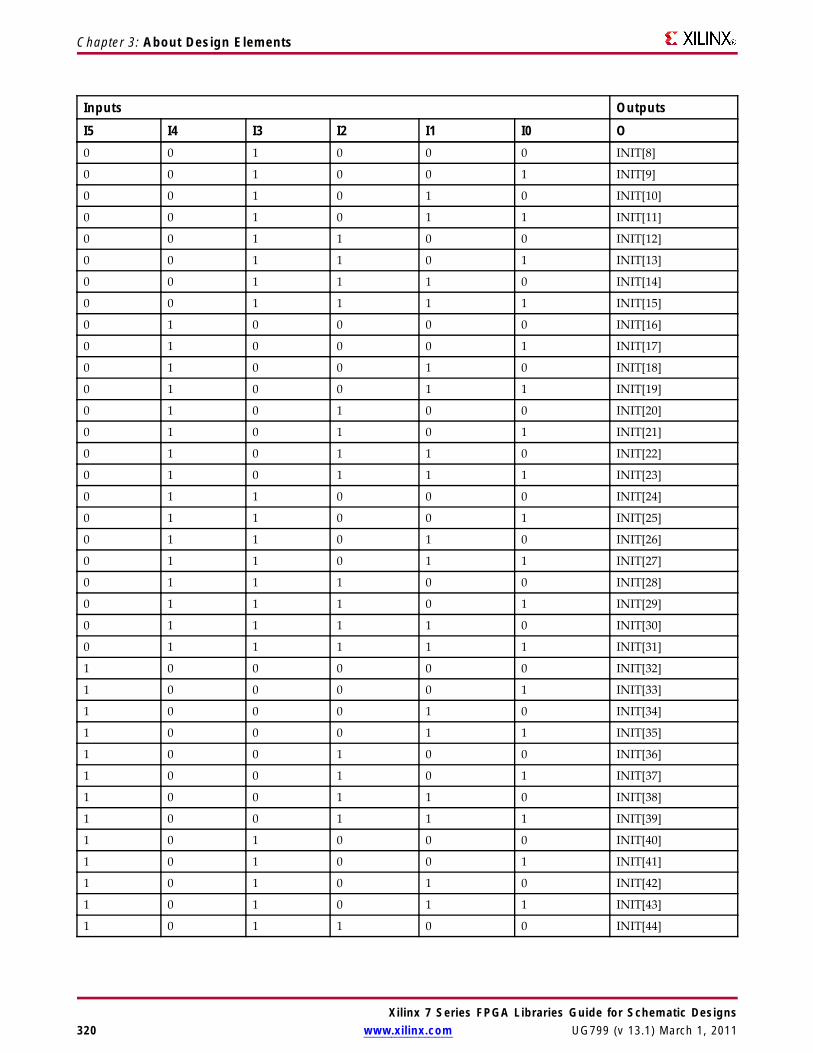
Chapter 3: About Design Elements
Inputs Outputs
I5 I4 I3 I2 I1 I0 O0 0 1 0 0 0 INIT[8]
0 0 1 0 0 1 INIT[9]
0 0 1 0 1 0 INIT[10]
0 0 1 0 1 1 INIT[11]
0 0 1 1 0 0 INIT[12]
0 0 1 1 0 1 INIT[13]
0 0 1 1 1 0 INIT[14]
0 0 1 1 1 1 INIT[15]
0 1 0 0 0 0 INIT[16]
0 1 0 0 0 1 INIT[17]
0 1 0 0 1 0 INIT[18]
0 1 0 0 1 1 INIT[19]
0 1 0 1 0 0 INIT[20]
0 1 0 1 0 1 INIT[21]
0 1 0 1 1 0 INIT[22]
0 1 0 1 1 1 INIT[23]
0 1 1 0 0 0 INIT[24]
0 1 1 0 0 1 INIT[25]
0 1 1 0 1 0 INIT[26]
0 1 1 0 1 1 INIT[27]
0 1 1 1 0 0 INIT[28]
0 1 1 1 0 1 INIT[29]
0 1 1 1 1 0 INIT[30]
0 1 1 1 1 1 INIT[31]
1 0 0 0 0 0 INIT[32]
1 0 0 0 0 1 INIT[33]
1 0 0 0 1 0 INIT[34]
1 0 0 0 1 1 INIT[35]
1 0 0 1 0 0 INIT[36]
1 0 0 1 0 1 INIT[37]
1 0 0 1 1 0 INIT[38]
1 0 0 1 1 1 INIT[39]
1 0 1 0 0 0 INIT[40]
1 0 1 0 0 1 INIT[41]
1 0 1 0 1 0 INIT[42]
1 0 1 0 1 1 INIT[43]
1 0 1 1 0 0 INIT[44]
Xilinx 7 Series FPGA Libraries Guide for Schematic Designs320 www.xilinx.com UG799 (v 13.1) March 1, 2011

Chapter 3: About Design Elements
Inputs Outputs
I5 I4 I3 I2 I1 I0 O1 0 1 1 0 1 INIT[45]
1 0 1 1 1 0 INIT[46]
1 0 1 1 1 1 INIT[47]
1 1 0 0 0 0 INIT[48]
1 1 0 0 0 1 INIT[49]
1 1 0 0 1 0 INIT[50]
1 1 0 0 1 1 INIT[51]
1 1 0 1 0 0 INIT[52]
1 1 0 1 0 1 INIT[53]
1 1 0 1 1 0 INIT[54]
1 1 0 1 1 1 INIT[55]
1 1 1 0 0 0 INIT[56]
1 1 1 0 0 1 INIT[57]
1 1 1 0 1 0 INIT[58]
1 1 1 0 1 1 INIT[59]
1 1 1 1 0 0 INIT[60]
1 1 1 1 0 1 INIT[61]
1 1 1 1 1 0 INIT[62]
1 1 1 1 1 1 INIT[63]
INIT = Binary equivalent of the hexadecimal number assigned to the INIT attribute
Port DescriptionName Direction Width FunctionO Output 1 6/5-LUT output
I0, I1, I2, I3, I4, I5 Input 1 LUT inputs
Design Entry MethodThis design element can be used in schematics.
Available AttributesAttribute Type Allowed Values Default DescriptionINIT Hexadecimal Any 64-Bit Value All zeros Specifies the logic value for the
look-up tables.
For More InformationSee the 7 series FPGA User Documentation (User Guides and Data Sheets).
Xilinx 7 Series FPGA Libraries Guide for Schematic DesignsUG799 (v 13.1) March 1, 2011 www.xilinx.com 321

Chapter 3: About Design Elements
LUT6_2Primitive: Six-input, 2-output, Look-Up Table
IntroductionThis design element is a 6-input, 2-output look-up table (LUT) that can either act as a dual asynchronous 32-bitROM (with 5-bit addressing), implement any two 5-input logic functions with shared inputs, or implement a6-input logic function and a 5-input logic function with shared inputs and shared logic values. LUTs are thebasic logic building blocks and are used to implement most logic functions of the design. A LUT6_2 will bemapped to one of the four look-up tables in the slice.
An INIT attribute consisting of a 64-bit hexadecimal value must be specified to indicate the LUTs logical function.The INIT value is calculated by assigning a 1 to corresponding INIT bit value when the associated inputs areapplied. For instance, a Verilog INIT value of 64’hfffffffffffffffe (X"FFFFFFFFFFFFFFFE" for VHDL) makes the O6output 1 unless all zeros are on the inputs and the O5 output a 1, or unless I[4:0] are all zeroes (a 5-input and6-input OR gate). The lower half (bits 31:0) of the INIT values apply to the logic function of the O5 output.
The INIT parameter for the FPGA LUT primitive is what gives the LUT its logical value. By default, this value iszero, thus driving the output to a zero regardless of the input values (acting as a ground). However, in mostcases a new INIT value must be determined in order to specify the logic function for the LUT primitive. Thereare at least two methods by which the LUT value can be determined:
The Logic Table Method -A common method to determine the desired INIT value for a LUT is using a logictable. To do so, simply create a binary logic table of all possible inputs, specify the desired logic value of theoutput and then create the INIT string from those output values.
The Equation Method -Another method to determine the LUT value is to define parameters for each input tothe LUT that correspond to their listed truth value and use those to build the logic equation you are after. Thismethod is easier to understand once you have grasped the concept and is more self-documenting than the abovemethod. However, this method does require the code to first specify the appropriate parameters.
Logic TableInputs OutputsI5 I4 I3 I2 I1 I0 O5 O6
0 0 0 0 0 0 INIT[0] INIT[0]
0 0 0 0 0 1 INIT[1] INIT[1]
0 0 0 0 1 0 INIT[2] INIT[2]
0 0 0 0 1 1 INIT[3] INIT[3]
0 0 0 1 0 0 INIT[4] INIT[4]
0 0 0 1 0 1 INIT[5] INIT[5]
0 0 0 1 1 0 INIT[6] INIT[6]
0 0 0 1 1 1 INIT[7] INIT[7]
Xilinx 7 Series FPGA Libraries Guide for Schematic Designs322 www.xilinx.com UG799 (v 13.1) March 1, 2011

Chapter 3: About Design Elements
Inputs Outputs0 0 1 0 0 0 INIT[8] INIT[8]
0 0 1 0 0 1 INIT[9] INIT[9]
0 0 1 0 1 0 INIT[10] INIT[10]
0 0 1 0 1 1 INIT[11] INIT[11]
0 0 1 1 0 0 INIT[12] INIT[12]
0 0 1 1 0 1 INIT[13] INIT[13]
0 0 1 1 1 0 INIT[14] INIT[14]
0 0 1 1 1 1 INIT[15] INIT[15]
0 1 0 0 0 0 INIT[16] INIT[16]
0 1 0 0 0 1 INIT[17] INIT[17]
0 1 0 0 1 0 INIT[18] INIT[18]
0 1 0 0 1 1 INIT[19] INIT[19]
0 1 0 1 0 0 INIT[20] INIT[20]
0 1 0 1 0 1 INIT[21] INIT[21]
0 1 0 1 1 0 INIT[22] INIT[22]
0 1 0 1 1 1 INIT[23] INIT[23]
0 1 1 0 0 0 INIT[24] INIT[24]
0 1 1 0 0 1 INIT[25] INIT[25]
0 1 1 0 1 0 INIT[26] INIT[26]
0 1 1 0 1 1 INIT[27] INIT[27]
0 1 1 1 0 0 INIT[28] INIT[28]
0 1 1 1 0 1 INIT[29] INIT[29]
0 1 1 1 1 0 INIT[30] INIT[30]
0 1 1 1 1 1 INIT[31] INIT[31]
1 0 0 0 0 0 INIT[0] INIT[32]
1 0 0 0 0 1 INIT[1] INIT[33]
1 0 0 0 1 0 INIT[2] INIT[34]
1 0 0 0 1 1 INIT[3] INIT[35]
1 0 0 1 0 0 INIT[4] INIT[36]
1 0 0 1 0 1 INIT[5] INIT[37]
1 0 0 1 1 0 INIT[6] INIT[38]
1 0 0 1 1 1 INIT[7] INIT[39]
1 0 1 0 0 0 INIT[8] INIT[40]
1 0 1 0 0 1 INIT[9] INIT[41]
1 0 1 0 1 0 INIT[10] INIT[42]
1 0 1 0 1 1 INIT[11] INIT[43]
1 0 1 1 0 0 INIT[12] INIT[44]
1 0 1 1 0 1 INIT[13] INIT[45]
1 0 1 1 1 0 INIT[14] INIT[46]
Xilinx 7 Series FPGA Libraries Guide for Schematic DesignsUG799 (v 13.1) March 1, 2011 www.xilinx.com 323

Chapter 3: About Design Elements
Inputs Outputs1 0 1 1 1 1 INIT[15] INIT[47]
1 1 0 0 0 0 INIT[16] INIT[48]
1 1 0 0 0 1 INIT[17] INIT[49]
1 1 0 0 1 0 INIT[18] INIT[50]
1 1 0 0 1 1 INIT[19] INIT[51]
1 1 0 1 0 0 INIT[20] INIT[52]
1 1 0 1 0 1 INIT[21] INIT[53]
1 1 0 1 1 0 INIT[22] INIT[54]
1 1 0 1 1 1 INIT[23] INIT[55]
1 1 1 0 0 0 INIT[24] INIT[56]
1 1 1 0 0 1 INIT[25] INIT[57]
1 1 1 0 1 0 INIT[26] INIT[58]
1 1 1 0 1 1 INIT[27] INIT[59]
1 1 1 1 0 0 INIT[28] INIT[60]
1 1 1 1 0 1 INIT[29] INIT[61]
1 1 1 1 1 0 INIT[30] INIT[62]
1 1 1 1 1 1 INIT[31] INIT[63]
INIT = Binary equivalent of the hexadecimal number assigned to the INIT attribute
Port DescriptionsPort Direction Width FunctionO6 Output 1 6/5-LUT output
O5 Output 1 5-LUT output
I0, I1, I2, I3, I4, I5 Input 1 LUT inputs
Design Entry MethodThis design element can be used in schematics.
Available AttributesAttribute Type Allowed Values Default DescriptionINIT Hexadecimal Any 64-Bit Value All zeros Specifies the LUT5/6 output function.
For More InformationSee the 7 series FPGA User Documentation (User Guides and Data Sheets).
Xilinx 7 Series FPGA Libraries Guide for Schematic Designs324 www.xilinx.com UG799 (v 13.1) March 1, 2011

Chapter 3: About Design Elements
LUT6_DPrimitive: 6-Input Lookup Table with General and Local Outputs
IntroductionThis design element is a six-input, one-output look-up table (LUT) that can either act as an asynchronous 64-bitROM (with 6-bit addressing) or implement any 6-input logic function. LUTs are the basic logic building blocksand are used to implement most logic functions of the design. A LUT6 is mapped to one of the four look-uptables in the slice. The functionality of the LUT6, LUT6_L and LUT6_D is the same. However, the LUT6_Land LUT6_D allow the additional specification to connect the LUT6 output signal to an internal slice, or CLBconnection, using the LO output. The LUT6_L specifies that the only connections from the LUT6 will be within aslice, or CLB, while the LUT6_D allows the specification to connect the output of the LUT to both inter-slice/CLBlogic and external logic as well. The LUT6 does not state any specific output connections and should be used inall cases except where internal slice or CLB signal connections must be implicitly specified.
An INIT attribute consisting of a 64-bit Hexadecimal value must be specified to indicate the LUTs logical function.The INIT value is calculated by assigning a 1 to corresponding INIT bit value when the associated inputs areapplied. For instance, a Verilog INIT value of 64’h8000000000000000 (X"8000000000000000" for VHDL) makesthe output zero unless all of the inputs are one (a 6-input AND gate). A Verilog INIT value of 64’hfffffffffffffffe(X"FFFFFFFFFFFFFFFE" for VHDL) makes the output one unless all zeros are on the inputs (a 6-input OR gate).
The INIT parameter for the FPGA LUT primitive is what gives the LUT its logical value. By default, this value iszero, thus driving the output to a zero regardless of the input values (acting as a ground). However, in mostcases a new INIT value must be determined in order to specify the logic function for the LUT primitive. Thereare at least two methods by which the LUT value can be determined:
The Logic Table Method -A common method to determine the desired INIT value for a LUT is using a logictable. To do so, simply create a binary logic table of all possible inputs, specify the desired logic value of theoutput and then create the INIT string from those output values.
The Equation Method -Another method to determine the LUT value is to define parameters for each input tothe LUT that correspond to their listed truth value and use those to build the logic equation you are after. Thismethod is easier to understand once you have grasped the concept and more is self-documenting that the abovemethod. However, this method does require the code to first specify the appropriate parameters.
Logic TableInputs Outputs
I5 I4 I3 I2 I1 I0 O LO0 0 0 0 0 0 INIT[0] INIT[0]
0 0 0 0 0 1 INIT[1] INIT[1]
0 0 0 0 1 0 INIT[2] INIT[2]
0 0 0 0 1 1 INIT[3] INIT[3]
0 0 0 1 0 0 INIT[4] INIT[4]
0 0 0 1 0 1 INIT[5] INIT[5]
0 0 0 1 1 0 INIT[6] INIT[6]
Xilinx 7 Series FPGA Libraries Guide for Schematic DesignsUG799 (v 13.1) March 1, 2011 www.xilinx.com 325

Chapter 3: About Design Elements
Inputs Outputs
I5 I4 I3 I2 I1 I0 O LO0 0 0 1 1 1 INIT[7] INIT[7]
0 0 1 0 0 0 INIT[8] INIT[8]
0 0 1 0 0 1 INIT[9] INIT[9]
0 0 1 0 1 0 INIT[10] INIT[10]
0 0 1 0 1 1 INIT[11] INIT[11]
0 0 1 1 0 0 INIT[12] INIT[12]
0 0 1 1 0 1 INIT[13] INIT[13]
0 0 1 1 1 0 INIT[14] INIT[14]
0 0 1 1 1 1 INIT[15] INIT[15]
0 1 0 0 0 0 INIT[16] INIT[16]
0 1 0 0 0 1 INIT[17] INIT[17]
0 1 0 0 1 0 INIT[18] INIT[18]
0 1 0 0 1 1 INIT[19] INIT[19]
0 1 0 1 0 0 INIT[20] INIT[20]
0 1 0 1 0 1 INIT[21] INIT[21]
0 1 0 1 1 0 INIT[22] INIT[22]
0 1 0 1 1 1 INIT[23] INIT[23]
0 1 1 0 0 0 INIT[24] INIT[24]
0 1 1 0 0 1 INIT[25] INIT[25]
0 1 1 0 1 0 INIT[26] INIT[26]
0 1 1 0 1 1 INIT[27] INIT[27]
0 1 1 1 0 0 INIT[28] INIT[28]
0 1 1 1 0 1 INIT[29] INIT[29]
0 1 1 1 1 0 INIT[30] INIT[30]
0 1 1 1 1 1 INIT[31] INIT[31]
1 0 0 0 0 0 INIT[32] INIT[32]
1 0 0 0 0 1 INIT[33] INIT[33]
1 0 0 0 1 0 INIT[34] INIT[34]
1 0 0 0 1 1 INIT[35] INIT[35]
1 0 0 1 0 0 INIT[36] INIT[36]
1 0 0 1 0 1 INIT[37] INIT[37]
1 0 0 1 1 0 INIT[38] INIT[38]
1 0 0 1 1 1 INIT[39] INIT[39]
1 0 1 0 0 0 INIT[40] INIT[40]
1 0 1 0 0 1 INIT[41] INIT[41]
1 0 1 0 1 0 INIT[42] INIT[42]
1 0 1 0 1 1 INIT[43] INIT[43]
Xilinx 7 Series FPGA Libraries Guide for Schematic Designs326 www.xilinx.com UG799 (v 13.1) March 1, 2011

Chapter 3: About Design Elements
Inputs Outputs
I5 I4 I3 I2 I1 I0 O LO1 0 1 1 0 0 INIT[44] INIT[44]
1 0 1 1 0 1 INIT[45] INIT[45]
1 0 1 1 1 0 INIT[46] INIT[46]
1 0 1 1 1 1 INIT[47] INIT[47]
1 1 0 0 0 0 INIT[48] INIT[48]
1 1 0 0 0 1 INIT[49] INIT[49]
1 1 0 0 1 0 INIT[50] INIT[50]
1 1 0 0 1 1 INIT[51] INIT[51]
1 1 0 1 0 0 INIT[52] INIT[52]
1 1 0 1 0 1 INIT[53] INIT[53]
1 1 0 1 1 0 INIT[54] INIT[54]
1 1 0 1 1 1 INIT[55] INIT[55]
1 1 1 0 0 0 INIT[56] INIT[56]
1 1 1 0 0 1 INIT[57] INIT[57]
1 1 1 0 1 0 INIT[58] INIT[58]
1 1 1 0 1 1 INIT[59] INIT[59]
1 1 1 1 0 0 INIT[60] INIT[60]
1 1 1 1 0 1 INIT[61] INIT[61]
1 1 1 1 1 0 INIT[62] INIT[62]
1 1 1 1 1 1 INIT[63] INIT[63]
INIT = Binary equivalent of the hexadecimal number assigned to the INIT attribute
Port DescriptionName Direction Width FunctionO6 Output 1 6/5-LUT output
O5 Output 1 5-LUT output
I0, I1, I2, I3, I4, I5 Input 1 LUT inputs
Design Entry MethodThis design element can be used in schematics.
Available AttributesAttribute Type Allowed Values Default DescriptionINIT Hexadecimal Any 64-Bit Value All zeros Specifies the logic value for the look-up
tables.
For More Information
Xilinx 7 Series FPGA Libraries Guide for Schematic DesignsUG799 (v 13.1) March 1, 2011 www.xilinx.com 327

Chapter 3: About Design Elements
LUT6_LPrimitive: 6-Input Lookup Table with Local Output
IntroductionThis design element is a 6-input, 1-output look-up table (LUT) that can either act as an asynchronous 64-bit ROM(with 6-bit addressing) or implement any 6-input logic function. LUTs are the basic logic building blocks and areused to implement most logic functions of the design. A LUT6 is mapped to one of the four look-up tables inthe slice. The functionality of the LUT6, LUT6_L and LUT6_D is the same. However, the LUT6_L and LUT6_Dallow the additional specification to connect the LUT6 output signal to an internal slice, or CLB connection, usingthe LO output. The LUT6_L specifies that the only connections from the LUT6 are within a slice, or CLB, whilethe LUT6_D allows the specification to connect the output of the LUT to both inter-slice/CLB logic and externallogic as well. The LUT6 does not state any specific output connections and should be used in all cases exceptwhere internal slice or CLB signal connections must be implicitly specified.
An INIT attribute consisting of a 64-bit hexadecimal value must be specified to indicate the LUT’s logicalfunction. The INIT value is calculated by assigning a 1 to the corresponding INIT bit value when the associatedinputs are applied. For instance, a Verilog INIT value of 64’h8000000000000000 (X"8000000000000000" forVHDL) will make the output zero unless all of the inputs are one (a 6-input AND gate). A Verilog INIT valueof 64’hfffffffffffffffe (X"FFFFFFFFFFFFFFFE" for VHDL) will make the output one unless all zeros are on theinputs (a 6-input OR gate).
The INIT parameter for the FPGA LUT primitive is what gives the LUT its logical value. By default, this value iszero, thus driving the output to a zero regardless of the input values (acting as a ground). However, in mostcases a new INIT value must be determined in order to specify the logic function for the LUT primitive. Thereare at least two methods by which the LUT value can be determined:
The Logic Table Method -A common method to determine the desired INIT value for a LUT is using a logictable. To do so, simply create a binary truth table of all possible inputs, specify the desired logic value of theoutput and then create the INIT string from those output values.
The Equation Method -Another method to determine the LUT value is to define parameters for each input tothe LUT that correspond to their listed truth value and use those to build the logic equation you are after. Thismethod is easier to understand once you have grasped the concept and is more self-documenting that the abovemethod. However, this method does require the code to first specify the appropriate parameters.
Logic TableInputs Outputs
I5 I4 I3 I2 I1 I0 LO0 0 0 0 0 0 INIT[0]
0 0 0 0 0 1 INIT[1]
0 0 0 0 1 0 INIT[2]
0 0 0 0 1 1 INIT[3]
0 0 0 1 0 0 INIT[4]
0 0 0 1 0 1 INIT[5]
0 0 0 1 1 0 INIT[6]
Xilinx 7 Series FPGA Libraries Guide for Schematic Designs328 www.xilinx.com UG799 (v 13.1) March 1, 2011

Chapter 3: About Design Elements
Inputs Outputs
I5 I4 I3 I2 I1 I0 LO0 0 0 1 1 1 INIT[7]
0 0 1 0 0 0 INIT[8]
0 0 1 0 0 1 INIT[9]
0 0 1 0 1 0 INIT[10]
0 0 1 0 1 1 INIT[11]
0 0 1 1 0 0 INIT[12]
0 0 1 1 0 1 INIT[13]
0 0 1 1 1 0 INIT[14]
0 0 1 1 1 1 INIT[15]
0 1 0 0 0 0 INIT[16]
0 1 0 0 0 1 INIT[17]
0 1 0 0 1 0 INIT[18]
0 1 0 0 1 1 INIT[19]
0 1 0 1 0 0 INIT[20]
0 1 0 1 0 1 INIT[21]
0 1 0 1 1 0 INIT[22]
0 1 0 1 1 1 INIT[23]
0 1 1 0 0 0 INIT[24]
0 1 1 0 0 1 INIT[25]
0 1 1 0 1 0 INIT[26]
0 1 1 0 1 1 INIT[27]
0 1 1 1 0 0 INIT[28]
0 1 1 1 0 1 INIT[29]
0 1 1 1 1 0 INIT[30]
0 1 1 1 1 1 INIT[31]
1 0 0 0 0 0 INIT[32]
1 0 0 0 0 1 INIT[33]
1 0 0 0 1 0 INIT[34]
1 0 0 0 1 1 INIT[35]
1 0 0 1 0 0 INIT[36]
1 0 0 1 0 1 INIT[37]
1 0 0 1 1 0 INIT[38]
1 0 0 1 1 1 INIT[39]
1 0 1 0 0 0 INIT[40]
1 0 1 0 0 1 INIT[41]
1 0 1 0 1 0 INIT[42]
1 0 1 0 1 1 INIT[43]
Xilinx 7 Series FPGA Libraries Guide for Schematic DesignsUG799 (v 13.1) March 1, 2011 www.xilinx.com 329

Chapter 3: About Design Elements
Inputs Outputs
I5 I4 I3 I2 I1 I0 LO1 0 1 1 0 0 INIT[44]
1 0 1 1 0 1 INIT[45]
1 0 1 1 1 0 INIT[46]
1 0 1 1 1 1 INIT[47]
1 1 0 0 0 0 INIT[48]
1 1 0 0 0 1 INIT[49]
1 1 0 0 1 0 INIT[50]
1 1 0 0 1 1 INIT[51]
1 1 0 1 0 0 INIT[52]
1 1 0 1 0 1 INIT[53]
1 1 0 1 1 0 INIT[54]
1 1 0 1 1 1 INIT[55]
1 1 1 0 0 0 INIT[56]
1 1 1 0 0 1 INIT[57]
1 1 1 0 1 0 INIT[58]
1 1 1 0 1 1 INIT[59]
1 1 1 1 0 0 INIT[60]
1 1 1 1 0 1 INIT[61]
1 1 1 1 1 0 INIT[62]
1 1 1 1 1 1 INIT[63]
INIT = Binary equivalent of the hexadecimal number assigned to the INIT attribute
Port DescriptionName Direction Width FunctionLO Output 1 6/5-LUT output or internal CLB connection
I0, I1, I2, I3, I4, I5 Input 1 LUT inputs
Design Entry MethodThis design element can be used in schematics.
Available AttributesAttribute Type Allowed Values Default DescriptionINIT Hexadecimal Any 64-Bit Value All zeros Specifies the logic value for the
look-up tables.
For More InformationSee the 7 series FPGA User Documentation (User Guides and Data Sheets).
Xilinx 7 Series FPGA Libraries Guide for Schematic Designs330 www.xilinx.com UG799 (v 13.1) March 1, 2011

Chapter 3: About Design Elements
M16_1EMacro: 16-to-1 Multiplexer with Enable
IntroductionThis design element is a 16-to-1 multiplexer with enable. When the enable input (E) is High, the M16_1Emultiplexer chooses one data bit from 16 sources (D15 : D0) under the control of the select inputs (S3 : S0). Theoutput (O) reflects the state of the selected input as shown in the logic table. When (E) is Low, the output is Low.
Xilinx 7 Series FPGA Libraries Guide for Schematic DesignsUG799 (v 13.1) March 1, 2011 www.xilinx.com 331
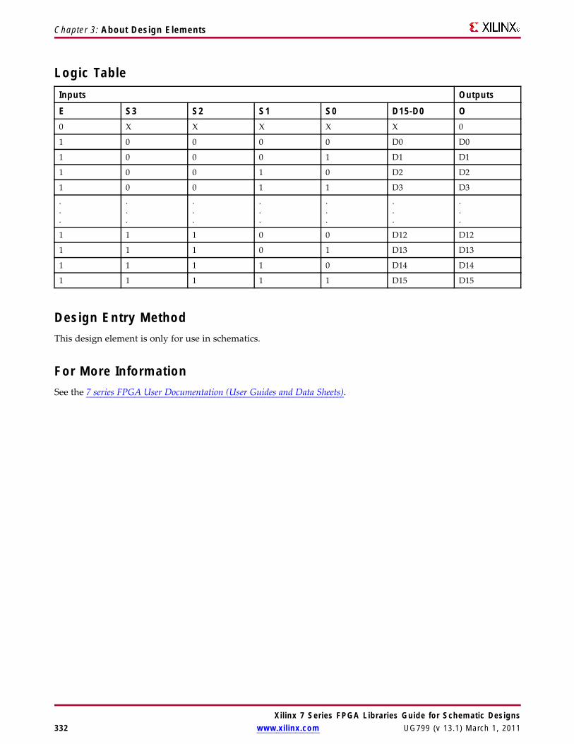
Chapter 3: About Design Elements
Logic TableInputs Outputs
E S3 S2 S1 S0 D15-D0 O0 X X X X X 0
1 0 0 0 0 D0 D0
1 0 0 0 1 D1 D1
1 0 0 1 0 D2 D2
1 0 0 1 1 D3 D3...
.
.
.
.
.
.
.
.
.
.
.
.
.
.
.
.
.
.
1 1 1 0 0 D12 D12
1 1 1 0 1 D13 D13
1 1 1 1 0 D14 D14
1 1 1 1 1 D15 D15
Design Entry MethodThis design element is only for use in schematics.
For More InformationSee the 7 series FPGA User Documentation (User Guides and Data Sheets).
Xilinx 7 Series FPGA Libraries Guide for Schematic Designs332 www.xilinx.com UG799 (v 13.1) March 1, 2011

Chapter 3: About Design Elements
M2_1Macro: 2-to-1 Multiplexer
IntroductionThis design element chooses one data bit from two sources (D1 or D0) under the control of the select input (S0).The output (O) reflects the state of the selected data input. When Low, S0 selects D0 and when High, S0 selects D1.
Logic TableInputs Outputs
S0 D1 D0 O1 D1 X D1
0 X D0 D0
Design Entry MethodThis design element is only for use in schematics.
For More InformationSee the 7 series FPGA User Documentation (User Guides and Data Sheets).
Xilinx 7 Series FPGA Libraries Guide for Schematic DesignsUG799 (v 13.1) March 1, 2011 www.xilinx.com 333

Chapter 3: About Design Elements
M2_1B1Macro: 2-to-1 Multiplexer with D0 Inverted
IntroductionThis design element chooses one data bit from two sources (D1 or D0) under the control of select input (S0).When S0 is Low, the output (O) reflects the inverted value of (D0). When S0 is High, (O) reflects the state of D1.
Logic TableInputs Outputs
S0 D1 D0 O1 1 X 1
1 0 X 0
0 X 1 0
0 X 0 1
Design Entry MethodThis design element is only for use in schematics.
For More InformationSee the 7 series FPGA User Documentation (User Guides and Data Sheets).
Xilinx 7 Series FPGA Libraries Guide for Schematic Designs334 www.xilinx.com UG799 (v 13.1) March 1, 2011
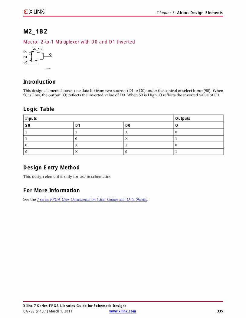
Chapter 3: About Design Elements
M2_1B2Macro: 2-to-1 Multiplexer with D0 and D1 Inverted
IntroductionThis design element chooses one data bit from two sources (D1 or D0) under the control of select input (S0). WhenS0 is Low, the output (O) reflects the inverted value of D0. When S0 is High, O reflects the inverted value of D1.
Logic TableInputs Outputs
S0 D1 D0 O1 1 X 0
1 0 X 1
0 X 1 0
0 X 0 1
Design Entry MethodThis design element is only for use in schematics.
For More InformationSee the 7 series FPGA User Documentation (User Guides and Data Sheets).
Xilinx 7 Series FPGA Libraries Guide for Schematic DesignsUG799 (v 13.1) March 1, 2011 www.xilinx.com 335

Chapter 3: About Design Elements
M2_1EMacro: 2-to-1 Multiplexer with Enable
IntroductionThis design element is a 2-to-1 multiplexer with enable. When the enable input (E) is High, the M2_1E choosesone data bit from two sources (D1 or D0) under the control of select input (S0). When Low, S0 selects D0 andwhen High, S0 selects D1. When (E) is Low, the output is Low.
Logic TableInputs Outputs
E S0 D1 D0 O0 X X X 0
1 0 X 1 1
1 0 X 0 0
1 1 1 X 1
1 1 0 X 0
Design Entry MethodThis design element is only for use in schematics.
For More InformationSee the 7 series FPGA User Documentation (User Guides and Data Sheets).
Xilinx 7 Series FPGA Libraries Guide for Schematic Designs336 www.xilinx.com UG799 (v 13.1) March 1, 2011

Chapter 3: About Design Elements
M4_1EMacro: 4-to-1 Multiplexer with Enable
IntroductionThis design element is a 4-to-1 multiplexer with enable. When the enable input (E) is High, the M4_1Emultiplexerchooses one data bit from four sources (D3, D2, D1, or D0) under the control of the select inputs (S1 : S0). Theoutput (O) reflects the state of the selected input as shown in the logic table. When (E) is Low, the output is Low.
Logic TableInputs Outputs
E S1 S0 D0 D1 D2 D3 O0 X X X X X X 0
1 0 0 D0 X X X D0
1 0 1 X D1 X X D1
1 1 0 X X D2 X D2
1 1 1 X X X D3 D3
Design Entry MethodThis design element is only for use in schematics.
For More InformationSee the 7 series FPGA User Documentation (User Guides and Data Sheets).
Xilinx 7 Series FPGA Libraries Guide for Schematic DesignsUG799 (v 13.1) March 1, 2011 www.xilinx.com 337

Chapter 3: About Design Elements
M8_1EMacro: 8-to-1 Multiplexer with Enable
IntroductionThis design element is an 8-to-1 multiplexer with enable. When the enable input (E) is High, the M8_1Emultiplexer chooses one data bit from eight sources (D7 : D0) under the control of the select inputs (S2 : S0). Theoutput (O) reflects the state of the selected input as shown in the logic table. When (E) is Low, the output is Low.
Logic TableInputs Outputs
E S2 S1 S0 D7-D0 O0 X X X X 0
1 0 0 0 D0 D0
1 0 0 1 D1 D1
1 0 1 0 D2 D2
1 0 1 1 D3 D3
1 1 0 0 D4 D4
1 1 0 1 D5 D5
1 1 1 0 D6 D6
1 1 1 1 D7 D7
Design Entry MethodThis design element is only for use in schematics.
For More InformationSee the 7 series FPGA User Documentation (User Guides and Data Sheets).
Xilinx 7 Series FPGA Libraries Guide for Schematic Designs338 www.xilinx.com UG799 (v 13.1) March 1, 2011

Chapter 3: About Design Elements
MMCME2_ADVPrimitive: Advanced Mixed Mode Clock Manager
IntroductionThe MMCME2 is a mixed signal block designed to support frequency synthesis, clock network deskew, and jitterreduction. The clock outputs can each have an individual divide, phase shift and duty cycle based on the sameVCO frequency. Additionally, the MMCME2 supports dynamic phase shifting and fractional divides.
Port DescriptionsPort Type Width FunctionCLKFBIN Input 1 Feedback clock pin to the MMCM
CLKFBOUT Output 1 Dedicated MMCM Feedback clock output
CLKFBOUTB Output 1 Inverted CLKFBOUT
CLKFBSTOPPED Output 1 Status pin indicating that the feedback clock has stopped.
CLKINSEL Input 1 Signal controls the state of the input MUX, High = CLKIN1, Low =CLKIN2.
CLKINSTOPPED Output 1 Status pin indicating that the input clock has stopped.
CLKIN1 Input 1 Primary clock input.
CLKIN2 Input 1 Secondary clock input to dynamically switch the MMCM referenceclock.
CLKOUT0 Output 1 CLKOUT0 output
CLKOUT0B Output 1 Inverted CLKOUT0 output
CLKOUT1 Output 1 CLKOUT1 output
Xilinx 7 Series FPGA Libraries Guide for Schematic DesignsUG799 (v 13.1) March 1, 2011 www.xilinx.com 339

Chapter 3: About Design Elements
Port Type Width FunctionCLKOUT1B Output 1 Inverted CLKOUT1 output
CLKOUT2 Output 1 CLKOUT2 output
CLKOUT2B Output 1 Inverted CLKOUT2 output
CLKOUT3 Output 1 CLKOUT3 output
CLKOUT3B Output 1 Inverted CLKOUT3 output
CLKOUT4 Output 1 CLKOUT4 output
CLKOUT5 Output 1 CLKOUT5 output
CLKOUT6 Output 1 CLKOUT6 output
DADDR<6:0> Input 7 The dynamic reconfiguration address (DADDR) input bus provides areconfiguration address for the dynamic reconfiguration. When notused, all bits must be assigned zeros.
DCLK Input 1 The DCLK signal is the reference clock for the dynamic reconfigurationport.
DEN Input 1 The dynamic reconfiguration enable (DEN) provides the enablecontrol signal to access the dynamic reconfiguration feature. When thedynamic reconfiguration feature is not used, DEN must be tied Low.
DI<15:0> Input 16 The dynamic reconfiguration data input (DI) bus providesreconfiguration data. When not used, all bits must be set to zero.
DO<15:0> Output 16 The dynamic reconfiguration output bus provides MMCM data outputwhen using dynamic reconfiguration.
DRDY Output 1 The dynamic reconfiguration ready output (DRDY) provides theresponse to the DEN signal for the MMCMs dynamic reconfigurationfeature.
DWE Input 1 The dynamic reconfiguration write enable (DWE) input pin providesthe write enable control signal to write the DI data into the DADDRaddress. When not used, it must be tied Low.
LOCKED Output 1 An output from the MMCM that indicates when the MMCM hasachieved phase alignment within a predefined window and frequencymatching within a predefined PPM range. The MMCM automaticallylocks after power on, no extra reset is required. LOCKED will bedeasserted if the input clock stops or the phase alignment is violated(e.g., input clock phase shift). The MMCM automatically reacquireslock after LOCKED is deasserted.
PSCLK Input 1 Phase shift clock.
PSDONE Output 1 Phase shift done.
PSEN Input 1 Phase shift enable
PSINCDEC Input 1 Phase shift increment/decrement control.
PWRDWN Input 1 Powers down instantiated but unused MMCMs.
RST Input 1 Asynchronous reset signal. The RST signal is an asynchronous resetfor the MMCM. The MMCM will synchronously re-enable itself whenthis signal is released (i.e., MMCM re-enabled). A reset is not requiredwhen the input clock conditions change (e.g., frequency).
Design Entry MethodThis design element can be used in schematics.
Xilinx 7 Series FPGA Libraries Guide for Schematic Designs340 www.xilinx.com UG799 (v 13.1) March 1, 2011

Chapter 3: About Design Elements
Available AttributesAttribute Type Allowed Values Default DescriptionBANDWIDTH STRING OPTIMIZED, HIGH,
LOWOPTIMIZED Specifies the MMCM programming
algorithm affecting the jitter, phasemargin and other characteristics of theMMCM.
CLKFBOUT_MULT_F
3 significantdigit FLOAT
2.000 to 64.000 5.000 Specifies the amount to multiplyall CLKOUT clock outputs if adifferent frequency is desired. Thisnumber, in combination with theassociated CLKOUT#_DIVIDE valueand DIVCLK_DIVIDE value, willdetermine the output frequency. Eventhough this value needs to be specifiedas a real number only whole intergervalues are supported (i.e. 6.0 is OK but6.5 is not).
CLKFBOUT_PHASE
3 significantdigit FLOAT
-360.000 to 360.000 0.000 Specifies the phase offset in degreesof the clock feedback output. Shiftingthe feedback clock results in a negativephase shift of all output clocks to theMMCM.
CLKIN_PERIOD FLOAT(nS) 0.938 to 100.000 0.000 Specifies the input period in ns to theMMCM CLKIN inputs. Resolutionis down to the ps. For exmaple avalue of 33.333 would indicate a 33MHz input clock. This informationis mandatory and must be supplied.CLKIN1_PERIOD relates to the inputperiod on the CLKIN1 input whileCLKIN2_PERIOD relates to the inputclock period on the CLKIN2 input.
CLKOUT0_DIVIDE_F
3 significantdigit FLOAT
1.000 to 128.000 1.000 Specifies the amount to dividethe associated CLKOUT clockoutput if a different frequency isdesired. This number in combinationwith the CLKFBOUT_MULT andDIVCLK_DIVIDE values willdetermine the output frequency.
CLKOUT0_DIVIDE -CLKOUT6_DIVIDE
DECIMAL 1 to 128 1 Specifies the amount to dividethe associated CLKOUT clockoutput if a different frequency isdesired. This number in combinationwith the CLKFBOUT_MULT andDIVCLK_DIVIDE values willdetermine the output frequency.
CLKOUT0_DUTY_CYCLE -CLKOUT6_DUTY_CYCLE
3 significantdigit FLOAT
0.001 to 0.999 0.500 Specifies the Duty Cycle of theassociated CLKOUT clock output inpercentage (i.e., 0.50 will generate a50% duty cycle).
CLKOUT0_PHASE-CLKOUT6_PHASE
3 significantdigit FLOAT
-360.000 to 360.000 0.000 Specifies the phase offset in degreesof the clock feedback output. Shiftingthe feedback clock results in a negativephase shift of all output clocks to theMMCM.
Xilinx 7 Series FPGA Libraries Guide for Schematic DesignsUG799 (v 13.1) March 1, 2011 www.xilinx.com 341

Chapter 3: About Design Elements
Attribute Type Allowed Values Default DescriptionCLKOUT4_CASCADE
STRING FALSE, TRUE FALSE Cascades the output divider (counter)into the input of the CLKOUT4 dividerfor an output clock divider that isgreater than 128.
COMPENSATION STRING ZHOLD, BUF_IN,EXTERNAL,INTERNAL
ZHOLD Clock input compensation. Mustbe set to ZHOLD. Defines how theMMCM feedback is configured.ZHOLD indicates the MMCM isconfigured to provide a negative holdtime at the I/O registers. INTERNALindicates the MMCM is using its owninternal feedback path so no delayis being compensated. EXTERNALindicates a network external tothe FPGA is being compensated.CASCADE indicates cascading of 2MMCM BUF_IN indicates that theconfiguration does not match with theother compensation modes and nodelay will be compensated. This isthe case if a clock input is driven by aBUFG/BUFH/BUFR/GT.
DIVCLK_DIVIDE DECIMAL 1 to 106 1 Specifies the division ratio for alloutput clocks with respect to the inputclock. Effectively divides the CLKINgoing into the PFD.
REF_JITTER 3 significantdigit FLOAT
0.000 to 0.999 0.010 Allows specification of the expectedjitter on the CLKIN inputs in order tobetter optimize MMCM performance.A bandwidth setting of OPTIMIZEDwill attempt to choose the bestparameter for input clocking whenunknown. If known, then the valueprovided should be specified in termsof the UI percentage (the maximumpeak to peak value) of the expectedjitter on the input clock. REF_JITTER1relates to the input jitter on CLKIN1while REF_JITTER2 relates to the inputjitter on CLKIN2.
STARTUP_WAIT STRING FALSE, TRUE FALSE Not supported. Must be set to FALSE.
USE_FINE_PS STRING FALSE, TRUE FALSE Counter variable fine phase shiftenable.
For More InformationSee the 7 series FPGA User Documentation (User Guides and Data Sheets).
Xilinx 7 Series FPGA Libraries Guide for Schematic Designs342 www.xilinx.com UG799 (v 13.1) March 1, 2011

Chapter 3: About Design Elements
MMCME2_BASEPrimitive: Mixed signal block designed to support clock network deskew, frequencysynthesis, and jitter reduction.
IntroductionThis component is a mixed signal block designed to support clock network deskew, frequency synthesis,and jitter reduction. The seven "O" counters can be independently programmed which means O0 could beprogrammed to do a divide by 2 while O1 is programmed to do a divide by 3. The only constraint is that theVCO operating frequency must be the same for all the output counters since a single VCO drives all the counters.The CLKFBOUT and CLKFBOUTB pins can be used to drive logic but it must be equal to the CLKin frequency.
Port DescriptionsPort Type Width FunctionCLKFBIN Input 1 Feedback clock input.
CLKFBOUT Output 1 Dedicated MMCM feedback output.
CLKFBOUTB Output 1 Inverted MMCM feedback clock output.
CLKIN1 Input 1 General clock input.
CLKOUT[0:6] Output 7, 1-bit User configurable clock outputs (0 through 6) that can be dividedversions of the VCO phase outputs (user controllable) from 1(bypassed) to 128. The output clocks are phase aligned to eachother (unless phase shifted) and aligned to the input clock with aproper feedback configuration.
CLKOUT[0:3]B Output 4, 1-bit Inverted CLKOUT[0:3].
Xilinx 7 Series FPGA Libraries Guide for Schematic DesignsUG799 (v 13.1) March 1, 2011 www.xilinx.com 343

Chapter 3: About Design Elements
Port Type Width FunctionLOCKED Output 1 An output from the MMCM that indicates when the MMCM
has achieved phase alignment within a predefined window andfrequency matching within a predefined PPM range. The MMCMautomatically locks after power on. No extra reset is required.LOCKED will be deasserted if the input clock stops or the phasealignment is violated (e.g., input clock phase shift). The MMCMautomatically reacquires lock after LOCKED is deasserted.
PWRDWN Input 1 Powers down instantiated but unused MMCMs.
RST Input 1 Asynchronous reset signal. The RST signal is an asynchronousreset for the MMCM. The MMCM will synchronously re-enableitself when this signal is released (i.e., MMCM re-enabled). Areset is not required when the input clock conditions change (e.g.,frequency).
Design Entry MethodThis design element can be used in schematics.
Available Attributes
Attribute TypeAllowedValues Default Description
BANDWIDTH String “OPTIMIZED”,“HIGH”,“LOW”
“OPTIMIZED” Specifies the MMCM programmingalgorithm affecting the jitter, phase margin,and other characteristics of the MMCM.
CLKFBOUT_MULT_F 3 significantdigit Float
5.0 to64.0
1.0 Specifies the amount to multiplyall CLKOUT clock outputs if adifferent frequency is desired. Thisnumber, in combination with theassociated CLKOUT#_DIVIDE value andDIVCLK_DIVIDE value, will determine theoutput frequency.
CLKFBOUT_PHASE 3 significantdigit Float
-360.000 to360.000
0.000 Specifies the phase offset in degrees ofthe clock feedback output. Shifting thefeedback clock results in a negative phaseshift of all output clocks to the MMCM.
CLKIN1_PERIOD Float (nS) 1.000 to1000.000
0.000 Specifies the input period in ns to theMMCM CLKIN1 input. Resolution is downto the ps. This information is mandatoryand must be supplied.
CLKOUT0_DIVIDE_F 3 significantdigit Float
1.000 to128.000
1.000 Specifies the amount to divide theassociated CLKOUT clock output if adifferent frequency is desired. This numberin combination with the CLKFBOUT_MULTandDIVCLK_DIVIDE valueswill determinethe output frequency.
CLKOUT[0:6]_DUTY_CYCLE
3 significantdigit Float
0.001 to0.999
0.500 Specifies the Duty Cycle of the associatedCLKOUT clock output in percentage (i.e.,0.50 will generate a 50% duty cycle).
Xilinx 7 Series FPGA Libraries Guide for Schematic Designs344 www.xilinx.com UG799 (v 13.1) March 1, 2011

Chapter 3: About Design Elements
Attribute TypeAllowedValues Default Description
CLKOUT[0:6]_PHASE 3 significantdigit Float
-360.000 to360.000
0.000 Allows specification of the output phaserelationship of the associated CLKOUTclock output in number of degrees offset(i.e., 90 indicates a 90° or ¼ cycle offsetphase offset while 180 indicates a 180° offsetor ½ cycle phase offset).
CLOCK_HOLD Boolean FALSE, TRUE FALSE When TRUE, holds the VCO frequency closeto the frequency prior to losing CLKIN.
DIVCLK_DIVIDE Integer 1 to 128 1 Specifies the division ratio for all outputclocks with respect to the input clock.Effectively divides the CLKIN going intothe PFD.
REF_JITTER1 3 significantdigit Float
0.000 to0.999
0.010 Allows specification of the expectedjitter on the reference clock in order tobetter optimize MMCM performance. Abandwidth setting of OPTIMIZED willattempt to choose the best parameter forinput clocking when unknown. If known,then the value provided should be specifiedin terms of the UI percentage (the maximumpeak to peak value) of the expected jitter onthe input clock.
STARTUP_WAIT Boolean FALSE FALSE This attribute is not supported.
For More InformationSee the 7 series FPGA User Documentation (User Guides and Data Sheets).
Xilinx 7 Series FPGA Libraries Guide for Schematic DesignsUG799 (v 13.1) March 1, 2011 www.xilinx.com 345

Chapter 3: About Design Elements
MULT18X18Primitive: 18 x 18 Signed Multiplier
IntroductionMULT18X18 is a combinational signed 18-bit by 18-bit multiplier. The value represented in the 18-bit input A ismultiplied by the value represented in the 18-bit input B. Output P is the 36-bit product of A and B.
Logic TableInputs OutputA B PA B A x B
A, B, and P are two’s complement.
Design Entry MethodThis design element can be used in schematics.
For More InformationSee the 7 series FPGA User Documentation (User Guides and Data Sheets).
Xilinx 7 Series FPGA Libraries Guide for Schematic Designs346 www.xilinx.com UG799 (v 13.1) March 1, 2011

Chapter 3: About Design Elements
MULT18X18SPrimitive: 18 x 18 Signed Multiplier Registered Version
IntroductionMULT18X18S is the registered version of the 18 x 18 signed multiplier with output P and inputs A, B, C, CE, andR. The registers are initialized to 0 after the GSR pulse.
The value represented in the 18-bit input A is multiplied by the value represented in the 18-bit input B. Output Pis the 36-bit product of A and B.
Logic TableInputs Output
C CE Am Bn R P
↑ X X X 1 0
↑ 1 Am Bn 0 A x B
X 0 X X 0 No Change
A, B, and P are two’s complement.
Design Entry MethodThis design element can be used in schematics.
For More InformationSee the 7 series FPGA User Documentation (User Guides and Data Sheets).
Xilinx 7 Series FPGA Libraries Guide for Schematic DesignsUG799 (v 13.1) March 1, 2011 www.xilinx.com 347

Chapter 3: About Design Elements
MUXCYPrimitive: 2-to-1 Multiplexer for Carry Logic with General Output
IntroductionThe direct input (DI) of a slice is connected to the (DI) input of the MUXCY. The carry in (CI) input of an LCis connected to the CI input of the MUXCY. The select input (S) of the MUXCY is driven by the output of thelook-up table (LUT) and configured as a MUX function. The carry out (O) of the MUXCY reflects the state of theselected input and implements the carry out function of each LC. When Low, S selects DI; when High, S selects CI.
The variants “MUXCY_D” and “MUXCY_L” provide additional types of outputs that can be used by differenttiming models for more accurate pre-layout timing estimation.
Logic TableInputs Outputs
S DI CI O0 1 X 1
0 0 X 0
1 X 1 1
1 X 0 0
Design Entry MethodThis design element can be used in schematics.
For More InformationSee the 7 series FPGA User Documentation (User Guides and Data Sheets).
Xilinx 7 Series FPGA Libraries Guide for Schematic Designs348 www.xilinx.com UG799 (v 13.1) March 1, 2011

Chapter 3: About Design Elements
MUXCY_DPrimitive: 2-to-1 Multiplexer for Carry Logic with Dual Output
IntroductionThis design element implements a 1-bit, high-speed carry propagate function. One such function can beimplemented per logic cell (LC), for a total of 4-bits per configurable logic block (CLB). The direct input (DI) ofan LC is connected to the DI input of the MUXCY_D. The carry in (CI) input of an LC is connected to the CIinput of the MUXCY_D. The select input (S) of the MUX is driven by the output of the look-up table (LUT) andconfigured as an XOR function. The carry out (O and LO) of the MUXCY_D reflects the state of the selected inputand implements the carry out function of each LC. When Low, S selects DI; when High, S selects CI.
Outputs O and LO are functionally identical. The O output is a general interconnect. See also “MUXCY”and “MUXCY_L”.
Logic TableInputs Outputs
S DI CI O LO0 1 X 1 1
0 0 X 0 0
1 X 1 1 1
1 X 0 0 0
Design Entry MethodThis design element can be used in schematics.
For More InformationSee the 7 series FPGA User Documentation (User Guides and Data Sheets).
Xilinx 7 Series FPGA Libraries Guide for Schematic DesignsUG799 (v 13.1) March 1, 2011 www.xilinx.com 349

Chapter 3: About Design Elements
MUXCY_LPrimitive: 2-to-1 Multiplexer for Carry Logic with Local Output
IntroductionThis design element implements a 1-bit high-speed carry propagate function. One such function is implementedper logic cell (LC), for a total of 4-bits per configurable logic block (CLB). The direct input (DI) of an LC isconnected to the DI input of the MUXCY_L. The carry in (CI) input of an LC is connected to the CI input ofthe MUXCY_L. The select input (S) of the MUXCY_L is driven by the output of the look-up table (LUT) andconfigured as an XOR function. The carry out (LO) of the MUXCY_L reflects the state of the selected input andimplements the carry out function of each (LC). When Low, (S) selects DI; when High, (S) selects (CI).
See also “MUXCY” and “MUXCY_D.”
Logic TableInputs Outputs
S DI CI LO0 1 X 1
0 0 X 0
1 X 1 1
1 X 0 0
Design Entry MethodThis design element can be used in schematics.
For More InformationSee the 7 series FPGA User Documentation (User Guides and Data Sheets).
Xilinx 7 Series FPGA Libraries Guide for Schematic Designs350 www.xilinx.com UG799 (v 13.1) March 1, 2011

Chapter 3: About Design Elements
MUXF7Primitive: 2-to-1 Look-Up Table Multiplexer with General Output
IntroductionThis design element provides a multiplexer function for use in creating a function-of-7 look-up table or an 8-to-1multiplexer in combination with the associated look-up tables. Local outputs (LO) of MUXF6 are connectedto the I0 and I1 inputs of the MUXF7. The S input is driven from any internal net. When Low, S selects I0.When High, S selects I1.
The variants, “MUXF7_D” and “MUXF7_L”, provide additional types of outputs that can be used by differenttiming models for more accurate pre-layout timing estimation.
Logic TableInputs Outputs
S I0 I1 O0 I0 X I0
1 X I1 I1
X 0 0 0
X 1 1 1
Port DescriptionsPort Direction Width FunctionO Output 1 Output of MUX to general routing.
I0 Input 1 Input (tie to MUXF6 LO out).
I1 Input 1 Input (tie to MUXF6 LO out).
S Input 1 Input select to MUX.
Design Entry MethodThis design element can be used in schematics.
For More InformationSee the 7 series FPGA User Documentation (User Guides and Data Sheets).
Xilinx 7 Series FPGA Libraries Guide for Schematic DesignsUG799 (v 13.1) March 1, 2011 www.xilinx.com 351

Chapter 3: About Design Elements
MUXF7_DPrimitive: 2-to-1 Look-Up Table Multiplexer with Dual Output
IntroductionThis design element provides a multiplexer function for use in creating a function-of-7 look-up table or a 16-to-1multiplexer in combination with the associated look-up tables. Local outputs (LO) of MUXF6 are connectedto the I0 and I1 inputs of the MUXF7. The S input is driven from any internal net. When Low, S selects I0.When High, S selects I1.
Outputs O and LO are functionally identical. The O output is a general interconnect. The LO output connects toother inputs in the same CLB slice.
Logic TableInputs Outputs
S I0 I1 O LO0 I0 X I0 I0
1 X I1 I1 I1
X 0 0 0 0
X 1 1 1 1
Port DescriptionsPort Direction Width FunctionO Output 1 Output of MUX to general routing.
LO Output 1 Output of MUX to local routing.
I0 Input 1 Input (tie to MUXF6 LO out).
I1 Input 1 Input (tie to MUXF6 LO out).
S Input 1 Input select to MUX.
Design Entry MethodThis design element can be used in schematics.
For More InformationSee the 7 series FPGA User Documentation (User Guides and Data Sheets).
Xilinx 7 Series FPGA Libraries Guide for Schematic Designs352 www.xilinx.com UG799 (v 13.1) March 1, 2011

Chapter 3: About Design Elements
MUXF7_LPrimitive: 2-to-1 look-up table Multiplexer with Local Output
IntroductionThis design element provides a multiplexer function for use in creating a function-of-7 look-up table or a 16-to-1multiplexer in combination with the associated look-up tables. Local outputs (LO) of MUXF6 are connectedto the I0 and I1 inputs of the MUXF7. The S input is driven from any internal net. When Low, S selects I0.When High, S selects I1.
The LO output connects to other inputs in the same CLB slice.
Logic TableInputs Output
S I0 I1 LO0 I0 X I0
1 X I1 I1
X 0 0 0
X 1 1 1
Port DescriptionsPort Direction Width FunctionLO Output 1 Output of MUX to local routing
I0 Input 1 Input
I1 Input 1 Input
S Input 1 Input select to MUX
Design Entry MethodThis design element can be used in schematics.
For More InformationSee the 7 series FPGA User Documentation (User Guides and Data Sheets).
Xilinx 7 Series FPGA Libraries Guide for Schematic DesignsUG799 (v 13.1) March 1, 2011 www.xilinx.com 353

Chapter 3: About Design Elements
MUXF8Primitive: 2-to-1 Look-Up Table Multiplexer with General Output
IntroductionThis design element provides a multiplexer function in eight slices for creating a function-of-8 look-up table or a16-to-1 multiplexer in combination with the associated look-up tables, MUXF5s, MUXF6s, and MUXF7s. Localoutputs (LO) of MUXF7 are connected to the I0 and I1 inputs of the MUXF8. The S input is driven from anyinternal net. When Low, S selects I0. When High, S selects I1.
Logic TableInputs Outputs
S I0 I1 O0 I0 X I0
1 X I1 I1
X 0 0 0
X 1 1 1
Port DescriptionsPort Direction Width FunctionO Output 1 Output of MUX to general routing
I0 Input 1 Input (tie to MUXF7 LO out)
I1 Input 1 Input (tie to MUXF7 LO out)
S Input 1 Input select to MUX
Design Entry MethodThis design element can be used in schematics.
For More InformationSee the 7 series FPGA User Documentation (User Guides and Data Sheets).
Xilinx 7 Series FPGA Libraries Guide for Schematic Designs354 www.xilinx.com UG799 (v 13.1) March 1, 2011

Chapter 3: About Design Elements
MUXF8_DPrimitive: 2-to-1 Look-Up Table Multiplexer with Dual Output
IntroductionThis design element provides a multiplexer function in eight slices for creating a function-of-8 look-up table or a32-to-1 multiplexer in combination with the associated four look-up tables and two MUXF8s. Local outputs(LO) of MUXF7 are connected to the I0 and I1 inputs of the MUXF8. The S input is driven from any internalnet. When Low, S selects I0. When High, S selects I1.
Outputs O and LO are functionally identical. The O output is a general interconnect. The LO output connects toother inputs in the same CLB slice.
Logic TableInputs Outputs
S I0 I1 O LO0 I0 X I0 I0
1 X I1 I1 I1
X 0 0 0 0
X 1 1 1 1
Port DescriptionsPort Direction Width FunctionO Output 1 Output of MUX to general routing
LO Output 1 Output of MUX to local routing
I0 Input 1 Input (tie to MUXF7 LO out)
I1 Input 1 Input (tie to MUXF7 LO out)
S Input 1 Input select to MUX
Design Entry MethodThis design element can be used in schematics.
For More InformationSee the 7 series FPGA User Documentation (User Guides and Data Sheets).
Xilinx 7 Series FPGA Libraries Guide for Schematic DesignsUG799 (v 13.1) March 1, 2011 www.xilinx.com 355

Chapter 3: About Design Elements
MUXF8_LPrimitive: 2-to-1 Look-Up Table Multiplexer with Local Output
IntroductionThis design element provides a multiplexer function in eight slices for creating a function-of-8 look-up table or a32-to-1 multiplexer in combination with the associated four look-up tables and two MUXF8s. Local outputs(LO) of MUXF7 are connected to the I0 and I1 inputs of the MUXF8. The S input is driven from any internalnet. When Low, S selects I0. When High, S selects I1.
The LO output connects to other inputs in the same CLB slice.
Logic TableInputs Output
S I0 I1 LO0 I0 X I0
1 X I1 I1
X 0 0 0
X 1 1 1
Port DescriptionsPort Direction Width FunctionLO Output 1 Output of MUX to local routing
I0 Input 1 Input (tie to MUXF7 LO out)
I1 Input 1 Input (tie to MUXF7 LO out)
S Input 1 Input select to MUX
Design Entry MethodThis design element can be used in schematics.
For More InformationSee the 7 series FPGA User Documentation (User Guides and Data Sheets).
Xilinx 7 Series FPGA Libraries Guide for Schematic Designs356 www.xilinx.com UG799 (v 13.1) March 1, 2011

Chapter 3: About Design Elements
NAND12Macro: 12- Input NAND Gate with Non-Inverted Inputs
IntroductionNAND gates of up to five inputs are available in any combination of inverting and non-inverting inputs. NANDgates of six to nine inputs, 12 inputs, and 16 inputs are available with only non-inverting inputs. To invert inputs,use external inverters. Because each input uses a CLB resource, replace gates with unused inputs with gateshaving the necessary number of inputs.
Design Entry MethodThis design element is only for use in schematics.
For More InformationSee the 7 series FPGA User Documentation (User Guides and Data Sheets).
Xilinx 7 Series FPGA Libraries Guide for Schematic DesignsUG799 (v 13.1) March 1, 2011 www.xilinx.com 357
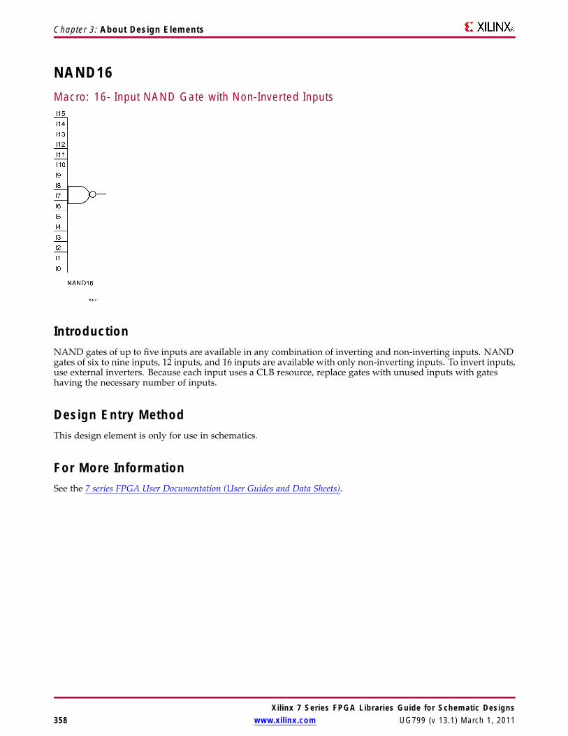
Chapter 3: About Design Elements
NAND16Macro: 16- Input NAND Gate with Non-Inverted Inputs
IntroductionNAND gates of up to five inputs are available in any combination of inverting and non-inverting inputs. NANDgates of six to nine inputs, 12 inputs, and 16 inputs are available with only non-inverting inputs. To invert inputs,use external inverters. Because each input uses a CLB resource, replace gates with unused inputs with gateshaving the necessary number of inputs.
Design Entry MethodThis design element is only for use in schematics.
For More InformationSee the 7 series FPGA User Documentation (User Guides and Data Sheets).
Xilinx 7 Series FPGA Libraries Guide for Schematic Designs358 www.xilinx.com UG799 (v 13.1) March 1, 2011

Chapter 3: About Design Elements
NAND2Primitive: 2-Input NAND Gate with Non-Inverted Inputs
IntroductionNAND gates of up to five inputs are available in any combination of inverting and non-inverting inputs. NANDgates of six to nine inputs, 12 inputs, and 16 inputs are available with only non-inverting inputs. To invert inputs,use external inverters. Because each input uses a CLB resource, replace gates with unused inputs with gateshaving the necessary number of inputs.
Design Entry MethodThis design element is only for use in schematics.
For More InformationSee the 7 series FPGA User Documentation (User Guides and Data Sheets).
Xilinx 7 Series FPGA Libraries Guide for Schematic DesignsUG799 (v 13.1) March 1, 2011 www.xilinx.com 359

Chapter 3: About Design Elements
NAND2B1Primitive: 2-Input NAND Gate with 1 Inverted and 1 Non-Inverted Inputs
IntroductionNAND gates of up to five inputs are available in any combination of inverting and non-inverting inputs. NANDgates of six to nine inputs, 12 inputs, and 16 inputs are available with only non-inverting inputs. To invert inputs,use external inverters. Because each input uses a CLB resource, replace gates with unused inputs with gateshaving the necessary number of inputs.
Design Entry MethodThis design element is only for use in schematics.
For More InformationSee the 7 series FPGA User Documentation (User Guides and Data Sheets).
Xilinx 7 Series FPGA Libraries Guide for Schematic Designs360 www.xilinx.com UG799 (v 13.1) March 1, 2011
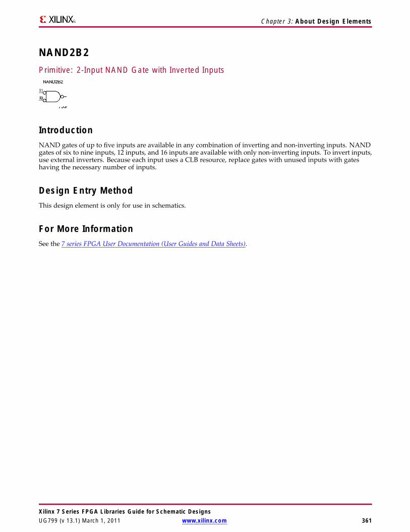
Chapter 3: About Design Elements
NAND2B2Primitive: 2-Input NAND Gate with Inverted Inputs
IntroductionNAND gates of up to five inputs are available in any combination of inverting and non-inverting inputs. NANDgates of six to nine inputs, 12 inputs, and 16 inputs are available with only non-inverting inputs. To invert inputs,use external inverters. Because each input uses a CLB resource, replace gates with unused inputs with gateshaving the necessary number of inputs.
Design Entry MethodThis design element is only for use in schematics.
For More InformationSee the 7 series FPGA User Documentation (User Guides and Data Sheets).
Xilinx 7 Series FPGA Libraries Guide for Schematic DesignsUG799 (v 13.1) March 1, 2011 www.xilinx.com 361
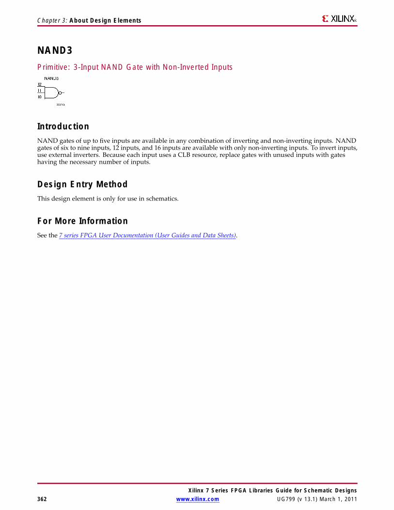
Chapter 3: About Design Elements
NAND3Primitive: 3-Input NAND Gate with Non-Inverted Inputs
IntroductionNAND gates of up to five inputs are available in any combination of inverting and non-inverting inputs. NANDgates of six to nine inputs, 12 inputs, and 16 inputs are available with only non-inverting inputs. To invert inputs,use external inverters. Because each input uses a CLB resource, replace gates with unused inputs with gateshaving the necessary number of inputs.
Design Entry MethodThis design element is only for use in schematics.
For More InformationSee the 7 series FPGA User Documentation (User Guides and Data Sheets).
Xilinx 7 Series FPGA Libraries Guide for Schematic Designs362 www.xilinx.com UG799 (v 13.1) March 1, 2011

Chapter 3: About Design Elements
NAND3B1Primitive: 3-Input NAND Gate with 1 Inverted and 2 Non-Inverted Inputs
IntroductionNAND gates of up to five inputs are available in any combination of inverting and non-inverting inputs. NANDgates of six to nine inputs, 12 inputs, and 16 inputs are available with only non-inverting inputs. To invert inputs,use external inverters. Because each input uses a CLB resource, replace gates with unused inputs with gateshaving the necessary number of inputs.
Design Entry MethodThis design element is only for use in schematics.
For More InformationSee the 7 series FPGA User Documentation (User Guides and Data Sheets).
Xilinx 7 Series FPGA Libraries Guide for Schematic DesignsUG799 (v 13.1) March 1, 2011 www.xilinx.com 363

Chapter 3: About Design Elements
NAND3B2Primitive: 3-Input NAND Gate with 2 Inverted and 1 Non-Inverted Inputs
IntroductionNAND gates of up to five inputs are available in any combination of inverting and non-inverting inputs. NANDgates of six to nine inputs, 12 inputs, and 16 inputs are available with only non-inverting inputs. To invert inputs,use external inverters. Because each input uses a CLB resource, replace gates with unused inputs with gateshaving the necessary number of inputs.
Design Entry MethodThis design element is only for use in schematics.
For More InformationSee the 7 series FPGA User Documentation (User Guides and Data Sheets).
Xilinx 7 Series FPGA Libraries Guide for Schematic Designs364 www.xilinx.com UG799 (v 13.1) March 1, 2011

Chapter 3: About Design Elements
NAND3B3Primitive: 3-Input NAND Gate with Inverted Inputs
IntroductionNAND gates of up to five inputs are available in any combination of inverting and non-inverting inputs. NANDgates of six to nine inputs, 12 inputs, and 16 inputs are available with only non-inverting inputs. To invert inputs,use external inverters. Because each input uses a CLB resource, replace gates with unused inputs with gateshaving the necessary number of inputs.
Design Entry MethodThis design element is only for use in schematics.
For More InformationSee the 7 series FPGA User Documentation (User Guides and Data Sheets).
Xilinx 7 Series FPGA Libraries Guide for Schematic DesignsUG799 (v 13.1) March 1, 2011 www.xilinx.com 365

Chapter 3: About Design Elements
NAND4Primitive: 4-Input NAND Gate with Non-Inverted Inputs
IntroductionNAND gates of up to five inputs are available in any combination of inverting and non-inverting inputs. NANDgates of six to nine inputs, 12 inputs, and 16 inputs are available with only non-inverting inputs. To invert inputs,use external inverters. Because each input uses a CLB resource, replace gates with unused inputs with gateshaving the necessary number of inputs.
Design Entry MethodThis design element is only for use in schematics.
For More InformationSee the 7 series FPGA User Documentation (User Guides and Data Sheets).
Xilinx 7 Series FPGA Libraries Guide for Schematic Designs366 www.xilinx.com UG799 (v 13.1) March 1, 2011

Chapter 3: About Design Elements
NAND4B1Primitive: 4-Input NAND Gate with 1 Inverted and 3 Non-Inverted Inputs
IntroductionNAND gates of up to five inputs are available in any combination of inverting and non-inverting inputs. NANDgates of six to nine inputs, 12 inputs, and 16 inputs are available with only non-inverting inputs. To invert inputs,use external inverters. Because each input uses a CLB resource, replace gates with unused inputs with gateshaving the necessary number of inputs.
Design Entry MethodThis design element is only for use in schematics.
For More InformationSee the 7 series FPGA User Documentation (User Guides and Data Sheets).
Xilinx 7 Series FPGA Libraries Guide for Schematic DesignsUG799 (v 13.1) March 1, 2011 www.xilinx.com 367

Chapter 3: About Design Elements
NAND4B2Primitive: 4-Input NAND Gate with 2 Inverted and 2 Non-Inverted Inputs
IntroductionNAND gates of up to five inputs are available in any combination of inverting and non-inverting inputs. NANDgates of six to nine inputs, 12 inputs, and 16 inputs are available with only non-inverting inputs. To invert inputs,use external inverters. Because each input uses a CLB resource, replace gates with unused inputs with gateshaving the necessary number of inputs.
Design Entry MethodThis design element is only for use in schematics.
For More InformationSee the 7 series FPGA User Documentation (User Guides and Data Sheets).
Xilinx 7 Series FPGA Libraries Guide for Schematic Designs368 www.xilinx.com UG799 (v 13.1) March 1, 2011

Chapter 3: About Design Elements
NAND4B3Primitive: 4-Input NAND Gate with 3 Inverted and 1 Non-Inverted Inputs
IntroductionNAND gates of up to five inputs are available in any combination of inverting and non-inverting inputs. NANDgates of six to nine inputs, 12 inputs, and 16 inputs are available with only non-inverting inputs. To invert inputs,use external inverters. Because each input uses a CLB resource, replace gates with unused inputs with gateshaving the necessary number of inputs.
Design Entry MethodThis design element is only for use in schematics.
For More InformationSee the 7 series FPGA User Documentation (User Guides and Data Sheets).
Xilinx 7 Series FPGA Libraries Guide for Schematic DesignsUG799 (v 13.1) March 1, 2011 www.xilinx.com 369

Chapter 3: About Design Elements
NAND4B4Primitive: 4-Input NAND Gate with Inverted Inputs
IntroductionNAND gates of up to five inputs are available in any combination of inverting and non-inverting inputs. NANDgates of six to nine inputs, 12 inputs, and 16 inputs are available with only non-inverting inputs. To invert inputs,use external inverters. Because each input uses a CLB resource, replace gates with unused inputs with gateshaving the necessary number of inputs.
Design Entry MethodThis design element is only for use in schematics.
For More InformationSee the 7 series FPGA User Documentation (User Guides and Data Sheets).
Xilinx 7 Series FPGA Libraries Guide for Schematic Designs370 www.xilinx.com UG799 (v 13.1) March 1, 2011

Chapter 3: About Design Elements
NAND5Primitive: 5-Input NAND Gate with Non-Inverted Inputs
IntroductionNAND gates of up to five inputs are available in any combination of inverting and non-inverting inputs. NANDgates of six to nine inputs, 12 inputs, and 16 inputs are available with only non-inverting inputs. To invert inputs,use external inverters. Because each input uses a CLB resource, replace gates with unused inputs with gateshaving the necessary number of inputs.
Design Entry MethodThis design element is only for use in schematics.
For More InformationSee the 7 series FPGA User Documentation (User Guides and Data Sheets).
Xilinx 7 Series FPGA Libraries Guide for Schematic DesignsUG799 (v 13.1) March 1, 2011 www.xilinx.com 371

Chapter 3: About Design Elements
NAND5B1Primitive: 5-Input NAND Gate with 1 Inverted and 4 Non-Inverted Inputs
IntroductionNAND gates of up to five inputs are available in any combination of inverting and non-inverting inputs. NANDgates of six to nine inputs, 12 inputs, and 16 inputs are available with only non-inverting inputs. To invert inputs,use external inverters. Because each input uses a CLB resource, replace gates with unused inputs with gateshaving the necessary number of inputs.
Design Entry MethodThis design element is only for use in schematics.
For More InformationSee the 7 series FPGA User Documentation (User Guides and Data Sheets).
Xilinx 7 Series FPGA Libraries Guide for Schematic Designs372 www.xilinx.com UG799 (v 13.1) March 1, 2011

Chapter 3: About Design Elements
NAND5B2Primitive: 5-Input NAND Gate with 2 Inverted and 3 Non-Inverted Inputs
IntroductionNAND gates of up to five inputs are available in any combination of inverting and non-inverting inputs. NANDgates of six to nine inputs, 12 inputs, and 16 inputs are available with only non-inverting inputs. To invert inputs,use external inverters. Because each input uses a CLB resource, replace gates with unused inputs with gateshaving the necessary number of inputs.
Design Entry MethodThis design element is only for use in schematics.
For More InformationSee the 7 series FPGA User Documentation (User Guides and Data Sheets).
Xilinx 7 Series FPGA Libraries Guide for Schematic DesignsUG799 (v 13.1) March 1, 2011 www.xilinx.com 373

Chapter 3: About Design Elements
NAND5B3Primitive: 5-Input NAND Gate with 3 Inverted and 2 Non-Inverted Inputs
IntroductionNAND gates of up to five inputs are available in any combination of inverting and non-inverting inputs. NANDgates of six to nine inputs, 12 inputs, and 16 inputs are available with only non-inverting inputs. To invert inputs,use external inverters. Because each input uses a CLB resource, replace gates with unused inputs with gateshaving the necessary number of inputs.
Design Entry MethodThis design element is only for use in schematics.
For More InformationSee the 7 series FPGA User Documentation (User Guides and Data Sheets).
Xilinx 7 Series FPGA Libraries Guide for Schematic Designs374 www.xilinx.com UG799 (v 13.1) March 1, 2011

Chapter 3: About Design Elements
NAND5B4Primitive: 5-Input NAND Gate with 4 Inverted and 1 Non-Inverted Inputs
IntroductionNAND gates of up to five inputs are available in any combination of inverting and non-inverting inputs. NANDgates of six to nine inputs, 12 inputs, and 16 inputs are available with only non-inverting inputs. To invert inputs,use external inverters. Because each input uses a CLB resource, replace gates with unused inputs with gateshaving the necessary number of inputs.
Design Entry MethodThis design element is only for use in schematics.
For More InformationSee the 7 series FPGA User Documentation (User Guides and Data Sheets).
Xilinx 7 Series FPGA Libraries Guide for Schematic DesignsUG799 (v 13.1) March 1, 2011 www.xilinx.com 375
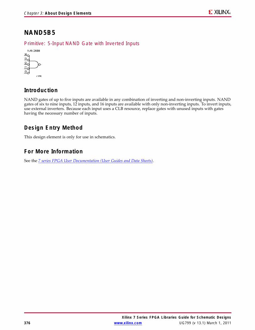
Chapter 3: About Design Elements
NAND5B5Primitive: 5-Input NAND Gate with Inverted Inputs
IntroductionNAND gates of up to five inputs are available in any combination of inverting and non-inverting inputs. NANDgates of six to nine inputs, 12 inputs, and 16 inputs are available with only non-inverting inputs. To invert inputs,use external inverters. Because each input uses a CLB resource, replace gates with unused inputs with gateshaving the necessary number of inputs.
Design Entry MethodThis design element is only for use in schematics.
For More InformationSee the 7 series FPGA User Documentation (User Guides and Data Sheets).
Xilinx 7 Series FPGA Libraries Guide for Schematic Designs376 www.xilinx.com UG799 (v 13.1) March 1, 2011
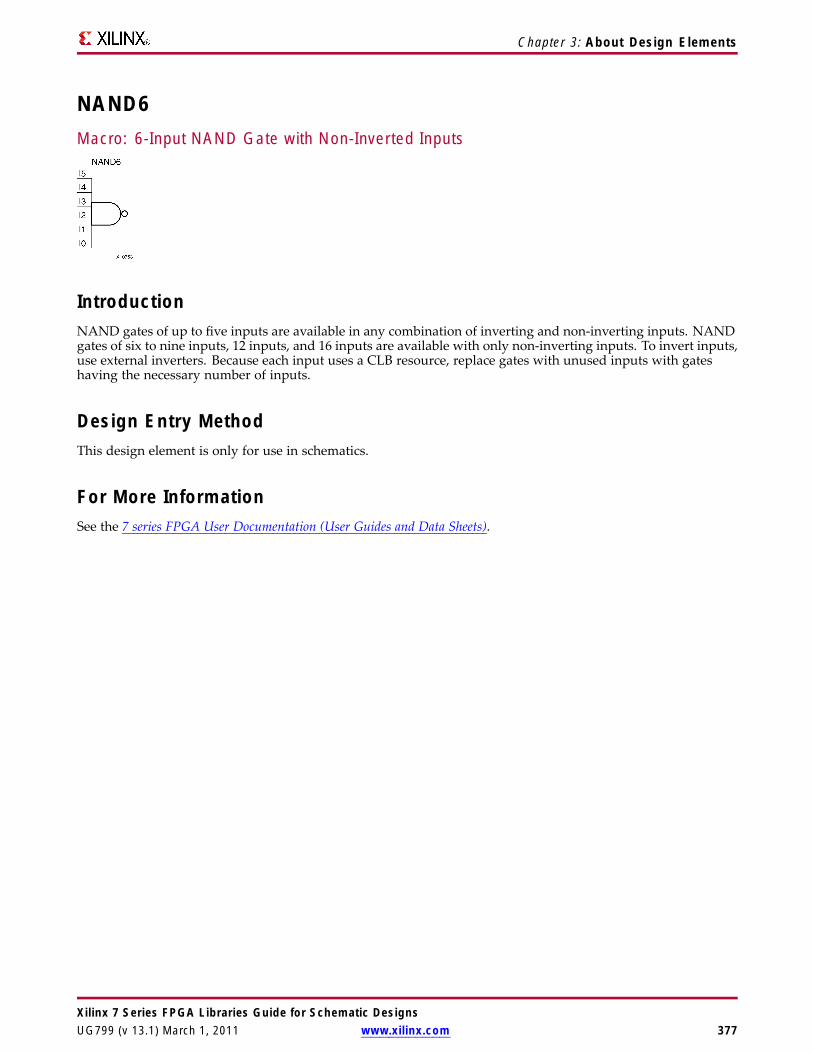
Chapter 3: About Design Elements
NAND6Macro: 6-Input NAND Gate with Non-Inverted Inputs
IntroductionNAND gates of up to five inputs are available in any combination of inverting and non-inverting inputs. NANDgates of six to nine inputs, 12 inputs, and 16 inputs are available with only non-inverting inputs. To invert inputs,use external inverters. Because each input uses a CLB resource, replace gates with unused inputs with gateshaving the necessary number of inputs.
Design Entry MethodThis design element is only for use in schematics.
For More InformationSee the 7 series FPGA User Documentation (User Guides and Data Sheets).
Xilinx 7 Series FPGA Libraries Guide for Schematic DesignsUG799 (v 13.1) March 1, 2011 www.xilinx.com 377
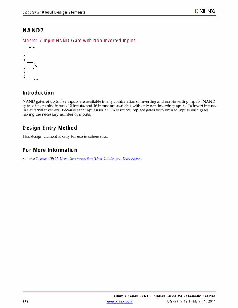
Chapter 3: About Design Elements
NAND7Macro: 7-Input NAND Gate with Non-Inverted Inputs
IntroductionNAND gates of up to five inputs are available in any combination of inverting and non-inverting inputs. NANDgates of six to nine inputs, 12 inputs, and 16 inputs are available with only non-inverting inputs. To invert inputs,use external inverters. Because each input uses a CLB resource, replace gates with unused inputs with gateshaving the necessary number of inputs.
Design Entry MethodThis design element is only for use in schematics.
For More InformationSee the 7 series FPGA User Documentation (User Guides and Data Sheets).
Xilinx 7 Series FPGA Libraries Guide for Schematic Designs378 www.xilinx.com UG799 (v 13.1) March 1, 2011

Chapter 3: About Design Elements
NAND8Macro: 8-Input NAND Gate with Non-Inverted Inputs
IntroductionNAND gates of up to five inputs are available in any combination of inverting and non-inverting inputs. NANDgates of six to nine inputs, 12 inputs, and 16 inputs are available with only non-inverting inputs. To invert inputs,use external inverters. Because each input uses a CLB resource, replace gates with unused inputs with gateshaving the necessary number of inputs.
Design Entry MethodThis design element is only for use in schematics.
For More InformationSee the 7 series FPGA User Documentation (User Guides and Data Sheets).
Xilinx 7 Series FPGA Libraries Guide for Schematic DesignsUG799 (v 13.1) March 1, 2011 www.xilinx.com 379

Chapter 3: About Design Elements
NAND9Macro: 9-Input NAND Gate with Non-Inverted Inputs
IntroductionNAND gates of up to five inputs are available in any combination of inverting and non-inverting inputs. NANDgates of six to nine inputs, 12 inputs, and 16 inputs are available with only non-inverting inputs. To invert inputs,use external inverters. Because each input uses a CLB resource, replace gates with unused inputs with gateshaving the necessary number of inputs.
Design Entry MethodThis design element is only for use in schematics.
For More InformationSee the 7 series FPGA User Documentation (User Guides and Data Sheets).
Xilinx 7 Series FPGA Libraries Guide for Schematic Designs380 www.xilinx.com UG799 (v 13.1) March 1, 2011

Chapter 3: About Design Elements
NOR12Macro: 12-Input NOR Gate with Non-Inverted Inputs
IntroductionNOR gates of up to five inputs are available in any combination of inverting and non-inverting inputs. NORgates of six to nine inputs, 12 inputs, and 16 inputs are available only with non-inverting inputs. To invert someor all inputs, use external inverters. Because each input uses a CLB resource, replace gates with unused inputswith gates having the necessary number of inputs.
Design Entry MethodThis design element is only for use in schematics.
For More InformationSee the 7 series FPGA User Documentation (User Guides and Data Sheets).
Xilinx 7 Series FPGA Libraries Guide for Schematic DesignsUG799 (v 13.1) March 1, 2011 www.xilinx.com 381

Chapter 3: About Design Elements
NOR16Macro: 16-Input NOR Gate with Non-Inverted Inputs
IntroductionNOR gates of up to five inputs are available in any combination of inverting and non-inverting inputs. NORgates of six to nine inputs, 12 inputs, and 16 inputs are available only with non-inverting inputs. To invert someor all inputs, use external inverters. Because each input uses a CLB resource, replace gates with unused inputswith gates having the necessary number of inputs.
Design Entry MethodThis design element is only for use in schematics.
For More InformationSee the 7 series FPGA User Documentation (User Guides and Data Sheets).
Xilinx 7 Series FPGA Libraries Guide for Schematic Designs382 www.xilinx.com UG799 (v 13.1) March 1, 2011

Chapter 3: About Design Elements
NOR2Primitive: 2-Input NOR Gate with Non-Inverted Inputs
IntroductionNOR gates of up to five inputs are available in any combination of inverting and non-inverting inputs. NORgates of six to nine inputs, 12 inputs, and 16 inputs are available only with non-inverting inputs. To invert someor all inputs, use external inverters. Because each input uses a CLB resource, replace gates with unused inputswith gates having the necessary number of inputs.
Design Entry MethodThis design element is only for use in schematics.
For More InformationSee the 7 series FPGA User Documentation (User Guides and Data Sheets).
Xilinx 7 Series FPGA Libraries Guide for Schematic DesignsUG799 (v 13.1) March 1, 2011 www.xilinx.com 383

Chapter 3: About Design Elements
NOR2B1Primitive: 2-Input NOR Gate with 1 Inverted and 1 Non-Inverted Inputs
IntroductionNOR gates of up to five inputs are available in any combination of inverting and non-inverting inputs. NORgates of six to nine inputs, 12 inputs, and 16 inputs are available only with non-inverting inputs. To invert someor all inputs, use external inverters. Because each input uses a CLB resource, replace gates with unused inputswith gates having the necessary number of inputs.
Design Entry MethodThis design element is only for use in schematics.
For More InformationSee the 7 series FPGA User Documentation (User Guides and Data Sheets).
Xilinx 7 Series FPGA Libraries Guide for Schematic Designs384 www.xilinx.com UG799 (v 13.1) March 1, 2011

Chapter 3: About Design Elements
NOR2B2Primitive: 2-Input NOR Gate with Inverted Inputs
IntroductionNOR gates of up to five inputs are available in any combination of inverting and non-inverting inputs. NORgates of six to nine inputs, 12 inputs, and 16 inputs are available only with non-inverting inputs. To invert someor all inputs, use external inverters. Because each input uses a CLB resource, replace gates with unused inputswith gates having the necessary number of inputs.
Design Entry MethodThis design element is only for use in schematics.
For More InformationSee the 7 series FPGA User Documentation (User Guides and Data Sheets).
Xilinx 7 Series FPGA Libraries Guide for Schematic DesignsUG799 (v 13.1) March 1, 2011 www.xilinx.com 385

Chapter 3: About Design Elements
NOR3Primitive: 3-Input NOR Gate with Non-Inverted Inputs
IntroductionNOR gates of up to five inputs are available in any combination of inverting and non-inverting inputs. NORgates of six to nine inputs, 12 inputs, and 16 inputs are available only with non-inverting inputs. To invert someor all inputs, use external inverters. Because each input uses a CLB resource, replace gates with unused inputswith gates having the necessary number of inputs.
Design Entry MethodThis design element is only for use in schematics.
For More InformationSee the 7 series FPGA User Documentation (User Guides and Data Sheets).
Xilinx 7 Series FPGA Libraries Guide for Schematic Designs386 www.xilinx.com UG799 (v 13.1) March 1, 2011

Chapter 3: About Design Elements
NOR3B1Primitive: 3-Input NOR Gate with 1 Inverted and 2 Non-Inverted Inputs
IntroductionNOR gates of up to five inputs are available in any combination of inverting and non-inverting inputs. NORgates of six to nine inputs, 12 inputs, and 16 inputs are available only with non-inverting inputs. To invert someor all inputs, use external inverters. Because each input uses a CLB resource, replace gates with unused inputswith gates having the necessary number of inputs.
Design Entry MethodThis design element is only for use in schematics.
For More InformationSee the 7 series FPGA User Documentation (User Guides and Data Sheets).
Xilinx 7 Series FPGA Libraries Guide for Schematic DesignsUG799 (v 13.1) March 1, 2011 www.xilinx.com 387

Chapter 3: About Design Elements
NOR3B2Primitive: 3-Input NOR Gate with 2 Inverted and 1 Non-Inverted Inputs
IntroductionNOR gates of up to five inputs are available in any combination of inverting and non-inverting inputs. NORgates of six to nine inputs, 12 inputs, and 16 inputs are available only with non-inverting inputs. To invert someor all inputs, use external inverters. Because each input uses a CLB resource, replace gates with unused inputswith gates having the necessary number of inputs.
Design Entry MethodThis design element is only for use in schematics.
For More InformationSee the 7 series FPGA User Documentation (User Guides and Data Sheets).
Xilinx 7 Series FPGA Libraries Guide for Schematic Designs388 www.xilinx.com UG799 (v 13.1) March 1, 2011

Chapter 3: About Design Elements
NOR3B3Primitive: 3-Input NOR Gate with Inverted Inputs
IntroductionNOR gates of up to five inputs are available in any combination of inverting and non-inverting inputs. NORgates of six to nine inputs, 12 inputs, and 16 inputs are available only with non-inverting inputs. To invert someor all inputs, use external inverters. Because each input uses a CLB resource, replace gates with unused inputswith gates having the necessary number of inputs.
Design Entry MethodThis design element is only for use in schematics.
For More InformationSee the 7 series FPGA User Documentation (User Guides and Data Sheets).
Xilinx 7 Series FPGA Libraries Guide for Schematic DesignsUG799 (v 13.1) March 1, 2011 www.xilinx.com 389

Chapter 3: About Design Elements
NOR4Primitive: 4-Input NOR Gate with Non-Inverted Inputs
IntroductionNOR gates of up to five inputs are available in any combination of inverting and non-inverting inputs. NORgates of six to nine inputs, 12 inputs, and 16 inputs are available only with non-inverting inputs. To invert someor all inputs, use external inverters. Because each input uses a CLB resource, replace gates with unused inputswith gates having the necessary number of inputs.
Design Entry MethodThis design element is only for use in schematics.
For More InformationSee the 7 series FPGA User Documentation (User Guides and Data Sheets).
Xilinx 7 Series FPGA Libraries Guide for Schematic Designs390 www.xilinx.com UG799 (v 13.1) March 1, 2011

Chapter 3: About Design Elements
NOR4B1Primitive: 4-Input NOR Gate with 1 Inverted and 3 Non-Inverted Inputs
IntroductionNOR gates of up to five inputs are available in any combination of inverting and non-inverting inputs. NORgates of six to nine inputs, 12 inputs, and 16 inputs are available only with non-inverting inputs. To invert someor all inputs, use external inverters. Because each input uses a CLB resource, replace gates with unused inputswith gates having the necessary number of inputs.
Design Entry MethodThis design element is only for use in schematics.
For More InformationSee the 7 series FPGA User Documentation (User Guides and Data Sheets).
Xilinx 7 Series FPGA Libraries Guide for Schematic DesignsUG799 (v 13.1) March 1, 2011 www.xilinx.com 391

Chapter 3: About Design Elements
NOR4B2Primitive: 4-Input NOR Gate with 2 Inverted and 2 Non-Inverted Inputs
IntroductionNOR gates of up to five inputs are available in any combination of inverting and non-inverting inputs. NORgates of six to nine inputs, 12 inputs, and 16 inputs are available only with non-inverting inputs. To invert someor all inputs, use external inverters. Because each input uses a CLB resource, replace gates with unused inputswith gates having the necessary number of inputs.
Design Entry MethodThis design element is only for use in schematics.
For More InformationSee the 7 series FPGA User Documentation (User Guides and Data Sheets).
Xilinx 7 Series FPGA Libraries Guide for Schematic Designs392 www.xilinx.com UG799 (v 13.1) March 1, 2011

Chapter 3: About Design Elements
NOR4B3Primitive: 4-Input NOR Gate with 3 Inverted and 1 Non-Inverted Inputs
IntroductionNOR gates of up to five inputs are available in any combination of inverting and non-inverting inputs. NORgates of six to nine inputs, 12 inputs, and 16 inputs are available only with non-inverting inputs. To invert someor all inputs, use external inverters. Because each input uses a CLB resource, replace gates with unused inputswith gates having the necessary number of inputs.
Design Entry MethodThis design element is only for use in schematics.
For More InformationSee the 7 series FPGA User Documentation (User Guides and Data Sheets).
Xilinx 7 Series FPGA Libraries Guide for Schematic DesignsUG799 (v 13.1) March 1, 2011 www.xilinx.com 393

Chapter 3: About Design Elements
NOR4B4Primitive: 4-Input NOR Gate with Inverted Inputs
IntroductionNOR gates of up to five inputs are available in any combination of inverting and non-inverting inputs. NORgates of six to nine inputs, 12 inputs, and 16 inputs are available only with non-inverting inputs. To invert someor all inputs, use external inverters. Because each input uses a CLB resource, replace gates with unused inputswith gates having the necessary number of inputs.
Design Entry MethodThis design element is only for use in schematics.
For More InformationSee the 7 series FPGA User Documentation (User Guides and Data Sheets).
Xilinx 7 Series FPGA Libraries Guide for Schematic Designs394 www.xilinx.com UG799 (v 13.1) March 1, 2011

Chapter 3: About Design Elements
NOR5Primitive: 5-Input NOR Gate with Non-Inverted Inputs
IntroductionNOR gates of up to five inputs are available in any combination of inverting and non-inverting inputs. NORgates of six to nine inputs, 12 inputs, and 16 inputs are available only with non-inverting inputs. To invert someor all inputs, use external inverters. Because each input uses a CLB resource, replace gates with unused inputswith gates having the necessary number of inputs.
Design Entry MethodThis design element is only for use in schematics.
For More InformationSee the 7 series FPGA User Documentation (User Guides and Data Sheets).
Xilinx 7 Series FPGA Libraries Guide for Schematic DesignsUG799 (v 13.1) March 1, 2011 www.xilinx.com 395

Chapter 3: About Design Elements
NOR5B1Primitive: 5-Input NOR Gate with 1 Inverted and 4 Non-Inverted Inputs
IntroductionNOR gates of up to five inputs are available in any combination of inverting and non-inverting inputs. NORgates of six to nine inputs, 12 inputs, and 16 inputs are available only with non-inverting inputs. To invert someor all inputs, use external inverters. Because each input uses a CLB resource, replace gates with unused inputswith gates having the necessary number of inputs.
Design Entry MethodThis design element is only for use in schematics.
For More InformationSee the 7 series FPGA User Documentation (User Guides and Data Sheets).
Xilinx 7 Series FPGA Libraries Guide for Schematic Designs396 www.xilinx.com UG799 (v 13.1) March 1, 2011

Chapter 3: About Design Elements
NOR5B2Primitive: 5-Input NOR Gate with 2 Inverted and 3 Non-Inverted Inputs
IntroductionNOR gates of up to five inputs are available in any combination of inverting and non-inverting inputs. NORgates of six to nine inputs, 12 inputs, and 16 inputs are available only with non-inverting inputs. To invert someor all inputs, use external inverters. Because each input uses a CLB resource, replace gates with unused inputswith gates having the necessary number of inputs.
Design Entry MethodThis design element is only for use in schematics.
For More InformationSee the 7 series FPGA User Documentation (User Guides and Data Sheets).
Xilinx 7 Series FPGA Libraries Guide for Schematic DesignsUG799 (v 13.1) March 1, 2011 www.xilinx.com 397
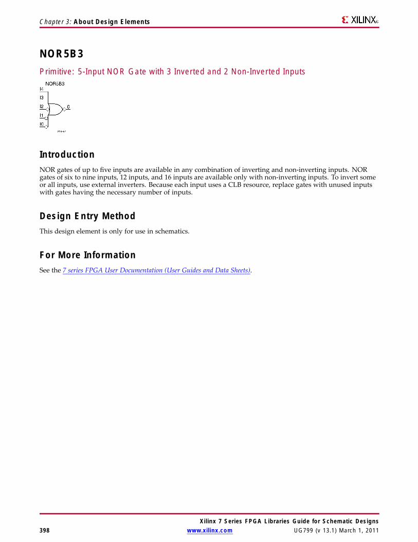
Chapter 3: About Design Elements
NOR5B3Primitive: 5-Input NOR Gate with 3 Inverted and 2 Non-Inverted Inputs
IntroductionNOR gates of up to five inputs are available in any combination of inverting and non-inverting inputs. NORgates of six to nine inputs, 12 inputs, and 16 inputs are available only with non-inverting inputs. To invert someor all inputs, use external inverters. Because each input uses a CLB resource, replace gates with unused inputswith gates having the necessary number of inputs.
Design Entry MethodThis design element is only for use in schematics.
For More InformationSee the 7 series FPGA User Documentation (User Guides and Data Sheets).
Xilinx 7 Series FPGA Libraries Guide for Schematic Designs398 www.xilinx.com UG799 (v 13.1) March 1, 2011

Chapter 3: About Design Elements
NOR5B4Primitive: 5-Input NOR Gate with 4 Inverted and 1 Non-Inverted Inputs
IntroductionNOR gates of up to five inputs are available in any combination of inverting and non-inverting inputs. NORgates of six to nine inputs, 12 inputs, and 16 inputs are available only with non-inverting inputs. To invert someor all inputs, use external inverters. Because each input uses a CLB resource, replace gates with unused inputswith gates having the necessary number of inputs.
Design Entry MethodThis design element is only for use in schematics.
For More InformationSee the 7 series FPGA User Documentation (User Guides and Data Sheets).
Xilinx 7 Series FPGA Libraries Guide for Schematic DesignsUG799 (v 13.1) March 1, 2011 www.xilinx.com 399

Chapter 3: About Design Elements
NOR5B5Primitive: 5-Input NOR Gate with Inverted Inputs
IntroductionNOR gates of up to five inputs are available in any combination of inverting and non-inverting inputs. NORgates of six to nine inputs, 12 inputs, and 16 inputs are available only with non-inverting inputs. To invert someor all inputs, use external inverters. Because each input uses a CLB resource, replace gates with unused inputswith gates having the necessary number of inputs.
Design Entry MethodThis design element is only for use in schematics.
For More InformationSee the 7 series FPGA User Documentation (User Guides and Data Sheets).
Xilinx 7 Series FPGA Libraries Guide for Schematic Designs400 www.xilinx.com UG799 (v 13.1) March 1, 2011

Chapter 3: About Design Elements
NOR6Macro: 6-Input NOR Gate with Non-Inverted Inputs
IntroductionNOR gates of up to five inputs are available in any combination of inverting and non-inverting inputs. NORgates of six to nine inputs, 12 inputs, and 16 inputs are available only with non-inverting inputs. To invert someor all inputs, use external inverters. Because each input uses a CLB resource, replace gates with unused inputswith gates having the necessary number of inputs.
Design Entry MethodThis design element is only for use in schematics.
For More InformationSee the 7 series FPGA User Documentation (User Guides and Data Sheets).
Xilinx 7 Series FPGA Libraries Guide for Schematic DesignsUG799 (v 13.1) March 1, 2011 www.xilinx.com 401
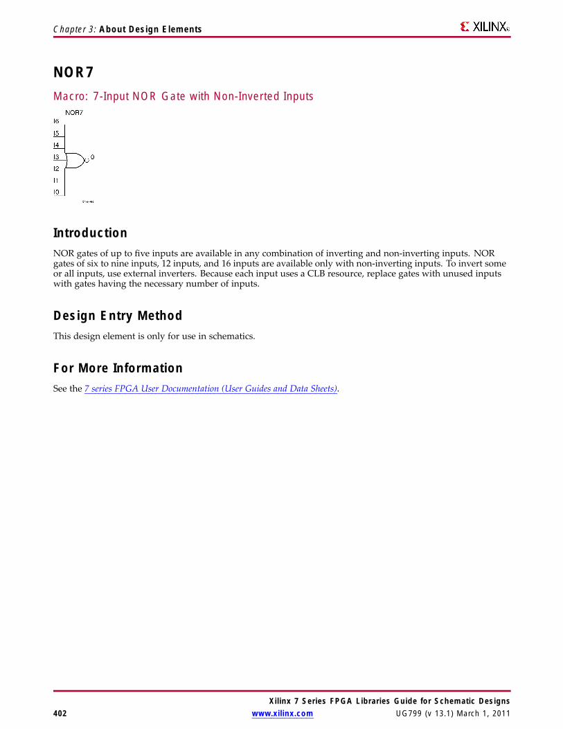
Chapter 3: About Design Elements
NOR7Macro: 7-Input NOR Gate with Non-Inverted Inputs
IntroductionNOR gates of up to five inputs are available in any combination of inverting and non-inverting inputs. NORgates of six to nine inputs, 12 inputs, and 16 inputs are available only with non-inverting inputs. To invert someor all inputs, use external inverters. Because each input uses a CLB resource, replace gates with unused inputswith gates having the necessary number of inputs.
Design Entry MethodThis design element is only for use in schematics.
For More InformationSee the 7 series FPGA User Documentation (User Guides and Data Sheets).
Xilinx 7 Series FPGA Libraries Guide for Schematic Designs402 www.xilinx.com UG799 (v 13.1) March 1, 2011

Chapter 3: About Design Elements
NOR8Macro: 8-Input NOR Gate with Non-Inverted Inputs
IntroductionNOR gates of up to five inputs are available in any combination of inverting and non-inverting inputs. NORgates of six to nine inputs, 12 inputs, and 16 inputs are available only with non-inverting inputs. To invert someor all inputs, use external inverters. Because each input uses a CLB resource, replace gates with unused inputswith gates having the necessary number of inputs.
Design Entry MethodThis design element is only for use in schematics.
For More InformationSee the 7 series FPGA User Documentation (User Guides and Data Sheets).
Xilinx 7 Series FPGA Libraries Guide for Schematic DesignsUG799 (v 13.1) March 1, 2011 www.xilinx.com 403

Chapter 3: About Design Elements
NOR9Macro: 9-Input NOR Gate with Non-Inverted Inputs
IntroductionNOR gates of up to five inputs are available in any combination of inverting and non-inverting inputs. NORgates of six to nine inputs, 12 inputs, and 16 inputs are available only with non-inverting inputs. To invert someor all inputs, use external inverters. Because each input uses a CLB resource, replace gates with unused inputswith gates having the necessary number of inputs.
Design Entry MethodThis design element is only for use in schematics.
For More InformationSee the 7 series FPGA User Documentation (User Guides and Data Sheets).
Xilinx 7 Series FPGA Libraries Guide for Schematic Designs404 www.xilinx.com UG799 (v 13.1) March 1, 2011

Chapter 3: About Design Elements
OBUFPrimitive: Output Buffer
IntroductionThis design element is a simple output buffer used to drive output signals to the FPGA device pins that do notneed to be 3-stated (constantly driven). Either an OBUF, OBUFT, OBUFDS, or OBUFTDS must be connected toevery output port in the design.
This element isolates the internal circuit and provides drive current for signals leaving a chip. It exists ininput/output blocks (IOB). Its output (O) is connected to an OPAD or an IOPAD. The interface standard usedby this element is LVTTL. Also, this element has selectable drive and slew rates using the DRIVE and SLOWor FAST constraints. The defaults are DRIVE=12 mA and SLOW slew.
Port DescriptionsPort Direction Width FunctionO Output 1 Output of OBUF to be connected directly to top-level output
port.
I Input 1 Input of OBUF. Connect to the logic driving the output port.
Design Entry MethodThis design element can be used in schematics.
Available AttributesAttribute Type Allowed Values Default DescriptionIOSTANDARD String See Data Sheet "DEFAULT" Assigns an I/O standard to the element.
For More InformationSee the 7 series FPGA User Documentation (User Guides and Data Sheets).
Xilinx 7 Series FPGA Libraries Guide for Schematic DesignsUG799 (v 13.1) March 1, 2011 www.xilinx.com 405

Chapter 3: About Design Elements
OBUF16Macro: 16-Bit Output Buffer
IntroductionThis design element is a multiple output buffer.
This element isolates the internal circuit and provides drive current for signals leaving a chip. It exists ininput/output blocks (IOB). Its output (O) is connected to an OPAD or an IOPAD. The interface standard usedby this element is LVTTL. Also, this element has selectable drive and slew rates using the DRIVE and SLOWor FAST constraints. The defaults are DRIVE=12 mA and SLOW slew.
Design Entry MethodThis design element can be used in schematics.
Available AttributesAttribute Type Allowed Values Default DescriptionIOSTANDARD String See Data Sheet "DEFAULT" Assigns an I/O standard to the element.
For More InformationSee the 7 series FPGA User Documentation (User Guides and Data Sheets).
Xilinx 7 Series FPGA Libraries Guide for Schematic Designs406 www.xilinx.com UG799 (v 13.1) March 1, 2011

Chapter 3: About Design Elements
OBUF4Macro: 4-Bit Output Buffer
IntroductionThis design element is a multiple output buffer.
This element isolates the internal circuit and provides drive current for signals leaving a chip. It exists ininput/output blocks (IOB). Its output (O) is connected to an OPAD or an IOPAD. The interface standard usedby this element is LVTTL. Also, this element has selectable drive and slew rates using the DRIVE and SLOWor FAST constraints. The defaults are DRIVE=12 mA and SLOW slew.
Design Entry MethodThis design element can be used in schematics.
Available AttributesAttribute Type Allowed Values Default DescriptionIOSTANDARD String See Data Sheet "DEFAULT" Assigns an I/O standard to the element.
For More InformationSee the 7 series FPGA User Documentation (User Guides and Data Sheets).
Xilinx 7 Series FPGA Libraries Guide for Schematic DesignsUG799 (v 13.1) March 1, 2011 www.xilinx.com 407

Chapter 3: About Design Elements
OBUF8Macro: 8-Bit Output Buffer
IntroductionThis design element is a multiple output buffer.
This element isolates the internal circuit and provides drive current for signals leaving a chip. It exists ininput/output blocks (IOB). Its output (O) is connected to an OPAD or an IOPAD. The interface standard usedby this element is LVTTL. Also, this element has selectable drive and slew rates using the DRIVE and SLOWor FAST constraints. The defaults are DRIVE=12 mA and SLOW slew.
Design Entry MethodThis design element can be used in schematics.
Available AttributesAttribute Type Allowed Values Default DescriptionIOSTANDARD String See Data Sheet "DEFAULT" Assigns an I/O standard to the element.
For More InformationSee the 7 series FPGA User Documentation (User Guides and Data Sheets).
Xilinx 7 Series FPGA Libraries Guide for Schematic Designs408 www.xilinx.com UG799 (v 13.1) March 1, 2011

Chapter 3: About Design Elements
OBUFDSPrimitive: Differential Signaling Output Buffer
IntroductionThis design element is a single output buffer that supports low-voltage, differential signaling (1.8 v CMOS).OBUFDS isolates the internal circuit and provides drive current for signals leaving the chip. Its output isrepresented as two distinct ports (O and OB), one deemed the "master" and the other the "slave." The master andthe slave are opposite phases of the same logical signal (for example, MYNET and MYNETB).
Logic TableInputs Outputs
I O OB0 0 1
1 1 0
Port DescriptionsPort Direction Width FunctionO Output 1 Diff_p output (connect directly to top level port)
OB Output 1 Diff_n output (connect directly to top level port)
I Input 1 Buffer input
Design Entry MethodThis design element can be used in schematics.
Available Attributes
Attribute TypeAllowedValues Default Description
IOSTANDARD String See Data Sheet "DEFAULT" Assigns an I/O standard to the element.
For More InformationSee the 7 series FPGA User Documentation (User Guides and Data Sheets).
Xilinx 7 Series FPGA Libraries Guide for Schematic DesignsUG799 (v 13.1) March 1, 2011 www.xilinx.com 409

Chapter 3: About Design Elements
OBUFTPrimitive: 3-State Output Buffer with Active Low Output Enable
IntroductionThis design element is a single, 3-state output buffer with input I, output O, and active-Low output enables (T).This element uses the LVTTL standard and has selectable drive and slew rates using the DRIVE and SLOW orFAST constraints. The defaults are DRIVE=12 mA and SLOW slew.
When T is Low, data on the inputs of the buffers is transferred to the corresponding outputs. When T is High, theoutput is high impedance (off or Z state). OBUFTs are generally used when a single-ended output is neededwith a 3-state capability, such as the case when building bidirectional I/O.
Logic TableInputs Outputs
T I O1 X Z
0 1 1
0 0 0
Port DescriptionsPort Direction Width FunctionO Output 1 Buffer output (connect directly to top-level port)
I Input 1 Buffer input
T Input 1 3-state enable input
Design Entry MethodThis design element can be used in schematics.
Available AttributesAttribute Type Allowed Values Default DescriptionIOSTANDARD String See Data Sheet "DEFAULT" Assigns an I/O standard to the element.
For More Information
Xilinx 7 Series FPGA Libraries Guide for Schematic Designs410 www.xilinx.com UG799 (v 13.1) March 1, 2011

Chapter 3: About Design Elements
OBUFT16Macro: 16-Bit 3-State Output Buffer with Active Low Output Enable
IntroductionThis design element is a multiple, 3-state output buffer with input I, output O, and active-Low output enables(T). This element uses the LVTTL standard and has selectable drive and slew rates using the DRIVE and SLOWor FAST constraints. The defaults are DRIVE=12 mA and SLOW slew.
When T is Low, data on the inputs of the buffers is transferred to the corresponding outputs. When T is High, theoutput is high impedance (off or Z state). OBUFTs are generally used when a single-ended output is neededwith a 3-state capability, such as the case when building bidirectional I/O.
Logic TableInputs Outputs
T I O1 X Z
0 1 1
0 0 0
Design Entry MethodThis design element is only for use in schematics.
Available AttributesAttribute Type Allowed Values Default DescriptionIOSTANDARD String See Data Sheet "DEFAULT" Assigns an I/O standard to the element.
For More InformationSee the 7 series FPGA User Documentation (User Guides and Data Sheets).
Xilinx 7 Series FPGA Libraries Guide for Schematic DesignsUG799 (v 13.1) March 1, 2011 www.xilinx.com 411

Chapter 3: About Design Elements
OBUFT4Macro: 4-Bit 3-State Output Buffers with Active-Low Output Enable
IntroductionThis design element is a multiple, 3-state output buffer with input I, output O, and active-Low output enables(T). This element uses the LVTTL standard and has selectable drive and slew rates using the DRIVE and SLOWor FAST constraints. The defaults are DRIVE=12 mA and SLOW slew.
When T is Low, data on the inputs of the buffers is transferred to the corresponding outputs. When T is High, theoutput is high impedance (off or Z state). OBUFTs are generally used when a single-ended output is neededwith a 3-state capability, such as the case when building bidirectional I/O.
Logic TableInputs Outputs
T I O1 X Z
0 1 1
0 0 0
Design Entry MethodThis design element is only for use in schematics.
Available AttributesAttribute Type Allowed Values Default DescriptionIOSTANDARD String See Data Sheet "DEFAULT" Assigns an I/O standard to the element.
For More InformationSee the 7 series FPGA User Documentation (User Guides and Data Sheets).
Xilinx 7 Series FPGA Libraries Guide for Schematic Designs412 www.xilinx.com UG799 (v 13.1) March 1, 2011

Chapter 3: About Design Elements
OBUFT8Macro: 8-Bit 3-State Output Buffers with Active-Low Output Enable
IntroductionThis design element is a multiple, 3-state output buffer with input I, output O, and active-Low output enables(T). This element uses the LVTTL standard and has selectable drive and slew rates using the DRIVE and SLOWor FAST constraints. The defaults are DRIVE=12 mA and SLOW slew.
When T is Low, data on the inputs of the buffers is transferred to the corresponding outputs. When T is High, theoutput is high impedance (off or Z state). OBUFTs are generally used when a single-ended output is neededwith a 3-state capability, such as the case when building bidirectional I/O.
Logic TableInputs Outputs
T I O1 X Z
0 1 1
0 0 0
Design Entry MethodThis design element is only for use in schematics.
Available AttributesAttribute Type Allowed Values Default DescriptionIOSTANDARD String See Data Sheet "DEFAULT" Assigns an I/O standard to the element.
For More InformationSee the 7 series FPGA User Documentation (User Guides and Data Sheets).
Xilinx 7 Series FPGA Libraries Guide for Schematic DesignsUG799 (v 13.1) March 1, 2011 www.xilinx.com 413

Chapter 3: About Design Elements
OBUFTDSPrimitive: 3-State Output Buffer with Differential Signaling, Active-Low Output Enable
IntroductionThis design element is an output buffer that supports low-voltage, differential signaling. For the OBUFTDS,a design level interface signal is represented as two distinct ports (O and OB), one deemed the "master" andthe other the "slave." The master and the slave are opposite phases of the same logical signal (for example,MYNET_P and MYNET_N).
Logic TableInputs Outputs
I T O OBX 1 Z Z
0 0 0 1
1 0 1 0
Port DescriptionsPort Direction Width FunctionO Output 1 Diff_p output (connect directly to top level port)
OB Output 1 Diff_n output (connect directly to top level port)
I Input 1 Buffer input
T Input 1 3-state enable input
Design Entry MethodThis design element can be used in schematics.
Available AttributesAttribute Type Allowed Values Default DescriptionIOSTANDARD String See Data Sheet "DEFAULT" Assigns an I/O standard to the element.
For More Information
Xilinx 7 Series FPGA Libraries Guide for Schematic Designs414 www.xilinx.com UG799 (v 13.1) March 1, 2011

Chapter 3: About Design Elements
ODDRPrimitive: Dedicated Dual Data Rate (DDR) Output Register
IntroductionThis design element is a dedicated output register for use in transmitting dual data rate (DDR) signals fromFPGA devices. The ODDR primitive’s interface with the FPGA fabric are not limited to opposite edges. TheODDR is available with modes that allow data to be presented from the FPGA fabric at the same clock edge. Thisfeature allows designers to avoid additional timing complexities and CLB usage. In addition, the ODDR worksin conjunction with SelectIO™ features.
ODDR Modes
This element has two modes of operation. These modes are set by the DDR_CLK_EDGE attribute.
• OPPOSITE_EDGE mode - The data transmit interface uses the classic DDR methodology. Given a data andclock at pin D1-2 and C respectively, D1 is sampled at every positive edge of clock C, and D2 is sampled atevery negative edge of clock C. Q changes every clock edge.
• SAME_EDGE mode - Data is still transmitted at the output of the ODDR by opposite edges of clock C.However, the two inputs to the ODDR are clocked with a positive clock edge of clock signal C and an extraregister is clocked with a negative clock edge of clock signal C. Using this feature, DDR data can now bepresented into the ODDR at the same clock edge.
Port DescriptionsPort Type Width FunctionQ Output 1 Data Output (DDR) - The ODDR output that connects to the IOB
pad.
C Input 1 Clock Input - The C pin represents the clock input pin.
CE Input 1 Clock Enable Input - When asserted High, this port enables theclock input on port C.
D1 : D2 Input 1 (each) Data Input - This pin is where the DDR data is presented intothe ODDR module.
R Input 1 Reset - Depends on how SRTYPE is set.
S Input 1 Set - Active High asynchronous set pin. This pin can also beSynchronous depending on the SRTYPE attribute.
Design Entry MethodThis design element can be used in schematics.
Xilinx 7 Series FPGA Libraries Guide for Schematic DesignsUG799 (v 13.1) March 1, 2011 www.xilinx.com 415

Chapter 3: About Design Elements
Available AttributesAttribute Type Allowed Values Default DescriptionDDR_CLK_EDGE
String "OPPOSITE_EDGE","SAME_EDGE"
"OPPOSITE_EDGE"
DDR clock mode recovery modeselection.
INIT Integer 0, 1 1 Q initialization value.
SRTYPE String "SYNC", "ASYNC" "SYNC" Set/Reset type selection.
For More InformationSee the 7 series FPGA User Documentation (User Guides and Data Sheets).
Xilinx 7 Series FPGA Libraries Guide for Schematic Designs416 www.xilinx.com UG799 (v 13.1) March 1, 2011

Chapter 3: About Design Elements
ODELAYE2
Primitive: Output Fixed or Variable Delay Element
IntroductionThis design element can be used to provide a fixed delay or an adjustable delay to the output path of the 7series FPGA. This delay can be useful for the purpose of external data alignment, external phase offset andsimultaneous switching noise (SSN) mitigation, as well as allowing for the tracking of data alignment overprocess, temperature, and voltage (PVT). When used in conjunction with the IDELAYCTRL component circuitry,can provide precise time increments of delay. When used in variable mode, the input path can be adjusted forincreasing and decreasing amounts of delay. The ODELAY is not available on the High Range banks in the 7series devices.
Port Descriptions
Port Type Width FunctionC Input 1 All control inputs to ODELAYE2 primitive (RST, CE, LD, and INC)
are synchronous to the clock input (C). A clock must be connectedto this port when the ODELAYE2 is configured in "VARIABLE","VAR_LOAD", or "VAR_LOAD_PIPE" mode. C can be locally inverted,and must be supplied by a global or regional clock buffer. This clockshould be connected to the same clock in the SelectIO™ logic resources(when using ISERDESE2 and OSERDESE2, C is connected to CLKDIV).
CE Input 1 Active high enable increment/decrement function.
CINVCTRL Input 1 The CINVCTRL pin is used for dynamically switching the polarity ofC pin. This is for use in applications when glitches are not an issue.When switching the polarity, do not use the ODELAYE2 control pinsfor two clock cycles.
CLKIN Input 1 Clock Access into the ODELAYE2.
CNTVALUEIN<4:0>
Input 5 Counter value from FPGA logic for dynamically loadable tap valueinput.
CNTVALUEOUT<4:0>
Output 5 The CNTVALUEOUT pins are used for reporting the dynamicallyswitching value of the delay element. CNTVALUEOUT is only availablewhen ODELAYE2 is in "VAR_LOAD" or "VAR_LOAD_PIPE" mode.
DATAOUT Output 1 Delayed data from the two data input ports. DATAOUT connects toan I/O port.
Xilinx 7 Series FPGA Libraries Guide for Schematic DesignsUG799 (v 13.1) March 1, 2011 www.xilinx.com 417

Chapter 3: About Design Elements
Port Type Width FunctionINC Input 1 Increment or decrement number of tap delays
LD Input 1 Load initial value or loaded value to the counter.
LDPIPEEN Input 1 Enable PIPELINE register to load data from LD pins.
ODATAIN Input 1 The ODATAIN input is driven by the OSERDESE2 or output register.The ODATAIN drives the DATAOUT port which is connected to eitheran I/O or clock source with a delay set by the ODELAY_VALUE.
REGRST Input 1 When in "VARIABLE" mode, the ODELAYE2 reset signal resets thedelay element to a value set by the ODELAY_VALUE attribute. If thisattribute is not specified, a value of zero is assumed. The REGRSTsignal is an active-high reset and is synchronous to the input clocksignal (C). When in "VAR_LOAD" or "VAR_LOAD_PIPE" mode, theODELAYE2 reset signal resets the delay element to a value set by theCNTVALUEIN. The value present at CNTVALUEIN will be the newtap value. As a results of this functionality the ODELAY_VALUEattribute is ignored.
Design Entry MethodThis design element can be used in schematics.
Available AttributesAttribute Type Allowed Values Default DescriptionCINVCTRL_SEL STRING FALSE, TRUE FALSE Dynamically inverts the Clock (C)
polarity.
DELAY_SRC STRING ODATAIN, CLKIN ODATAIN Select the data input source:
• "ODATAIN": ODELAYE2 chaininput is ODATAIN
• "CLKIN": ODELAYE2 chain inputis CLKIN
HIGH_PERFORMANCE_MODE
STRING TRUE, FALSE TRUE When TRUE, this attribute reduces theoutput jitter. When FALSE, reducespower consumption. The difference inpower consumption is quantified in theXilinx Power Estimator/Analyzer tools.
ODELAY_TYPE STRING FIXED, VAR_LOAD,VAR_LOAD_PIPE,VARIABLE
FIXED Sets the type of tap delay line.
• "FIXED": Sets a static delay value.
• "VARIABLE": Dynamically adjust(incement/decrement) delay value
• "VAR_LOAD": Dynamically loadstap values.
• "VAR_LOAD_PIPE": Pipelineddynamically loadable tap values.
ODELAY_VALUE DECIMAL 0, 1, 2, 3, 4, 5, 6, 7, 8, 9,10, 11, 12, 13, 14, 15, 16,17, 18, 19, 20, 21, 22, 23,24, 25, 26, 27, 28, 29, 30,31
0 Specifies the fixed number of delaytaps in fixed mode or the initial startingnumber of taps in VARIABLE mode(input path). When ODELAY_TYPE isset to VAR_LOADorVAR_LOAD_PIPEmode, this value is ignored.
Xilinx 7 Series FPGA Libraries Guide for Schematic Designs418 www.xilinx.com UG799 (v 13.1) March 1, 2011

Chapter 3: About Design Elements
Attribute Type Allowed Values Default DescriptionPIPE_SEL STRING FALSE, TRUE FALSE Select pipelined mode.
REFCLK_FREQUENCY
1 significantdigit FLOAT
190.0 to 210.0 200.0 Sets the tap value (in MHz) usedby the timing analyzer for statictiming analysis and functional/timingsimulation. The frequency of REFCLKmust be within the given datasheetrange to guarantee the tap-delay valueand performance.
SIGNAL_PATTERN
STRING DATA, CLOCK DATA Causes the timing analyzer to accountfor the appropriate amount ofdelay-chain jitter in the data or clockpath.
For More Information• See the 7 series FPGA SelectIO Resources User Guide.
• See the 7 series FPGA Data Sheet DC and Switching Characteristics.
Xilinx 7 Series FPGA Libraries Guide for Schematic DesignsUG799 (v 13.1) March 1, 2011 www.xilinx.com 419

Chapter 3: About Design Elements
OFDMacro: Output D Flip-Flop
IntroductionThis design element is a single output D flip-flop.
The outputs are connected to OPADs or IOPADs. The data on the (D) inputs is loaded into the flip-flops duringthe Low-to-High clock (C) transition and appears on the (Q) outputs.
This flip-flop is asynchronously cleared, outputs Low, when power is applied. For FPGA devices, power-onconditions are simulated when global set/reset (GSR) is active. GSR defaults to active-High but can be invertedby adding an inverter in front of the GSR input of the appropriate STARTUP_architecture symbol.
Logic TableInputs Outputs
D C QD ↑ D
Design Entry MethodThis design element is only for use in schematics.
For More InformationSee the 7 series FPGA User Documentation (User Guides and Data Sheets).
Xilinx 7 Series FPGA Libraries Guide for Schematic Designs420 www.xilinx.com UG799 (v 13.1) March 1, 2011

Chapter 3: About Design Elements
OFD_1Macro: Output D Flip-Flop with Inverted Clock
IntroductionThe design element is located in an input/output block (IOB). The output (Q) of the D flip-flop is connected to anOPAD or an IOPAD. The data on the (D) input is loaded into the flip-flop during the High-to-Low clock (C)transition and appears on the (Q) output.
This flip-flop is asynchronously cleared, outputs Low, when power is applied. For FPGA devices, power-onconditions are simulated when global set/reset (GSR) is active. GSR defaults to active-High but can be invertedby adding an inverter in front of the GSR input of the appropriate STARTUP_architecture symbol.
Logic TableInputs Outputs
D C QD ↓ D
Design Entry MethodThis design element is only for use in schematics.
For More InformationSee the 7 series FPGA User Documentation (User Guides and Data Sheets).
Xilinx 7 Series FPGA Libraries Guide for Schematic DesignsUG799 (v 13.1) March 1, 2011 www.xilinx.com 421

Chapter 3: About Design Elements
OFD16Macro: 16-Bit Output D Flip-Flop
IntroductionThis design element is a multiple output D flip-flop.
The outputs are connected to OPADs or IOPADs. The data on the (D) inputs is loaded into the flip-flops duringthe Low-to-High clock (C) transition and appears on the (Q) outputs.
This flip-flop is asynchronously cleared, outputs Low, when power is applied. For FPGA devices, power-onconditions are simulated when global set/reset (GSR) is active. GSR defaults to active-High but can be invertedby adding an inverter in front of the GSR input of the appropriate STARTUP_architecture symbol.
Logic TableInputs Outputs
D C QD ↑ D
Design Entry MethodThis design element is only for use in schematics.
For More InformationSee the 7 series FPGA User Documentation (User Guides and Data Sheets).
Xilinx 7 Series FPGA Libraries Guide for Schematic Designs422 www.xilinx.com UG799 (v 13.1) March 1, 2011

Chapter 3: About Design Elements
OFD4Macro: 4-Bit Output D Flip-Flop
IntroductionThis design element is a multiple output D flip-flop.
The outputs are connected to OPADs or IOPADs. The data on the (D) inputs is loaded into the flip-flops duringthe Low-to-High clock (C) transition and appears on the (Q) outputs.
This flip-flop is asynchronously cleared, outputs Low, when power is applied. For FPGA devices, power-onconditions are simulated when global set/reset (GSR) is active. GSR defaults to active-High but can be invertedby adding an inverter in front of the GSR input of the appropriate STARTUP_architecture symbol.
Logic TableInputs Outputs
D C QD ↑ D
Design Entry MethodThis design element is only for use in schematics.
For More InformationSee the 7 series FPGA User Documentation (User Guides and Data Sheets).
Xilinx 7 Series FPGA Libraries Guide for Schematic DesignsUG799 (v 13.1) March 1, 2011 www.xilinx.com 423

Chapter 3: About Design Elements
OFD8Macro: 8-Bit Output D Flip-Flop
IntroductionThis design element is a multiple output D flip-flop.
The outputs are connected to OPADs or IOPADs. The data on the (D) inputs is loaded into the flip-flops duringthe Low-to-High clock (C) transition and appears on the (Q) outputs.
This flip-flop is asynchronously cleared, outputs Low, when power is applied. For FPGA devices, power-onconditions are simulated when global set/reset (GSR) is active. GSR defaults to active-High but can be invertedby adding an inverter in front of the GSR input of the appropriate STARTUP_architecture symbol.
Logic TableInputs Outputs
D C QD ↑ D
Design Entry MethodThis design element is only for use in schematics.
For More InformationSee the 7 series FPGA User Documentation (User Guides and Data Sheets).
Xilinx 7 Series FPGA Libraries Guide for Schematic Designs424 www.xilinx.com UG799 (v 13.1) March 1, 2011

Chapter 3: About Design Elements
OFDEMacro: D Flip-Flop with Active-High Enable Output Buffers
IntroductionThis is a single D flip-flop whose output is enabled by a 3-state buffer. The flip-flop data output (Q) is connectedto the input of output buffer (OBUFE). The OBUFE output (O) is connected to an OPAD or IOPAD. The data onthe data input (D) is loaded into the flip-flop during the Low-to-High clock (C) transition. When the active-Highenable input (E) is High, the data on the flip-flop output (Q) appears on the OBUFE (O) output. When (E) isLow, the output is high impedance (Z state or Off).
This flip-flop is asynchronously cleared, outputs Low, when power is applied. For FPGA devices, power-onconditions are simulated when global set/reset (GSR) is active. GSR defaults to active-High but can be invertedby adding an inverter in front of the GSR input of the appropriate STARTUP_architecture symbol.
Logic TableInputs Output
E D C O0 X X Z
1 Dn ↑ Dn
Design Entry MethodThis design element is only for use in schematics.
For More InformationSee the 7 series FPGA User Documentation (User Guides and Data Sheets).
Xilinx 7 Series FPGA Libraries Guide for Schematic DesignsUG799 (v 13.1) March 1, 2011 www.xilinx.com 425
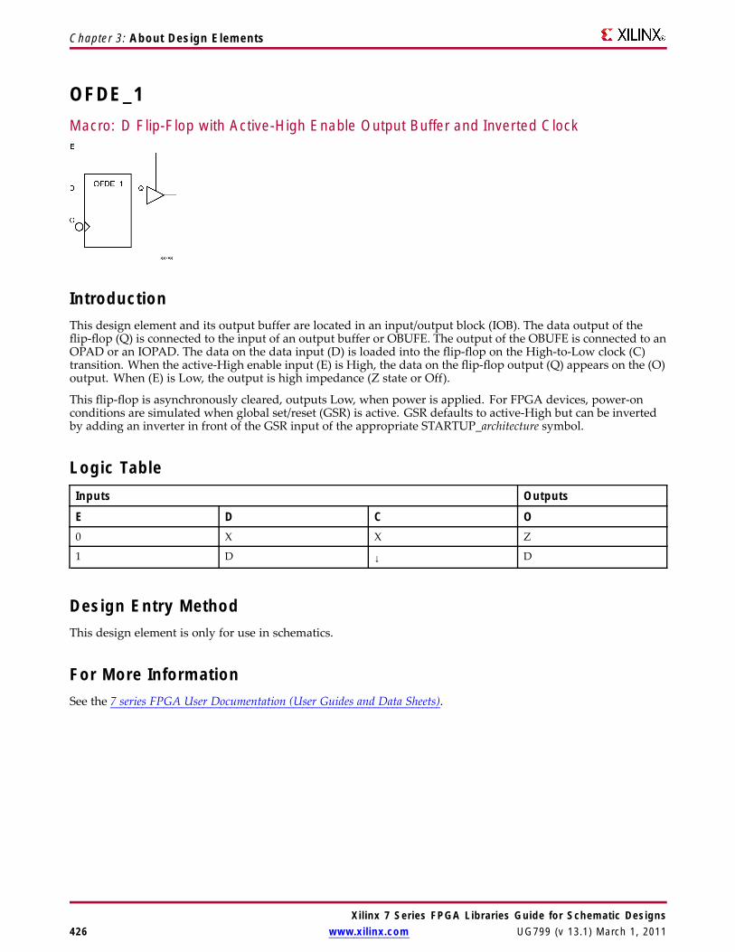
Chapter 3: About Design Elements
OFDE_1Macro: D Flip-Flop with Active-High Enable Output Buffer and Inverted Clock
IntroductionThis design element and its output buffer are located in an input/output block (IOB). The data output of theflip-flop (Q) is connected to the input of an output buffer or OBUFE. The output of the OBUFE is connected to anOPAD or an IOPAD. The data on the data input (D) is loaded into the flip-flop on the High-to-Low clock (C)transition. When the active-High enable input (E) is High, the data on the flip-flop output (Q) appears on the (O)output. When (E) is Low, the output is high impedance (Z state or Off).
This flip-flop is asynchronously cleared, outputs Low, when power is applied. For FPGA devices, power-onconditions are simulated when global set/reset (GSR) is active. GSR defaults to active-High but can be invertedby adding an inverter in front of the GSR input of the appropriate STARTUP_architecture symbol.
Logic TableInputs Outputs
E D C O0 X X Z
1 D ↓ D
Design Entry MethodThis design element is only for use in schematics.
For More InformationSee the 7 series FPGA User Documentation (User Guides and Data Sheets).
Xilinx 7 Series FPGA Libraries Guide for Schematic Designs426 www.xilinx.com UG799 (v 13.1) March 1, 2011

Chapter 3: About Design Elements
OFDE16Macro: 16-Bit D Flip-Flop with Active-High Enable Output Buffers
IntroductionThis is a multiple D flip-flop whose outputs are enabled by 3-state buffers. The flip-flop data outputs (Q) areconnected to the inputs of output buffers (OBUFE). The OBUFE outputs (O) are connected to OPADs or IOPADs.The data on the data inputs (D) is loaded into the flip-flops during the Low-to-High clock (C) transition. Whenthe active-High enable inputs (E) are High, the data on the flip-flop outputs (Q) appears on the OBUFE outputs(O). When (E) is Low, outputs are high impedance (Z state or Off).
This flip-flop is asynchronously cleared, outputs Low, when power is applied. For FPGA devices, power-onconditions are simulated when global set/reset (GSR) is active. GSR defaults to active-High but can be invertedby adding an inverter in front of the GSR input of the appropriate STARTUP_architecture symbol.
Logic TableInputs Outputs
E D C O0 X X Z
1 Dn ↑ Dn
Design Entry MethodThis design element is only for use in schematics.
For More InformationSee the 7 series FPGA User Documentation (User Guides and Data Sheets).
Xilinx 7 Series FPGA Libraries Guide for Schematic DesignsUG799 (v 13.1) March 1, 2011 www.xilinx.com 427

Chapter 3: About Design Elements
OFDE4Macro: 4-Bit D Flip-Flop with Active-High Enable Output Buffers
IntroductionThis is a multiple D flip-flop whose outputs are enabled by 3-state buffers. The flip-flop data outputs (Q) areconnected to the inputs of output buffers (OBUFE). The OBUFE outputs (O) are connected to OPADs or IOPADs.The data on the data inputs (D) is loaded into the flip-flops during the Low-to-High clock (C) transition. Whenthe active-High enable inputs (E) are High, the data on the flip-flop outputs (Q) appears on the OBUFE outputs(O). When (E) is Low, outputs are high impedance (Z state or Off).
This flip-flop is asynchronously cleared, outputs Low, when power is applied. For FPGA devices, power-onconditions are simulated when global set/reset (GSR) is active. GSR defaults to active-High but can be invertedby adding an inverter in front of the GSR input of the appropriate STARTUP_architecture symbol.
Logic TableInputs Outputs
E D C O0 X X Z
1 Dn ↑ Dn
Design Entry MethodThis design element is only for use in schematics.
For More InformationSee the 7 series FPGA User Documentation (User Guides and Data Sheets).
Xilinx 7 Series FPGA Libraries Guide for Schematic Designs428 www.xilinx.com UG799 (v 13.1) March 1, 2011

Chapter 3: About Design Elements
OFDE8Macro: 8-Bit D Flip-Flop with Active-High Enable Output Buffers
IntroductionThis is a multiple D flip-flop whose outputs are enabled by 3-state buffers. The flip-flop data outputs (Q) areconnected to the inputs of output buffers (OBUFE). The OBUFE outputs (O) are connected to OPADs or IOPADs.The data on the data inputs (D) is loaded into the flip-flops during the Low-to-High clock (C) transition. Whenthe active-High enable inputs (E) are High, the data on the flip-flop outputs (Q) appears on the OBUFE outputs(O). When (E) is Low, outputs are high impedance (Z state or Off).
This flip-flop is asynchronously cleared, outputs Low, when power is applied. For FPGA devices, power-onconditions are simulated when global set/reset (GSR) is active. GSR defaults to active-High but can be invertedby adding an inverter in front of the GSR input of the appropriate STARTUP_architecture symbol.
Logic TableInputs Outputs
E D C O0 X X Z
1 Dn ↑ Dn
Design Entry MethodThis design element is only for use in schematics.
For More InformationSee the 7 series FPGA User Documentation (User Guides and Data Sheets).
Xilinx 7 Series FPGA Libraries Guide for Schematic DesignsUG799 (v 13.1) March 1, 2011 www.xilinx.com 429

Chapter 3: About Design Elements
OFDIMacro: Output D Flip-Flop (Asynchronous Preset)
IntroductionThe design element is contained in an input/output block (IOB). The output (Q) of the (D) flip-flop is connectedto an OPAD or an IOPAD. The data on the (D) input is loaded into the flip-flop during the Low-to-High clock (C)transition and appears at the output (Q).
This flip-flop is asynchronously preset, output High, when power is applied. For FPGA devices, power-onconditions are simulated when global set/reset (GSR) is active. GSR defaults to active-High but can be invertedby adding an inverter in front of the GSR input of the appropriate STARTUP_architecture symbol.
Logic TableInputs Outputs
D C QD ↑ D
Design Entry MethodThis design element is only for use in schematics.
For More InformationSee the 7 series FPGA User Documentation (User Guides and Data Sheets).
Xilinx 7 Series FPGA Libraries Guide for Schematic Designs430 www.xilinx.com UG799 (v 13.1) March 1, 2011

Chapter 3: About Design Elements
OFDI_1Macro: Output D Flip-Flop with Inverted Clock (Asynchronous Preset)
IntroductionThis design element exists in an input/output block (IOB). The (D) flip-flop output (Q) is connected to an OPADor an IOPAD. The data on the (D) input is loaded into the flip-flop during the High-to-Low clock (C) transitionand appears on the (Q) output.
This flip-flop is asynchronously preset, output High, when power is applied. For FPGA devices, power-onconditions are simulated when global set/reset (GSR) is active. GSR defaults to active-High but can be invertedby adding an inverter in front of the GSR input of the appropriate STARTUP_architecture symbol.
Logic TableInputs Outputs
D C QD ↓ D
Design Entry MethodThis design element is only for use in schematics.
For More InformationSee the 7 series FPGA User Documentation (User Guides and Data Sheets).
Xilinx 7 Series FPGA Libraries Guide for Schematic DesignsUG799 (v 13.1) March 1, 2011 www.xilinx.com 431

Chapter 3: About Design Elements
OFDTMacro: D Flip-Flop with Active-Low 3-State Output Buffer
IntroductionThis design element is a single D flip-flops whose output is enabled by a 3-state buffer.
The data outputs (Q) of the flip-flops are connected to the inputs of output buffers (OBUFT). The outputs of theOBUFTs (O) are connected to OPADs or IOPADs. The data on the data inputs (D) is loaded into the flip-flopsduring the Low-to-High clock (C) transition. When the active-Low enable inputs (T) are Low, the data on theflip-flop outputs (Q) appears on the (O) outputs. When (T) is High, outputs are high impedance (Off).
This flip-flop is asynchronously cleared, outputs Low, when power is applied. For FPGA devices, power-onconditions are simulated when global set/reset (GSR) is active. GSR defaults to active-High but can be invertedby adding an inverter in front of the GSR input of the appropriate STARTUP_architecture symbol.
Logic TableInputs Outputs
T D C O1 X X Z
0 D ↑ D
Design Entry MethodThis design element is only for use in schematics.
For More InformationSee the 7 series FPGA User Documentation (User Guides and Data Sheets).
Xilinx 7 Series FPGA Libraries Guide for Schematic Designs432 www.xilinx.com UG799 (v 13.1) March 1, 2011

Chapter 3: About Design Elements
OFDT_1Macro: D Flip-Flop with Active-Low 3-State Output Buffer and Inverted Clock
IntroductionThe design element and its output buffer are located in an input/output block (IOB). The flip-flop data output(Q) is connected to the input of an output buffer (OBUFT). The OBUFT output is connected to an OPAD or anIOPAD. The data on the data input (D) is loaded into the flip-flop on the High-to-Low clock (C) transition.When the active-Low enable input (T) is Low, the data on the flip-flop output (Q) appears on the (O) output.When (T) is High, the output is high impedance (Off).
This flip-flop is asynchronously cleared, outputs Low, when power is applied. For FPGA devices, power-onconditions are simulated when global set/reset (GSR) is active. GSR defaults to active-High but can be invertedby adding an inverter in front of the GSR input of the appropriate STARTUP_architecture symbol.
Logic TableInputs Outputs
T D C O1 X X Z
0 D ↓ D
Design Entry MethodThis design element is only for use in schematics.
For More InformationSee the 7 series FPGA User Documentation (User Guides and Data Sheets).
Xilinx 7 Series FPGA Libraries Guide for Schematic DesignsUG799 (v 13.1) March 1, 2011 www.xilinx.com 433

Chapter 3: About Design Elements
OFDT16Macro: 16-Bit D Flip-Flop with Active-Low 3-State Output Buffers
IntroductionThis design element is a multiple D flip-flop whose output are enabled by 3-state buffers.
The data outputs (Q) of the flip-flops are connected to the inputs of output buffers (OBUFT). The outputs of theOBUFTs (O) are connected to OPADs or IOPADs. The data on the data inputs (D) is loaded into the flip-flopsduring the Low-to-High clock (C) transition. When the active-Low enable inputs (T) are Low, the data on theflip-flop outputs (Q) appears on the (O) outputs. When (T) is High, outputs are high impedance (Off).
This flip-flop is asynchronously cleared, outputs Low, when power is applied. For FPGA devices, power-onconditions are simulated when global set/reset (GSR) is active. GSR defaults to active-High but can be invertedby adding an inverter in front of the GSR input of the appropriate STARTUP_architecture symbol.
Logic TableInputs Outputs
T D C O1 X X Z
0 D ↑ D
Design Entry MethodThis design element is only for use in schematics.
For More InformationSee the 7 series FPGA User Documentation (User Guides and Data Sheets).
Xilinx 7 Series FPGA Libraries Guide for Schematic Designs434 www.xilinx.com UG799 (v 13.1) March 1, 2011

Chapter 3: About Design Elements
OFDT4Macro: 4-Bit D Flip-Flop with Active-Low 3-State Output Buffers
IntroductionThis design element is a multiple D flip-flop whose output are enabled by 3-state buffers.
The data outputs (Q) of the flip-flops are connected to the inputs of output buffers (OBUFT). The outputs of theOBUFTs (O) are connected to OPADs or IOPADs. The data on the data inputs (D) is loaded into the flip-flopsduring the Low-to-High clock (C) transition. When the active-Low enable inputs (T) are Low, the data on theflip-flop outputs (Q) appears on the (O) outputs. When (T) is High, outputs are high impedance (Off).
This flip-flop is asynchronously cleared, outputs Low, when power is applied. For FPGA devices, power-onconditions are simulated when global set/reset (GSR) is active. GSR defaults to active-High but can be invertedby adding an inverter in front of the GSR input of the appropriate STARTUP_architecture symbol.
Logic TableInputs Outputs
T D C O1 X X Z
0 D ↑ D
Design Entry MethodThis design element is only for use in schematics.
For More InformationSee the 7 series FPGA User Documentation (User Guides and Data Sheets).
Xilinx 7 Series FPGA Libraries Guide for Schematic DesignsUG799 (v 13.1) March 1, 2011 www.xilinx.com 435

Chapter 3: About Design Elements
OFDT8Macro: 8-Bit D Flip-Flop with Active-Low 3-State Output Buffers
IntroductionThis design element is a multiple D flip-flop whose output are enabled by 3-state buffers.
The data outputs (Q) of the flip-flops are connected to the inputs of output buffers (OBUFT). The outputs of theOBUFTs (O) are connected to OPADs or IOPADs. The data on the data inputs (D) is loaded into the flip-flopsduring the Low-to-High clock (C) transition. When the active-Low enable inputs (T) are Low, the data on theflip-flop outputs (Q) appears on the (O) outputs. When (T) is High, outputs are high impedance (Off).
This flip-flop is asynchronously cleared, outputs Low, when power is applied. For FPGA devices, power-onconditions are simulated when global set/reset (GSR) is active. GSR defaults to active-High but can be invertedby adding an inverter in front of the GSR input of the appropriate STARTUP_architecture symbol.
Logic TableInputs Outputs
T D C O1 X X Z
0 D ↑ D
Design Entry MethodThis design element is only for use in schematics.
For More InformationSee the 7 series FPGA User Documentation (User Guides and Data Sheets).
Xilinx 7 Series FPGA Libraries Guide for Schematic Designs436 www.xilinx.com UG799 (v 13.1) March 1, 2011

Chapter 3: About Design Elements
OFDXMacro: Output D Flip-Flop with Clock Enable
IntroductionThis design element is a single output D flip-flop. The (Q) output is connected to OPAD or IOPAD. The data onthe (D) input is loaded into the flip-flop during the Low-to-High clock (C) transition and appears on the (Q)output. When (CE) is Low, the flip-flop output does not change.
This flip-flop is asynchronously cleared, outputs Low, when power is applied. For FPGA devices, power-onconditions are simulated when global set/reset (GSR) is active. GSR defaults to active-High but can be invertedby adding an inverter in front of the GSR input of the appropriate STARTUP_architecture symbol.
Logic TableInputs Outputs
CE D C Q1 Dn ↑ Dn
0 X X No change
Design Entry MethodThis design element is only for use in schematics.
For More InformationSee the 7 series FPGA User Documentation (User Guides and Data Sheets).
Xilinx 7 Series FPGA Libraries Guide for Schematic DesignsUG799 (v 13.1) March 1, 2011 www.xilinx.com 437

Chapter 3: About Design Elements
OFDX_1Macro: Output D Flip-Flop with Inverted Clock and Clock Enable
IntroductionThe design element is located in an input/output block (IOB). The output (Q) of the (D) flip-flop is connected toan OPAD or an IOPAD. The data on the (D) input is loaded into the flip-flop during the High-to-Low clock (C)transition and appears on the (Q) output. When the (CE) pin is Low, the output (Q) does not change.
This flip-flop is asynchronously cleared, outputs Low, when power is applied. For FPGA devices, power-onconditions are simulated when global set/reset (GSR) is active. GSR defaults to active-High but can be invertedby adding an inverter in front of the GSR input of the appropriate STARTUP_architecture symbol.
Logic TableInputs Outputs
CE D C Q1 D ↓ D
0 X X No Change
Design Entry MethodThis design element is only for use in schematics.
For More InformationSee the 7 series FPGA User Documentation (User Guides and Data Sheets).
Xilinx 7 Series FPGA Libraries Guide for Schematic Designs438 www.xilinx.com UG799 (v 13.1) March 1, 2011

Chapter 3: About Design Elements
OFDX16Macro: 16-Bit Output D Flip-Flop with Clock Enable
IntroductionThis design element is a multiple output D flip-flop. The (Q) output is connected to OPAD or IOPAD. The dataon the (D) input is loaded into the flip-flop during the Low-to-High clock (C) transition and appears on the (Q)output. When (CE) is Low, the flip-flop output does not change.
This flip-flop is asynchronously cleared, outputs Low, when power is applied. For FPGA devices, power-onconditions are simulated when global set/reset (GSR) is active. GSR defaults to active-High but can be invertedby adding an inverter in front of the GSR input of the appropriate STARTUP_architecture symbol.
Logic TableInputs Outputs
CE D C Q1 Dn ↑ Dn
0 X X No change
Design Entry MethodThis design element is only for use in schematics.
For More InformationSee the 7 series FPGA User Documentation (User Guides and Data Sheets).
Xilinx 7 Series FPGA Libraries Guide for Schematic DesignsUG799 (v 13.1) March 1, 2011 www.xilinx.com 439

Chapter 3: About Design Elements
OFDX4Macro: 4-Bit Output D Flip-Flop with Clock Enable
IntroductionThis design element is a multiple output D flip-flop. The (Q) output is connected to OPAD or IOPAD. The dataon the (D) input is loaded into the flip-flop during the Low-to-High clock (C) transition and appears on the (Q)output. When (CE) is Low, the flip-flop output does not change.
This flip-flop is asynchronously cleared, outputs Low, when power is applied. For FPGA devices, power-onconditions are simulated when global set/reset (GSR) is active. GSR defaults to active-High but can be invertedby adding an inverter in front of the GSR input of the appropriate STARTUP_architecture symbol.
Logic TableInputs Outputs
CE D C Q1 Dn ↑ Dn
0 X X No change
Design Entry MethodThis design element is only for use in schematics.
For More InformationSee the 7 series FPGA User Documentation (User Guides and Data Sheets).
Xilinx 7 Series FPGA Libraries Guide for Schematic Designs440 www.xilinx.com UG799 (v 13.1) March 1, 2011

Chapter 3: About Design Elements
OFDX8Macro: 8-Bit Output D Flip-Flop with Clock Enable
IntroductionThis design element is a multiple output D flip-flop. The (Q) output is connected to OPAD or IOPAD. The dataon the (D) input is loaded into the flip-flop during the Low-to-High clock (C) transition and appears on the (Q)output. When (CE) is Low, the flip-flop output does not change.
This flip-flop is asynchronously cleared, outputs Low, when power is applied. For FPGA devices, power-onconditions are simulated when global set/reset (GSR) is active. GSR defaults to active-High but can be invertedby adding an inverter in front of the GSR input of the appropriate STARTUP_architecture symbol.
Logic TableInputs Outputs
CE D C Q1 Dn ↑ Dn
0 X X No change
Design Entry MethodThis design element is only for use in schematics.
For More InformationSee the 7 series FPGA User Documentation (User Guides and Data Sheets).
Xilinx 7 Series FPGA Libraries Guide for Schematic DesignsUG799 (v 13.1) March 1, 2011 www.xilinx.com 441

Chapter 3: About Design Elements
OFDXIMacro: Output D Flip-Flop with Clock Enable (Asynchronous Preset)
IntroductionThe design element is contained in an input/output block (IOB). The output (Q) of the D flip-flop is connected toan OPAD or an IOPAD. The data on the (D) input is loaded into the flip-flop during the Low-to-High clock (C)transition and appears at the output (Q). When( CE) is Low, the output does not change
This flip-flop is asynchronously preset, output High, when power is applied. For FPGA devices, power-onconditions are simulated when global set/reset (GSR) is active. GSR defaults to active-High but can be invertedby adding an inverter in front of the GSR input of the appropriate STARTUP_architecture symbol.
Logic TableInputs Outputs
CE D C Q1 D ↑ D
0 X X No Change
Design Entry MethodThis design element is only for use in schematics.
For More InformationSee the 7 series FPGA User Documentation (User Guides and Data Sheets).
Xilinx 7 Series FPGA Libraries Guide for Schematic Designs442 www.xilinx.com UG799 (v 13.1) March 1, 2011

Chapter 3: About Design Elements
OFDXI_1Macro: Output D Flip-Flop with Inverted Clock and Clock Enable (Asynchronous Preset)
IntroductionThe design element is located in an input/output block (IOB). The D flip-flop output (Q) is connected to an OPADor an IOPAD. The data on the D input is loaded into the flip-flop during the High-to-Low clock (C) transition andappears on the Q output. When CE is Low, the output (Q) does not change.
This flip-flop is asynchronously preset, output High, when power is applied. For FPGA devices, power-onconditions are simulated when global set/reset (GSR) is active. GSR defaults to active-High but can be invertedby adding an inverter in front of the GSR input of the appropriate STARTUP_architecture symbol.
Logic TableInputs Outputs
CE D C Q1 D ↓ D
0 X X No Change
Design Entry MethodThis design element is only for use in schematics.
For More InformationSee the 7 series FPGA User Documentation (User Guides and Data Sheets).
Xilinx 7 Series FPGA Libraries Guide for Schematic DesignsUG799 (v 13.1) March 1, 2011 www.xilinx.com 443

Chapter 3: About Design Elements
OR12Macro: 12-Input OR Gate with Non-Inverted Inputs
IntroductionOR functions of up to five inputs are available in any combination of inverting and non-inverting inputs. ORfunctions of six to nine inputs, 12 inputs, and 16 inputs are available with only non-inverting inputs. To invertsome or all inputs, use external inverters. Because each input uses a CLB resource, replace functions with unusedinputs with functions having the necessary number of inputs.
Design Entry MethodThis design element is only for use in schematics.
For More InformationSee the 7 series FPGA User Documentation (User Guides and Data Sheets).
Xilinx 7 Series FPGA Libraries Guide for Schematic Designs444 www.xilinx.com UG799 (v 13.1) March 1, 2011

Chapter 3: About Design Elements
OR16Macro: 16-Input OR Gate with Non-Inverted Inputs
IntroductionOR functions of up to five inputs are available in any combination of inverting and non-inverting inputs. ORfunctions of six to nine inputs, 12 inputs, and 16 inputs are available with only non-inverting inputs. To invertsome or all inputs, use external inverters. Because each input uses a CLB resource, replace functions with unusedinputs with functions having the necessary number of inputs.
Design Entry MethodThis design element is only for use in schematics.
For More InformationSee the 7 series FPGA User Documentation (User Guides and Data Sheets).
Xilinx 7 Series FPGA Libraries Guide for Schematic DesignsUG799 (v 13.1) March 1, 2011 www.xilinx.com 445

Chapter 3: About Design Elements
OR2Primitive: 2-Input OR Gate with Non-Inverted Inputs
IntroductionOR functions of up to five inputs are available in any combination of inverting and non-inverting inputs. ORfunctions of six to nine inputs, 12 inputs, and 16 inputs are available with only non-inverting inputs. To invertsome or all inputs, use external inverters. Because each input uses a CLB resource, replace functions with unusedinputs with functions having the necessary number of inputs.
Design Entry MethodThis design element is only for use in schematics.
For More InformationSee the 7 series FPGA User Documentation (User Guides and Data Sheets).
Xilinx 7 Series FPGA Libraries Guide for Schematic Designs446 www.xilinx.com UG799 (v 13.1) March 1, 2011

Chapter 3: About Design Elements
OR2B1Primitive: 2-Input OR Gate with 1 Inverted and 1 Non-Inverted Inputs
IntroductionOR functions of up to five inputs are available in any combination of inverting and non-inverting inputs. ORfunctions of six to nine inputs, 12 inputs, and 16 inputs are available with only non-inverting inputs. To invertsome or all inputs, use external inverters. Because each input uses a CLB resource, replace functions with unusedinputs with functions having the necessary number of inputs.
Design Entry MethodThis design element is only for use in schematics.
For More InformationSee the 7 series FPGA User Documentation (User Guides and Data Sheets).
Xilinx 7 Series FPGA Libraries Guide for Schematic DesignsUG799 (v 13.1) March 1, 2011 www.xilinx.com 447

Chapter 3: About Design Elements
OR2B2Primitive: 2-Input OR Gate with Inverted Inputs
IntroductionOR functions of up to five inputs are available in any combination of inverting and non-inverting inputs. ORfunctions of six to nine inputs, 12 inputs, and 16 inputs are available with only non-inverting inputs. To invertsome or all inputs, use external inverters. Because each input uses a CLB resource, replace functions with unusedinputs with functions having the necessary number of inputs.
Design Entry MethodThis design element is only for use in schematics.
For More InformationSee the 7 series FPGA User Documentation (User Guides and Data Sheets).
Xilinx 7 Series FPGA Libraries Guide for Schematic Designs448 www.xilinx.com UG799 (v 13.1) March 1, 2011

Chapter 3: About Design Elements
OR2LPrimitive: Two input OR gate implemented in place of a Slice Latch
IntroductionThis element allows the specification of a configurable Slice Latch to take the function of a two input OR gate (seeLogic Table). The use of this element can reduce logic levels and increase logic density of the part by trading offregister/latch resources for logic. Xilinx suggests caution when using this component as it can affect registerpacking and density since specifying one or more AND2B1L or OR2L components in a Slice disallows the useof the remaining registers and latches.
Logic TableInputs Outputs
DI SRI O0 0 0
0 1 1
1 0 1
1 1 1
Port DescriptionsPort Type Width FunctionO Output 1 Output of the OR gate.
DI Input 1 Active high input that is generally connected to sourcing LUT locatedin the same Slice.
SRI Input 1 Active low input that is generally source from outside of the Slice.
Note To allow more than one AND2B1L or OR2B1L to be packed intoa single Slice, a common signal must be connected to this input.
Design Entry MethodThis design element can be used in schematics.
For More Information• See the 7 series FPGA SelectIO Resources User Guide.
• See the 7 series FPGA User Documentation (User Guides and Data Sheets).
Xilinx 7 Series FPGA Libraries Guide for Schematic DesignsUG799 (v 13.1) March 1, 2011 www.xilinx.com 449
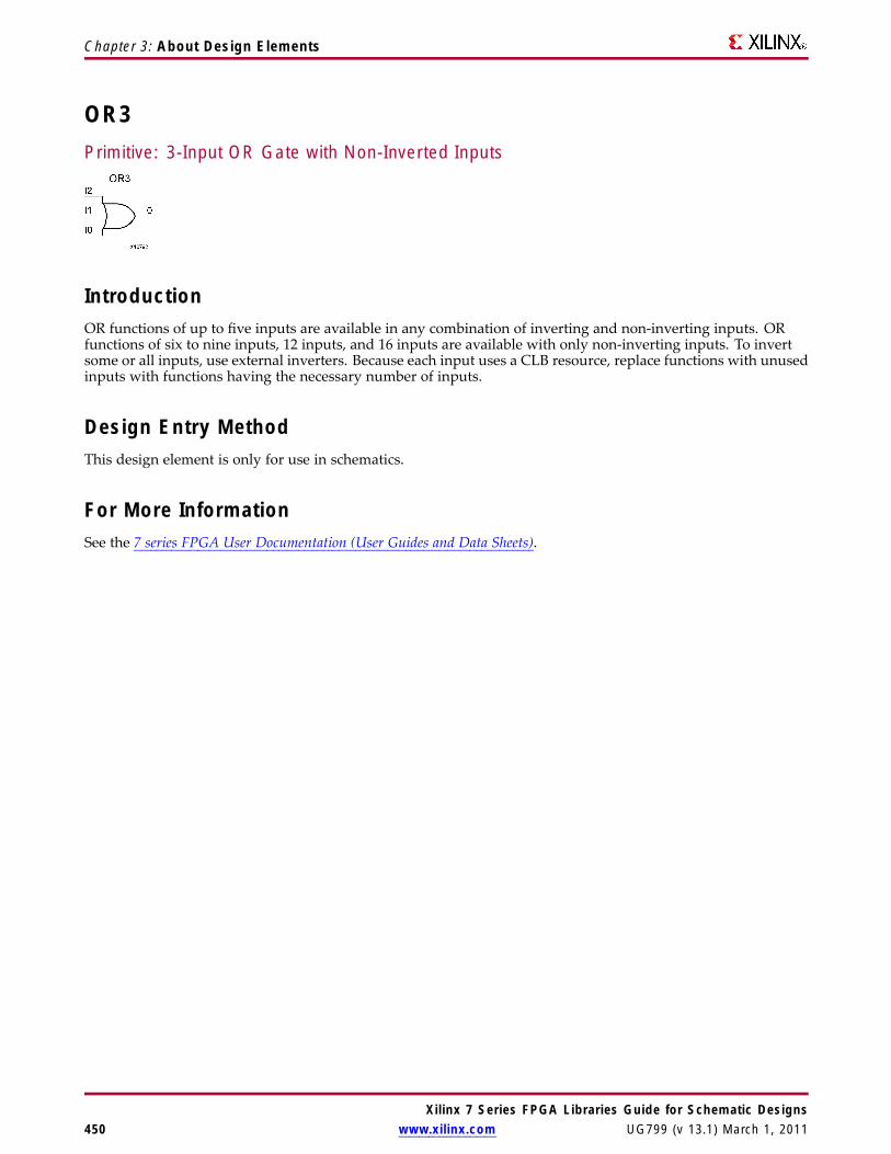
Chapter 3: About Design Elements
OR3Primitive: 3-Input OR Gate with Non-Inverted Inputs
IntroductionOR functions of up to five inputs are available in any combination of inverting and non-inverting inputs. ORfunctions of six to nine inputs, 12 inputs, and 16 inputs are available with only non-inverting inputs. To invertsome or all inputs, use external inverters. Because each input uses a CLB resource, replace functions with unusedinputs with functions having the necessary number of inputs.
Design Entry MethodThis design element is only for use in schematics.
For More InformationSee the 7 series FPGA User Documentation (User Guides and Data Sheets).
Xilinx 7 Series FPGA Libraries Guide for Schematic Designs450 www.xilinx.com UG799 (v 13.1) March 1, 2011

Chapter 3: About Design Elements
OR3B1Primitive: 3-Input OR Gate with 1 Inverted and 2 Non-Inverted Inputs
IntroductionOR functions of up to five inputs are available in any combination of inverting and non-inverting inputs. ORfunctions of six to nine inputs, 12 inputs, and 16 inputs are available with only non-inverting inputs. To invertsome or all inputs, use external inverters. Because each input uses a CLB resource, replace functions with unusedinputs with functions having the necessary number of inputs.
Design Entry MethodThis design element is only for use in schematics.
For More InformationSee the 7 series FPGA User Documentation (User Guides and Data Sheets).
Xilinx 7 Series FPGA Libraries Guide for Schematic DesignsUG799 (v 13.1) March 1, 2011 www.xilinx.com 451

Chapter 3: About Design Elements
OR3B2Primitive: 3-Input OR Gate with 2 Inverted and 1 Non-Inverted Inputs
IntroductionOR functions of up to five inputs are available in any combination of inverting and non-inverting inputs. ORfunctions of six to nine inputs, 12 inputs, and 16 inputs are available with only non-inverting inputs. To invertsome or all inputs, use external inverters. Because each input uses a CLB resource, replace functions with unusedinputs with functions having the necessary number of inputs.
Design Entry MethodThis design element is only for use in schematics.
For More InformationSee the 7 series FPGA User Documentation (User Guides and Data Sheets).
Xilinx 7 Series FPGA Libraries Guide for Schematic Designs452 www.xilinx.com UG799 (v 13.1) March 1, 2011

Chapter 3: About Design Elements
OR3B3Primitive: 3-Input OR Gate with Inverted Inputs
IntroductionOR functions of up to five inputs are available in any combination of inverting and non-inverting inputs. ORfunctions of six to nine inputs, 12 inputs, and 16 inputs are available with only non-inverting inputs. To invertsome or all inputs, use external inverters. Because each input uses a CLB resource, replace functions with unusedinputs with functions having the necessary number of inputs.
Design Entry MethodThis design element is only for use in schematics.
For More InformationSee the 7 series FPGA User Documentation (User Guides and Data Sheets).
Xilinx 7 Series FPGA Libraries Guide for Schematic DesignsUG799 (v 13.1) March 1, 2011 www.xilinx.com 453

Chapter 3: About Design Elements
OR4Primitive: 4-Input OR Gate with Non-Inverted Inputs
IntroductionOR functions of up to five inputs are available in any combination of inverting and non-inverting inputs. ORfunctions of six to nine inputs, 12 inputs, and 16 inputs are available with only non-inverting inputs. To invertsome or all inputs, use external inverters. Because each input uses a CLB resource, replace functions with unusedinputs with functions having the necessary number of inputs.
Design Entry MethodThis design element is only for use in schematics.
For More InformationSee the 7 series FPGA User Documentation (User Guides and Data Sheets).
Xilinx 7 Series FPGA Libraries Guide for Schematic Designs454 www.xilinx.com UG799 (v 13.1) March 1, 2011

Chapter 3: About Design Elements
OR4B1Primitive: 4-Input OR Gate with 1 Inverted and 3 Non-Inverted Inputs
IntroductionOR functions of up to five inputs are available in any combination of inverting and non-inverting inputs. ORfunctions of six to nine inputs, 12 inputs, and 16 inputs are available with only non-inverting inputs. To invertsome or all inputs, use external inverters. Because each input uses a CLB resource, replace functions with unusedinputs with functions having the necessary number of inputs.
Design Entry MethodThis design element is only for use in schematics.
For More InformationSee the 7 series FPGA User Documentation (User Guides and Data Sheets).
Xilinx 7 Series FPGA Libraries Guide for Schematic DesignsUG799 (v 13.1) March 1, 2011 www.xilinx.com 455

Chapter 3: About Design Elements
OR4B2Primitive: 4-Input OR Gate with 2 Inverted and 2 Non-Inverted Inputs
IntroductionOR functions of up to five inputs are available in any combination of inverting and non-inverting inputs. ORfunctions of six to nine inputs, 12 inputs, and 16 inputs are available with only non-inverting inputs. To invertsome or all inputs, use external inverters. Because each input uses a CLB resource, replace functions with unusedinputs with functions having the necessary number of inputs.
Design Entry MethodThis design element is only for use in schematics.
For More InformationSee the 7 series FPGA User Documentation (User Guides and Data Sheets).
Xilinx 7 Series FPGA Libraries Guide for Schematic Designs456 www.xilinx.com UG799 (v 13.1) March 1, 2011

Chapter 3: About Design Elements
OR4B3Primitive: 4-Input OR Gate with 3 Inverted and 1 Non-Inverted Inputs
IntroductionOR functions of up to five inputs are available in any combination of inverting and non-inverting inputs. ORfunctions of six to nine inputs, 12 inputs, and 16 inputs are available with only non-inverting inputs. To invertsome or all inputs, use external inverters. Because each input uses a CLB resource, replace functions with unusedinputs with functions having the necessary number of inputs.
Design Entry MethodThis design element is only for use in schematics.
For More InformationSee the 7 series FPGA User Documentation (User Guides and Data Sheets).
Xilinx 7 Series FPGA Libraries Guide for Schematic DesignsUG799 (v 13.1) March 1, 2011 www.xilinx.com 457

Chapter 3: About Design Elements
OR4B4Primitive: 4-Input OR Gate with Inverted Inputs
IntroductionOR functions of up to five inputs are available in any combination of inverting and non-inverting inputs. ORfunctions of six to nine inputs, 12 inputs, and 16 inputs are available with only non-inverting inputs. To invertsome or all inputs, use external inverters. Because each input uses a CLB resource, replace functions with unusedinputs with functions having the necessary number of inputs.
Design Entry MethodThis design element is only for use in schematics.
For More InformationSee the 7 series FPGA User Documentation (User Guides and Data Sheets).
Xilinx 7 Series FPGA Libraries Guide for Schematic Designs458 www.xilinx.com UG799 (v 13.1) March 1, 2011

Chapter 3: About Design Elements
OR5Primitive: 5-Input OR Gate with Non-Inverted Inputs
IntroductionOR functions of up to five inputs are available in any combination of inverting and non-inverting inputs. ORfunctions of six to nine inputs, 12 inputs, and 16 inputs are available with only non-inverting inputs. To invertsome or all inputs, use external inverters. Because each input uses a CLB resource, replace functions with unusedinputs with functions having the necessary number of inputs.
Design Entry MethodThis design element is only for use in schematics.
For More InformationSee the 7 series FPGA User Documentation (User Guides and Data Sheets).
Xilinx 7 Series FPGA Libraries Guide for Schematic DesignsUG799 (v 13.1) March 1, 2011 www.xilinx.com 459

Chapter 3: About Design Elements
OR5B1Primitive: 5-Input OR Gate with 1 Inverted and 4 Non-Inverted Inputs
IntroductionOR functions of up to five inputs are available in any combination of inverting and non-inverting inputs. ORfunctions of six to nine inputs, 12 inputs, and 16 inputs are available with only non-inverting inputs. To invertsome or all inputs, use external inverters. Because each input uses a CLB resource, replace functions with unusedinputs with functions having the necessary number of inputs.
Design Entry MethodThis design element is only for use in schematics.
For More InformationSee the 7 series FPGA User Documentation (User Guides and Data Sheets).
Xilinx 7 Series FPGA Libraries Guide for Schematic Designs460 www.xilinx.com UG799 (v 13.1) March 1, 2011

Chapter 3: About Design Elements
OR5B2Primitive: 5-Input OR Gate with 2 Inverted and 3 Non-Inverted Inputs
IntroductionOR functions of up to five inputs are available in any combination of inverting and non-inverting inputs. ORfunctions of six to nine inputs, 12 inputs, and 16 inputs are available with only non-inverting inputs. To invertsome or all inputs, use external inverters. Because each input uses a CLB resource, replace functions with unusedinputs with functions having the necessary number of inputs.
Design Entry MethodThis design element is only for use in schematics.
For More InformationSee the 7 series FPGA User Documentation (User Guides and Data Sheets).
Xilinx 7 Series FPGA Libraries Guide for Schematic DesignsUG799 (v 13.1) March 1, 2011 www.xilinx.com 461

Chapter 3: About Design Elements
OR5B3Primitive: 5-Input OR Gate with 3 Inverted and 2 Non-Inverted Inputs
IntroductionOR functions of up to five inputs are available in any combination of inverting and non-inverting inputs. ORfunctions of six to nine inputs, 12 inputs, and 16 inputs are available with only non-inverting inputs. To invertsome or all inputs, use external inverters. Because each input uses a CLB resource, replace functions with unusedinputs with functions having the necessary number of inputs.
Design Entry MethodThis design element is only for use in schematics.
For More InformationSee the 7 series FPGA User Documentation (User Guides and Data Sheets).
Xilinx 7 Series FPGA Libraries Guide for Schematic Designs462 www.xilinx.com UG799 (v 13.1) March 1, 2011

Chapter 3: About Design Elements
OR5B4Primitive: 5-Input OR Gate with 4 Inverted and 1 Non-Inverted Inputs
IntroductionOR functions of up to five inputs are available in any combination of inverting and non-inverting inputs. ORfunctions of six to nine inputs, 12 inputs, and 16 inputs are available with only non-inverting inputs. To invertsome or all inputs, use external inverters. Because each input uses a CLB resource, replace functions with unusedinputs with functions having the necessary number of inputs.
Design Entry MethodThis design element is only for use in schematics.
For More InformationSee the 7 series FPGA User Documentation (User Guides and Data Sheets).
Xilinx 7 Series FPGA Libraries Guide for Schematic DesignsUG799 (v 13.1) March 1, 2011 www.xilinx.com 463

Chapter 3: About Design Elements
OR5B5Primitive: 5-Input OR Gate with Inverted Inputs
IntroductionOR functions of up to five inputs are available in any combination of inverting and non-inverting inputs. ORfunctions of six to nine inputs, 12 inputs, and 16 inputs are available with only non-inverting inputs. To invertsome or all inputs, use external inverters. Because each input uses a CLB resource, replace functions with unusedinputs with functions having the necessary number of inputs.
Design Entry MethodThis design element is only for use in schematics.
For More InformationSee the 7 series FPGA User Documentation (User Guides and Data Sheets).
Xilinx 7 Series FPGA Libraries Guide for Schematic Designs464 www.xilinx.com UG799 (v 13.1) March 1, 2011
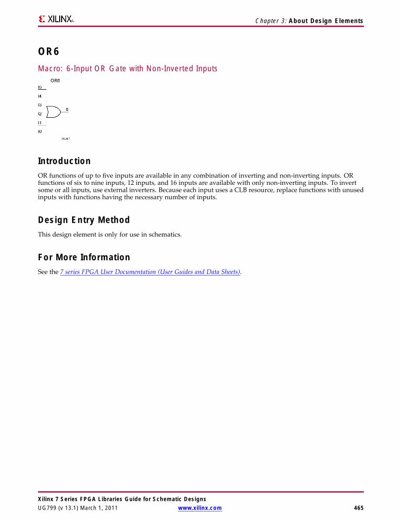
Chapter 3: About Design Elements
OR6Macro: 6-Input OR Gate with Non-Inverted Inputs
IntroductionOR functions of up to five inputs are available in any combination of inverting and non-inverting inputs. ORfunctions of six to nine inputs, 12 inputs, and 16 inputs are available with only non-inverting inputs. To invertsome or all inputs, use external inverters. Because each input uses a CLB resource, replace functions with unusedinputs with functions having the necessary number of inputs.
Design Entry MethodThis design element is only for use in schematics.
For More InformationSee the 7 series FPGA User Documentation (User Guides and Data Sheets).
Xilinx 7 Series FPGA Libraries Guide for Schematic DesignsUG799 (v 13.1) March 1, 2011 www.xilinx.com 465

Chapter 3: About Design Elements
OR7Macro: 7-Input OR Gate with Non-Inverted Inputs
IntroductionOR functions of up to five inputs are available in any combination of inverting and non-inverting inputs. ORfunctions of six to nine inputs, 12 inputs, and 16 inputs are available with only non-inverting inputs. To invertsome or all inputs, use external inverters. Because each input uses a CLB resource, replace functions with unusedinputs with functions having the necessary number of inputs.
Design Entry MethodThis design element is only for use in schematics.
For More InformationSee the 7 series FPGA User Documentation (User Guides and Data Sheets).
Xilinx 7 Series FPGA Libraries Guide for Schematic Designs466 www.xilinx.com UG799 (v 13.1) March 1, 2011

Chapter 3: About Design Elements
OR8Macro: 8-Input OR Gate with Non-Inverted Inputs
IntroductionOR functions of up to five inputs are available in any combination of inverting and non-inverting inputs. ORfunctions of six to nine inputs, 12 inputs, and 16 inputs are available with only non-inverting inputs. To invertsome or all inputs, use external inverters. Because each input uses a CLB resource, replace functions with unusedinputs with functions having the necessary number of inputs.
Design Entry MethodThis design element is only for use in schematics.
For More InformationSee the 7 series FPGA User Documentation (User Guides and Data Sheets).
Xilinx 7 Series FPGA Libraries Guide for Schematic DesignsUG799 (v 13.1) March 1, 2011 www.xilinx.com 467

Chapter 3: About Design Elements
OR9Macro: 9-Input OR Gate with Non-Inverted Inputs
IntroductionOR functions of up to five inputs are available in any combination of inverting and non-inverting inputs. ORfunctions of six to nine inputs, 12 inputs, and 16 inputs are available with only non-inverting inputs. To invertsome or all inputs, use external inverters. Because each input uses a CLB resource, replace functions with unusedinputs with functions having the necessary number of inputs.
Design Entry MethodThis design element is only for use in schematics.
For More InformationSee the 7 series FPGA User Documentation (User Guides and Data Sheets).
Xilinx 7 Series FPGA Libraries Guide for Schematic Designs468 www.xilinx.com UG799 (v 13.1) March 1, 2011
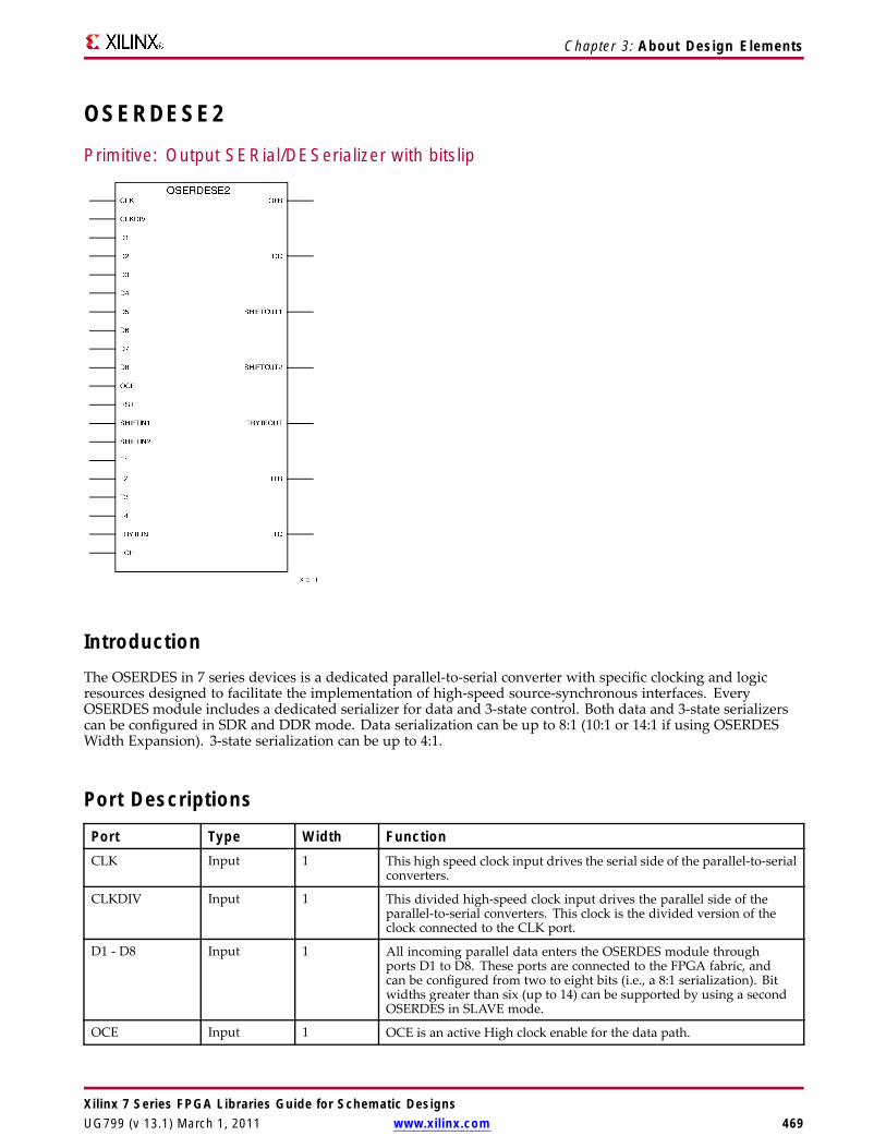
Chapter 3: About Design Elements
OSERDESE2Primitive: Output SERial/DESerializer with bitslip
IntroductionThe OSERDES in 7 series devices is a dedicated parallel-to-serial converter with specific clocking and logicresources designed to facilitate the implementation of high-speed source-synchronous interfaces. EveryOSERDES module includes a dedicated serializer for data and 3-state control. Both data and 3-state serializerscan be configured in SDR and DDR mode. Data serialization can be up to 8:1 (10:1 or 14:1 if using OSERDESWidth Expansion). 3-state serialization can be up to 4:1.
Port Descriptions
Port Type Width FunctionCLK Input 1 This high speed clock input drives the serial side of the parallel-to-serial
converters.
CLKDIV Input 1 This divided high-speed clock input drives the parallel side of theparallel-to-serial converters. This clock is the divided version of theclock connected to the CLK port.
D1 - D8 Input 1 All incoming parallel data enters the OSERDES module throughports D1 to D8. These ports are connected to the FPGA fabric, andcan be configured from two to eight bits (i.e., a 8:1 serialization). Bitwidths greater than six (up to 14) can be supported by using a secondOSERDES in SLAVE mode.
OCE Input 1 OCE is an active High clock enable for the data path.
Xilinx 7 Series FPGA Libraries Guide for Schematic DesignsUG799 (v 13.1) March 1, 2011 www.xilinx.com 469

Chapter 3: About Design Elements
Port Type Width FunctionOFB Output 1 The output feedback port (OFB) is the serial (high-speed) data output
port of the OSERDESE2.
OQ Output 1 The OQ port is the data output port of the OSERDES module. Data atthe input port D1 will appear first at OQ. This port connects the outputof the data parallel-to-serial converter to the data input of the IOB. Thisport can not drive the ODELAYE2; the OFB pin must be used.
RST Input 1 The reset input causes the outputs of all data flip-flops in the CLK andCLKDIV domains to be driven Low asynchronously. OSERDES circuitsrunning in the CLK domain where timing is critical use an internal,dedicated circuit to retime the RST input to produce a reset signalsynchronous to the CLK domain. Similarly, there is a dedicated circuitto retime the RST input to produce a reset signal synchronous to theCLKDIV domain. Because there are OSERDES circuits that retimethe RST input, the user is only required to provide a reset pulse tothe RST input that meets timing on the CLKDIV frequency domain(synchronous to CLKDIV). Therefore, RST should be driven High for aminimum of one CLKDIV cycle. When building an interface consistingof multiple OSERDES ports, all OSERDES ports must be synchronized.The internal retiming of the RST input is designed so that all OSERDESblocks that receive the same reset pulse come out of reset synchronizedwith one another.
SHIFTIN1 /SHIFTIN2
Input 1 Cascade Input for data input expansion. Connect to SHIFTOUT1 / 2of slave.
SHIFTOUT1 /SHIFTOUT2
Output 1 Cascade out for data input expansion. Connect to SHIFTIN1 / 2 ofmaster.
TBYTEIN Input 1 Byte group tristate input from source .
TBYTEOUT Output 1 Byte group tristate output to IOB .
TCE Input 1 TCE is an active High clock enable for the 3-state control path.
TFB Output 1 This port is the 3-state control output of the OSERDES module sentto the ODELAYE2. When used, this port connects the output of the3-state parallel-to-serial converter to the control/3-state input of theODELAYE2.
TQ Output 1 This port is the 3-state control output of the OSERDES module. Whenused, this port connects the output of the 3-state parallel-to-serialconverter to the control/3-state input of the IOB.
T1 - T4 Input 1 All parallel 3-state signals enter the OSERDES module through portsT1 to T4. The ports are connected to the FPGA fabric, and can beconfigured as one, two, or four bits.
Design Entry MethodThis design element can be used in schematics.
Available AttributesAttribute Type Allowed Values Default DescriptionDATA_RATE_OQ STRING DDR, SDR DDR The DATA_RATE_OQ attribute defines
whether data is processed as singledata rate (SDR) or double data rate(DDR).
Xilinx 7 Series FPGA Libraries Guide for Schematic Designs470 www.xilinx.com UG799 (v 13.1) March 1, 2011

Chapter 3: About Design Elements
Attribute Type Allowed Values Default DescriptionDATA_RATE_TQ STRING DDR, BUF, SDR DDR The DATA_RATE_TQ attribute defines
whether 3-state control is to beprocessed as single data rate (SDR) ordouble data rate (DDR).
DATA_WIDTH DECIMAL 4, 2, 3, 5, 6, 7, 8, 10, 14 4 The DATA_WIDTH attribute definesthe parallel data input width ofthe parallel-to-serial converter. Thepossible values for this attributedepend on the DATA_RATE_OQattribute. When DATA_RATE_OQ isset to SDR, the possible values for theDATA_WIDTH attribute are 2, 3, 4, 5,6, 7, and 8. When DATA_RATE_OQis set to DDR, the possible values forthe DATA_WIDTH attribute are 4, 6, 8,10 and 14. When the DATA_WIDTH isset to widths larger than eight, a pairof OSERDES must be configured into amaster-slave configuration.
INIT_OQ BINARY 1’b0 to 1’b1 1’b0 Defines the initial value of OQ output.
INIT_TQ BINARY 1’b0 to 1’b1 1’b0 Defines the initial value of TQ output.
SERDES_MODE STRING MASTER, SLAVE MASTER The SERDES_MODE attribute defineswhether the OSERDES module is amaster or slave when using widthexpansion.
SRVAL_OQ BINARY 1’b0 to 1’b1 1’b0 Defines the value of OQ outputs whenthe SR is invoked.
SRVAL_TQ BINARY 1’b0 to 1’b1 1’b0 Defines the value of YQ outputs whenthe SR is invoked.
TBYTE_CTL STRING FALSE, TRUE FALSE Enable Tristate BYTE operation forDDR3 mode. This allows the tristatesignal to take value from one of thetristate outputs which is acting as asource.
TBYTE_SRC STRING FALSE, TRUE FALSE Enable OSERDES to act as a source forTristate Byte operation in DDR3 mode.
TRISTATE_WIDTH
DECIMAL 4, 1 4 The TRISTATE_WIDTH attributedefines the parallel 3-state input widthof the 3-state control parallel-to-serialconverter. The possible valuesfor this attribute depend on theDATA_RATE_TQ attribute. WhenDATA_RATE_TQ is set to SDRor BUF, the TRISTATE_WIDTHattribute can only be set to 1.When DATA_RATE_TQ is set toDDR, the possible values for theTRISTATE_WIDTH attribute is 4.TRISTATE_WIDTH cannot be setto widths larger than 4. When aDATA_WIDTH is larger than four, setthe TRISTATE_WIDTH to 1.
Xilinx 7 Series FPGA Libraries Guide for Schematic DesignsUG799 (v 13.1) March 1, 2011 www.xilinx.com 471

Chapter 3: About Design Elements
For More Information• See the 7 series FPGA SelectIO Resources User Guide.
• See the 7 series FPGA Data Sheet DC and Switching Characteristics.
Xilinx 7 Series FPGA Libraries Guide for Schematic Designs472 www.xilinx.com UG799 (v 13.1) March 1, 2011

Chapter 3: About Design Elements
PLLE2_ADVPrimitive: Phase Locked Loop
IntroductionThe PLLE2 is a mixed signal block designed to support frequency synthesis, clock network deskew, and jitterreduction. The clock outputs can each have an individual divide, phase shift and duty cycle based on the sameVCO frequency. The PLLE2 compliments the MMCM by supporting higher speed clocking while the MMCMhas more features to handle most general clocking needs. The PLLE2_BASE is intended for most uses of thisPLL component while the PLLE2_ADV is intended for use when clock switch-over or dynamic reconfigurationis required.
Port DescriptionsPort Type Width FunctionCLKFBIN Input 1 Feedback clock pin to the PLL
CLKFBOUT Output 1 Dedicated PLL Feedback clock output
CLKINSEL Input 1 Signal controls the state of the input MUX, High = CLKIN1, Low =CLKIN2.
CLKIN1 Input 1 Primary clock input.
CLKIN2 Input 1 Secondary clock input.
CLKOUT0 Output 1 CLKOUT0 output
CLKOUT1 Output 1 CLKOUT1 output
CLKOUT2 Output 1 CLKOUT2 output
CLKOUT3 Output 1 CLKOUT3 output
CLKOUT4 Output 1 CLKOUT4 output
CLKOUT5 Output 1 CLKOUT5 output
DADDR<6:0> Input 7 The dynamic reconfiguration address (DADDR) input bus provides areconfiguration address for the dynamic reconfiguration. When notused, all bits must be assigned zeros.
DCLK Input 1 The DCLK signal is the reference clock for the dynamic reconfigurationport.
DEN Input 1 The dynamic reconfiguration enable (DEN) provides the enable controlsignal to access the dynamic reconfiguration feature. When the dynamicreconfiguration feature is not used, DEN must be tied Low.
Xilinx 7 Series FPGA Libraries Guide for Schematic DesignsUG799 (v 13.1) March 1, 2011 www.xilinx.com 473

Chapter 3: About Design Elements
Port Type Width FunctionDI<15:0> Input 16 The dynamic reconfiguration data input (DI) bus provides
reconfiguration data. When not used, all bits must be set to zero.
DO<15:0> Output 16 The dynamic reconfiguration output bus provides PLL data outputwhen using dynamic reconfiguration.
DRDY Output 1 The dynamic reconfiguration ready output (DRDY) provides theresponse to the DEN signal for the PLLs dynamic reconfigurationfeature.
DWE Input 1 The dynamic reconfiguration write enable (DWE) input pin providesthe write enable control signal to write the DI data into the DADDRaddress. When not used, it must be tied Low.
LOCKED Output 1 An output from the PLL that indicates when the PLL has achieved phasealignment within a predefined window and frequency matching withina predefined PPM range. The PLL automatically locks after power on,no extra reset is required. LOCKED will be deasserted if the input clockstops or the phase alignment is violated (e.g., input clock phase shift).The PLL automatically reacquires lock after LOCKED is deasserted.
PWRDWN Input 1 Powers down instantiated but unused PLLs.
RST Input 1 Asynchronous reset signal. The RST signal is an asynchronous reset forthe PLL. The PLL will synchronously re-enable itself when this signal isreleased and go through a new phase alignment and lock cycle. A resetis not required when the input clock conditions change (e.g., frequency).
Status Ports Output 1 An output from the PLL that indicates when the PLL has achieved phasealignment within a predefined window and frequency matching withina predefined PPM range. The PLL automatically locks after power on,no extra reset is required. LOCKED will be deasserted if the input clockstops or the phase alignment is violated (e.g., input clock phase shift).The PLL automatically reacquires lock after LOCKED is deasserted.
Design Entry MethodThis design element can be used in schematics.
Available AttributesAttribute Type Allowed Values Default DescriptionBANDWIDTH STRING OPTIMIZED, HIGH,
LOWOPTIMIZED Specifies the PLLE2 programming
algorithm affecting the jitter, phasemargin and other characteristics of thePLLE2.
CLKFBOUT_MULT
DECIMAL 2 to 64 5 Specifies the amount to multiplyall CLKOUT clock outputs if adifferent frequency is desired. Thisnumber, in combination with theassociated CLKOUT#_DIVIDE valueand DIVCLK_DIVIDE value, will
CLKFBOUT_PHASE
3 significantdigit FLOAT
-360.000 to 360.000 0.000 Specifies the phase offset in degreesof the clock feedback output. Shiftingthe feedback clock results in a negativephase shift of all output clocks to thePLL.
Xilinx 7 Series FPGA Libraries Guide for Schematic Designs474 www.xilinx.com UG799 (v 13.1) March 1, 2011
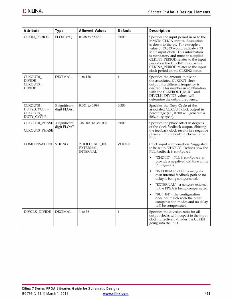
Chapter 3: About Design Elements
Attribute Type Allowed Values Default DescriptionCLKIN_PERIOD FLOAT(nS) 0.938 to 52.631 0.000 Specifies the input period in ns to the
MMCM CLKIN inputs. Resolutionis down to the ps. For exmaple avalue of 33.333 would indicate a 33MHz input clock. This informationis mandatory and must be supplied.CLKIN1_PERIOD relates to the inputperiod on the CLKIN1 input whileCLKIN2_PERIOD relates to the inputclock period on the CLKIN2 input.
CLKOUT0_DIVIDE -CLKOUT5_DIVIDE
DECIMAL 1 to 128 1 Specifies the amount to dividethe associated CLKOUT clockoutput if a different frequency isdesired. This number in combinationwith the CLKFBOUT_MULT andDIVCLK_DIVIDE values willdetermine the output frequency.
CLKOUT0_DUTY_CYCLE -CLKOUT5_DUTY_CYCLE
3 significantdigit FLOAT
0.001 to 0.999 0.500 Specifies the Duty Cycle of theassociated CLKOUT clock output inpercentage (i.e., 0.500 will generate a50% duty cycle).
CLKOUT0_PHASE-CLKOUT5_PHASE
3 significantdigit FLOAT
-360.000 to 360.000 0.000 Specifies the phase offset in degreesof the clock feedback output. Shiftingthe feedback clock results in a negativephase shift of all output clocks to thePLL.
COMPENSATION STRING ZHOLD, BUF_IN,EXTERNAL,INTERNAL
ZHOLD Clock input compensation. Suggestedto be set to "ZHOLD". Defines how thePLL feedback is configured.
• "ZHOLD" - PLL is configured toprovide a negative hold time at theI/O registers.
• "INTERNAL" - PLL is using itsown internal feedback path so nodelay is being compensated.
• "EXTERNAL" - a network externalto the FPGA is being compensated.
• "BUF_IN" - the configurationdoes not match with the othercompensation modes and no delaywill be compensated.
DIVCLK_DIVIDE DECIMAL 1 to 56 1 Specifies the division ratio for alloutput clocks with respect to the inputclock. Effectively divides the CLKINgoing into the PFD.
Xilinx 7 Series FPGA Libraries Guide for Schematic DesignsUG799 (v 13.1) March 1, 2011 www.xilinx.com 475

Chapter 3: About Design Elements
Attribute Type Allowed Values Default DescriptionREF_JITTER 3 significant
digit FLOAT0.000 to 0.999 0.010 Allows specification of the expected
jitter on the CLKIN inputs in order tobetter optimize PLL performance. Abandwidth setting of OPTIMIZED willattempt to choose the best parameterfor input clocking when unknown.If known, then the value providedshould be specified in terms of the UIpercentage (the maximum peak to peakvalue) of the expected jitter on the inputclock. REF_JITTER1 relates to the inputjitter on CLKIN1 while REF_JITTER2relates to the input jitter on CLKIN2.
STARTUP_WAIT STRING FALSE, TRUE FALSE When TRUE, wait for the PLLE2(s) thathave this attribute attached to themwill delay DONE from going high untila LOCK is achieved.
For More Information• See the 7 series FPGA SelectIO Resources User Guide.
• See the 7 series FPGA Data Sheet DC and Switching Characteristics.
Xilinx 7 Series FPGA Libraries Guide for Schematic Designs476 www.xilinx.com UG799 (v 13.1) March 1, 2011

Chapter 3: About Design Elements
PLLE2_BASEPrimitive: Basic Phase Locked Loop Clock Circuit
IntroductionThe PLLE2 is a mixed signal block designed to support frequency synthesis, clock network deskew, and jitterreduction. The clock outputs can each have an individual divide, phase shift, and duty cycle based on the sameVCO frequency. The PLLE2 compliments the MMCM by supporting higher speed clocking while the MMCMhas more features to handle most general clocking needs. The PLLE2_BASE is intended for most uses of thisPLL component while the PLLE2_ADV is intended for use when clock switch-over or dynamic reconfigurationis required.
Port DescriptionsPort Direction Width Function
Clock Outputs/Inputs
CLKOUT0-5 Output 1 User configurable clock outputs that can bedivided versions of the VCO phase outputs (usercontrollable) from 1 (bypassed) to 128. The outputclocks are phase aligned to each other (unless phaseshifted) and aligned to the input clock with a properfeedback configuration.
CLKFBOUT Output 1 Dedicated PLL Feedback clock output. Requiredports to form the feedback path for the PLL phasealignment capabilities.
CLKIN Input 1 Clock source input to the PLL. This pin can bedriven by a dedicated clock pin to the FPGA, a DCMoutput clock pin, or a BUFG output.
CLKFBIN Input 1 Feedback clock pin to the PLL. Required ports toform the feedback path for the PLL phase alignmentcapabilities.
Status Outputs/Control Inputs
LOCKED Output 1 An output from the PLL that indicates whenthe PLL has achieved phase alignment within apredefined window and frequency matching withina predefined PPM range. The PLL automaticallylocks after power on, no extra reset is required.LOCKED will be deasserted if the input clock stopsor the phase alignment is violated (e.g., input clock
Xilinx 7 Series FPGA Libraries Guide for Schematic DesignsUG799 (v 13.1) March 1, 2011 www.xilinx.com 477

Chapter 3: About Design Elements
Port Direction Width Functionphase shift). The PLL automatically reacquires lockafter LOCKED is deasserted.
PWRDWN Input 1 Powers down instantiated but unused PLLs. PLLcontrol ports.
RST Input 1 Asynchronous reset signal. The RST signal isan asynchronous reset for the PLL. The PLL willsynchronously re-enable itself when this signal isreleased and go through a new phase alignmentand lock cycle. A reset is not required when theinput clock conditions change (e.g., frequency). PLLcontrol ports.
Design Entry MethodThis design element can be used in schematics.
Available AttributesAttribute Type Allowed Values Default DescriptionBANDWIDTH String "HIGH", "LOW",
"OPTIMIZED""OPTIMIZED" Specifies the PLL programming
algorithm affecting the jitter, phasemargin and other characteristics of thePLL.
CLKOUT0_DIVIDE,CLKOUT1_DIVIDE,CLKOUT2_DIVIDE,CLKOUT3_DIVIDE,CLKOUT4_DIVIDE,CLKOUT5_DIVIDE
Integer 1 to 128 1 Specifies the phase offset in degreesof the clock feedback output. Shiftingthe feedback clock results in a negativephase shift of all output clocks to thePLL.
CLKOUT0_PHASE,CLKOUT1_PHASE,CLKOUT2_PHASE,CLKOUT3_PHASE,CLKOUT4_PHASE,CLKOUT5_PHASE
Real 0.01 to 360.0 0.0 Allows specification of the outputphase relationship of the associatedCLKOUT clock output in number ofdegrees offset (i.e. 90 indicates a 90degree or ¼ cycle offset phase offsetwhile 180 indicates a 180 degree offsetor ½ cycle phase offset).
CLKOUT0_DUTY_CYCLE,CLKOUT1_DUTY_CYCLE,CLKOUT2_DUTY_CYCLE,CLKOUT3_DUTY_CYCLE,CLKOUT4_DUTY_CYCLE,CLKOUT5_DUTY_CYCLE,
Real 0.01 to 0.99 0.50 Specifies the Duty Cycle of theassociated CLKOUT clock output inpercentage (i.e. 0.50 generates a 50%duty cycle).
Xilinx 7 Series FPGA Libraries Guide for Schematic Designs478 www.xilinx.com UG799 (v 13.1) March 1, 2011

Chapter 3: About Design Elements
Attribute Type Allowed Values Default DescriptionCLKFBOUT_MULT Integer 1 to 64 1 Specifies the amount to multiply all
CLKOUT clock outputs if a differentfrequency is desired. This numberin combination with the associatedCLKOUT#_DIVIDE value determinesthe output frequency.
DIVCLK_DIVIDE Integer 1 to 52 1 Specifies the division ratio for alloutput clocks with respect to the inputclock. Effectively divides the CLKINgoing into the PFD.
CLKFBOUT_PHASE Real 0.0 to 360 0.0 Specifies the phase offset in degrees ofthe clock feedback output.
REF_JITTER1 Real 0.000 to 0.999 0.100 Allows specification of the expectedjitter on CLKIN1 in order to betteroptimize PLL performance. Abandwidth setting of OPTIMIZED willattempt to choose the best parameterfor input clocking when unknown.If known, then the value providedshould be specified in terms of theUI percentage (the maximum peak topeak value) of the expected jitter onthe input clock.
CLKIN1_PERIOD Real 1.000 to 52.630 0.000 Specifies the input period in ns tothe PLL CLKIN1 input. Resolutionis down to the ps (3 decimal places).For exmaple a value of 33.333 wouldindicate a 30 MHz input clock. Thisinformation is mandatory and must besupplied.
STARTUP_WAIT String “TRUE”, “FALSE” “FALSE” When "TRUE", wait for the PLLE2(s)that have this attribute attached tothem will delay DONE from goinghigh until a LOCK is achieved.
For More InformationSee the 7 series FPGA User Documentation (User Guides and Data Sheets).
Xilinx 7 Series FPGA Libraries Guide for Schematic DesignsUG799 (v 13.1) March 1, 2011 www.xilinx.com 479

Chapter 3: About Design Elements
PULLDOWNPrimitive: Resistor to GND for Input Pads, Open-Drain, and 3-State Outputs
IntroductionThis resistor element is connected to input, output, or bidirectional pads to guarantee a logic Low level fornodes that might float.
Port DescriptionsPort Direction Width FunctionO Output 1 Pulldown output (connect directly to top level port)
Design Entry MethodThis design element can be used in schematics.
This element can be connected to a net in the following locations on a top-level schematic file:
• A net connected to an input IO Marker.
• A net connected to both an output IO Marker and 3-statable IO element, such as an OBUFT.
For More InformationSee the 7 series FPGA User Documentation (User Guides and Data Sheets).
Xilinx 7 Series FPGA Libraries Guide for Schematic Designs480 www.xilinx.com UG799 (v 13.1) March 1, 2011

Chapter 3: About Design Elements
PULLUPPrimitive: Resistor to VCC for Input PADs, Open-Drain, and 3-State Outputs
IntroductionThis design element allows for an input, 3-state output or bi-directional port to be driven to a weak highvalue when not being driven by an internal or external source. This element establishes a High logic level foropen-drain elements and macros when all the drivers are off.
Port DescriptionsPort Direction Width FunctionO Output 1 Pullup output (connect directly to top level port)
Design Entry MethodThis design element can be used in schematics.
This element can be connected to a net in the following locations on a top-level schematic file:
• A net connected to an input IO Marker
• A net connected to both an output IO Marker and 3-statable IO element, such as an OBUFT.
For More InformationSee the 7 series FPGA User Documentation (User Guides and Data Sheets).
Xilinx 7 Series FPGA Libraries Guide for Schematic DesignsUG799 (v 13.1) March 1, 2011 www.xilinx.com 481

Chapter 3: About Design Elements
RAM128X1DPrimitive: 128-Deep by 1-Wide Dual Port Random Access Memory (Select RAM)
IntroductionThis design element is a 128-bit deep by 1-bit wide random access memory and has a read/write port that writesthe value on the D input data pin when the write enable (WE) is high to the location specified by the A addressbus. This happens shortly after the rising edge of the WCLK and that same value is reflected in the data outputSPO. When WE is low, an asynchronous read is initiated in which the contents of the memory location specifiedby the A address bus is output asynchronously to the SPO output. The read port can perform asynchronousread access of the memory by changing the value of the address bus DPRA, and by outputing that value to theDPO data output.
Port DescriptionsPort Direction Width FunctionSPO Output 1 Read/Write port data output addressed by A
DPO Output 1 Read port data output addressed by DPRA
D Input 1 Write data input addressed by A
A Input 7 Read/Write port address bus
DPRA Input 7 Read port address bus
WE Input 1 Write Enable
WCLK Input 1 Write clock (reads are asynchronous)
If instantiated, the following connections should be made to this component:
• Tie the WCLK input to the desired clock source, the D input to the data source to be stored and the DPOoutput to an FDCE D input or other appropriate data destination.
• Optionally, the SPO output can also be connected to the appropriate data destination or else left unconnected.
• The WE clock enable pin should be connected to the proper write enable source in the design.
• The 7-bit A bus should be connected to the source for the read/write addressing and the 7-bit DPRA busshould be connected to the appropriate read address connections.
• An optional INIT attribute consisting of a 128-bit Hexadecimal value can be specified to indicate the initialcontents of the RAM.
If left unspecified, the initial contents default to all zeros.
Design Entry MethodThis design element can be used in schematics.
Xilinx 7 Series FPGA Libraries Guide for Schematic Designs482 www.xilinx.com UG799 (v 13.1) March 1, 2011

Chapter 3: About Design Elements
Available AttributesAttribute Type Allowed Values Default DescriptionINIT Hexadecimal Any 128-Bit Value All zeros Specifies the initial contents of the
RAM.
For More InformationSee the 7 series FPGA User Documentation (User Guides and Data Sheets).
Xilinx 7 Series FPGA Libraries Guide for Schematic DesignsUG799 (v 13.1) March 1, 2011 www.xilinx.com 483

Chapter 3: About Design Elements
RAM16X1DPrimitive: 16-Deep by 1-Wide Static Dual Port Synchronous RAM
IntroductionThis element is a 16-word by 1-bit static dual port random access memory with synchronous write capability.The device has two address ports: the read address (DPRA3:DPRA0) and the write address (A3:A0). These twoaddress ports are asynchronous. The read address controls the location of the data driven out of the output pin(DPO), and the write address controls the destination of a valid write transaction. When the write enable (WE) isLow, transitions on the write clock (WCLK) are ignored and data stored in the RAM is not affected.
When WE is High, any positive transition on (WCLK) loads the data on the data input (D) into the word selectedby the 4-bit write address. For predictable performance, write address and data inputs must be stable before aLow-to-High (WCLK) transition. This RAM block assumes an active-High (WCLK). (WCLK) can be active-Highor active-Low. Any inverter placed on the (WCLK) input net is absorbed into the block.
The SPO output reflects the data in the memory cell addressed by A3:A0. The DPO output reflects the datain the memory cell addressed by DPRA3:DPRA0.
Note The write process is not affected by the address on the read address port.
You can use the INIT attribute to directly specify an initial value. The value must be a hexadecimal number, forexample, INIT=ABAC. If the INIT attribute is not specified, the RAM is initialized with all zeros.
Logic TableMode selection is shown in the following logic table:
Inputs Outputs
WE (mode) WCLK D SPO DPO0 (read) X X data_a data_d
1 (read) 0 X data_a data_d
1 (read) 1 X data_a data_d
1 (write) ↑ D D data_d
1 (read) ↓ X data_a data_d
data_a = word addressed by bits A3-A0
data_d = word addressed by bits DPRA3-DPRA0
Xilinx 7 Series FPGA Libraries Guide for Schematic Designs484 www.xilinx.com UG799 (v 13.1) March 1, 2011

Chapter 3: About Design Elements
Design Entry MethodThis design element can be used in schematics.
Available AttributesAttribute Type Allowed Values Default DescriptionINIT Hexadecimal Any 16-Bit Value All
zeros.Initializes RAMs, registers, and look-uptables.
For More InformationSee the 7 series FPGA User Documentation (User Guides and Data Sheets).
Xilinx 7 Series FPGA Libraries Guide for Schematic DesignsUG799 (v 13.1) March 1, 2011 www.xilinx.com 485

Chapter 3: About Design Elements
RAM16X1D_1Primitive: 16-Deep by 1-Wide Static Dual Port Synchronous RAM with Negative-EdgeClock
IntroductionThis is a 16-word by 1-bit static dual port random access memory with synchronous write capability andnegative-edge clock. The device has two separate address ports: the read address (DPRA3:DPRA0) and the writeaddress (A3:A0). These two address ports are asynchronous. The read address controls the location of the datadriven out of the output pin (DPO), and the write address controls the destination of a valid write transaction.
When the write enable (WE) is set to Low, transitions on the write clock (WCLK) are ignored and data stored inthe RAM is not affected. When (WE) is High, any negative transition on (WCLK) loads the data on the datainput (D) into the word selected by the 4-bit write address. For predictable performance, write address anddata inputs must be stable before a High-to-Low WCLK transition. This RAM block assumes an active-High(WCLK). (WCLK) can be active-High or active-Low. Any inverter placed on the (WCLK) input net is absorbedinto the block.
You can initialize RAM16X1D_1 during configuration using the INIT attribute.
The SPO output reflects the data in the memory cell addressed by A3:A0. The DPO output reflects the datain the memory cell addressed by DPRA3:DPRA0.
Note The write process is not affected by the address on the read address port.
Logic TableMode selection is shown in the following logic table:
Inputs Outputs
WE (mode) WCLK D SPO DPO0 (read) X X data_a data_d
1 (read) 0 X data_a data_d
1 (read) 1 X data_a data_d
1 (write) ↓ D D data_d
1 (read) ↑ X data_a data_d
data_a = word addressed by bits A3:A0
data_d = word addressed by bits DPRA3:DPRA0
Xilinx 7 Series FPGA Libraries Guide for Schematic Designs486 www.xilinx.com UG799 (v 13.1) March 1, 2011
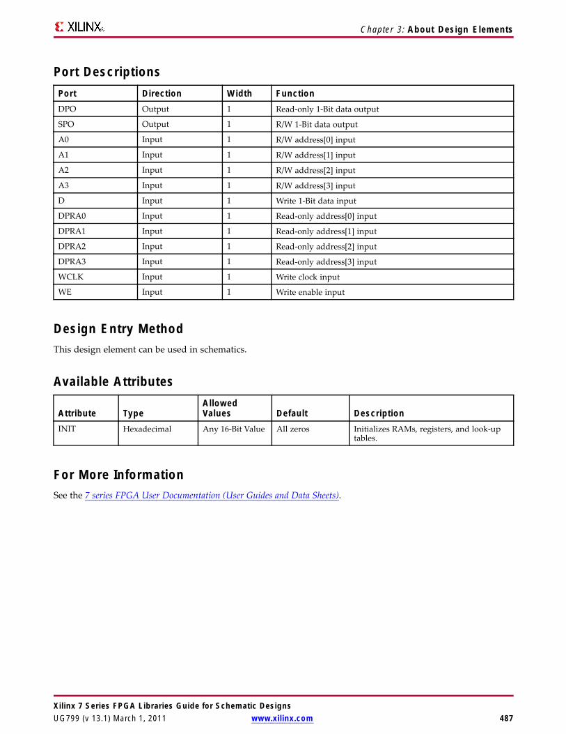
Chapter 3: About Design Elements
Port DescriptionsPort Direction Width FunctionDPO Output 1 Read-only 1-Bit data output
SPO Output 1 R/W 1-Bit data output
A0 Input 1 R/W address[0] input
A1 Input 1 R/W address[1] input
A2 Input 1 R/W address[2] input
A3 Input 1 R/W address[3] input
D Input 1 Write 1-Bit data input
DPRA0 Input 1 Read-only address[0] input
DPRA1 Input 1 Read-only address[1] input
DPRA2 Input 1 Read-only address[2] input
DPRA3 Input 1 Read-only address[3] input
WCLK Input 1 Write clock input
WE Input 1 Write enable input
Design Entry MethodThis design element can be used in schematics.
Available Attributes
Attribute TypeAllowedValues Default Description
INIT Hexadecimal Any 16-Bit Value All zeros Initializes RAMs, registers, and look-uptables.
For More InformationSee the 7 series FPGA User Documentation (User Guides and Data Sheets).
Xilinx 7 Series FPGA Libraries Guide for Schematic DesignsUG799 (v 13.1) March 1, 2011 www.xilinx.com 487

Chapter 3: About Design Elements
RAM16X1SPrimitive: 16-Deep by 1-Wide Static Synchronous RAM
IntroductionThis element is a 16-word by 1-bit static random access memory with synchronous write capability. When thewrite enable (WE) is set Low, transitions on the write clock (WCLK) are ignored and data stored in the RAM isnot affected. When WE is set High, any positive transition on WCLK loads the data on the data input (D) into theword selected by the 4-bit address (A3:A0). This RAM block assumes an active-High WCLK. However, WCLKcan be active-High or active-Low. Any inverter placed on the WCLK input net is absorbed into the block.
The signal output on the data output pin (O) is the data that is stored in the RAM at the location defined by thevalues on the address pins. You can initialize RAM16X1S during configuration using the INIT attribute.
Logic TableInputs Outputs
WE(mode) WCLK D O0 (read) X X Data
1 (read) 0 X Data
1 (read) 1 X Data
1 (write) ↑ D D
1 (read) ↓ X Data
Data = word addressed by bits A3:A0
Design Entry MethodThis design element can be used in schematics.
Available AttributesAttribute Type Allowed Values Default DescriptionINIT Hexadecimal Any 16-Bit Value All zeros Specifies initial contents of the
RAM.
For More InformationSee the 7 series FPGA User Documentation (User Guides and Data Sheets).
Xilinx 7 Series FPGA Libraries Guide for Schematic Designs488 www.xilinx.com UG799 (v 13.1) March 1, 2011

Chapter 3: About Design Elements
RAM16X1S_1Primitive: 16-Deep by 1-Wide Static Synchronous RAM with Negative-Edge Clock
IntroductionThis element is a 16-word by 1-bit static random access memory with synchronous write capability andnegative-edge clock. When the write enable (WE) is Low, transitions on the write clock (WCLK) are ignoredand data stored in the RAM is not affected. When (WE) is High, any negative transition on (WCLK) loads thedata on the data input (D) into the word selected by the 4-bit address (A3:A0). For predictable performance,address and data inputs must be stable before a High-to-Low WCLK transition. This RAM block assumes anactive-Low (WCLK). However, (WCLK) can be active-High or active-Low. Any inverter placed on the (WCLK)input net is absorbed into the block.
The signal output on the data output pin (O) is the data that is stored in the RAM at the location defined bythe values on the address pins.
You can initialize this element during configuration using the INIT attribute.
Logic TableInputs Outputs
WE(mode) WCLK D O0 (read) X X Data
1 (read) 0 X Data
1 (read) 1 X Data
1 (write) ↓ D D
1 (read) ↑ X Data
Data = word addressed by bits A3:A0
Design Entry MethodThis design element can be used in schematics.
Available AttributesAttribute Type Allowed Values Default DescriptionINIT Hexadecimal Any 16-Bit Value All zeros Specifies initial contents of the
RAM.
Xilinx 7 Series FPGA Libraries Guide for Schematic DesignsUG799 (v 13.1) March 1, 2011 www.xilinx.com 489

Chapter 3: About Design Elements
For More InformationSee the 7 series FPGA User Documentation (User Guides and Data Sheets).
Xilinx 7 Series FPGA Libraries Guide for Schematic Designs490 www.xilinx.com UG799 (v 13.1) March 1, 2011

Chapter 3: About Design Elements
RAM16X2SPrimitive: 16-Deep by 2-Wide Static Synchronous RAM
IntroductionThis element is a 16-word by 2-bit static random access memory with synchronous write capability. When thewrite enable (WE) is Low, transitions on the write clock (WCLK) are ignored and data stored in the RAM is notaffected. When WE is High, any positive transition on WCLK loads the data on the data input (D1:D0) into theword selected by the 4-bit address (A3:A0). For predictable performance, address and data inputs must be stablebefore a Low-to-High WCLK transition. This RAM block assumes an active-High WCLK. However, WCLK canbe active-High or active-Low. Any inverter placed on the WCLK input net is absorbed into the block.
The signal output on the data output pins (O1:O0) is the data that is stored in the RAM at the location defined bythe values on the address pins.
You can use the INIT_xx properties to specify the initial contents of a wide RAM. INIT_00 initializes the RAMcells corresponding to the O0 output, INIT_01 initializes the cells corresponding to the O1 output, etc. Forexample, a RAM16X2S instance is initialized by INIT_00 and INIT_01 containing 4 hex characters each. ARAM16X8S instance is initialized by eight properties INIT_00 through INIT_07 containing 4 hex characterseach. A RAM64x2S instance is completely initialized by two properties INIT_00 and INIT_01 containing16 hex characters each.
Except for Virtex-4 devices, the initial contents of this element cannot be specified directly.
Logic TableInputs Outputs
WE (mode) WCLK D1:D0 O1:O00 (read) X X Data
1(read) 0 X Data
1(read) 1 X Data
1(write) ↑ D1:D0 D1:D0
1(read) ↓ X Data
Data = word addressed by bits A3:A0
Design Entry MethodThis design element can be used in schematics.
Xilinx 7 Series FPGA Libraries Guide for Schematic DesignsUG799 (v 13.1) March 1, 2011 www.xilinx.com 491

Chapter 3: About Design Elements
Available AttributesAttribute Type Allowed Values Default DescriptionINIT_00 to INIT_01 Hexadecimal Any 16-Bit Value All zeros Initializes RAMs, registers, and
look-up tables.
For More InformationSee the 7 series FPGA User Documentation (User Guides and Data Sheets).
Xilinx 7 Series FPGA Libraries Guide for Schematic Designs492 www.xilinx.com UG799 (v 13.1) March 1, 2011
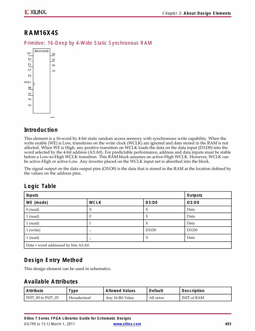
Chapter 3: About Design Elements
RAM16X4SPrimitive: 16-Deep by 4-Wide Static Synchronous RAM
IntroductionThis element is a 16-word by 4-bit static random access memory with synchronous write capability. When thewrite enable (WE) is Low, transitions on the write clock (WCLK) are ignored and data stored in the RAM is notaffected. When WE is High, any positive transition on WCLK loads the data on the data input (D3:D0) into theword selected by the 4-bit address (A3:A0). For predictable performance, address and data inputs must be stablebefore a Low-to-High WCLK transition. This RAM block assumes an active-High WCLK. However, WCLK canbe active-High or active-Low. Any inverter placed on the WCLK input net is absorbed into the block.
The signal output on the data output pins (O3:O0) is the data that is stored in the RAM at the location defined bythe values on the address pins.
Logic TableInputs Outputs
WE (mode) WCLK D3:D0 O3:O00 (read) X X Data
1 (read) 0 X Data
1 (read) 1 X Data
1 (write) ↑ D3:D0 D3:D0
1 (read) ↓ X Data
Data = word addressed by bits A3:A0.
Design Entry MethodThis design element can be used in schematics.
Available AttributesAttribute Type Allowed Values Default DescriptionINIT_00 to INIT_03 Hexadecimal Any 16-Bit Value All zeros INIT of RAM
Xilinx 7 Series FPGA Libraries Guide for Schematic DesignsUG799 (v 13.1) March 1, 2011 www.xilinx.com 493

Chapter 3: About Design Elements
For More InformationSee the 7 series FPGA User Documentation (User Guides and Data Sheets).
Xilinx 7 Series FPGA Libraries Guide for Schematic Designs494 www.xilinx.com UG799 (v 13.1) March 1, 2011

Chapter 3: About Design Elements
RAM16X8SPrimitive: 16-Deep by 8-Wide Static Synchronous RAM
IntroductionThis element is a 16-word by 8-bit static random access memory with synchronous write capability. When thewrite enable (WE) is Low, transitions on the write clock (WCLK) are ignored and data stored in the RAM is notaffected. When WE is High, any positive transition on WCLK loads the data on data inputs (D7:D0) into theword selected by the 4-bit address (A3:A0). For predictable performance, address and data inputs must be stablebefore a Low-to-High WCLK transition. This RAM block assumes an active-High WCLK. However, WCLK canbe active-High or active-Low. Any inverter placed on the WCLK input net is absorbed into the block.
The signal output on the data output pins (O7:O0) is the data that is stored in the RAM at the location defined bythe values on the address pins.
Logic TableInputs Outputs
WE (mode) WCLK D7:D0 O7:O00 (read) X X Data
1 (read) 0 X Data
1 (read) 1 X Data
1 (write) ↑ D7:D0 D7:D0
1 (read) ↓ X Data
Data = word addressed by bits A3–A0
Design Entry MethodThis design element can be used in schematics.
Available AttributesAttribute Type Allowed Values Default DescriptionINIT_00 to INIT_07 Hexadecimal Any 16-Bit Value All zeros Initializes RAMs, registers, and look-up
tables.
For More InformationSee the 7 series FPGA User Documentation (User Guides and Data Sheets).
Xilinx 7 Series FPGA Libraries Guide for Schematic DesignsUG799 (v 13.1) March 1, 2011 www.xilinx.com 495

Chapter 3: About Design Elements
RAM256X1SPrimitive: 256-Deep by 1-Wide Random Access Memory (Select RAM)
IntroductionThis design element is a 256-bit deep by 1-bit wide random access memory with synchronous write andasynchronous read capability. This RAM is implemented using the LUT resources of the device (also knownas Select RAM), and does not consume any of the block RAM resources of the device. If a synchronous readcapability is preferred, a register can be attached to the output and placed in the same slice as long as thesame clock is used for both the RAM and the register. The RAM256X1S has an active, High write enable, WE,so that when that signal is High, and a rising edge occurs on the WCLK pin, a write is performed recordingthe value of the D input data pin into the memory array. The output O displays the contents of the memorylocation addressed by A, regardless of the WE value. When a write is performed, the output is updated to thenew value shortly after the write completes.
Port DescriptionsPort Direction Width FunctionO Output 1 Read/Write port data output addressed by A
D Input 1 Write data input addressed by A
A Input 8 Read/Write port address bus
WE Input 1 Write Enable
WCLK Input 1 Write clock (reads are asynchronous)
Design Entry MethodIf instantiated, the following connections should be made to this component:• Tie the WCLK input to the desired clock source, the D input to the data source to be stored, and the O output
to an FDCE D input or other appropriate data destination.• The WE clock enable pin should be connected to the proper write enable source in the design.• The 8-bit A bus should be connected to the source for the read/write.• An optional INIT attribute consisting of a 256-bit Hexadecimal value can be specified to indicate the initial
contents of the RAM.
If left unspecified, the initial contents default to all zeros.
Available AttributesAttribute Type Allowed Values Default DescriptionINIT Hexadecimal Any 256-Bit Value All
zerosSpecifies the initial contents of the RAM.
For More InformationSee the 7 series FPGA User Documentation (User Guides and Data Sheets).
Xilinx 7 Series FPGA Libraries Guide for Schematic Designs496 www.xilinx.com UG799 (v 13.1) March 1, 2011
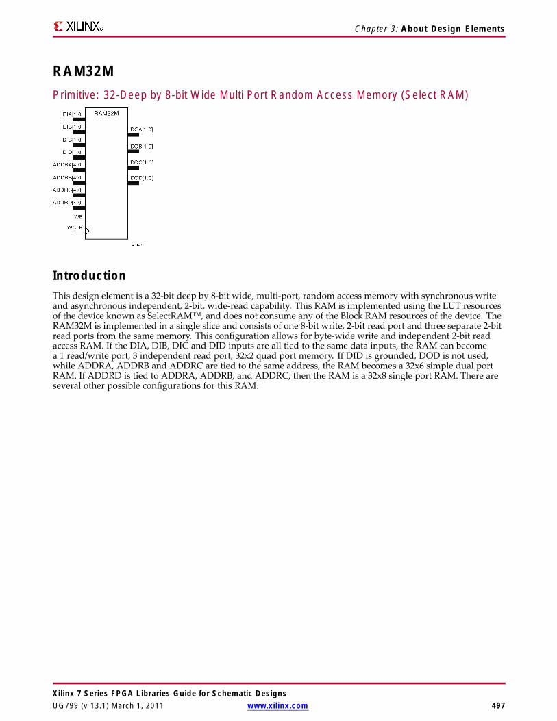
Chapter 3: About Design Elements
RAM32MPrimitive: 32-Deep by 8-bit Wide Multi Port Random Access Memory (Select RAM)
IntroductionThis design element is a 32-bit deep by 8-bit wide, multi-port, random access memory with synchronous writeand asynchronous independent, 2-bit, wide-read capability. This RAM is implemented using the LUT resourcesof the device known as SelectRAM™, and does not consume any of the Block RAM resources of the device. TheRAM32M is implemented in a single slice and consists of one 8-bit write, 2-bit read port and three separate 2-bitread ports from the same memory. This configuration allows for byte-wide write and independent 2-bit readaccess RAM. If the DIA, DIB, DIC and DID inputs are all tied to the same data inputs, the RAM can becomea 1 read/write port, 3 independent read port, 32x2 quad port memory. If DID is grounded, DOD is not used,while ADDRA, ADDRB and ADDRC are tied to the same address, the RAM becomes a 32x6 simple dual portRAM. If ADDRD is tied to ADDRA, ADDRB, and ADDRC, then the RAM is a 32x8 single port RAM. There areseveral other possible configurations for this RAM.
Xilinx 7 Series FPGA Libraries Guide for Schematic DesignsUG799 (v 13.1) March 1, 2011 www.xilinx.com 497

Chapter 3: About Design Elements
Port DescriptionsPort Direction Width FunctionDOA Output 2 Read port data outputs addressed by ADDRA
DOB Output 2 Read port data outputs addressed by ADDRB
DOC Output 2 Read port data outputs addressed by ADDRC
DOD Output 2 Read/Write port data outputs addressed by ADDRD
DIA Input 2 Write data inputs addressed by ADDRD (read output isaddressed by ADDRA)
DIB Input 2 Write data inputs addressed by ADDRD (read output isaddressed by ADDRB)
DIC Input 2 Write data inputs addressed by ADDRD (read output isaddressed by ADDRC)
DID Input 2 Write data inputs addressed by ADDRD
ADDRA Input 5 Read address bus A
ADDRB Input 5 Read address bus B
ADDRC Input 5 Read address bus C
ADDRD Input 5 8-bit data write port, 2-bit data read port address bus D
WE Input 1 Write Enable
WCLK Input 1 Write clock (reads are asynchronous)
Design Entry MethodThis design element can be used in schematics.
This element can be inferred by some synthesis tools by describing a RAM with a synchronous write andasynchronous read capability. Consult your synthesis tool documentation for details on RAM inferencecapabilities and coding examples. Xilinx suggests that you instantiate RAM32Ms if you have a need to implicitlyspecify the RAM function, or if you need to manually place or relationally place the component. If a synchronousread capability is desired, the RAM32M outputs can be connected to an FDRSE (FDCPE is asynchronous set/resetis necessary) in order to improve the output timing of the function. However, this is not necessary for theproper operation of the RAM.
If you want to have the data clocked on the negative edge of a clock, an inverter can be described on the clockinput to this component. This inverter will be absorbed into the block, giving you the ability to write to the RAMon falling clock edges.
If instantiated, the following connections should be made to this component. Tie the WCLK input to the desiredclock source, the DIA, DIB, DIC and DID inputs to the data source to be stored and the DOA, DOB, DOC andDOD outputs to an FDCE D input or other appropriate data destination or left unconnected if not used. The WEclock enable pin should be connected to the proper write enable source in the design. The 5-bit ADDRD busshould be connected to the source for the read/write addressing and the 5-bit ADDRA, ADDRB and ADDRCbuses should be connected to the appropriate read address connections. The optional INIT_A, INIT_B, INIT_Cand INIT_D attributes consisting of a 64-bit hexadecimal values that specifies each port’s initial memory contentscan be specified. The INIT value correlates to the RAM addressing by the following equation: ADDRy[z] =INIT_y[2*z+1:2*z]. For instance, if the RAM ADDRC port is addressed to 00001, then the INIT_C[3:2] valueswould be the initial values shown on the DOC port before the first write occurs at that address. If left unspecified,the initial contents will default to all zeros.
Xilinx 7 Series FPGA Libraries Guide for Schematic Designs498 www.xilinx.com UG799 (v 13.1) March 1, 2011
Chapter 3: About Design Elements
Available AttributesAttribute Type Allowed Values Default DescriptionINIT_A Hexadecimal Any 64-Bit Value All zeros Specifies the initial contents of the RAM on
the A port.
INIT_B Hexadecimal Any 64-Bit Value All zeros Specifies the initial contents of the RAM onthe B port.
INIT_C Hexadecimal Any 64-Bit Value All zeros Specifies the initial contents of the RAM onthe C port.
INIT_D Hexadecimal Any 64-Bit Value All zeros Specifies the initial contents of the RAM onthe D port.
For More InformationSee the 7 series FPGA User Documentation (User Guides and Data Sheets).
Xilinx 7 Series FPGA Libraries Guide for Schematic DesignsUG799 (v 13.1) March 1, 2011 www.xilinx.com 499

Chapter 3: About Design Elements
RAM32X1DPrimitive: 32-Deep by 1-Wide Static Dual Port Synchronous RAM
IntroductionThe design element is a 32-word by 1-bit static dual port random access memory with synchronous writecapability. The device has two separate address ports: the read address (DPRA4:DPRA0) and the write address(A4:A0). These two address ports are completely asynchronous. The read address controls the location ofthe data driven out of the output pin (DPO), and the write address controls the destination of a valid writetransaction. When the write enable (WE) is Low, transitions on the write clock (WCLK) are ignored and datastored in the RAM is not affected. When WE is High, any positive transition on WCLK loads the data on thedata input (D) into the word selected by the 5-bit write address. For predictable performance, write address anddata inputs must be stable before a Low-to-High WCLK transition. This RAM block assumes an active-HighWCLK. WCLK can be active-High or active-Low. Any inverter placed on the WCLK input net is absorbed intothe block. You can initialize RAM32X1D during configuration using the INIT attribute. Mode selection isshown in the following logic table.
The SPO output reflects the data in the memory cell addressed by A4:A0. The DPO output reflects the data inthe memory cell addressed by DPRA4:DPRA0. The write process is not affected by the address on the readaddress port.
Logic TableInputs Outputs
WE (Mode) WCLK D SPO DPO0 (read) X X data_a data_d
1 (read) 0 X data_a data_d
1 (read) 1 X data_a data_d
1 (write) ↑ D D data_d
1 (read) ↓ X data_a data_d
Design Entry MethodThis design element can be used in schematics.
Xilinx 7 Series FPGA Libraries Guide for Schematic Designs500 www.xilinx.com UG799 (v 13.1) March 1, 2011

Chapter 3: About Design Elements
Available Attributes
Attribute TypeAllowedValues Default Descriptions
INIT Hexadecimal Any 32-BitValue
All Zeros Initializes ROMs, RAMs, registers, and look-uptables.
For More InformationSee the 7 series FPGA User Documentation (User Guides and Data Sheets).
Xilinx 7 Series FPGA Libraries Guide for Schematic DesignsUG799 (v 13.1) March 1, 2011 www.xilinx.com 501
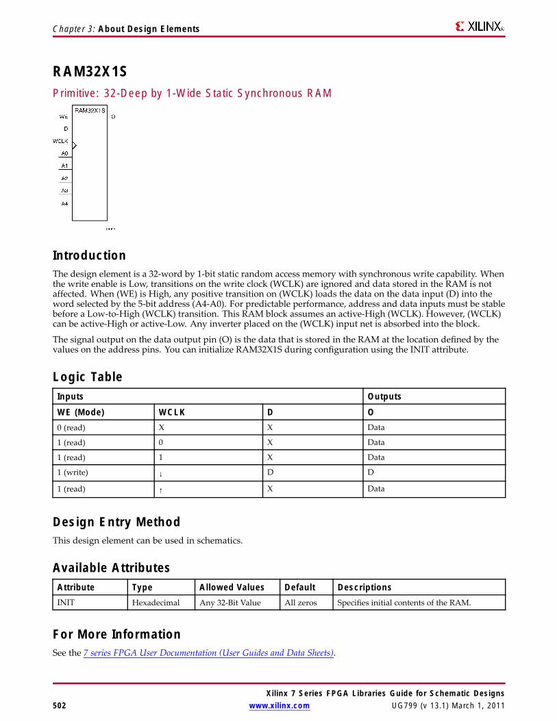
Chapter 3: About Design Elements
RAM32X1SPrimitive: 32-Deep by 1-Wide Static Synchronous RAM
IntroductionThe design element is a 32-word by 1-bit static random access memory with synchronous write capability. Whenthe write enable is Low, transitions on the write clock (WCLK) are ignored and data stored in the RAM is notaffected. When (WE) is High, any positive transition on (WCLK) loads the data on the data input (D) into theword selected by the 5-bit address (A4-A0). For predictable performance, address and data inputs must be stablebefore a Low-to-High (WCLK) transition. This RAM block assumes an active-High (WCLK). However, (WCLK)can be active-High or active-Low. Any inverter placed on the (WCLK) input net is absorbed into the block.
The signal output on the data output pin (O) is the data that is stored in the RAM at the location defined by thevalues on the address pins. You can initialize RAM32X1S during configuration using the INIT attribute.
Logic TableInputs Outputs
WE (Mode) WCLK D O0 (read) X X Data
1 (read) 0 X Data
1 (read) 1 X Data
1 (write) ↓ D D
1 (read) ↑ X Data
Design Entry MethodThis design element can be used in schematics.
Available AttributesAttribute Type Allowed Values Default DescriptionsINIT Hexadecimal Any 32-Bit Value All zeros Specifies initial contents of the RAM.
For More InformationSee the 7 series FPGA User Documentation (User Guides and Data Sheets).
Xilinx 7 Series FPGA Libraries Guide for Schematic Designs502 www.xilinx.com UG799 (v 13.1) March 1, 2011

Chapter 3: About Design Elements
RAM32X1S_1Primitive: 32-Deep by 1-Wide Static Synchronous RAM with Negative-Edge Clock
IntroductionThe design element is a 32-word by 1-bit static random access memory with synchronous write capability. Whenthe write enable is Low, transitions on the write clock (WCLK) are ignored and data stored in the RAM is notaffected. When (WE) is High, any negative transition on (WCLK) loads the data on the data input (D) into theword selected by the 5-bit address (A4:A0). For predictable performance, address and data inputs must be stablebefore a High-to-Low (WCLK) transition. This RAM block assumes an active-Low (WCLK). However, (WCLK)can be active-High or active-Low. Any inverter placed on the (WCLK) input net is absorbed into the block.
The signal output on the data output pin (O) is the data that is stored in the RAM at the location defined by thevalues on the address pins. You can initialize RAM32X1S_1 during configuration using the INIT attribute.
Logic TableInputs Outputs
WE (Mode) WCLK D O0 (read) X X Data
1 (read) 0 X Data
1 (read) 1 X Data
1 (write) ↓ D D
1 (read) ↑ X Data
Data = word addressed by bits A4:A0
Design Entry MethodThis design element can be used in schematics.
Available AttributesAttribute Type Allowed Values Default DescriptionsINIT Hexadecimal Any 32-Bit Value 0 Initializes RAMs, registers, and look-up
tables.
For More InformationSee the 7 series FPGA User Documentation (User Guides and Data Sheets).
Xilinx 7 Series FPGA Libraries Guide for Schematic DesignsUG799 (v 13.1) March 1, 2011 www.xilinx.com 503

Chapter 3: About Design Elements
RAM32X2SPrimitive: 32-Deep by 2-Wide Static Synchronous RAM
IntroductionThe design element is a 32-word by 2-bit static random access memory with synchronous write capability. Whenthe write enable (WE) is Low, transitions on the write clock (WCLK) are ignored and data stored in the RAM isnot affected. When (WE) is High, any positive transition on (WCLK) loads the data on the data input (D1-D0)into the word selected by the 5-bit address (A4-A0). For predictable performance, address and data inputs mustbe stable before a Low-to-High (WCLK) transition. This RAM block assumes an active-High (WCLK). However,(WCLK) can be active-High or active-Low. Any inverter placed on the (WCLK) input net is absorbed into theblock. The signal output on the data output pins (O1-O0) is the data that is stored in the RAM at the locationdefined by the values on the address pins.
You can use the INIT_00 and INIT_01 properties to specify the initial contents of RAM32X2S.
Logic TableInputs Outputs
WE (Mode) WCLK D O0-O10 (read) X X Data
1 (read) 0 X Data
1 (read) 1 X Data
1 (write) ↑ D1:D0 D1:D0
1 (read) ↓ X Data
Data = word addressed by bits A4:A0
Design Entry MethodThis design element can be used in schematics.
Available AttributesAttribute Type Allowed Values Default DescriptionsINIT_00 Hexadecimal Any 32-Bit Value All zeros INIT for bit 0 of RAM.
INIT_01 Hexadecimal Any 32-Bit Value All zeros INIT for bit 1 of RAM.
Xilinx 7 Series FPGA Libraries Guide for Schematic Designs504 www.xilinx.com UG799 (v 13.1) March 1, 2011

Chapter 3: About Design Elements
For More InformationSee the 7 series FPGA User Documentation (User Guides and Data Sheets).
Xilinx 7 Series FPGA Libraries Guide for Schematic DesignsUG799 (v 13.1) March 1, 2011 www.xilinx.com 505

Chapter 3: About Design Elements
RAM32X4SPrimitive: 32-Deep by 4-Wide Static Synchronous RAM
IntroductionThis design element is a 32-word by 4-bit static random access memory with synchronous write capability. Whenthe write enable (WE) is Low, transitions on the write clock (WCLK) are ignored and data stored in the RAM isnot affected. When WE is High, any positive transition on WCLK loads the data on the data inputs (D3-D0)into the word selected by the 5-bit address (A4:A0). For predictable performance, address and data inputs mustbe stable before a Low-to-High WCLK transition. This RAM block assumes an active-High WCLK. However,WCLK can be active-High or active-Low. Any inverter placed on the WCLK input net is absorbed into the block.
The signal output on the data output pins (O3-O0) is the data that is stored in the RAM at the location defined bythe values on the address pins.
Logic TableInputs Outputs
WE WCLK D3-D0 O3-O00 (read) X X Data
1 (read) 0 X Data
1 (read) 1 X Data
1 (write) ↑ D3:D0 D3:D0
1 (read) ↓ X Data
Data = word addressed by bits A4:A0
Design Entry MethodThis design element can be used in schematics.
Xilinx 7 Series FPGA Libraries Guide for Schematic Designs506 www.xilinx.com UG799 (v 13.1) March 1, 2011
Chapter 3: About Design Elements
Available AttributesAttribute Type Allowed Values Default DescriptionINIT_00 Hexadecimal Any 32-Bit Value All zeros INIT for bit 0 of RAM.
INIT_01 Hexadecimal Any 32-Bit Value All zeros INIT for bit 1 of RAM.
INIT_02 Hexadecimal Any 32-Bit Value All zeros INIT for bit 2 of RAM.
INIT_03 Hexadecimal Any 32-Bit Value All zeros INIT for bit 3 of RAM.
For More InformationSee the 7 series FPGA User Documentation (User Guides and Data Sheets).
Xilinx 7 Series FPGA Libraries Guide for Schematic DesignsUG799 (v 13.1) March 1, 2011 www.xilinx.com 507
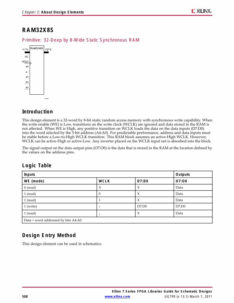
Chapter 3: About Design Elements
RAM32X8SPrimitive: 32-Deep by 8-Wide Static Synchronous RAM
IntroductionThis design element is a 32-word by 8-bit static random access memory with synchronous write capability. Whenthe write enable (WE) is Low, transitions on the write clock (WCLK) are ignored and data stored in the RAM isnot affected. When WE is High, any positive transition on WCLK loads the data on the data inputs (D7:D0)into the word selected by the 5-bit address (A4:A0). For predictable performance, address and data inputs mustbe stable before a Low-to-High WCLK transition. This RAM block assumes an active-High WCLK. However,WCLK can be active-High or active-Low. Any inverter placed on the WCLK input net is absorbed into the block.
The signal output on the data output pins (O7:O0) is the data that is stored in the RAM at the location defined bythe values on the address pins.
Logic TableInputs Outputs
WE (mode) WCLK D7:D0 O7:O00 (read) X X Data
1 (read) 0 X Data
1 (read) 1 X Data
1 (write) ↑ D7:D0 D7:D0
1 (read) ↓ X Data
Data = word addressed by bits A4:A0
Design Entry MethodThis design element can be used in schematics.
Xilinx 7 Series FPGA Libraries Guide for Schematic Designs508 www.xilinx.com UG799 (v 13.1) March 1, 2011
Chapter 3: About Design Elements
Available AttributesAttribute Type Allowed Values Default DescriptionINIT_00 Hexadecimal Any 32-Bit Value All zeros INIT for bit 0 of RAM.
INIT_01 Hexadecimal Any 32-Bit Value All zeros INIT for bit 1 of RAM.
INIT_02 Hexadecimal Any 32-Bit Value All zeros INIT for bit 2 of RAM.
INIT_03 Hexadecimal Any 32-Bit Value All zeros INIT for bit 3 of RAM.
INIT_04 Hexadecimal Any 32-Bit Value All zeros INIT for bit 4 of RAM.
INIT_05 Hexadecimal Any 32-Bit Value All zeros INIT for bit 5 of RAM.
INIT_06 Hexadecimal Any 32-Bit Value All zeros INIT for bit 6 of RAM.
INIT_07 Hexadecimal Any 32-Bit Value All zeros INIT for bit 7 of RAM.
For More InformationSee the 7 series FPGA User Documentation (User Guides and Data Sheets).
Xilinx 7 Series FPGA Libraries Guide for Schematic DesignsUG799 (v 13.1) March 1, 2011 www.xilinx.com 509
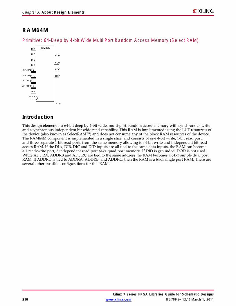
Chapter 3: About Design Elements
RAM64MPrimitive: 64-Deep by 4-bit Wide Multi Port Random Access Memory (Select RAM)
IntroductionThis design element is a 64-bit deep by 4-bit wide, multi-port, random access memory with synchronous writeand asynchronous independent bit wide read capability. This RAM is implemented using the LUT resources ofthe device (also known as SelectRAM™) and does not consume any of the block RAM resources of the device.The RAM64M component is implemented in a single slice, and consists of one 4-bit write, 1-bit read port,and three separate 1-bit read ports from the same memory allowing for 4-bit write and independent bit readaccess RAM. If the DIA, DIB, DIC and DID inputs are all tied to the same data inputs, the RAM can becomea 1 read/write port, 3 independent read port 64x1 quad port memory. If DID is grounded, DOD is not used.While ADDRA, ADDRB and ADDRC are tied to the same address the RAM becomes a 64x3 simple dual portRAM. If ADDRD is tied to ADDRA, ADDRB, and ADDRC; then the RAM is a 64x4 single port RAM. There areseveral other possible configurations for this RAM.
Xilinx 7 Series FPGA Libraries Guide for Schematic Designs510 www.xilinx.com UG799 (v 13.1) March 1, 2011

Chapter 3: About Design Elements
Port DescriptionsPort Direction Width FunctionDOA Output 1 Read port data outputs addressed by ADDRA
DOB Output 1 Read port data outputs addressed by ADDRB
DOC Output 1 Read port data outputs addressed by ADDRC
DOD Output 1 Read/Write port data outputs addressed byADDRD
DIA Input 1 Write data inputs addressed by ADDRD (readoutput is addressed by ADDRA)
DIB Input 1 Write data inputs addressed by ADDRD (readoutput is addressed by ADDRB)
DIC Input 1 Write data inputs addressed by ADDRD (readoutput is addressed by ADDRC)
DID Input 1 Write data inputs addressed by ADDRD
ADDRA Input 6 Read address bus A
ADDRB Input 6 Read address bus B
ADDRC Input 6 Read address bus C
ADDRD Input 6 4-bit data write port, 1-bit data read portaddress bus D
WE Input 1 Write Enable
WCLK Input 1 Write clock (reads are asynchronous)
Design Entry MethodThis design element can be used in schematics.
This element can be inferred by some synthesis tools by describing a RAM with a synchronous write andasynchronous read capability. Consult your synthesis tool documentation for details on RAM inferencecapabilities and coding examples. Xilinx suggests that you instantiate RAM64Ms if you have a need to implicitlyspecify the RAM function, or if you need to manually place or relationally place the component. If a synchronousread capability is desired, the RAM64M outputs can be connected to an FDRSE (FDCPE is asynchronous set/resetis necessary) in order to improve the output timing of the function. However, this is not necessary for theproper operation of the RAM. If you want to have the data clocked on the negative edge of a clock, an invertercan be described on the clock input to this component. This inverter will be absorbed into the block giving theability to write to the RAM on falling clock edges.
If instantiated, the following connections should be made to this component. Tie the WCLK input to thedesired clock source, the DIA, DIB, DIC and DID inputs to the data source to be stored and the DOA, DOB,DOC and DOD outputs to an FDCE D input or other appropriate data destination or left unconnected if notused. The WE clock enable pin should be connected to the proper write enable source in the design. The 5-bitADDRD bus should be connected to the source for the read/write addressing and the 5-bit ADDRA, ADDRBand ADDRC buses should be connected to the appropriate read address connections. The optional INIT_A,INIT_B, INIT_C and INIT_D attributes consisting of a 64-bit hexadecimal values that specifies each port’s initialmemory contents can be specified. The INIT value correlates to the RAM addressing by the following equation:ADDRy[z] = INIT_y[z].
For instance, if the RAM ADDRC port is addressed to 00001, then the INIT_C[1] values would be the initialvalues shown on the DOC port before the first write occurs at that address. If left unspecified, the initial contentswill default to all zeros.
Xilinx 7 Series FPGA Libraries Guide for Schematic DesignsUG799 (v 13.1) March 1, 2011 www.xilinx.com 511

Chapter 3: About Design Elements
Available AttributesAttribute Type Allowed Values Default DescriptionINIT_A Hexadecimal Any 64-Bit Value All zero Specifies the initial contents of the RAM on
the A port.
INIT_B Hexadecimal Any 64-Bit Value All zero Specifies the initial contents of the RAM onthe B port.
INIT_C Hexadecimal Any 64-Bit Value All zero Specifies the initial contents of the RAM onthe C port.
INIT_D Hexadecimal Any 64-Bit Value All zero Specifies the initial contents of the RAM onthe D port.
For More Information
Xilinx 7 Series FPGA Libraries Guide for Schematic Designs512 www.xilinx.com UG799 (v 13.1) March 1, 2011

Chapter 3: About Design Elements
RAM64X1DPrimitive: 64-Deep by 1-Wide Dual Port Static Synchronous RAM
IntroductionThis design element is a 64-word by 1-bit static dual port random access memory with synchronous writecapability. The device has two separate address ports: the read address (DPRA5:DPRA0) and the write address(A5:A0). These two address ports are completely asynchronous. The read address controls the location ofthe data driven out of the output pin (DPO), and the write address controls the destination of a valid writetransaction. When the write enable (WE) is Low, transitions on the write clock (WCLK) are ignored and datastored in the RAM is not affected.
When WE is High, any positive transition on WCLK loads the data on the data input (D) into the word selectedby the 6-bit (A0:A5) write address. For predictable performance, write address and data inputs must be stablebefore a Low-to-High WCLK transition. This RAM block assumes an active-High WCLK. WCLK can beactive-High or active-Low. Any inverter placed on the WCLK input net is absorbed into the block.
The SPO output reflects the data in the memory cell addressed by A5:A0. The DPO output reflects the datain the memory cell addressed by DPRA5:DPRA0.
Note The write process is not affected by the address on the read address port.
Logic TableInputs Outputs
WE (mode) WCLK D SPO DPO0 (read) X X data_a data_d
1 (read) 0 X data_a data_d
1 (read) 1 X data_a data_d
1 (write) ↑ D D data_d
1 (read) ↓ X data_a data_d
data_a = word addressed by bits A5:A0
data_d = word addressed by bits DPRA5:DPRA0
Design Entry MethodThis design element can be used in schematics.
Xilinx 7 Series FPGA Libraries Guide for Schematic DesignsUG799 (v 13.1) March 1, 2011 www.xilinx.com 513

Chapter 3: About Design Elements
Available Attributes
Attribute TypeAllowedValues Default Description
INIT Hexadecimal Any 64-BitValue
All zeros Initializes RAMs, registers, and look-up tables.
For More InformationSee the 7 series FPGA User Documentation (User Guides and Data Sheets).
Xilinx 7 Series FPGA Libraries Guide for Schematic Designs514 www.xilinx.com UG799 (v 13.1) March 1, 2011

Chapter 3: About Design Elements
RAM64X1SPrimitive: 64-Deep by 1-Wide Static Synchronous RAM
IntroductionThis design element is a 64-word by 1-bit static random access memory (RAM) with synchronous write capability.When the write enable is set Low, transitions on the write clock (WCLK) are ignored and data stored in the RAMis not affected. When WE is set High, any positive transition on WCLK loads the data on the data input (D)into the word selected by the 6-bit address (A5:A0). This RAM block assumes an active-High WCLK. However,WCLK can be active-High or active-Low. Any inverter placed on the WCLK input net is absorbed into the block.
The signal output on the data output pin (O) is the data that is stored in the RAM at the location defined bythe values on the address pins.
You can initialize this element during configuration using the INIT attribute.
Logic TableMode selection is shown in the following logic table
Inputs Outputs
WE (mode) WCLK D O0 (read) X X Data
1 (read) 0 X Data
1 (read) 1 X Data
1 (write) ↑ D D
1 (read) ↓ X Data
Data = word addressed by bits A5:A0
Design Entry MethodThis design element can be used in schematics.
Available Attributes
Attribute TypeAllowedValues Default Description
INIT Hexadecimal Any 64-Bit Value All zeros Initializes ROMs, RAMs, registers, and look-uptables.
Xilinx 7 Series FPGA Libraries Guide for Schematic DesignsUG799 (v 13.1) March 1, 2011 www.xilinx.com 515

Chapter 3: About Design Elements
For More InformationSee the 7 series FPGA User Documentation (User Guides and Data Sheets).
Xilinx 7 Series FPGA Libraries Guide for Schematic Designs516 www.xilinx.com UG799 (v 13.1) March 1, 2011

Chapter 3: About Design Elements
RAM64X1S_1Primitive: 64-Deep by 1-Wide Static Synchronous RAM with Negative-Edge Clock
IntroductionThis design element is a 64-word by 1-bit static random access memory with synchronous write capability. Whenthe write enable is Low, transitions on the write clock (WCLK) are ignored and data stored in the RAM is notaffected. When (WE) is High, any negative transition on (WCLK) loads the data on the data input (D) into theword selected by the 6-bit address (A5:A0). For predictable performance, address and data inputs must be stablebefore a High-to-Low (WCLK) transition. This RAM block assumes an active-Low (WCLK). However, (WCLK)can be active-High or active-Low. Any inverter placed on the (WCLK) input net is absorbed into the block.
The signal output on the data output pin (O) is the data that is stored in the RAM at the location defined bythe values on the address pins.
You can initialize this element during configuration using the INIT attribute.
Logic TableInputs Outputs
WE (mode) WCLK D O0 (read) X X Data
1 (read) 0 X Data
1 (read) 1 X Data
1 (write) ↓ D D
1 (read) ↑ X Data
Data = word addressed by bits A5:A0
Design Entry MethodThis design element can be used in schematics.
Available AttributesAttribute Type Allowed Values Default DescriptionINIT Hexadecimal Any 64-Bit Value All zeros Initializes ROMs, RAMs, registers, and look-up
tables.
For More InformationSee the 7 series FPGA User Documentation (User Guides and Data Sheets).
Xilinx 7 Series FPGA Libraries Guide for Schematic DesignsUG799 (v 13.1) March 1, 2011 www.xilinx.com 517

Chapter 3: About Design Elements
RAM64X2SPrimitive: 64-Deep by 2-Wide Static Synchronous RAM
IntroductionThis design element is a 64-word by 2-bit static random access memory with synchronous write capability. Whenthe write enable (WE) is Low, transitions on the write clock (WCLK) are ignored and data stored in the RAMis not affected. When WE is High, any positive transition on WCLK loads the data on the data input (D1:D0)into the word selected by the 6-bit address (A5:A0). For predictable performance, address and data inputs mustbe stable before a Low-to-High WCLK transition. This RAM block assumes an active-High WCLK. However,WCLK can be active-High or active-Low. Any inverter placed on the WCLK input net is absorbed into the block.
The signal output on the data output pins (O1:O0) is the data that is stored in the RAM at the location defined bythe values on the address pins. You can use the INIT_00 and INIT_01 properties to specify the initial contentsof this design element.
Logic TableInputs OutputsWE (mode) WCLK D0:D1 O0:O1
0 (read) X X Data
1 (read) 0 X Data
1 (read) 1 X Data
1 (write) ↑ D1:D0 D1:D0
1 (read) ↓ X Data
Data = word addressed by bits A5:A0
Design Entry MethodThis design element can be used in schematics.
Available AttributesAttribute Type Allowed Values Default DescriptionINIT_00 Hexadecimal Any 64-Bit Value All zeros Initializes RAMs, registers, and look-up tables.
INIT_01 Hexadecimal Any 64-Bit Value All zeros Initializes RAMs, registers, and look-up tables.
Xilinx 7 Series FPGA Libraries Guide for Schematic Designs518 www.xilinx.com UG799 (v 13.1) March 1, 2011

Chapter 3: About Design Elements
For More InformationSee the 7 series FPGA User Documentation (User Guides and Data Sheets).
Xilinx 7 Series FPGA Libraries Guide for Schematic DesignsUG799 (v 13.1) March 1, 2011 www.xilinx.com 519

Chapter 3: About Design Elements
RAMB18E1Primitive: 18K-bit Configurable Synchronous Block RAM
Introduction7 series devices contain several block RAMmemories that can be configured as FIFOs, automatic error correctionRAM, or general-purpose 36KB or 18KB RAM/ROM memories. These block RAM memories offer fast andflexible storage of large amounts of on-chip data. The RAMB18E1 allows access to the block RAM in the 18KBconfiguration. This element can be configured and used as a 1-bit wide by 16K deep to an 18-bit wide by 1024-bitdeep true dual port RAM. This element can also be configured as a 36-bit wide by 512 deep simple dual portRAM. Both read and write operations are fully synchronous to the supplied clock(s) to the component. However,the READ and WRITE ports can operate fully independent and asynchronous to each other, accessing the samememory array. When configured in the wider data width modes, byte-enable write operations are possible, andan optional output register can be used to reduce the clock-to-out times of the RAM.
Port DescriptionsPort Type Width FunctionADDRARDADDR<13:0> Input 14 Port A address input bus/Read address input bus. Port A
address and control (clock, reset, enables, etc.) signals whenRAM_MODE="TDP". When RAM_MODE="SDP" these are theread port address and control signals.
Xilinx 7 Series FPGA Libraries Guide for Schematic Designs520 www.xilinx.com UG799 (v 13.1) March 1, 2011

Chapter 3: About Design Elements
Port Type Width FunctionADDRBWRADDR<13:0> Input 14 Port B address input bus/Write address input bus. Port B data
signals when RAM_MODE="TDP". When RAM_MODE="SDP"these are the MSB data signals.
CLKARDCLK Input 1 Rising edge port A clock input/Read clock input. Port Aaddress and control (clock, reset, enables, etc.) signals whenRAM_MODE="TDP". When RAM_MODE="SDP" these are theread port address and control signals.
CLKBWRCLK Input 1 Rising edge port B clock input/Write clock input. Port B datasignals when RAM_MODE="TDP". When RAM_MODE="SDP"these are the MSB data signals.
DIADI<15:0> Input 16 Port A data input bus/Data input bus addressed by WRADDR.When RAM_MODE="SDP", DIADI is the logical DI<15:0>.Port A data signals when RAM_MODE="TDP". WhenRAM_MODE="SDP" these are the LSB data signals.
DIBDI<15:0> Input 16 Port B data input bus/Data input bus addressed by WRADDR.When RAM_MODE="SDP", DIBDI is the logical DI<31:16>.Port B data signals when RAM_MODE="TDP". WhenRAM_MODE="SDP" these are the MSB data signals.
DIPADIP<1:0> Input 2 Port A parity data input bus/Data parity input bus addressed byWRADDR. When RAM_MODE="SDP", DIPADIP is the logicalDIP<1:0>. Port A data signals when RAM_MODE="TDP". WhenRAM_MODE="SDP" these are the LSB data signals.
DIPBDIP<1:0> Input 2 Port B parity data input bus/Data parity input bus addressed byWRADDR. When RAM_MODE="SDP", DIPBDIP is the logicalDIP<3:2>. Port B data signals when RAM_MODE="TDP". WhenRAM_MODE="SDP" these are the MSB data signals.
DOADO<15:0> Output 16 Port A data output bus/Data output bus addressed by RDADDR.When RAM_MODE="SDP", DOADO is the logical DO<15:0>.Port A data signals when RAM_MODE="TDP". WhenRAM_MODE="SDP" these are the LSB data signals.
DOBDO<15:0> Output 16 Port B data output bus/Data output bus addressed by RDADDR.When RAM_MODE="SDP", DOBDO is the logical DO<31:16>.Port B data signals when RAM_MODE="TDP". WhenRAM_MODE="SDP" these are the MSB data signals.
DOPADOP<1:0> Output 2 Port A parity data output bus/Data parity output bus addressed byRDADDR. When RAM_MODE="SDP", DOPADOP is the logicalDOP<1:0>. Port A data signals when RAM_MODE="TDP". WhenRAM_MODE="SDP" these are the LSB data signals.
DOPBDOP<1:0> Output 2 Port B parity data output bus/Data parity output bus addressed byRDADDR. When RAM_MODE="SDP", DOPBDOP is the logicalDOP<3:2>. Port B data signals when RAM_MODE="TDP". WhenRAM_MODE="SDP" these are the MSB data signals.
ENARDEN Input 1 Port A RAM enable. Port A address and control (clock, reset,enables, etc.) signals when RAM_MODE="TDP". WhenRAM_MODE="SDP" these are the read port address and controlsignals.
ENBWREN Input 1 Port B RAM enable/Write enable. Port B address and control(clock, reset, enables, etc.) signals when RAM_MODE="TDP".When RAM_MODE="SDP" these are the write port address andcontrol signals.
REGCEAREGCE Input 1 Port A output register clock enable input (valid only whenDO_REG=1). Port A address and control (clock, reset, enables, etc.)signals when RAM_MODE="TDP". When RAM_MODE="SDP"these are the read port address and control signals.
Xilinx 7 Series FPGA Libraries Guide for Schematic DesignsUG799 (v 13.1) March 1, 2011 www.xilinx.com 521

Chapter 3: About Design Elements
Port Type Width FunctionREGCEB Input 1 Port B output register clock enable input (valid only when
DO_REG=1). Port B address and control (clock, reset, enables, etc.)signals when RAM_MODE="TDP". When RAM_MODE="SDP"these are the write port address and control signals.
RSTRAMARSTRAM Input 1 Synchronous data latch set/reset to value indicated by SRVAL_A.RSTRAMARSTRAM sets/resets the BRAM data output latch whenDO_REG=0 or 1. If DO_REG=1 there is a cycle of latency betweenthe internal data latch node that is reset by RSTRAMARSTRAMand the DO output of the BRAM. This signal resets port A RAMoutput when RAM_MODE="TDP" and the entire RAM outputwhen RAM_MODE="SDP". Port A address and control (clock,reset, enables, etc.) signals when RAM_MODE="TDP". WhenRAM_MODE="SDP" these are the read port address and controlsignals.
RSTRAMB Input 1 Synchronous data latch set/reset to value indicated by SRVAL_B.RSTRAMB sets/resets the BRAM data output latch whenDO_REG=0 or 1. If DO_REG=1 there is a cycle of latency betweenthe internal data latch node that is reset by RSTRAMB and the DOoutput of the BRAM. Not used when RAM_MODE="SDP". PortB address and control (clock, reset, enables, etc.) signals whenRAM_MODE="TDP". When RAM_MODE="SDP" these are thewrite port address and control signals.
RSTREGARSTREG Input 1 Synchronous output register set/reset to value indicated bySRVAL_A. RSTREGARSTREG sets/resets the output register whenDO_REG=1. RSTREG_PRIORITY_A determines if this signal getspriority over REGCEAREGCE. This signal is RSTREGA on port Awhen RAM_MODE=TDP and RSTREG when RAM_MODE=SDP.Port A address and control (clock, reset, enables, etc.) signalswhen RAM_MODE="TDP". When RAM_MODE="SDP" these arethe read port address and control signals.
RSTREGB Input 1 Synchronous output register set/reset to value indicated bySRVAL_B. RSTREGB sets/resets the output register whenDO_REG=1. RSTREG_PRIORITY_B determines if this signal getspriority over REGCEB. Not used when RAM_MODE=SDP. PortB address and control (clock, reset, enables, etc.) signals whenRAM_MODE="TDP". When RAM_MODE="SDP" these are thewrite port address and control signals.
WEA<1:0> Input 2 Port A byte-wide write enable. Not used when RAM_MODE=SDP.See User Guide for WEA mapping for different port widths.
WEBWE<3:0> Input 4 Port B byte-wide write enable/Write enable. See User Guide forWEBWE mapping for different port widths.
Design Entry MethodThis design element can be used in schematics.
Available AttributesAttribute Type Allowed Values Default Description
Xilinx 7 Series FPGA Libraries Guide for Schematic Designs522 www.xilinx.com UG799 (v 13.1) March 1, 2011

Chapter 3: About Design Elements
Attribute Type Allowed Values Default DescriptionSIM_COLISION_CHECK
STRING” “ALL”,“GENERATE_X_ONLY”,”NONE”,“WARNING_ONLY”
“ALL” Allows modification of the simulationbehavior so that if a memory collisionoccurs:
• "ALL" = warning produced andaffected outputs/memory locationgo unknown (X).
• "WARNING_ONLY" =warning produced and affectedoutputs/memory retain last value.
• "GENERATE_X_ONLY" = nowarning however affectedoutputs/memory go unknown (X).
• "NONE" = no warning andaffected outputs/memory retainlast value.
Note Setting this to a value otherthan "ALL" can allow problems inthe design to go unnoticed duringsimulation. Care should be takenwhen changing the value of thisattribute.
DOA_REG, DOB_REG DECIMAL 0, 1 0 A value of 1 enables the outputregisters to the RAM enabling quickerclock-to-out from the RAM at theexpense of an added clock cycle ofread latency. A value of 0 allows aread in one clock cycle but will resultin slower clock-to-out timing. Appliesto port A in TDP mode and up to 18lower bits (including parity bits) inSDP mode.
INIT_A, INIT_B HEX 18 bit HEX 18’h00000 Specifies the initial value on the PortA output after configuration. Appliesto port A in TDP mode and up to 18lower bits (including parity bits) inSDP mode.
INIT_FILE STRING 0 bit STRING None File name of file used to specify initialRAM contents.
INIT_00 to INIT_3F HEX all zeros to all ones all zeros Allows specification of the initialcontents of the 16Kb data memoryarray.
INITP_00 to INITP_07 HEX all zeros to all ones all zeros Allows specification of the initialcontents of the 2Kb parity datamemory array.
RAM_MODE STRING “TDP”, “SDP” “TDP” Selects simple dual port ("SDP") ortrue dual port ("TDP") mode.
Xilinx 7 Series FPGA Libraries Guide for Schematic DesignsUG799 (v 13.1) March 1, 2011 www.xilinx.com 523

Chapter 3: About Design Elements
Attribute Type Allowed Values Default DescriptionRDADDR_COLLISION_HWCONFIG
STRING “DELAYED_WRITE”,“PERFORMANCE”
“DELAYED_WRITE”When set to "PERFORMANCE" allowsfor higher clock performance(frequency) in READ_FIRSTmode. If using the same clockon both ports of the RAM with"PERFORMANCE" mode, the addressoverlap collision rules apply wherein "DELAYED_WRITE" mode, youcan safely use the BRAM withoutincurring collisions.
READ_WIDTH_A DECIMAL 0, 1, 2, 4, 9, 18, 36, 72 0 Specifies the desired data width for aread on Port A, including parity bits.This value must be 0 if the Port A is notused. Otherwise, it should be set to thedesired port width. In SDP mode, thisis the read width including parity bits.
READ_WIDTH_B DECIMAL 0, 1, 2, 4, 9, 18 0 Specifies the desired data width for aread on Port B including parity bits.This value must be 0 if the Port B isnot used. Otherwise, it should be setto the desired port width. Not usedfor SDP mode.
RSTREG_PRIORITY_A,RSTREG_PRIORITY_B
STRING “RSTREG”, “REGCE” “RSTREG” Selects register priority for "RSTREG"or "REGCE". "RSTREG" sets thatreset has a higher priority over theenable (similar to Slice registers) while"REGCE" states the enable has a higherpriority than the reset (similar to theRAM output behavior).
SIM_DEVICE STRING “VIRTEX6”,“7SERIES”
“VIRTEX6” Must be set to "7SERIES" in order toexhibit proper simulation behaviorunder all conditions.
SRVAL_A, SRVAL_B HEX 18 bit HEX 18’h00000 Specifies the output value of the RAMupon assertion of the synchronousreset (RSTREG) signal.
WRITE_WIDTH_A DECIMAL 0, 1, 2, 4, 9, 18 0 Specifies the desired data width for awrite to Port A including parity bits.This value must be 0 if the port is notused. Otherwise should be set to thedesired write width. Not used in SDPmode.
WRITE_WIDTH_B DECIMAL 0, 1, 2, 4, 9, 18, 36 0 Specifies the desired data width for awrite to Port B including parity bits.This value must be 0 if the port is notused. Otherwise should be set to thedesired write width. In SDP mode,this is the write width including paritybits.
WRITE_MODE STRING “WRITE_FIRST”,“NO_CHANGE”,“READ_FIRST”
“WRITE_FIRST” Specifies output behavior of the portbeing written to. "WRITE_FIRST"= written value appears on outputport of the RAM "READ_FIRST"= previous RAM contents for thatmemory location appear on the outputport "NO_CHANGE" = previous valueon the output port remains the same.Default is "WRITE_FIRST".
Xilinx 7 Series FPGA Libraries Guide for Schematic Designs524 www.xilinx.com UG799 (v 13.1) March 1, 2011

Chapter 3: About Design Elements
For More InformationSee the 7 series FPGA User Documentation (User Guides and Data Sheets).
Xilinx 7 Series FPGA Libraries Guide for Schematic DesignsUG799 (v 13.1) March 1, 2011 www.xilinx.com 525

Chapter 3: About Design Elements
RAMB36E1Primitive: 36K-bit Configurable Synchronous Block RAM
Introduction7 series devices contain several block RAMmemories that can be configured as FIFOs, automatic error correctionRAM, or general-purpose 36KB or 18KB RAM/ROM memories. These block RAM memories offer fast andflexible storage of large amounts of on-chip data. The RAMB36E1 allows access to the block RAM in the 36KBconfiguration. This element can be cascaded to create a larger ram. This element can be configured and used as a1-bit wide by 32K deep to a 36-bit wide by 1K deep true dual port RAM. This element can also be configuredas a 72-bit wide by 512 deep simple dual port RAM. Both read and write operations are fully synchronous tothe supplied clock(s) to the component. However, the READ and WRITE ports can operate fully independentand asynchronous to each other, accessing the same memory array. When configured in the wider data widthmodes, byte-enable write operations are possible, and an optional output register can be used to reduce theclock-to-out times of the RAM. Error detection and correction circuitry can also be enabled to uncover and rectifypossible memory corruptions.
Xilinx 7 Series FPGA Libraries Guide for Schematic Designs526 www.xilinx.com UG799 (v 13.1) March 1, 2011

Chapter 3: About Design Elements
Port DescriptionsPort Type Width FunctionADDRARDADDR<15:0> Input 16 Port A address input bus/Read address input bus. Port A
address and control (clock, reset, enables, etc.) signals whenRAM_MODE="TDP". When RAM_MODE="SDP" these are theread port address and control signals.
ADDRBWRADDR<15:0> Input 16 Port B address input bus/Write address input bus. Port Baddress and control (clock, reset, enables, etc.) signals whenRAM_MODE="TDP". When RAM_MODE="SDP" these are thewrite port address and control signals.
CASCADEINA Input 1 Port A cascade input. Never use when RAM_MODE="SDP".BRAM cascade ports used to create a deeper (64kx1 depth) usingtwo BRAMs.
CASCADEINB Input 1 Port B cascade input. Never use when RAM_MODE="SDP".BRAM cascade ports used to create a deeper (64kx1 depth) usingtwo BRAMs.
CASCADEOUTA Output 1 Port A cascade output. Never use when RAM_MODE="SDP".BRAM cascade ports used to create a deeper (64kx1 depth) usingtwo BRAMs.
CASCADEOUTB Output 1 Port B cascade output. Never use when RAM_MODE="SDP".BRAM cascade ports used to create a deeper (64kx1 depth) usingtwo BRAMs.
CLKARDCLK Input 1 Rising edge port A clock input/Read clock input. Port Aaddress and control (clock, reset, enables, etc.) signals whenRAM_MODE="TDP". When RAM_MODE="SDP" these are theread port address and control signals.
CLKBWRCLK Input 1 Rising edge port B clock input/Write clock input. Port Baddress and control (clock, reset, enables, etc.) signals whenRAM_MODE="TDP". When RAM_MODE="SDP" these are thewrite port address and control signals.
DBITERR Output 1 Status output from ECC function to indicate a double bit errorwas detected. EN_ECC_READ needs to be TRUE in order to usethis functionality. Not used when RAM_MODE="TDP". ErrorCorrection Circuitry ports.
DIADI<31:0> Input 32 Port A data input bus/Data input bus addressed by WRADDR.When RAM_MODE="SDP", DIADI is the logical DI<31:0>.Port A data signals when RAM_MODE="TDP". WhenRAM_MODE="SDP" these are the LSB data signals.
DIBDI<31:0> Input 32 Port B data input bus/Data input bus addressed by WRADDR.When RAM_MODE="SDP", DIBDI is the logical DI<63:32>.Port B data signals when RAM_MODE="TDP". WhenRAM_MODE="SDP" these are the MSB data signals.
DIPADIP<3:0> Input 4 Port A parity data input bus/Data parity input bus addressed byWRADDR. When RAM_MODE="SDP", DIPADIP is the logicalDIP<3:0>. Port A data signals when RAM_MODE="TDP". WhenRAM_MODE="SDP" these are the LSB data signals.
DIPBDIP<3:0> Input 4 Port B parity data input bus/Data parity input bus addressed byWRADDR. When RAM_MODE="SDP", DIPBDIP is the logicalDIP<7:4>. Port B data signals when RAM_MODE="TDP". WhenRAM_MODE="SDP" these are the MSB data signals.
DOADO<31:0> Output 32 Port A data output bus/Data output bus addressed by RDADDR.When RAM_MODE="SDP", DOADO is the logical DO<31:0>.Port A data signals when RAM_MODE="TDP". WhenRAM_MODE="SDP" these are the LSB data signals.
Xilinx 7 Series FPGA Libraries Guide for Schematic DesignsUG799 (v 13.1) March 1, 2011 www.xilinx.com 527

Chapter 3: About Design Elements
Port Type Width FunctionDOBDO<31:0> Output 32 Port B data output bus/Data output bus addressed by RDADDR.
When RAM_MODE="SDP", DOBDO is the logical DO<63:32>.Port B data signals when RAM_MODE="TDP". WhenRAM_MODE="SDP" these are the MSB data signals.
DOPADOP<3:0> Output 4 Port A parity data output bus/Data parity output bus addressed byRDADDR. When RAM_MODE="SDP", DOPADOP is the logicalDOP<3:0>. Port A data signals when RAM_MODE="TDP". WhenRAM_MODE="SDP" these are the LSB data signals.
DOPBDOP<3:0> Output 4 Port B parity data output bus/Data parity output bus addressed byRDADDR. When RAM_MODE="SDP", DOPBDOP is the logicalDOP<7:4>. Port B data signals when RAM_MODE="TDP". WhenRAM_MODE="SDP" these are the MSB data signals.
ECCPARITY<7:0> Output 8 An 8-bit data generated by the ECC encoder used by the ECCdecoder for memory error detection and correction. Not used ifRAM_MODE="TDP". Error Correction Circuitry ports.
ENARDEN Input 1 Port A RAM enable/Read enable. Port A address and control(clock, reset, enables, etc.) signals when RAM_MODE="TDP".When RAM_MODE="SDP" these are the read port address andcontrol signals.
ENBWREN Input 1 Port B RAM enable/Write enable. Port B address and control(clock, reset, enables, etc.) signals when RAM_MODE="TDP".When RAM_MODE="SDP" these are the write port address andcontrol signals.
INJECTDBITERR Input 1 Inject a double bit error if ECC feature is used. Error CorrectionCircuitry ports.
INJECTSBITERR Input 1 Inject a single bit error if ECC feature is used. Error CorrectionCircuitry ports.
RDADDRECC<8:0> Output 9 ECC read address. Not used if RAM_MODE="TDP". ErrorCorrection Circuitry ports.
REGCEAREGCE Input 1 Port A output register clock enable input/Output registerclock enable input (valid only when DO_REG=1). Port Aaddress and control (clock, reset, enables, etc.) signals whenRAM_MODE="TDP". When RAM_MODE="SDP" these are theread port address and control signals.
REGCEB Input 1 Port B output register clock enable (valid only when DO_REG=1and RAM_MODE="TDP"). Port B address and control (clock,reset, enables, etc.) signals when RAM_MODE="TDP". WhenRAM_MODE="SDP" these are the write port address and controlsignals.
RSTRAMARSTRAM Input 1 Synchronous data latch set/reset to value indicated by SRVAL_A.RSTRAMARSTRAM sets/resets the BRAM data output latch whenDO_REG=0 or 1. If DO_REG=1 there is a cycle of latency betweenthe internal data latch node that is reset by RSTRAMARSTRAMand the DO output of the BRAM. This signal resets port A RAMoutput when RAM_MODE="TDP" and the entire RAM outputwhen RAM_MODE="SDP". Port A address and control (clock,reset, enables, etc.) signals when RAM_MODE="TDP". WhenRAM_MODE="SDP" these are the read port address and controlsignals.
Xilinx 7 Series FPGA Libraries Guide for Schematic Designs528 www.xilinx.com UG799 (v 13.1) March 1, 2011

Chapter 3: About Design Elements
Port Type Width FunctionRSTRAMB Input 1 Synchronous data latch set/reset to value indicated by SRVAL_B.
RSTRAMB sets/resets the BRAM data output latch whenDO_REG=0 or 1. If DO_REG=1 there is a cycle of latency betweenthe internal data latch node that is reset by RSTRAMB and the DOoutput of the BRAM. Not used when RAM_MODE="SDP". PortB address and control (clock, reset, enables, etc.) signals whenRAM_MODE="TDP". When RAM_MODE="SDP" these are thewrite port address and control signals.
RSTREGARSTREG Input 1 Synchronous output register set/reset to value indicated bySRVAL_A. RSTREGARSTREG sets/resets the output registerwhen DO_REG=1. RSTREG_PRIORITY_A determines if thissignal gets priority over REGCEAREGCE. This signal resets portA output when RAM_MODE="TDP" and the entire output portwhen RAM_MODE="SDP". Port A address and control (clock,reset, enables, etc.) signals when RAM_MODE="TDP". WhenRAM_MODE="SDP" these are the read port address and controlsignals.
RSTREGB Input 1 Synchronous output register set/reset to value indicated bySRVAL_B. RSTREGB sets/resets the output register whenDO_REG=1. RSTREG_PRIORITY_B determines if this signal getspriority over REGCEB. Not used when RAM_MODE="SDP". PortB address and control (clock, reset, enables, etc.) signals whenRAM_MODE="TDP". When RAM_MODE="SDP" these are thewrite port address and control signals.
SBITERR Output 1 Status output from ECC function to indicate a single bit errorwas detected. EN_ECC_READ needs to be TRUE in order to usethis functionality. Not used when RAM_MODE="TDP". ErrorCorrection Circuitry ports.
WEA<3:0> Input 4 Port A byte-wide write enable. Not used whenRAM_MODE="SDP". See User Guide for WEA mappingfor different port widths. Port A address and control (clock,reset, enables, etc.) signals when RAM_MODE="TDP". WhenRAM_MODE="SDP" these are the read port address and controlsignals.
WEBWE<7:0> Input 8 Port B byte-wide write enable/Write enable. See User Guidefor WEBWE mapping for different port widths. Port Baddress and control (clock, reset, enables, etc.) signals whenRAM_MODE="TDP". When RAM_MODE="SDP" these are thewrite port address and control signals.
Design Entry MethodThis design element can be used in schematics.
Available AttributesAttribute Type Allowed Values Default Description
Xilinx 7 Series FPGA Libraries Guide for Schematic DesignsUG799 (v 13.1) March 1, 2011 www.xilinx.com 529

Chapter 3: About Design Elements
Attribute Type Allowed Values Default DescriptionSIM_COLLISION_CHECK
STRING “ALL”,“GENERATE_X_ONLY”,”NONE”,“WARNING_ONLY”
ALL Allows modification of the simulationbehavior so that if a memory collisionoccurs:
• "ALL" = warning produced andaffected outputs/memory locationgo unknown (X).
• "WARNING_ONLY" =warning produced and affectedoutputs/memory retain last value
• "GENERATE_X_ONLY" = nowarning however affectedoutputs/memory go unknown (X).
• "NONE" = no warning and affectedoutputs/memory retain last value.
Note Note - Setting this to a valueother than "ALL" can allow problemsin the design go unnoticed duringsimulation. Care should be taken whenchanging the value of this attribute.
DOA_REG, DOB_REG DECIMAL 0, 1 0 A value of 1 enables the outputregisters to the RAM enabling quickerclock-to-out from the RAM at theexpense of an added clock cycle of readlatency. A value of 0 allows a read inone clock cycle but will result in slowerclock-to-out timing.
EN_ECC_READ BOOLEAN FALSE, TRUE FALSE Encoder (EN_ECC_WRITE) / decoder(EN_ECC_READ) enable
EN_ECC_WRITE BOOLEAN FALSE, TRUE FALSE Encoder (EN_ECC_WRITE) / decoder(EN_ECC_READ) enable
INIT_A, INIT_B HEX 36 bit HEX all zeros Specifies the initial value on the Port Aoutput after configuration. Applies toport A in TDP mode and up to 36 lowerbits (including parity bits) in "SDP"mode.
INIT_FILE STRING 0 bit STRING None File name of file used to specify initialRAM contents.
INIT_00 to INIT_7F HEX All zeros to all ones All zeros Allows specification of the initialcontents of the 32Kb data memoryarray.
INITP_00 to INITP_0F HEX all zeros to all ones all zeros Allows specification of the initialcontents of the 4Kb parity data memoryarray.
RAM_EXTENSION_A,RAM_EXTENSION_B
STRING “NONE”,“LOWER”, “UPPER
“NONE” Selects cascade mode. If not cascadingtwo BlockRAMs to form a 72K x 1 RAMset to "NONE". If cascading RAMs,set to either "UPPER" or "LOWER"to indicate relative RAM location forproper configuration of the RAM. Notused if RAM_MODE=SDP.
Xilinx 7 Series FPGA Libraries Guide for Schematic Designs530 www.xilinx.com UG799 (v 13.1) March 1, 2011
Chapter 3: About Design Elements
Attribute Type Allowed Values Default DescriptionRAM_MODE STRING “TDP”, “SDP” “TDP” Selects simple dual port ("SDP") or
true dual port ("TDP") mode. "SDP" isspecifed only when the concatinationof input/output ports is needed to buildthe wide 72-bit interface.
RDADDR_COLLISION_HWCONFIGSTRING “DELAYED_WRITE”,“PERFORMANCE”
“DELAYED_WRITE”When set to "PERFORMANCE" allowsfor higher clock performance(frequency) in READ_FIRSTmode. If using the same clockon both ports of the RAM with"PERFORMANCE" mode, the addressoverlap collision rules apply where in"DELAYED_WRITE" mode, you cansafely use the BRAM without incurringcollisions.
READ_WIDTH_A DECIMAL 0, 1, 2, 4, 9, 18, 36, 72 0 Specifies the desired data width fora read/write on port A/B, includingparity bits. This value must be 0 if theport is not used. Otherwise, it shouldbe set to the desired port width.
READ_WIDTH_B DECIMAL 0, 1, 2, 4, 9, 18, 36 0 Specifies the desired data width fora read/write on port A/B, includingparity bits. This value must be 0 if theport is not used. Otherwise, it shouldbe set to the desired port width.
RSTREG_PRIORITY_A,RSTREG_PRIORITY_B
STRING “RSTREG”,“REGCE”
“RSTREG” Selects register priority for "RSTREG"or "REGCE". Applies to port A inTDP mode and up to 18 lower bits(including parity bits) in SDP mode.
SIM_DEVICE STRING “VIRTEX6”,“7SERIES”
“VIRTEX6” Must be set to "7SERIES" in order toexhibit proper simulation behaviorunder all conditions.
SRVAL_A, SRVAL_B HEX 36 bit HEX 36’h000000000 Specifies the output value of the RAMupon assertion of the synchronousreset (RSTREG) signal.
WRITE_WIDTH_A DECIMAL 0, 1, 2, 4, 9, 18, 36 0 Specifies the desired data width fora read/write on port A/B, includingparity bits. This value must be 0 if theport is not used. Otherwise, it shouldbe set to the desired port width.
WRITE_WIDTH_B DECIMAL 0, 1, 2, 4, 9, 18, 36, 72 0 Specifies the desired data width fora read/write on port A/B, includingparity bits. This value must be 0 if theport is not used. Otherwise, it shouldbe set to the desired port width.
WRITE_MODE_A STRING “WRITE_FIRST”,“NO_CHANGE”,“READ_FIRST”
“WRITE_FIRST” Specifies output behavior of the portbeing written to.
• "WRITE_FIRST" = written valueappears on output port of the RAM.
• "READ_FIRST" = previous RAMcontents for that memory locationappear on the output port .
• "NO_CHANGE" = previous valueon the output port remains thesame.
Xilinx 7 Series FPGA Libraries Guide for Schematic DesignsUG799 (v 13.1) March 1, 2011 www.xilinx.com 531
Chapter 3: About Design Elements
Attribute Type Allowed Values Default DescriptionWRITE_MODE_B STRING “WRITE_FIRST”,
“NO_CHANGE”,“READ_FIRST”
“WRITE_FIRST” Specifies output behavior of the portbeing written to.
• "WRITE_FIRST" = written valueappears on output port of the RAM.
• "READ_FIRST" = previous RAMcontents for that memory locationappear on the output port .
• "NO_CHANGE" = previous valueon the output port remains thesame.
For More InformationSee the 7 series FPGA User Documentation (User Guides and Data Sheets).
Xilinx 7 Series FPGA Libraries Guide for Schematic Designs532 www.xilinx.com UG799 (v 13.1) March 1, 2011

Chapter 3: About Design Elements
ROM128X1Primitive: 128-Deep by 1-Wide ROM
IntroductionThis design element is a 128-word by 1-bit read-only memory. The data output (O) reflects the word selected bythe 7-bit address (A6:A0). The ROM is initialized to a known value during configuration with the INIT=valueparameter. The value consists of 32 hexadecimal digits that are written into the ROM from the most-significantdigit A=FH to the least-significant digit A=0H. An error occurs if the INIT=value is not specified.
Logic TableInput Output
I0 I1 I2 I3 O0 0 0 0 INIT(0)
0 0 0 1 INIT(1)
0 0 1 0 INIT(2)
0 0 1 1 INIT(3)
0 1 0 0 INIT(4)
0 1 0 1 INIT(5)
0 1 1 0 INIT(6)
0 1 1 1 INIT(7)
1 0 0 0 INIT(8)
1 0 0 1 INIT(9)
1 0 1 0 INIT(10)
1 0 1 1 INIT(11)
1 1 0 0 INIT(12)
1 1 0 1 INIT(13)
1 1 1 0 INIT(14)
1 1 1 1 INIT(15)
Design Entry MethodThis design element can be used in schematics.
Xilinx 7 Series FPGA Libraries Guide for Schematic DesignsUG799 (v 13.1) March 1, 2011 www.xilinx.com 533

Chapter 3: About Design Elements
Available AttributesAttribute Type Allowed Values Default DescriptionINIT Hexadecimal Any 128-Bit Value All zeros Specifies the contents of the ROM.
For More InformationSee the 7 series FPGA User Documentation (User Guides and Data Sheets).
Xilinx 7 Series FPGA Libraries Guide for Schematic Designs534 www.xilinx.com UG799 (v 13.1) March 1, 2011

Chapter 3: About Design Elements
ROM256X1Primitive: 256-Deep by 1-Wide ROM
IntroductionThis design element is a 256-word by 1-bit read-only memory. The data output (O) reflects the word selected bythe 8-bit address (A7:A0). The ROM is initialized to a known value during configuration with the INIT=valueparameter. The value consists of 64 hexadecimal digits that are written into the ROM from the most-significantdigit A=FH to the least-significant digit A=0H.
An error occurs if the INIT=value is not specified.
Logic TableInput Output
I0 I1 I2 I3 O0 0 0 0 INIT(0)
0 0 0 1 INIT(1)
0 0 1 0 INIT(2)
0 0 1 1 INIT(3)
0 1 0 0 INIT(4)
0 1 0 1 INIT(5)
0 1 1 0 INIT(6)
0 1 1 1 INIT(7)
1 0 0 0 INIT(8)
1 0 0 1 INIT(9)
1 0 1 0 INIT(10)
1 0 1 1 INIT(11)
1 1 0 0 INIT(12)
1 1 0 1 INIT(13)
1 1 1 0 INIT(14)
1 1 1 1 INIT(15)
Xilinx 7 Series FPGA Libraries Guide for Schematic DesignsUG799 (v 13.1) March 1, 2011 www.xilinx.com 535

Chapter 3: About Design Elements
Design Entry MethodThis design element can be used in schematics.
Available AttributesAttribute Type Allowed Values Default DescriptionINIT Hexadecimal Any 256-Bit Value All zeros Specifies the contents of the ROM.
For More InformationSee the 7 series FPGA User Documentation (User Guides and Data Sheets).
Xilinx 7 Series FPGA Libraries Guide for Schematic Designs536 www.xilinx.com UG799 (v 13.1) March 1, 2011
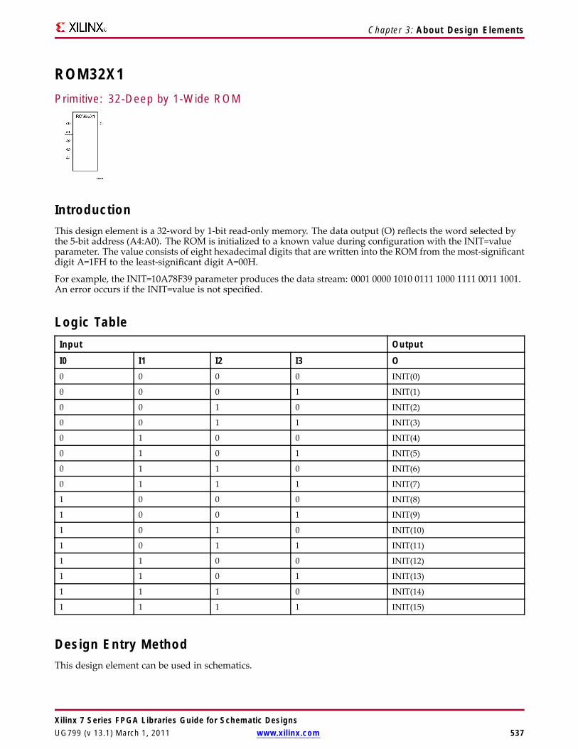
Chapter 3: About Design Elements
ROM32X1Primitive: 32-Deep by 1-Wide ROM
IntroductionThis design element is a 32-word by 1-bit read-only memory. The data output (O) reflects the word selected bythe 5-bit address (A4:A0). The ROM is initialized to a known value during configuration with the INIT=valueparameter. The value consists of eight hexadecimal digits that are written into the ROM from the most-significantdigit A=1FH to the least-significant digit A=00H.
For example, the INIT=10A78F39 parameter produces the data stream: 0001 0000 1010 0111 1000 1111 0011 1001.An error occurs if the INIT=value is not specified.
Logic TableInput Output
I0 I1 I2 I3 O0 0 0 0 INIT(0)
0 0 0 1 INIT(1)
0 0 1 0 INIT(2)
0 0 1 1 INIT(3)
0 1 0 0 INIT(4)
0 1 0 1 INIT(5)
0 1 1 0 INIT(6)
0 1 1 1 INIT(7)
1 0 0 0 INIT(8)
1 0 0 1 INIT(9)
1 0 1 0 INIT(10)
1 0 1 1 INIT(11)
1 1 0 0 INIT(12)
1 1 0 1 INIT(13)
1 1 1 0 INIT(14)
1 1 1 1 INIT(15)
Design Entry MethodThis design element can be used in schematics.
Xilinx 7 Series FPGA Libraries Guide for Schematic DesignsUG799 (v 13.1) March 1, 2011 www.xilinx.com 537

Chapter 3: About Design Elements
Available AttributesAttribute Type Allowed Values Default DescriptionINIT Hexadecimal Any 32-Bit Value All zeros Specifies the contents of the ROM.
For More InformationSee the 7 series FPGA User Documentation (User Guides and Data Sheets).
Xilinx 7 Series FPGA Libraries Guide for Schematic Designs538 www.xilinx.com UG799 (v 13.1) March 1, 2011

Chapter 3: About Design Elements
ROM64X1Primitive: 64-Deep by 1-Wide ROM
IntroductionThis design element is a 64-word by 1-bit read-only memory. The data output (O) reflects the word selected bythe 6-bit address (A5:A0). The ROM is initialized to a known value during configuration with the INIT=valueparameter. The value consists of 16 hexadecimal digits that are written into the ROM from the most-significantdigit A=FH to the least-significant digit A=0H. An error occurs if the INIT=value is not specified.
Logic TableInput Output
I0 I1 I2 I3 O0 0 0 0 INIT(0)
0 0 0 1 INIT(1)
0 0 1 0 INIT(2)
0 0 1 1 INIT(3)
0 1 0 0 INIT(4)
0 1 0 1 INIT(5)
0 1 1 0 INIT(6)
0 1 1 1 INIT(7)
1 0 0 0 INIT(8)
1 0 0 1 INIT(9)
1 0 1 0 INIT(10)
1 0 1 1 INIT(11)
1 1 0 0 INIT(12)
1 1 0 1 INIT(13)
1 1 1 0 INIT(14)
1 1 1 1 INIT(15)
Design Entry MethodThis design element can be used in schematics.
Xilinx 7 Series FPGA Libraries Guide for Schematic DesignsUG799 (v 13.1) March 1, 2011 www.xilinx.com 539
Chapter 3: About Design Elements
Available AttributesAttribute Type Allowed Values Default DescriptionINIT Hexadecimal Any 64-Bit Value All zeros Specifies the contents of the ROM.
For More InformationSee the 7 series FPGA User Documentation (User Guides and Data Sheets).
Xilinx 7 Series FPGA Libraries Guide for Schematic Designs540 www.xilinx.com UG799 (v 13.1) March 1, 2011

Chapter 3: About Design Elements
SOP3Macro: 3–Input Sum of Products
IntroductionThree input Sum of Products (SOP) macros provide common logic functions by OR gating the output of oneAND function with one direct input. Variations of inverting and non-inverting inputs are available.
Design Entry MethodThis design element is only for use in schematics.
For More InformationSee the 7 series FPGA User Documentation (User Guides and Data Sheets).
Xilinx 7 Series FPGA Libraries Guide for Schematic DesignsUG799 (v 13.1) March 1, 2011 www.xilinx.com 541

Chapter 3: About Design Elements
SOP3B1AMacro: 3–Input Sum of Products with One Inverted Input (Option A)
IntroductionThree input Sum of Products (SOP) macros provide common logic functions by OR gating the output of oneAND function with one direct input. Variations of inverting and non-inverting inputs are available.
Design Entry MethodThis design element is only for use in schematics.
For More InformationSee the 7 series FPGA User Documentation (User Guides and Data Sheets).
Xilinx 7 Series FPGA Libraries Guide for Schematic Designs542 www.xilinx.com UG799 (v 13.1) March 1, 2011

Chapter 3: About Design Elements
SOP3B1BMacro: 3–Input Sum of Products with One Inverted Input (Option B)
IntroductionThree input Sum of Products (SOP) macros provide common logic functions by OR gating the output of oneAND function with one direct input. Variations of inverting and non-inverting inputs are available.
Design Entry MethodThis design element is only for use in schematics.
For More InformationSee the 7 series FPGA User Documentation (User Guides and Data Sheets).
Xilinx 7 Series FPGA Libraries Guide for Schematic DesignsUG799 (v 13.1) March 1, 2011 www.xilinx.com 543

Chapter 3: About Design Elements
SOP3B2AMacro: 3–Input Sum of Products with Two Inverted Inputs (Option A)
IntroductionThree input Sum of Products (SOP) macros provide common logic functions by OR gating the output of oneAND function with one direct input. Variations of inverting and non-inverting inputs are available.
Design Entry MethodThis design element is only for use in schematics.
For More InformationSee the 7 series FPGA User Documentation (User Guides and Data Sheets).
Xilinx 7 Series FPGA Libraries Guide for Schematic Designs544 www.xilinx.com UG799 (v 13.1) March 1, 2011

Chapter 3: About Design Elements
SOP3B2BMacro: 3–Input Sum of Products with Two Inverted Inputs (Option B)
IntroductionThree input Sum of Products (SOP) macros provide common logic functions by OR gating the output of oneAND function with one direct input. Variations of inverting and non-inverting inputs are available.
Design Entry MethodThis design element is only for use in schematics.
For More InformationSee the 7 series FPGA User Documentation (User Guides and Data Sheets).
Xilinx 7 Series FPGA Libraries Guide for Schematic DesignsUG799 (v 13.1) March 1, 2011 www.xilinx.com 545

Chapter 3: About Design Elements
SOP3B3Macro: 3–Input Sum of Products with Inverted Inputs
IntroductionThree input Sum of Products (SOP) macros provide common logic functions by OR gating the output of oneAND function with one direct input. Variations of inverting and non-inverting inputs are available.
Design Entry MethodThis design element is only for use in schematics.
For More InformationSee the 7 series FPGA User Documentation (User Guides and Data Sheets).
Xilinx 7 Series FPGA Libraries Guide for Schematic Designs546 www.xilinx.com UG799 (v 13.1) March 1, 2011

Chapter 3: About Design Elements
SOP4Macro: 4–Input Sum of Products
IntroductionFour input Sum of Products (SOP) macros provide common logic functions by OR gating the outputs of twoAND functions. Variations of inverting and non-inverting inputs are available.
Design Entry MethodThis design element is only for use in schematics.
For More InformationSee the 7 series FPGA User Documentation (User Guides and Data Sheets).
Xilinx 7 Series FPGA Libraries Guide for Schematic DesignsUG799 (v 13.1) March 1, 2011 www.xilinx.com 547
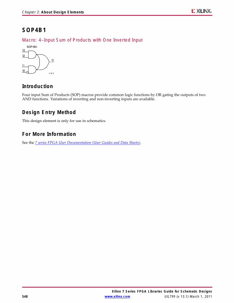
Chapter 3: About Design Elements
SOP4B1Macro: 4–Input Sum of Products with One Inverted Input
IntroductionFour input Sum of Products (SOP) macros provide common logic functions by OR gating the outputs of twoAND functions. Variations of inverting and non-inverting inputs are available.
Design Entry MethodThis design element is only for use in schematics.
For More InformationSee the 7 series FPGA User Documentation (User Guides and Data Sheets).
Xilinx 7 Series FPGA Libraries Guide for Schematic Designs548 www.xilinx.com UG799 (v 13.1) March 1, 2011

Chapter 3: About Design Elements
SOP4B2AMacro: 4–Input Sum of Products with Two Inverted Inputs (Option A)
IntroductionFour input Sum of Products (SOP) macros provide common logic functions by OR gating the outputs of twoAND functions. Variations of inverting and non-inverting inputs are available.
Design Entry MethodThis design element is only for use in schematics.
For More InformationSee the 7 series FPGA User Documentation (User Guides and Data Sheets).
Xilinx 7 Series FPGA Libraries Guide for Schematic DesignsUG799 (v 13.1) March 1, 2011 www.xilinx.com 549

Chapter 3: About Design Elements
SOP4B2BMacro: 4–Input Sum of Products with Two Inverted Inputs (Option B)
IntroductionFour input Sum of Products (SOP) macros provide common logic functions by OR gating the outputs of twoAND functions. Variations of inverting and non-inverting inputs are available.
Design Entry MethodThis design element is only for use in schematics.
For More InformationSee the 7 series FPGA User Documentation (User Guides and Data Sheets).
Xilinx 7 Series FPGA Libraries Guide for Schematic Designs550 www.xilinx.com UG799 (v 13.1) March 1, 2011

Chapter 3: About Design Elements
SOP4B3Macro: 4–Input Sum of Products with Three Inverted Inputs
IntroductionFour input Sum of Products (SOP) macros provide common logic functions by OR gating the outputs of twoAND functions. Variations of inverting and non-inverting inputs are available.
Design Entry MethodThis design element is only for use in schematics.
For More InformationSee the 7 series FPGA User Documentation (User Guides and Data Sheets).
Xilinx 7 Series FPGA Libraries Guide for Schematic DesignsUG799 (v 13.1) March 1, 2011 www.xilinx.com 551

Chapter 3: About Design Elements
SOP4B4Macro: 4–Input Sum of Products with Inverted Inputs
IntroductionFour input Sum of Products (SOP) macros provide common logic functions by OR gating the outputs of twoAND functions. Variations of inverting and non-inverting inputs are available.
Design Entry MethodThis design element is only for use in schematics.
For More InformationSee the 7 series FPGA User Documentation (User Guides and Data Sheets).
Xilinx 7 Series FPGA Libraries Guide for Schematic Designs552 www.xilinx.com UG799 (v 13.1) March 1, 2011

Chapter 3: About Design Elements
SR16CEMacro: 16-Bit Serial-In Parallel-Out Shift Register with Clock Enable and AsynchronousClear
IntroductionThis design element is a shift register with a shift-left serial input (SLI), parallel outputs (Q), and clock enable(CE) and asynchronous clear (CLR) inputs. The (CLR) input, when High, overrides all other inputs and resets thedata outputs (Q) Low. When (CE) is High and (CLR) is Low, the data on the SLI input is loaded into the firstbit of the shift register during the Low-to- High clock (C) transition and appears on the (Q0) output. Duringsubsequent Low-to- High clock transitions, when (CE) is High and (CLR) is Low, data shifts to the next highestbit position as new data is loaded into (Q0) (SLI→Q0, Q0→Q1, Q1→Q2, and so forth). The register ignores clocktransitions when (CE) is Low.
Registers can be cascaded by connecting the last (Q) output of one stage to the SLI input of the next stageand connecting clock, (CE), and (CLR) in parallel.
This register is asynchronously cleared, outputs Low, when power is applied. For FPGA devices, power-onconditions are simulated when global set/reset (GSR) is active. GSR defaults to active-High but can be invertedby adding an inverter in front of the GSR input of the appropriate STARTUP_architecture symbol.
Logic TableInputs Outputs
CLR CE SLI C Q0 Qz : Q11 X X X 0 0
0 0 X X No Change No Change
0 1 SLI ↑ SLI qn-1
z = bit width - 1
qn-1 = state of referenced output one setup time prior to active clock transition
Design Entry MethodThis design element is only for use in schematics.
For More InformationSee the 7 series FPGA User Documentation (User Guides and Data Sheets).
Xilinx 7 Series FPGA Libraries Guide for Schematic DesignsUG799 (v 13.1) March 1, 2011 www.xilinx.com 553

Chapter 3: About Design Elements
SR16CLEMacro: 16-Bit Loadable Serial/Parallel-In Parallel-Out Shift Register with Clock Enableand Asynchronous Clear
IntroductionThis design element is a shift register with a shift-left serial input (SLI), parallel inputs (D), parallel outputs (Q),and three control inputs: clock enable (CE), load enable (L), and asynchronous clear (CLR) . The register ignoresclock transitions when (L) and (CE) are Low. The asynchronous (CLR), when High, overrides all other inputsand resets the data outputs (Q) Low. When (L) is High and (CLR) is Low, data on the Dn -D0 inputs is loadedinto the corresponding Qn -(Q0) bits of the register.
When (CE) is High and (L) and (CLR) are Low, data on the SLI input is loaded into the first bit of the shiftregister during the Low-to-High clock (C) transition and appears on the (Q0) output. During subsequent clocktransitions, when (CE) is High and (L) and (CLR) are Low, the data shifts to the next highest bit position as newdata is loaded into (Q)0 (for example, SLI→Q0, Q0→Q1, and Q1→Q2).
Registers can be cascaded by connecting the last (Q) output of one stage to the SLI input of the next stage andconnecting clock, (CE), (L), and (CLR) inputs in parallel.
This register is asynchronously cleared, outputs Low, when power is applied. For FPGA devices, power-onconditions are simulated when global set/reset (GSR) is active. GSR defaults to active-High but can be invertedby adding an inverter in front of the GSR input of the appropriate STARTUP_architecture symbol.
Logic TableInputs Outputs
CLR L CE SLI Dn : D0 C Q0 Qz : Q11 X X X X X 0 0
0 1 X X Dn : D0 ↑ D0 Dn
0 0 1 SLI X ↑ SLI qn-1
0 0 0 X X X No Change No Change
z = bitwidth -1
qn-1 = state of referenced output one setup time prior to active clock transition
Design Entry MethodThis design element is only for use in schematics.
Xilinx 7 Series FPGA Libraries Guide for Schematic Designs554 www.xilinx.com UG799 (v 13.1) March 1, 2011

Chapter 3: About Design Elements
For More InformationSee the 7 series FPGA User Documentation (User Guides and Data Sheets).
Xilinx 7 Series FPGA Libraries Guide for Schematic DesignsUG799 (v 13.1) March 1, 2011 www.xilinx.com 555

Chapter 3: About Design Elements
SR16CLEDMacro: 16-Bit Shift Register with Clock Enable and Asynchronous Clear
IntroductionThis design element is a shift register with shift-left (SLI) and shift-right (SRI) serial inputs, parallel inputs (D),parallel outputs (Q), and four control inputs: clock enable (CE), load enable (L), shift left/right (LEFT), andasynchronous clear (CLR). The register ignores clock transitions when (CE) and (L) are Low. The asynchronousclear, when High, overrides all other inputs and resets the data outputs (Qn) Low.
When (L) is High and (CLR) is Low, the data on the (D) inputs is loaded into the corresponding (Q) bits of theregister. When (CE) is High and (L) and (CLR) are Low, data is shifted right or left, depending on the state of theLEFT input. If LEFT is High, data on the SLI is loaded into (Q0) during the Low-to-High clock transition andshifted left (for example, to Q1 or Q2) during subsequent clock transitions. If LEFT is Low, data on the SRI isloaded into the last (Q) output during the Low-to-High clock transition and shifted right during subsequentclock transitions. The logic tables indicate the state of the (Q) outputs under all input conditions.
This register is asynchronously cleared, outputs Low, when power is applied. For FPGA devices, power-onconditions are simulated when global set/reset (GSR) is active. GSR defaults to active-High but can be invertedby adding an inverter in front of the GSR input of the appropriate STARTUP_architecture symbol.
Logic TableInputs Outputs
CLR L CE LEFT SLI SRID15 :D0 C Q0 Q15
Q14 :Q1
1 X X X X X X X 0 0 0
0 1 X X X X D15 : D0 ↑ D0 D15 Dn
0 0 0 X X X X X NoChange
NoChange
NoChange
0 0 1 1 SLI X X ↑ SLI q14 qn-1
0 0 1 0 X SRI X ↑ q1 SRI qn+1
qn-1 or qn+1 = state of referenced output one setup time prior to active clock transition.
Design Entry MethodThis design element is only for use in schematics.
Xilinx 7 Series FPGA Libraries Guide for Schematic Designs556 www.xilinx.com UG799 (v 13.1) March 1, 2011
Chapter 3: About Design Elements
For More InformationSee the 7 series FPGA User Documentation (User Guides and Data Sheets).
Xilinx 7 Series FPGA Libraries Guide for Schematic DesignsUG799 (v 13.1) March 1, 2011 www.xilinx.com 557

Chapter 3: About Design Elements
SR16REMacro: 16-Bit Serial-In Parallel-Out Shift Register with Clock Enable and SynchronousReset
IntroductionThis design element is a shift register with shift-left serial input (SLI), parallel outputs (Qn), clock enable (CE),and synchronous reset (R) inputs. The R input, when High, overrides all other inputs during the Low-to-Highclock (C) transition and resets the data outputs (Q) Low.
When (CE) is High and (R) is Low, the data on the (SLI) is loaded into the first bit of the shift register duringthe Low-to-High clock (C) transition and appears on the (Q0) output. During subsequent Low-to-High clocktransitions, when (CE) is High and R is Low, data shifts to the next highest bit position as new data is loaded into(Q0) (for example, SLI→Q0, Q0→Q1, and Q1→Q2). The register ignores clock transitions when (CE) is Low.
Registers can be cascaded by connecting the last (Q) output of one stage to the SLI input of the next stage andconnecting clock, (CE), and (R) in parallel.
This register is asynchronously cleared, outputs Low, when power is applied. For FPGA devices, power-onconditions are simulated when global set/reset (GSR) is active. GSR defaults to active-High but can be invertedby adding an inverter in front of the GSR input of the appropriate STARTUP_architecture symbol.
Logic TableInputs Outputs
R CE SLI C Q0 Qz : Q11 X X ↑ 0 0
0 0 X X No Change No Change
0 1 SLI ↑ SLI qn-1
z = bitwidth -1
qn-1 = state of referenced output one setup time prior to active clock transition
Design Entry MethodThis design element is only for use in schematics.
For More InformationSee the 7 series FPGA User Documentation (User Guides and Data Sheets).
Xilinx 7 Series FPGA Libraries Guide for Schematic Designs558 www.xilinx.com UG799 (v 13.1) March 1, 2011
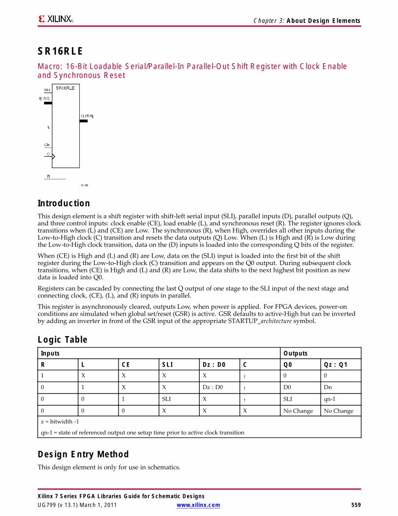
Chapter 3: About Design Elements
SR16RLEMacro: 16-Bit Loadable Serial/Parallel-In Parallel-Out Shift Register with Clock Enableand Synchronous Reset
IntroductionThis design element is a shift register with shift-left serial input (SLI), parallel inputs (D), parallel outputs (Q),and three control inputs: clock enable (CE), load enable (L), and synchronous reset (R). The register ignores clocktransitions when (L) and (CE) are Low. The synchronous (R), when High, overrides all other inputs during theLow-to-High clock (C) transition and resets the data outputs (Q) Low. When (L) is High and (R) is Low duringthe Low-to-High clock transition, data on the (D) inputs is loaded into the corresponding Q bits of the register.
When (CE) is High and (L) and (R) are Low, data on the (SLI) input is loaded into the first bit of the shiftregister during the Low-to-High clock (C) transition and appears on the Q0 output. During subsequent clocktransitions, when (CE) is High and (L) and (R) are Low, the data shifts to the next highest bit position as newdata is loaded into Q0.
Registers can be cascaded by connecting the last Q output of one stage to the SLI input of the next stage andconnecting clock, (CE), (L), and (R) inputs in parallel.
This register is asynchronously cleared, outputs Low, when power is applied. For FPGA devices, power-onconditions are simulated when global set/reset (GSR) is active. GSR defaults to active-High but can be invertedby adding an inverter in front of the GSR input of the appropriate STARTUP_architecture symbol.
Logic TableInputs Outputs
R L CE SLI Dz : D0 C Q0 Qz : Q11 X X X X ↑ 0 0
0 1 X X Dz : D0 ↑ D0 Dn
0 0 1 SLI X ↑ SLI qn-1
0 0 0 X X X No Change No Change
z = bitwidth -1
qn-1 = state of referenced output one setup time prior to active clock transition
Design Entry MethodThis design element is only for use in schematics.
Xilinx 7 Series FPGA Libraries Guide for Schematic DesignsUG799 (v 13.1) March 1, 2011 www.xilinx.com 559

Chapter 3: About Design Elements
For More InformationSee the 7 series FPGA User Documentation (User Guides and Data Sheets).
Xilinx 7 Series FPGA Libraries Guide for Schematic Designs560 www.xilinx.com UG799 (v 13.1) March 1, 2011
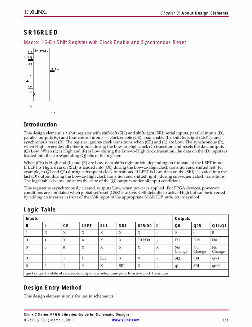
Chapter 3: About Design Elements
SR16RLEDMacro: 16-Bit Shift Register with Clock Enable and Synchronous Reset
IntroductionThis design element is a shift register with shift-left (SLI) and shift-right (SRI) serial inputs, parallel inputs (D),parallel outputs (Q) and four control inputs — clock enable (CE), load enable (L), shift left/right (LEFT), andsynchronous reset (R). The register ignores clock transitions when (CE) and (L) are Low. The synchronous (R),when High, overrides all other inputs during the Low-to-High clock (C) transition and resets the data outputs(Q) Low. When (L) is High and (R) is Low during the Low-to-High clock transition, the data on the (D) inputs isloaded into the corresponding (Q) bits of the register.
When (CE) is High and (L) and (R) are Low, data shifts right or left, depending on the state of the LEFT input.If LEFT is High, data on (SLI) is loaded into (Q0) during the Low-to-High clock transition and shifted left (forexample, to Q1 and Q2) during subsequent clock transitions. If LEFT is Low, data on the (SRI) is loaded into thelast (Q) output during the Low-to-High clock transition and shifted right ) during subsequent clock transitions.The logic tables below indicates the state of the (Q) outputs under all input conditions.
This register is asynchronously cleared, outputs Low, when power is applied. For FPGA devices, power-onconditions are simulated when global set/reset (GSR) is active. GSR defaults to active-High but can be invertedby adding an inverter in front of the GSR input of the appropriate STARTUP_architecture symbol.
Logic TableInputs Outputs
R L CE LEFT SLI SRI D15:D0 C Q0 Q15 Q14:Q11 X X X X X X ↑ 0 0 0
0 1 X X X X D15:D0 ↓ D0 D15 Dn
0 0 0 X X X X X NoChange
NoChange
NoChange
0 0 1 1 SLI X X ↑ SLI q14 qn-1
0 0 1 0 X SRI X ↓ q1 SRI qn+1
qn-1 or qn+1 = state of referenced output one setup time prior to active clock transition
Design Entry MethodThis design element is only for use in schematics.
Xilinx 7 Series FPGA Libraries Guide for Schematic DesignsUG799 (v 13.1) March 1, 2011 www.xilinx.com 561

Chapter 3: About Design Elements
For More InformationSee the 7 series FPGA User Documentation (User Guides and Data Sheets).
Xilinx 7 Series FPGA Libraries Guide for Schematic Designs562 www.xilinx.com UG799 (v 13.1) March 1, 2011

Chapter 3: About Design Elements
SR4CEMacro: 4-Bit Serial-In Parallel-Out Shift Register with Clock Enable and AsynchronousClear
IntroductionThis design element is a shift register with a shift-left serial input (SLI), parallel outputs (Q), and clock enable(CE) and asynchronous clear (CLR) inputs. The (CLR) input, when High, overrides all other inputs and resets thedata outputs (Q) Low. When (CE) is High and (CLR) is Low, the data on the SLI input is loaded into the firstbit of the shift register during the Low-to- High clock (C) transition and appears on the (Q0) output. Duringsubsequent Low-to- High clock transitions, when (CE) is High and (CLR) is Low, data shifts to the next highestbit position as new data is loaded into (Q0) (SLI→Q0, Q0→Q1, Q1→Q2, and so forth). The register ignores clocktransitions when (CE) is Low.
Registers can be cascaded by connecting the last (Q) output of one stage to the SLI input of the next stageand connecting clock, (CE), and (CLR) in parallel.
This register is asynchronously cleared, outputs Low, when power is applied. For FPGA devices, power-onconditions are simulated when global set/reset (GSR) is active. GSR defaults to active-High but can be invertedby adding an inverter in front of the GSR input of the appropriate STARTUP_architecture symbol.
Logic TableInputs Outputs
CLR CE SLI C Q0 Qz : Q11 X X X 0 0
0 0 X X No Change No Change
0 1 SLI ↑ SLI qn-1
z = bit width - 1
qn-1 = state of referenced output one setup time prior to active clock transition
Design Entry MethodThis design element is only for use in schematics.
For More InformationSee the 7 series FPGA User Documentation (User Guides and Data Sheets).
Xilinx 7 Series FPGA Libraries Guide for Schematic DesignsUG799 (v 13.1) March 1, 2011 www.xilinx.com 563

Chapter 3: About Design Elements
SR4CLEMacro: 4-Bit Loadable Serial/Parallel-In Parallel-Out Shift Register with Clock Enableand Asynchronous Clear
IntroductionThis design element is a shift register with a shift-left serial input (SLI), parallel inputs (D), parallel outputs (Q),and three control inputs: clock enable (CE), load enable (L), and asynchronous clear (CLR) . The register ignoresclock transitions when (L) and (CE) are Low. The asynchronous (CLR), when High, overrides all other inputsand resets the data outputs (Q) Low. When (L) is High and (CLR) is Low, data on the Dn -D0 inputs is loadedinto the corresponding Qn -(Q0) bits of the register.
When (CE) is High and (L) and (CLR) are Low, data on the SLI input is loaded into the first bit of the shiftregister during the Low-to-High clock (C) transition and appears on the (Q0) output. During subsequent clocktransitions, when (CE) is High and (L) and (CLR) are Low, the data shifts to the next highest bit position as newdata is loaded into (Q)0 (for example, SLI→Q0, Q0→Q1, and Q1→Q2).
Registers can be cascaded by connecting the last (Q) output of one stage to the SLI input of the next stage andconnecting clock, (CE), (L), and (CLR) inputs in parallel.
This register is asynchronously cleared, outputs Low, when power is applied. For FPGA devices, power-onconditions are simulated when global set/reset (GSR) is active. GSR defaults to active-High but can be invertedby adding an inverter in front of the GSR input of the appropriate STARTUP_architecture symbol.
Logic TableInputs Outputs
CLR L CE SLI Dn : D0 C Q0 Qz : Q11 X X X X X 0 0
0 1 X X Dn : D0 ↑ D0 Dn
0 0 1 SLI X ↑ SLI qn-1
0 0 0 X X X No Change No Change
z = bitwidth -1
qn-1 = state of referenced output one setup time prior to active clock transition
Xilinx 7 Series FPGA Libraries Guide for Schematic Designs564 www.xilinx.com UG799 (v 13.1) March 1, 2011

Chapter 3: About Design Elements
Design Entry MethodThis design element is only for use in schematics.
For More InformationSee the 7 series FPGA User Documentation (User Guides and Data Sheets).
Xilinx 7 Series FPGA Libraries Guide for Schematic DesignsUG799 (v 13.1) March 1, 2011 www.xilinx.com 565

Chapter 3: About Design Elements
SR4CLEDMacro: 4-Bit Shift Register with Clock Enable and Asynchronous Clear
IntroductionThis design element is a shift register with shift-left (SLI) and shift-right (SRI) serial inputs, parallel inputs (D),parallel outputs (Q), and four control inputs: clock enable (CE), load enable (L), shift left/right (LEFT), andasynchronous clear (CLR). The register ignores clock transitions when (CE) and (L) are Low. The asynchronousclear, when High, overrides all other inputs and resets the data outputs (Qn) Low.
When (L) is High and (CLR) is Low, the data on the (D) inputs is loaded into the corresponding (Q) bits of theregister. When (CE) is High and (L) and (CLR) are Low, data is shifted right or left, depending on the state of theLEFT input. If LEFT is High, data on the SLI is loaded into (Q0) during the Low-to-High clock transition andshifted left (for example, to Q1 or Q2) during subsequent clock transitions. If LEFT is Low, data on the SRI isloaded into the last (Q) output during the Low-to-High clock transition and shifted right during subsequentclock transitions. The logic tables indicate the state of the (Q) outputs under all input conditions.
This register is asynchronously cleared, outputs Low, when power is applied. For FPGA devices, power-onconditions are simulated when global set/reset (GSR) is active. GSR defaults to active-High but can be invertedby adding an inverter in front of the GSR input of the appropriate STARTUP_architecture symbol.
Logic TableInputs Outputs
CLR L CE LEFT SLI SRI D3 : D0 C Q0 Q3 Q2 : Q11 X X X X X X X 0 0 0
0 1 X X X X D3– D0 ↑ D0 D3 Dn
0 0 0 X X X X X NoChange
NoChange
NoChange
0 0 1 1 SLI X X ↑ SLI q2 qn-1
0 0 1 0 X SRI X ↑ q1 SRI qn+1
qn-1 and qn+1 = state of referenced output one setup time prior to active clock transition.
Design Entry MethodThis design element is only for use in schematics.
Xilinx 7 Series FPGA Libraries Guide for Schematic Designs566 www.xilinx.com UG799 (v 13.1) March 1, 2011

Chapter 3: About Design Elements
For More InformationSee the 7 series FPGA User Documentation (User Guides and Data Sheets).
Xilinx 7 Series FPGA Libraries Guide for Schematic DesignsUG799 (v 13.1) March 1, 2011 www.xilinx.com 567

Chapter 3: About Design Elements
SR4REMacro: 4-Bit Serial-In Parallel-Out Shift Register with Clock Enable and SynchronousReset
IntroductionThis design element is a shift register with shift-left serial input (SLI), parallel outputs (Qn), clock enable (CE),and synchronous reset (R) inputs. The R input, when High, overrides all other inputs during the Low-to-Highclock (C) transition and resets the data outputs (Q) Low.
When (CE) is High and (R) is Low, the data on the (SLI) is loaded into the first bit of the shift register duringthe Low-to-High clock (C) transition and appears on the (Q0) output. During subsequent Low-to-High clocktransitions, when (CE) is High and R is Low, data shifts to the next highest bit position as new data is loaded into(Q0) (for example, SLI→Q0, Q0→Q1, and Q1→Q2). The register ignores clock transitions when (CE) is Low.
Registers can be cascaded by connecting the last (Q) output of one stage to the SLI input of the next stage andconnecting clock, (CE), and (R) in parallel.
This register is asynchronously cleared, outputs Low, when power is applied. For FPGA devices, power-onconditions are simulated when global set/reset (GSR) is active. GSR defaults to active-High but can be invertedby adding an inverter in front of the GSR input of the appropriate STARTUP_architecture symbol.
Logic TableInputs Outputs
R CE SLI C Q0 Qz : Q11 X X ↑ 0 0
0 0 X X No Change No Change
0 1 SLI ↑ SLI qn-1
z = bitwidth -1
qn-1 = state of referenced output one setup time prior to active clock transition
Design Entry MethodThis design element is only for use in schematics.
For More InformationSee the 7 series FPGA User Documentation (User Guides and Data Sheets).
Xilinx 7 Series FPGA Libraries Guide for Schematic Designs568 www.xilinx.com UG799 (v 13.1) March 1, 2011

Chapter 3: About Design Elements
SR4RLEMacro: 4-Bit Loadable Serial/Parallel-In Parallel-Out Shift Register with Clock Enableand Synchronous Reset
IntroductionThis design element is a shift register with shift-left serial input (SLI), parallel inputs (D), parallel outputs (Q),and three control inputs: clock enable (CE), load enable (L), and synchronous reset (R). The register ignores clocktransitions when (L) and (CE) are Low. The synchronous (R), when High, overrides all other inputs during theLow-to-High clock (C) transition and resets the data outputs (Q) Low. When (L) is High and (R) is Low duringthe Low-to-High clock transition, data on the (D) inputs is loaded into the corresponding Q bits of the register.
When (CE) is High and (L) and (R) are Low, data on the (SLI) input is loaded into the first bit of the shiftregister during the Low-to-High clock (C) transition and appears on the Q0 output. During subsequent clocktransitions, when (CE) is High and (L) and (R) are Low, the data shifts to the next highest bit position as newdata is loaded into Q0.
Registers can be cascaded by connecting the last Q output of one stage to the SLI input of the next stage andconnecting clock, (CE), (L), and (R) inputs in parallel.
This register is asynchronously cleared, outputs Low, when power is applied. For FPGA devices, power-onconditions are simulated when global set/reset (GSR) is active. GSR defaults to active-High but can be invertedby adding an inverter in front of the GSR input of the appropriate STARTUP_architecture symbol.
Logic TableInputs Outputs
R L CE SLI Dz : D0 C Q0 Qz : Q11 X X X X ↑ 0 0
0 1 X X Dz : D0 ↑ D0 Dn
0 0 1 SLI X ↑ SLI qn-1
0 0 0 X X X No Change No Change
z = bitwidth -1
qn-1 = state of referenced output one setup time prior to active clock transition
Xilinx 7 Series FPGA Libraries Guide for Schematic DesignsUG799 (v 13.1) March 1, 2011 www.xilinx.com 569

Chapter 3: About Design Elements
Design Entry MethodThis design element is only for use in schematics.
For More InformationSee the 7 series FPGA User Documentation (User Guides and Data Sheets).
Xilinx 7 Series FPGA Libraries Guide for Schematic Designs570 www.xilinx.com UG799 (v 13.1) March 1, 2011

Chapter 3: About Design Elements
SR4RLEDMacro: 4-Bit Shift Register with Clock Enable and Synchronous Reset
IntroductionThis design element is a shift register with shift-left (SLI) and shift-right (SRI) serial inputs, parallel inputs (D),parallel outputs (Q) and four control inputs — clock enable (CE), load enable (L), shift left/right (LEFT), andsynchronous reset (R). The register ignores clock transitions when (CE) and (L) are Low. The synchronous (R),when High, overrides all other inputs during the Low-to-High clock (C) transition and resets the data outputs(Q) Low. When (L) is High and (R) is Low during the Low-to-High clock transition, the data on the (D) inputs isloaded into the corresponding (Q) bits of the register.
When (CE) is High and (L) and (R) are Low, data shifts right or left, depending on the state of the LEFT input.If LEFT is High, data on (SLI) is loaded into (Q0) during the Low-to-High clock transition and shifted left (forexample, to Q1 and Q2) during subsequent clock transitions. If LEFT is Low, data on the (SRI) is loaded into thelast (Q) output during the Low-to-High clock transition and shifted right ) during subsequent clock transitions.The logic tables below indicates the state of the (Q) outputs under all input conditions.
This register is asynchronously cleared, outputs Low, when power is applied. For FPGA devices, power-onconditions are simulated when global set/reset (GSR) is active. GSR defaults to active-High but can be invertedby adding an inverter in front of the GSR input of the appropriate STARTUP_architecture symbol.
Logic TableInputs Outputs
R L CE LEFT SLI SRI D3 : D0 C Q0 Q3 Q2 : Q11 X X X X X X ↑ 0 0 0
0 1 X X X X D3 : D0 ↑ D0 D3 Dn
0 0 0 X X X X X NoChange
NoChange
NoChange
0 0 1 1 SLI X X ↑ SLI q2 qn-1
0 0 1 0 X SRI X ↑ q1 SRI qn+1
qn-1 or qn+1 = state of referenced output one setup time prior to active clock transition
Xilinx 7 Series FPGA Libraries Guide for Schematic DesignsUG799 (v 13.1) March 1, 2011 www.xilinx.com 571

Chapter 3: About Design Elements
Design Entry MethodThis design element is only for use in schematics.
For More InformationSee the 7 series FPGA User Documentation (User Guides and Data Sheets).
Xilinx 7 Series FPGA Libraries Guide for Schematic Designs572 www.xilinx.com UG799 (v 13.1) March 1, 2011

Chapter 3: About Design Elements
SR8CEMacro: 8-Bit Serial-In Parallel-Out Shift Register with Clock Enable and AsynchronousClear
IntroductionThis design element is a shift register with a shift-left serial input (SLI), parallel outputs (Q), and clock enable(CE) and asynchronous clear (CLR) inputs. The (CLR) input, when High, overrides all other inputs and resets thedata outputs (Q) Low. When (CE) is High and (CLR) is Low, the data on the SLI input is loaded into the firstbit of the shift register during the Low-to- High clock (C) transition and appears on the (Q0) output. Duringsubsequent Low-to- High clock transitions, when (CE) is High and (CLR) is Low, data shifts to the next highestbit position as new data is loaded into (Q0) (SLI→Q0, Q0→Q1, Q1→Q2, and so forth). The register ignores clocktransitions when (CE) is Low.
Registers can be cascaded by connecting the last (Q) output of one stage to the SLI input of the next stageand connecting clock, (CE), and (CLR) in parallel.
This register is asynchronously cleared, outputs Low, when power is applied. For FPGA devices, power-onconditions are simulated when global set/reset (GSR) is active. GSR defaults to active-High but can be invertedby adding an inverter in front of the GSR input of the appropriate STARTUP_architecture symbol.
Logic TableInputs Outputs
CLR CE SLI C Q0 Qz : Q11 X X X 0 0
0 0 X X No Change No Change
0 1 SLI ↑ SLI qn-1
z = bit width - 1
qn-1 = state of referenced output one setup time prior to active clock transition
Design Entry MethodThis design element is only for use in schematics.
For More InformationSee the 7 series FPGA User Documentation (User Guides and Data Sheets).
Xilinx 7 Series FPGA Libraries Guide for Schematic DesignsUG799 (v 13.1) March 1, 2011 www.xilinx.com 573
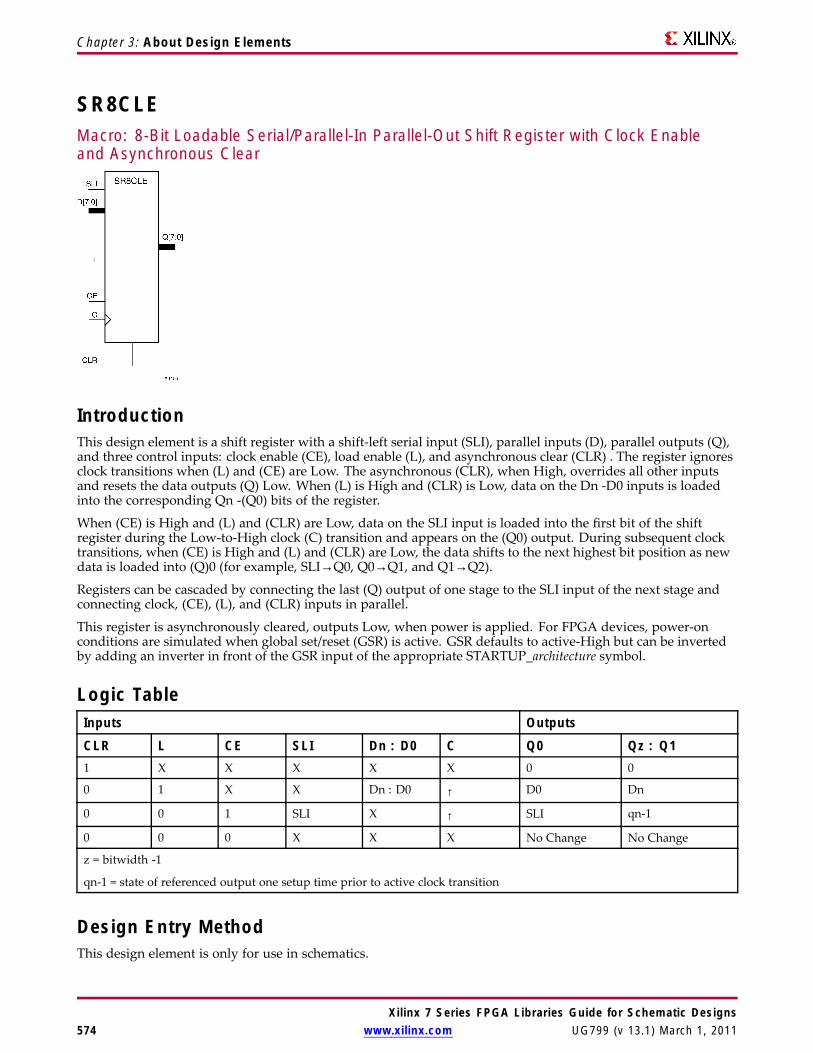
Chapter 3: About Design Elements
SR8CLEMacro: 8-Bit Loadable Serial/Parallel-In Parallel-Out Shift Register with Clock Enableand Asynchronous Clear
IntroductionThis design element is a shift register with a shift-left serial input (SLI), parallel inputs (D), parallel outputs (Q),and three control inputs: clock enable (CE), load enable (L), and asynchronous clear (CLR) . The register ignoresclock transitions when (L) and (CE) are Low. The asynchronous (CLR), when High, overrides all other inputsand resets the data outputs (Q) Low. When (L) is High and (CLR) is Low, data on the Dn -D0 inputs is loadedinto the corresponding Qn -(Q0) bits of the register.
When (CE) is High and (L) and (CLR) are Low, data on the SLI input is loaded into the first bit of the shiftregister during the Low-to-High clock (C) transition and appears on the (Q0) output. During subsequent clocktransitions, when (CE) is High and (L) and (CLR) are Low, the data shifts to the next highest bit position as newdata is loaded into (Q)0 (for example, SLI→Q0, Q0→Q1, and Q1→Q2).
Registers can be cascaded by connecting the last (Q) output of one stage to the SLI input of the next stage andconnecting clock, (CE), (L), and (CLR) inputs in parallel.
This register is asynchronously cleared, outputs Low, when power is applied. For FPGA devices, power-onconditions are simulated when global set/reset (GSR) is active. GSR defaults to active-High but can be invertedby adding an inverter in front of the GSR input of the appropriate STARTUP_architecture symbol.
Logic TableInputs Outputs
CLR L CE SLI Dn : D0 C Q0 Qz : Q11 X X X X X 0 0
0 1 X X Dn : D0 ↑ D0 Dn
0 0 1 SLI X ↑ SLI qn-1
0 0 0 X X X No Change No Change
z = bitwidth -1
qn-1 = state of referenced output one setup time prior to active clock transition
Design Entry MethodThis design element is only for use in schematics.
Xilinx 7 Series FPGA Libraries Guide for Schematic Designs574 www.xilinx.com UG799 (v 13.1) March 1, 2011

Chapter 3: About Design Elements
For More InformationSee the 7 series FPGA User Documentation (User Guides and Data Sheets).
Xilinx 7 Series FPGA Libraries Guide for Schematic DesignsUG799 (v 13.1) March 1, 2011 www.xilinx.com 575

Chapter 3: About Design Elements
SR8CLEDMacro: 8-Bit Shift Register with Clock Enable and Asynchronous Clear
IntroductionThis design element is a shift register with shift-left (SLI) and shift-right (SRI) serial inputs, parallel inputs (D),parallel outputs (Q), and four control inputs: clock enable (CE), load enable (L), shift left/right (LEFT), andasynchronous clear (CLR). The register ignores clock transitions when (CE) and (L) are Low. The asynchronousclear, when High, overrides all other inputs and resets the data outputs (Qn) Low.
When (L) is High and (CLR) is Low, the data on the (D) inputs is loaded into the corresponding (Q) bits of theregister. When (CE) is High and (L) and (CLR) are Low, data is shifted right or left, depending on the state of theLEFT input. If LEFT is High, data on the SLI is loaded into (Q0) during the Low-to-High clock transition andshifted left (for example, to Q1 or Q2) during subsequent clock transitions. If LEFT is Low, data on the SRI isloaded into the last (Q) output during the Low-to-High clock transition and shifted right during subsequentclock transitions. The logic tables indicate the state of the (Q) outputs under all input conditions.
This register is asynchronously cleared, outputs Low, when power is applied. For FPGA devices, power-onconditions are simulated when global set/reset (GSR) is active. GSR defaults to active-High but can be invertedby adding an inverter in front of the GSR input of the appropriate STARTUP_architecture symbol.
Logic TableInputs Outputs
CLR L CE LEFT SLI SRI D7 : D0 C Q0 Q7 Q6 : Q11 X X X X X X X 0 0 0
0 1 X X X X D7 : D0 ↑ D0 D7 Dn
0 0 0 X X X X X NoChange
NoChange
NoChange
0 0 1 1 SLI X X ↑ SLI q6 qn-1
0 0 1 0 X SRI X ↑ q1 SRI qn+1
qn-1 or qn+1 = state of referenced output one setup time prior to active clock transition.
Design Entry MethodThis design element is only for use in schematics.
Xilinx 7 Series FPGA Libraries Guide for Schematic Designs576 www.xilinx.com UG799 (v 13.1) March 1, 2011

Chapter 3: About Design Elements
For More InformationSee the 7 series FPGA User Documentation (User Guides and Data Sheets).
Xilinx 7 Series FPGA Libraries Guide for Schematic DesignsUG799 (v 13.1) March 1, 2011 www.xilinx.com 577
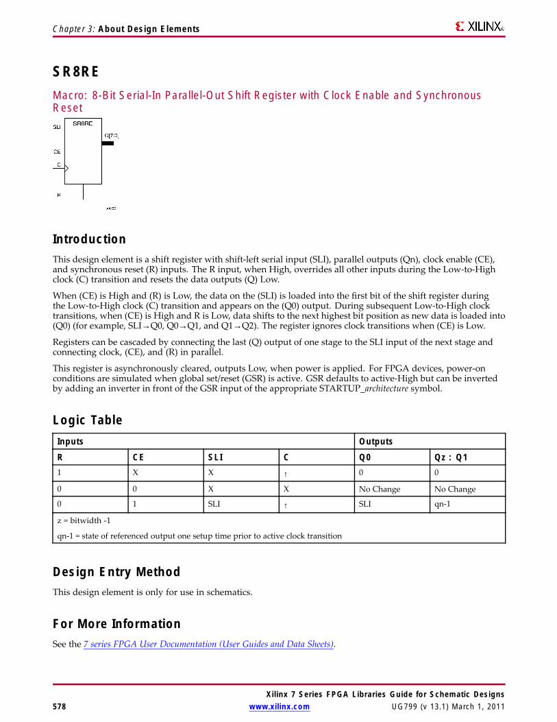
Chapter 3: About Design Elements
SR8REMacro: 8-Bit Serial-In Parallel-Out Shift Register with Clock Enable and SynchronousReset
IntroductionThis design element is a shift register with shift-left serial input (SLI), parallel outputs (Qn), clock enable (CE),and synchronous reset (R) inputs. The R input, when High, overrides all other inputs during the Low-to-Highclock (C) transition and resets the data outputs (Q) Low.
When (CE) is High and (R) is Low, the data on the (SLI) is loaded into the first bit of the shift register duringthe Low-to-High clock (C) transition and appears on the (Q0) output. During subsequent Low-to-High clocktransitions, when (CE) is High and R is Low, data shifts to the next highest bit position as new data is loaded into(Q0) (for example, SLI→Q0, Q0→Q1, and Q1→Q2). The register ignores clock transitions when (CE) is Low.
Registers can be cascaded by connecting the last (Q) output of one stage to the SLI input of the next stage andconnecting clock, (CE), and (R) in parallel.
This register is asynchronously cleared, outputs Low, when power is applied. For FPGA devices, power-onconditions are simulated when global set/reset (GSR) is active. GSR defaults to active-High but can be invertedby adding an inverter in front of the GSR input of the appropriate STARTUP_architecture symbol.
Logic TableInputs Outputs
R CE SLI C Q0 Qz : Q11 X X ↑ 0 0
0 0 X X No Change No Change
0 1 SLI ↑ SLI qn-1
z = bitwidth -1
qn-1 = state of referenced output one setup time prior to active clock transition
Design Entry MethodThis design element is only for use in schematics.
For More InformationSee the 7 series FPGA User Documentation (User Guides and Data Sheets).
Xilinx 7 Series FPGA Libraries Guide for Schematic Designs578 www.xilinx.com UG799 (v 13.1) March 1, 2011

Chapter 3: About Design Elements
SR8RLEMacro: 8-Bit Loadable Serial/Parallel-In Parallel-Out Shift Register with Clock Enableand Synchronous Reset
IntroductionThis design element is a shift register with shift-left serial input (SLI), parallel inputs (D), parallel outputs (Q),and three control inputs: clock enable (CE), load enable (L), and synchronous reset (R). The register ignores clocktransitions when (L) and (CE) are Low. The synchronous (R), when High, overrides all other inputs during theLow-to-High clock (C) transition and resets the data outputs (Q) Low. When (L) is High and (R) is Low duringthe Low-to-High clock transition, data on the (D) inputs is loaded into the corresponding Q bits of the register.
When (CE) is High and (L) and (R) are Low, data on the (SLI) input is loaded into the first bit of the shiftregister during the Low-to-High clock (C) transition and appears on the Q0 output. During subsequent clocktransitions, when (CE) is High and (L) and (R) are Low, the data shifts to the next highest bit position as newdata is loaded into Q0.
Registers can be cascaded by connecting the last Q output of one stage to the SLI input of the next stage andconnecting clock, (CE), (L), and (R) inputs in parallel.
This register is asynchronously cleared, outputs Low, when power is applied. For FPGA devices, power-onconditions are simulated when global set/reset (GSR) is active. GSR defaults to active-High but can be invertedby adding an inverter in front of the GSR input of the appropriate STARTUP_architecture symbol.
Logic TableInputs Outputs
R L CE SLI Dz : D0 C Q0 Qz : Q11 X X X X ↑ 0 0
0 1 X X Dz : D0 ↑ D0 Dn
0 0 1 SLI X ↑ SLI qn-1
0 0 0 X X X No Change No Change
z = bitwidth -1
qn-1 = state of referenced output one setup time prior to active clock transition
Design Entry MethodThis design element is only for use in schematics.
Xilinx 7 Series FPGA Libraries Guide for Schematic DesignsUG799 (v 13.1) March 1, 2011 www.xilinx.com 579

Chapter 3: About Design Elements
For More InformationSee the 7 series FPGA User Documentation (User Guides and Data Sheets).
Xilinx 7 Series FPGA Libraries Guide for Schematic Designs580 www.xilinx.com UG799 (v 13.1) March 1, 2011

Chapter 3: About Design Elements
SR8RLEDMacro: 8-Bit Shift Register with Clock Enable and Synchronous Reset
IntroductionThis design element is a shift register with shift-left (SLI) and shift-right (SRI) serial inputs, parallel inputs (D),parallel outputs (Q) and four control inputs — clock enable (CE), load enable (L), shift left/right (LEFT), andsynchronous reset (R). The register ignores clock transitions when (CE) and (L) are Low. The synchronous (R),when High, overrides all other inputs during the Low-to-High clock (C) transition and resets the data outputs(Q) Low. When (L) is High and (R) is Low during the Low-to-High clock transition, the data on the (D) inputs isloaded into the corresponding (Q) bits of the register.
When (CE) is High and (L) and (R) are Low, data shifts right or left, depending on the state of the LEFT input.If LEFT is High, data on (SLI) is loaded into (Q0) during the Low-to-High clock transition and shifted left (forexample, to Q1 and Q2) during subsequent clock transitions. If LEFT is Low, data on the (SRI) is loaded into thelast (Q) output during the Low-to-High clock transition and shifted right ) during subsequent clock transitions.The logic tables below indicates the state of the (Q) outputs under all input conditions.
This register is asynchronously cleared, outputs Low, when power is applied. For FPGA devices, power-onconditions are simulated when global set/reset (GSR) is active. GSR defaults to active-High but can be invertedby adding an inverter in front of the GSR input of the appropriate STARTUP_architecture symbol.
Logic TableInputs Outputs
R L CE LEFT SLI SRI D7 : D0 C Q0 Q7 Q6 : Q11 X X X X X X ↑ 0 0 0
0 1 X X X X D7 : D0 ↓ D0 D7 Dn
0 0 0 X X X X X NoChange
NoChange
NoChange
0 0 1 1 SLI X X ↑ SLI q6 qn-1
0 0 1 0 X SRI X ↓ q1 SRI qn+1
qn-1 or qn+1 = state of referenced output one setup time prior to active clock transition
Design Entry MethodThis design element is only for use in schematics.
Xilinx 7 Series FPGA Libraries Guide for Schematic DesignsUG799 (v 13.1) March 1, 2011 www.xilinx.com 581
Chapter 3: About Design Elements
For More InformationSee the 7 series FPGA User Documentation (User Guides and Data Sheets).
Xilinx 7 Series FPGA Libraries Guide for Schematic Designs582 www.xilinx.com UG799 (v 13.1) March 1, 2011

Chapter 3: About Design Elements
SRL16Primitive: 16-Bit Shift Register Look-Up Table (LUT)
IntroductionThis design element is a shift register look-up table (LUT). The inputs A3, A2, A1, and A0 select the outputlength of the shift register.
The shift register can be of a fixed, static length or it can be dynamically adjusted.• To create a fixed-length shift register -Drive the A3 through A0 inputs with static values. The length of
the shift register can vary from 1 bit to 16 bits, as determined by the following formula: Length = (8 x A3)+(4 x A2) + (2 x A1) + A0 +1 If A3, A2, A1, and A0 are all zeros (0000), the shift register is one bit long. Ifthey are all ones (1111), it is 16 bits long.
• To change the length of the shift register dynamically -Change the values driving the A3 through A0inputs. For example, if A2, A1, and A0 are all ones (111) and A3 toggles between a one (1) and a zero (0), thelength of the shift register changes from 16 bits to 8 bits. Internally, the length of the shift register is always 16bits and the input lines A3 through A0 select which of the 16 bits reach the output.
The shift register LUT contents are initialized by assigning a four-digit hexadecimal number to an INIT attribute.The first, or the left-most, hexadecimal digit is the most significant bit. If an INIT value is not specified, it defaultsto a value of four zeros (0000) so that the shift register LUT is cleared during configuration.
The data (D) is loaded into the first bit of the shift register during the Low-to-High clock (CLK) transition. Duringsubsequent Low-to-High clock transitions data shifts to the next highest bit position while new data is loaded.The data appears on the Q output when the shift register length determined by the address inputs is reached.
Logic TableInputs Output
Am CLK D QAm X X Q(Am)
Am ↑ D Q(Am - 1)
m= 0, 1, 2, 3
Design Entry MethodThis design element can be used in schematics.
Available Attributes
Attribute TypeAllowedValues Default Description
INIT Hexadecimal Any 16-Bit Value All zeros Sets the initial value of Q output afterconfiguration.
Xilinx 7 Series FPGA Libraries Guide for Schematic DesignsUG799 (v 13.1) March 1, 2011 www.xilinx.com 583

Chapter 3: About Design Elements
For More InformationSee the 7 series FPGA User Documentation (User Guides and Data Sheets).
Xilinx 7 Series FPGA Libraries Guide for Schematic Designs584 www.xilinx.com UG799 (v 13.1) March 1, 2011
Chapter 3: About Design Elements
SRL16_1Primitive: 16-Bit Shift Register Look-Up Table (LUT) with Negative-Edge Clock
IntroductionThis design element is a shift register look-up table (LUT). The inputs A3, A2, A1, and A0 select the outputlength of the shift register.
The shift register can be of a fixed, static length or it can be dynamically adjusted.• To create a fixed-length shift register -Drive the A3 through A0 inputs with static values. The length of
the shift register can vary from 1 bit to 16 bits, as determined by the following formula: Length = (8 x A3)+(4 x A2) + (2 x A1) + A0 +1 If A3, A2, A1, and A0 are all zeros (0000), the shift register is one bit long. Ifthey are all ones (1111), it is 16 bits long.
• To change the length of the shift register dynamically -Change the values driving the A3 through A0inputs. For example, if A2, A1, and A0 are all ones (111) and A3 toggles between a one (1) and a zero (0), thelength of the shift register changes from 16 bits to 8 bits. Internally, the length of the shift register is always 16bits and the input lines A3 through A0 select which of the 16 bits reach the output.
The shift register LUT contents are initialized by assigning a four-digit hexadecimal number to an INIT attribute.The first, or the left-most, hexadecimal digit is the most significant bit. If an INIT value is not specified, it defaultsto a value of four zeros (0000) so that the shift register LUT is cleared during configuration.
The data (D) is loaded into the first bit of the shift register during the High-to-Low clock (CLK) transition. Duringsubsequent High-to-Low clock transitions data shifts to the next highest bit position as new data is loaded. Thedata appears on the Q output when the shift register length determined by the address inputs is reached.
Logic TableInputs Output
Am CLK D QAm X X Q(Am)
Am ↓ D Q(Am - 1)
m= 0, 1, 2, 3
Design Entry MethodThis design element can be used in schematics.
Available AttributesAttribute Type Allowed Values Default DescriptionINIT Hexadecimal Any 16-Bit Value All zeros Sets the initial value of Q output after
configuration
Xilinx 7 Series FPGA Libraries Guide for Schematic DesignsUG799 (v 13.1) March 1, 2011 www.xilinx.com 585

Chapter 3: About Design Elements
For More InformationSee the 7 series FPGA User Documentation (User Guides and Data Sheets).
Xilinx 7 Series FPGA Libraries Guide for Schematic Designs586 www.xilinx.com UG799 (v 13.1) March 1, 2011

Chapter 3: About Design Elements
SRL16EPrimitive: 16-Bit Shift Register Look-Up Table (LUT) with Clock Enable
IntroductionThis design element is a shift register look-up table (LUT). The inputs A3, A2, A1, and A0 select the outputlength of the shift register.
The shift register can be of a fixed, static length or it can be dynamically adjusted.
• To create a fixed-length shift register -Drive the A3 through A0 inputs with static values. The length ofthe shift register can vary from 1 bit to 16 bits, as determined by the following formula: Length = (8 x A3)+(4 x A2) + (2 x A1) + A0 +1 If A3, A2, A1, and A0 are all zeros (0000), the shift register is one bit long. Ifthey are all ones (1111), it is 16 bits long.
• To change the length of the shift register dynamically -Change the values driving the A3 through A0inputs. For example, if A2, A1, and A0 are all ones (111) and A3 toggles between a one (1) and a zero (0), thelength of the shift register changes from 16 bits to 8 bits. Internally, the length of the shift register is always 16bits and the input lines A3 through A0 select which of the 16 bits reach the output.
The shift register LUT contents are initialized by assigning a four-digit hexadecimal number to an INIT attribute.The first, or the left-most, hexadecimal digit is the most significant bit. If an INIT value is not specified, it defaultsto a value of four zeros (0000) so that the shift register LUT is cleared during configuration.
When CE is High, the data (D) is loaded into the first bit of the shift register during the Low-to-High clock (CLK)transition. During subsequent Low-to-High clock transitions, when CE is High, data shifts to the next highest bitposition as new data is loaded. The data appears on the Q output when the shift register length determined bythe address inputs is reached. When CE is Low, the register ignores clock transitions.
Logic TableInputs Output
Am CE CLK D QAm 0 X X Q(Am)
Am 1 ↑ D Q(Am - 1)
m= 0, 1, 2, 3
Xilinx 7 Series FPGA Libraries Guide for Schematic DesignsUG799 (v 13.1) March 1, 2011 www.xilinx.com 587

Chapter 3: About Design Elements
Port DescriptionsPort Direction Width FunctionQ Output 1 Shift register data output
D Input 1 Shift register data input
CLK Input 1 Clock
CE Input 1 Active high clock enable
A Input 4 Dynamic depth selection of the SRL
• A=0000 ==> 1-bit shift length
• A=1111 ==> 16-bit shift length
Design Entry MethodThis design element can be used in schematics.
Available AttributesAttribute Type Allowed Values Default DescriptionINIT Hexa-
decimalAny 16-Bit Value All zeros Sets the initial value of content and output of shift
register after configuration.
For More InformationSee the 7 series FPGA User Documentation (User Guides and Data Sheets).
Xilinx 7 Series FPGA Libraries Guide for Schematic Designs588 www.xilinx.com UG799 (v 13.1) March 1, 2011
Chapter 3: About Design Elements
SRL16E_1Primitive: 16-Bit Shift Register Look-Up Table (LUT) with Negative-Edge Clock andClock Enable
IntroductionThis design element is a shift register look-up table (LUT) with clock enable (CE). The inputs A3, A2, A1,and A0 select the output length of the shift register.
The shift register can be of a fixed, static length or it can be dynamically adjusted.• To create a fixed-length shift register -Drive the A3 through A0 inputs with static values. The length of
the shift register can vary from 1 bit to 16 bits, as determined by the following formula: Length = (8 x A3)+(4 x A2) + (2 x A1) + A0 +1 If A3, A2, A1, and A0 are all zeros (0000), the shift register is one bit long. Ifthey are all ones (1111), it is 16 bits long.
• To change the length of the shift register dynamically -Change the values driving the A3 through A0inputs. For example, if A2, A1, and A0 are all ones (111) and A3 toggles between a one (1) and a zero (0), thelength of the shift register changes from 16 bits to 8 bits. Internally, the length of the shift register is always 16bits and the input lines A3 through A0 select which of the 16 bits reach the output.
The shift register LUT contents are initialized by assigning a four-digit hexadecimal number to an INIT attribute.The first, or the left-most, hexadecimal digit is the most significant bit. If an INIT value is not specified, it defaultsto a value of four zeros (0000) so that the shift register LUT is cleared during configuration.
When CE is High, the data (D) is loaded into the first bit of the shift register during the High-to-Low clock (CLK)transition. During subsequent High-to-Low clock transitions, when CE is High, data is shifted to the next highestbit position as new data is loaded. The data appears on the Q output when the shift register length determinedby the address inputs is reached. When CE is Low, the register ignores clock transitions.
Logic TableInputs Output
Am CE CLK D QAm 0 X X Q(Am)
Am 1 ↓ D Q(Am - 1)
m= 0, 1, 2, 3
Design Entry MethodThis design element can be used in schematics.
Available Attributes
Attribute TypeAllowedValues Default Description
INIT Hexadecimal Any 16-BitValue
All zeros Sets the initial value of content and output of shiftregister after configuration.
Xilinx 7 Series FPGA Libraries Guide for Schematic DesignsUG799 (v 13.1) March 1, 2011 www.xilinx.com 589

Chapter 3: About Design Elements
For More InformationSee the 7 series FPGA User Documentation (User Guides and Data Sheets).
Xilinx 7 Series FPGA Libraries Guide for Schematic Designs590 www.xilinx.com UG799 (v 13.1) March 1, 2011

Chapter 3: About Design Elements
SRLC16Primitive: 16-Bit Shift Register Look-Up Table (LUT) with Carry
IntroductionThis design element is a shift register look-up table (LUT) with Carry. The inputs A3, A2, A1, and A0 select theoutput length of the shift register.
The shift register can be of a fixed, static length or it can be dynamically adjusted.• To create a fixed-length shift register -Drive the A3 through A0 inputs with static values. The length of
the shift register can vary from 1 bit to 16 bits, as determined by the following formula: Length = (8 x A3)+(4 x A2) + (2 x A1) + A0 +1 If A3, A2, A1, and A0 are all zeros (0000), the shift register is one bit long. Ifthey are all ones (1111), it is 16 bits long.
• To change the length of the shift register dynamically -Change the values driving the A3 through A0inputs. For example, if A2, A1, and A0 are all ones (111) and A3 toggles between a one (1) and a zero (0), thelength of the shift register changes from 16 bits to 8 bits. Internally, the length of the shift register is always 16bits and the input lines A3 through A0 select which of the 16 bits reach the output.
The shift register LUT contents are initialized by assigning a four-digit hexadecimal number to an INIT attribute.The first, or the left-most, hexadecimal digit is the most significant bit. If an INIT value is not specified, it defaultsto a value of four zeros (0000) so that the shift register LUT is cleared during configuration.
The data (D) is loaded into the first bit of the shift register during the Low-to-High clock (CLK) transition. Duringsubsequent Low-to-High clock transitions data shifts to the next highest bit position as new data is loaded. Thedata appears on the Q output when the shift register length determined by the address inputs is reached.
Note The Q15 output is available for you in cascading to multiple shift register LUTs to create larger shiftregisters.
Logic TableInputs Output
Am CLK D QAm X X Q(Am)
Am ↑ D Q(Am - 1)
m= 0, 1, 2, 3
Design Entry MethodThis design element can be used in schematics.
Available AttributesAttribute Type Allowed Values Default DescriptionINIT Hexadecimal Any 16-Bit Value All zeros Sets the initial value of content and output of shift
register after configuration.
Xilinx 7 Series FPGA Libraries Guide for Schematic DesignsUG799 (v 13.1) March 1, 2011 www.xilinx.com 591

Chapter 3: About Design Elements
For More InformationSee the 7 series FPGA User Documentation (User Guides and Data Sheets).
Xilinx 7 Series FPGA Libraries Guide for Schematic Designs592 www.xilinx.com UG799 (v 13.1) March 1, 2011

Chapter 3: About Design Elements
SRLC16_1Primitive: 16-Bit Shift Register Look-Up Table (LUT) with Carry and Negative-Edge Clock
IntroductionThis design element is a shift register look-up table (LUT) with carry and a negative-edge clock. The inputs A3,A2, A1, and A0 select the output length of the shift register.
The shift register can be of a fixed, static length or it can be dynamically adjusted.• To create a fixed-length shift register -Drive the A3 through A0 inputs with static values. The length of
the shift register can vary from 1 bit to 16 bits, as determined by the following formula: Length = (8 x A3)+(4 x A2) + (2 x A1) + A0 +1 If A3, A2, A1, and A0 are all zeros (0000), the shift register is one bit long. Ifthey are all ones (1111), it is 16 bits long.
• To change the length of the shift register dynamically -Change the values driving the A3 through A0inputs. For example, if A2, A1, and A0 are all ones (111) and A3 toggles between a one (1) and a zero (0), thelength of the shift register changes from 16 bits to 8 bits. Internally, the length of the shift register is always 16bits and the input lines A3 through A0 select which of the 16 bits reach the output.
The shift register LUT contents are initialized by assigning a four-digit hexadecimal number to an INIT attribute.The first, or the left-most, hexadecimal digit is the most significant bit. If an INIT value is not specified, it defaultsto a value of four zeros (0000) so that the shift register LUT is cleared during configuration.
Note The Q15 output is available for your use in cascading multiple shift register LUTs to create larger shiftregisters.
Logic TableInputs Output
Am CLK D Q Q15Am X X Q(Am) No Change
Am ↓ D Q(Am - 1) Q14
m= 0, 1, 2, 3
Design Entry MethodThis design element can be used in schematics.
Available AttributesAttribute Type Allowed Values Default DescriptionINIT Hexadecimal Any 16-Bit Value All zeros Sets the initial value of content and output of shift
register after configuration.
Xilinx 7 Series FPGA Libraries Guide for Schematic DesignsUG799 (v 13.1) March 1, 2011 www.xilinx.com 593

Chapter 3: About Design Elements
For More InformationSee the 7 series FPGA User Documentation (User Guides and Data Sheets).
Xilinx 7 Series FPGA Libraries Guide for Schematic Designs594 www.xilinx.com UG799 (v 13.1) March 1, 2011
Chapter 3: About Design Elements
SRLC16EPrimitive: 16-Bit Shift Register Look-Up Table (LUT) with Carry and Clock Enable
IntroductionThis design element is a shift register look-up table (LUT) with carry and clock enable. The inputs A3, A2, A1,and A0 select the output length of the shift register.
The shift register can be of a fixed, static length or it can be dynamically adjusted.
• To create a fixed-length shift register -Drive the A3 through A0 inputs with static values. The length ofthe shift register can vary from 1 bit to 16 bits, as determined by the following formula: Length = (8 x A3)+(4 x A2) + (2 x A1) + A0 +1 If A3, A2, A1, and A0 are all zeros (0000), the shift register is one bit long. Ifthey are all ones (1111), it is 16 bits long.
• To change the length of the shift register dynamically -Change the values driving the A3 through A0inputs. For example, if A2, A1, and A0 are all ones (111) and A3 toggles between a one (1) and a zero (0), thelength of the shift register changes from 16 bits to 8 bits. Internally, the length of the shift register is always 16bits and the input lines A3 through A0 select which of the 16 bits reach the output.
The shift register LUT contents are initialized by assigning a four-digit hexadecimal number to an INIT attribute.The first, or the left-most, hexadecimal digit is the most significant bit. If an INIT value is not specified, it defaultsto a value of four zeros (0000) so that the shift register LUT is cleared during configuration.
The data (D) is loaded into the first bit of the shift register during the Low-to-High clock (CLK) transition.When CE is High, during subsequent Low-to-High clock transitions, data shifts to the next highest bit positionas new data is loaded. The data appears on the Q output when the shift register length determined by theaddress inputs is reached.
Note The Q15 output is available for you in cascading to multiple shift register LUTs to create larger shiftregisters.
Logic TableInputs Output
Am CLK CE D Q Q15Am X 0 X Q(Am) Q(15)
Am X 1 X Q(Am) Q(15)
Am ↑ 1 D Q(Am - 1) Q15
m= 0, 1, 2, 3
Design Entry MethodThis design element can be used in schematics.
Xilinx 7 Series FPGA Libraries Guide for Schematic DesignsUG799 (v 13.1) March 1, 2011 www.xilinx.com 595

Chapter 3: About Design Elements
Available AttributesAttribute Type Allowed Values Default DescriptionINIT Hexadecimal Any 16-Bit Value All zeros Sets the initial value of content and output of shift
register after configuration.
For More InformationSee the 7 series FPGA User Documentation (User Guides and Data Sheets).
Xilinx 7 Series FPGA Libraries Guide for Schematic Designs596 www.xilinx.com UG799 (v 13.1) March 1, 2011
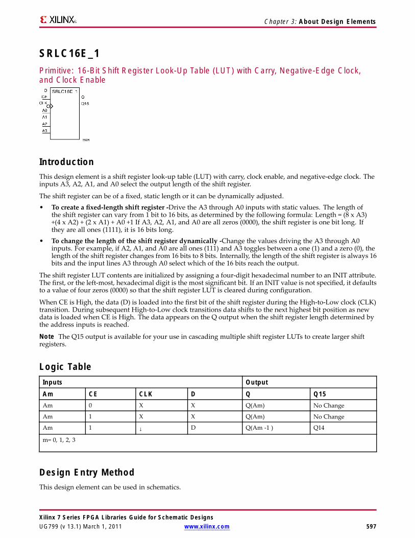
Chapter 3: About Design Elements
SRLC16E_1Primitive: 16-Bit Shift Register Look-Up Table (LUT) with Carry, Negative-Edge Clock,and Clock Enable
IntroductionThis design element is a shift register look-up table (LUT) with carry, clock enable, and negative-edge clock. Theinputs A3, A2, A1, and A0 select the output length of the shift register.
The shift register can be of a fixed, static length or it can be dynamically adjusted.• To create a fixed-length shift register -Drive the A3 through A0 inputs with static values. The length of
the shift register can vary from 1 bit to 16 bits, as determined by the following formula: Length = (8 x A3)+(4 x A2) + (2 x A1) + A0 +1 If A3, A2, A1, and A0 are all zeros (0000), the shift register is one bit long. Ifthey are all ones (1111), it is 16 bits long.
• To change the length of the shift register dynamically -Change the values driving the A3 through A0inputs. For example, if A2, A1, and A0 are all ones (111) and A3 toggles between a one (1) and a zero (0), thelength of the shift register changes from 16 bits to 8 bits. Internally, the length of the shift register is always 16bits and the input lines A3 through A0 select which of the 16 bits reach the output.
The shift register LUT contents are initialized by assigning a four-digit hexadecimal number to an INIT attribute.The first, or the left-most, hexadecimal digit is the most significant bit. If an INIT value is not specified, it defaultsto a value of four zeros (0000) so that the shift register LUT is cleared during configuration.
When CE is High, the data (D) is loaded into the first bit of the shift register during the High-to-Low clock (CLK)transition. During subsequent High-to-Low clock transitions data shifts to the next highest bit position as newdata is loaded when CE is High. The data appears on the Q output when the shift register length determined bythe address inputs is reached.
Note The Q15 output is available for your use in cascading multiple shift register LUTs to create larger shiftregisters.
Logic TableInputs Output
Am CE CLK D Q Q15Am 0 X X Q(Am) No Change
Am 1 X X Q(Am) No Change
Am 1 ↓ D Q(Am -1 ) Q14
m= 0, 1, 2, 3
Design Entry MethodThis design element can be used in schematics.
Xilinx 7 Series FPGA Libraries Guide for Schematic DesignsUG799 (v 13.1) March 1, 2011 www.xilinx.com 597

Chapter 3: About Design Elements
Available Attributes
Attribute TypeAllowedValues Default Description
INIT Hexadecimal Any 16-BitValue
All zeros Sets the initial value of content and output of shift registerafter configuration.
For More InformationSee the 7 series FPGA User Documentation (User Guides and Data Sheets).
Xilinx 7 Series FPGA Libraries Guide for Schematic Designs598 www.xilinx.com UG799 (v 13.1) March 1, 2011

Chapter 3: About Design Elements
SRLC32EPrimitive: 32 Clock Cycle, Variable Length Shift Register Look-Up Table (LUT) with ClockEnable
IntroductionThis design element is a variable length, 1 to 32 clock cycle shift register implemented within a single look-uptable (LUT). The shift register can be of a fixed length, static length, or it can be dynamically adjusted by changingthe address lines to the component. This element also features an active, high-clock enable and a cascadingfeature in which multiple SRLC32Es can be cascaded in order to create greater shift lengths.
Port DescriptionsPort Direction Width FunctionQ Output 1 Shift register data output
Q31 Output 1 Shift register cascaded output (connect to the D inputof a subsequent SRLC32E)
D Input 1 Shift register data input
CLK Input 1 Clock
CE Input 1 Active high clock enable
A Input 5 Dynamic depth selection of the SRL
A=00000 ==> 1-bit shift length
A=11111 ==> 32-bit shift length
Design Entry MethodThis design element can be used in schematics.
If instantiated, the following connections should be made to this component:• Connect the CLK input to the desired clock source, the D input to the data source to be shifted/stored and the
Q output to either an FDCPE or an FDRSE input or other appropriate data destination.• The CE clock enable pin can be connected to a clock enable signal in the design or else tied to a logic one
if not used.• The 5-bit A bus can either be tied to a static value between 0 and 31 to signify a fixed 1 to 32 bit static shift
length, or else it can be tied to the appropriate logic to enable a varying shift depth anywhere between 1and 32 bits.
• If you want to create a longer shift length than 32, connect the Q31 output pin to the D input pin of asubsequent SRLC32E to cascade and create larger shift registers.
• It is not valid to connect the Q31 output to anything other than another SRLC32E.• The selectable Q output is still available in the cascaded mode, if needed.• An optional INIT attribute consisting of a 32-bit Hexadecimal value can be specified to indicate the initial
shift pattern of the shift register.• (INIT[0] will be the first value shifted out.)
Xilinx 7 Series FPGA Libraries Guide for Schematic DesignsUG799 (v 13.1) March 1, 2011 www.xilinx.com 599
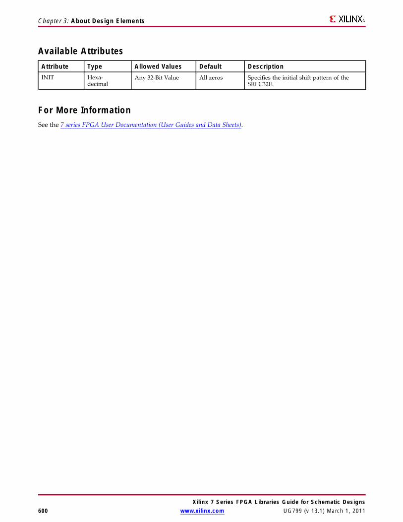
Chapter 3: About Design Elements
Available AttributesAttribute Type Allowed Values Default DescriptionINIT Hexa-
decimalAny 32-Bit Value All zeros Specifies the initial shift pattern of the
SRLC32E.
For More InformationSee the 7 series FPGA User Documentation (User Guides and Data Sheets).
Xilinx 7 Series FPGA Libraries Guide for Schematic Designs600 www.xilinx.com UG799 (v 13.1) March 1, 2011

Chapter 3: About Design Elements
STARTUPE2Primitive: STARTUP Block
IntroductionThis design element is used to interface device pins and logic to the global asynchronous set/reset (GSR)signal, the global 3-state (GTS) dedicated routing, the internal configuration signals, or a few of the dedicatedconfiguration pins.
Port DescriptionsPort Type Width FunctionCFGCLK Output 1 Configuration main clock output
CFGMCLK Output 1 Configuration internal oscillator clock output
CLK Input 1 User startup clock input
EOS Output 1 Active high output signal indicating the end of startup.
GSR Input 1 Global Set/Reset input (GSR cannot be used for the port name)
GTS Input 1 Global 3-state input (GTS cannot be used for the port name)
KEYCLEARB Input 1 Clear AES Decrypter Key input from Battery-Backed RAM (BBRAM)
PACK Input 1 PROGRAM acknowledge input
PREQ Output 1 PROGRAM request to fabric output
USRCCLKO Input 1 User CCLK input
USRCCLKTS Input 1 User CCLK 3-state enable input
USRDONEO Input 1 User DONE pin output control
USRDONETS Input 1 User DONE 3-state enable output
Design Entry MethodThis design element can be used in schematics.
Xilinx 7 Series FPGA Libraries Guide for Schematic DesignsUG799 (v 13.1) March 1, 2011 www.xilinx.com 601

Chapter 3: About Design Elements
Available AttributesAttribute Type Allowed Values Default DescriptionPROG_USR STRING FALSE, TRUE FALSE Activate program event security
feature.
SIM_CCLK_FREQ FLOAT(nS) 0.0 to any value 0.0 Set the Configuration ClockFrequency(ns) for simulation.
For More InformationSee the 7 series FPGA User Documentation (User Guides and Data Sheets).
Xilinx 7 Series FPGA Libraries Guide for Schematic Designs602 www.xilinx.com UG799 (v 13.1) March 1, 2011

Chapter 3: About Design Elements
USR_ACCESSE2Primitive: Configuration Data Access
IntroductionThis design element enables you to access a 32-bit register within the configuration logic. This enables thefabric to access data that can be set from the bitstream.
Port DescriptionsPort Type Width FunctionCFGCLK Output 1 Configuration Clock output
DATA<31:0> Output 32 Configuration Data output
DATAVALID Output 1 Active high data valid output
Design Entry MethodThis design element can be used in schematics.
For More Information• See the 7 series FPGA SelectIO Resources User Guide.
• See the 7 series FPGA Data Sheet DC and Switching Characteristics.
Xilinx 7 Series FPGA Libraries Guide for Schematic DesignsUG799 (v 13.1) March 1, 2011 www.xilinx.com 603

Chapter 3: About Design Elements
VCCPrimitive: VCC-Connection Signal Tag
IntroductionThis design element serves as a signal tag, or parameter, that forces a net or input function to a logic High level.A net tied to this element cannot have any other source.
When the placement and routing software encounters a net or input function tied to this element, it removes anylogic that is disabled by the Vcc signal, which is only implemented when the disabled logic cannot be removed.
Design Entry MethodThis design element is only for use in schematics.
For More InformationSee the 7 series FPGA User Documentation (User Guides and Data Sheets).
Xilinx 7 Series FPGA Libraries Guide for Schematic Designs604 www.xilinx.com UG799 (v 13.1) March 1, 2011

Chapter 3: About Design Elements
XADCPrimitive: Xilinx Analog-to-Digital Converter
IntroductionLarger members of the 7 series FPGA family contains a single XADC block. The XADC function is built arounda 12-bit, 1Msps (megasamples per second) dual Analog-to-Digital Converter (ADC). When combined with anumber of on-chip sensors, the XADC is used to measure FPGA physical operating parameters like on-chippower supply voltages and die temperatures. Access to external voltages is provided through a dedicatedanalog-input pair (VP/VN) and up to 16 user-selectable analog inputs, known as auxiliary analog inputs(VAUXP[15:0], VAUXN[15:0]). The external analog inputs allow the XADC to monitor the physical environmentof the board or enclosure. XADC is fully functional on power up, and measurement data can be accessed viathe JTAG port pre-configuration. The XADC control logic implements some common monitoring features. Forexample, an automatic channel sequencer allows a user-defined selection of parameters to be automaticallymonitored, and user-programmable averaging is enabled to ensure robust noise-free measurements. XADC alsoprovides user-programmable alarm thresholds for the on-chip sensors. Thus, if an on-chip monitored parametermoves outside the user-specified operating range, an alarm logic output becomes active.
Xilinx 7 Series FPGA Libraries Guide for Schematic DesignsUG799 (v 13.1) March 1, 2011 www.xilinx.com 605
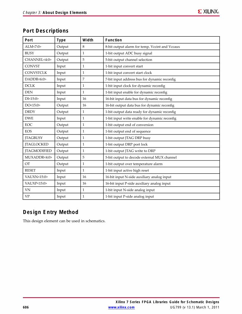
Chapter 3: About Design Elements
Port DescriptionsPort Type Width FunctionALM<7:0> Output 8 8-bit output alarm for temp, Vccint and Vccaux
BUSY Output 1 1-bit output ADC busy signal
CHANNEL<4:0> Output 5 5-bit output channel selection
CONVST Input 1 1-bit input convert start
CONVSTCLK Input 1 1-bit input convert start clock
DADDR<6:0> Input 7 7-bit input address bus for dynamic reconfig
DCLK Input 1 1-bit input clock for dynamic reconfig
DEN Input 1 1-bit input enable for dynamic reconfig
DI<15:0> Input 16 16-bit input data bus for dynamic reconfig
DO<15:0> Output 16 16-bit output data bus for dynamic reconfig
DRDY Output 1 1-bit output data ready for dynamic reconfig
DWE Input 1 1-bit input write enable for dynamic reconfig
EOC Output 1 1-bit output end of conversion
EOS Output 1 1-bit output end of sequence
JTAGBUSY Output 1 1-bit output JTAG DRP busy
JTAGLOCKED Output 1 1-bit output DRP port lock
JTAGMODIFIED Output 1 1-bit output JTAG write to DRP
MUXADDR<4:0> Output 5 5-bit output to decode external MUX channel
OT Output 1 1-bit output over temperature alarm
RESET Input 1 1-bit input active high reset
VAUXN<15:0> Input 16 16-bit input N-side auxiliary analog input
VAUXP<15:0> Input 16 16-bit input P-side auxiliary analog input
VN Input 1 1-bit input N-side analog input
VP Input 1 1-bit input P-side analog input
Design Entry MethodThis design element can be used in schematics.
Xilinx 7 Series FPGA Libraries Guide for Schematic Designs606 www.xilinx.com UG799 (v 13.1) March 1, 2011

Chapter 3: About Design Elements
Available AttributesAttribute Type Allowed Values Default DescriptionINIT_4A HEX 16’h0000 to 16’hffff 16’h0000 Sequence register 2
INIT_4B HEX 16’h0000 to 16’hffff 16’h0000 Sequence register 3
INIT_4C HEX 16’h0000 to 16’hffff 16’h0000 Sequence register 4
INIT_4D HEX 16’h0000 to 16’hffff 16’h0000 Sequence register 5
INIT_4E HEX 16’h0000 to 16’hffff 16’h0000 Sequence register 6
INIT_4F HEX 16’h0000 to 16’hffff 16’h0000 Sequence register 7
INIT_5A HEX 16’h0000 to 16’hffff 16’h0000 Reserved for future use
INIT_5B HEX 16’h0000 to 16’hffff 16’h0000 Reserved for future use
INIT_5C HEX 16’h0000 to 16’hffff 16’h0000 CCram lower alarm threshold
INIT_5D HEX 16’h0000 to 16’hffff 16’h0000 Reserved for future use
INIT_5E HEX 16’h0000 to 16’hffff 16’h0000 Reserved for future use
INIT_5F HEX 16’h0000 to 16’hffff 16’h0000 Reserved for future use
INIT_40 HEX 16’h0000 to 16’hffff 16’h0000 Configuration register 0
INIT_41 HEX 16’h0000 to 16’hffff 16’h0000 Configuration register 1
INIT_42 HEX 16’h0000 to 16’hffff 16’h0800 Configuration register 2
INIT_43 HEX 16’h0000 to 16’hffff 16’h0000 Test register 0
INIT_44 HEX 16’h0000 to 16’hffff 16’h0000 Test register 1
INIT_45 HEX 16’h0000 to 16’hffff 16’h0000 Test register 2
INIT_46 HEX 16’h0000 to 16’hffff 16’h0000 Test register 3
INIT_47 HEX 16’h0000 to 16’hffff 16’h0000 Test register 4
INIT_48 HEX 16’h0000 to 16’hffff 16’h0000 Sequence register 0
INIT_49 HEX 16’h0000 to 16’hffff 16’h0000 Sequence register 1
INIT_50 HEX 16’h0000 to 16’hffff 16’h0000 Alarm limit register 0
INIT_51 HEX 16’h0000 to 16’hffff 16’h0000 Alarm limit register 1
INIT_52 HEX 16’h0000 to 16’hffff 16’h0000 Alarm limit register 2
INIT_53 HEX 16’h0000 to 16’hffff 16’h0000 Alarm limit register 3
INIT_54 HEX 16’h0000 to 16’hffff 16’h0000 Alarm limit register 4
INIT_55 HEX 16’h0000 to 16’hffff 16’h0000 Alarm limit register 5
INIT_56 HEX 16’h0000 to 16’hffff 16’h0000 Alarm limit register 6
INIT_57 HEX 16’h0000 to 16’hffff 16’h0000 Alarm limit register 7
INIT_58 HEX 16’h0000 to 16’hffff 16’h0000 CCram upper alarm threshold
INIT_59 HEX 16’h0000 to 16’hffff 16’h0000 Reserved for future use
SIM_MONITOR_FILE
STRING 0 bit STRING design.txt Simulation analog entry file
For More InformationSee the 7 series FPGA User Documentation (User Guides and Data Sheets).
Xilinx 7 Series FPGA Libraries Guide for Schematic DesignsUG799 (v 13.1) March 1, 2011 www.xilinx.com 607

Chapter 3: About Design Elements
XNOR2Primitive: 2-Input XNOR Gate with Non-Inverted Inputs
IntroductionXNOR functions of up to nine inputs are available. All inputs are non-inverting. Because each input uses a CLBresource, replace functions with unused inputs with functions having the necessary number of inputs.
Logic TableInput OutputI0 ... Iz O
Odd number of 1 0
Even number of 1 1
Design Entry MethodThis design element is only for use in schematics.
For More InformationSee the 7 series FPGA User Documentation (User Guides and Data Sheets).
Xilinx 7 Series FPGA Libraries Guide for Schematic Designs608 www.xilinx.com UG799 (v 13.1) March 1, 2011
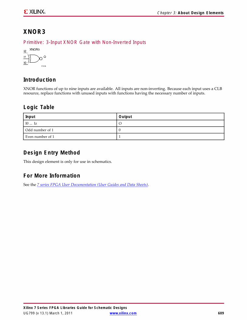
Chapter 3: About Design Elements
XNOR3Primitive: 3-Input XNOR Gate with Non-Inverted Inputs
IntroductionXNOR functions of up to nine inputs are available. All inputs are non-inverting. Because each input uses a CLBresource, replace functions with unused inputs with functions having the necessary number of inputs.
Logic TableInput OutputI0 ... Iz O
Odd number of 1 0
Even number of 1 1
Design Entry MethodThis design element is only for use in schematics.
For More InformationSee the 7 series FPGA User Documentation (User Guides and Data Sheets).
Xilinx 7 Series FPGA Libraries Guide for Schematic DesignsUG799 (v 13.1) March 1, 2011 www.xilinx.com 609

Chapter 3: About Design Elements
XNOR4Primitive: 4-Input XNOR Gate with Non-Inverted Inputs
IntroductionXNOR functions of up to nine inputs are available. All inputs are non-inverting. Because each input uses a CLBresource, replace functions with unused inputs with functions having the necessary number of inputs.
Logic TableInput OutputI0 ... Iz O
Odd number of 1 0
Even number of 1 1
Design Entry MethodThis design element is only for use in schematics.
For More InformationSee the 7 series FPGA User Documentation (User Guides and Data Sheets).
Xilinx 7 Series FPGA Libraries Guide for Schematic Designs610 www.xilinx.com UG799 (v 13.1) March 1, 2011

Chapter 3: About Design Elements
XNOR5Primitive: 5-Input XNOR Gate with Non-Inverted Inputs
IntroductionXNOR functions of up to nine inputs are available. All inputs are non-inverting. Because each input uses a CLBresource, replace functions with unused inputs with functions having the necessary number of inputs.
Logic TableInput OutputI0 ... Iz O
Odd number of 1 0
Even number of 1 1
Design Entry MethodThis design element is only for use in schematics.
For More InformationSee the 7 series FPGA User Documentation (User Guides and Data Sheets).
Xilinx 7 Series FPGA Libraries Guide for Schematic DesignsUG799 (v 13.1) March 1, 2011 www.xilinx.com 611

Chapter 3: About Design Elements
XNOR6Macro: 6-Input XNOR Gate with Non-Inverted Inputs
IntroductionXNOR functions of up to nine inputs are available. All inputs are non-inverting. Because each input uses a CLBresource, replace functions with unused inputs with functions having the necessary number of inputs.
Logic TableInput OutputI0 ... Iz O
Odd number of 1 0
Even number of 1 1
Design Entry MethodThis design element is only for use in schematics.
For More InformationSee the 7 series FPGA User Documentation (User Guides and Data Sheets).
Xilinx 7 Series FPGA Libraries Guide for Schematic Designs612 www.xilinx.com UG799 (v 13.1) March 1, 2011

Chapter 3: About Design Elements
XNOR7Macro: 7-Input XNOR Gate with Non-Inverted Inputs
IntroductionXNOR functions of up to nine inputs are available. All inputs are non-inverting. Because each input uses a CLBresource, replace functions with unused inputs with functions having the necessary number of inputs.
Logic TableInput OutputI0 ... Iz O
Odd number of 1 0
Even number of 1 1
Design Entry MethodThis design element is only for use in schematics.
For More InformationSee the 7 series FPGA User Documentation (User Guides and Data Sheets).
Xilinx 7 Series FPGA Libraries Guide for Schematic DesignsUG799 (v 13.1) March 1, 2011 www.xilinx.com 613

Chapter 3: About Design Elements
XNOR8Macro: 8-Input XNOR Gate with Non-Inverted Inputs
IntroductionXNOR functions of up to nine inputs are available. All inputs are non-inverting. Because each input uses a CLBresource, replace functions with unused inputs with functions having the necessary number of inputs.
Logic TableInput OutputI0 ... Iz O
Odd number of 1 0
Even number of 1 1
Design Entry MethodThis design element is only for use in schematics.
For More InformationSee the 7 series FPGA User Documentation (User Guides and Data Sheets).
Xilinx 7 Series FPGA Libraries Guide for Schematic Designs614 www.xilinx.com UG799 (v 13.1) March 1, 2011

Chapter 3: About Design Elements
XNOR9Macro: 9-Input XNOR Gate with Non-Inverted Inputs
IntroductionXNOR functions of up to nine inputs are available. All inputs are non-inverting. Because each input uses a CLBresource, replace functions with unused inputs with functions having the necessary number of inputs.
Logic TableInput OutputI0 ... Iz O
Odd number of 1 0
Even number of 1 1
Design Entry MethodThis design element is only for use in schematics.
For More InformationSee the 7 series FPGA User Documentation (User Guides and Data Sheets).
Xilinx 7 Series FPGA Libraries Guide for Schematic DesignsUG799 (v 13.1) March 1, 2011 www.xilinx.com 615

Chapter 3: About Design Elements
XOR2Primitive: 2-Input XOR Gate with Non-Inverted Inputs
IntroductionXOR functions of up to nine inputs are available. All inputs are non-inverting. Because each input uses a CLBresource, replace functions with unused inputs with functions having the necessary number of inputs.
Design Entry MethodThis design element is only for use in schematics.
For More InformationSee the 7 series FPGA User Documentation (User Guides and Data Sheets).
Xilinx 7 Series FPGA Libraries Guide for Schematic Designs616 www.xilinx.com UG799 (v 13.1) March 1, 2011

Chapter 3: About Design Elements
XOR3Primitive: 3-Input XOR Gate with Non-Inverted Inputs
IntroductionXOR functions of up to nine inputs are available. All inputs are non-inverting. Because each input uses a CLBresource, replace functions with unused inputs with functions having the necessary number of inputs.
Design Entry MethodThis design element is only for use in schematics.
For More InformationSee the 7 series FPGA User Documentation (User Guides and Data Sheets).
Xilinx 7 Series FPGA Libraries Guide for Schematic DesignsUG799 (v 13.1) March 1, 2011 www.xilinx.com 617

Chapter 3: About Design Elements
XOR4Primitive: 4-Input XOR Gate with Non-Inverted Inputs
IntroductionXOR functions of up to nine inputs are available. All inputs are non-inverting. Because each input uses a CLBresource, replace functions with unused inputs with functions having the necessary number of inputs.
Design Entry MethodThis design element is only for use in schematics.
For More InformationSee the 7 series FPGA User Documentation (User Guides and Data Sheets).
Xilinx 7 Series FPGA Libraries Guide for Schematic Designs618 www.xilinx.com UG799 (v 13.1) March 1, 2011

Chapter 3: About Design Elements
XOR5Primitive: 5-Input XOR Gate with Non-Inverted Inputs
IntroductionXOR functions of up to nine inputs are available. All inputs are non-inverting. Because each input uses a CLBresource, replace functions with unused inputs with functions having the necessary number of inputs.
Design Entry MethodThis design element is only for use in schematics.
For More InformationSee the 7 series FPGA User Documentation (User Guides and Data Sheets).
Xilinx 7 Series FPGA Libraries Guide for Schematic DesignsUG799 (v 13.1) March 1, 2011 www.xilinx.com 619

Chapter 3: About Design Elements
XOR6Macro: 6-Input XOR Gate with Non-Inverted Inputs
IntroductionXOR functions of up to nine inputs are available. All inputs are non-inverting. Because each input uses a CLBresource, replace functions with unused inputs with functions having the necessary number of inputs.
Design Entry MethodThis design element is only for use in schematics.
For More InformationSee the 7 series FPGA User Documentation (User Guides and Data Sheets).
Xilinx 7 Series FPGA Libraries Guide for Schematic Designs620 www.xilinx.com UG799 (v 13.1) March 1, 2011

Chapter 3: About Design Elements
XOR7Macro: 7-Input XOR Gate with Non-Inverted Inputs
IntroductionXOR functions of up to nine inputs are available. All inputs are non-inverting. Because each input uses a CLBresource, replace functions with unused inputs with functions having the necessary number of inputs.
Design Entry MethodThis design element is only for use in schematics.
For More InformationSee the 7 series FPGA User Documentation (User Guides and Data Sheets).
Xilinx 7 Series FPGA Libraries Guide for Schematic DesignsUG799 (v 13.1) March 1, 2011 www.xilinx.com 621

Chapter 3: About Design Elements
XOR8Macro: 8-Input XOR Gate with Non-Inverted Inputs
IntroductionXOR functions of up to nine inputs are available. All inputs are non-inverting. Because each input uses a CLBresource, replace functions with unused inputs with functions having the necessary number of inputs.
Design Entry MethodThis design element is only for use in schematics.
For More InformationSee the 7 series FPGA User Documentation (User Guides and Data Sheets).
Xilinx 7 Series FPGA Libraries Guide for Schematic Designs622 www.xilinx.com UG799 (v 13.1) March 1, 2011
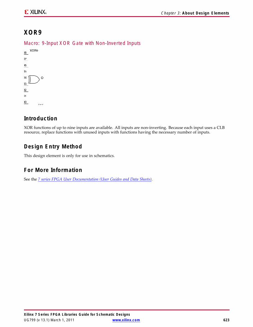
Chapter 3: About Design Elements
XOR9Macro: 9-Input XOR Gate with Non-Inverted Inputs
IntroductionXOR functions of up to nine inputs are available. All inputs are non-inverting. Because each input uses a CLBresource, replace functions with unused inputs with functions having the necessary number of inputs.
Design Entry MethodThis design element is only for use in schematics.
For More InformationSee the 7 series FPGA User Documentation (User Guides and Data Sheets).
Xilinx 7 Series FPGA Libraries Guide for Schematic DesignsUG799 (v 13.1) March 1, 2011 www.xilinx.com 623
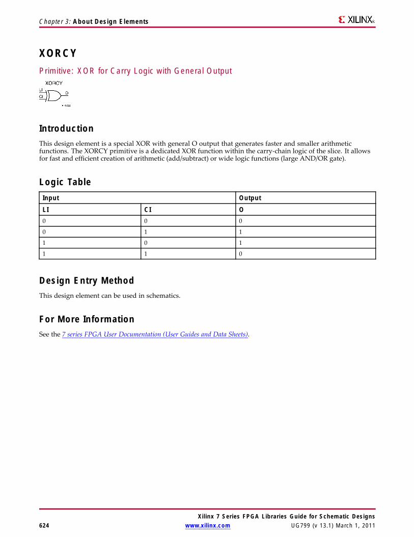
Chapter 3: About Design Elements
XORCYPrimitive: XOR for Carry Logic with General Output
IntroductionThis design element is a special XOR with general O output that generates faster and smaller arithmeticfunctions. The XORCY primitive is a dedicated XOR function within the carry-chain logic of the slice. It allowsfor fast and efficient creation of arithmetic (add/subtract) or wide logic functions (large AND/OR gate).
Logic TableInput Output
LI CI O0 0 0
0 1 1
1 0 1
1 1 0
Design Entry MethodThis design element can be used in schematics.
For More InformationSee the 7 series FPGA User Documentation (User Guides and Data Sheets).
Xilinx 7 Series FPGA Libraries Guide for Schematic Designs624 www.xilinx.com UG799 (v 13.1) March 1, 2011