xilinx schematic entry tutorial r2 - university of southern · pdf file ·...
TRANSCRIPT

9/1/2008 Xilinx™ Schematic Entry Tutorial 1
Xilinx™ Schematic Entry Tutorial
Xilinx™ ISE Schematic Entry &
Modelsim Simulation
ByBilal Zafar and Gandhi Puvvada
Rev: 2.0September 1, 2008

9/1/2008 Xilinx™ Schematic Entry Tutorial 2
Overview
What is circuit simulation and why is it important?• Complex designs, short design cycle• Simultaneous system design and hardware design
Design Entry Options• Schematics• HDL
Types of Simulation• Behavioral Simulation• Timing Simulation (post place & route)
Tool or Design Flow that we will use• Create schematics using Xilinx Schematic Editor• Run simulations using a Verilog Test Fixture in Modelsim Simulator
Implement and download to Nexys2• TOP design to connect to I/O resources on Nexys2 board• Adept tool to download
9/1/2008 Xilinx™ Schematic Entry Tutorial 3
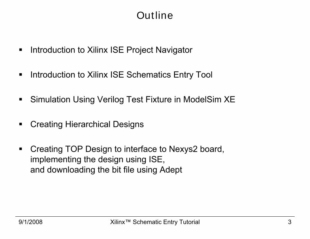
Outline
Introduction to Xilinx ISE Project Navigator
Introduction to Xilinx ISE Schematics Entry Tool
Simulation Using Verilog Test Fixture in ModelSim XE
Creating Hierarchical Designs
Creating TOP Design to interface to Nexys2 board,implementing the design using ISE, and downloading the bit file using Adept

9/1/2008 Xilinx™ Schematic Entry Tutorial 4
Introduction to Xilinx ISE Project Navigator
Project Navigator: an integrated environment • create a project with many design files, etc.• enter our design (schematics and Verilog)• write test bench for the design• launch ModelSim XE simulator to run simulations• synthesize the design for FPGA board• program the FPGA • debug the FPGA-based design using ChipScope
9/1/2008 Xilinx™ Schematic Entry Tutorial 5
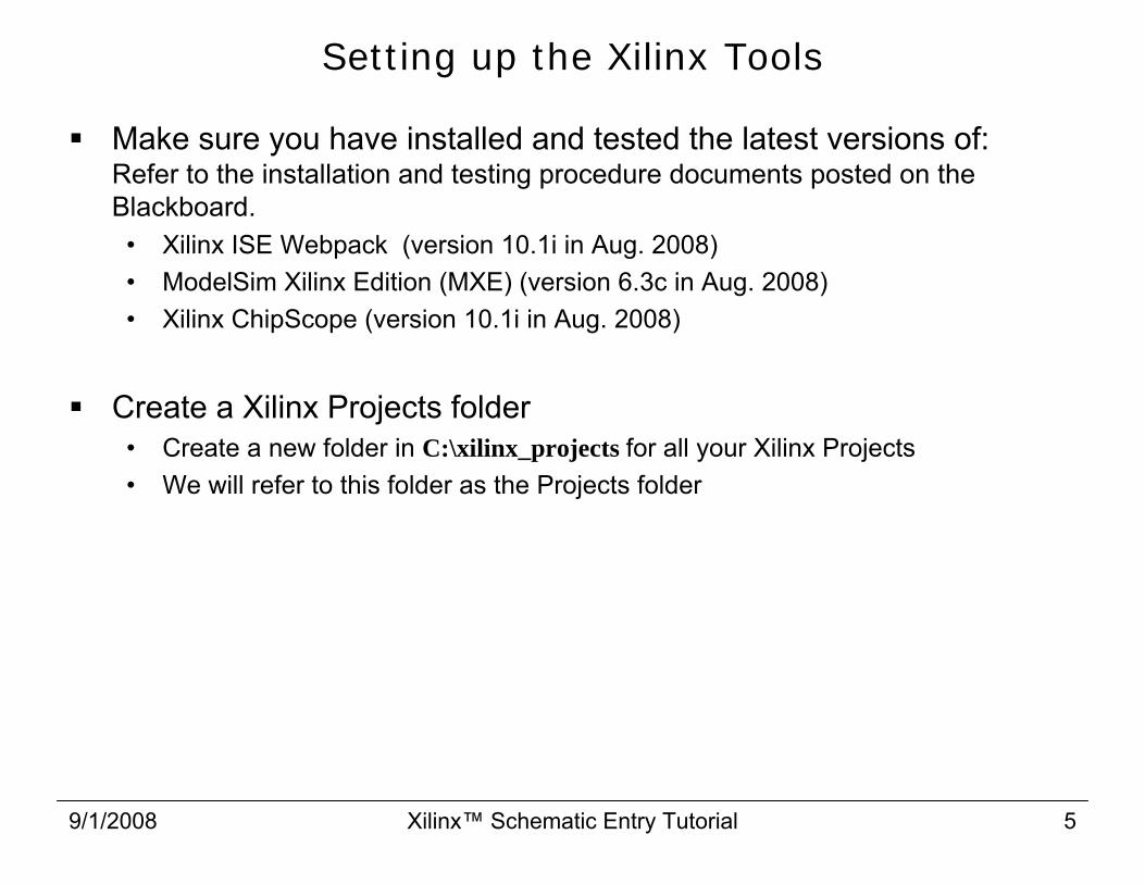
Setting up the Xilinx Tools
Make sure you have installed and tested the latest versions of:Refer to the installation and testing procedure documents posted on the Blackboard.• Xilinx ISE Webpack (version 10.1i in Aug. 2008)• ModelSim Xilinx Edition (MXE) (version 6.3c in Aug. 2008)• Xilinx ChipScope (version 10.1i in Aug. 2008)
Create a Xilinx Projects folder• Create a new folder in C:\xilinx_projects for all your Xilinx Projects• We will refer to this folder as the Projects folder
9/1/2008 Xilinx™ Schematic Entry Tutorial 6
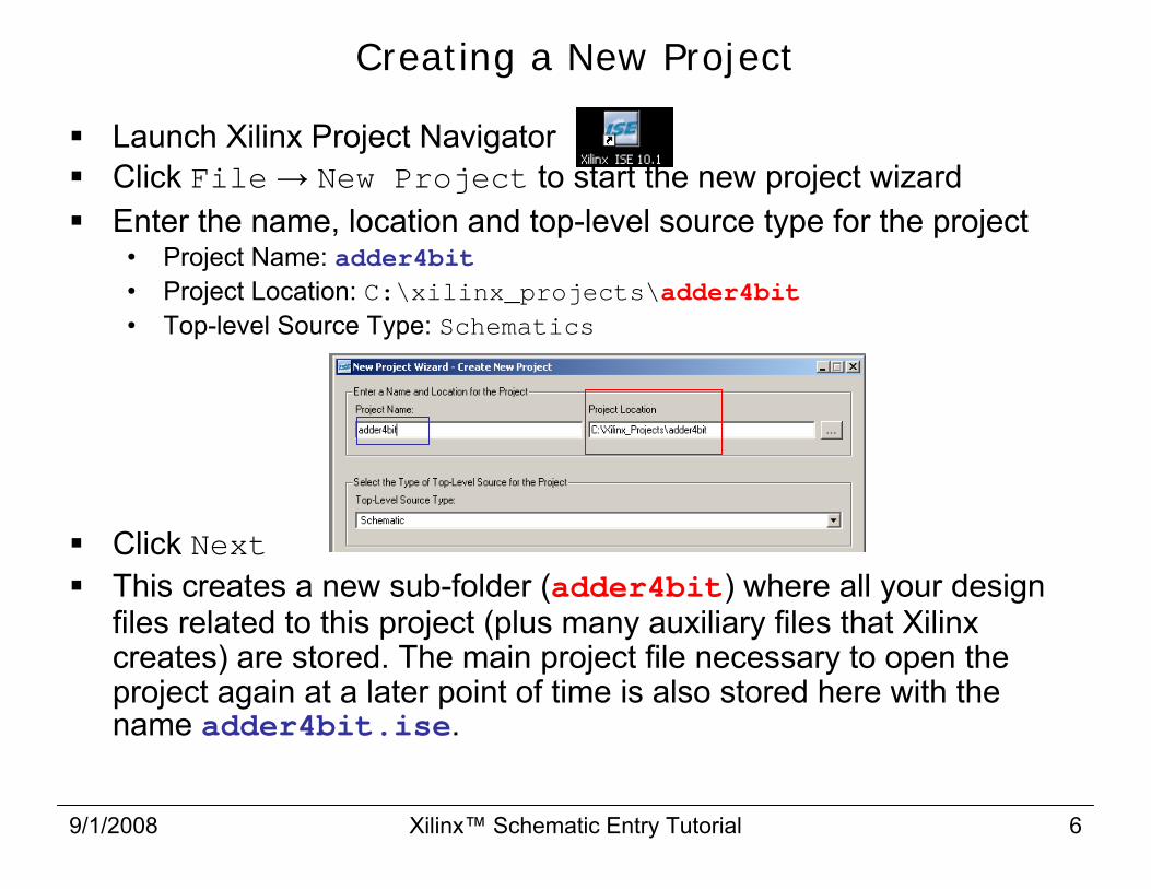
Creating a New Project
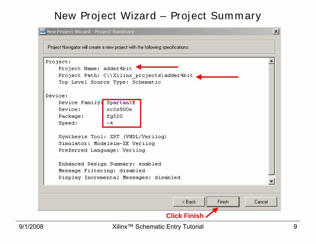
Launch Xilinx Project NavigatorClick File→ New Project to start the new project wizard Enter the name, location and top-level source type for the project • Project Name: adder4bit• Project Location: C:\xilinx_projects\adder4bit• Top-level Source Type: Schematics
Click NextThis creates a new sub-folder (adder4bit) where all your design files related to this project (plus many auxiliary files that Xilinx creates) are stored. The main project file necessary to open theproject again at a later point of time is also stored here with the name adder4bit.ise.
9/1/2008 Xilinx™ Schematic Entry Tutorial 7
Expand the pull-down choices to get to know
FPGA on the Nexys2 board
Schematic/HDL
9/1/2008 Xilinx™ Schematic Entry Tutorial 8
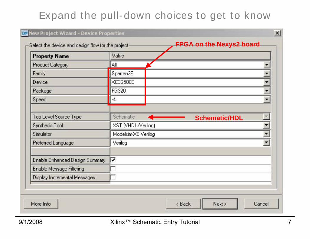
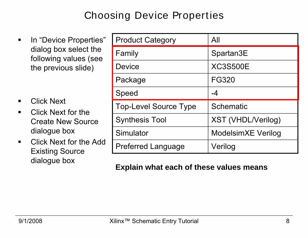
Choosing Device Properties
In “Device Properties” dialog box select the following values (see the previous slide)
Click NextClick Next for the Create New Source dialogue boxClick Next for the Add Existing Source dialogue box
VerilogPreferred Language
ModelsimXE VerilogSimulator
XST (VHDL/Verilog)Synthesis Tool
SchematicTop-Level Source Type
-4Speed
FG320Package
XC3S500EDevice
Spartan3EFamily
AllProduct Category
Explain what each of these values means
9/1/2008 Xilinx™ Schematic Entry Tutorial 9
New Project Wizard – Project Summary
Click Finish
9/1/2008 Xilinx™ Schematic Entry Tutorial 10
Getting to Know the Project Navigator
1. Toolbar• Basic file management tools• Process specific tools for the selected process
2. Sources Window• Shows the design hierarchy with all source files• Different views available (see 3)
3. Sources View (in the Sources Window)
4. Processes Window• Show available processes for the selected source
5. Transcript window: • Space where warnings and error messages are
reported
6. Workspace: the playing field!
1
2
4
5
6
3
9/1/2008 Xilinx™ Schematic Entry Tutorial 11
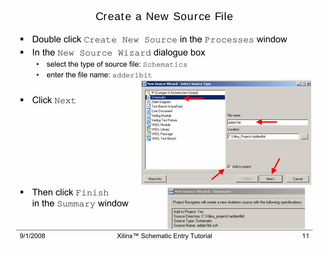
Create a New Source File
Double click Create New Source in the Processes windowIn the New Source Wizard dialogue box• select the type of source file: Schematics• enter the file name: adder1bit
Click Next
Then click Finishin the Summary window
9/1/2008 Xilinx™ Schematic Entry Tutorial 12
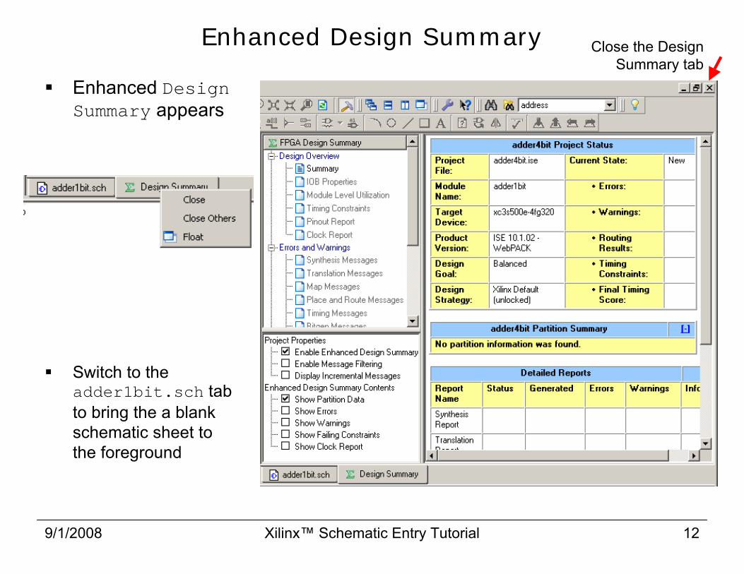
Enhanced Design Summary
Enhanced Design Summary appears
Switch to the adder1bit.sch tab to bring the a blank schematic sheet to the foreground
Close the Design Summary tab

9/1/2008 Xilinx™ Schematic Entry Tutorial 13
Getting to Know the Xilinx Schematic Editor
1. Toolbar• new buttons for schematic entry
2. Symbols Tab• Categories• Symbols• Symbol Name Filter• Orientation• Symbol Info (links to Xilinx Libraries
Guide to show component’s data sheet)
3. Options TabShows options related to the selected task
4. Schematic Editor Workspace
You can detach the Schematic from the Project Navigator by right-clicking at the schematic file name tab (adder1bit.sch) and selecting Float
1
2
3
4
Size
9/1/2008 Xilinx™ Schematic Entry Tutorial 14
Outline
Introduction to Xilinx ISE Project Navigator
Introduction to Xilinx ISE Schematics Entry Tool
Simulation Using Verilog Test Fixture in ModelSim XE
Creating Hierarchical Designs
Creating TOP Design to interface to Nexys2 board,implementing the design using ISE, and downloading the bit file using Adept
9/1/2008 Xilinx™ Schematic Entry Tutorial 15
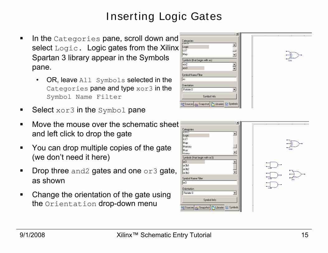
Inserting Logic Gates
In the Categories pane, scroll down and select Logic. Logic gates from the Xilinx Spartan 3 library appear in the Symbols pane.
• OR, leave All Symbols selected in the Categories pane and type xor3 in the Symbol Name Filter
Select xor3 in the Symbol pane
Move the mouse over the schematic sheet and left click to drop the gate
You can drop multiple copies of the gate (we don’t need it here)
Drop three and2 gates and one or3 gate, as shown
Change the orientation of the gate using the Orientation drop-down menu

9/1/2008 Xilinx™ Schematic Entry Tutorial 16
Schematic Editing Toolbar
Zoom controlsPop to the next higher level
Rename Selected Bus
Add SymbolAdd Instance Name
Zoom back and forth
Push into a symbolAdd drawing & textCheck Schematic
Add Input/Output markerAdd bus tap
Add Net NameAdd wire Select tool (default)

9/1/2008 Xilinx™ Schematic Entry Tutorial 17
Adding Wires and Buses
To add a net (wire or bus)• Click on the Add wire toolbar button • Or, press Ctrl+w
To connect a net to a pin, bring the mouse pointer close to the pinThe four square boxes next to the pin indicate that the added net will snap to this pinUse “press-drag-release” to draw a netTo create branching, place the pointer’s centre on the net and press-drag-releaseWhen connecting two nets, a solid blue dot at the intersection indicates that nets are connected• = connected; = not connected
Add Wire Options appear under the Options tab

9/1/2008 Xilinx™ Schematic Entry Tutorial 18
Complete Wiring of adder1bit
Complete the wiring as shown here
9/1/2008 Xilinx™ Schematic Entry Tutorial 19
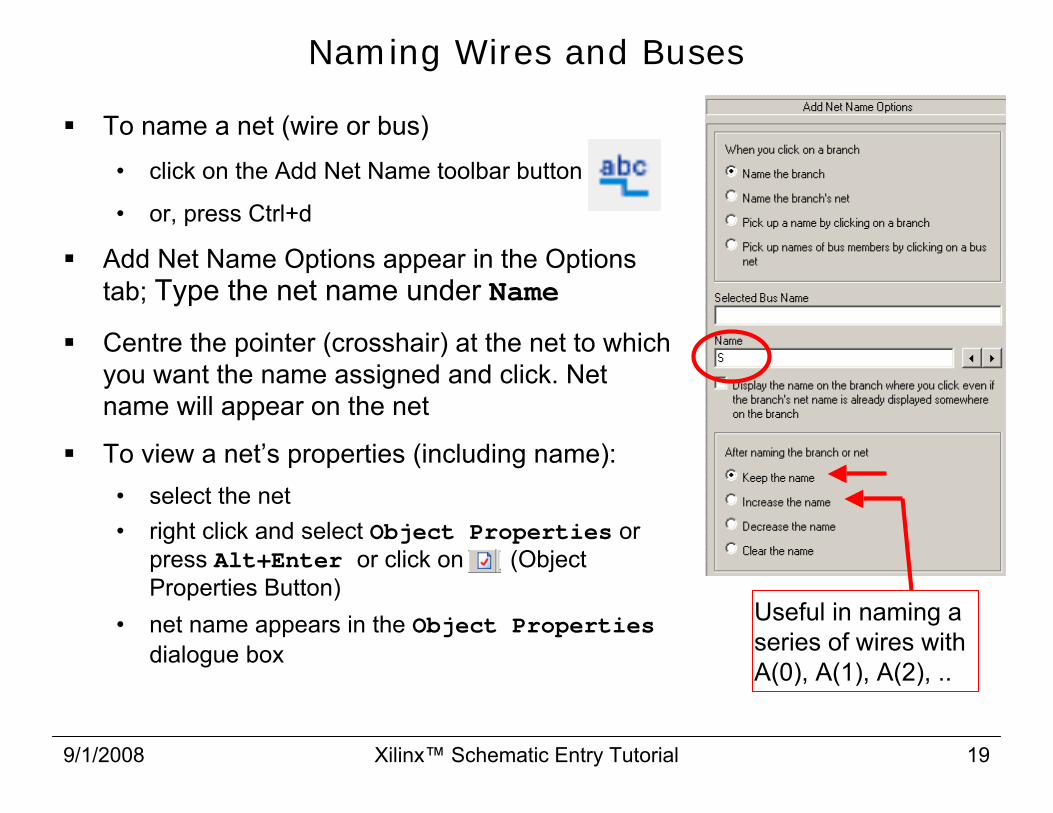
Naming Wires and Buses
To name a net (wire or bus)
• click on the Add Net Name toolbar button
• or, press Ctrl+d
Add Net Name Options appear in the Options tab; Type the net name under Name
Centre the pointer (crosshair) at the net to which you want the name assigned and click. Net name will appear on the net
To view a net’s properties (including name):• select the net• right click and select Object Properties or
press Alt+Enter or click on (Object Properties Button)
• net name appears in the Object Propertiesdialogue box
Useful in naming a series of wires with A(0), A(1), A(2), ..

9/1/2008 Xilinx™ Schematic Entry Tutorial 20
Complete the net naming of adder1bit
Name the nets as shown here
Note that deleting the label (text) from the schematics DOES NOTdelete the net name. Delete net name by selecting the net and going to Object Properties
9/1/2008 Xilinx™ Schematic Entry Tutorial 21
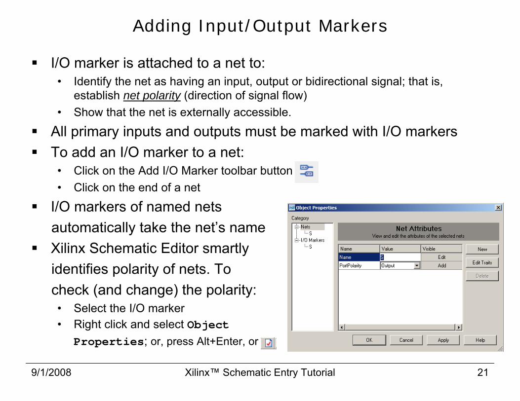
Adding Input/Output Markers
I/O marker is attached to a net to: • Identify the net as having an input, output or bidirectional signal; that is,
establish net polarity (direction of signal flow) • Show that the net is externally accessible.
All primary inputs and outputs must be marked with I/O markers To add an I/O marker to a net:• Click on the Add I/O Marker toolbar button • Click on the end of a net
I/O markers of named nets automatically take the net’s nameXilinx Schematic Editor smartly identifies polarity of nets. To check (and change) the polarity:• Select the I/O marker• Right click and select Object
Properties; or, press Alt+Enter, or
9/1/2008 Xilinx™ Schematic Entry Tutorial 22
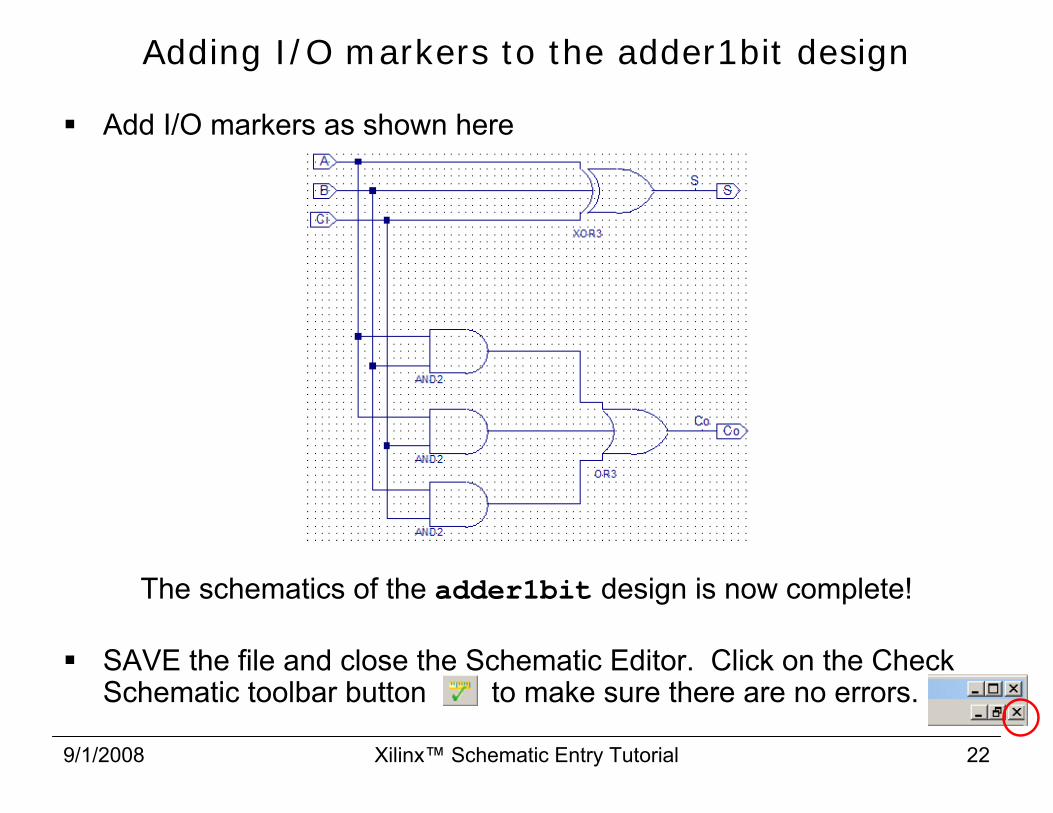
Adding I/O markers to the adder1bit design
Add I/O markers as shown here
The schematics of the adder1bit design is now complete!
SAVE the file and close the Schematic Editor. Click on the Check Schematic toolbar button to make sure there are no errors.

9/1/2008 Xilinx™ Schematic Entry Tutorial 23
Project Cleanup
Schematic filesSymbol filesTestbenchesVerilog filesUCF file(s)
Source files
Implementation filesReport files.bit file
Tool generated (derived) files
It is a good idea to perform project cleanup periodically, especially when things are not working the way you expect them to work!
9/1/2008 Xilinx™ Schematic Entry Tutorial 24
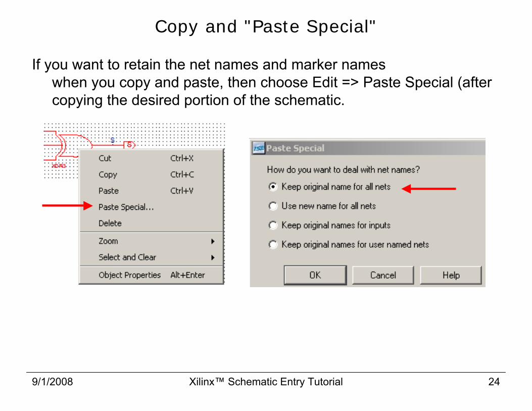
Copy and "Paste Special"
If you want to retain the net names and marker names when you copy and paste, then choose Edit => Paste Special (after copying the desired portion of the schematic.

9/1/2008 Xilinx™ Schematic Entry Tutorial 25
"Rename the Branch's Net" vs.
"Rename the Branch"
If you named some wire as S and then you later realize that it shouldhave been named S1.If you select that piece of wire (called Branch in Xilinx terminology),right-click, and select "Rename Net", then you have two choices:
Rename the Branch's NetRename the Branch
If you select, "Rename the Branch's Net" you are asking all wires in theentire (multi-sheet) schematic, which were previously named as S tobe renamed as S1.If that is not your intent, and if you just wanted to correct that singlepiece (called Branch), then you should select, "Rename the Branch".

9/1/2008 Xilinx™ Schematic Entry Tutorial 26
"Rename the Branch's Net" vs.
"Rename the Branch"
9/1/2008 Xilinx™ Schematic Entry Tutorial 27
Outline
Introduction to Xilinx ISE Project Navigator
Introduction to Xilinx ISE Schematics Entry Tool
Simulation Using Verilog Test Fixture in ModelSim XE
Creating Hierarchical Designs
Creating TOP Design to interface to Nexys2 board,implementing the design using ISE, and downloading the bit file using Adept
9/1/2008 Xilinx™ Schematic Entry Tutorial 28
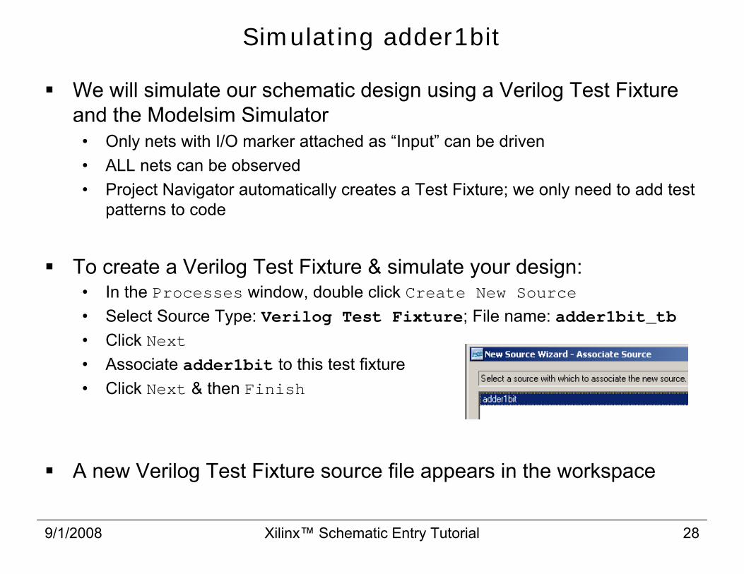
Simulating adder1bit
We will simulate our schematic design using a Verilog Test Fixture and the Modelsim Simulator• Only nets with I/O marker attached as “Input” can be driven• ALL nets can be observed• Project Navigator automatically creates a Test Fixture; we only need to add test
patterns to code
To create a Verilog Test Fixture & simulate your design:• In the Processes window, double click Create New Source• Select Source Type: Verilog Test Fixture; File name: adder1bit_tb• Click Next• Associate adder1bit to this test fixture• Click Next & then Finish
A new Verilog Test Fixture source file appears in the workspace

9/1/2008 Xilinx™ Schematic Entry Tutorial 29
Auto-generated Verilog Test Fixture
`timescale 1ns / 1ps• time unit is 1 nano second• resolution is 1 pico second
Module nameInput/Output declarations
• Test fixture code will drive inputs
Instantiating UUT• UUT = unit under test = adder1bit• format .port_name(signal_name)• port_name is the name of the i/o port of the
design under test• signal_name is the name of the test fixture
signal connected to this port
Delete lines 27-32 Do NOT delete line 33: the “endmodule” statementReplace lines 26-32 with test patterns given next …
deletekeep
Inputs to DUT
Outputs from DUT
Instantiation of DUT
Stimulus of DUT

9/1/2008 Xilinx™ Schematic Entry Tutorial 30
Adding Test Patterns
Code shown here adds 4 test patterns to the test fixture
Enter this code and complete it by adding the remaining 4 test patterns (total 2**3 = 8)
#10 => wait for 10 time units => 10ns
Once complete, SAVE the Verilog Test Fixture
9/1/2008 Xilinx™ Schematic Entry Tutorial 31
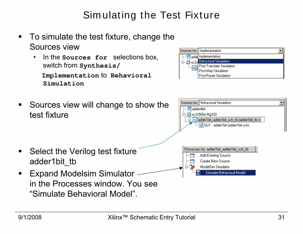
Simulating the Test Fixture
To simulate the test fixture, change the Sources view• In the Sources for selections box,
switch from Synthesis/Implementation to Behavioral Simulation
Sources view will change to show the test fixture
Select the Verilog test fixture adder1bit_tb Expand Modelsim Simulator in the Processes window. You see “Simulate Behavioral Model”.
9/1/2008 Xilinx™ Schematic Entry Tutorial 32
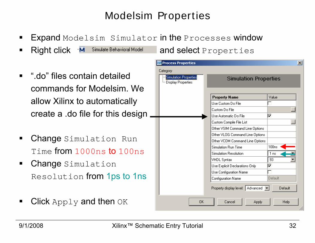
Modelsim Properties
Expand Modelsim Simulator in the Processes windowRight click and select Properties
“.do” files contain detailedcommands for Modelsim. We allow Xilinx to automatically create a .do file for this design
Change Simulation RunTime from 1000ns to 100nsChange SimulationResolution from 1ps to 1ns
Click Apply and then OK
9/1/2008 Xilinx™ Schematic Entry Tutorial 33
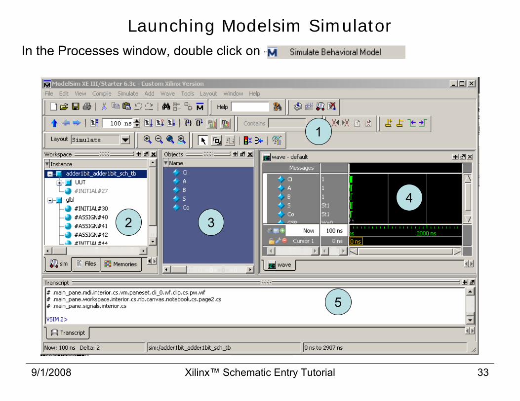
Launching Modelsim SimulatorIn the Processes window, double click on
1
2 3
4
5
9/1/2008 Xilinx™ Schematic Entry Tutorial 34
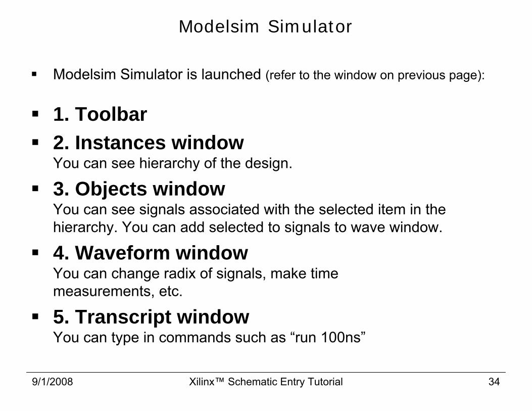
Modelsim Simulator
Modelsim Simulator is launched (refer to the window on previous page):
1. Toolbar2. Instances windowYou can see hierarchy of the design.
3. Objects windowYou can see signals associated with the selected item in the hierarchy. You can add selected to signals to wave window.
4. Waveform windowYou can change radix of signals, make timemeasurements, etc.
5. Transcript windowYou can type in commands such as “run 100ns”
9/1/2008 Xilinx™ Schematic Entry Tutorial 35
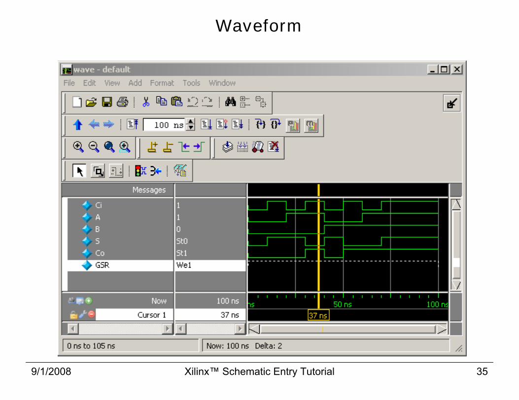
Waveform
9/1/2008 Xilinx™ Schematic Entry Tutorial 36
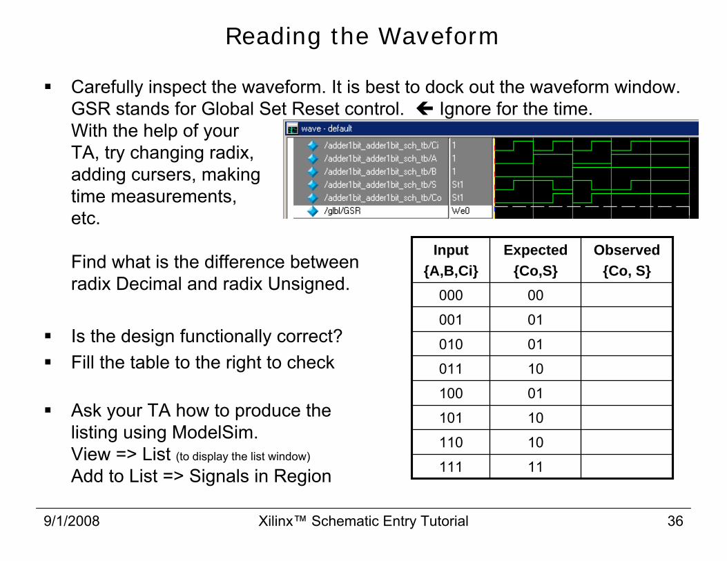
Reading the Waveform
Carefully inspect the waveform. It is best to dock out the waveform window. GSR stands for Global Set Reset control. Ignore for the time. With the help of your TA, try changing radix,adding cursers, makingtime measurements, etc.
Find what is the difference betweenradix Decimal and radix Unsigned.
Is the design functionally correct?Fill the table to the right to check
Ask your TA how to produce thelisting using ModelSim. View => List (to display the list window)
Add to List => Signals in Region 11
10
10
01
10
01
01
00
Expected {Co,S}
111
110
101
100
011
010
001
000
Observed{Co, S}
Input{A,B,Ci}

9/1/2008 Xilinx™ Schematic Entry Tutorial 37
Listing window
9/1/2008 Xilinx™ Schematic Entry Tutorial 38
Outline
Introduction to Xilinx ISE Project Navigator
Introduction to Xilinx ISE Schematics Entry Tool
Simulation Using Verilog Test Fixture in ModelSim XE
Creating Hierarchical Designs
Creating TOP Design to interface to Nexys2 board,implementing the design using ISE, and downloading the bit file using Adept

9/1/2008 Xilinx™ Schematic Entry Tutorial 39
Creating a Symbol
To create hierarchical design, basic building blocks have to be encapsulated into user-defined symbols that can be instantiated at the next higher (hierarchical) level
To create a symbol for adder1bit:• Open the schematic adder1bit.sch by double clicking it in the Sources window
• Click Tools→ Symbol Wizard
• On the Symbol Wizard – Source Page, under the
Pin Name Source choose Using Schematics: adder1bit• Leave shape set to Rectangle and click Next
9/1/2008 Xilinx™ Schematic Entry Tutorial 40
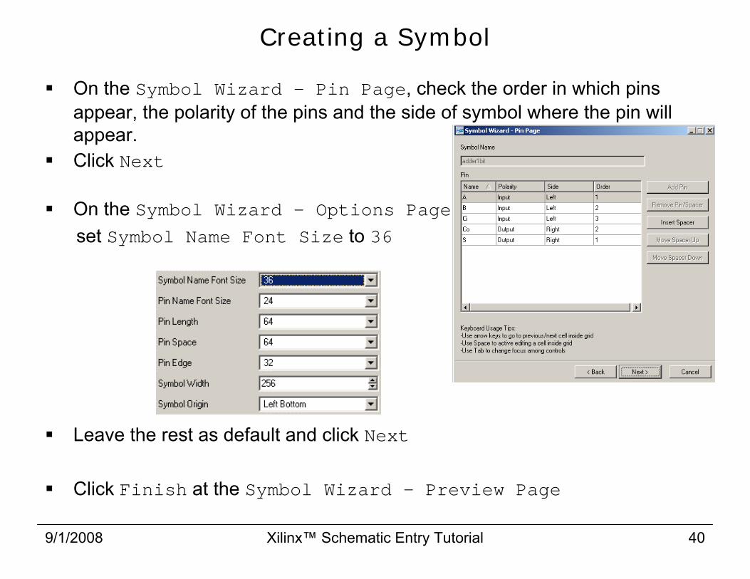
Creating a Symbol
On the Symbol Wizard – Pin Page, check the order in which pins appear, the polarity of the pins and the side of symbol where the pin will appear. Click Next
On the Symbol Wizard – Options Page, set Symbol Name Font Size to 36
Leave the rest as default and click Next
Click Finish at the Symbol Wizard – Preview Page

9/1/2008 Xilinx™ Schematic Entry Tutorial 41
Editing a Symbol
adder1bit.sym appears in the Schematic Editor workspace
You can edit any symbol using the drawing tools
We will not edit this symbol in this tutorial.However, note that, the small red squares representing the pins, and their labels arethe only significant items in the symbol.The rest of the symbol is just a graphicand can be mended as you like.
Close the Symbol and Schematic files.
Next, we create a 4-bit adder (adder4bit) using four 1-bit adder symbols (adder1bit)
Rectangle around a busis also just a graphic.
9/1/2008 Xilinx™ Schematic Entry Tutorial 42
Creating adder4bit
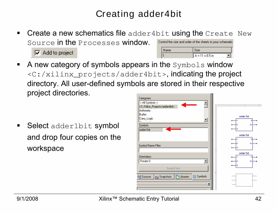
Create a new schematics file adder4bit using the Create New Source in the Processes window.
A new category of symbols appears in the Symbols window <C:/xilinx_projects/adder4bit>, indicating the project directory. All user-defined symbols are stored in their respective project directories.
Select adder1bit symboland drop four copies on the workspace

9/1/2008 Xilinx™ Schematic Entry Tutorial 43
Creating adder4bit
Connect adder1bit symbols to create a correct 4-bit adder
Connect Ci of the first adder1bit to the gnd symbol. Use the button
Name the A and B inputs of each adder1bit as A(0) through A(3) and B(0)through B(3), respectively
• to name multiple nets with names such as A(0), A(1), A(2),…, select Increase the namefrom the After naming the branch or net option in the Options window
Complete schematics as shown

9/1/2008 Xilinx™ Schematic Entry Tutorial 44
Adding Bus and Bus Taps
To create signals A, B and S as buses, add three dangling nets (neither end connected to any pin) and name them A(3:0), B(3:0) and S(3:0). This creates three buses
These three nets will appear as thicker lines than ordinary (1-bit) wires as they are buses
Then, connect I/O markers to each of these buses and one to Cout
Completed schematics is shown here
9/1/2008 Xilinx™ Schematic Entry Tutorial 45
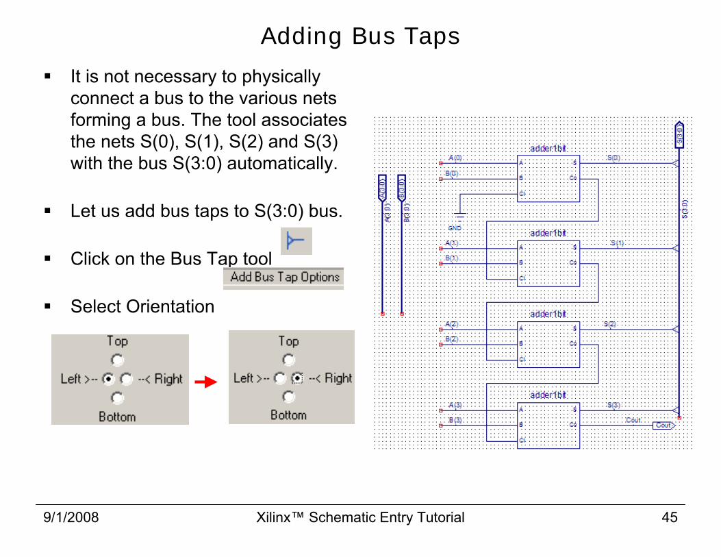
Adding Bus Taps
It is not necessary to physically connect a bus to the various nets forming a bus. The tool associates the nets S(0), S(1), S(2) and S(3) with the bus S(3:0) automatically.
Let us add bus taps to S(3:0) bus.
Click on the Bus Tap tool
Select Orientation

9/1/2008 Xilinx™ Schematic Entry Tutorial 46
Labeling instances may be very beneficial
The four instances of the adder1bit in the adder4bit design appear with machine generated names as seen on the side.
Also, if you simulate the adder4bit design in ModelSim, the four instances of the adder1bit appear with machine generated names as seen on the side.
The hierarchical names of nodes inside an instance in ModelSimlook like
After labeling the instances as FA0, FA1, FA2, and FA3, the same looks like
9/1/2008 Xilinx™ Schematic Entry Tutorial 47
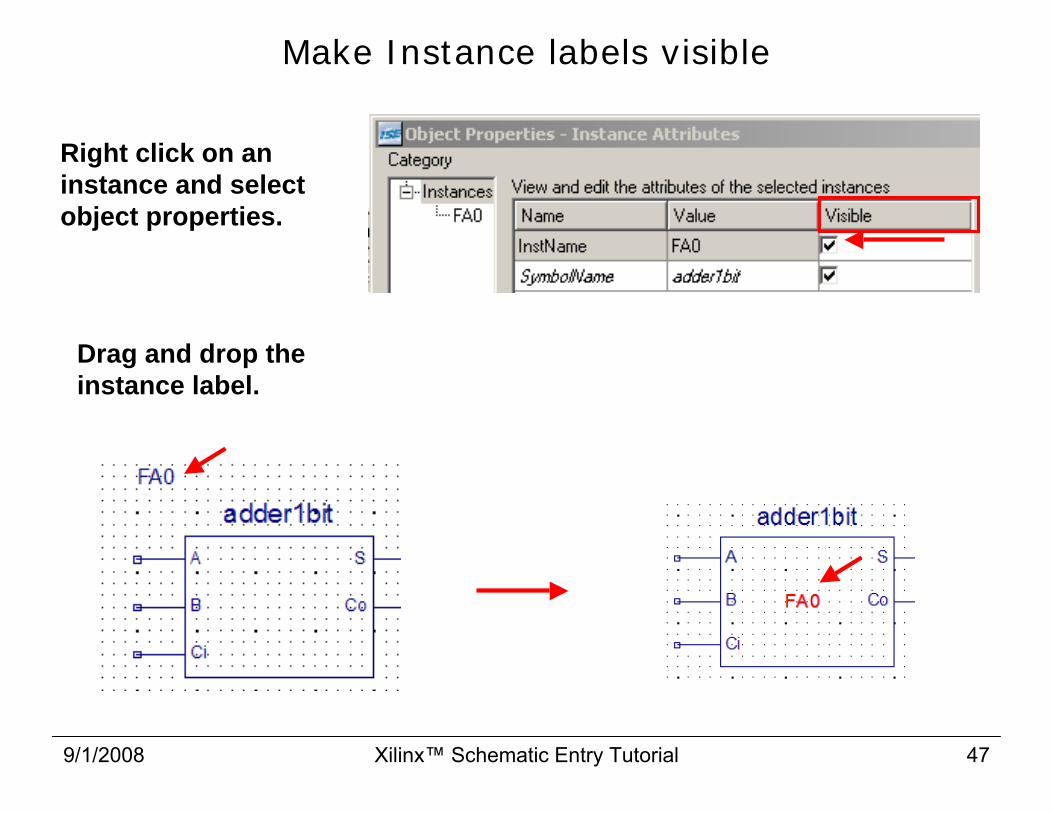
Make Instance labels visible
Right click on an instance and select object properties.
Drag and drop the instance label.
9/1/2008 Xilinx™ Schematic Entry Tutorial 48
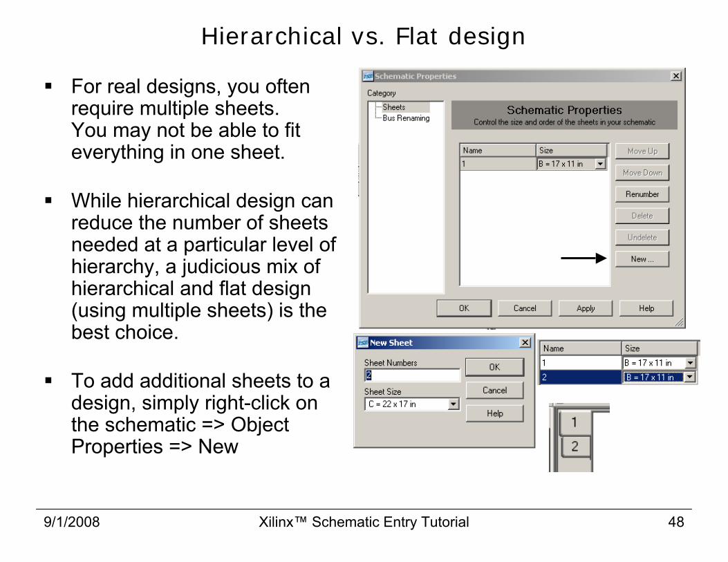
Hierarchical vs. Flat design
For real designs, you often require multiple sheets.You may not be able to fit everything in one sheet.
While hierarchical design can reduce the number of sheets needed at a particular level of hierarchy, a judicious mix of hierarchical and flat design (using multiple sheets) is the best choice.
To add additional sheets to a design, simply right-click on the schematic => Object Properties => New
9/1/2008 Xilinx™ Schematic Entry Tutorial 49
Outline
Introduction to Xilinx ISE Project Navigator
Introduction to Xilinx ISE Schematics Entry Tool
Simulation Using Verilog Test Fixture in ModelSim XE
Creating Hierarchical Designs
Creating TOP Design to interface to Nexys2 board,implementing the design using ISE, and downloading the bit file using Adept
Very briefly!
9/1/2008 Xilinx™ Schematic Entry Tutorial 50
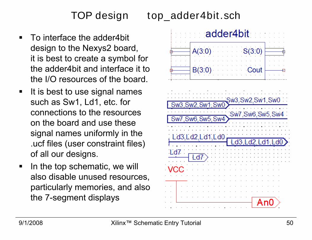
TOP design top_adder4bit.sch
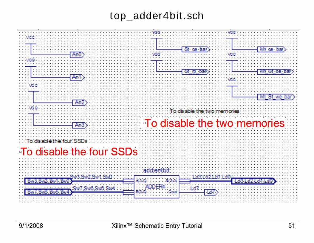
To interface the adder4bit design to the Nexys2 board, it is best to create a symbol for the adder4bit and interface it to the I/O resources of the board.It is best to use signal names such as Sw1, Ld1, etc. for connections to the resources on the board and use these signal names uniformly in the .ucf files (user constraint files) of all our designs.In the top schematic, we will also disable unused resources, particularly memories, and also the 7-segment displays
9/1/2008 Xilinx™ Schematic Entry Tutorial 51
top_adder4bit.sch
9/1/2008 Xilinx™ Schematic Entry Tutorial 52
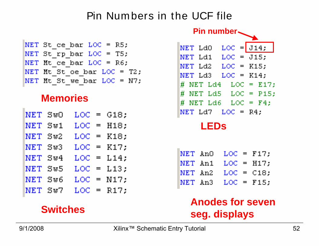
Pin Numbers in the UCF file
Memories
Switches
LEDs
Anodes for seven seg. displays
Pin number
9/1/2008 Xilinx™ Schematic Entry Tutorial 53
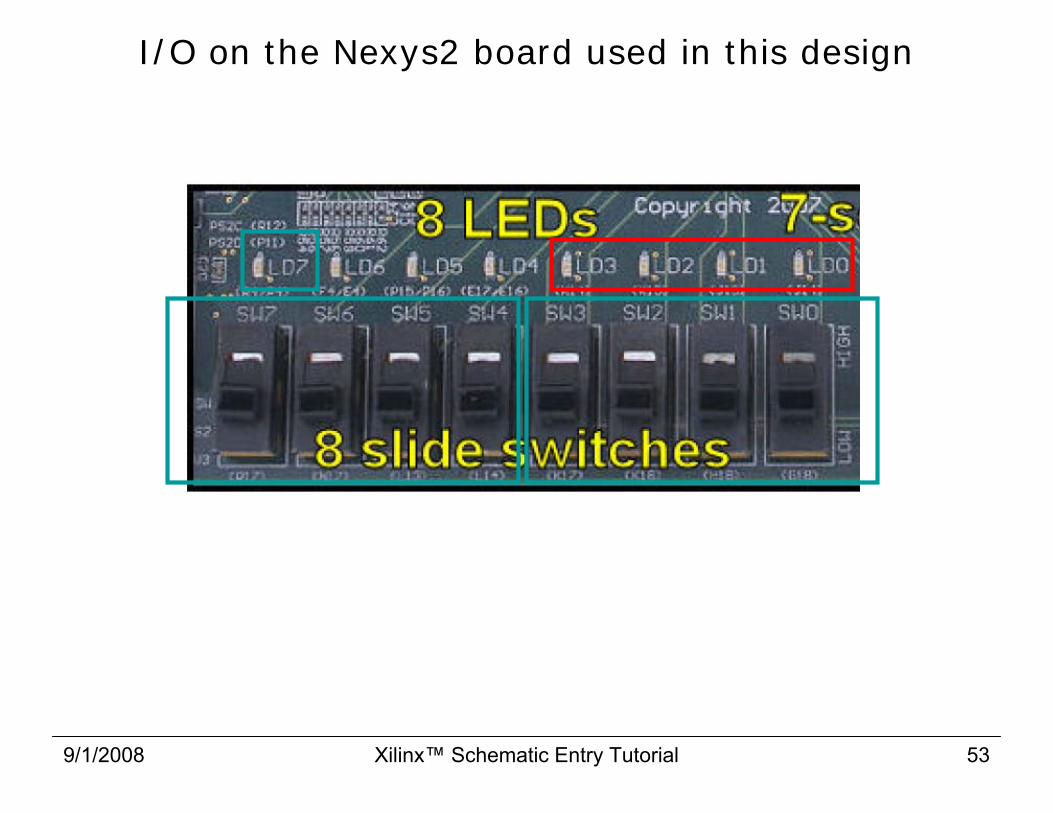
I/O on the Nexys2 board used in this design

9/1/2008 Xilinx™ Schematic Entry Tutorial 54
Download the .bit file (top_adder4bit.bit) to Nexys2
Setup jumpers on Nexys2 board for USB-powering arrangement.
Connect Nexys2 to the PC using USB cable.
Invoke Adept Exporter.
Initialize Chain. Bypass the flash memory chip.
Add the top_adder4bit.bit file.
Program.

9/1/2008 Xilinx™ Schematic Entry Tutorial 55
References
For help on ISE topics, Help => Help topics
Allow blocked content.Use Index search toget help.
For information on functional elements available in the symbol library such as counter cb8ce
Help => Software Manuals = > libraries guide on the left panel =>Spartan-3 Libraries Guide for Schematic Designs => Functional Categories => Counter => CB8CE

9/1/2008 Xilinx™ Schematic Entry Tutorial 56
Congratulations on your Finish!
This is me!
and, that is you