zl2102 datasheet - intersil.com vsen sw bst vra vr vdds vddp en v2p5 mgn sgnd pgnd cfg ss epad...
TRANSCRIPT

FN8440Rev 2.00
November 20, 2014
ZL21026A Digital Integrated Synchronous Step-Down DC/DC Regulator with Auto Compensation
DATASHEET
The ZL2102 is an integrated digital power regulator with auto compensation and power management functions in a small package, resulting in a flexible and integrated solution, which can be configured using the PowerNavigator™ graphical user interface. This synchronous buck converter operates from a 4.5V to 14V input supply and provides from 0.54V to 5.5V output voltage at up to 6A.
The ZL2102 can be configured for most applications using only hardware pin straps to adjust switching frequency, output voltage, UVLO, soft-start ramp/delay settings, sequencing options, and SMBus address. For more advanced configurations, the ZL2102 supports over 70 PMBus commands. Output voltage/current is factory calibrated.
Internal synchronous power MOSFETs enable the ZL2102 to deliver continuous loads up to 6A with high efficiency. An internal Schottky bootstrap diode reduces discrete component count. The ZL2102 also supports phase spreading to reduce system input capacitance.
The ZL2102 uses the SMBus™ with PMBus™ protocol for communication with a host controller and the Intersil's proprietary Digital-DC™ bus for interoperability between other Intersil devices.
Features• Integrated MOSFET switches
• 6A continuous output current
• Adjustable 0.54V to 5.5V output range
• 4.5V to 14V input range
• Up to 90% efficiency
• Auto compensation for fast transient response
• SMBus compliant serial interface
• Snapshot™ parametric capture
• Internal nonvolatile memory
• Small footprint QFN package (6mmx6mm)
Applications• Servers/storage equipment
• Telecom/datacom equipment
• Power supplies (memory, DSP, ASIC, FPGA)
Related Literature• AN2010 "Thermal and Layout Guidelines for Digital-DC™
Products"
• AN2035 "Compensation Using CompZL™"
• TB389 "PCB Land Pattern and Surface Mount Guidelines for QFN Packages"
FIGURE 1. TYPICAL APPLICATION DIAGRAM
VIN
12V
SMBus
DDC Bus
CB
0.1µF
10µF
COUT
200µF
LOUT
2.2µH
CIN
100µF
VSET
SA
SCL
SDA
SALRT
FC
PG
SYNC
DGND
ZL2102
VSEN
SW
BST
VRA
VR
VDDS
VDDP
EN
V2P5
MGN
SGND
PGND
CFG
SS ePAD
4.7µF
DDC
VOUT
3.3V6A
4.7µF
HARDWARECONFIG
HARDWARE CONTROL
INTERFACE
FN8440 Rev 2.00 Page 1 of 58November 20, 2014

ZL2102
Table of ContentsPin Configuration. . . . . . . . . . . . . . . . . . . . . . . . . . . . . . . . . . . . . . . . . . . . . . . . . . . . . . . . . . . . . . . . . . . . . . . . . . . . . . . . . . . . . . . . . . . . 3
Pin Description. . . . . . . . . . . . . . . . . . . . . . . . . . . . . . . . . . . . . . . . . . . . . . . . . . . . . . . . . . . . . . . . . . . . . . . . . . . . . . . . . . . . . . . . . . . . . . 4
Ordering Information . . . . . . . . . . . . . . . . . . . . . . . . . . . . . . . . . . . . . . . . . . . . . . . . . . . . . . . . . . . . . . . . . . . . . . . . . . . . . . . . . . . . . . . . 4
Absolute Maximum Ratings . . . . . . . . . . . . . . . . . . . . . . . . . . . . . . . . . . . . . . . . . . . . . . . . . . . . . . . . . . . . . . . . . . . . . . . . . . . . . . . . . . . 5
Thermal Information . . . . . . . . . . . . . . . . . . . . . . . . . . . . . . . . . . . . . . . . . . . . . . . . . . . . . . . . . . . . . . . . . . . . . . . . . . . . . . . . . . . . . . . . . 5
Recommended Operating Conditions . . . . . . . . . . . . . . . . . . . . . . . . . . . . . . . . . . . . . . . . . . . . . . . . . . . . . . . . . . . . . . . . . . . . . . . . . . 5
Electrical Specifications . . . . . . . . . . . . . . . . . . . . . . . . . . . . . . . . . . . . . . . . . . . . . . . . . . . . . . . . . . . . . . . . . . . . . . . . . . . . . . . . . . . . . 5
Typical Performance Curves . . . . . . . . . . . . . . . . . . . . . . . . . . . . . . . . . . . . . . . . . . . . . . . . . . . . . . . . . . . . . . . . . . . . . . . . . . . . . . . . . . 7
Digital-DC Architecture Overview . . . . . . . . . . . . . . . . . . . . . . . . . . . . . . . . . . . . . . . . . . . . . . . . . . . . . . . . . . . . . . . . . . . . . . . . . . . . . . 8
Power Conversion Overview. . . . . . . . . . . . . . . . . . . . . . . . . . . . . . . . . . . . . . . . . . . . . . . . . . . . . . . . . . . . . . . . . . . . . . . . . . . . . . . . . . . 9
Power Management Overview . . . . . . . . . . . . . . . . . . . . . . . . . . . . . . . . . . . . . . . . . . . . . . . . . . . . . . . . . . . . . . . . . . . . . . . . . . . . . . . . . 9Functional Description and Configuration . . . . . . . . . . . . . . . . . . . . . . . . . . . . . . . . . . . . . . . . . . . . . . . . . . . . . . . . . . . . . . . . . . . . . . . . . . . . .9SMBus Device Address Selection (SA) . . . . . . . . . . . . . . . . . . . . . . . . . . . . . . . . . . . . . . . . . . . . . . . . . . . . . . . . . . . . . . . . . . . . . . . . . . . . . . 10Output Voltage and VOUT_MAX Selection (VSET) . . . . . . . . . . . . . . . . . . . . . . . . . . . . . . . . . . . . . . . . . . . . . . . . . . . . . . . . . . . . . . . . . . . . . 11Automatic Loop Compensation (FC) . . . . . . . . . . . . . . . . . . . . . . . . . . . . . . . . . . . . . . . . . . . . . . . . . . . . . . . . . . . . . . . . . . . . . . . . . . . . . . . . 11Synchronization and Sequencing Configuration Settings (CFG) . . . . . . . . . . . . . . . . . . . . . . . . . . . . . . . . . . . . . . . . . . . . . . . . . . . . . . . . . 12Switching Frequency Setting (SYNC) . . . . . . . . . . . . . . . . . . . . . . . . . . . . . . . . . . . . . . . . . . . . . . . . . . . . . . . . . . . . . . . . . . . . . . . . . . . . . . . . 12Soft-Start and UVLO Settings (SS) . . . . . . . . . . . . . . . . . . . . . . . . . . . . . . . . . . . . . . . . . . . . . . . . . . . . . . . . . . . . . . . . . . . . . . . . . . . . . . . . . . 13Start-up Procedure. . . . . . . . . . . . . . . . . . . . . . . . . . . . . . . . . . . . . . . . . . . . . . . . . . . . . . . . . . . . . . . . . . . . . . . . . . . . . . . . . . . . . . . . . . . . . . . 13Power-Good . . . . . . . . . . . . . . . . . . . . . . . . . . . . . . . . . . . . . . . . . . . . . . . . . . . . . . . . . . . . . . . . . . . . . . . . . . . . . . . . . . . . . . . . . . . . . . . . . . . . 14
Power Management Function Description. . . . . . . . . . . . . . . . . . . . . . . . . . . . . . . . . . . . . . . . . . . . . . . . . . . . . . . . . . . . . . . . . . . . . . 14Input Undervoltage Lockout . . . . . . . . . . . . . . . . . . . . . . . . . . . . . . . . . . . . . . . . . . . . . . . . . . . . . . . . . . . . . . . . . . . . . . . . . . . . . . . . . . . . . . . 14Output Overvoltage Protection. . . . . . . . . . . . . . . . . . . . . . . . . . . . . . . . . . . . . . . . . . . . . . . . . . . . . . . . . . . . . . . . . . . . . . . . . . . . . . . . . . . . . 14Output Prebias Protection . . . . . . . . . . . . . . . . . . . . . . . . . . . . . . . . . . . . . . . . . . . . . . . . . . . . . . . . . . . . . . . . . . . . . . . . . . . . . . . . . . . . . . . . 14Output Overcurrent Protection . . . . . . . . . . . . . . . . . . . . . . . . . . . . . . . . . . . . . . . . . . . . . . . . . . . . . . . . . . . . . . . . . . . . . . . . . . . . . . . . . . . . . 15Thermal Overload Protection . . . . . . . . . . . . . . . . . . . . . . . . . . . . . . . . . . . . . . . . . . . . . . . . . . . . . . . . . . . . . . . . . . . . . . . . . . . . . . . . . . . . . . 15Voltage Margining . . . . . . . . . . . . . . . . . . . . . . . . . . . . . . . . . . . . . . . . . . . . . . . . . . . . . . . . . . . . . . . . . . . . . . . . . . . . . . . . . . . . . . . . . . . . . . . 15Digital-DC Bus . . . . . . . . . . . . . . . . . . . . . . . . . . . . . . . . . . . . . . . . . . . . . . . . . . . . . . . . . . . . . . . . . . . . . . . . . . . . . . . . . . . . . . . . . . . . . . . . . . 15Phase Spreading . . . . . . . . . . . . . . . . . . . . . . . . . . . . . . . . . . . . . . . . . . . . . . . . . . . . . . . . . . . . . . . . . . . . . . . . . . . . . . . . . . . . . . . . . . . . . . . . 15Output Sequencing . . . . . . . . . . . . . . . . . . . . . . . . . . . . . . . . . . . . . . . . . . . . . . . . . . . . . . . . . . . . . . . . . . . . . . . . . . . . . . . . . . . . . . . . . . . . . . 16Fault Spreading . . . . . . . . . . . . . . . . . . . . . . . . . . . . . . . . . . . . . . . . . . . . . . . . . . . . . . . . . . . . . . . . . . . . . . . . . . . . . . . . . . . . . . . . . . . . . . . . . 16Monitoring via SMBus . . . . . . . . . . . . . . . . . . . . . . . . . . . . . . . . . . . . . . . . . . . . . . . . . . . . . . . . . . . . . . . . . . . . . . . . . . . . . . . . . . . . . . . . . . . . 16Nonvolatile Memory . . . . . . . . . . . . . . . . . . . . . . . . . . . . . . . . . . . . . . . . . . . . . . . . . . . . . . . . . . . . . . . . . . . . . . . . . . . . . . . . . . . . . . . . . . . . . 16Snapshot™ Parametric Capture . . . . . . . . . . . . . . . . . . . . . . . . . . . . . . . . . . . . . . . . . . . . . . . . . . . . . . . . . . . . . . . . . . . . . . . . . . . . . . . . . . . 16Power Train Component Selection . . . . . . . . . . . . . . . . . . . . . . . . . . . . . . . . . . . . . . . . . . . . . . . . . . . . . . . . . . . . . . . . . . . . . . . . . . . . . . . . . 17Design Goal Trade-offs . . . . . . . . . . . . . . . . . . . . . . . . . . . . . . . . . . . . . . . . . . . . . . . . . . . . . . . . . . . . . . . . . . . . . . . . . . . . . . . . . . . . . . . . . . . 17Inductor Selection . . . . . . . . . . . . . . . . . . . . . . . . . . . . . . . . . . . . . . . . . . . . . . . . . . . . . . . . . . . . . . . . . . . . . . . . . . . . . . . . . . . . . . . . . . . . . . . 17Output Capacitor Selection. . . . . . . . . . . . . . . . . . . . . . . . . . . . . . . . . . . . . . . . . . . . . . . . . . . . . . . . . . . . . . . . . . . . . . . . . . . . . . . . . . . . . . . . 17Input Capacitor. . . . . . . . . . . . . . . . . . . . . . . . . . . . . . . . . . . . . . . . . . . . . . . . . . . . . . . . . . . . . . . . . . . . . . . . . . . . . . . . . . . . . . . . . . . . . . . . . . 18
PCB Layout Recommendation . . . . . . . . . . . . . . . . . . . . . . . . . . . . . . . . . . . . . . . . . . . . . . . . . . . . . . . . . . . . . . . . . . . . . . . . . . . . . . . . 18
PMBus Command Summary . . . . . . . . . . . . . . . . . . . . . . . . . . . . . . . . . . . . . . . . . . . . . . . . . . . . . . . . . . . . . . . . . . . . . . . . . . . . . . . . . . 19PMBus Data Formats . . . . . . . . . . . . . . . . . . . . . . . . . . . . . . . . . . . . . . . . . . . . . . . . . . . . . . . . . . . . . . . . . . . . . . . . . . . . . . . . . . . . . . . . . . . . 21PMBus Command Detail. . . . . . . . . . . . . . . . . . . . . . . . . . . . . . . . . . . . . . . . . . . . . . . . . . . . . . . . . . . . . . . . . . . . . . . . . . . . . . . . . . . . . . . . . . 22
Revision History. . . . . . . . . . . . . . . . . . . . . . . . . . . . . . . . . . . . . . . . . . . . . . . . . . . . . . . . . . . . . . . . . . . . . . . . . . . . . . . . . . . . . . . . . . . . 57
About Intersil . . . . . . . . . . . . . . . . . . . . . . . . . . . . . . . . . . . . . . . . . . . . . . . . . . . . . . . . . . . . . . . . . . . . . . . . . . . . . . . . . . . . . . . . . . . . . . 57
Package Outline Drawing . . . . . . . . . . . . . . . . . . . . . . . . . . . . . . . . . . . . . . . . . . . . . . . . . . . . . . . . . . . . . . . . . . . . . . . . . . . . . . . . . . . . 58
FN8440 Rev 2.00 Page 2 of 58November 20, 2014

ZL2102
Pin ConfigurationZL2102
(36 LD 6x6 QFN)TOP VIEW
FIGURE 2. BLOCK DIAGRAM
VSET
SA
SCL
SDA
SALRT
FC
PG
SYNC
DGND
SW
SW
SW
SW
SW
PGND
VDDP
SW
BST
VR
A
VR
VD
DS
VD
DP
VD
DP
EN
V2
P5
MG
N
VS
EN
SG
ND
PG
ND
PG
ND
PG
ND
PG
ND
CF
G
DN
C
SS
DD
C
EXPOSED PADDLE
CONNECT TO SGND
27
26
25
24
23
22
21
36
35
34
33
32
10
11
12
13
14
1
2
3
4
5
6
7
8
9
20
19
15
31
16
30
17
18
29
28
FN8440 Rev 2.00 Page 3 of 58November 20, 2014
ZL2102
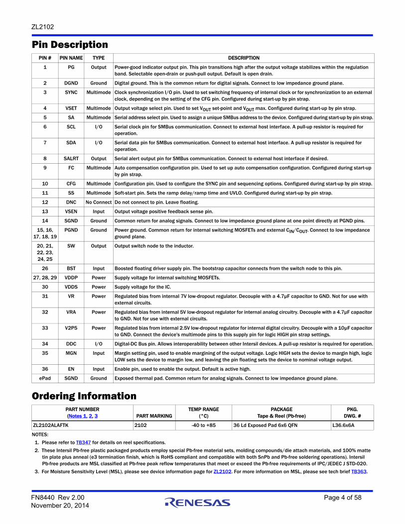
Pin DescriptionPIN # PIN NAME TYPE DESCRIPTION
1 PG Output Power-good indicator output pin. This pin transitions high after the output voltage stabilizes within the regulation band. Selectable open-drain or push-pull output. Default is open drain.
2 DGND Ground Digital ground. This is the common return for digital signals. Connect to low impedance ground plane.
3 SYNC Multimode Clock synchronization I/O pin. Used to set switching frequency of internal clock or for synchronization to an external clock, depending on the setting of the CFG pin. Configured during start-up by pin strap.
4 VSET Multimode Output voltage select pin. Used to set VOUT set-point and VOUT max. Configured during start-up by pin strap.
5 SA Multimode Serial address select pin. Used to assign a unique SMBus address to the device. Configured during start-up by pin strap.
6 SCL I/O Serial clock pin for SMBus communication. Connect to external host interface. A pull-up resistor is required for operation.
7 SDA I/O Serial data pin for SMBus communication. Connect to external host interface. A pull-up resistor is required for operation.
8 SALRT Output Serial alert output pin for SMBus communication. Connect to external host interface if desired.
9 FC Multimode Auto compensation configuration pin. Used to set up auto compensation configuration. Configured during start-up by pin strap.
10 CFG Multimode Configuration pin. Used to configure the SYNC pin and sequencing options. Configured during start-up by pin strap.
11 SS Multimode Soft-start pin. Sets the ramp delay/ramp time and UVLO. Configured during start-up by pin strap.
12 DNC No Connect Do not connect to pin. Leave floating.
13 VSEN Input Output voltage positive feedback sense pin.
14 SGND Ground Common return for analog signals. Connect to low impedance ground plane at one point directly at PGND pins.
15, 16, 17, 18, 19
PGND Ground Power ground. Common return for internal switching MOSFETs and external CIN/COUT. Connect to low impedance ground plane.
20, 21, 22, 23, 24, 25
SW Output Output switch node to the inductor.
26 BST Input Boosted floating driver supply pin. The bootstrap capacitor connects from the switch node to this pin.
27, 28, 29 VDDP Power Supply voltage for internal switching MOSFETs.
30 VDDS Power Supply voltage for the IC.
31 VR Power Regulated bias from internal 7V low-dropout regulator. Decouple with a 4.7μF capacitor to GND. Not for use with external circuits.
32 VRA Power Regulated bias from internal 5V low-dropout regulator for internal analog circuitry. Decouple with a 4.7μF capacitor to GND. Not for use with external circuits.
33 V2P5 Power Regulated bias from internal 2.5V low-dropout regulator for internal digital circuitry. Decouple with a 10µF capacitor to GND. Connect the device's multimode pins to this supply pin for logic HIGH pin strap settings.
34 DDC I/O Digital-DC Bus pin. Allows interoperability between other Intersil devices. A pull-up resistor is required for operation.
35 MGN Input Margin setting pin, used to enable margining of the output voltage. Logic HIGH sets the device to margin high, logic LOW sets the device to margin low, and leaving the pin floating sets the device to nominal voltage output.
36 EN Input Enable pin, used to enable the output. Default is active high.
ePad SGND Ground Exposed thermal pad. Common return for analog signals. Connect to low impedance ground plane.
Ordering InformationPART NUMBER(Notes 1, 2, 3 PART MARKING
TEMP RANGE(°C)
PACKAGETape & Reel (Pb-free)
PKG. DWG. #
ZL2102ALAFTK 2102 -40 to +85 36 Ld Exposed Pad 6x6 QFN L36.6x6A
NOTES:
1. Please refer to TB347 for details on reel specifications.
2. These Intersil Pb-free plastic packaged products employ special Pb-free material sets, molding compounds/die attach materials, and 100% matte tin plate plus anneal (e3 termination finish, which is RoHS compliant and compatible with both SnPb and Pb-free soldering operations). Intersil Pb-free products are MSL classified at Pb-free peak reflow temperatures that meet or exceed the Pb-free requirements of IPC/JEDEC J STD-020.
3. For Moisture Sensitivity Level (MSL), please see device information page for ZL2102. For more information on MSL, please see tech brief TB363.
FN8440 Rev 2.00 Page 4 of 58November 20, 2014
ZL2102
Absolute Maximum Ratings Thermal InformationDC Supply Voltage for VDDP, VDDS Pins . . . . . . . . . . . . . . . . . . -0.3V to 17VHigh-Side Supply Voltage for BST Pin. . . . . . . . . . . . . . . . . . . . -0.3V to 25VHigh-Side Boost Voltage for BST, SW Pins. . . . . . . . . . . . . . . . . . -0.3V to 8VInternal MOSFET Reference for VR Pin . . . . . . . . . . . . . . . . . . -0.3V to 8.5VInternal Analog Reference for VRA Pin . . . . . . . . . . . . . . . . . . -0.3V to 6.5VInternal 2.5V Reference for V2P5 Pin . . . . . . . . . . . . . . . . . . . . . -0.3V to 3VLogic I/O Voltage for EN, CFG, DDC, FC, MGN, PG, SDA, SCL,SA, SALRT, SS, SYNC, VSET, VSEN Pins . . . . . . . . . . . . . . . . . . -0.3V to 6.5VGround Differential for DGND - SGND, PGND - SGND Pins . . . . . . . . ±0.3VMOSFET Drive Reference Current for VR Pin Internal Bias Usage . . . 20mASwitch Node Current for SW Pin Peak (Sink Or Source) . . . . . . . . . . . . 10AESD Rating
Human Body Model (Tested per JESD22-A114F) . . . . . . . . . . . . . . . . 2kVCharged Device Model (Tested per JESD22-C101D) . . . . . . . . . . . . 750VMachine Model (Tested per JESD22-A115-A) . . . . . . . . . . . . . . . . . . 200V
Latch-up (Tested per JESD78C; Class 2, Level A) . . . . . . . . . . . . . . . 100mA
Thermal Resistance (Typical) JA (°C/W) JC (°C/W)36 Ld QFN Package (Notes 4, 5) . . . . . . . . 28 1.7
Junction Temperature . . . . . . . . . . . . . . . . . . . . . . . . . . . . .-55°C to +150°CStorage Temperature Range. . . . . . . . . . . . . . . . . . . . . . . .-55°C to +150°CDissipation Limits (Note 6)
TA = +25°C . . . . . . . . . . . . . . . . . . . . . . . . . . . . . . . . . . . . . . . . . . . . . . 3.5WTA = +55°C . . . . . . . . . . . . . . . . . . . . . . . . . . . . . . . . . . . . . . . . . . . . . . 2.5WTA = +85°C . . . . . . . . . . . . . . . . . . . . . . . . . . . . . . . . . . . . . . . . . . . . . . 1.4W
Pb-Free Reflow Profile . . . . . . . . . . . . . . . . . . . . . . . . . . . . . . . . . . see TB493
Recommended Operating ConditionsInput Supply Voltage Range, VDDP, VDDS (see Figure 10 on page 10)VDDS tied to VR, VRA. . . . . . . . . . . . . . . . . . . . . . . . . . . . . . . . . . 4.5V to 5.5VVDDS tied to VR, VRA Floating . . . . . . . . . . . . . . . . . . . . . . . . . . 5.5V to 7.5VVR, VRA Floating. . . . . . . . . . . . . . . . . . . . . . . . . . . . . . . . . . . . . . .7.5V to 14VOutput Voltage Range, VOUT (Note 7) . . . . . . . . . . . . . . . . . . . 0.54V to 5.5VOperating Junction Temperature Range, TJ. . . . . . . . . . . .-40°C to +125°C
CAUTION: Do not operate at or near the maximum ratings listed for extended periods of time. Exposure to such conditions may adversely impact productreliability and result in failures not covered by warranty.
NOTES:
4. JA is measured in free air with the device mounted on a multi-layer FR4 test board and the exposed metal pad soldered to a low impedance ground plane using multiple vias.
5. For JC, the "case temp" location is the center of the exposed metal pad on the package underside.
6. Thermal impedance is dependent upon PCB layout.
7. Includes margin limits.
Electrical Specifications VDDP = VDDS = 12V, TA = -40°C to +85°C unless otherwise noted (Note 9). Typical values are at TA = +25°C. Boldface limits apply across the operating temperature range, -40°C to +85°C.
PARAMETER TEST CONDITIONSMIN
(Note 8) TYPMAX
(Note 8) UNIT
IC INPUT AND BIAS SUPPLY CHARACTERISTICS
IDD Supply Current fSW = 200kHz, no load – 15 25 mA
fSW = 1MHz, no load – 15 30 mA
IDD Shutdown Current EN = 0 V, no SMBus activity, low power standby mode
– 0.6 1 mA
VR Reference Output Voltage VDD > 8V, IVR < 10mA 6.5 7.0 7.5 V
VRA Reference Output Voltage VDD > 5.5V, IVRA < 20mA 4.5 5.1 5.5 V
V2P5 Reference Output Voltage IV2P5 < 20mA 2.25 2.5 2.75 V
OUTPUT CHARACTERISTICS
Output Current IRMS, continuous – – 6 A
Peak (Note 11) – – 9 A
Output Voltage Adjustment Range (Note 10) VIN > VOUT 0.6 – 5.0 V
Output Voltage Set-point Accuracy Across line, load, temperature variation -1 – 1 %
Output Voltage Set-point Resolution Set using PMBus command – ±2 – mV
VSEN Input Bias Current VSEN = 5.5V – 110 200 µA
FN8440 Rev 2.00 Page 5 of 58November 20, 2014

ZL2102
LOGIC INPUT/OUTPUT CHARACTERISTICS
Logic Input Leakage Current Logic I/O - multimode pins -250 – 250 nA
Logic Input Low, VIL – – 0.8 V
Logic input Open (N/C) Multimode logic pins – 1.4 – V
Logic Input High, VIH 2.0 – – V
Logic Output Low, VOL IOL ≤ 4mA – – 0.4 V
Logic Output High, VOH IOH ≥ -2mA 2.25 – – V
OSCILLATOR AND SWITCHING CHARACTERISTICS
Switching Frequency Range 200 - 1000 kHz
Switching Frequency Set-Point Accuracy -5 - 5 %
PWM Duty Cycle 0 - 95 %
Minimum SYNC Pulse Width 150 - - ns
Input Clock Frequency Drift Tolerance External clock source -13 - 13 %
rDS(ON) of High-Side N-channel FETs ISW = 6A, VGS = 6.5V - 60 85 mΩ
rDS(ON) of Low-Side N-channel FETs ISW = 6A, VGS = 12V - 43 65 mΩ
SMBUS CHARACTERISTICS
SMBus Clock Rate - 100 - kHz
Wait Time Between Consecutive Commands 2 - - ms
POWER MANAGEMENT
SOFT-START RAMP CHARACTERISTICS
Soft-Start Ramp Delay Range Set using PMBus command 5 - 30000 ms
Soft-Start Ramp Delay Accuracy Turn-on, turn off delay -1 ±1 +5 ms
Soft-Start Ramp Duration Range Set using PMBus command 5 - 200 ms
Soft-Start Ramp Duration Accuracy Turn-on, turn off delay - ±1 - ms
POWER-GOOD
Power-Good VOUT Threshold Factory default - 90 - % VOUT
Power-Good VOUT Hysteresis Factory default - 5 - %
Power-Good DelayApplies to Turn-On Only (Low-to-High transition)
Factory default - 1 - ms
Set using PMBus command 1 30000 ms
MONITORING AND FAULT MANAGEMENT
INPUT VOLTAGE MONITOR AND FAULT DETECTION
VIN Monitor Accuracy -150 - 150 mV
VIN UVLO Threshold Range Set using PMBus command 4.5 - 16 V
UVLO Hysteresis Factory default - 3 - %
Electrical Specifications VDDP = VDDS = 12V, TA = -40°C to +85°C unless otherwise noted (Note 9). Typical values are at TA = +25°C. Boldface limits apply across the operating temperature range, -40°C to +85°C. (Continued)
PARAMETER TEST CONDITIONSMIN
(Note 8) TYPMAX
(Note 8) UNIT
FN8440 Rev 2.00 Page 6 of 58November 20, 2014
ZL2102
OUTPUT VOLTAGE MONITOR AND FAULT DETECTION
VOUT Undervoltage Hysteresis Factory default - 5 - % VOUT
VOUT UV/OV Fault Response Delay - 30 - µs
OUTPUT CURRENT SENSE MONITOR AND FAULT DETECTION
IOUT Monitor Accuracy - ±10 - %
IOUT Threshold Accuracy - ±3 ±5 % FS
IOUT Fault Response Delay - 15 - µs
TEMPERATURE SENSE
Internal Temperature Range -55 - 125 °C
Internal Temperature Accuracy Tested at +100°C -5 - 5 °C
Thermal protection Hysteresis Factory default – 15 – °C
NOTES:
8. Compliance to datasheet limits is assured by one or more methods: production test, characterization and/or design.
9. Refer to Safe Operating Area in Figure 8 and thermal design guidelines in AN2010.
10. Does not include margin limits.
11. Switch node current should not exceed IRMS of 6A.
Electrical Specifications VDDP = VDDS = 12V, TA = -40°C to +85°C unless otherwise noted (Note 9). Typical values are at TA = +25°C. Boldface limits apply across the operating temperature range, -40°C to +85°C. (Continued)
PARAMETER TEST CONDITIONSMIN
(Note 8) TYPMAX
(Note 8) UNIT
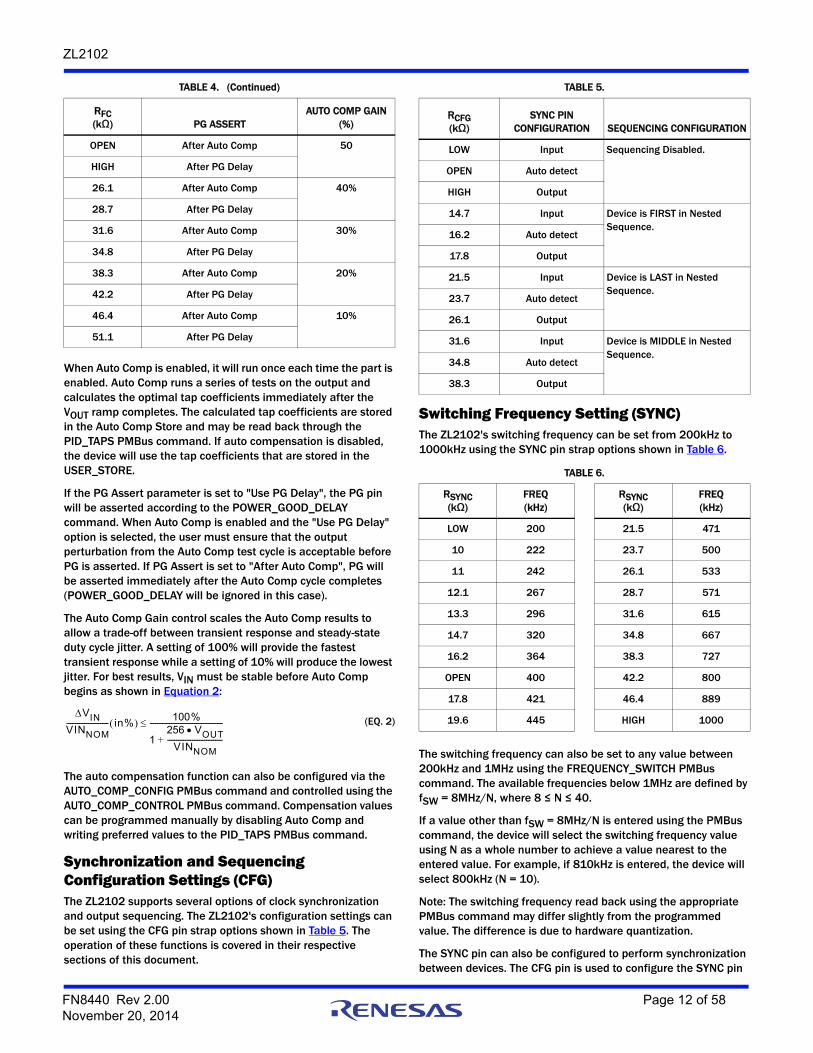
Typical Performance CurvesFor some applications, ZL2102 operating conditions (input voltage, output voltage, switching frequency, temperature) may require derating to remain within the Safe Operating Area (SOA). VIN = VDDP = VDDS, TJ = +125°C
FIGURE 3. LOW-SIDE rDS(ON) vs TJ NORMALIZED FOR TJ = +25°C (VDDS = 12V, IDRAIN = 0.3A)
FIGURE 4. HIGH-SIDE rDS(ON) vs TJ NORMALIZED FOR TJ = +25°C (VDDS = 12V, BST – SW = 6.5V, IDRAIN = 0.3A)
0.8
0.9
1.0
1.1
1.2
1.3
1.4
0 25 50 75 100
TJ (°C)
NO
RM
AL
IZE
D r
DS
(ON
)
0.8
0.9
1.0
1.1
1.2
1.3
1.4
0 25 50 75 100
TJ (°C)
NO
RM
AL
IZE
D r
DS
(ON
)
FN8440 Rev 2.00 Page 7 of 58November 20, 2014

ZL2102
Digital-DC Architecture OverviewThe ZL2102 is an innovative mixed-signal power conversion and power management IC based on Intersil patented Digital-DC technology that provides an integrated, high performance stepdown regulator for point of load applications. The ZL2102 integrates all necessary PWM control circuitry as well as low rDS(ON) synchronous power MOSFETs to provide an extremely small solution for supplying load currents up to 6A.
Its unique PWM loop utilizes an ideal mix of analog and digital blocks to enable precise control of the entire power conversion process with no software required, resulting in a very flexible device that is also very easy to use. An extensive set of power management functions are fully integrated and can be configured using simple pin connections. The user configuration can be saved in an internal nonvolatile memory (NVM). Additionally, all functions can be configured and monitored via the SMBus hardware interface using standard PMBus commands, allowing ultimate flexibility.
Once enabled, the ZL2102 is immediately ready to regulate power and perform power management tasks with no programming required. Advanced configuration options and realtime configuration changes are available via the SMBus interface if desired and continuous monitoring of multiple operating parameters is possible with minimal interaction from a host controller. Integrated sub regulation circuitry enables single supply operation from any external supply between 4.5V and 14V with no additional bias supplies needed.
The ZL2102 can be configured by simply connecting its pins according to the tables provided in the following sections. Additionally, a comprehensive set of application notes are available to help simplify the design process. An evaluation board is also available to help the user become familiar with the device. This board can be evaluated as a standalone platform using pin configuration settings. A Windows™-based GUI is also provided to enable full configuration and monitoring capability via the SMBus interface using a computer and the included USB cable.
FIGURE 5. LOW-SIDE rDS(ON) vs VDDS WITH TJ FIGURE 6. SAFE OPERATING AREA, TJ +125°C
FIGURE 7. MAXIMUM CONVERSION RATIO, TJ +125°C
Typical Performance CurvesFor some applications, ZL2102 operating conditions (input voltage, output voltage, switching frequency, temperature) may require derating to remain within the Safe Operating Area (SOA). VIN = VDDP = VDDS, TJ = +125°C (Continued)
40
45
50
55
60
65
70
6 7 8 9 10 11 12 13
VDDS (V)
r DS
(ON
) (mΩ
) TJ = +110°C
TJ = +80°C
TJ = +50°C
TJ = +25°C
0
1
2
3
4
5
6
0.2 0.3 0.4 0.5 0.6 0.7 0.8 0.9 10
1
2
4
5
0.2 0.3 0.4 0.5 0.6 0.7 0.8 0.9 1.0
fSW (MHz)
VO
UT (
V)
VIN = 6V
VIN = 8.6V TO 14V
VIN = 7.5V
0.60
0.65
0.70
0.75
0.80
0.85
0.90
0.95
0.2 0.3 0.4 0.5 0.6 0.7 0.8 0.9 1.0
fSW (MHz)
VO
UT/V
IN (
V)
VOUT MAY NOT EXCEED
5.5V AT ANY TIME
FN8440 Rev 2.00 Page 8 of 58November 20, 2014

ZL2102
Power Conversion OverviewThe ZL2102 operates as a voltage-mode, synchronous buck converter with a selectable constant frequency pulse width modulator (PWM) control scheme. The ZL2102 integrates dual low rDS(ON) synchronous MOSFETs and a high-side driver to minimize the circuit footprint. Figure 8 illustrates the basic synchronous buck converter topology showing the primary power train components. This converter is also called a step-down converter, as the output voltage must always be lower than the input voltage.
The ZL2102 integrates two N-channel power MOSFETs; QH is the top control MOSFET and QL is the bottom synchronous MOSFET. The amount of time that QH is on as a fraction of the total switching period is known as duty cycle D, which is described by Equation 1:
During time D, QH is on and VIN to VOUT is applied across the inductor. The output current ramps up as shown in Figure 9.
When QH turns off (time 1-D), the current flowing in the inductor must continue to flow from the ground up through QL, during which the current ramps down. Since the output capacitor COUT exhibits low impedance at the switching frequency, the AC component of the inductor current is filtered from the output voltage so the load sees nearly a DC voltage.
The maximum conversion ratio is shown in Figure 7. Typically, buck converters specify a maximum duty cycle that effectively limits the maximum output voltage that can be realized for a given input voltage and switching frequency. This duty cycle limit ensures that the low-side MOSFET is allowed to turn on for a minimum amount of time during each switching cycle, which enables the bootstrap capacitor to be charged up and provide adequate gate drive voltage for the high-side MOSFET.
The block diagram for the ZL2102 is illustrated in Figure 2. In this circuit, the target output voltage is regulated by connecting the VSEN pin directly to the output regulation point. The VSEN signal is then compared to an internal reference voltage that had been set to the desired output voltage level by the user. The error signal derived from this comparison is converted to a digital value with an analog-to-digital (A/D) converter. The digital signal is also applied to an adjustable digital compensation filter and the compensated signal is used to derive the appropriate PWM duty cycle for driving the internal MOSFETs in a way that produces the desired output.
Power Management OverviewThe ZL2102 incorporates a wide range of configurable power management features that are simple to implement with no external components. Additionally, the ZL2102 includes circuit protection features that continuously safeguard the device and load from damage due to unexpected system faults. The ZL2102 can continuously monitor input voltage, output voltage/current, and internal temperature. A power-good output signal is also included to enable power-on reset functionality for an external processor.
All power management functions can be configured using either pin configuration techniques described in this document or via the SMBus interface using PMBus commands. Monitoring parameters can also be preconfigured to provide alerts for specific conditions. “PMBus Command Summary” on page 19 contains a listing of all the PMBus commands supported by the ZL2102 and a detailed description of the use of each of these commands.
Functional Description and Configuration
INTERNAL BIAS REGULATORS AND INPUT SUPPLY CONNECTIONSThe ZL2102 employs three internal LDO regulators, allowing operation from a single input supply from 4.5V to 14V. The regulators are as follows:
• VR is derived from VDDS and provides a 7V bias supply for the internal high-side MOSFET driver circuit. A 4.7µF capacitor is required for the VR pin.
• VRA is derived from VDDS and provides a 5V bias supply for the internal analog circuitry. A 4.7µF capacitor is required for the VR pin.
• V2P5 is derived from VRA and provides a 2.5V bias supply for the digital circuitry. A 10µF capacitor is required at the V2P5 pin.
VIN
VOUT
QH
QL
L1
COUT
ZL2102
CIN
CB
DB
PWM
LDO
FIGURE 8. STEP DOWN CONVERTER
DVOUTVIN---------------- (EQ. 1)
VO
LT
AG
E
(V)
TIME
CU
RR
EN
T (
A)
VIN - VOUT
0
-VOUT
1 - D
IO
ILPK
ILV
D
FIGURE 9. OUTPUT CURRENT
FN8440 Rev 2.00 Page 9 of 58November 20, 2014

ZL2102
Input voltage ranges and connections are shown in Figure 10.
The internal bias regulators, VR and VRA, are not designed to be outputs for powering other circuitry. Do not attach external loads to any of these pins. Only the multimode pins may be connected to the V2P5 pin for logic HIGH settings.
MULTIMODE PINSIn order to simplify circuit design, the ZL2102 incorporates patented multimode pins that allow the user to easily configure many aspects of the device with no programming. Most power management features can be configured using these pins. The multimode pins can respond to four different connections as shown in Table 1. These pins are sampled once when power is applied or by issuing a PMBus Restore command.
Pin Strap Settings: This is the simplest implementation method, as no external components are required. Using this method, each pin can take on one of three possible states: LOW, OPEN, or HIGH. These pins can be connected to the V25 pin for logic HIGH settings. Using a single pin, one of three settings can be selected.
Resistor Settings: This method allows a greater range of adjustability when connecting a finite value resistor (in a specified range) between the multimode pin and SGND. Standard 1% resistor values are used, and only every fourth E96 resistor value is used so the device can reliably recognize the value of resistance connected to the pin while eliminating the error associated with the resistor accuracy. Up to 31 unique selections are available using a single resistor.
SMBus: Most ZL2102 functions/parameters can be configured via the SMBus interface using standard PMBus commands. “PMBus Command Summary” on page 19 explains the use of the available PMBus commands in detail.
CONFIGURABLE PINSMany operating parameters can be set using the multimode pin setup method: SMBus address (SA), output voltage (VSET), clock synchronization and sequencing options (CFG), switching frequency (SYNC), soft-start delay, soft-start ramp, input undervoltage lock-out (SS), and automatic loop compensation settings (FC). These pins are checked once during start-up only. Changes to the settings of these pins will not be read until the device's power supply has been cycled off and on.
The device's SMBus address is the only parameter that must be set by the multimode pins. All others are configurable using PMBus commands.
SMBus Device Address Selection (SA)The ZL2102 provides an SMBus digital interface that enables the user to configure all aspects of the device operation as well as monitor the input and output parameters. The ZL2102 is compatible with SMBus version 2.0 and includes an SALRT line to help mitigate bandwidth limitations related to continuous fault monitoring.
When communicating with multiple devices using the SMBus interface, each device must have its own unique address so the host can distinguish between the devices. The device address can be set according to the pin strap options listed in Table 2. The SMBus address cannot be changed with a PMBus command.
TABLE 1. MULTIMODE PIN CONFIGURATION
PIN TIED TO VALUE
LOW (Logic LOW) <0.8 VDC
OPEN (N/C) No connection
HIGH (Logic HIGH) >2.0 VDC
Resistor to SGND Set by resistor value
FIGURE 10. INPUT SUPPLY CONNECTIONS
VIN = 7.5V TO 14V
VIN = 4.5V TO 5.5V
VIN = 5.5V TO 7.5V
VR
VRA
VDDS
VIN
VDDS
VR
VRA
VIN
VDDS
VR
VRA
VIN
FIGURE 11. PIN STRAP AND RESISTOR SETTING EXAMPLES
MULTIMODE PIN
PIN STRAP SETTINGS
RESISTOR SETTINGS
MULTIMODE PIN
LOGIC HIGH
OPEN
LOGIC LOW
FN8440 Rev 2.00 Page 10 of 58November 20, 2014

ZL2102
Output Voltage and VOUT_MAX Selection (VSET)The output voltage may be set to any voltage between 0.6V and 5.5V provided that the input voltage is higher than the desired output voltage by an amount sufficient to prevent the device from exceeding its maximum duty cycle specification. VOUT can be set to any of the pin strap options shown in Table 3. VOUT can also be set using the VOUT_COMMAND PMBus command.
The maximum accepted value of VOUT is limited by VOUT_MAX. The default value of VOUT_MAX is 110% of the VSET pin strap setting, but it can also be set using the VOUT_MAX PMBus command.
In addition to the VOUT_COMMAND and VOUT_MAX settings, this pin strap setting is also used to set several other VOUT related settings including:
• VOUT_UV_FAULT_LIMIT = 85% of VSET
• POWER_GOOD_ON = 90% of VSET
• VOUT_MARGIN_LOW = 95% of VSET
• VOUT_MARGIN_HIGH = 105% of VSET
• VOUT_OV_FAULT_LIMIT = 115% of VSET
The above parameters are automatically adjusted by the VSET pin strap selection. If the value of VOUT_COMMAND is adjusted via PMBus, the values of these commands may also need to be adjusted to compensate for the VOUT change. The configured voltage relationships must follow: VOUT_UV_FAULT_LIMIT < POWER_GOOD_ON < VOUT_MARGIN_LOW < VOUT_COMMAND < VOUT_MARGIN_HIGH < VOUT_OV_FAULT_LIMIT.
Automatic Loop Compensation (FC)The ZL2102 has an automatic loop compensation feature that measures the characteristics of the power train and calculates the proper PID tap coefficients. Auto compensation is configured using the FC pin as shown in Table 4.
TABLE 2. PIN STRAP OPTIONS
RSA (kΩ)
SMBus ADDRESS
RSA (kΩ)
SMBus ADDRESS
10 or LOW 20h 42.2 2Fh
11 or OPEN 21h 46.4 30h
12.1 or HIGH 22h 51.1 31h
13.3 23h 56.2 32h
14.7 24h 61.9 33h
16.2 25h 68.1 34h
17.8 26h 75 35h
19.6 27h 82.5 36h
21.5 28h 91 37h
23.7 29h 100 38h
26.1 2Ah 110 39h
28.7 2Bh 121 3Ah
31.6 2Ch 133 3Bh
34.8 2Dh 147 3Ch
38.3 2Eh 162 3Dh
TABLE 3.
RSET(kΩ)
VOUT (V)
RSET (kΩ)
VOUT (V)
10 0.6 LOW 1.8
11 0.7 51.1 1.9
12.1 0.75 56.2 2
13.3 0.8 61.9 2.1
14.7 0.9 68.1 2.2
16.2 1 75 2.4
17.8 1.05 82.5 2.5
19.6 1.1 91 2.6
21.5 1.125 100 2.7
23.7 1.15 110 2.8
26.1 1.2 121 2.9
28.7 1.25 133 3
31.6 1.3 HIGH 3.3
34.8 1.4 147 4
38.3 1.5 162 4.5
42.2 1.6 OPEN 5
46.4 1.7
TABLE 4.
RFC (kΩ) PG ASSERT
AUTO COMP GAIN(%)
LOW Auto Comp Disabled
10 After Auto Comp 100
11 After PG Delay
12.1 After Auto Comp 90
13.3 After PG Delay
14.7 After Auto Comp 80
16.2 After PG Delay
17.8 After Auto Comp 70
19.6 After PG Delay
21.5 After Auto Comp 60
23.7 After PG Delay
TABLE 3. (Continued)
RSET(kΩ)
VOUT (V)
RSET (kΩ)
VOUT (V)
FN8440 Rev 2.00 Page 11 of 58November 20, 2014
ZL2102
When Auto Comp is enabled, it will run once each time the part is enabled. Auto Comp runs a series of tests on the output and calculates the optimal tap coefficients immediately after the VOUT ramp completes. The calculated tap coefficients are stored in the Auto Comp Store and may be read back through the PID_TAPS PMBus command. If auto compensation is disabled, the device will use the tap coefficients that are stored in the USER_STORE.
If the PG Assert parameter is set to "Use PG Delay", the PG pin will be asserted according to the POWER_GOOD_DELAY command. When Auto Comp is enabled and the "Use PG Delay" option is selected, the user must ensure that the output perturbation from the Auto Comp test cycle is acceptable before PG is asserted. If PG Assert is set to "After Auto Comp", PG will be asserted immediately after the Auto Comp cycle completes (POWER_GOOD_DELAY will be ignored in this case).
The Auto Comp Gain control scales the Auto Comp results to allow a trade-off between transient response and steady-state duty cycle jitter. A setting of 100% will provide the fastest transient response while a setting of 10% will produce the lowest jitter. For best results, VIN must be stable before Auto Comp begins as shown in Equation 2:
The auto compensation function can also be configured via the AUTO_COMP_CONFIG PMBus command and controlled using the AUTO_COMP_CONTROL PMBus command. Compensation values can be programmed manually by disabling Auto Comp and writing preferred values to the PID_TAPS PMBus command.
Synchronization and Sequencing Configuration Settings (CFG)The ZL2102 supports several options of clock synchronization and output sequencing. The ZL2102's configuration settings can be set using the CFG pin strap options shown in Table 5. The operation of these functions is covered in their respective sections of this document.
Switching Frequency Setting (SYNC)The ZL2102's switching frequency can be set from 200kHz to 1000kHz using the SYNC pin strap options shown in Table 6.
The switching frequency can also be set to any value between 200kHz and 1MHz using the FREQUENCY_SWITCH PMBus command. The available frequencies below 1MHz are defined by fSW = 8MHz/N, where 8 ≤ N ≤ 40.
If a value other than fSW = 8MHz/N is entered using the PMBus command, the device will select the switching frequency value using N as a whole number to achieve a value nearest to the entered value. For example, if 810kHz is entered, the device will select 800kHz (N = 10).
Note: The switching frequency read back using the appropriate PMBus command may differ slightly from the programmed value. The difference is due to hardware quantization.
The SYNC pin can also be configured to perform synchronization between devices. The CFG pin is used to configure the SYNC pin
OPEN After Auto Comp 50
HIGH After PG Delay
26.1 After Auto Comp 40%
28.7 After PG Delay
31.6 After Auto Comp 30%
34.8 After PG Delay
38.3 After Auto Comp 20%
42.2 After PG Delay
46.4 After Auto Comp 10%
51.1 After PG Delay
TABLE 4. (Continued)
RFC (kΩ) PG ASSERT
AUTO COMP GAIN(%)
VINVINNOM------------------------ in% 100%
1256 VOUT
VINNOM-------------------------------+
----------------------------------------- (EQ. 2)
TABLE 5.
RCFG(kΩ)
SYNC PIN CONFIGURATION SEQUENCING CONFIGURATION
LOW Input Sequencing Disabled.
OPEN Auto detect
HIGH Output
14.7 Input Device is FIRST in Nested Sequence.
16.2 Auto detect
17.8 Output
21.5 Input Device is LAST in Nested Sequence.
23.7 Auto detect
26.1 Output
31.6 Input Device is MIDDLE in Nested Sequence.
34.8 Auto detect
38.3 Output
TABLE 6.
RSYNC(kΩ)
FREQ (kHz)
RSYNC(kΩ)
FREQ(kHz)
LOW 200 21.5 471
10 222 23.7 500
11 242 26.1 533
12.1 267 28.7 571
13.3 296 31.6 615
14.7 320 34.8 667
16.2 364 38.3 727
OPEN 400 42.2 800
17.8 421 46.4 889
19.6 445 HIGH 1000
FN8440 Rev 2.00 Page 12 of 58November 20, 2014

ZL2102
as an input, an output, or auto-detect mode. The ZL2102 incorporates an internal phase-locked loop (PLL) to clock the internal circuitry. The PLL can be driven by an external clock source connected to the SYNC pin, or it can be configured to drive the internal clock out of the SYNC pin to other devices.
SYNC OUTPUT: When the SYNC pin is configured as an output, the device will run from its internal oscillator and will drive the selected switching frequency onto the SYNC pin so that other devices can be synchronized to it.
SYNC INPUT: When the SYNC pin is configured as an input, the device will check for an external clock signal on the SYNC pin each time the output is enabled. The internal oscillator will then synchronize with the rising edge of the external clock. The incoming clock signal must be in the range of 200kHz to 1MHz and must be stable when the enable pin is asserted. The clock signal must have a minimum width of 150ns, and it must stay within 10% of its initial value. In the event of a loss of the external clock signal, will automatically switch to its internal oscillator and switch at a frequency close to the previous incoming frequency. The output voltage may show a transient overshoot/undershoot if this occurs.
SYNC AUTO DETECT: When the SYNC pin is configured in auto-detect mode, the device will check for a clock signal on the SYNC pin each time EN is asserted. If there is a valid clock, the pin will run as a sync input.
If no incoming clock signal is present, the device will switch at the selected internal clock rate.
Soft-Start and UVLO Settings (SS)The ZL2102 supports variable turn-on/off delay times, turn-on/off ramp rates, and input undervoltage lockout (UVLO) functions. These features may be used as part of an overall in-rush current management strategy or to precisely control how fast a load is turned on. The ZL2102 provides several options for precisely and independently controlling both the delay and ramp time periods.
The soft-start delay period begins when the EN pin is asserted and ends when the delay time expires. The soft-start ramp timer enables a precisely controlled monotonic ramp to the nominal VOUT value that begins once the delay period has expired. This process is also followed for ramp down after the EN pin has been deasserted.
The input undervoltage lockout (UVLO) prevents the ZL2102 from operating when the input falls below a preset threshold, indicating the input supply is out of its specified range.
The ZL2102's TON/TOFF delay time, TON/TOFF ramp time, and UVLO functions can be configured using the SS pin strap options shown in Table 7.
These functions can also be set independently using TON_DELAY, TON_RISE, TOFF_DELAY, and TOFF_FALL PMBus commands. The UVLO threshold can be adjusted using the VIN_UV_FAULT_LIMIT PMBus command. The ramp down function is disabled by default, but it can be enabled using the ON_OFF_CONFIG or OPERATION PMBus commands depending on the desired device enable method.
Start-up ProcedureThe ZL2102 follows a specific internal start-up procedure after power is applied. Figure 12 describes the start-up sequence.
TABLE 7.
RSS(kΩ)
TON/TOFF DELAY TIME(ms)
TON/TOFFRAMP TIME
(ms)UVLO
(V)
10 5
5
4.5
11 10
12.1 20
LOW or 13.3 5
1014.7 10
16.2 20
17.8 5
2019.6 10
21.5 20
23.7 5
5
5.5
26.1 10
HIGH or 28.7 20
31.6 5
1034.8 10
38.3 20
42.2 5
2046.4 10
51.1 20
56.2 5
5
7.5
OPEN or 61.9 10
68.1 20
75 5
1082.5 10
91 20
100 5
20110 10
121 20
FN8440 Rev 2.00 Page 13 of 58November 20, 2014

ZL2102
If the device is to be synchronized to an external clock source, the clock frequency must be stable prior to asserting the EN pin. The device requires approximately 35ms to check for specific values stored in its internal memory. If the user has stored values in memory, those values will be loaded. If Auto Comp is enabled, start-up time increases to ~55ms.
Once this process is completed, the device is ready to accept commands via the serial interface and the device is ready to be enabled. Once enabled, the device requires approximately 5ms before its output voltage may be allowed to start its ramp-up process. If a soft-start delay period less than 5ms has been configured (using PMBus commands), the device will default to a 5ms delay period. If a delay period greater than 5ms is configured, the device will wait for the configured delay period prior to starting to ramp its output.
After the delay period has expired, the output will begin to ramp towards its target voltage according to the preconfigured soft-start ramp time.
Power-GoodThe ZL2102 provides a Power-Good (PG) signal that indicates the output voltage is within a specified tolerance of its target level and no fault condition exists. By default, the PG pin will assert if the output reaches 90% of the target voltage. The limit and drive configuration of the pin may be changed using the POWER_GOOD_ON and MFR_CONFIG PMBus commands.
A PG delay period is defined as the time from when all conditions for asserting PG are met to when the PG pin is actually asserted. This feature is commonly used instead of using an external reset controller to control external digital logic. By default, the ZL2102 PG delay is set equal to 1ms. The PG delay can be adjusted using the POWER_GOOD_DELAY PMBus command.
Power Management Function DescriptionInput Undervoltage LockoutThe input undervoltage lockout feature (UVLO) prevents the ZL2102 from operating when the input falls below a preset threshold, indicating the input supply is out of its specified range. The UVLO threshold can be set to 4.5V, 5.5V, or 7.5V using the SS pin. The UVLO voltage can also be adjusted using the VIN_UV_FAULT_LIMIT PMBus command.
The default response from a UVLO fault is an immediate shutdown of the device during the fault and an automatic restart when the fault condition has cleared. The UVLO fault response can be configured using the VIN_UV_FAULT_RESPONSE PMBus command.
Output Overvoltage ProtectionThe ZL2102 offers an internal output overvoltage protection circuit that can be used to protect sensitive load circuitry from being subjected to a voltage higher than its prescribed limits. A hardware comparator is used to compare the actual output voltage (seen at the VSEN pin) to a threshold set above the target output voltage. The default setting is 115% of the pin strap setting for VOUT, but this value can be adjusted using the VOUT_OV_FAULT_LIMIT PMBus command. If the VSEN voltage exceeds this threshold, the PG pin will deassert and the device response can be set using the VOUT_OV_FAULT_RESPONSE PMBus command. The default response is an immediate shutdown of the device during the fault and an automatic restart when the fault has cleared. For continuous overvoltage protection when operating from an external clock, the only allowed response is an immediate shutdown with no automatic restart.
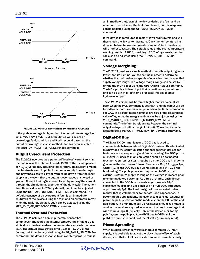
Output Prebias ProtectionAn output prebias condition exists when an externally applied voltage is present on a power supply's output before the power supply's control IC is enabled. Certain applications require that the converter not be allowed to sink current during start-up if a prebias condition exists at the output. The ZL2102 provides prebias protection by sampling the output voltage prior to initiating an output ramp.
If a prebias voltage exists after the preconfigured delay period has expired, the ramp start voltage will be set to match the existing prebias voltage and the output will be enabled. The output voltage will then ramp to the final regulation value at the ramp rate set by the SS pin strap setting or the TON_RISE PMBus command.
The actual time the output will take to ramp up from the prebias voltage to the target voltage will vary depending on the prebias voltage, but the total time from enable to when the output reaches its target value will match the preconfigured delay and ramp times. When ramping down from a prebias higher than the target voltage, the device will wait until after SS ramp time is complete and will then ramp down to the target voltage at an approximate rate of 0.1V/ms (see Figure 13).
Input Power Applied
Internal Memory Check~35ms
Device will ignore an enable signal or PMBus
commands
Device Ready
Pre-ramp Delay~5ms
Delay between enable signal and start of output ramp. Additional delay may be
added with PMBus command
FIGURE 12. START-UP SEQUENCE
FN8440 Rev 2.00 Page 14 of 58November 20, 2014
ZL2102
If the prebias voltage is higher than the output overvoltage limit set in VOUT_OV_FAULT_LIMIT, the device will declare an overvoltage fault condition and it will respond based on the output overvoltage response method that has been selected in the VOUT_OV_FAULT_RESPONSE PMBus command.
Output Overcurrent ProtectionThe ZL2102 incorporates a patented "lossless" current sensing method across the internal low-side MOSFET that is independent of rDS(ON) variations, including temperature. This current limiting mechanism is used to protect the power supply from damage and prevent excessive current from being drawn from the input supply in the event that the output is overloaded or shorted to ground. Current limiting is accomplished by sensing the current through the circuit during a portion of the duty cycle. The current limit threshold is set to 7.2A by default, but it can be adjusted using the IOUT_AVG_OC_FAULT_LIMIT PMBus command. The default response of an overcurrent fault is an immediate shutdown of the device during the fault and an automatic restart when the fault has cleared, but it can be adjusted using the MFR_IOUT_OC_RESPONSE PMBus command.
Thermal Overload ProtectionThe ZL2102 includes an on-chip thermal sensor that continuously measures the internal temperature of the die and shuts down the device when the temperature exceeds the preset limit. The default temperature limit is set to +125°C in the factory, but it can be adjusted using the OT_FAULT_LIMIT PMBus command. The default response to an over-temperature fault is
an immediate shutdown of the device during the fault and an automatic restart when the fault has cleared, but the response can be adjusted using the OT_FAULT_RESPONSE PMBus command.
If the device is configured to restart, it will wait 250ms and will then check the device temperature. Once the temperature has dropped below the over-temperature warning limit, the device will attempt to restart. The default value of the over-temperature warning limit is +110°C, providing +15°C of hysteresis, but the value can be adjusted using the OT_WARN_LIMIT PMBus command.
Voltage MarginingThe ZL2102 provides a simple method to vary its output higher or lower than its nominal voltage setting in order to determine whether the load device is capable of operating over its specified supply voltage range. The voltage margin range can be set by driving the MGN pin or using the OPERATION PMBus command. The MGN pin is a tri-level input that is continuously monitored and can be driven directly by a processor I/O pin or other logic-level output.
The ZL2102's output will be forced higher than its nominal set point when the MGN command is set HIGH, and the output will be forced lower than its nominal set point when the MGN command is set LOW. The default margin settings are ±5% of the pin strapped value of VOUT, but the margin settings can be adjusted using the VOUT_MARGIN_HIGH and VOUT_MARGIN_LOW PMBus commands. The default transition rate between the nominal output voltage and either margin limit is 0.5V/ms, but it can be adjusted using the VOUT_TRANSITION_RATE PMBus command.
Digital-DC BusThe Digital-DC Communications (DDC) bus is used to communicate between Intersil Digital-DC devices. This dedicated bus provides the communication channel between devices for features such as sequencing and fault spreading. The DDC pin on all Digital-DC devices in an application should be connected together. A pull-up resistor is required on the DDC bus in order to guarantee the rise time as follows: Rise time = RPU * CLOAD ≈ 1µs, where RPU is the DDC bus pull-up resistance and CLOAD is the bus loading. The pull-up resistor may be tied to VR or to an external 3.3V or 5V supply as long as this voltage is present prior to or during device power-up. As a rule of thumb, each device connected to the DDC bus presents approximately 10pF of capacitive loading, and each inch of FR4 PCB trace introduces approximately 2pF. The ideal design will use a central pull-up resistor that is well-matched to the total load capacitance. In power module applications, the user should consider whether to place the pull-up resistor on the module or on the PCB of the end application. The minimum pull-up resistance should be limited to a value that enables any device to assert the bus to a voltage that will ensure a logic 0 (typically 0.8V at the device monitoring point) given the pull-up voltage (5V if tied to VR5) and the pull-down current capability of the ZL2102 (nominally 4mA).
Phase SpreadingWhen multiple power converters share a common DC input supply, it is desirable to adjust the clock phase offset of each device, such that not all devices start to switch simultaneously.
FIGURE 13. OUTPUT RESPONSES TO PREBIAS VOLTAGES
SS DELAY
SSRAMP
TARGET VOLTAGE
PREBIAS VOLTAGE
VOUT
TIME
SS DELAY
SSRAMP
TARGET VOLTAGE
PREBIAS VOLTAGE
VOUT
TIME
VPREBIAS < VTARGET
VPREBIAS > VTARGET
FN8440 Rev 2.00 Page 15 of 58November 20, 2014

ZL2102
Setting each converter to start its switching cycle at a different point in time can dramatically reduce input capacitance requirements and efficiency losses. Since the peak current drawn from the input supply is effectively spread out over a period of time, the peak current drawn at any given moment is reduced and the power losses proportional to the IRMS
2 are reduced dramatically.
In order to enable phase spreading, all converters must be synchronized to the same switching clock. This can be accomplished by setting the CFG pin strap or by using the INTERLEAVE PMBus command.
Selecting the phase offset for the device is accomplished by selecting a device address according to Equation 3:
For example:
• A device address of 0x20 would configure no phase offset
• A device address of 0x21 would configure 45° of phase offset
• A device address of 0x22 would configure 90° of phase offset
The phase offset of each device may also be set to any value between 0° and 360° in 22.5° increments via the INTERLEAVE PMBus command.
Output SequencingIntersil devices may be configured to power-up as a group in a predetermined sequence. This feature is especially useful when powering advanced processors, FPGA’s and ASIC’s that require one supply to reach its operating voltage prior to another supply reaching its operating voltage in order to avoid latch-up from occurring. Multidevice sequencing can be achieved by configuring each device through the SEQUENCE PMBus command or by using Intersil patented autonomous sequencing mode.
Autonomous sequencing mode configures sequencing by using events transmitted between devices over the DDC bus. The sequencing order is determined using each device's SMBus address. Using autonomous sequencing mode (configured using the CFG pin), the devices must be assigned sequential SMBus addresses with no missing addresses in the chain, the enable pins must be tied together, and the sync pins of all devices must be tied together. The first device in the sequence will become the clock master, and the other devices will sync to this clock. This mode will also constrain each device to have a phase offset according to its SMBus address as described in the “Phase Spreading” on page 15.
The enable (EN) line is driven high to initiate a sequenced turn-on of the group. Enable is driven low to initiate a sequenced turnoff of the group. During enable, the sequencing group will enable in order starting with the device with the lowest SMBus address and will continue through to turn on each device in the address chain until all devices connected have been turned on. During disable, the device with the highest SMBus address will turn off first followed in reverse order by the other devices in the group. The PG threshold is used to determine when the following device is enabled.
Fault SpreadingDigital-DC devices can be configured to broadcast a fault event over the DDC bus to the other devices in the group. When a fault occurs and the device is configured to shut down on a fault, the device will shut down and broadcast the fault event over the DDC bus. The other devices on the DDC bus can be configured to respond to the broadcast in several ways including group shutdown/restart. Fault spreading mode can be enabled through the USER_CONFIG PMBus command, and the fault spreading group can be defined through the DDC_GROUP PMBus command.
Monitoring via SMBusA system controller can monitor a wide variety of different ZL2102 parameters through the SMBus interface. The device can monitor for fault conditions by monitoring the SALRT pin, which will be asserted when any number of preconfigured fault conditions occur.
The device can also be monitored continuously for many power conversion parameters including input voltage, output voltage, output current, internal junction temperature, switching frequency, duty cycle, fault status information.
The PMBus Host should respond to SALRT as follows:
• ZL device pulls SALRT Low.
• PMBus Host detects that SALRT is now low, performs transmission with Alert Response Address to find which ZL device is pulling SALRT low.
• PMBus Host talks to the ZL device that has pulled SALRT low. The actions that the host performs are up to the System Designer.
If multiple devices are faulting, SALRT will still be low after doing the above steps and will require transmission with the Alert Response Address repeatedly until all faults are cleared.
Nonvolatile MemoryThe ZL2102 has internal nonvolatile memory where user settings are stored. There are two storage locations; the factory store and the user store. During the initialization process, the ZL2102 checks for any stored values in the user store. If user programmed settings are found, they will be used for those parameters. If there are no user settings stored, the factory settings and pin strap values are used for those parameters.
Snapshot™ Parametric CaptureThe ZL2102 offers a special feature that enables the user to capture parametric data during normal operation or following a fault. The Snapshot function can be enabled through the MISC_CONFIG PMBus command, and the data can be read back as a block read transfer using the SNAPSHOT PMBus command.
The SNAPSHOT_CONTROL PMBus command enables the user to store the snapshot parameters to NV memory in response to a fault as well as to read the stored data from NV memory after a fault has occurred.
Automatic writes to NV memory following a fault are triggered when any fault threshold level is exceeded, provided that the
Phase offset device address 45= (EQ. 3)
FN8440 Rev 2.00 Page 16 of 58November 20, 2014

ZL2102
specific fault's response is to shut down. Writing to NV memory is not allowed if the device is configured to retry following the specific fault condition.
The device's VDD voltage must remain valid during the time when the device is writing the data to NV memory; a process that requires up to 2ms.
Power Train Component SelectionThe ZL2102 is a synchronous buck converter with MOSFETs that uses an external inductor and capacitors to perform the power conversion process. The proper selection of the external components is critical for optimized performance.
To select the appropriate external components for the desired performance goals, the power supply requirements listed in Table 8 must be known.
Design Goal Trade-offsThe design of the buck power stage requires several compromises among size, efficiency, and cost. The inductor core loss increases with frequency, so there is a trade-off between a small output filter made possible by a higher switching frequency and getting better power supply efficiency. Size can be decreased by increasing the switching frequency at the expense of efficiency. Cost can be minimized by using through-hole inductors and capacitors; however these components are physically large.
To start the design, select a switching frequency based on Table 9. This frequency is a starting point and may be adjusted as the design progresses.
Inductor SelectionThe output inductor selection process must include several trade-offs. A high inductance value will result in a low ripple current (Iopp), which will reduce output capacitance and produce a low output ripple voltage, but may also compromise output transient load performance. Therefore, a balance must be struck between output ripple and optimal load transient performance. A good starting point is to select the output inductor ripple equal to the expected load transient step magnitude (Iostep): Iopp = Iostep.
Now the output inductance can be calculated using Equation 4, where VINM is the maximum input voltage:
The average inductor current is equal to the maximum output current. The peak inductor current (ILpk) is calculated using Equation 5, where IOUT is the maximum output current:
Select an inductor rated for the average DC current with a peak current rating above the peak current computed in Equation 5.
In overcurrent or short-circuit conditions, the inductor may have currents greater than 2x the normal maximum rated output current. It is desirable to use an inductor that still provides some inductance at maximum current to protect the load and the internal MOSFETs from damaging currents in this situation.
Once an inductor is selected, the DCR and core losses in the inductor are calculated. Use the DCR specified in the inductor manufacturer's datasheet.
ILrms is given by:
where IOUT is the maximum output current. Next, calculate the core loss of the selected inductor. Since this calculation is specific to each inductor and manufacturer, refer to the chosen inductor datasheet. Add the core loss and the ESR loss and compare the total loss to the maximum power dissipation recommendation in the inductor datasheet.
Output Capacitor SelectionSeveral trade-offs must also be considered when selecting an output capacitor. Low ESR values are needed to have a small output deviation during transient load steps (Vosag) and low output voltage ripple (Vorip). However, capacitors with low ESR, such as semi-stable (X5R and X7R) dielectric ceramic capacitors, also have relatively low capacitance values. Many designs can use a combination of high capacitance devices and low ESR devices in parallel.
For high ripple currents, a low capacitance value can cause a significant amount of output voltage ripple. Likewise, in high transient load steps, a relatively large amount of capacitance is
TABLE 8. TABLE SUPPLY REQUIREMENTS
PARAMETER RANGE EXAMPLE VALUE
Input voltage (VIN) 4.5V to 14.0V 12V
Output voltage (VOUT) 0.6V to 5.0V 3.3V
Output current (IOUT) 0A to 6A 4A
Output voltage ripple(Vorip)
<3% of VOUT 1% of VOUT
Output load step (Iostep) <Io ±25% of Io
Output load step rate - 2.5A/µs
Output deviation due to load step - ±3% of VOUT
Maximum PCB temp. +120°C +85°C
Desired efficiency - 85%
Other considerations - Optimize for small size
TABLE 9. CIRCUIT DESIGN CONSIDERATION
FREQUENCY RANGE EFFICIENCY CIRCUIT SIZE
200kHz to 400kHz Highest Larger
400kHz to 800kHz Moderate Smaller
800kHz to 1MHz Lower Smallest
LOUT
VOUT 1VOUTVINM----------------–
fSW Iopp-----------------------------------------------------= (EQ. 4)
ILpk IOUT
Iopp2
-----------+= (EQ. 5)
PLDCR DCR ILrms2= (EQ. 6)
ILrms IOUT2Iopp 2
12--------------------+=
(EQ. 7)
FN8440 Rev 2.00 Page 17 of 58November 20, 2014

ZL2102
needed to minimize the output voltage deviation while the inductor current ramps up or down to the new steady state output current value.
As a starting point, apportion one-half of the output ripple voltage to the capacitor ESR and the other half to capacitance, as shown in the following equations:
Use these values to make an initial capacitor selection, using a single capacitor or several capacitors in parallel.
After a capacitor has been selected, the resulting output voltage ripple can be calculated using Equation 10:
Because each part of this equation was made to be less than or equal to half of the allowed output ripple voltage, the Vorip should be less than the desired maximum output ripple.
Input CapacitorIt is highly recommended that dedicated input capacitors be used in any point of load design, even when the supply is powered from a heavily filtered 5V or 12V "bulk" supply from an off-line power supply. This is because of the high RMS ripple current that is drawn by the buck converter topology. This ripple (ICINrms) can be determined from Equation 11:
Without capacitive filtering near the power supply circuit, this current would flow through the supply bus and return planes, coupling noise into other system circuitry. The input capacitors should be rated at 1.2x the ripple current calculated above to avoid overheating of the capacitors due to the high ripple current, which can cause premature failure. Ceramic capacitors with X7R or X5R dielectric with low ESR and 1.1x the maximum expected input voltage are recommended.
BOOTSTRAP CAPACITOR SELECTIONThe high-side driver boost circuit utilizes an internal Schottky diode (DB) and an external bootstrap capacitor (CB) to supply sufficient gate drive for the high-side MOSFET driver. CB should be a 0.1µF ceramic type rated for at least 10V.
CV2P5 SELECTIONThis capacitor is used to both stabilize and provide noise filtering for the 2.5V internal power supply. It should be between 4.7µF and 10µF, should use a semi-stable X5R or X7R dielectric ceramic with a low ESR (less than 10mΩ) and should have a rating of 4V or more.
CVR SELECTIONThis capacitor is used to both stabilize and provide noise filtering for the 7V reference supply. It should be 4.7µF, should use a
semi-stable X5R or X7R dielectric ceramic capacitor with a low ESR (less than 10mΩ) and should have a rating of 10V or more.
CVRA SELECTIONThis capacitor is used to both stabilize and provide noise filtering for the analog 5V reference supply. It should be 4.7µF, should use a semi-stable X5R or X7R dielectric ceramic capacitor with a low ESR (less than 10mΩ) and should have a rating of 6.3V or more.
THERMAL CONSIDERATIONSIn typical applications, the ZL2102's high efficiency will limit the internal power dissipation inside the package. However, in applications that require a high ambient operating temperature the user must perform some thermal analysis to ensure that the ZL2102's maximum junction temperature is not exceeded.
The ZL2102 has a maximum junction temperature limit of +125°C, and the internal over-temperature limiting circuitry will force the device to shut down if its junction temperature exceeds this threshold. In order to calculate the maximum junction temperature, the user must first calculate the power dissipated inside the IC (PQ) as expressed in Equation 12:
The operating junction temperature can then be calculated using Equation 13:
Where Tpcb is the printed circuit board temperature (under the package) and JC is the junction-to-case thermal resistance for the ZL2102 package.
PCB Layout RecommendationThe PCB layout is a very important step to make sure the designed converter works well. For ZL2102, the power system is composed of the input capacitor, VDDP pins, output inductor, SWITCH pins, output capacitor, and the PGND pins. It is necessary to group these connections as closely as possible and the connecting traces among them should be direct, short and wide. The switching node of the ZL2102 should connect directly to the inductor with minimal distance. The ZL2102 PGND pins, input and output capacitors should be connected as closely as possible to each other on the power GND plane. The input capacitor should be tightly coupled to the VIN pin. The VSEN voltage feedback trace should be routed to avoid the switch node, and should be connected directly to the pad of the output capacitor. The thermal pad is connected to SGND, and PGND must be isolated from SGND aside from a single connection point at the SGND pin.
The heat of the IC is mainly dissipated through the thermal pad. It is recommended to pass the heat from the thermal pad through the PCB using a large number of thermal vias. Connect as much copper as possible to these thermal vias throughout the PCB layers to help dissipate the heat, but do not route this SGND connection underneath any of the power components. The bottom layer is the best conductor of heat, so it should have at least 25mm2 of copper connected to these vias. Any traces that must be routed in this copper area should be radial in nature so
COUT
Iopp
8 fSW
Vorip2
--------------
-----------------------------------------= (EQ. 8)
ESRVorip
2 Iopp---------------------= (EQ. 9)
Vorip Iopp ESRIopp
8 fSW COUT-------------------------------------------+= (EQ. 10)
ICINrms IOUT D 1 D– = (EQ. 11)
PQ ILOAD2 rDS ON QH D rDS ON QL 1 D– + = (EQ. 12)
Ti Tpcb PQ JC+= (EQ. 13)
FN8440 Rev 2.00 Page 18 of 58November 20, 2014
ZL2102
that the thermal path from the thermal vias outward is not interrupted.
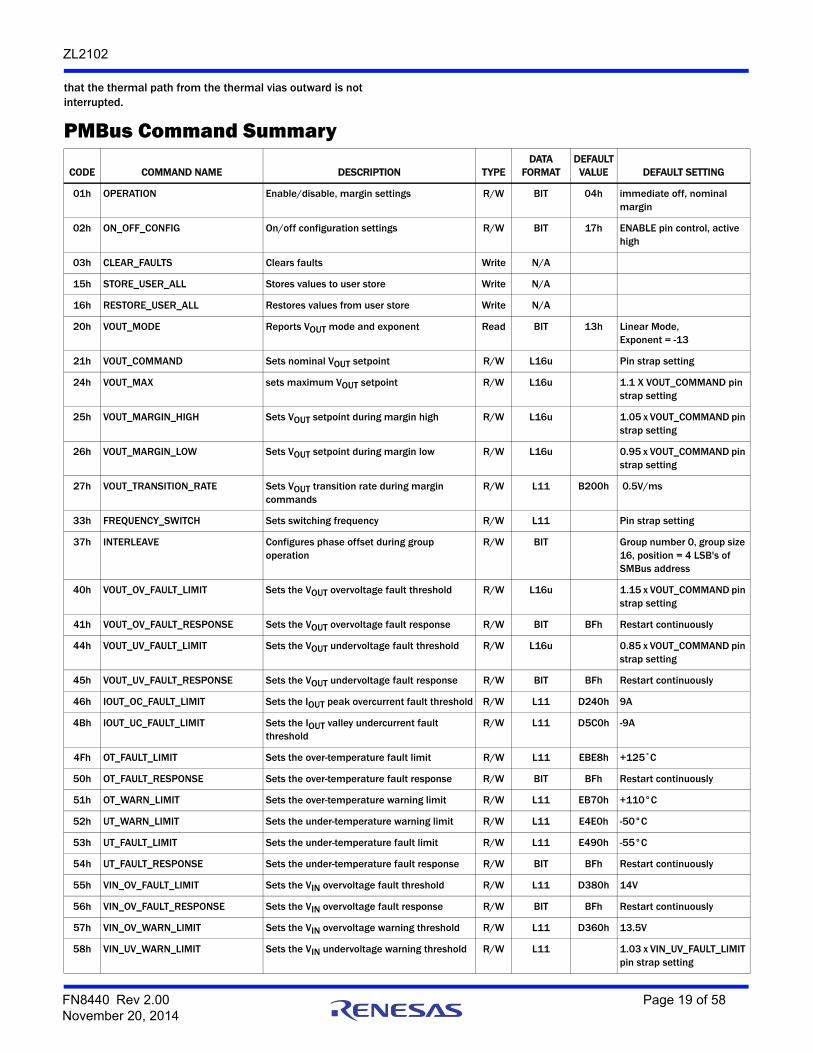
PMBus Command Summary
CODE COMMAND NAME DESCRIPTION TYPEDATA
FORMATDEFAULT
VALUE DEFAULT SETTING
01h OPERATION Enable/disable, margin settings R/W BIT 04h immediate off, nominal margin
02h ON_OFF_CONFIG On/off configuration settings R/W BIT 17h ENABLE pin control, active high
03h CLEAR_FAULTS Clears faults Write N/A
15h STORE_USER_ALL Stores values to user store Write N/A
16h RESTORE_USER_ALL Restores values from user store Write N/A
20h VOUT_MODE Reports VOUT mode and exponent Read BIT 13h Linear Mode, Exponent = -13
21h VOUT_COMMAND Sets nominal VOUT setpoint R/W L16u Pin strap setting
24h VOUT_MAX sets maximum VOUT setpoint R/W L16u 1.1 X VOUT_COMMAND pin strap setting
25h VOUT_MARGIN_HIGH Sets VOUT setpoint during margin high R/W L16u 1.05 x VOUT_COMMAND pin strap setting
26h VOUT_MARGIN_LOW Sets VOUT setpoint during margin low R/W L16u 0.95 x VOUT_COMMAND pin strap setting
27h VOUT_TRANSITION_RATE Sets VOUT transition rate during margin commands
R/W L11 B200h 0.5V/ms
33h FREQUENCY_SWITCH Sets switching frequency R/W L11 Pin strap setting
37h INTERLEAVE Configures phase offset during group operation
R/W BIT Group number 0, group size 16, position = 4 LSB's of SMBus address
40h VOUT_OV_FAULT_LIMIT Sets the VOUT overvoltage fault threshold R/W L16u 1.15 x VOUT_COMMAND pin strap setting
41h VOUT_OV_FAULT_RESPONSE Sets the VOUT overvoltage fault response R/W BIT BFh Restart continuously
44h VOUT_UV_FAULT_LIMIT Sets the VOUT undervoltage fault threshold R/W L16u 0.85 x VOUT_COMMAND pin strap setting
45h VOUT_UV_FAULT_RESPONSE Sets the VOUT undervoltage fault response R/W BIT BFh Restart continuously
46h IOUT_OC_FAULT_LIMIT Sets the IOUT peak overcurrent fault threshold R/W L11 D240h 9A
4Bh IOUT_UC_FAULT_LIMIT Sets the IOUT valley undercurrent fault threshold
R/W L11 D5C0h -9A
4Fh OT_FAULT_LIMIT Sets the over-temperature fault limit R/W L11 EBE8h +125˚C
50h OT_FAULT_RESPONSE Sets the over-temperature fault response R/W BIT BFh Restart continuously
51h OT_WARN_LIMIT Sets the over-temperature warning limit R/W L11 EB70h +110°C
52h UT_WARN_LIMIT Sets the under-temperature warning limit R/W L11 E4E0h -50°C
53h UT_FAULT_LIMIT Sets the under-temperature fault limit R/W L11 E490h -55°C
54h UT_FAULT_RESPONSE Sets the under-temperature fault response R/W BIT BFh Restart continuously
55h VIN_OV_FAULT_LIMIT Sets the VIN overvoltage fault threshold R/W L11 D380h 14V
56h VIN_OV_FAULT_RESPONSE Sets the VIN overvoltage fault response R/W BIT BFh Restart continuously
57h VIN_OV_WARN_LIMIT Sets the VIN overvoltage warning threshold R/W L11 D360h 13.5V
58h VIN_UV_WARN_LIMIT Sets the VIN undervoltage warning threshold R/W L11 1.03 x VIN_UV_FAULT_LIMIT pin strap setting
FN8440 Rev 2.00 Page 19 of 58November 20, 2014

ZL2102
59h VIN_UV_FAULT_LIMIT Sets the VIN undervoltage fault threshold R/W L11 Pin strap setting
5Ah VIN_UV_FAULT_RESPONSE Sets the VIN undervoltage fault response R/W BIT BFh Restart continuously
5Eh POWER_GOOD_ON Sets the voltage threshold for Power-Good indication
R/W L16u 0.9 x VOUT_COMMAND pin strap setting
60h TON_DELAY Sets the delay time from enable to VOUT rise R/W L11 Pin strap setting
61h TON_RISE Sets the rise time of VOUT after ENABLE and TON_DELAY
R/W L11 Pin strap setting
64h TOFF_DELAY Sets the delay time from DISABLE to start of VOUT fall
R/W L11 1 x TON_DELAY pin strap value
65h TOFF_FALL Sets the fall time for VOUT after DISABLE and TOFF_DELAY
R/W L11 1 x TON_RISE pin strap setting
79h STATUS_WORD Summary of critical faults Read BIT
7Ah STATUS_VOUT Reports VOUT warnings/faults Read BIT
7Bh STATUS_IOUT Reports IOUT warnings/faults Read BIT
7Ch STATUS_INPUT Reports input warnings/faults Read BIT
7Dh STATUS_TEMPERATURE Reports temperature warnings/faults Read BIT
7Eh STATUS_CML Reports Communication, memory, logic errors Read BIT
80h STATUS_MFR_SPECIFIC Reports voltage monitoring/clock synchronization faults
Read BIT
88h READ_VIN Reports input voltage measurement Read L11
8Bh READ_VOUT Reports output voltage measurement Read L16u
8Ch READ_IOUT Reports output current measurement Read L11
8Dh READ_TEMPERATURE_1 Reports internal temperature measurement Read L11
94h READ_DUTY_CYCLE Reports actual duty cycle Read L11
95h READ_FREQUENCY Reports actual switching frequency Read L11
98h PMBUS_REVISION Reports PMBus revision compliance Read BIT 01h Part 1 Revision 1.0, Part II Revision 1.1
99h MFR_ID Sets a user defined identification R/W ASC <null>
ADh IC_DEVICE_ID Reports device identification information Read CUS
AEh IC_DEVICE_REV Reports device revision information Read CUS
B0h USER_DATA_00 Sets a user defined data R/W ASC <null>
BCh AUTO_COMP_CONFIG Sets auto compensation configuration R/W BIT Pin strap setting
BDh AUTO_COMP_CONTROL Initiates auto compensation algorithm Write N/A
D0h MFR_CONFIG Configures several manufacturer-level features
R/W BIT 4801h
D1h USER_CONFIG Configures several user-level features R/W BIT Pin strap setting
D3h DDC_CONFIG Configures the DDC bus R/W BIT Broadcast group = 0, DDC ID = 5 LSBs of SMBus address
D4h POWER_GOOD_DELAY Sets the delay between PG threshold and PG assertion
R/W L11 BA00h 1ms
D5h PID_TAPS Configures the control loop compensator coefficients
R/W CUS Dependent upon autocomp settings
PMBus Command Summary (Continued)
CODE COMMAND NAME DESCRIPTION TYPEDATA
FORMATDEFAULT
VALUE DEFAULT SETTING
FN8440 Rev 2.00 Page 20 of 58November 20, 2014
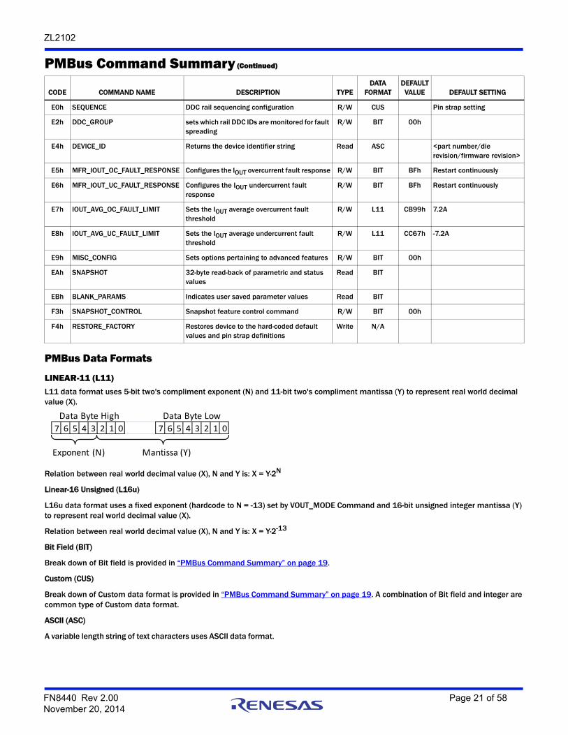
ZL2102
PMBus Data Formats
LINEAR-11 (L11) L11 data format uses 5-bit two's compliment exponent (N) and 11-bit two's compliment mantissa (Y) to represent real world decimal value (X).
Relation between real world decimal value (X), N and Y is: X = Y·2N
Linear-16 Unsigned (L16u)
L16u data format uses a fixed exponent (hardcode to N = -13) set by VOUT_MODE Command and 16-bit unsigned integer mantissa (Y) to represent real world decimal value (X).
Relation between real world decimal value (X), N and Y is: X = Y·2-13
Bit Field (BIT)
Break down of Bit field is provided in “PMBus Command Summary” on page 19.
Custom (CUS)
Break down of Custom data format is provided in “PMBus Command Summary” on page 19. A combination of Bit field and integer are common type of Custom data format.
ASCII (ASC)
A variable length string of text characters uses ASCII data format.
E0h SEQUENCE DDC rail sequencing configuration R/W CUS Pin strap setting
E2h DDC_GROUP sets which rail DDC IDs are monitored for fault spreading
R/W BIT 00h
E4h DEVICE_ID Returns the device identifier string Read ASC <part number/die revision/firmware revision>
E5h MFR_IOUT_OC_FAULT_RESPONSE Configures the IOUT overcurrent fault response R/W BIT BFh Restart continuously
E6h MFR_IOUT_UC_FAULT_RESPONSE Configures the IOUT undercurrent fault response
R/W BIT BFh Restart continuously
E7h IOUT_AVG_OC_FAULT_LIMIT Sets the IOUT average overcurrent fault threshold
R/W L11 CB99h 7.2A
E8h IOUT_AVG_UC_FAULT_LIMIT Sets the IOUT average undercurrent fault threshold
R/W L11 CC67h -7.2A
E9h MISC_CONFIG Sets options pertaining to advanced features R/W BIT 00h
EAh SNAPSHOT 32-byte read-back of parametric and status values
Read BIT
EBh BLANK_PARAMS Indicates user saved parameter values Read BIT
F3h SNAPSHOT_CONTROL Snapshot feature control command R/W BIT 00h
F4h RESTORE_FACTORY Restores device to the hard-coded default values and pin strap definitions
Write N/A
PMBus Command Summary (Continued)
CODE COMMAND NAME DESCRIPTION TYPEDATA
FORMATDEFAULT
VALUE DEFAULT SETTING
7 6 5 4 3 2 1 0 7 6 5 4 3 2 1 0
Data Byte High Data Byte Low
Exponent (N) Mantissa (Y)
FN8440 Rev 2.00 Page 21 of 58November 20, 2014

ZL2102
PMBus Command Detail
OPERATION (01h)Definition: Enable/disable command and VOUT Margin settings. The MGN pin has priority over the margin state of the device. Data values of OPERATION that force margin high or low only take effect when the MGN pin is left open (i.e., in the NOMINAL margin state). When the MGN pin has been set either high or low, bits 5:4 only report the margin state. When ON_OFF_CONFIG command is set for pin enable, Bits 7:6 only report the enable/disable status that has been set by the enable pin. All margin settings are "Act on Fault" type.
Data Length in Bytes: 1
Data Format: BIT
Type: R/W
Default Value: 04h (immediate off, nominal margin)
Units: N/A
Reference: N/A
COMMAND OPERATION (01h)
Format Bit Field
Bit Position 7 6 5 4 3 2 1 0
Access r/w r/w r/w r/w r/w r/w r/w r/w
Function See Following Table
Default Value 0 0 0 0 0 1 0 0
BITS 7:6(ENABLE)
BITS 5:4(MARGIN)
BITS 3:2(FAULT RESPONSE)
BITS 1:0(NOT USED) UNIT ON OR OFF MARGIN STATE
00 00 01 00 Immediate off(No sequencing)
OFF
01 00 01 00 Soft off(With sequencing)
OFF
10 00 01 00 ON Nominal
10 01 01 00 ON Margin Low
10 10 01 00 ON Margin High
FN8440 Rev 2.00 Page 22 of 58November 20, 2014
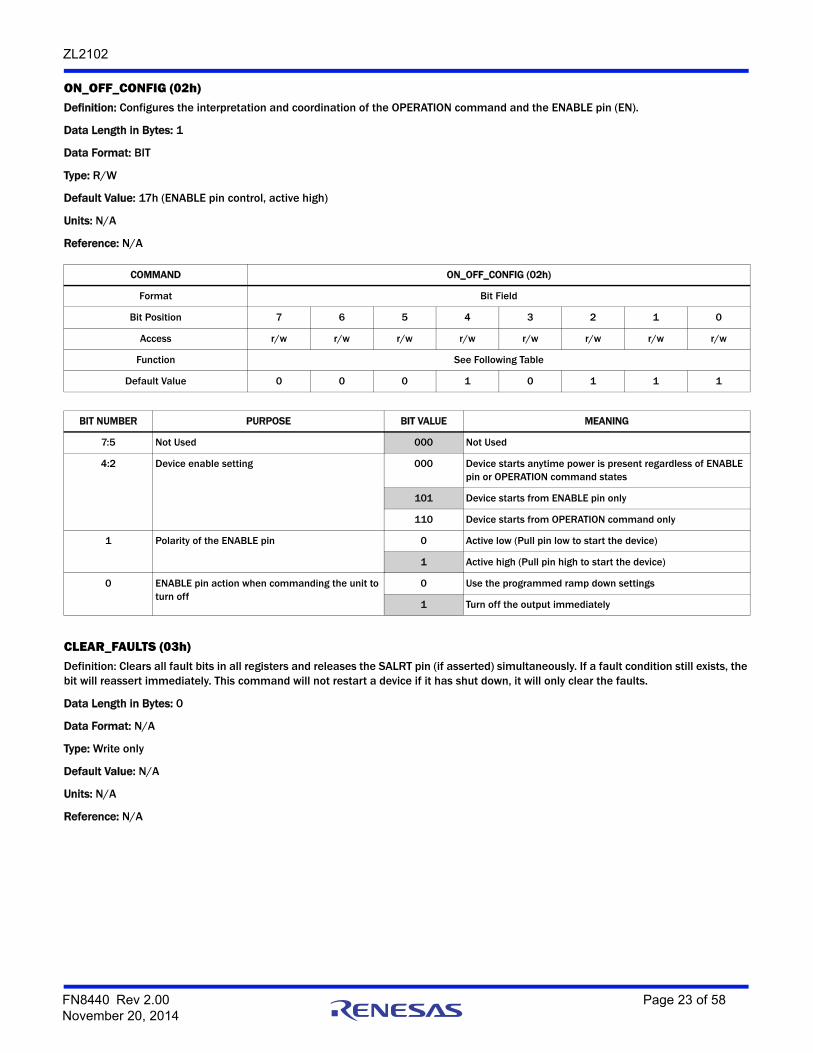
ZL2102
ON_OFF_CONFIG (02h)Definition: Configures the interpretation and coordination of the OPERATION command and the ENABLE pin (EN).
Data Length in Bytes: 1
Data Format: BIT
Type: R/W
Default Value: 17h (ENABLE pin control, active high)
Units: N/A
Reference: N/A
CLEAR_FAULTS (03h)Definition: Clears all fault bits in all registers and releases the SALRT pin (if asserted) simultaneously. If a fault condition still exists, the bit will reassert immediately. This command will not restart a device if it has shut down, it will only clear the faults.
Data Length in Bytes: 0
Data Format: N/A
Type: Write only
Default Value: N/A
Units: N/A
Reference: N/A
COMMAND ON_OFF_CONFIG (02h)
Format Bit Field
Bit Position 7 6 5 4 3 2 1 0
Access r/w r/w r/w r/w r/w r/w r/w r/w
Function See Following Table
Default Value 0 0 0 1 0 1 1 1
BIT NUMBER PURPOSE BIT VALUE MEANING
7:5 Not Used 000 Not Used
4:2 Device enable setting 000 Device starts anytime power is present regardless of ENABLE pin or OPERATION command states
101 Device starts from ENABLE pin only
110 Device starts from OPERATION command only
1 Polarity of the ENABLE pin 0 Active low (Pull pin low to start the device)
1 Active high (Pull pin high to start the device)
0 ENABLE pin action when commanding the unit to turn off
0 Use the programmed ramp down settings
1 Turn off the output immediately
FN8440 Rev 2.00 Page 23 of 58November 20, 2014
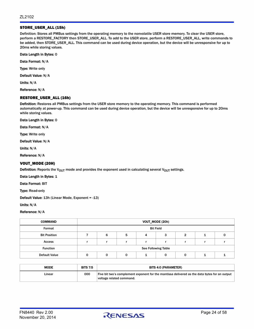
ZL2102
STORE_USER_ALL (15h)Definition: Stores all PMBus settings from the operating memory to the nonvolatile USER store memory. To clear the USER store, perform a RESTORE_FACTORY then STORE_USER_ALL. To add to the USER store, perform a RESTORE_USER_ALL, write commands to be added, then STORE_USER_ALL. This command can be used during device operation, but the device will be unresponsive for up to 20ms while storing values.
Data Length in Bytes: 0
Data Format: N/A
Type: Write only
Default Value: N/A
Units: N/A
Reference: N/A
RESTORE_USER_ALL (16h)Definition: Restores all PMBus settings from the USER store memory to the operating memory. This command is performed automatically at power-up. This command can be used during device operation, but the device will be unresponsive for up to 20ms while storing values.
Data Length in Bytes: 0
Data Format: N/A
Type: Write only
Default Value: N/A
Units: N/A
Reference: N/A
VOUT_MODE (20H)Definition: Reports the VOUT mode and provides the exponent used in calculating several VOUT settings.
Data Length in Bytes: 1
Data Format: BIT
Type: Read-only
Default Value: 13h (Linear Mode, Exponent = -13)
Units: N/A
Reference: N/A
COMMAND VOUT_MODE (20h)
Format Bit Field
Bit Position 7 6 5 4 3 2 1 0
Access r r r r r r r r
Function See Following Table
Default Value 0 0 0 1 0 0 1 1
MODE BITS 7:5 BITS 4:0 (PARAMETER)
Linear 000 Five bit two’s complement exponent for the mantissa delivered as the data bytes for an output voltage related command.
FN8440 Rev 2.00 Page 24 of 58November 20, 2014

ZL2102
VOUT_COMMAND (21h)Definition: This command sets or reports the target output voltage. The integer value is multiplied by 2 raised to the power of VOUT_MODE. This command cannot be set to be higher than the value of VOUT_MAX. This command can be written while the device is enabled, but the adjusted value must be within 10% of the value that was selected prior to enable.
Data Length in Bytes: 2
Data Format: L16u.
Type: R/W
Default Value: Pin strap setting (VSET)
Units: Volts
Equation: VOUT = VOUT_COMMAND×2-13
Range: 0.6V to 5.5V or the value of VOUT_MAX
Reference: N/A
Example: VOUT_MODE = 13h (Since the value is 5-bit signed 13h = -13)
VOUT_COMMAND = 699Ah = 27,034
Target voltage equals: 27034× 2-13 = 3.3V
VOUT_MAX (24h)Definition: The VOUT_ MAX command sets an upper limit on the output voltage the unit can command regardless of any other commands or combinations. The intent of this command is to provide a safeguard against a user accidentally setting the output voltage to a possibly destructive level rather than to be the primary output overprotection. If a VOUT_COMMAND is sent with a value higher than VOUT_MAX, the device will set the output voltage to VOUT_MAX. The initial value of VOUT_MAX is 110% of the pin strap value of VOUT.
Data Length in Bytes: 2
Data Format: L16u
Type: R/W
Default Value: 1.10 x VOUT_COMMAND pin strap setting
Units: Volts
Equation: VOUT max = VOUT_MAX×2-13
Range: 0V to 5.5V
Reference: N/A
COMMAND VOUT_COMMAND (21h)
Format Linear, unsigned binary
Bit Position 15 14 13 12 11 10 9 8 7 6 5 4 3 2 1 0
Access r/w r/w r/w r/w r/w r/w r/w r/w r/w r/w r/w r/w r/w r/w r/w r/w
Default Value Pin strap setting
COMMAND VOUT_MAX (24h)
Format Linear, unsigned binary
Bit Position 15 14 13 12 11 10 9 8 7 6 5 4 3 2 1 0
Access r/w r/w r/w r/w r/w r/w r/w r/w r/w r/w r/w r/w r/w r/w r/w r/w
Default Value 1.10 x VOUT_COMMAND Pin Strap Setting
FN8440 Rev 2.00 Page 25 of 58November 20, 2014

ZL2102
VOUT_MARGIN_HIGH (25h)Definition: Sets the value of the VOUT when OPERATION or the MGN pin is set for “margin high”. This command can be written while the device is enabled, but the adjusted value must be within 10% of the value of VOUT that was selected prior to enable.
Data Length in Bytes: 2
Data Format: L16u
Type: R/W
Default value: 1.05 x VOUT_COMMAND pin strap setting
Units: Volts
Equation: VOUT_MARGIN_HIGH = Y×2N
Range: 0.54V to the value of VOUT_MAX
Reference: N/A
VOUT_MARGIN_LOW (26h)Definition: Sets the value of the VOUT when OPERATION or the MGN pin is set for “margin low”. This command can be written while the device is enabled, but the adjusted value must be within 10% of the value of VOUT that was selected prior to enable.
Data Length in Bytes: 2
Data Format: L16u
Type: R/W
Default value: 0.95 x VOUT_COMMAND pin strap setting
Units: Volts
Equation: VOUT_MARGIN_LOW = Y×2N
Range: 0.54V to the value of VOUT_MAX
Reference: N/A
COMMAND VOUT_MARGIN_HIGH (25h)
Format Linear, unsigned binary
Bit Position 15 14 13 12 11 10 9 8 7 6 5 4 3 2 1 0
Access r/w r/w r/w r/w r/w r/w r/w r/w r/w r/w r/w r/w r/w r/w r/w r/w
Default Value 1.05 x VOUT_COMMAND
COMMAND VOUT_MARGIN_LOW (26h)
Format Linear, unsigned binary
Bit Position 15 14 13 12 11 10 9 8 7 6 5 4 3 2 1 0
Access r/w r/w r/w r/w r/w r/w r/w r/w r/w r/w r/w r/w r/w r/w r/w r/w
Default Value 0.95 x VOUT_COMMAND
FN8440 Rev 2.00 Page 26 of 58November 20, 2014

ZL2102
VOUT_TRANSITION_RATE (27h)Definition: Sets the rate at which the output should change voltage when the device receives an OPERATION command (Margin High, Margin Low) or VOUT_COMMAND command that causes the output voltage to change. The maximum possible positive value of the two data bytes indicates that the device should make the transition as quickly as possible.
Data Length in Bytes: 2
Data Format: L11
Type: R/W
Default value: B200h (0.5V/ms)
Units: V/ms
Equation: VOUT_TRANSITION_RATE = Y×2N
Range: 0.1V/ms to 2V/ms
Reference: N/A
FREQUENCY_SWITCH (33h)Definition: Sets the switching frequency of the device. Initial default value is defined by a pin strap and this value can be overridden by writing this command. If an external SYNC is utilized, this value should be set as close as possible to the external clock value. The output must be disabled when writing this command.
Data Length in Bytes: 2
Data Format: L11
Type: R/W
Default Value: Pin strap setting (SYNC)
Units: kHz
Equation: FREQUENCY_SWITCH = Y×2N
Range: 200kHz to 1MHz
Reference: N/A
COMMAND VOUT_TRANSITION_RATE (27h)
Format Linear, two’s complement binary
Bit Position 15 14 13 12 11 10 9 8 7 6 5 4 3 2 1 0
Access r/w r/w r/w r/w r/w r/w r/w r/w r/w r/w r/w r/w r/w r/w r/w r/w
Function Signed Exponent, N Signed Mantissa, Y
Default Value 1 0 1 1 0 0 1 0 0 0 0 0 0 0 0 0
COMMAND FREQUENCY_SWITCH (33h)
Format Linear, two’s complement binary
Bit Position 15 14 13 12 11 10 9 8 7 6 5 4 3 2 1 0
Access r/w r/w r/w r/w r/w r/w r/w r/w r/w r/w r/w r/w r/w r/w r/w r/w
Function Signed Exponent, N Signed Mantissa, Y
Default Value Pin Strapped Value
FN8440 Rev 2.00 Page 27 of 58November 20, 2014
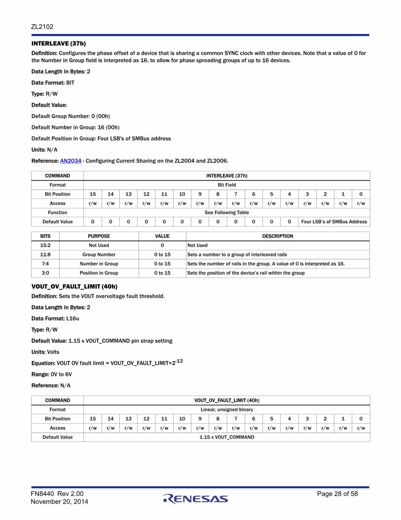
ZL2102
INTERLEAVE (37h)Definition: Configures the phase offset of a device that is sharing a common SYNC clock with other devices. Note that a value of 0 for the Number in Group field is interpreted as 16, to allow for phase spreading groups of up to 16 devices.
Data Length in Bytes: 2
Data Format: BIT
Type: R/W
Default Value:
Default Group Number: 0 (00h)
Default Number in Group: 16 (00h)
Default Position in Group: Four LSB's of SMBus address
Units: N/A
Reference: AN2034 - Configuring Current Sharing on the ZL2004 and ZL2006.
VOUT_OV_FAULT_LIMIT (40h)Definition: Sets the VOUT overvoltage fault threshold.
Data Length in Bytes: 2
Data Format: L16u
Type: R/W
Default Value: 1.15 x VOUT_COMMAND pin strap setting
Units: Volts
Equation: VOUT OV fault limit = VOUT_OV_FAULT_LIMIT×2-13
Range: 0V to 6V
Reference: N/A
COMMAND INTERLEAVE (37h)
Format Bit Field
Bit Position 15 14 13 12 11 10 9 8 7 6 5 4 3 2 1 0
Access r/w r/w r/w r/w r/w r/w r/w r/w r/w r/w r/w r/w r/w r/w r/w r/w
Function See Following Table
Default Value 0 0 0 0 0 0 0 0 0 0 0 0 Four LSB’s of SMBus Address
BITS PURPOSE VALUE DESCRIPTION
15:2 Not Used 0 Not Used
11:8 Group Number 0 to 15 Sets a number to a group of interleaved rails
7:4 Number in Group 0 to 15 Sets the number of rails in the group. A value of 0 is interpreted as 16.
3:0 Position in Group 0 to 15 Sets the position of the device’s rail within the group
COMMAND VOUT_OV_FAULT_LIMIT (40h)
Format Linear, unsigned binary
Bit Position 15 14 13 12 11 10 9 8 7 6 5 4 3 2 1 0
Access r/w r/w r/w r/w r/w r/w r/w r/w r/w r/w r/w r/w r/w r/w r/w r/w
Default Value 1.15 x VOUT_COMMAND
FN8440 Rev 2.00 Page 28 of 58November 20, 2014
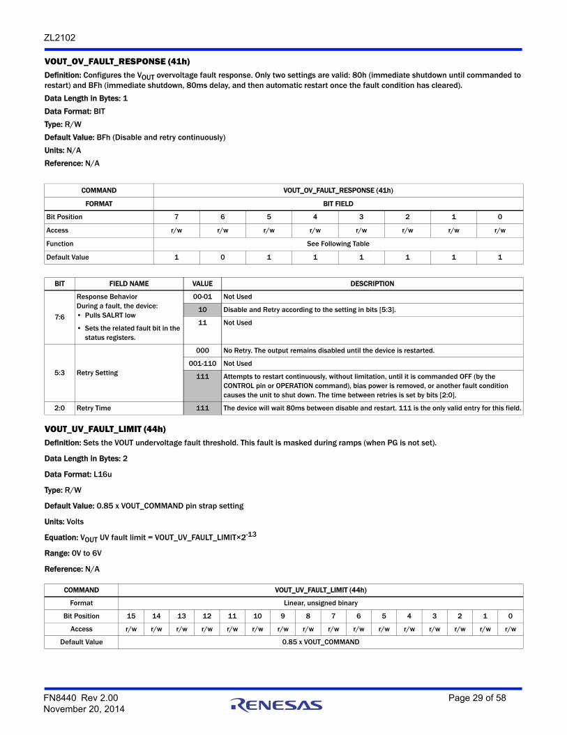
ZL2102
VOUT_OV_FAULT_RESPONSE (41h)Definition: Configures the VOUT overvoltage fault response. Only two settings are valid: 80h (immediate shutdown until commanded to restart) and BFh (immediate shutdown, 80ms delay, and then automatic restart once the fault condition has cleared).
Data Length in Bytes: 1
Data Format: BIT
Type: R/W
Default Value: BFh (Disable and retry continuously)
Units: N/A
Reference: N/A
VOUT_UV_FAULT_LIMIT (44h)Definition: Sets the VOUT undervoltage fault threshold. This fault is masked during ramps (when PG is not set).
Data Length in Bytes: 2
Data Format: L16u
Type: R/W
Default Value: 0.85 x VOUT_COMMAND pin strap setting
Units: Volts
Equation: VOUT UV fault limit = VOUT_UV_FAULT_LIMIT×2-13
Range: 0V to 6V
Reference: N/A
COMMAND VOUT_OV_FAULT_RESPONSE (41h)
FORMAT BIT FIELD
Bit Position 7 6 5 4 3 2 1 0
Access r/w r/w r/w r/w r/w r/w r/w r/w
Function See Following Table
Default Value 1 0 1 1 1 1 1 1
BIT FIELD NAME VALUE DESCRIPTION
7:6
Response Behavior During a fault, the device:• Pulls SALRT low
• Sets the related fault bit in the status registers.
00-01 Not Used
10 Disable and Retry according to the setting in bits [5:3].
11 Not Used
5:3 Retry Setting
000 No Retry. The output remains disabled until the device is restarted.
001-110 Not Used
111 Attempts to restart continuously, without limitation, until it is commanded OFF (by the CONTROL pin or OPERATION command), bias power is removed, or another fault condition causes the unit to shut down. The time between retries is set by bits [2:0].
2:0 Retry Time 111 The device will wait 80ms between disable and restart. 111 is the only valid entry for this field.
COMMAND VOUT_UV_FAULT_LIMIT (44h)
Format Linear, unsigned binary
Bit Position 15 14 13 12 11 10 9 8 7 6 5 4 3 2 1 0
Access r/w r/w r/w r/w r/w r/w r/w r/w r/w r/w r/w r/w r/w r/w r/w r/w
Default Value 0.85 x VOUT_COMMAND
FN8440 Rev 2.00 Page 29 of 58November 20, 2014

ZL2102
VOUT_UV_FAULT_RESPONSE (45h)Definition: Configures the VOUT undervoltage fault response. Only two settings are valid: 80h (immediate shutdown until commanded to restart) and BFh (immediate shutdown, 80ms delay, and then automatic restart once the fault condition has cleared).
Data Length in Bytes: 1
Data Format: BIT
Type: R/W
Default Value: BFh (Disable and retry continuously)
Units: N/A
Reference: N/A
IOUT_OC_FAULT_LIMIT (46h)Definition: Sets the IOUT peak overcurrent fault threshold. For down-slope sensing, this corresponds to the first current sample after the Current Sense Blanking Time has expired during the (1-D) time interval. For up-slope sensing, this corresponds to the last current sample of the D time interval. This feature shares the OC fault bit operation (in STATUS_IOUT) and OC fault response with IOUT_AVG_OC_FAULT_LIMIT.
Data Length in Bytes: 2
Data Format: L11
Type: R/W
Default Value: D240h (9A)
Units: A
Equation: IOUT_OC_FAULT_LIMIT = Y×2N
Range: 0A to 9A
Reference: N/A
COMMAND VOUT_UV_FAULT_RESPONSE (45h)
FORMAT BIT FIELD
Bit Position 7 6 5 4 3 2 1 0
Access r/w r/w r/w r/w r/w r/w r/w r/w
Function See Following Table
Default Value 1 0 1 1 1 1 1 1
BIT FIELD NAME VALUE DESCRIPTION
7:6
Response Behavior During a fault, the device:• Pulls SALRT low
• Sets the related fault bit in the status registers.
00-01 Not Used
10 Disable and Retry according to the setting in bits [5:3].
11 Not Used
5:3 Retry Setting
000 No Retry. The output remains disabled until the device is restarted.
001-110 Not Used
111 Attempts to restart continuously, without limitation, until it is commanded OFF (by the CONTROL pin or OPERATION command), bias power is removed, or another fault condition causes the unit to shut down. The time between retries is set by bits [2:0].
2:0 Retry Time 111 The device will wait 80ms between disable and restart. 111 is the only valid entry for this field.
COMMAND IOUT_OC_FAULT_LIMIT (46h)
Format Linear, two’s complement binary
Bit Position 15 14 13 12 11 10 9 8 7 6 5 4 3 2 1 0
Access r/w r/w r/w r/w r/w r/w r/w r/w r/w r/w r/w r/w r/w r/w r/w r/w
Function Signed Exponent, N Signed Mantissa, Y
Default Value 1 1 0 1 0 0 1 0 0 1 0 0 0 0 0 0
FN8440 Rev 2.00 Page 30 of 58November 20, 2014

ZL2102
IOUT_UC_FAULT_LIMIT (4Bh)Definition: Sets the IOUT valley undercurrent fault threshold. For down-slope sensing, this corresponds to the last current sample of the (1-D) time interval. For up-slope sensing, this corresponds to the first current sample of the D time interval, excluding the Current Sense Blanking time (which occurs at the beginning of the D interval). This feature shares the UC fault bit operation (in STATUS_IOUT) and UC fault response with IOUT_AVG_UC_FAULT_LIMIT.
Data Length in Bytes: 2
Data Format: L11
Type: R/W
Default Value: D5C0h (-9A)
Units: A
Equation: IOUT_OC_FAULT_LIMIT = Y×2N
Range: 0A to -9A
Reference: N/A
OT_FAULT_LIMIT (4Fh)Definition: Sets the over temperature fault threshold. Note that the temperature must drop below OT_WARN_LIMIT before the device will automatically restart.
Data Length in Bytes: 2
Data Format: L11
Type: R/W
Default Value: EBE8h (+125°C)
Units: Celsius
Equation: OT_FAULT_LIMIT = Y×2N
Range: 0°C to +125°C
Reference: N/A
COMMAND IOUT_UC_FAULT_LIMIT (4Bh)
Format Linear, two’s complement binary
Bit Position 15 14 13 12 11 10 9 8 7 6 5 4 3 2 1 0
Access r/w r/w r/w r/w r/w r/w r/w r/w r/w r/w r/w r/w r/w r/w r/w r/w
Function Signed Exponent, N Signed Mantissa, Y
Default Value 1 1 0 1 0 1 0 1 1 1 0 0 0 0 0 0
COMMAND OT_FAULT_LIMIT (4Fh)
Format Linear, two’s complement binary
Bit Position 15 14 13 12 11 10 9 8 7 6 5 4 3 2 1 0
Access r/w r/w r/w r/w r/w r/w r/w r/w r/w r/w r/w r/w r/w r/w r/w r/w
Function Signed Exponent, N Signed Mantissa, Y
Default Value 1 1 1 0 1 0 1 1 1 1 1 0 1 0 0 0
FN8440 Rev 2.00 Page 31 of 58November 20, 2014
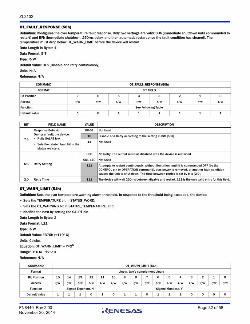
ZL2102
OT_FAULT_RESPONSE (50h)Definition: Configures the over temperature fault response. Only two settings are valid: 80h (immediate shutdown until commanded to restart) and BFh (immediate shutdown, 250ms delay, and then automatic restart once the fault condition has cleared). The temperature must drop below OT_WARN_LIMIT before the device will restart.
Data Length in Bytes: 1
Data Format: BIT
Type: R/W
Default Value: BFh (Disable and retry continuously)
Units: N/A
Reference: N/A
OT_WARN_LIMIT (51h)Definition: Sets the over temperature warning alarm threshold. In response to the threshold being exceeded, the device:
• Sets the TEMPERATURE bit in STATUS_WORD,
• Sets the OT_WARNING bit in STATUS_TEMPERATURE, and
• Notifies the host by setting the SALRT pin.
Data Length in Bytes: 2
Data Format: L11
Type: R/W
Default Value: EB70h (+110°C)
Units: Celsius
Equation: OT_WARN_LIMIT = Y×2N
Range: 0°C to +125°C
Reference: N/A
COMMAND OT_FAULT_RESPONSE (50h)
FORMAT BIT FIELD
Bit Position 7 6 5 4 3 2 1 0
Access r/w r/w r/w r/w r/w r/w r/w r/w
Function See Following Table
Default Value 1 0 1 1 1 1 1 1
BIT FIELD NAME VALUE DESCRIPTION
7:6
Response Behavior During a fault, the device:• Pulls SALRT low
• Sets the related fault bit in the status registers.
00-01 Not Used
10 Disable and Retry according to the setting in bits [5:3].
11 Not Used
5:3 Retry Setting
000 No Retry. The output remains disabled until the device is restarted.
001-110 Not Used
111 Attempts to restart continuously, without limitation, until it is commanded OFF (by the CONTROL pin or OPERATION command), bias power is removed, or another fault condition causes the unit to shut down. The time between retries is set by bits [2:0].
2:0 Retry Time 111 The device will wait 250ms between disable and restart. 111 is the only valid entry for this field.
COMMAND OT_WARN_LIMIT (51h)
Format Linear, two’s complement binary
Bit Position 15 14 13 12 11 10 9 8 7 6 5 4 3 2 1 0
Access r/w r/w r/w r/w r/w r/w r/w r/w r/w r/w r/w r/w r/w r/w r/w r/w
Function Signed Exponent, N Signed Mantissa, Y
Default Value 1 1 1 0 1 0 1 1 0 1 1 1 0 0 0 0
FN8440 Rev 2.00 Page 32 of 58November 20, 2014

ZL2102
UT_WARN_LIMIT (52h)Definition: Sets the under-temperature warning alarm threshold. In response to the threshold being exceeded, the device:
• Sets the TEMPERATURE bit in STATUS_WORD,
• Sets the UT_WARNING bit in STATUS_TEMPERATURE, and
• Notifies the host by setting the SALRT pin.
Data Length in Bytes: 2
Data Format: L11
Type: R/W
Default Value: E4E0h (-50°C)
Units: Celsius
Equation: UT_WARN_LIMIT = Y×2N
Range: -55°C to +25°C
Reference: N/A
UT_FAULT_LIMIT (53h)Definition: Sets the under-temperature fault threshold. Note that the temperature must rise above UT_WARN_LIMIT before the device will automatically restart.
Data Length in Bytes: 2
Data Format: L11
Type: R/W
Default Value: E490h (-55°C)
Units: Celsius
Equation: UT_FAULT_LIMIT = Y×2N
Range: -55°C to +25°C
Reference: N/A
UT_FAULT_RESPONSE (54h)Definition: Configures the under-temperature fault response. Only two settings are valid: 80h (immediate shutdown until commanded to restart) and BFh (immediate shutdown, 250ms delay, and then automatic restart once the fault condition has cleared). The temperature must rise above UT_WARN_LIMIT before the device will automatically restart.
Data Length in Bytes: 1
Data Format: BIT
Type: R/W
Default Value: BFh (Disable and retry continuously)
Units: N/A
Reference: N/A
COMMAND UT_WARN_LIMIT (52h)
Format Linear, two’s complement binary
Bit Position 15 14 13 12 11 10 9 8 7 6 5 4 3 2 1 0
Access r/w r/w r/w r/w r/w r/w r/w r/w r/w r/w r/w r/w r/w r/w r/w r/w
Function Signed Exponent, N Signed Mantissa, Y
Default Value 1 1 1 0 0 1 0 0 1 1 1 0 0 0 0 0
COMMAND UT_FAULT_LIMIT (53h)
Format Linear, two’s complement binary
Bit Position 15 14 13 12 11 10 9 8 7 6 5 4 3 2 1 0
Access r/w r/w r/w r/w r/w r/w r/w r/w r/w r/w r/w r/w r/w r/w r/w r/w
Function Signed Exponent, N Signed Mantissa, Y
Default Value 1 1 1 0 0 1 0 0 1 0 0 1 0 0 0 0
FN8440 Rev 2.00 Page 33 of 58November 20, 2014

ZL2102
VIN_OV_FAULT_LIMIT (55h)Definition: Sets the VIN overvoltage fault threshold.
Data Length in Bytes: 2
Data Format: L11
Type: R/W
Default Value: D380h (14V)
Units: Volts
Equation: VIN_OV_FAULT_LIMIT = Y×2N
Range: 4.5V to 16V
Reference: N/A
VIN_OV_FAULT_RESPONSE (56h)Definition: Configures the VIN overvoltage fault response as defined by the following table. Only two settings are valid: 80h (immediate shutdown until commanded to restart) and BFh (immediate shutdown, 80ms delay, and then automatic restart once the fault condition has cleared).
Data Length in Bytes: 1
Data Format: BIT
Type: R/W
Default Value: BFh (Disable and retry continuously)
Units: N/A
Reference: N/A
COMMAND UT_FAULT_RESPONSE (54h)
FORMAT BIT FIELD
Bit Position 7 6 5 4 3 2 1 0
Access r/w r/w r/w r/w r/w r/w r/w r/w
Function See Following Table
Default Value 1 0 1 1 1 1 1 1
BIT FIELD NAME VALUE DESCRIPTION
7:6
Response Behavior During a fault, the device:• Pulls SALRT low
• Sets the related fault bit in the status registers.
00-01 Not Used
10 Disable and Retry according to the setting in bits [5:3].
11 Not Used
5:3 Retry Setting
000 No Retry. The output remains disabled until the device is restarted.
001-110 Not Used
111 Attempts to restart continuously, without limitation, until it is commanded OFF (by the CONTROL pin or OPERATION command), bias power is removed, or another fault condition causes the unit to shut down. The time between retries is set by bits [2:0].
2:0 Retry Time 111 The device will wait 250ms between disable and restart. 111 is the only valid entry for this field.
COMMAND VIN_OV_FAULT_LIMIT (55h)
Format Linear, two’s complement binary
Bit Position 15 14 13 12 11 10 9 8 7 6 5 4 3 2 1 0
Access r/w r/w r/w r/w r/w r/w r/w r/w r/w r/w r/w r/w r/w r/w r/w r/w
Function Signed Exponent, N Signed Mantissa, Y
Default Value 1 1 0 1 0 0 1 1 1 0 0 0 0 0 0 0
FN8440 Rev 2.00 Page 34 of 58November 20, 2014

ZL2102
VIN_OV_WARN_LIMIT (57h)Definition: Sets the VIN overvoltage warning threshold as defined by the following table. In response to the OV_WARN_LIMIT being exceeded, the device:
• Sets the NONE OF THE ABOVE and INPUT bits in STATUS_WORD
• Sets the VIN_OV_WARNING bit in STATUS_INPUT, and
• Notifies the host by setting the SALRT pin.
Data Length in Bytes: 2
Data Format: L11
Type: R/W
Default Value: D360h (13.5V)
Units: Volts
Equation: VIN_OV_FAULT_LIMIT = Y×2N
Range: 4.5V to 16V
Reference: N/A
COMMAND VIN_OV_FAULT_RESPONSE (56h)
FORMAT BIT FIELD
Bit Position 7 6 5 4 3 2 1 0
Access r/w r/w r/w r/w r/w r/w r/w r/w
Function See Following Table
Default Value 1 0 1 1 1 1 1 1
BIT FIELD NAME VALUE DESCRIPTION
7:6
Response Behavior During a fault, the device:• Pulls SALRT low
• Sets the related fault bit in the status registers.
00-01 Not Used
10 Disable and Retry according to the setting in bits [5:3].
11 Not Used
5:3 Retry Setting
000 No Retry. The output remains disabled until the device is restarted.
001-110 Not Used
111 Attempts to restart continuously, without limitation, until it is commanded OFF (by the CONTROL pin or OPERATION command), bias power is removed, or another fault condition causes the unit to shut down. The time between retries is set by bits [2:0].
2:0 Retry Time 111 The device will wait 80ms between disable and restart. 111 is the only valid entry for this field.
COMMAND VIN_OV_WARN_LIMIT (57h)
Format Linear, two’s complement binary
Bit Position 15 14 13 12 11 10 9 8 7 6 5 4 3 2 1 0
Access r/w r/w r/w r/w r/w r/w r/w r/w r/w r/w r/w r/w r/w r/w r/w r/w
Function Signed Exponent, N Signed Mantissa, Y
Default Value 1 1 0 1 0 0 1 1 0 1 1 0 0 0 0 0
FN8440 Rev 2.00 Page 35 of 58November 20, 2014

ZL2102
VIN_UV_WARN_LIMIT (58h)Definition: Sets the VIN undervoltage warning threshold. If a VIN_UV_FAULT occurs, the input voltage must rise above VIN_UV_WARN_LIMIT to clear the fault, which provides hysteresis to the fault threshold. In response to the UV_WARN_LIMIT being exceeded, the device:
• Sets the NONE OF THE ABOVE and INPUT bits in STATUS_WORD,
• Sets the VIN_UV_WARNING bit in STATUS_INPUT, and
• Notifies the host by setting the SALRT pin.
Data Length in Bytes: 2
Data Format: L11
Type: R/W
Default Value: 1.03 x VIN_UV_FAULT_LIMIT pin strap setting
Units: V
Equation: VIN_UV_WARN_LIMIT = Y×2N
Range: 4.5V to 16V
Reference: N/A
VIN_UV_FAULT_LIMIT (59h)Definition: Sets the VIN undervoltage fault threshold. Also referred to as undervoltage lockout (UVLO).
Data Length in Bytes: 2
Data Format: L11
Type: R/W
Default Value: Pin strap setting (SS)
Units: Volts
Equation: VIN_UV_FAULT_LIMIT = Y×2N
Range: 4.5V to 16V
Reference: N/A
VIN_UV_FAULT_RESPONSE (5Ah)Definition: Configures the VIN undervoltage fault response as defined by the following table. Only two settings are valid: 80h (immediate shutdown until commanded to restart) and BFh (immediate shutdown, 80ms delay, and then automatic restart once the fault condition has cleared).
Data Length in Bytes: 1
Data Format: BIT
Type: R/W
Default Value: BFh (Disable and retry continuously)
Units: N/A
Reference: N/A
COMMAND VIN_UV_WARN_LIMIT (58h)
Format Linear, two’s complement binary
Bit Position 15 14 13 12 11 10 9 8 7 6 5 4 3 2 1 0
Access r/w r/w r/w r/w r/w r/w r/w r/w r/w r/w r/w r/w r/w r/w r/w r/w
Function Signed Exponent, N Signed Mantissa, Y
Default Value 1.03 x VIN_UV_FAULT_LIMIT
COMMAND VIN_UV_FAULT_LIMIT (59h)
Format Linear, two’s complement binary
Bit Position 15 14 13 12 11 10 9 8 7 6 5 4 3 2 1 0
Access r/w r/w r/w r/w r/w r/w r/w r/w r/w r/w r/w r/w r/w r/w r/w r/w
Function Signed Exponent, N Signed Mantissa, Y
Default Value Pin Strapped Value
FN8440 Rev 2.00 Page 36 of 58November 20, 2014
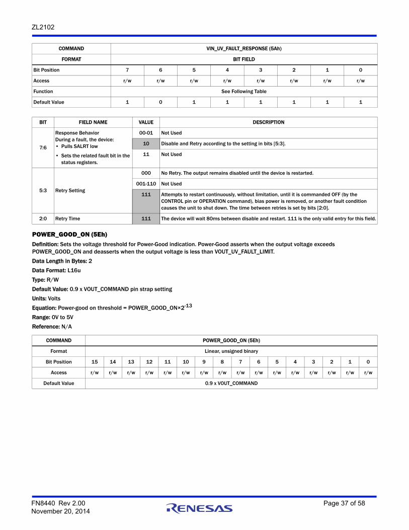
ZL2102
POWER_GOOD_ON (5Eh)Definition: Sets the voltage threshold for Power-Good indication. Power-Good asserts when the output voltage exceeds POWER_GOOD_ON and deasserts when the output voltage is less than VOUT_UV_FAULT_LIMIT.
Data Length in Bytes: 2
Data Format: L16u
Type: R/W
Default Value: 0.9 x VOUT_COMMAND pin strap setting
Units: Volts
Equation: Power-good on threshold = POWER_GOOD_ON×2-13
Range: 0V to 5V
Reference: N/A
COMMAND VIN_UV_FAULT_RESPONSE (5Ah)
FORMAT BIT FIELD
Bit Position 7 6 5 4 3 2 1 0
Access r/w r/w r/w r/w r/w r/w r/w r/w
Function See Following Table
Default Value 1 0 1 1 1 1 1 1
BIT FIELD NAME VALUE DESCRIPTION
7:6
Response Behavior During a fault, the device:• Pulls SALRT low
• Sets the related fault bit in the status registers.
00-01 Not Used
10 Disable and Retry according to the setting in bits [5:3].
11 Not Used
5:3 Retry Setting
000 No Retry. The output remains disabled until the device is restarted.
001-110 Not Used
111 Attempts to restart continuously, without limitation, until it is commanded OFF (by the CONTROL pin or OPERATION command), bias power is removed, or another fault condition causes the unit to shut down. The time between retries is set by bits [2:0].
2:0 Retry Time 111 The device will wait 80ms between disable and restart. 111 is the only valid entry for this field.
COMMAND POWER_GOOD_ON (5Eh)
Format Linear, unsigned binary
Bit Position 15 14 13 12 11 10 9 8 7 6 5 4 3 2 1 0
Access r/w r/w r/w r/w r/w r/w r/w r/w r/w r/w r/w r/w r/w r/w r/w r/w
Default Value 0.9 x VOUT_COMMAND
FN8440 Rev 2.00 Page 37 of 58November 20, 2014

ZL2102
TON_DELAY (60h)Definition: Sets the delay time from when the device is enabled to the start of VOUT rise.
Data Length in Bytes: 2
Data Format: L11
Type: R/W
Default Value: Pin strap setting (SS)
Units: ms
Equation: TON_DELAY = Y×2N
Range: 5ms to 30s
Reference: N/A
TON_RISE (61h)Definition: Sets the rise time of VOUT after ENABLE and TON_DELAY.
Data Length in Bytes: 2
Data Format: L11
Type: R/W
Default Value: Pin strap setting (SS)
Units: ms
Equation: TON_RISE = Y×2N
Range: 5ms to 200ms
Reference: N/A
TOFF_DELAY (64h)Definition: Sets the delay time from DISABLE to start of VOUT fall.
Data Length in Bytes: 2
Data Format: L11
Type: R/W
Default Value: 1 x TON_DELAY pin strap value
Units: ms
Equation: TON_DELAY = Y×2N
Range: 5ms to 30s
Reference: N/A
COMMAND TON_DELAY (60h)
Format Linear, two’s complement binary
Bit Position 15 14 13 12 11 10 9 8 7 6 5 4 3 2 1 0
Access r/w r/w r/w r/w r/w r/w r/w r/w r/w r/w r/w r/w r/w r/w r/w r/w
Function Signed Exponent, N Signed Mantissa, Y
Default Value Pin Strapped Value
COMMAND TON_RISE (61h)
Format Linear, two’s complement binary
Bit Position 15 14 13 12 11 10 9 8 7 6 5 4 3 2 1 0
Access r/w r/w r/w r/w r/w r/w r/w r/w r/w r/w r/w r/w r/w r/w r/w r/w
Function Signed Exponent, N Signed Mantissa, Y
Default Value Pin Strapped Value
FN8440 Rev 2.00 Page 38 of 58November 20, 2014

ZL2102
TOFF_FALL (65h)Definition: Sets the fall time for VOUT after DISABLE and TOFF_DELAY.
Data Length in Bytes: 2
Data Format: L11
Type: R/W
Default Value: 1 x TON_RISE pin strap setting
Units: ms
Equation: TOFF_FALL = Y×2N
Range: 5ms to 200ms
Reference: N/A
COMMAND TOFF_DELAY (64h)
Format Linear, two’s complement binary
Bit Position 15 14 13 12 11 10 9 8 7 6 5 4 3 2 1 0
Access r/w r/w r/w r/w r/w r/w r/w r/w r/w r/w r/w r/w r/w r/w r/w r/w
Function Signed Exponent, N Signed Mantissa, Y
Default Value 1 x TON_DELAY
COMMAND TOFF_FALL (65h)
Format Linear, two’s complement binary
Bit Position 15 14 13 12 11 10 9 8 7 6 5 4 3 2 1 0
Access r/w r/w r/w r/w r/w r/w r/w r/w r/w r/w r/w r/w r/w r/w r/w r/w
Function Signed Exponent, N Signed Mantissa, Y
Default Value 1 x TON_RISE
FN8440 Rev 2.00 Page 39 of 58November 20, 2014

ZL2102
STATUS_WORD (79h)Definition: Returns fault condition status information. Based on the information in these bytes, the host can get more information by reading the appropriate status registers. Status bits are only cleared by a forced restart or by writing to the CLEAR_FAULTS PMBus command.
Data Length in Bytes: 2
Data Format: BIT
Type: Read-only
Default Value: N/A
Units: N/A
Reference: N/A
COMMAND STATUS_WORD (79h)
Format Bit Field
Bit Position 15 14 13 12 11 10 9 8 7 6 5 4 3 2 1 0
Access r r r r r r r r r r r r r r r r
Function See Following Table
BIT NUMBER STATUS BIT NAME MEANING
15 VOUT An output voltage fault or warning has occurred.
14 IOUT An output current or output power fault or warning has occurred.
13 INPUT An input voltage, input current, or input power fault or warning has occurred.
12 MFG_SPECIFIC A manufacturer specific fault or warning has occurred.
11 POWER_GOOD # The POWER_GOOD signal, if present, is negated. (Note 12)
10 NOT USED
9 OTHER A bit in STATUS_VOUT, STATUS_IOUT,STATUS_MFR_SPECIFIC, or STATUS_VIN is set.
8 UNKNOWN A fault type not given in bits 15:1 of the STATUS_WORD has been detected.
7 BUSY A fault was declared because the device was busy and unable to respond.
6 OFF This bit is asserted if the unit is not providing power to the output, regardless of the reason, including simply not being enabled.
5 VOUT_OV_FAULT An output overvoltage fault has occurred.
4 IOUT_OC_FAULT An output overcurrent fault has occurred.
3 VIN_UV_FAULT An input undervoltage fault has occurred.
2 TEMPERATURE A temperature fault or warning has occurred.
1 CML A communications, memory or logic fault has occurred.
0 NONE OF THE ABOVE A fault or warning not listed in bits 7:1 has occurred.
NOTE:12. If the POWER_GOOD# bit is set, this indicates that the POWER_GOOD signal, if present, is signaling that the output power is not good.
FN8440 Rev 2.00 Page 40 of 58November 20, 2014

ZL2102
STATUS_VOUT (7Ah)Definition: Returns output voltage status information. Status bits are only cleared by a forced restart or by writing to the CLEAR_FAULTS PMBus command.
Data Length in Bytes: 1
Data Format: BIT
Type: Read-only
Default Value: N/A
Units: N/A
Reference: N/A
STATUS_IOUT (7Bh)Definition: Returns the output current status information. Status bits are only cleared by a forced restart or by writing to the CLEAR_FAULTS PMBus command.
Data Length in Bytes: 1
Data Format: BIT
Type: Read-only
Default Value: N/A
Units: N/A
Reference: N/A
COMMAND STATUS_VOUT (7Ah)
FORMAT BIT FIELD
Bit Position 7 6 5 4 3 2 1 0
Access r r r r r r r r
Function See Following Table
BIT NUMBER STATUS BIT NAME MEANING
7 VOUT_OV_FAULT Indicates an output overvoltage fault.
6:5 N/A These bits are not used.
4 VOUT_UV_FAULT Indicates an output undervoltage fault.
3:0 N/A These bits are not used.
COMMAND STATUS_IOUT (7Bh)
FORMAT BIT FIELD
Bit Position 7 6 5 4 3 2 1 0
Access r r r r r r r r
Function See Following Table
BIT NUMBER STATUS BIT NAME MEANING
7 IOUT_OC_FAULT Indicates an output overcurrent fault has occurred.
6:5 N/A These bits are not used.
4 IOUT_UC_FAULT Indicates an output undercurrent fault has occurred.
3:0 N/A These bits are not used.
FN8440 Rev 2.00 Page 41 of 58November 20, 2014
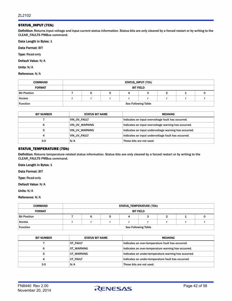
ZL2102
STATUS_INPUT (7Ch)Definition: Returns input voltage and input current status information. Status bits are only cleared by a forced restart or by writing to the CLEAR_FAULTS PMBus command.
Data Length in Bytes: 1
Data Format: BIT
Type: Read-only
Default Value: N/A
Units: N/A
Reference: N/A
STATUS_TEMPERATURE (7Dh)Definition: Returns temperature related status information. Status bits are only cleared by a forced restart or by writing to the CLEAR_FAULTS PMBus command.
Data Length in Bytes: 1
Data Format: BIT
Type: Read-only
Default Value: N/A
Units: N/A
Reference: N/A
COMMAND STATUS_INPUT (7Ch)
FORMAT BIT FIELD
Bit Position 7 6 5 4 3 2 1 0
Access r r r r r r r r
Function See Following Table
BIT NUMBER STATUS BIT NAME MEANING
7 VIN_OV_FAULT Indicates an input overvoltage fault has occurred.
6 VIN_OV_WARNING Indicates an input overvoltage warning has occurred.
5 VIN_UV_WARNING Indicates an input undervoltage warning has occurred.
4 VIN_UV_FAULT Indicates an input undervoltage fault has occurred.
3:0 N/A These bits are not used.
COMMAND STATUS_TEMPERATURE (7Dh)
FORMAT BIT FIELD
Bit Position 7 6 5 4 3 2 1 0
Access r r r r r r r r
Function See Following Table
BIT NUMBER STATUS BIT NAME MEANING
7 OT_FAULT Indicates an over-temperature fault has occurred.
6 OT_WARNING Indicates an over-temperature warning has occurred.
5 UT_WARNING Indicates an under-temperature warning has occurred.
4 UT_FAULT Indicates an under-temperature fault has occurred.
3:0 N/A These bits are not used.
FN8440 Rev 2.00 Page 42 of 58November 20, 2014
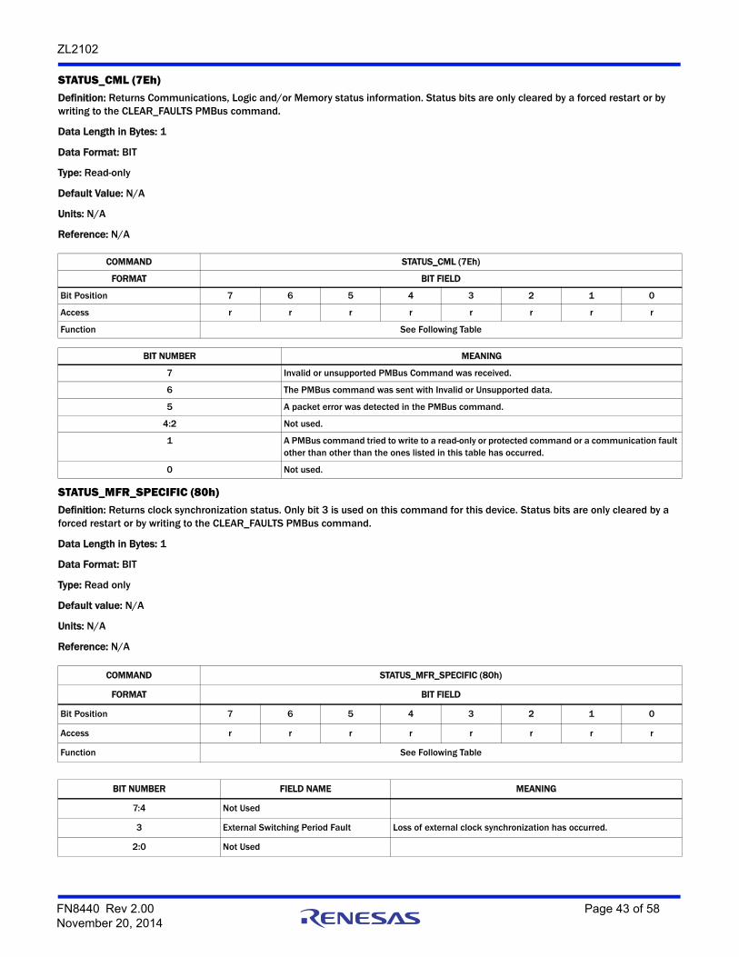
ZL2102
STATUS_CML (7Eh)Definition: Returns Communications, Logic and/or Memory status information. Status bits are only cleared by a forced restart or by writing to the CLEAR_FAULTS PMBus command.
Data Length in Bytes: 1
Data Format: BIT
Type: Read-only
Default Value: N/A
Units: N/A
Reference: N/A
STATUS_MFR_SPECIFIC (80h)Definition: Returns clock synchronization status. Only bit 3 is used on this command for this device. Status bits are only cleared by a forced restart or by writing to the CLEAR_FAULTS PMBus command.
Data Length in Bytes: 1
Data Format: BIT
Type: Read only
Default value: N/A
Units: N/A
Reference: N/A
COMMAND STATUS_CML (7Eh)
FORMAT BIT FIELD
Bit Position 7 6 5 4 3 2 1 0
Access r r r r r r r r
Function See Following Table
BIT NUMBER MEANING
7 Invalid or unsupported PMBus Command was received.
6 The PMBus command was sent with Invalid or Unsupported data.
5 A packet error was detected in the PMBus command.
4:2 Not used.
1 A PMBus command tried to write to a read-only or protected command or a communication fault other than other than the ones listed in this table has occurred.
0 Not used.
COMMAND STATUS_MFR_SPECIFIC (80h)
FORMAT BIT FIELD
Bit Position 7 6 5 4 3 2 1 0
Access r r r r r r r r
Function See Following Table
BIT NUMBER FIELD NAME MEANING
7:4 Not Used
3 External Switching Period Fault Loss of external clock synchronization has occurred.
2:0 Not Used
FN8440 Rev 2.00 Page 43 of 58November 20, 2014

ZL2102
READ_VIN (88h)Definition: Returns the input voltage reading.
Data Length in Bytes: 2
Data Format: L11
Type: Read-only
Default Value: N/A
Units: Volts
Equation: READ_VIN = Y×2N
Range: N/A
Reference: N/A
READ_VOUT (8Bh)Definition: Returns the output voltage reading.
Data Length in Bytes: 2
Data Format: L16u
Type: Read-only
Default Value: N/A
Units: Volts
Equation: Read VOUT = READ_VOUT×2-13
Reference: N/A
READ_IOUT (8Ch)Definition: Returns the output current reading.
Data Length in Bytes: 2
Data Format: L11
Type: Read-only
Default Value: N/A
Units: A
Equation: READ_IOUT = Y×2N
Range: N/A
Reference: N/A
COMMAND READ_VIN (88h)
FORMAT LINEAR, TWO'S COMPLEMENT BINARY
Bit Position 15 14 13 12 11 10 9 8 7 6 5 4 3 2 1 0
Access r r r r r r r r r r r r r r r r
Function Signed Exponent, N Signed Mantissa, Y
COMMAND READ_VOUT (8Bh)
Format Linear, unsigned binary
Bit Position 15 14 13 12 11 10 9 8 7 6 5 4 3 2 1 0
Access r r r r r r r r r r r r r r r r
COMMAND READ_IOUT (8Ch)
Format Linear, two’s complement binary
Bit Position 15 14 13 12 11 10 9 8 7 6 5 4 3 2 1 0
Access r r r r r r r r r r r r r r r r
Function Signed Exponent, N Signed Mantissa, Y
FN8440 Rev 2.00 Page 44 of 58November 20, 2014

ZL2102
READ_TEMPERATURE_1 (8Dh)Definition: Returns the temperature reading internal to the device.
Data Length in Bytes: 2
Data Format: L11
Type: Read-only
Default Value: N/A
Units: °C
Equation: READ_TEMPERATURE_1 = Y×2N
Range: N/A
Reference: N/A
READ_DUTY_CYCLE (94h)Definition: Reports the actual duty cycle of the converter during the enable state.
Data Length in Bytes: 2
Data Format: L11
Type: Read only
Default Value: N/A
Units: %
Equation: READ_DUTY_CYCLE = Y×2N
Range: N/A
Reference: N/A
READ_FREQUENCY (95h)Definition: Reports the actual switching frequency of the converter during the enable state.
Data Length in Bytes: 2
Data Format: L11
Type: Read only
Default Value: N/A
Units: kHz
Equation: READ_FREQUENCY = Y×2N
Range: N/A
Reference: N/A
COMMAND READ_TEMPERATURE_1 (8Dh)
Format Linear, two’s complement binary
Bit Position 15 14 13 12 11 10 9 8 7 6 5 4 3 2 1 0
Access r r r r r r r r r r r r r r r r
Function Signed Exponent, N Signed Mantissa, Y
COMMAND READ_DUTY_CYCLE (94h)
Format Linear, two’s complement binary
Bit Position 15 14 13 12 11 10 9 8 7 6 5 4 3 2 1 0
Access r r r r r r r r r r r r r r r r
Function Signed Exponent, N Signed Mantissa, Y
COMMAND READ_FREQUENCY (95h)
Format Linear, two’s complement binary
Bit Position 15 14 13 12 11 10 9 8 7 6 5 4 3 2 1 0
Access r r r r r r r r r r r r r r r r
Function Signed Exponent, N Signed Mantissa, Y
FN8440 Rev 2.00 Page 45 of 58November 20, 2014
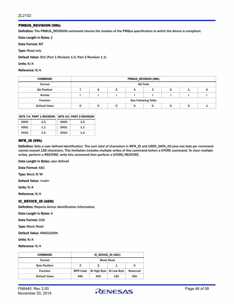
ZL2102
PMBUS_REVISION (98h)Definition: The PMBUS_REVISION command returns the revision of the PMBus specification to which the device is compliant.
Data Length in Bytes: 1
Data Format: BIT
Type: Read only
Default Value: 01h (Part 1 Revision 1.0, Part 2 Revision 1.1)
Units: N/A
Reference: N/A
MFR_ID (99h)Definition: Sets a user defined identification. The sum total of characters in MFR_ID and USER_DATA_00 plus one byte per command cannot exceed 128 characters. This limitation includes multiple writes of this command before a STORE command. To clear multiple writes, perform a RESTORE, write this command then perform a STORE/RESTORE.
Data Length in Bytes: user defined
Data Format: ASC
Type: Block R/W
Default Value: <null>
Units: N/A
Reference: N/A
IC_DEVICE_ID (ADH)Definition: Reports device identification information.
Data Length in Bytes: 4
Data Format: CUS
Type: Block Read
Default Value: 49A01200h
Units: N/A
Reference: N/A
COMMAND PMBUS_REVISION (98h)
Format Bit Field
Bit Position 7 6 5 4 3 2 1 0
Access r r r r r r r r
Function See Following Table
Default Value 0 0 0 0 0 0 0 1
BITS 7:4 PART 1 REVISION BITS 3:0 PART 2 REVISION
0000 1.0 0000 1.0
0001 1.1 0001 1.1
0010 1.2 0010 1.2
COMMAND IC_DEVICE_ID (ADh)
Format Block Read
Byte Position 3 2 1 0
Function MFR Code ID High Byte ID Low Byte Reserved
Default Value 49h A0h 12h 00h
FN8440 Rev 2.00 Page 46 of 58November 20, 2014

ZL2102
IC_DEVICE_REV (AEH)Definition: Reports device revision information.
Data Length in Bytes: 4
Data Format: CUS
Type: Block Read
Default Value:
Units: N/A
Reference: N/A
USER_DATA_00 (B0h)Definition: Sets a user defined data. The sum total of characters in MFR_ID and USER_DATA_00 plus one byte per command cannot exceed 128 characters. This limitation includes multiple writes of this command before a STORE command. To clear multiple writes, perform a RESTORE, write this command then perform a STORE/RESTORE.
Data Length in Bytes: user defined
Data Format: ASC
Type: Block R/W
Default Value: <null>
Units: N/A
Reference: N/A
AUTO_COMP_CONFIG (BCh)Definition: Configures the auto compensation algorithm.
Data Length in Bytes: 1
Data Format: BIT
Type: R/W
Default Value: Pin strap setting (FC)
Units: N/A
Reference: N/A
COMMAND IC_DEVICE_REV (AEh)
Format Block Read
Byte Position 3 2 1 0
Function Firmware Major
Firmware Minor
Factory Config
Reserved
Default Value 00h 00h 00h 00h
COMMAND AUTO_COMP_CONFIG (BCh)
Format Bit Field
Bit Position 7 6 5 4 3 2 1 0
Access r/w r/w r/w r/w r/w r/w r/w r/w
Function See Following Table
Default Value Pin Strapped Value
FN8440 Rev 2.00 Page 47 of 58November 20, 2014

ZL2102
AUTO_COMP_CONTROL (BDh)Definition: Writing the AUTO_COMP_CONTROL command will initiate the auto compensation algorithm, provided that it has been enabled in AUTO_COMP_CONFIG.
Data Length in Bytes: 0 Byte
Type: Write only
Default Value: N/A
Units: N/A
Reference: N/A
MFR_CONFIG (D0h)Definition: Configures several manufacturer-level features.
Data Length in Bytes: 2
Data Format: BIT
Type: R/W word
Default Value: 4801h
Units: N/A
Range: N/A
Reference: N/A
BIT FIELD NAME VALUE SETTING DESCRIPTION
7:4 Auto Comp Gain
0000 10%
Auto Comp Gain Percentage
0001 20%
0010 30%
0011 40%
0100 50%
0101 60%
0110 70%
0111 80%
1000 90%
1001 100%
3 Power-Good Assertion0 Use PG Delay Choose when PGOOD pin asserts, whether to use
PG DELAY or wait until after auto comp completes.
1 Assert after auto comp
2:1 Not Used 00
0 Auto Comp Mode0 Disabled Operational mode for auto comp. If disabled,
PID_TAPS is used for compensation1 Enabled
COMMAND MFR_CONFIG (D0h)
FORMAT BIT FIELD
Bit Position 15 14 13 12 11 10 9 8 7 6 5 4 3 2 1 0
Access r/w r/w r/w r/w r/w r/w r/w r/w r/w r/w r/w r/w r/w r/w r/w r/w
Function See Following Table
Default Value 0 1 0 0 1 0 0 0 0 0 0 0 0 0 0 1
BIT FIELD NAME VALUE SETTING DESCRIPTION
15:2 Not Used 01001000000000 Not Used Not Used
1 PGOOD Config0 Open Drain
Configuration of PGOOD pin1 Push-pull
0 SYNC Pin Config0 Open Drain
Configuration of SYNC pin1 Push-pull
FN8440 Rev 2.00 Page 48 of 58November 20, 2014

ZL2102
USER_CONFIG (D1h)Definition: Configures several user-level features.
Data Length in Bytes: 2
Data Format: BIT
Type: R/W
Default Value: Pin strap setting
Units: N/A
DDC_CONFIG (D3h)Definition: Configures the DDC bus.
Data Length in Bytes: 2
Data Format: BIT
Type: R/W
Default Value: Broadcast Group: 0; DDC ID: Lowest five bits of the SMBus Address.
Units: N/A
Reference: N/A
COMMAND USER_CONFIG (D1h)
Format Bit Field
Bit Position 15 14 13 12 11 10 9 8 7 6 5 4 3 2 1 0
Access r/w r/w r/w r/w r/w r/w r/w r/w r/w r/w r/w r/w r/w r/w r/w r/w
Function See Following Table
Default Value 0 0 0 0 0 0 0 0 0 Pin Strap 0 0 0 0 1
BIT FIELD NAME VALUE SETTING DESCRIPTION
12Alternate Ramp Down
0 Ramp Down Determines whether output follows TOFF_FALL time during ramp down or goes high impedance once VOUT_UV threshold is reached1 High-Z
11:9 Not Used 000
8 Fault Spreading Mode
0 0 = If sequencing is disabled, this device will ignore faults from other devices. If sequencing is enabled, the devices will sequence down from the failed device outward.1 = Faults received from any device selected by the DDC_GROUP command will cause this device to shut down immediately
1
7 Not Used 0
6SYNC Utilization Control
0 Auto-configure Auto-configure using the SYNC pin strap setting and FREQUENCY_SWITCH parameter
1 SYNC Setting Switch using external clock on the SYNC input pin
5 SYNC Output Control0 Input Only
Configuration setting of SYNC pin1 Output Internal Clock
4:1 Not Used 0000
0 Standby mode 0 Low Power Enter low power mode when output is disabled. Telemetry will not be available.
1 Monitor Monitor for faults when output is disabled.
COMMAND DDC_CONFIG (D3h)
Format Bit Field
Bit Position 15 14 13 12 11 10 9 8 7 6 5 4 3 2 1 0
Access r/w r/w r/w r/w r/w r/w r/w r/w r/w r/w r/w r/w r/w r/w r/w r/w
Function See Following Table
Default Value 0 0 0 0 0 0 0 0 0 0 0 Lowest 5 bits of SMBus Address
FN8440 Rev 2.00 Page 49 of 58November 20, 2014

ZL2102
POWER_GOOD_DELAY (D4h)Definition: Sets the delay applied between the output exceeding the PG threshold (POWER_GOOD_ON) and asserting the PG pin. The delay time can range from 1ms up to 30s. When auto comp is enabled and is set to assert the PG pin after completion, this command will be ignored.
Data Length in Bytes: 2
Data Format: L11
Type: R/W
Default Value: BA00h (1ms)
Units: ms
Equation: POWER_GOOD_DELAY = (Y×2N)
Range: 1ms to 30s
Reference: N/A
PID_TAPS (D5h)Definition: This command configures the control loop compensator coefficients. The PID algorithm implements the following Z-domain:
The coefficients A, B, and C are represented using a pseudo-floating point format similar to the VOUT parameters (with the addition of a sign bit), defined as Equation 15:
where M is a two-byte unsigned mantissa, S is a sign-bit, and E is a 7-bit two's-complement signed integer. The 9 byte data field is defined in the following table. S is stored as the MSB of the E byte.
BIT FIELD NAME VALUE SETTING DESCRIPTION
15:13 Not Used 0000 Not Used Not Used
12:8 Broadcast Group 0 to 31(00 to 1Fh)
0 Group number used for broadcast events (i.e., Broadcast Enable and Broadcast Margin). Set this number to the same value for all rails/devices that should respond to each other’s broadcasted event. This function is enabled by bits 15 and 14 in the MISC_CONFIG command.
7:6 Not Used 00 Not Used Not Used
5 DDC TX Inhibit1 Inhibited DDC Transmission Inhibited
0 Enabled DDC Transmission Enabled
4:0 DDC ID 0 to 31(00 to 1Fh)
Lowest 5 bits of the SMBus address
Sets the rail’s DDC ID for sequencing and fault spreading.
COMMAND POWER-GOOD_DELAY (D4h)
Format Linear, two’s complement binary
Bit Position 15 14 13 12 11 10 9 8 7 6 5 4 3 2 1 0
Access r/w r/w r/w r/w r/w r/w r/w r/w r/w r/w r/w r/w r/w r/w r/w r/w
Function Signed Exponent, N Signed Mantissa, Y
Default Value 1 0 1 1 1 0 1 0 0 0 0 0 0 0 0 0
A Bz1–
Cz2–
+ +
1 z1–
–-------------------------------------------- (EQ. 14)
A 1– S= 2E
M (EQ. 15)
FN8440 Rev 2.00 Page 50 of 58November 20, 2014

ZL2102
Data Length in Bytes: 9
Data Format: CUS
Type: Block R/W
Default Value:
Auto Comp Off, taps stored - (A, B, C) = stored values
Auto Comp Off, no taps stored - (A, B, C) correspond to (G, Q, fn) = (20dB, 2, fSW/10)
Auto Comp On - (A, B, C) = Auto Comp results
Units: N/A
Reference: AN2035 - Compensation Using CompZL™
SEQUENCE (E0h)Definition: Identifies the Rail DDC ID of the prequel and sequel rails when performing multi-rail sequencing. The device will enable its output when its EN or OPERATION enable state, as defined by ON_OFF_CONFIG, is set and the prequel device has issued a Power-Good event on the DDC bus. The device will disable its output (using the programmed delay values) when the sequel device has issued a Power-Down event on the DDC bus.
The data field is a two-byte value. The most-significant byte contains the 5-bit Rail DDC ID of the prequel device. The least-significant byte contains the 5-bit Rail DDC ID of the sequel device. The most significant bit of each byte contains the enable of the prequel or sequel mode. This command overrides the corresponding sequence configuration set by the CONFIG pin settings.
Data Length in Bytes: 2
Data Format: CUS
Type: R/W
Default Value: Pin strap setting (CFG)
Units: N/A
Reference: N/A
BYTE PURPOSE DEFINITION
8 Tap C-E Coefficient C exponent + S
7 Tap C-M [15:8] Coefficient C mantissa, high-byte
6 Tap C-M [7:0] Coefficient C mantissa, low-byte
5 Tap B-E Coefficient B exponent + S
4 Tap B-M [15:8] Coefficient B mantissa, high-byte
3 Tap B-M [7:0] Coefficient B mantissa, low-byte
2 Tap A-E Coefficient A exponent + S
1 Tap A-M [15:8] Coefficient A mantissa, high-byte
0 Tap A-M [7:0] Coefficient A mantissa, low-byte
NOTE: Data bytes are transmitted on the PMBus in the order of Byte 0 through Byte 8.
COMMAND SEQUENCE (E0h)
Format Custom
Bit Position 15 14 13 12 11 10 9 8 7 6 5 4 3 2 1 0
Access r/w r/w r/w r/w r/w r/w r/w r/w r/w r/w r/w r/w r/w r/w r/w r/w
Function See Following Table
Default Value Pin Strapped Value
BIT FIELD NAME VALUE SETTING DESCRIPTION
15 Prequel Enable0 Disable Disable, no prequel preceing this rail
1 Enable Enable, prequel to this rail is defined by bits 12:8
14:13 Reserved 0 Reserved Reserved
12:8 Prequel Rail DDC ID 0 to 31 DDC ID Set to the DDC ID of the prequel rail
FN8440 Rev 2.00 Page 51 of 58November 20, 2014

ZL2102
DDC_GROUP (E2h)Definition: Sets which rail DDC IDs are monitored for fault spreading information. The data sent is a 4-byte, 32-bit, bit vector where every bit represents a rail's DDC ID. Setting a bit to 1 will include that rail's DDC ID in the group. All DDC ID's that are selected will be monitored. If fault spread mode is enabled in USER_CONFIG (Bit 8 set to 1), the rail will respond to any fault spreading events within the group. The device will immediately shut down if one of its DDC_GROUP members fails. The device/rail will attempt its configured restart only after all devices/rails within the DDC_GROUP have cleared their faults.
Note: The device/rail's own DDC ID should not be set within the DDC_GROUP command for that device/rail.
All devices in a current share rail must shutdown for the rail to report a shutdown.
If fault spread mode is disabled in USER_CONFIG (Bit 8 cleared to 0), the device will perform a sequenced shutdown as defined by the SEQUENCE command setting. The rails/devices in a sequencing set only attempt their configured restart after all faults have cleared within the DDC_GROUP.
Data Length in Bytes: 4
Data Format: BIT
Type: R/W
Default Value: 00000000h
Units: N/A
Reference: N/A
DEVICE_ID (E4h)Definition: Returns the 16-byte (character) device identifier string.
Data Length in Bytes: 16
Data Format: ASC
Type: Block Read
Default Value: <part number/die revision/firmware revision>
Units: N/A
Reference: N/A
MFR_IOUT_OC_FAULT_RESPONSE (E5h)Definition: Configures the IOUT overcurrent fault response as defined by the following table. Only two settings are valid: 80h (immediate shutdown until commanded to restart) and BFh (immediate shutdown, 80ms delay, and then automatic restart once the fault condition has cleared). The command format is the same as the PMBus standard fault responses except that it sets the overcurrent status bit in STATUS_IOUT.
Data Length in Bytes: 1
Data Format: BIT
Type: R/W
Default Value: BFh (Disable and retry continuously)
Units: N/A
Reference: N/A
7 Sequel Enable0 Disable Disable, no sequel following this rail
1 Enable Enable, sequel to this rail is defined by bits 4:0
6:5 Reserved 0 Reserved Reserved
4:0 Sequel Rail DDC ID 0 to 31 DDC ID Set to the DDC ID of the sequel rail
COMMAND DDC_GROUP (E2h)
Format Bit Field
BitPosition
31 30 29 28 27 26 25 24 23 22 21 20 19 18 17 16 15 14 13 12 11 10 9 8 7 6 5 4 3 2 1 0
Access r/w r/w r/w r/w r/w r/w r/w r/w r/w r/w r/w r/w r/w r/w r/w r/w r/w r/w r/w r/w r/w r/w r/w r/w r/w r/w r/w r/w r/w r/w r/w r/w
DDC ID 31 30 29 28 27 26 25 24 23 22 21 20 19 18 17 16 15 14 13 12 11 10 9 8 7 6 5 4 3 2 1 0
DefaultValue
0 0 0 0 0 0 0 0 0 0 0 0 0 0 0 0 0 0 0 0 0 0 0 0 0 0 0 0 0 0 0 0
BIT FIELD NAME VALUE SETTING DESCRIPTION
FN8440 Rev 2.00 Page 52 of 58November 20, 2014

ZL2102
MFR_IOUT_UC_FAULT_RESPONSE (E6h)Definition: Configures the IOUT undercurrent fault response as defined by the following table. Only two settings are valid: 80h (immediate shutdown until commanded to restart) and BFh (immediate shutdown, 80ms delay, and then automatic restart once the fault condition has cleared). The command format is the same as the PMBus standard fault responses except that it sets the undercurrent status bit in STATUS_IOUT.
Data Length in Bytes: 1
Data Format: BIT
Type: R/W
Default Value: BFh (Disable and retry continuously)
Units: N/A
Reference: N/A
COMMAND MFR_IOUT_OC_FAULT_RESPONSE (E5h)
Format Bit Field
Bit Position 7 6 5 4 3 2 1 0
Access r/w r/w r/w r/w r/w r/w r/w r/w
Function See Following Table
Default Value 1 0 1 1 1 1 1 1
BIT FIELD NAME VALUE DESCRIPTION
7:6
Response Behavior During a fault, the device:• Pulls SALRT low
• Sets the related fault bit in the status registers.
00-01 Not Used
10 Disable and Retry according to the setting in bits [5:3].
11 Not Used
5:3 Retry Setting
000 No Retry. The output remains disabled until the device is restarted.
001-110 Not Used
111 Attempts to restart continuously, without limitation, until it is commanded OFF (by the CONTROL pin or OPERATION command), bias power is removed, or another fault condition causes the unit to shut down. The time between retries is set by bits [2:0].
2:0 Retry Time 111 The device will wait 80ms between disable and restart. 111 is the only valid entry for this field.
COMMAND MFR_IOUT_UC_FAULT_RESPONSE (E6h)
Format Bit Field
Bit Position 7 6 5 4 3 2 1 0
Access r/w r/w r/w r/w r/w r/w r/w r/w
Function See Following Table
Default Value 1 0 1 1 1 1 1 1
BIT FIELD NAME VALUE DESCRIPTION
7:6
Response Behavior During a fault, the device:• Pulls SALRT low
• Sets the related fault bit in the status registers.
00-01 Not Used
10 Disable and Retry according to the setting in bits [5:3].
11 Not Used
5:3 Retry Setting
000 No Retry. The output remains disabled until the device is restarted.
001-110 Not Used
111 Attempts to restart continuously, without limitation, until it is commanded OFF (by the CONTROL pin or OPERATION command), bias power is removed, or another fault condition causes the unit to shut down. The time between retries is set by bits [2:0].
2:0 Retry Time 111 The device will wait 80ms between disable and restart. 111 is the only valid entry for this field.
FN8440 Rev 2.00 Page 53 of 58November 20, 2014

ZL2102
IOUT_AVG_OC_FAULT_LIMIT (E7h)Definition: Sets the IOUT average overcurrent fault threshold. For down-slope sensing, this corresponds to the average of all the current samples taken during the (1-D) time interval, excluding the Current Sense Blanking time (which occurs at the beginning of the 1-D interval). For up-slope sensing, this corresponds to the average of all the current samples taken during the D time interval, excluding the Current Sense Blanking time (which occurs at the beginning of the D interval). This feature shares the OC fault bit operation (in STATUS_IOUT) and OC fault response with IOUT_ OC_FAULT_LIMIT.
Data Length in Bytes: 2
Data Format: L11
Type: R/W
Default Value: CB99h (7.2A)
Units: Amperes
Equation: IOUT_AVG_OC_FAULT_LIMIT = Y×2N
Range: 0A to 9A
Reference: N/A
IOUT_AVG_UC_FAULT_LIMIT (E8h)Definition: Sets the IOUT average undercurrent fault threshold. For down-slope sensing, this corresponds to the average of all the current samples taken during the (1-D) time interval, excluding the Current Sense Blanking time (which occurs at the beginning of the 1-D interval). For up-slope sensing, this corresponds to the average of all the current samples taken during the D time interval, excluding the Current Sense Blanking time (which occurs at the beginning of the D interval). This feature shares the UC fault bit operation (in STATUS_IOUT) and UC fault response with IOUT_ UC_FAULT_LIMIT.
Data Length in Bytes: 2
Data Format: L11
Type: R/W
Default Value: CC67h (-7.2A)
Units: Amperes
Equation: IOUT_AVG_UC_FAULT_LIMIT = Y×2N
Range: 0A to -9A
Reference: N/A
COMMAND IOUT_AVG_OC_FAULT_LIMIT (E7h)
Format Linear, two’s complement binary
Bit Position 15 14 13 12 11 10 9 8 7 6 5 4 3 2 1 0
Access r/w r/w r/w r/w r/w r/w r/w r/w r/w r/w r/w r/w r/w r/w r/w r/w
Function Signed Exponent, N Signed Mantissa, Y
Default Value 1 1 0 0 1 0 1 1 1 0 0 1 1 0 0 1
COMMAND IOUT_AVG_UC_FAULT_LIMIT (E8h)
Format Linear, two’s complement binary
Bit Position 15 14 13 12 11 10 9 8 7 6 5 4 3 2 1 0
Access r/w r/w r/w r/w r/w r/w r/w r/w r/w r/w r/w r/w r/w r/w r/w r/w
Function Signed Exponent, N Signed Mantissa, Y
Default Value 1 1 0 0 1 1 0 0 0 1 1 0 0 1 1 1
FN8440 Rev 2.00 Page 54 of 58November 20, 2014
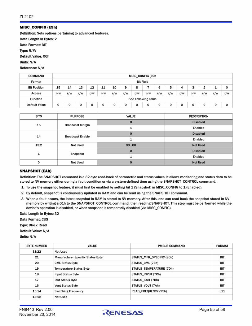
ZL2102
MISC_CONFIG (E9h)Definition: Sets options pertaining to advanced features.
Data Length in Bytes: 2
Data Format: BIT
Type: R/W
Default Value: 00h
Units: N/A
Reference: N/A
SNAPSHOT (EAh)Definition: The SNAPSHOT command is a 32-byte read-back of parametric and status values. It allows monitoring and status data to be stored to NV memory either during a fault condition or via a system-defined time using the SNAPSHOT_CONTROL command.
1. To use the snapshot feature, it must first be enabled by setting bit 1 (Snapshot) in MISC_CONFIG to 1 (Enabled).
2. By default, snapshot is continuously updated in RAM and can be read using the SNAPSHOT command.
3. When a fault occurs, the latest snapshot in RAM is stored to NV memory. After this, one can read back the snapshot stored in NV memory by writing a 01h to the SNAPSHOT_CONTROL command, then reading SNAPSHOT. This step must be performed while the device's operation is disabled, or when snapshot is temporarily disabled (via MISC_CONFIG).
Data Length in Bytes: 32
Data Format: CUS
Type: Block Read
Default Value: N/A
Units: N/A
COMMAND MISC_CONFIG (E9h
Format Bit Field
Bit Position 15 14 13 12 11 10 9 8 7 6 5 4 3 2 1 0
Access r/w r/w r/w r/w r/w r/w r/w r/w r/w r/w r/w r/w r/w r/w r/w r/w
Function See Following Table
Default Value 0 0 0 0 0 0 0 0 0 0 0 0 0 0 0 0
BITS PURPOSE VALUE DESCRIPTION
15 Broadcast Margin0 Disabled
1 Enabled
14 Broadcast Enable0 Disabled
1 Enabled
13:2 Not Used 00...00 Not Used
1 Snapshot0 Disabled
1 Enabled
0 Not Used 0 Not Used
BYTE NUMBER VALUE PMBUS COMMAND FORMAT
31:22 Not Used
21 Manufacturer Specific Status Byte STATUS_MFR_SPECIFIC (80h) BIT
20 CML Status Byte STATUS_CML (7Eh) BIT
19 Temperature Status Byte STATUS_TEMPERATURE (7Dh) BIT
18 Input Status Byte STATUS_INPUT (7Ch) BIT
17 Iout Status Byte STATUS_IOUT (7Bh) BIT
16 Vout Status Byte STATUS_VOUT (7Ah) BIT
15:14 Switching Frequency READ_FREQUENCY (95h) L11
13:12 Not Used
FN8440 Rev 2.00 Page 55 of 58November 20, 2014

ZL2102
BLANK_PARAMS (EBh) Definition: Returns a 16-byte string that indicates which parameter values were either retrieved by the last RESTORE operation or have been written since that time. Reading BLANK_PARAMS immediately after a restore operation allows the user to determine which parameters are stored in that store. A one indicates the parameter is not present in the store and has not been written since the RESTORE operation. This command is used internally to determine if pin strap values should be used. Contact the factory for the BLANK_PARAMS bit-map if needed.
Data Length in Bytes: 16
Data Format: BIT
Type: Block Read
Default Value: FF…FFh
Units: N/A
Reference: N/A
SNAPSHOT_CONTROL (F3h)Definition: Writing a 1h will cause the device to copy the current SNAPSHOT values from NV memory to the 32-byte SNAPSHOT command parameter. Writing a 2h will cause the device to write the current SNAPSHOT values to NV memory. All other values will be ignored. Output must be disabled when writing to NV memory.
Data Length in Bytes: 1
Data Format: BIT
Type: R/W
Default Value: 00h
Units: N/A
RESTORE_FACTORY (F4h)Definition: Restores the device to the hard-coded Default values and pin strap definitions. The device retains the USER store for restoring. Output must be disabled when writing this command.
Data Length in Bytes: 0
Data Format: N/A
Type: Write only
Default Value: N/A
Units: N/A
Reference: N/A
11:10 Internal Temperature READ_TEMPERATURE_1 (8Dh) L11
9:8 Duty Cycle READ_DUTY_CYCLE (94h) L11
7:6 Peak Current N/A L11
5:4 Load Current READ_IOUT (8Ch) L11
3:2 Vout READ_VOUT (8Bh) L16u
1:0 Vin READ_VIN (88h) L11
BYTE NUMBER VALUE PMBUS COMMAND FORMAT
COMMAND SNAPSHOT_CONTROL (F3h)
Format Bit Field
Bit Position 7 6 5 4 3 2 1 0
Access r/w r/w r/w r/w r/w r/w r/w r/w
Function See Following Table
Default Value 0 0 0 0 0 0 0 0
VALUE DESCRIPTION
01h Copy SNAPSHOT values to SNAPSHOT command
02h Copy SNAPSHOT values to NV memory
FN8440 Rev 2.00 Page 56 of 58November 20, 2014

ZL2102
Intersil products are manufactured, assembled and tested utilizing ISO9001 quality systems as notedin the quality certifications found at www.intersil.com/en/support/qualandreliability.html
Intersil products are sold by description only. Intersil may modify the circuit design and/or specifications of products at any time without notice, provided that such modification does not, in Intersil's sole judgment, affect the form, fit or function of the product. Accordingly, the reader is cautioned to verify that datasheets are current before placing orders. Information furnished by Intersil is believed to be accurate and reliable. However, no responsibility is assumed by Intersil or its subsidiaries for its use; nor for any infringements of patents or other rights of third parties which may result from its use. No license is granted by implication or otherwise under any patent or patent rights of Intersil or its subsidiaries.
For information regarding Intersil Corporation and its products, see www.intersil.com
For additional products, see www.intersil.com/en/products.html
© Copyright Intersil Americas LLC 2013-2014. All Rights Reserved.All trademarks and registered trademarks are the property of their respective owners.
About IntersilIntersil Corporation is a leading provider of innovative power management and precision analog solutions. The company's products address some of the largest markets within the industrial and infrastructure, mobile computing and high-end consumer markets.
For the most updated datasheet, application notes, related documentation and related parts, please see the respective product information page found at www.intersil.com.
You may report errors or suggestions for improving this datasheet by visiting www.intersil.com/ask.
Reliability reports are also available from our website at www.intersil.com/support
Revision HistoryThe revision history provided is for informational purposes only and is believed to be accurate, but not warranted. Please go to the web to make sure that you have the latest revision.
DATE REVISION CHANGE
November 20, 2014 FN8440.2 Page 7 - Added note “Compliance to datasheet limits is assured by one or more methods: production test, characterization and/or design.” Reference to this note added to MIN/MAX column headings.
Page 13, replaced Table 7.
Page 19, PMBus Command Summary table, changed VOUT_MARGIN_HIGH and VOUT_MARGIN_LOW data format from L11 to L16u.
Page 26, changed VOUT_MARGIN_HIGH and VOUT_MARGIN_LOW data format from L11 to L16u. Also updated both tables.
Page 40, bit table, bit 9 meaning, changed from "A bit in STATUS_OTHER is set." to "A bit in STATUS_VOUT, STATUS_IOUT,STATUS_MFR_SPECIFIC, or STATUS_VIN is set."
POD correction - changed L36.6x6C to L36.6x6A
August 22, 2013 FN8440.1 Initial Release
FN8440 Rev 2.00 Page 57 of 58November 20, 2014

ZL2102
FN8440 Rev 2.00 Page 58 of 58November 20, 2014
Package Outline Drawing
L36.6x6A36 LEAD QUAD FLAT NO-LEAD PLASTIC PACKAGERev 1, 9/09
located within the zone indicated. The pin #1 indentifier may be
Unless otherwise specified, tolerance : Decimal ± 0.05
Tiebar shown (if present) is a non-functional feature.
The configuration of the pin #1 identifier is optional, but must be
between 0.15mm and 0.30mm from the terminal tip.
Dimension b applies to the metallized terminal and is measured
Dimensions in ( ) for Reference Only.
Dimensioning and tolerancing conform to AMSE Y14.5m-1994.
6.
either a mold or mark feature.
3.
5.
4.
2.
Dimensions are in millimeters.1.
NOTES:
BOTTOM VIEW
DETAIL "X"
SIDE VIEW
TYPICAL RECOMMENDED LAND PATTERN
TOP VIEW
( 4. 10 )
( 5. 60 TYP )
(36X 0.25 )
( 36X 0.80 )
( 36 X 0 . 50 )
0 . 00 MIN.0 . 05 MAX.
0 . 2 REFC
MAX 0.90
5
0.10 C
0.08 C
C
6.0
0
(4X) 0.15
6
PIN 1INDEX AREA
6.00
B
A
4 .10 ± 0.10
36X 0.60 ± 0.10 36X 0.25
C0.10 M A B
4
19
18
9
10
PIN #1
27
28
36X
1
36
0.506
4.04X
INDEX AREA
Compliant to JEDEC MO-220VJJD.7.