© 2012 xiangyu ding - ideals
TRANSCRIPT

© 2012 Xiangyu Ding
OBSERVER BASED FAULT DETECTION FILTERS FOR THREE-PHASE INVERTERS ANDSTATCOMS
BY
XIANGYU DING
THESIS
Submitted in partial fulfillment of the requirementsfor the degree of Master of Science in Electrical and Computer Engineering
in the Graduate College of theUniversity of Illinois at Urbana-Champaign, 2012
Urbana, Illinois
Adviser:
Assistant Professor Alejandro Dominguez-Garcia

ABSTRACT
The introduction of power electronics has brought great benefits in terms of size, weight, per-
formance, and feasibility to various electrical systems. However, with increasing penetration of
power electronics circuits in safety- and mission-critical systems, the reliability of the power elec-
tronics is becoming an issue of increasing concern. To increase the overall reliability of the power
electronic circuit, one key area is developing effective mechanisms for fault detection and isola-
tion. While average models have been proposed for fault detection, these average models disregard
dynamics at switching frequency, which are sometimes crucial in determining the exact health of
power electronic circuit components.
This thesis develops and experimentally demonstrates a class of model-based fault detection
and isolation filters for three-phase AC-DC power electronics systems that is able to detect all
possible component faults, offers fast detection, and has the ability to capture slow degradation in
individual components. The structure of these filters is similar to that of a piecewise linear ob-
server, and in the absence of faults, the filter error residual converges to zero. On the other hand,
whenever a fault occurs, by appropriately choosing the filter gain, the filter error residual will
exhibit certain geometric characteristics that allow the fault to be detected and, in certain cases,
also isolated. While the theory developed is general, the analysis, simulations, and experimen-
tal demonstration are focused on systems implementing three-phase AC-DC converters used, for
example, in drive applications and distributed static compensators.
ii

To my parents, for their love and support; and to my adviser, for guiding me along this research
project
iii

ACKNOWLEDGMENTS
I would like to thank my adviser Professor Alejandro Domínguez-García for helping me revise my
mathematical derivations and explaining to me the key theory behind this research, and for helping
me revise my paper and teaching me so much about technical writing. I want to thank our lab
manager Kevin Colravy and fellow graduate student Jarod Delhotal for their help in building the
modular inverter, and other graduate students who are part of the power and energy group at UIUC
for answering many of my questions. I would also like to thank Jason Poon and Ivan Celanovic
from MIT for their help with setting up the HIL 400 system. They built a quite impressive piece
of hardware and I’m very thankful to them for introducing it to our group.
iv
CONTENTS
LIST OF TABLES . . . . . . . . . . . . . . . . . . . . . . . . . . . . . . . . . . . . . . . vii
LIST OF FIGURES . . . . . . . . . . . . . . . . . . . . . . . . . . . . . . . . . . . . . . . viii
Chapter 1 INTRODUCTION . . . . . . . . . . . . . . . . . . . . . . . . . . . . . . . . . 11.1 Background on Fault Detection for the Six-pulse Circuit . . . . . . . . . . . . . . 21.2 Piecewise-linear FDI Filter . . . . . . . . . . . . . . . . . . . . . . . . . . . . . . 41.3 Thesis Organization . . . . . . . . . . . . . . . . . . . . . . . . . . . . . . . . . . 5
Chapter 2 MODELING FRAMEWORK . . . . . . . . . . . . . . . . . . . . . . . . . . . 62.1 Nominal (Pre-Fault) System Model . . . . . . . . . . . . . . . . . . . . . . . . . . 62.2 Post-Fault System Model . . . . . . . . . . . . . . . . . . . . . . . . . . . . . . . 9
Chapter 3 FAULT DETECTION AND ISOLATION FILTER DESIGN . . . . . . . . . . . 113.1 The FDI Filter Design Problem . . . . . . . . . . . . . . . . . . . . . . . . . . . . 123.2 Solution to the FDI Filter Design Problem . . . . . . . . . . . . . . . . . . . . . . 13
Chapter 4 DESIGN AND ANALYSIS OF A FDI FILTER FOR A THREE-PHASEINVERTER WITH RL LOAD SYSTEM . . . . . . . . . . . . . . . . . . . . . . . . . . 184.1 Fault Detection and Isolation Filter . . . . . . . . . . . . . . . . . . . . . . . . . . 184.2 Analytical and Simulation Results . . . . . . . . . . . . . . . . . . . . . . . . . . 194.3 Experimental Results . . . . . . . . . . . . . . . . . . . . . . . . . . . . . . . . . 26
Chapter 5 DESIGN AND ANALYSIS OF A FDI FILTER FOR A D-STATCOM . . . . . 315.1 Pre-Fault Dynamics and FDI Filter . . . . . . . . . . . . . . . . . . . . . . . . . . 325.2 Analytical and Simulation Results . . . . . . . . . . . . . . . . . . . . . . . . . . 345.3 Real-Time Simulation Results . . . . . . . . . . . . . . . . . . . . . . . . . . . . 37
Chapter 6 IMPLEMENTATION CONSTRAINTS . . . . . . . . . . . . . . . . . . . . . . 406.1 Noise and Delay Modeling . . . . . . . . . . . . . . . . . . . . . . . . . . . . . . 406.2 Parameter Estimation and Sensitivity Analysis . . . . . . . . . . . . . . . . . . . . 42
Chapter 7 CONCLUSIONS . . . . . . . . . . . . . . . . . . . . . . . . . . . . . . . . . . 44
REFERENCES . . . . . . . . . . . . . . . . . . . . . . . . . . . . . . . . . . . . . . . . . 45
v

Appendix A M-CODE FOR FAULT DYNAMIC DERIVATION . . . . . . . . . . . . . . 48A.1 Change of Inductance Fault . . . . . . . . . . . . . . . . . . . . . . . . . . . . . . 48A.2 Change of Capacitance Fault . . . . . . . . . . . . . . . . . . . . . . . . . . . . . 52A.3 Switch 1 Open Circuit Fault . . . . . . . . . . . . . . . . . . . . . . . . . . . . . 56
Appendix B SIMULATION MODELS . . . . . . . . . . . . . . . . . . . . . . . . . . . . 61B.1 RL Load Inverter Simulation Model . . . . . . . . . . . . . . . . . . . . . . . . . 61B.2 D-STATCOM Simulation Model . . . . . . . . . . . . . . . . . . . . . . . . . . . 62
vi

LIST OF TABLES
2.1 Possible Open/Close Switch Positions . . . . . . . . . . . . . . . . . . . . . . . . 6
4.1 Inverter with RL load: Model parameters . . . . . . . . . . . . . . . . . . . . . . 194.2 Inverter with RL load: Fault magnitude function and signature for faults caus-
ing changes in phase resistance. . . . . . . . . . . . . . . . . . . . . . . . . . . . 204.3 Inverter with RL load: Fault magnitude function and signature for faults caus-
ing changes in phase inductance. . . . . . . . . . . . . . . . . . . . . . . . . . . . 234.4 Inverter with RL load: Fault magnitude function and signature for faults in
current sensors. . . . . . . . . . . . . . . . . . . . . . . . . . . . . . . . . . . . . 26
5.1 D-STATCOM model parameters . . . . . . . . . . . . . . . . . . . . . . . . . . . 345.2 D-STATCOM: Fault magnitude function and signature for faults in DC link
capacitor. . . . . . . . . . . . . . . . . . . . . . . . . . . . . . . . . . . . . . . . 365.3 D-STATCOM: Fault magnitude function and signature for switch open-circuit
faults. . . . . . . . . . . . . . . . . . . . . . . . . . . . . . . . . . . . . . . . . . 37
vii
LIST OF FIGURES
2.1 Inverter with RL load system. . . . . . . . . . . . . . . . . . . . . . . . . . . . . . 7
4.1 Inverter with RL load: Simulation of filter response for a fault causing phase cresistance to decrease by 5 Ω. . . . . . . . . . . . . . . . . . . . . . . . . . . . . . 20
4.2 Inverter with RL load: Simulation of filter response for an open-circuit fault inphase c. . . . . . . . . . . . . . . . . . . . . . . . . . . . . . . . . . . . . . . . . 22
4.3 Inverter with RL load: Simulation of filter response for a fault causing phase cinductance to decrease by −5 mH. . . . . . . . . . . . . . . . . . . . . . . . . . . 22
4.4 Inverter with RL load: Simulation of filter response for a fault causing SW5 toalways stay open. . . . . . . . . . . . . . . . . . . . . . . . . . . . . . . . . . . . 24
4.5 Inverter with RL load: Frequency analysis of the filter residual response forfaults phase in c. . . . . . . . . . . . . . . . . . . . . . . . . . . . . . . . . . . . 24
4.6 Inverter with RL load: Simulation of filter response for an omission fault inphase c current sensor. . . . . . . . . . . . . . . . . . . . . . . . . . . . . . . . . 26
4.7 Functional diagram of the experimental setup. . . . . . . . . . . . . . . . . . . . 264.8 Diagram of actual experimental setup. . . . . . . . . . . . . . . . . . . . . . . . . 274.9 Inverter with RL load: Experimental filter response for an phase c open circuit fault. 294.10 Inverter with RL load: Experimental filter response for an omission fault in
phase c current sensor. . . . . . . . . . . . . . . . . . . . . . . . . . . . . . . . . 30
5.1 D-STATCOM simulation block diagram. . . . . . . . . . . . . . . . . . . . . . . . 315.2 D-STATCOM: Simulation of filter response for 50% decrease in DC link ca-
pacitance. . . . . . . . . . . . . . . . . . . . . . . . . . . . . . . . . . . . . . . . 345.3 D-STATCOM: Simulation of filter response for a fault causing phase c resis-
tance to change from 0.1 Ω to 0.5 Ω. . . . . . . . . . . . . . . . . . . . . . . . . 365.4 D-STATCOM setup with simulated plant. . . . . . . . . . . . . . . . . . . . . . . 385.5 D-STATCOM HIL400 real-time simulation results. . . . . . . . . . . . . . . . . . 38
6.1 RMS filter residual vs sampling frequency. . . . . . . . . . . . . . . . . . . . . . . 416.2 RMS filter residual vs sensor delay. . . . . . . . . . . . . . . . . . . . . . . . . . 416.3 Parameter sensitivity simulation results: (a) resistance vs inductance, (b) resis-
tance vs capacitance, and (c) inductance vs capacitance. . . . . . . . . . . . . . . . 43
B.1 Inverter with RL load and fault detection filter Simulink model . . . . . . . . . . . 61B.2 D-STATCOM with fault detection filter Simulink model . . . . . . . . . . . . . . 62
viii
Chapter 1
INTRODUCTION
Reliability of power electronics systems is of great importance in may safety- and mission-critical
applications, such as aerospace systems, and for voltage and power flow control in power grids
(commonly referred to as FACTs). In general, in any engineered system, ensuring a high level of
reliability is usually achieved by including fault tolerance into the system design. With respect to
this, there are three key elements to any fault-tolerant system design: i) component redundancy, ii)
fault detection and isolation (FDI) system, and iii) a reconfiguration system that, once a fault has
been detected and isolated, substitutes the faulty component by a redundant one, or reconfigures
the control to compensate for the fault. In this research, we focus on a new approach to FDI system
design for power electronics applications, with special emphasis on the class of systems that im-
plement the two-level three-phase converters, e.g., inverters for variable-speed drive applications,
active filters, and Distributed Static Compensators (D-STATCOMs).
Any FDI system executes three tasks [1]: i) detection, makes a binary decision whether or
not a fault has occurred, ii) isolation, determines the location of the faulty component, and iii) a
severity assessment, determines the extent of the fault. In general, methods for FDI in electrical
systems can be broadly classified into three different categories: i) model-based, uses knowledge
of fault models to design residual generators that can point to specific faults [2, 3]; ii) artificial
intelligence, uses neural networks and fuzzy logic to develop expert systems that once trained can
point to specific faults [4]; and iii) empirical and signal processing, use spectral analysis to identify
specific signatures of a certain fault [5].
1

1.1 Background on Fault Detection for the Six-pulse Circuit
The two-level inverter (six-pulse) circuit is one of the most widely used power electronic circuits
for three-phase rectification or inversion. Its application ranges from inverters systems, motor
drives to High Voltage Direct Current (HVDC) systems and Flexible AC Transmission Systems
(FACTS).
The most widely used application of the two-level inverter are in three-phase inverters that take
in a fixed DC source and generates three-phase AC. These inverters are used in interconnecting
renewable resources like solar and wind to the grid, and in drives of induction, permanent magnet
and synchronous motors in cars, ships, aircrafts, and factories. With these inverters powering much
of the basic infrastructure of the modern world, it is very important to ensure their reliability.
Another application of the two-level inverter is in static compensator systems. The STATCOM
is a power system controller for reactive power compensation [6]. In high-power level transmis-
sion network applications, multi-level (or multi-pulse) converter topologies are often utilized to
achieve higher rating and to reduce harmonic injection [7]. However, increasing the number of
levels (or pulses) also increases system complexity and the likelihood of device failure [8]. On the
distribution level, the D-STATCOM is a lower-voltage controller that is often tied to highly non-
linear loads to reduce their disturbance to the grid or to custom power loads that require very strict
power quality control [9, 10]. The most basic D-STATCOM system consists of a six-pulse circuit
with the DC end tied to a DC capacitor and the AC side connected in shunt to the power distribu-
tion network through a coupling transformer. The switches are usually operated by a PWM-based
control schemes with switching frequencies in the several kHz range. Depending on the control
algorithm, the D-STATCOM system can be used for voltage regulation, power factor correction, or
for elimination of harmonic distortion, but the exact operating scheme is determined by the specific
application. Based on [9], several large industrial users have experienced large financial losses as
a result of even minor lapses in the quality of electricity supply, so the reliability of D-STATCOMs
is very important to these industries.
Most of the work done on fault detection in six-pulse based systems is in the area of motor
drives systems. The most common method of handling reliability is through redundancy and using
protective mechanisms like fuses and breaks. A good demonstration of this approach can be found
2

in [11], where a fault tolerant six-pulse voltage source inverter (VSI) was proposed which uses an
additional fourth phase to isolate open circuit faults and fuses on each switch to isolate short circuit
faults. While this approach can improve reliability, it also significantly increases overall cost of
the system and increases the number of component counts. While the overall reliability of the
system might improve, the likelihood for individual component failure is significantly increased.
Another fault detection method based on various system voltage measurements was proposed in
[12]. For this study, they relied on the fact that the phase and neutral voltages can be accurately
estimated using the PWM reference signals. By comparing the measured inverter pole voltage,
phase voltage, line voltage, or neutral voltage with the expected voltage references obtained from
the PWM reference signals, it is possible to detect open and short circuit faults of the switches.
Their study covered almost all possible combinations of open and short circuit faults that can
happen in a two-level inverter, but there was still a number of issues that were not addressed. In
order to implement such a detection method, additional voltage sensors were needed. The addition
of these new voltage sensors increases the likelihood of sensor-related faults into the system and
the method does not have any built-in ways of dealing with sensor faults. In [13], two model-based
FDI algorithms were proposed, one based on current-vector trajectories in the alpha-beta reference
frame, and the other based on the instantaneous frequency of the current vector. In this study, they
calculate the instantaneous current in the alph-beta reference frame. Under un-faulted conditions,
the current follows a well-defined trajectory. After a fault happens, the trajectories of the current
changes, which allows the fault to be detected. These algorithms were proven to be effective for
switch open circuit faults, but other types of failures were not considered.
Aside from the methods proposed for six-pulse based circuits, other FDI methods have also
been proposed for more general STATCOM systems. For example, in [8], faults were detected by
comparing the DC link voltages with the expected voltage found based on the current switching
signal. In [14], the harmonic signatures generated by different types of faults are used for FDI.
There is also work on the application of neural network fault diagnosis for multi-level voltage
source inverters [15].
3
1.2 Piecewise-linear FDI Filter
In this research, we propose the use of piecewise-linear observers for designing fault detection
filters, using the three-phase two-level inverter circuit as a demonstrating example. In absence of
faults, the detection filter asymptotically converges to the state variable actual values. When a
fault occurs, the estimated values diverge from the state variable actual values. The filter resid-
ual, defined as the difference between the actual system output and the filter output, accurately
determines the location and extent of the fault. The reason for using piecewise-linear observers for
designing fault detection filter is as follows. Most of the fault detection approaches discussed in
the previous section are focused on system characteristics that only allow detection and isolation
of some particular types of faults in the system. In order to capture all possible component faults
and degradations in the system, a full model of the power electronics circuit is needed. While
average models have been proposed to allow linearized analysis of the power electronic systems
in most cases, these average models cannot properly capture the effect of a fault on the system
dynamics, and thus cannot be used to design observer-based fault detection filters. This can be
easily illustrated with a fault that causes changes in capacitance which lead to increased ripple.
While this increased ripple could degrade system performance, it does not manifest in the average
model. A piecewise-linear model, on the other hand, is able to capture such effects.
A piecewise-linear FDI filter is comprised of a collection of linear state-space models (sub-
systems), each of which has the same structure of a Luenberger observer ([16, 17]), including the
corresponding gain matrix. The transitions between the subsystems are determined by the same
rules that govern the switching in the actual system—a challenge is to provide a real-time com-
putational platform that can execute the FDI filter at high-enough speed. Another challenge is to
design the individual gain matrices so that i) the detection filter residual exhibits certain geometric
characteristics for each particular fault, and ii) the observer is stable. With respect to ii), it is well-
known that choosing the individual gains such that each subsystem is stable is not sufficient for
ensuring stability (see, e.g., [18]). Thus, as part of the FDI filter design procedure outlined in this
thesis, we provide sufficient conditions that ensure the choice of gain matrices renders the filter
stable.
In order to illustrate the design procedure and the performance of the resulting filters, we
4
provide two simulation-based case studies that involve a three-phase two-level inverter and a D-
STATCOM. In addition, we experimentally demonstrate the feasibility of the proposed filters for
detecting and isolating faults in a system comprised of a three-phase two-level inverter connected
in one end to a voltage source and to a three-phase balanced load in the other. In this regard, in
order to realize a FDI filter for such a setting, it is necessary to run, in real time, a copy of the
linear-switched state-space model that describes the actual system, including the switching among
the subsystems at frequencies that range from hundreds to thousands of Hz depending on the appli-
cation. In order to achieve this, we rely on an application-specific processor architecture, tailored
for low-latency execution of piecewise-linear hybrid systems [19, 20]. This computational plat-
form enables the simulation of linear-switched state-space models for power electronics converters
with a fixed 1 µs simulation time step, including input-output latency. This application-specific
architecture guarantees the computation for each time step to be shorter than the fixed simulation
time step.
1.3 Thesis Organization
The remainder of this thesis is organized as follows. Chapter 2 introduces the modeling framework.
Chapter 3 formulates and provides a solution to the FDI filter design problem. Chapter 4 develops
and demonstrates a FDI filter for a three-phase inverter connected to an RL load. In Chapter
5, we design a FDI filter for a D-STATCOM. Chapter 6 discusses implementation constraints.
Concluding remarks are presented in Chapter 7.
5

Chapter 2
MODELING FRAMEWORK
In this chapter, we develop the linear-switched system modeling framework adopted throughout
the thesis and introduce relevant notation and terminology used in the remainder of the paper.
Throughout the chapter, we use the system in Fig. 2.1 to introduce basic ideas, although the
framework is general to a large class of linear-switched systems.
2.1 Nominal (Pre-Fault) System Model
Consider the system in Fig. 2.1, comprised of a voltage source Vdc, a three-phase inverter and
an RL load. This system can be modeled as a switched system1. A switched system can be
described by a collection of state-space models—referred to as subsystems or modes—together
with a switching signal,2 the role of which is to specify, at each time instant, the active mode [18].
In the system of Fig. 2.1, each mode can be obtained by applying Kirchhoff’s laws to each of the
circuits that results from the possible open/closed switch combinations. The switching signal is
defined by the specifics of the control system that determines the switch open/close positions.
Table 2.1: Possible Open/Close Switch Positions
p 1 2 3 4 5 6 7 8s1/s2 0 0 0 0 1 1 1 1s3/s4 0 0 1 1 0 0 1 1s5/s6 0 1 0 1 0 1 0 1
1A dynamical system that can described by the interaction of some continuous and discrete dynamic behavior isreferred to as hybrid system. A switched system is a continuous-time system with (isolated) discrete switching events.A switched system can be obtained from a hybrid system by neglecting the details of the discrete behavior [18].
2A switching signal is a piecewise constant function with a finite number of discontinuities—the switching times—on every bounded time interval, taking a constant value on every interval between two consecutive switching times.
6

SW1
SW2
SW3
SW4
SW5
SW6
La
Lb
Lc
Ra
Rb
Rc
ia(t)
ib(t)
ic(t)
Vdc
Figure 2.1: Inverter with RL load system.
For the system of Fig. 2.1, there are six switches, which means there are 64 possible combi-
nations; however, in normal operation, we have that, on each phase, there is exactly one switch
closed at any given time, which results in only eight feasible modes. Let P = 1,2, . . . ,8 be the
set indexing the feasible system modes, and let si(t), i = 1,2, . . . ,6, denote an indicator variable
that, at time t, takes value 0 whenever switch i (denoted by SWi), and 1 whenever is closed. Then,
each p ∈P is uniquely defined by an open/closed switch combination s1(t), s2(t), . . . ,s6(t)
as defined in Table 2.1. Therefore, the active mode at time t can be indicated by a function
σ : [0,∞)→P (the switching signal) and the system dynamics can be compactly described by a
linear-switched state-space model of the form
Eσ(t)dx(t)
dt= Fσ(t)x(t)+Gσ(t)v(t), (2.1)
7
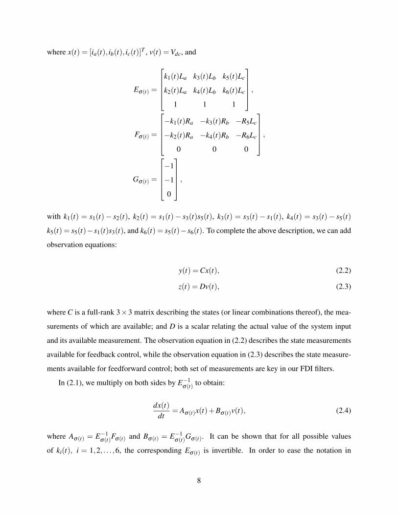
where x(t) = [ia(t), ib(t), ic(t)]T , v(t) =Vdc, and
Eσ(t) =
k1(t)La k3(t)Lb k5(t)Lc
k2(t)La k4(t)Lb k6(t)Lc
1 1 1
,
Fσ(t) =
−k1(t)Ra −k3(t)Rb −R5Lc
−k2(t)Ra −k4(t)Rb −R6Lc
0 0 0
,
Gσ(t) =
−1
−1
0
,
with k1(t) = s1(t)− s2(t), k2(t) = s1(t)− s3(t)s5(t), k3(t) = s3(t)− s1(t), k4(t) = s3(t)− s5(t)
k5(t) = s5(t)− s1(t)s3(t), and k6(t) = s5(t)− s6(t). To complete the above description, we can add
observation equations:
y(t) =Cx(t), (2.2)
z(t) = Dv(t), (2.3)
where C is a full-rank 3×3 matrix describing the states (or linear combinations thereof), the mea-
surements of which are available; and D is a scalar relating the actual value of the system input
and its available measurement. The observation equation in (2.2) describes the state measurements
available for feedback control, while the observation equation in (2.3) describes the state measure-
ments available for feedforward control; both set of measurements are key in our FDI filters.
In (2.1), we multiply on both sides by E−1σ(t) to obtain:
dx(t)dt
= Aσ(t)x(t)+Bσ(t)v(t), (2.4)
where Aσ(t) = E−1σ(t)Fσ(t) and Bσ(t) = E−1
σ(t)Gσ(t). It can be shown that for all possible values
of ki(t), i = 1,2, . . . ,6, the corresponding Eσ(t) is invertible. In order to ease the notation in
8
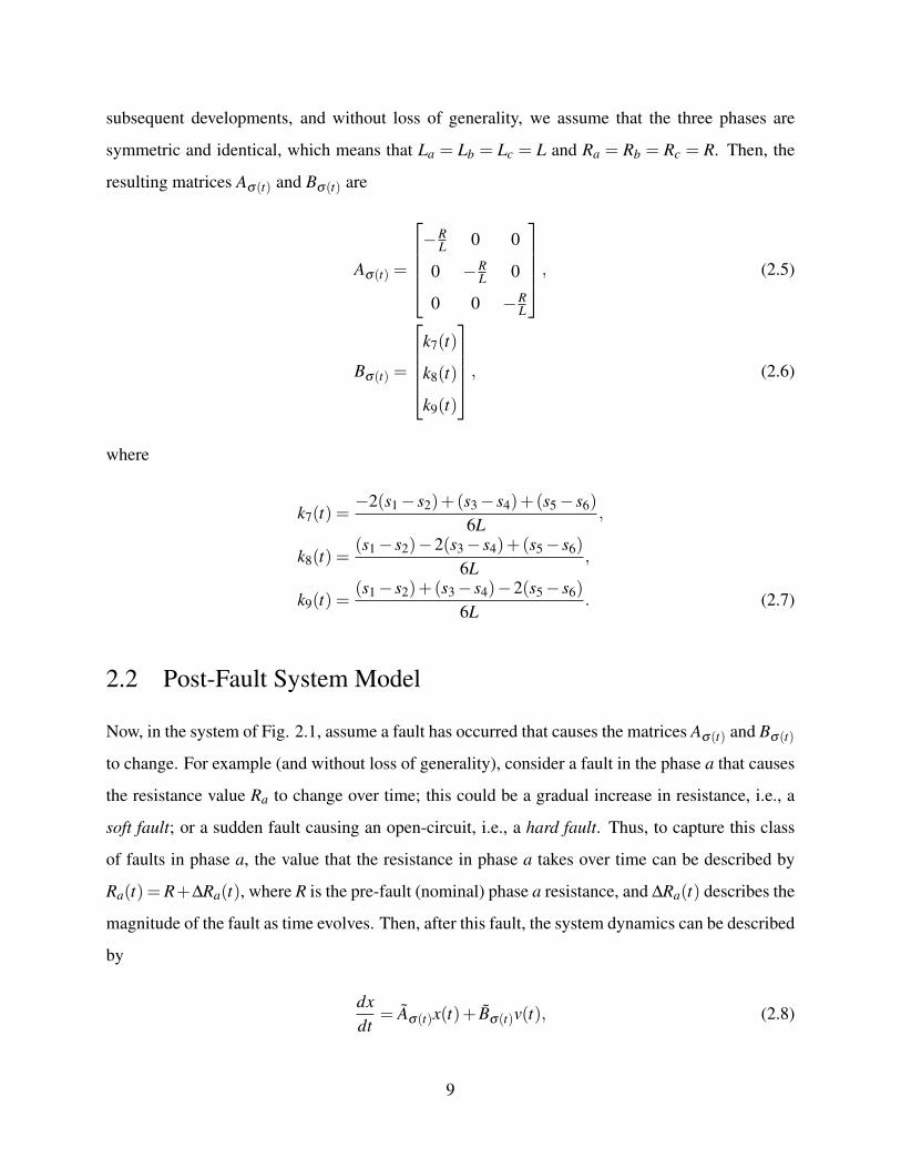
subsequent developments, and without loss of generality, we assume that the three phases are
symmetric and identical, which means that La = Lb = Lc = L and Ra = Rb = Rc = R. Then, the
resulting matrices Aσ(t) and Bσ(t) are
Aσ(t) =
−R
L 0 0
0 −RL 0
0 0 −RL
, (2.5)
Bσ(t) =
k7(t)
k8(t)
k9(t)
, (2.6)
where
k7(t) =−2(s1− s2)+(s3− s4)+(s5− s6)
6L,
k8(t) =(s1− s2)−2(s3− s4)+(s5− s6)
6L,
k9(t) =(s1− s2)+(s3− s4)−2(s5− s6)
6L. (2.7)
2.2 Post-Fault System Model
Now, in the system of Fig. 2.1, assume a fault has occurred that causes the matrices Aσ(t) and Bσ(t)
to change. For example (and without loss of generality), consider a fault in the phase a that causes
the resistance value Ra to change over time; this could be a gradual increase in resistance, i.e., a
soft fault; or a sudden fault causing an open-circuit, i.e., a hard fault. Thus, to capture this class
of faults in phase a, the value that the resistance in phase a takes over time can be described by
Ra(t) = R+∆Ra(t), where R is the pre-fault (nominal) phase a resistance, and ∆Ra(t) describes the
magnitude of the fault as time evolves. Then, after this fault, the system dynamics can be described
by
dxdt
= Aσ(t)x(t)+ Bσ(t)v(t), (2.8)
9

where Bσ(t) = Bσ(t), ∀t, and
Aσ(t) =
−R
L −2∆Ra(t)
3L 0 0∆Ra(t)
3L −RL 0
∆Ra(t)3L 0 −R
L
.
It can be shown (see, e.g., [21]) that (2.8) can be written as the pre-fault (nominal) dynamics in
(2.1) plus an additional term that captures the effect of the fault on the pre-fault system dynamics:
dx(t)dt
= Aσ(t)x+Bσ(t)v(t)+φ(t) f , (2.9)
where f = [−2,1,1]T is referred to as the fault signature, and φ(t) = ∆Ra(t)3L ia(t) is referred to as
the fault magnitude function. In this case, although the fault magnitude is not a function of the
switching signal, in general it is; this becomes apparent in the case studies presented in chapters 4
and 5.
A similar development follows for the case when there is a fault that affects the observation
equation in (2.2)–(2.3), i.e., we can write the post-fault observation equation as the pre-fault ob-
servation equation plus an additional term that captures the effect of the fault. Thus
y(t) =Cx(t)+θ(t)g, (2.10)
z(t) = Dv(t)+ρ(t)h, (2.11)
where θ(t)g and ρ(t)h capture the effect of faults.
10

Chapter 3
FAULT DETECTION AND ISOLATION FILTERDESIGN
In this chapter, we generalize the problem setting described in chapter 2 by considering s different
possible component faults, the jth of which is described by a real-valued function φ j(t)—the fault
magnitude function—and a vector f j—the fault signature. Similarly, we also assume that the state-
measurement (input-measurement) sensors are subject to r (q) faults, each of which is captured by
an additive perturbation of the form θ j(t)g j (ρ j(t)h j), where θ j(t) (ρ j(t)) is the fault magnitude
function and g j (h j) is the fault signature. As before, we restrict ourselves to the class of power
electronics systems that can be described by a linear-switched state-space model.
Let x(t)∈Rn denote the system state variables, v(t)∈Rm the inputs, y(t)∈Rn the observations,
and σ(t) the switching signal. Then, the dynamics of any system within this class (including the
behavior in the presence of faults) can be generally described by
dx(t)dt
= Aσ(t)x(t)+Bσ(t)v(t)+s
∑j=1
φ j(t) f j,
y(t) =Cx(t)+r
∑j=1
θ j(t)g j,
z(t) = Dv(t)+q
∑j=1
ρ j(t)h j. (3.1)
We additionally impose that the matrix C ∈Rn×n is full rank, i.e., respectively, all the states (or lin-
ear combinations thereof) can be measured. This automatically ensures that the pairs Ap,C, p ∈
P , are observable, which is necessary in the development of our detection filters. Additionally,
we also impose that D ∈ Rm×m is full rank. The assumption that measurements of all the states
(and inputs), or linear combinations of them, are available is not very restrictive as those are in
most cases available as they are needed, in general, for control.
11
3.1 The FDI Filter Design Problem
Consider the linear-switched system in (3.1); the objective is to design a causal filter that takes
z(t), y(t), and σ(t) as inputs and generates a residual γ(t) with the following properties:
P1 Whenever the system is fault-free, i.e., for all t > 0, φi(t) fi = 0, ∀i, θ j(t)g j = 0, ∀ j, and
ρl(t)hl =,0, ∀l, then the filter residual asymptotically converges to zero, i.e., limt→∞ γ(t) =
0.
P2 When a fault occurs at time t = t f affecting Aσ(t),Bσ(t), i.e., for some j, φ j(t) f j 6= 0, ∀t ≥
t f , then as t→ ∞, the filter residual tends to align with the vector C fi.
P3 When a fault occurs at time t = t f affecting C, i.e., for some j, θ j(t)g j 6= 0, ∀t > t f , then as
t→ ∞, the filter residual lies in a subspace spanned by C(Ap +µI)g j, p ∈P .
P4 When a fault occurs at time t = t f affecting D, i.e., for some j, ρ j(t)h j 6= 0, ∀t > t f , then as
t→ ∞, the filter residual lies in a subspace spanned by CBpD−1h j, p ∈P .
Next we relate the notions of fault detection and fault isolation to the filter residual desired prop-
erties P1–P4.
Fault detection
This is a binary decision on whether or not a fault has occurred. In this regard, it is clear from
P1-P4 that by directly observing the filter residual, fault detection is straightforward, i.e., if for
large enough t, we have that γ(t)→ 0, then the system is declared fault-free; on the other hand, we
can conclude that a fault affecting a component within the system has occurred if, for all t greater
than some time t f (denoting the time at which the fault occurs), we have that γ(t) 6= 0.
Fault isolation
Once a fault has been detected, fault isolation entails determining the location of the component
where the fault originated. A key observation that can be inferred from P1-P4 is that, if each
fault has a unique signature, it is in general possible to isolate a fault by direct observation of the
12

filter residual direction. On the other hand, if there are two faults with the same signature, by just
inspecting the filter residual direction we cannot distinguish them apart; in this case, the residual
magnitude frequency spectrum provides additional information that can be used for isolation.
3.2 Solution to the FDI Filter Design Problem
In order to solve the FDI filter design problem, we propose a causal filter of the form
dx(t)dt
= Aσ(t)x+Bσ(t)D−1z(t)+Lσ(t)γ(t),
γ(t) = y(t)−Cx(t). (3.2)
where σ(t), Aσ(t), Bσ(t), p ∈P and C as in (3.1); and
Lσ(t) = [µIn +Aσ (t)]C−1, ∀t, (3.3)
for some µ > 0 (In denotes the n× n identity matrix). Next, we establish that with the choice of
Lσ(t)’s in (3.3), the FDI filter in (3.2) satisfies properties P1–P4.
3.2.1 Residual dynamics in the absence of faults
In this case, for all t > 0, in (3.1) we have that φ j(t) f j = 0, ∀ j. Let e(t) := x(t)− x(t), then by
subtracting (3.2) from (3.1), we obtain that
de(t)dt
=[A−Lσ(t)C
]e(t),
but with the choice of Lp in (3.3), we have that
de(t)dt
=−µe(t),
γ(t) =Ce(t),
for some µ > 0, from where we obtain that limt→∞ γ(t) = 0, thus property P1 is satisfied.
13

3.2.2 Residual dynamics for faults affecting Aσ (t),Bσ (t)
In this case, we assume that for some t = t f , the jth fault affecting Ap and/or Bp manifests, i.e.,
φ j(t) f j 6= 0, ∀t ≥ t f . By subtracting (3.2) from (3.1), we obtain that
de(t)dt
=−µe(t)+φ j(t) f j, (3.4)
γ(t) =Ce(t),
thus,
γ(t) =Ce−µte(0)+α j(t)C f j, (3.5)
with
α j(t) =
tˆ
0
e−µ(t−τ)φ j(τ)dτ.
Now, since α j(t) is a scalar and the first term on the right-hand side of (3.5) vanishes as t→ ∞, it
follows that, as t→ ∞, the filter residual γ(t) will align with C f j, thus property P2 is satisfied.
3.2.3 Residual dynamics for faults affecting C
In this case, for some t = t f , the jth affecting C manifests, i.e., θ j(t)g j, ∀t ≥ t f . By subtracting
(3.2) from (3.1), we obtain that
de(t)dt
=−µe(t)−θ j(t)(Aσ(t)+µI)g j, (3.6)
γ(t) =Ce(t).
Let tk, k = 1,2, . . . ,n, with t1 ≥ 0 and tn ≤ t, be the sequence of switching instants in [0, t), then
γ(t) =Ce−µte(0)+n
∑i=0
β j(ti)C(Aσ(ti)+µI)g j, (3.7)
14
where
β j(ti) =−ˆ ti+1
tie−µ(t−τ)
θ j(t)dτ,
with t0 = 0 and tn+1 = t. Let tkp denote a subsequence of tk that corresponds to the time
instants when mode p ∈P is activated. Then, the summation term in (3.7) can be rearranged,
resulting in
γ(t) =Ce−µte(0)+ ∑p∈P
∑l∈tkp
β j(l)C(Ap +µI)g j, (3.8)
Now, since the β j(l)’s are scalars and the first term on the right-hand side of (3.7) vanishes as
t → ∞, it follows that, as t → ∞, the filter residual γ(t) will be a linear combination of C(Ap +
µI)g, p ∈P; thus property P3 is satisfied.
3.2.4 Residual dynamics for faults affecting D
In this case, for some t = t f , the jth affecting D manifests, i.e., ρ j(t)h j, ∀t ≥ t f . By subtracting
(3.2) from (3.1), we obtain
de(t)dt
=−µe(t)−ρ j(t)Bσ(t)D−1h j, (3.9)
γ(t) =Ce(t).
The subsequent development is similar to the one in (3.7)–(3.8), resulting in
γ(t) =Ce−µte(0)+n
∑i=0
κ j(ti)Bσ(t)D−1h j,
with
κ j(ti) =−ˆ ti+1
tie−µ(t−τ)
ρ j(t)dτ,
15

and where tk, k = 1,2, . . . ,n, with t1 ≥ 0 and tn ≤ t, is the sequence of switching instants in [0, t).
Then,
γ(t) =Ce−µte(0)+ ∑p∈P
∑l∈tkp
κ j(l)CBpD−1h j, (3.10)
where tkp is the subsequence of tk that corresponds to the time instants when mode p ∈P
is activated. As before, since the κ j(l)’s are scalars, it follows that, as t → ∞, the first term on
the right-hand side of (3.10) vanishes, and thus γ(t) will be a linear combination of the vectors in
CBpD−1, p ∈P , and therefore property P4 is satisfied.
3.2.5 Fault detection filter frequency response
From (3.4),(3.6), and (3.9), the filter residual dynamics can be expressed as
de(t)dt
+µe(t) = φ j(t) f j +θ j(t)(Aσ(t)+µI)g j +ρ j(t)Bσ(t)D−1h j,
γ(t) =Ce(t).
In the expression for the fault magnitude function shown above, the terms Aσ(t) and Bσ(t) are
time dependent, so deriving a frequency domain expression is not possible. However, in some
symmetric circuits, the terms Aσ(t) and Bσ(t) turn out to be constants. In such cases, these three
fault magnitude functions can be expressed in the frequency domain as
(s+µ)E(s) = φ j(s) f j +θ j(s)(Aσ +µI)g j +ρ j(s)Bσ D−1h j
γ(s) =CE(s).
where E(s), φ j(s),θ j(s), and ρ j(s) are the Laplace transform of e(t), φσ (t), θ j(t), and ρ j(t). Solv-
ing for E(s) results in
E(s) =φ j(s) f j +θ j(s)(Aσ +µI)g j +ρ j(s)Bσ D−1h j
(s+µ), (3.11)
γ(s) =CE(s).
16

Equation 3.11 offers a very compact way to express the fault dynamics and give some important
insight into the fault dynamics. However, it does not capture transient behaviors, which are more
dominant during fast fault transients. For this reason, both time domain and frequency domain
analysis are needed for accurate analysis.
17
Chapter 4
DESIGN AND ANALYSIS OF A FDI FILTER FOR ATHREE-PHASE INVERTER WITH RL LOAD
SYSTEM
In this chapter, we develop FDI filters for the three-phase inverter and RL load system of Fig 2.1.
We first provide analytical expressions for all component fault signatures and associated fault-
magnitude functions, and, for certain faults, we also provide analytical expressions for the filter
residual dynamics. We demonstrate the performance of the FDI filters in both a simulation envi-
ronment and in an experimental setting.
4.1 Fault Detection and Isolation Filter
Consider again the three-phase inverter with RL load of Fig. 2.1, and, as before, assume that the
three phases are symmetric, i.e., La = Lb = Lc = L and Ra = Rb = Rc = R. Then, the nominal (pre-
fault) system dynamics is described by the linear-switched state-space model as in (2.2)–(2.4).
Assume that all the system states and inputs are directly measurable, i.e., C = I3 in (2.2), and
D = I1 in (2.3). Then following the notation in (3.2) and (3.3), a FDI filter for this system is given
by
dx(t)dt
= Aσ(t)x+Bσ(t)z(t)+Lσ(t)γ(t),
γ(t) = y(t)− x(t). (4.1)
18
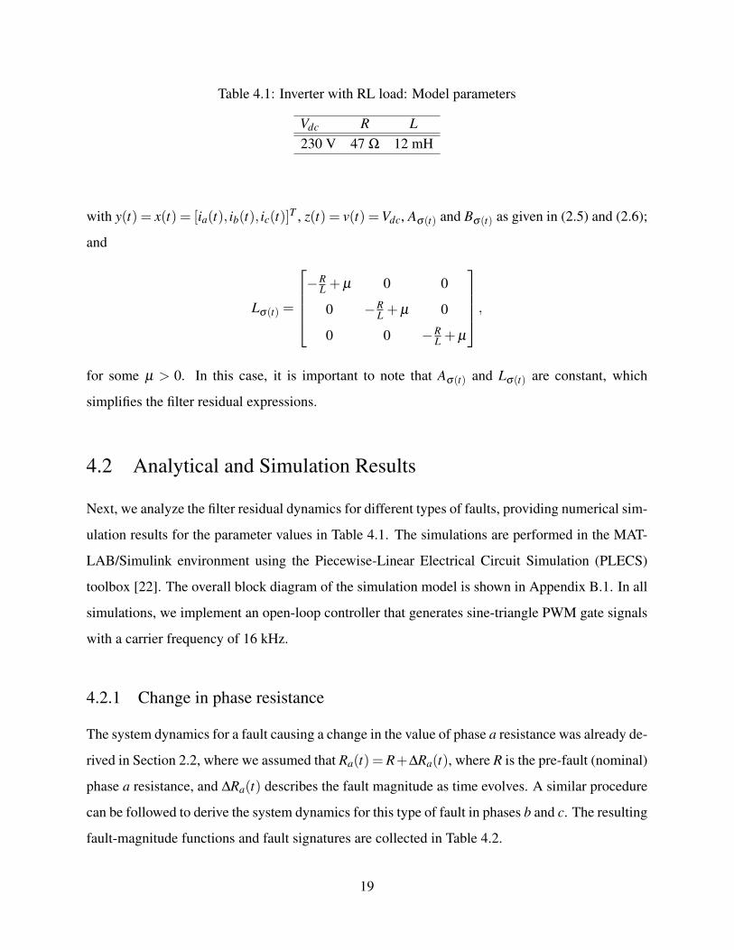
Table 4.1: Inverter with RL load: Model parameters
Vdc R L230 V 47 Ω 12 mH
with y(t) = x(t) = [ia(t), ib(t), ic(t)]T , z(t) = v(t) =Vdc, Aσ(t) and Bσ(t) as given in (2.5) and (2.6);
and
Lσ(t) =
−R
L +µ 0 0
0 −RL +µ 0
0 0 −RL +µ
,
for some µ > 0. In this case, it is important to note that Aσ(t) and Lσ(t) are constant, which
simplifies the filter residual expressions.
4.2 Analytical and Simulation Results
Next, we analyze the filter residual dynamics for different types of faults, providing numerical sim-
ulation results for the parameter values in Table 4.1. The simulations are performed in the MAT-
LAB/Simulink environment using the Piecewise-Linear Electrical Circuit Simulation (PLECS)
toolbox [22]. The overall block diagram of the simulation model is shown in Appendix B.1. In all
simulations, we implement an open-loop controller that generates sine-triangle PWM gate signals
with a carrier frequency of 16 kHz.
4.2.1 Change in phase resistance
The system dynamics for a fault causing a change in the value of phase a resistance was already de-
rived in Section 2.2, where we assumed that Ra(t) = R+∆Ra(t), where R is the pre-fault (nominal)
phase a resistance, and ∆Ra(t) describes the fault magnitude as time evolves. A similar procedure
can be followed to derive the system dynamics for this type of fault in phases b and c. The resulting
fault-magnitude functions and fault signatures are collected in Table 4.2.
19

0 0.02 0.04 0.06 0.08 0.1−2
−1.5
−1
−0.5
0
0.5
1
1.5
2
Time [s]
Filt
er R
esid
uals
γ1(t)
γ2(t)
γ3(t)
γ’1(t)
γ’2(t)
γ’3(t)
Figure 4.1: Inverter with RL load: Simulation of filter response for a fault causing phase c resis-tance to decrease by 5 Ω.
Table 4.2: Inverter with RL load: Fault magnitude function and signature for faults causingchanges in phase resistance.
i φi(t) fi
1 ∆Ra(t)3L ia(t) [−2,1,1]T
2 ∆Rb(t)3L ib(t) [1,−2,1]T
3 ∆Rc(t)3L ic(t) [1,1,−2]T
Now, following the notation in (3.5), the filter residual dynamics for a fault affecting phase c
resistance is given by
γ(t) = e−µte(0)+
tˆ
0
e−µ(t−τ)∆Rc(t)3L
ia(t)τ
f3, (4.2)
with f3 = [1,1,−2]T . Now, consider that at time t f a fault occurs causing the phase c resistance
to increase by ∆R > 0, i.e., ∆Rc(t) = ∆R, for all t > t f . While the phase currents are not perfectly
sinusoidal, the inductance of the RL load has some filtering effect; thus it is reasonable to assume
that ic(t)≈ I sin(ωt) for some I > 0 as t→ ∞. In the frequency domain, the current becomes
Ic(s) =ωI
s2 +ω2 .
Using the derivations done in Section3.2.5, the fault dynamics in the frequency domain can be
20
written as
E(s) =∆R(t)
3L1
s+uωI
s2 +ω2
which has the time domain response
γ(t) =I∆R(t)
3Lωe−µt−ωcos(ωt)+µsin(ωt)
ω2 +µ2 f .
Given a µ that is relatively large, the term ωe−µt will quickly reduce to zero, so the steady state
filter residual should be
γ(t)≈ γ(t) :=I∆R3L
µ sin(ωt)−ω cos(ωt)ω2 +µ2 f3. (4.3)
In the simulation environment, a fault causing the phase c resistance to change according
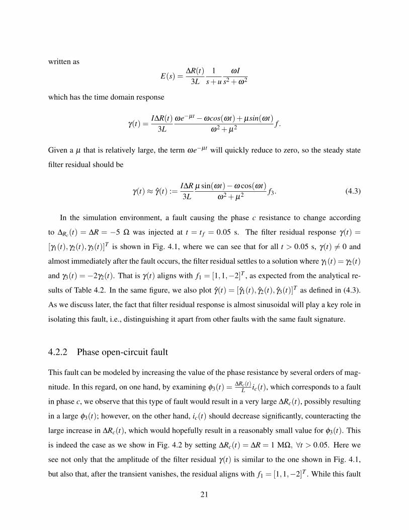
to ∆Rc(t) = ∆R = −5 Ω was injected at t = t f = 0.05 s. The filter residual response γ(t) =
[γ1(t),γ2(t),γ3(t)]T is shown in Fig. 4.1, where we can see that for all t > 0.05 s, γ(t) 6= 0 and
almost immediately after the fault occurs, the filter residual settles to a solution where γ1(t) = γ2(t)
and γ3(t) = −2γ2(t). That is γ(t) aligns with f1 = [1,1,−2]T , as expected from the analytical re-
sults of Table 4.2. In the same figure, we also plot γ(t) = [γ1(t), γ2(t), γ3(t)]T as defined in (4.3).
As we discuss later, the fact that filter residual response is almost sinusoidal will play a key role in
isolating this fault, i.e., distinguishing it apart from other faults with the same fault signature.
4.2.2 Phase open-circuit fault
This fault can be modeled by increasing the value of the phase resistance by several orders of mag-
nitude. In this regard, on one hand, by examining φ3(t) =∆Rc(t)
L ic(t), which corresponds to a fault
in phase c, we observe that this type of fault would result in a very large ∆Rc(t), possibly resulting
in a large φ3(t); however, on the other hand, ic(t) should decrease significantly, counteracting the
large increase in ∆Rc(t), which would hopefully result in a reasonably small value for φ3(t). This
is indeed the case as we show in Fig. 4.2 by setting ∆Rc(t) = ∆R = 1 MΩ, ∀t > 0.05. Here we
see not only that the amplitude of the filter residual γ(t) is similar to the one shown in Fig. 4.1,
but also that, after the transient vanishes, the residual aligns with f1 = [1,1,−2]T . While this fault
21

0 0.02 0.04 0.06 0.08 0.1−30
−20
−10
0
10
20
30
Time [s]
Filt
er R
esid
uals
γ1(t)
γ2(t)
γ3(t)
Figure 4.2: Inverter with RL load: Simulation of filter response for an open-circuit fault in phasec.
0 0.02 0.04 0.06 0.08 0.1−1.5
−1
−0.5
0
0.5
1
1.5
Time [s]
Filt
er R
esid
uals
γ1(t)
γ2(t)
γ3(t)
Figure 4.3: Inverter with RL load: Simulation of filter response for a fault causing phase c induc-tance to decrease by −5 mH.
has the same fault signature as a fault causing a change in the phase resistance, the filter response
is different; thus these two faults can be easily distinguished from each other. In particular, by
inspecting Figs. 4.1 and 4.2, we observe that the residual amplitude for the open-circuit fault is
more than 10 times greater than the amplitude for the resistance fault.
4.2.3 Change in phase inductance
As with phase c resistance fault, this fault can be modeled by describing the phase inductance as
Lc(t) = L+∆Lc(t), where L is the pre-fault phase c inductance, and ∆Lc(t) describes the fault
magnitude as time evolves. Deriving the post-fault dynamics is a bit more involved than in the re-
22
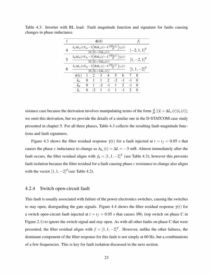
Table 4.3: Inverter with RL load: Fault magnitude function and signature for faults causingchanges in phase inductance.
i φi(t) fi
4λa∆La(t)Vdc−3
(R∆La(t)−L d∆La(t)
dt
)ia(t)
3L(3L+2∆La(t))[−2,1,1]T
5λb∆Lb(t)Vdc−3
(R∆Lb(t)−L d∆Lb(t)
dt
)ib(t)
3L(3L+2∆Lb(t))[1,−2,1]T
6λc∆Lc(t)Vdc−3
(R∆Lc(t)−L d∆Lc(t)
dt
)ic(t)
3L(3L+2∆Lc(t))[1,1,−2]T
σ(t) 1 2 3 4 5 6 7 8λa 0 1 1 2 -2 -1 -1 0λb 0 1 -2 -1 1 2 -1 0λc 0 -2 1 -1 1 -1 2 0
sistance case because the derivation involves manipulating terms of the form ddt [(L+∆Lc(t))ic(t)];
we omit this derivation, but we provide the details of a similar one in the D-STATCOM case study
presented in chapter 5. For all three phases, Table 4.3 collects the resulting fault-magnitude func-
tions and fault signatures.
Figure 4.3 shows the filter residual response γ(t) for a fault injected at t = t f = 0.05 s that
causes the phase c inductance to change as ∆Lc(t) = ∆L = −5 mH. Almost immediately after the
fault occurs, the filter residual aligns with f6 = [1,1,−2]T (see Table 4.3); however this prevents
fault isolation because the filter residual for a fault causing phase c resistance to change also aligns
with the vector [1,1,−2]T (see Table 4.2).
4.2.4 Switch open-circuit fault
This fault is usually associated with failure of the power electronics switches, causing the switches
to stay open, disregarding the gate signals. Figure 4.4 shows the filter residual response γ(t) for
a switch open-circuit fault injected at t = t f = 0.05 s that causes SW5 (top switch on phase C in
Figure 2.1) to ignore the switch signal and stay open. As with all other faults on phase C that were
presented, the filter residual aligns with f = [1,1,−2]T . However, unlike the other failures, the
dominant component of the filter response for this fault is not simply at 60 Hz, but a combinations
of a few frequencies. This is key for fault isolation discussed in the next section.
23

0 0.02 0.04 0.06 0.08 0.1−15
−10
−5
0
5
10
15
20
25
Time [s]
Filt
er R
esid
uals
γ1(t)
γ2(t)
γ3(t)
Figure 4.4: Inverter with RL load: Simulation of filter response for a fault causing SW5 to alwaysstay open.
4.2.5 Fault isolation
0 5000 10000 15000
−120
−100
−80
−60
−40
−20
0
20
40
60
Freq [Hz]
Filt
er R
esid
uals
[dB
]
Resistance decreaseInductance decreaseSW5 open−circuit fault
0 50 100 150 200
−40
−20
0
20
40
60
Freq [Hz]
Figure 4.5: Inverter with RL load: Frequency analysis of the filter residual response for faultsphase in c.
From the analysis above, it is obvious that once the fault occurs, it can be detected because the
filter residual is no longer zero. However, the fault signatures of all the components in each phase
are the same, e.g., for phase c, the resistance, inductance, and switches SW5 and SW6 (not analyzed
above) have the same fault signature [−2,1,1]T ; therefore by just analyzing the direction of the
filter residual we cannot distinguish these faults. A closer look at Figs. 4.1 and 4.3, corresponding
24
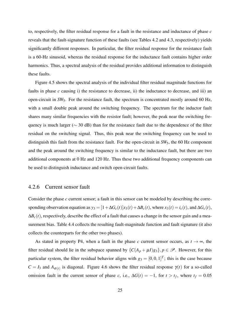
to, respectively, the filter residual response for a fault in the resistance and inductance of phase c
reveals that the fault-signature function of these faults (see Tables 4.2 and 4.3, respectively) yields
significantly different responses. In particular, the filter residual response for the resistance fault
is a 60-Hz sinusoid, whereas the residual response for the inductance fault contains higher order
harmonics. Thus, a spectral analysis of the residual provides additional information to distinguish
these faults.
Figure 4.5 shows the spectral analysis of the individual filter residual magnitude functions for
faults in phase c causing i) the resistance to decrease, ii) the inductance to decrease, and iii) an
open-circuit in SW5. For the resistance fault, the spectrum is concentrated mostly around 60 Hz,
with a small double peak around the switching frequency. The spectrum for the inductor fault
shares many similar frequencies with the resistor fault; however, the peak near the switching fre-
quency is much larger (∼ 30 dB) than for the resistance fault due to the dependence of the filter
residual on the switching signal. Thus, this peak near the switching frequency can be used to
distinguish this fault from the resistance fault. For the open-circuit in SW5, the 60 Hz component
and the peak around the switching frequency is similar to the inductance fault, but there are two
additional components at 0 Hz and 120 Hz. Thus these two additional frequency components can
be used to distinguish inductance and switch open-circuit faults.
4.2.6 Current sensor fault
Consider the phase c current sensor; a fault in this sensor can be modeled by describing the corre-
sponding observation equation as y3 = [1+∆Gc(t)]x3(t)+∆Bc(t), where x3(t) = ic(t), and ∆Gc(t),
∆Bc(t), respectively, describe the effect of a fault that causes a change in the sensor gain and a mea-
surement bias. Table 4.4 collects the resulting fault-magnitude function and fault signature (it also
collects the counterparts for the other two phases).
As stated in property P4, when a fault in the phase c current sensor occurs, as t → ∞, the
filter residual should lie in the subspace spanned by C(Ap + µI)g3, p ∈P . However, for this
particular system, the filter residual behavior aligns with g3 = [0,0,1]T ; this is the case because
C = I3 and Aσ(t) is diagonal. Figure 4.6 shows the filter residual response γ(t) for a so-called
omission fault in the current sensor of phase c, i.e., ∆G(t) = −1, for t > t f , where t f = 0.05
25
0 0.02 0.04 0.06 0.08 0.1−20
−15
−10
−5
0
5
10
15
20
Time [s]
Filt
er R
esid
uals
γ1(t)
γ2(t)
γ3(t)
Figure 4.6: Inverter with RL load: Simulation of filter response for an omission fault in phase ccurrent sensor.
Table 4.4: Inverter with RL load: Fault magnitude function and signature for faults in currentsensors.
i θi(t) gi
1(−R
L +µ)
∆Ga(t)(ia(t)+∆Ba(t)) [1,0,0]T
2(−R
L +µ)
∆Gb(t)(ib(t)+∆Bb(t)) [0,1,0]T
3(−R
L +µ)
∆Gc(t)(ic(t)+∆Bc(t)) [0,0,1]T
s, and ∆B(t) = 0, ∀t. As expected, almost immediately after the fault, the residual aligns with
g3 = [0,0,1]T .
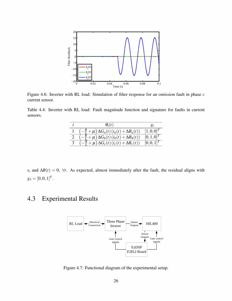
4.3 Experimental Results
RL LoadThree Phase
InvererElectrical
ConnectionHIL400
Sensor
Outputs
EzDSP
F2812 Board
Sensor
OutputsGate control
signalsGate control
signals
Figure 4.7: Functional diagram of the experimental setup.
26
Ezdsp F2812
Control Board
Typhoon
HIL400
Modular Inverter
Power Board
Resistor Boxs
Inductors
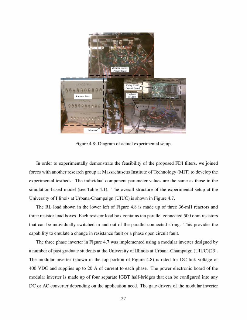
Figure 4.8: Diagram of actual experimental setup.
In order to experimentally demonstrate the feasibility of the proposed FDI filters, we joined
forces with another research group at Massachusetts Institute of Technology (MIT) to develop the
experimental testbeds. The individual component parameter values are the same as those in the
simulation-based model (see Table 4.1). The overall structure of the experimental setup at the
University of Illinois at Urbana-Champaign (UIUC) is shown in Figure 4.7.
The RL load shown in the lower left of Figure 4.8 is made up of three 36-mH reactors and
three resistor load boxes. Each resistor load box contains ten parallel connected 500 ohm resistors
that can be individually switched in and out of the parallel connected string. This provides the
capability to emulate a change in resistance fault or a phase open circuit fault.
The three phase inverter in Figure 4.7 was implemented using a modular inverter designed by
a number of past graduate students at the University of Illinois at Urbana-Champaign (UIUC)[23].
The modular inverter (shown in the top portion of Figure 4.8) is rated for DC link voltage of
400 VDC and supplies up to 20 A of current to each phase. The power electronic board of the
modular inverter is made up of four separate IGBT half-bridges that can be configured into any
DC or AC converter depending on the application need. The gate drivers of the modular inverter
27

protect the IGBT switches against over-voltage, short-circuit, and gate faults. Aside from the
optical and magnetic isolation of the sensors, all connections between the power electronic board
and control platform are differential, which further protects the low-voltage control circuits from
the high-voltage power board. To further protect against human error, dead time generation is
automatically done through a Complex Programmable Logic Device (CPLD) on the power board.
There are two ribbon cables that connect the power board with a low-voltage control board, one
for analog and one for digital signals. While the analog pin out in fixed, the digital signals can be
modified through another CPLD on the control board. The control board provides analog signal
conditioning and digital signals routing between the power stage and the control. In addition, the
control board contains toggle switches that supply 5 different enable signals to the power stage,
one for each of the four IGBT half-bridges and a master enable.
The HIL400 system shown in the bottom right corner of Figure 4.8 is an FPGA-based power
electronics simulator developed by our partner group at MIT that runs the real-time FDI filter
in lock-step with hardware circuits. They use the generalized automaton modeling approach de-
scribed in [20], which, among other things, enables the implementation of the linear-switched
state-space model in defining the FDI filter. During real-time execution, a direct memory indexing
technique controls the selection of the active mode based on the system input v(t) and boundary
conditions defined by y(t). A linear solver computes the state vector x(t) and the corresponding
estimated output vector y(t), and filter residual γ(t). An internal signal generator and external ana-
log and digital input ports provide the input vector v(t) to the state-space solver. The state vector
x(t) and the output vector y(t) are accessible in real-time through low-latency analog output ports.
The processor architecture, which is implemented in an FPGA device, guarantees the duration
of execution for each time interval to be shorter than the fixed simulation time step, resulting in
real-time performance regardless of the size of the system. Furthermore, the loop-back latency is
minimized with custom designed input-output hardware, and has been characterized to be on the
order of 1 µs [24].
The control platform for the experimental testbed is the Ezdsp F2812 board from Spectrum
Digital shown in the right side of Figure 4.8. The F2812 is a 32 bit fixed-point digital signal
controller (DSC) with clock frequency of 150 Mhz. This TI DSC was specifically designed for
three phase motor drive operation and feedback control of three-phase inverters, making it a very
28
suitable choice for our needs. The control algorithms were built using Matlab/Simulink and Matlab
Embedded Coder. The Matlab Embedded Coder is a library for Matlab which allows Matlab
code to be translated into C code. In addition, the Embedded Coder contains processor specific
blocks for Simulink which allows translation of a Simulink control flow-diagram into processor-
specific C code. To construct our controllers and observer, the flow-diagram of the entire control is
first built in Simulink using a combination of Simulink blocks and processor-specific blocks from
Matlab Embedded Coder. When the Simulink model is compiled, processor specific code for this
particular DSC is generated which can be directly loaded into the DSC.
A very similar setup was also built by the team at MIT. The results presented next were done
by the MIT group, but the same experiments were verified with the setup at UIUC.
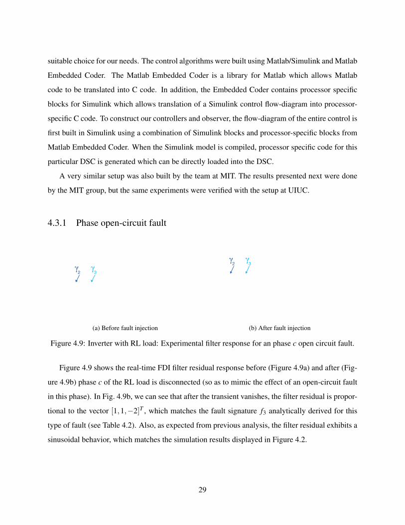
4.3.1 Phase open-circuit fault
(a) Before fault injection (b) After fault injection
Figure 4.9: Inverter with RL load: Experimental filter response for an phase c open circuit fault.
Figure 4.9 shows the real-time FDI filter residual response before (Figure 4.9a) and after (Fig-
ure 4.9b) phase c of the RL load is disconnected (so as to mimic the effect of an open-circuit fault
in this phase). In Fig. 4.9b, we can see that after the transient vanishes, the filter residual is propor-
tional to the vector [1,1,−2]T , which matches the fault signature f3 analytically derived for this
type of fault (see Table 4.2). Also, as expected from previous analysis, the filter residual exhibits a
sinusoidal behavior, which matches the simulation results displayed in Figure 4.2.
29

4.3.2 Current sensor fault
Figure 4.10: Inverter with RL load: Experimental filter response for an omission fault in phase ccurrent sensor.
Figure 4.10 displays the real-time response of the FDI filter after the current sensor of phase
c is disconnected. The filter residual matches the simulation results shown in Fig. 4.6. As in the
simulations, after the transient vanishes, the filter residual aligns with the vector [0,0,1]T , which
matches the fault signature g3 analytically derived for this fault (see Table 4.4).
30

Chapter 5
DESIGN AND ANALYSIS OF A FDI FILTER FOR AD-STATCOM
SupplyLine
ImpedanceLoad
DSTATCOM
Control and FDI Filter
Sensors
Figure 5.1: D-STATCOM simulation block diagram.
In this chapter, we develop a FDI filter for a Distributed Static Compensator (D-STATCOM) of
Fig. 5.1. A D-STATCOM is a lower-voltage distribution-level controller that is often tied to highly
nonlinear loads to reduce their disturbance to the grid, or to custom power loads that require very
strict power quality control [9, 10]. The most basic D-STATCOM system consists of a voltage
source converter with the DC end tied to a capacitor and the AC end connected in shunt to the
power distribution network through a coupling transformer (see Fig. 5.1).
Much of the same analysis done for the inverter with RL load system applies here, but the DC
link capacitor, and sinusoidal voltage inputs add some interesting behaviors. As before, we provide
analytical expressions for individual component fault signatures and associated fault-magnitude
functions; we also test the performance of the FDI filter in a simulation environment.
31
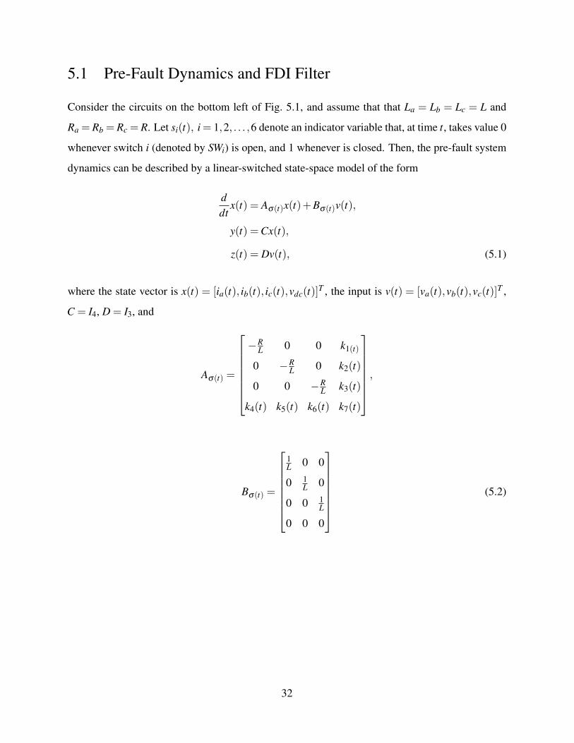
5.1 Pre-Fault Dynamics and FDI Filter
Consider the circuits on the bottom left of Fig. 5.1, and assume that that La = Lb = Lc = L and
Ra = Rb = Rc = R. Let si(t), i = 1,2, . . . ,6 denote an indicator variable that, at time t, takes value 0
whenever switch i (denoted by SWi) is open, and 1 whenever is closed. Then, the pre-fault system
dynamics can be described by a linear-switched state-space model of the form
ddt
x(t) = Aσ(t)x(t)+Bσ(t)v(t),
y(t) =Cx(t),
z(t) = Dv(t), (5.1)
where the state vector is x(t) = [ia(t), ib(t), ic(t),vdc(t)]T , the input is v(t) = [va(t),vb(t),vc(t)]T ,
C = I4, D = I3, and
Aσ(t) =
−R
L 0 0 k1(t)
0 −RL 0 k2(t)
0 0 −RL k3(t)
k4(t) k5(t) k6(t) k7(t)
,
Bσ(t) =
1L 0 0
0 1L 0
0 0 1L
0 0 0
(5.2)
32
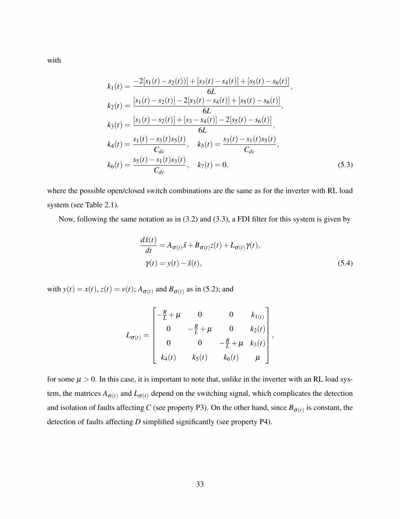
with
k1(t) =−2[s1(t)− s2(t))]+ [s3(t)− s4(t)]+ [s5(t)− s6(t)]
6L,
k2(t) =[s1(t)− s2(t)]−2[s3(t)− s4(t)]+ [s5(t)− s6(t)]
6L,
k3(t) =[s1(t)− s2(t)]+ [s3− s4(t)]−2[s5(t)− s6(t)]
6L,
k4(t) =s1(t)− s3(t)s5(t)
Cdc, k5(t) =
s3(t)− s1(t)s5(t)Cdc
,
k6(t) =s5(t)− s1(t)s3(t)
Cdc, k7(t) = 0, (5.3)
where the possible open/closed switch combinations are the same as for the inverter with RL load
system (see Table 2.1).
Now, following the same notation as in (3.2) and (3.3), a FDI filter for this system is given by
dx(t)dt
= Aσ(t)x+Bσ(t)z(t)+Lσ(t)γ(t),
γ(t) = y(t)− x(t), (5.4)
with y(t) = x(t), z(t) = v(t); Aσ(t) and Bσ(t) as in (5.2); and
Lσ(t) =
−R
L +µ 0 0 k1(t)
0 −RL +µ 0 k2(t)
0 0 −RL +µ k3(t)
k4(t) k5(t) k6(t) µ
,
for some µ > 0. In this case, it is important to note that, unlike in the inverter with an RL load sys-
tem, the matrices Aσ(t) and Lσ(t) depend on the switching signal, which complicates the detection
and isolation of faults affecting C (see property P3). On the other hand, since Bσ(t) is constant, the
detection of faults affecting D simplified significantly (see property P4).
33
0.4 0.45 0.5 0.55 0.6−2
−1
0
1
2
3
Time [s]
Filt
er R
esid
uals
γ1(t)
γ2(t)
γ3(t)
γ4(t)
Figure 5.2: D-STATCOM: Simulation of filter response for 50% decrease in DC link capacitance.
5.2 Analytical and Simulation Results
Next, we analyze the filter residual dynamics for different types of faults, providing numerical
simulation results for the parameter values in Table 5.1; the simulations are performed in Mat-
lab/Simulink/PLECS. The overall block diagram of the simulation model is shown in Appendix
B.2. Figure 5.1 provides a block diagram of the simulation model; the supply block is comprised
of a three-phase ideal voltage source, the line impedance block is a series-connection of induc-
tors and resistors, whereas the load block is comprised of inductive reactances. The controller is
adapted from the voltage-mode controller in [25]. This controller includes a phase-lock loop that
generates sine-triangle PWM gate signals with a carrier frequency of 5 kHz.
5.2.1 Change in dc link capacitance
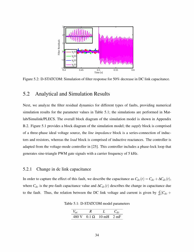
In order to capture the effect of this fault, we describe the capacitance as Cdc(t) =Cdc +∆Cdc(t),
where Cdc is the pre-fault capacitance value and ∆Cdc(t) describes the change in capacitance due
to the fault. Thus, the relation between the DC link voltage and current is given by ddt [Cdc +
Table 5.1: D-STATCOM model parameters
Vac R L Cdc
480 V 0.1 Ω 10 mH 2 mF
34
∆Cdc(t)]vdc =−idc(t), from where it follows that
dvdc(t)dt
=1
Cdc +∆Cdc(t)
(idc(t)−
d∆Cdc(t)dt
vdc(t))
;
therefore, the post-fault dynamics can be described by
dx(t)dt
= Aσ x(t)+ Bσ v(t), (5.5)
with Bσ = Bσ , and
Aσ =
−R
L 0 0 k1(t)
0 −RL 0 k2(t)
0 0 −RL k3(t)
k4(t) k5(t) k6(t) k7(t)
, (5.6)
where k1(t)–k3(t) are the same as in (5.3), and
k4(t) =s1(t)− s3(t)s5(t)
Cdc +∆Cdc(t),
k5(t) =s3(t)− s1(t)s5(t)
Cdc +∆Cdc(t),
k6(t) =s5(t)− s1(t)s3(t)
Cdc +∆Cdc(t),
k7(t) =−ddt ∆Cdc(t)
Cdc +∆Cdc(t). (5.7)
Now, by rearranging (5.6) as in (2.9), we obtain the fault signature f1, and the fault-magnitude
function φ1(t), both of which are given in Table 5.2.
Figure 5.2 shows the filter residual response for a fault causing a decrease of 50 % in the DC
link capacitance injected at t f = 0.5 s. As expected, after the initial transient, the filter residual
aligns with the f1 = [0,0,0,1]T .
35
0.4 0.45 0.5 0.55 0.6 0.65−15
−10
−5
0
5
10
15
Time [s]
Filt
er R
esid
uals
γ1(t)
γ2(t)
γ3(t)
γ4(t)
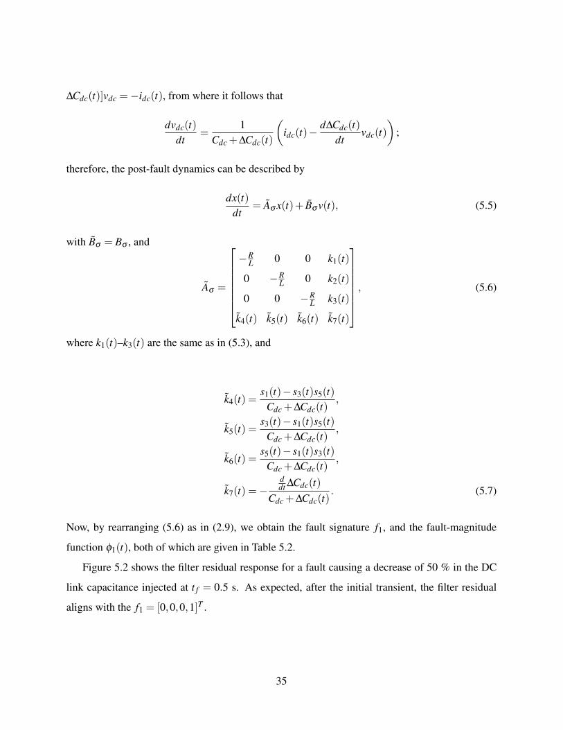
Figure 5.3: D-STATCOM: Simulation of filter response for a fault causing phase c resistance tochange from 0.1 Ω to 0.5 Ω.
Table 5.2: D-STATCOM: Fault magnitude function and signature for faults in DC link capacitor.
φ1(t) f1
λ∆Cdc(t)idc−C d∆Cdc(t)
dt vdcCdc[Cdc+∆Cdc(t)]
[0,0,0,1]T
σ(t) 1 2 3 4 5 6 7 8idc 0 ic ib ia ia ib ic 0λ 0 -1 -1 1 -1 1 1 0
5.2.2 Change in phase resistance
For this type of fault, it is clear from (5.2) that only the equations for the phase current will be
altered; in fact the derivation of the post-fault model is very similar to the one for the inverter
with RL load model derived in Section 2.2; thus, we omit it. Therefore, the fault magnitude
functions φi(t), i = 2,3,4 are the same as the corresponding ones in Table 4.2; however, the fault
signatures are 4-dimensional vectors instead of 3-dimensional vectors, but the first three entries of
each fi, i = 2,3,4 coincide with the corresponding fault signature vectors in Table 4.2, with the
fourth entry equal to zero for all fi’s, e.g., f2 = [−2,1,1,0]T . In the simulation environment, a fault
causing the resistance of phase c to change from 0.1 Ω to 0.5 Ω is injected at t f = 0.5 s; Fig. 5.3
shows the evolution of the filter residual; after the transient vanishes, the filter residual aligns with
f2 = [1,1,−2,0]T .
36
Table 5.3: D-STATCOM: Fault magnitude function and signature for switch open-circuit faults.
Fault φi(t) fi
SW1 (i = 8) −vdc(t)[s4(t)+s6(t)]−3Ria(t)6 [−2,1,1,0]T
SW2 (i = 9) vdc(t)[s3(t)+s5(t)]−3Ria(t)6 [−2,1,1,0]T
SW3 (i = 10) −vdc(t)[s2(t)+s6(t)]−3Rib(t)6 [1,−2,1,0]T
SW4 (i = 11) vdc(t)[s1(t)+s5(t)]−3Rib(t)6 [1,−2,1,0]T
SW5 (i = 12) −vdc(t)[s2(t)+s4(t)]−3Ric(t)6 [1,1,−2,0]T
SW6 (i = 13) vdc(t)[s1(t)+s3(t)]−3Ric(t)6 [1,1,−2,0]T
5.2.3 Other faults
Table 5.3 shows the fault-magnitude functions and fault signatures for switch open-circuit faults;
the ones for phase inductance faults and sensor faults are similar to the corresponding ones for the
inverter with RL load system; therefore, they are omitted. As with that system, the fault signatures
for all the components in the same phase are identical; thus to distinguish them, it is necessary
to analyze the frequency spectrum of the individual filter responses, with similar results to those
in Section 4.2.5. The D-STATCOM fault dynamics for the various faults were derived using the
Symbolic Math Toolbox in Matlab, the script used to derive the capacitor, inductor and switch
fault residuals are shown in Appendix A.
5.3 Real-Time Simulation Results
The fault detection filter for D-STATCOM was verified using the HIL400 power electronics sim-
ulator and the Ezdsp F2812 Board. For this setup, the HIL400 power electronics simulator was
used as the physical plant with the F2812 DSC acting as both the control and the fault detection
filter.
The basic structure of this setup is shown in Figure 5.4. In this arrangement, the HIL400
system runs a real-time simulation of a D-STATCOM system with parameters given in Table 5.1.
The HIL400 takes in switch control signals from the DSC and outputs the simulated currents and
voltages back to the DSC. The DSC runs the control as well as the fault detection filter.
37
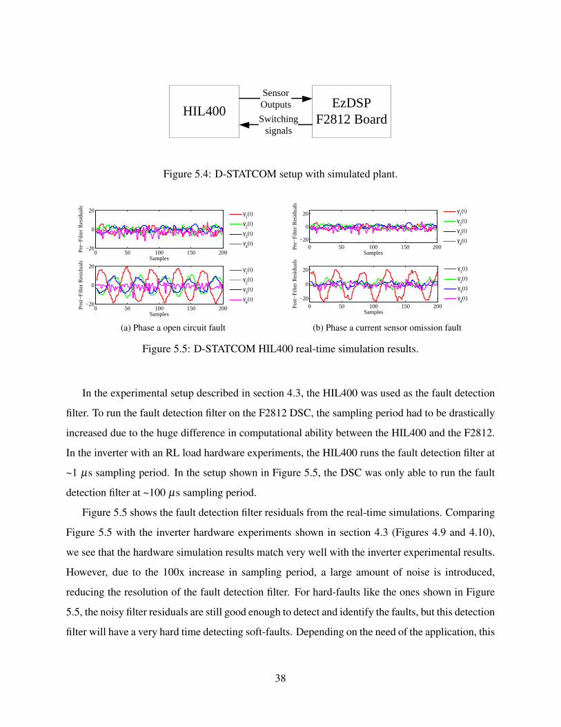
Sensor
Outputs EzDSP
F2812 BoardSwitching
signals
HIL400
Figure 5.4: D-STATCOM setup with simulated plant.
0 50 100 150 200−20
0
20
Samples
Pre
−F
ilter
Res
idua
ls
γ1(t)
γ2(t)
γ3(t)
γ4(t)
0 50 100 150 200−20
0
20
Samples
Pos
t−F
ilter
Res
idua
ls
γ1(t)
γ2(t)
γ3(t)
γ4(t)
(a) Phase a open circuit fault
0 50 100 150 200−20
0
20
Samples
Pre
−F
ilter
Res
idua
ls
γ1(t)
γ2(t)
γ3(t)
γ4(t)
0 50 100 150 200−20
0
20
Samples
Pos
t−F
ilter
Res
idua
ls
γ1(t)
γ2(t)
γ3(t)
γ4(t)
(b) Phase a current sensor omission fault
Figure 5.5: D-STATCOM HIL400 real-time simulation results.
In the experimental setup described in section 4.3, the HIL400 was used as the fault detection
filter. To run the fault detection filter on the F2812 DSC, the sampling period had to be drastically
increased due to the huge difference in computational ability between the HIL400 and the F2812.
In the inverter with an RL load hardware experiments, the HIL400 runs the fault detection filter at
~1 µs sampling period. In the setup shown in Figure 5.5, the DSC was only able to run the fault
detection filter at ~100 µs sampling period.
Figure 5.5 shows the fault detection filter residuals from the real-time simulations. Comparing
Figure 5.5 with the inverter hardware experiments shown in section 4.3 (Figures 4.9 and 4.10),
we see that the hardware simulation results match very well with the inverter experimental results.
However, due to the 100x increase in sampling period, a large amount of noise is introduced,
reducing the resolution of the fault detection filter. For hard-faults like the ones shown in Figure
5.5, the noisy filter residuals are still good enough to detect and identify the faults, but this detection
filter will have a very hard time detecting soft-faults. Depending on the need of the application, this
38

trade-off between filter resolution and computational cost could be designed to achieve a balance
between cost and reliability of the system. In applications where slight degradations in individual
components need to monitored, a processor like the HIL400 might be preferred, but in low cost
applications that only need protection against hard-faults, then maybe a processor like the F2812
is enough. A study of the filter noise is presented later in section 6, but much more work is needed
to fully address the issue.
The key insight that this setup demonstrates is the fact that it is possible to implement our
fault detection filter in a real-world setting without any change to the existing hardware setup. The
F2812 is a relatively inexpensive control platform (~$20 per chip). If the fault detection filter can
be implemented along with the control on the F2812 DSC, then it should be easy to implement
high resolution fault detection filters in high-end control platforms used in industry.
39

Chapter 6
IMPLEMENTATION CONSTRAINTS
6.1 Noise and Delay Modeling
After the fault detection filter methodology was shown to be effective in the ideal case, we added
realistic implementation constraints to better study their effects on the overall system. The two
major issues are sampling frequency and sensor parasitic. The sampling frequency is mainly de-
termined by the Analog to Digital Converter (ADC) sampling frequency and processor speed. To
study the effect of sampling frequency, simulations were run with the detection filter sampling at
fixed frequencies. The steady-state RMS value of the error residual over 30 cycles (0.5 second)
was calculated and plotted vs. the sampling frequency in Figure 6.1. The results show that filter
error decreases linearly with respect to the sampling frequency. This general trend could be very
useful in balancing between fault detection filter resolution and computational complexity.
However, the actual dynamics of the noise are more complex than a linear dependence on
sampling frequency because simulations assumed a constant filter gain µ for all frequencies. If the
value of µ is also optimized, it is possible that much higher resolution can be achieved at lower
sampling frequencies.
Aside from sampling time, sensor related issues can also cause problems. Some common
sensor issues include signal gain, bias, delay, and bandwidth. Gain and bias issues are mostly
caused by calibration, which can be mitigated if the sensors are carefully tuned. Bandwidth issues
are usually intrinsic to the sensor itself. Since the D-STATCOM usually operates at relatively slow
switching frequencies, these issues can be avoided through careful selection of system sensors.
Delay is the most problematic because it can be caused by analog filters inserted between the
sensor and the ADC, long wires, or digital filters used in the control loop. This issue is difficult
40
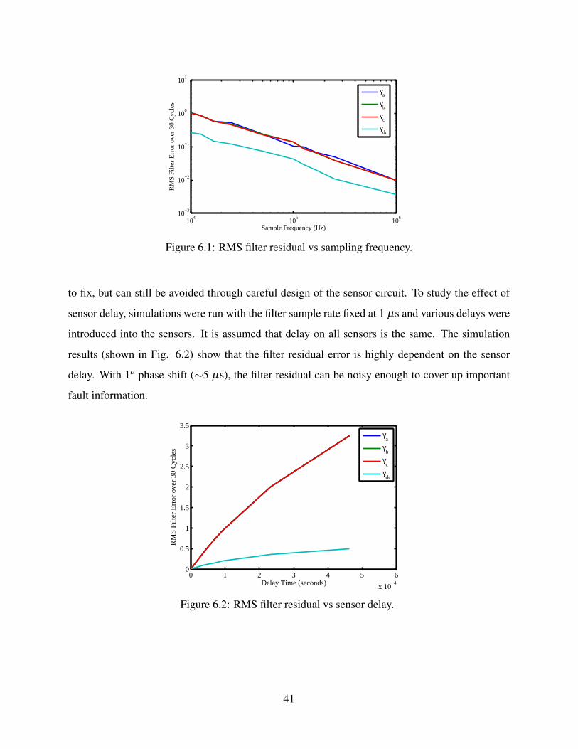
104
105
106
10−3
10−2
10−1
100
101
Sample Frequency (Hz)
RM
S F
ilter
Err
or o
ver
30 C
ycle
s
γa
γb
γc
γdc
Figure 6.1: RMS filter residual vs sampling frequency.
to fix, but can still be avoided through careful design of the sensor circuit. To study the effect of
sensor delay, simulations were run with the filter sample rate fixed at 1 µs and various delays were
introduced into the sensors. It is assumed that delay on all sensors is the same. The simulation
results (shown in Fig. 6.2) show that the filter residual error is highly dependent on the sensor
delay. With 1o phase shift (∼5 µs), the filter residual can be noisy enough to cover up important
fault information.
0 1 2 3 4 5 6
x 10−4
0
0.5
1
1.5
2
2.5
3
3.5
Delay Time (seconds)
RM
S F
ilter
Err
or o
ver
30 C
ycle
s
γa
γb
γc
γdc
Figure 6.2: RMS filter residual vs sensor delay.
41
6.2 Parameter Estimation and Sensitivity Analysis
While the model shown in Fig. 2.1 captures the overall operation of the D-STATCOM, it does
not take into consideration parasitics such as Capacitor ESR, switch on-state voltage, switch re-
sistances, etc. There are also sensor noise and quantization errors; all these will add noise to the
system. This means that even during pre-fault operation, the filter residual is not expected to be
zero. Also, due to the existence of parasitics, the component parameters shown in Fig. 2.1 will be
slightly different from measured values in the actual system. In order to reduce noise created by
parasitics, a method to estimate component parameters is needed.
One way to deal with this issue is to first determine some initial guesses for component values
through physical measurements, then use an optimization algorithm to iteratively determine the
parameter values that minimize the filter error over a period of time. Mathematically, this can be
stated as
minimizeˆ t f
t0|e(t)|
sub ject toH[
R L Cdc
]T≤ k
where t0 < t < t f defines some predetermined time period while matrix H and vector k define
the upper and lower limits on the component values. The final component values found through
this method might be a little different from physical measurements, but are guaranteed to minimize
noise in the filter residual. The key parameter that determines the effectiveness of such an approach
is the sensitivity of the filter residual to the values of R, L, and Cdc. To study the relative sensitivities
of the three parameters, simulations of un-faulted detection filter noise were integrated over 0.5
s (30 cycles) for various different values of R, L, and Cdc. The simulations results are plotted in
Fig. 6.3. The results show that the filter residue is most sensitive to the value of inductance L
and least sensitive to the value of the DC link capacitance Cdc. The objective function is convex
as the inductance and resistance value approaches the actual circuit parameter values. This means
that given rough initial measurements, it is possible to iteratively determine the inductance L and
resistance R that minimizes the filter residue. However, due to the extremely low sensitivity of
the filter residue to the value of capacitance, it is best that the capacitance be physically measured
42

0
0.5
1
00.002
0.0040.006
0.0080.01
0
0.5
1
1.5
2
2.5
3
3.5
x 105
Resistance [Ω]
Inductance [H]
Tot
al F
ilter
Res
idue
0.20.4
0.60.8
12
4
6
8
10
x 10−3
1
1.5
2
2.5
3
3.5
x 104
Resistance [Ω]
Capacitance [F]
Tot
al F
ilter
Res
idue
00.002
0.0040.006
0.0080.01 0
0.002
0.004
0.006
0.008
0.01
0
1
2
3
4
x 105
Capacitance [F]
Inductance [H]
Tot
al F
ilter
Res
idua
l
Figure 6.3: Parameter sensitivity simulation results: (a) resistance vs inductance, (b) resistance vscapacitance, and (c) inductance vs capacitance.
instead of using the optimization approach.
43

Chapter 7
CONCLUSIONS
In this thesis, observer-based fault detection filters were presented for D-STATCOM, but the ap-
proach can be easily adopted to any power electronics device. In the absence of fault, the detection
filter asymptotically converges to the state variable actual values. When a fault occurs, the esti-
mated values diverge from the state variable actual values, and the filter residual error accurately
determines the location and extent of the faults. Simulation results show that the filter is able to
capture a wide range of component failures and provide a good estimate for degradation in circuit
components. The proposed detection filter can also be easily modified to perform fault detection
or even control-related functions in a wide range of AD/DC or DC/AC power electronics systems
including FACTS devices, HVDC systems, motor drives, solar inverters, etc. Simulation results
were presented which demonstrate the effectiveness of the detection filter for identifying compo-
nent degradation. Initial experimentation was done to demonstrate the feasibility of the approach
in existing control platforms.
44

REFERENCES
[1] R. J. Patton, P. M. Frank, and R. N. Clarke, Eds., Fault diagnosis in dynamic systems: theoryand application. Upper Saddle River, NJ, USA: Prentice-Hall, Inc., 1989.
[2] D. Zhang, F. Wang, R. Burgos, J. Kern, S. El-Barbari, and D. Boroyevich, “Internal faultdetection and isolation for paralleled voltage source converters,” in Proc. of IEEE AppliedPower Electronics Conference and Exposition, Washington, DC, 2009, pp. 833–839.
[3] K. Levin, E. Hope, and A. Domínguez-García, “Observer-based fault diagnosis of powerelectronics systems,” in Proceedings of IEEE Energy Conversion Congress and Exposition,Atlanta, GA, 2010, pp. 4434 – 4440.
[4] S. Khomfoi and L. Tolbert, “Fault diagnosis and reconfiguration for multilevel inverter driveusing AI-based techniques,” IEEE Transactions on Industrial Electronics, vol. 54, no. 6, pp.2954 –2968, 2007.
[5] F. Chowdhury and J. Aravena, “A modular methodology for fast fault detection and classifi-cation in power systems,” IEEE Transactions on Control Systems Technology, vol. 6, no. 5,pp. 623–634, Sept. 1998.
[6] B. Singh, S. Murthy, and S. Gupta, “Analysis and design of STATCOM-based voltage regula-tor for self-excited induction generators,” IEEE Transactions on Energy Conversion, vol. 19,no. 4, pp. 783 – 790, 2004.
[7] D. Soto and T. Green, “A comparison of high-power converter topologies for the implemen-tation of facts controllers,” IEEE Transactions on Industrial Electronics, vol. 49, no. 5, pp.1072 – 1080, 2002.
[8] A. Yazdani, H. Sepahvand, M. Crow, and M. Ferdowsi, “Fault detection and mitigation inmultilevel converter STATCOMs,” IEEE Transactions on Industrial Electronics, vol. 58,no. 4, pp. 1307 –1315, Apr. 2011.
[9] T. Manmek, C. Mudannayake, and C. Grantham, “Voltage dip detection based on an efficientleast squares algorithm for D-STATCOM application,” in Power Electronics and Motion Con-trol Conference, 2006. IPEMC 2006. CES/IEEE 5th International, vol. 2, Aug. 2006, pp. 1 –6.
[10] G. Reed, M. Takeda, and I. Iyoda, “Improved power quality solutions using advanced solid-state switching and static compensation technologies,” in Proc. of IEEE Power Eng. SocietyWinter Meeting, vol. 2, New York, NY, USA, 1999, pp. 1132 – 1137.
45
[11] S. Karimi, P. Poure, and S. Saadate, “Fast power switch failure detection for fault tolerantvoltage source inverters using FPGA,” IET Power Electronics, vol. 2, no. 4, pp. 346 –354,July 2009.
[12] R. de Araujo Ribeiro, C. Jacobina, E. da Silva, and A. Lima, “Fault detection of open-switchdamage in voltage-fed PWM motor drive systems,” IEEE Transactions on Power Electronics,vol. 18, no. 2, pp. 587 – 593, Mar. 2003.
[13] R. Peuget, S. Courtine, and J.-P. Rognon, “Fault detection and isolation on a PWM inverterby knowledge-based model,” IEEE Transactions on Industry Applications, vol. 34, no. 6, pp.1318 –1326, Nov/Dec. 1998.
[14] C. Turpin, P. Baudesson, F. Richardeau, F. Forest, and T. Meynard, “Fault management ofmulticell converters,” IEEE Transactions on Industrial Electronics, vol. 49, no. 5, pp. 988 –997, 2002.
[15] S. Khomfoi and L. Tolbert, “Fault diagnostic system for a multilevel inverter using a neuralnetwork,” IEEE Transactions on Power Electronics, vol. 22, no. 3, pp. 1062 –1069, May2007.
[16] G. F. Franklin, M. L. Workman, and D. Powell, Digital Control of Dynamic Systems, 3rd ed.Boston, MA, USA: Addison-Wesley Longman Publishing Co., Inc., 1997.
[17] D. Luenberger, Ed., Introduction to Dynamic Systems. New York, NY: John Wiley, 1979.
[18] D. Liberzon, Switching in Systems and Control. Boston, MA: Birkhauser, 2003.
[19] D. Majstorovic, Z. Pele, A. Kovacevic, and N. Celanovic, “Computer based emulation ofpower electronics hardware,” in Proc. IEEE Eastern European Conf. the Engineering of Com-puter Based Systems, Novi Sad, Serbia, 2009, pp. 56–64.
[20] D. Majstorovic, I. Celanovic, N. Teslic, N. Celanovic, and V. Katic, “Ultralow-latencyhardware-in-the-loop platform for rapid validation of power electronics designs,” IEEETransactions on Industrial Electronics, vol. 58, no. 10, pp. 4708 – 4716, Oct. 2011.
[21] A. Tanwani, A. Dominguez-Garcia, and D. Liberzon, “An inversion-based approach to faultdetection and isolation in switching electrical networks,” IEEE Transactions on Control Sys-tems Technology, vol. 19, no. 5, pp. 1059 –1074, Sep. 2011.
[22] J. Alimeling and W. Hammer, “PLECS-piece-wise linear electrical circuit simulation forSimulink,” in Proceedings of the IEEE International Conference on Power Electronics andDrive Systems, 1999.
[23] J. Kimball, M. Amrhein, A. Kwasinski, J. Mossoba, B. Nee, Z. Sorchini, W. Waever, J. Wells,and G. Zhang, Modular Inverter System Specifications. Urbana, IL, USA: Grainger Centerfor Electric Machinery and Electromechanics, 2006.
46

[24] M. Vekic, S. Grabic, D. Majstorovic, I. Celanovic, N. Celanovic, and V. Katic, “Ultra lowlatency hil platform for rapid development of complex power electronics systems,” IEEETransactions on Power Electronics, vol. PP, no. 99, p. 1, 2012.
[25] N. Hingorani and L. Gyugyi, Understanding FACTS (Concepts and Technology of FlexibleAC Transmission Systems). Hoboken, NJ: IEEE Press, 1999.
47
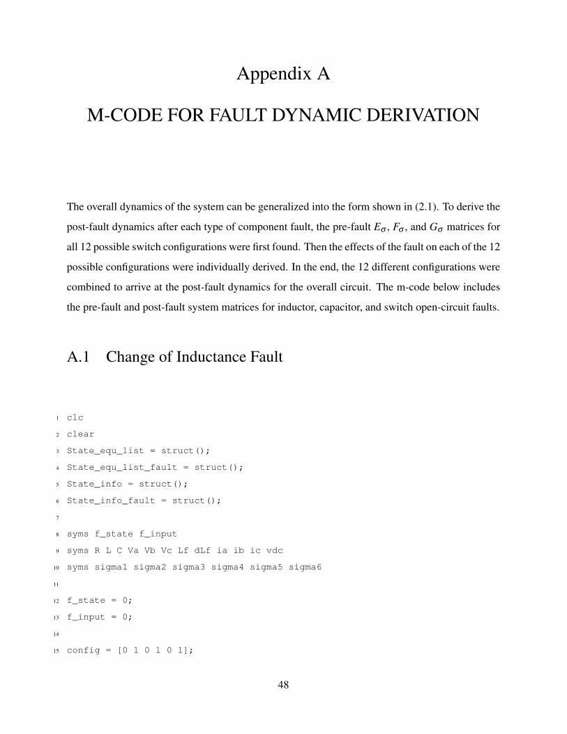
Appendix A
M-CODE FOR FAULT DYNAMIC DERIVATION
The overall dynamics of the system can be generalized into the form shown in (2.1). To derive the
post-fault dynamics after each type of component fault, the pre-fault Eσ , Fσ , and Gσ matrices for
all 12 possible switch configurations were first found. Then the effects of the fault on each of the 12
possible configurations were individually derived. In the end, the 12 different configurations were
combined to arrive at the post-fault dynamics for the overall circuit. The m-code below includes
the pre-fault and post-fault system matrices for inductor, capacitor, and switch open-circuit faults.
A.1 Change of Inductance Fault
1 clc
2 clear
3 State_equ_list = struct();
4 State_equ_list_fault = struct();
5 State_info = struct();
6 State_info_fault = struct();
7
8 syms f_state f_input
9 syms R L C Va Vb Vc Lf dLf ia ib ic vdc
10 syms sigma1 sigma2 sigma3 sigma4 sigma5 sigma6
11
12 f_state = 0;
13 f_input = 0;
14
15 config = [0 1 0 1 0 1];
48
16 state_name = ['n' num2str(config, '%d')];
17 E = [−L 0 L 0; 0 −L L 0; 1 1 1 0; 0 0 0 1]; %preafult E,A,B
18 A = [R −R 0 0; 0 R −R 0; 0 0 0 0; 0 0 0 0];
19 B = [−1 1 0; 0 −1 1; 0 0 0; 0 0 0];
20 State_info.A = E\A;
21 State_info.B = E\B;
22 State_equ_list.(state_name) = State_info;
23
24 E = [−L−Lf 0 L 0; 0 −L L 0; 1 1 1 0; 0 0 0 1]; %post−fault E, A, B
25 A = [R+dLf −R 0 0; 0 R −R 0; 0 0 0 0; 0 0 0 0];
26 B = [−1 1 0; 0 −1 1; 0 0 0; 0 0 0];
27 State_info_fault.A = E\A;
28 State_info_fault.B = E\B;
29 State_equ_list_fault.(state_name) = State_info_fault;
30
31 config = [1 0 0 1 1 0];
32 state_name = ['n' num2str(config, '%d')];
33 E = [L −L 0 0; 0 −L L 0; 1 1 1 0;0 0 0 1]; %preafult E,A,B
34 A = [−R R 0 −1; 0 R −R −1; 0 0 0 0; 0 −1/C 0 0];
35 B = [1 −1 0; 0 −1 1; 0 0 0; 0 0 0];
36 State_info.A = E\A;
37 State_info.B = E\B;
38 State_equ_list.(state_name) = State_info;
39
40 E = [L+Lf −L 0 0; 0 −L L 0; 1 1 1 0;0 0 0 1]; %post−fault E, A, B
41 A = [−R−dLf R 0 −1; 0 R −R −1; 0 0 0 0; 0 −1/C 0 0];
42 B = [1 −1 0; 0 −1 1; 0 0 0; 0 0 0];
43 State_info_fault.A = E\A;
44 State_info_fault.B = E\B;
45 State_equ_list_fault.(state_name) = State_info_fault;
46
47 config = [1 0 1 0 0 1];
48 state_name = ['n' num2str(config, '%d')];
49 E = [L 0 −L 0; 0 L −L 0; 1 1 1 0; 0 0 0 1]; %preafult E,A,B
50 A = [−R 0 R −1; 0 −R R −1; 0 0 0 0; 0 0 −1/C 0];
51 B = [1 0 −1; 0 1 −1; 0 0 0; 0 0 0];
49
52 State_info.A = E\A;
53 State_info.B = E\B;
54 State_equ_list.(state_name) = State_info;
55
56 E = [L+Lf 0 −L 0; 0 L −L 0; 1 1 1 0; 0 0 0 1]; %post−fault E, A, B
57 A = [−R−dLf 0 R −1; 0 −R R −1; 0 0 0 0; 0 0 −1/C 0];
58 B = [1 0 −1; 0 1 −1; 0 0 0; 0 0 0];
59 State_info_fault.A = E\A;
60 State_info_fault.B = E\B;
61 State_equ_list_fault.(state_name) = State_info_fault;
62
63 config = [0 1 1 0 1 0];
64 state_name = ['n' num2str(config, '%d')];
65 E = [−L L 0 0; −L 0 L 0; 1 1 1 0; 0 0 0 1]; %preafult E,A,B
66 A = [R −R 0 −1; R 0 −R −1; 0 0 0 0; −1/C 0 0 0];
67 B = [−1 1 0; −1 0 1; 0 0 0; 0 0 0];
68 State_info.A = E\A;
69 State_info.B = E\B;
70 State_equ_list.(state_name) = State_info;
71
72 E = [−L−Lf L 0 0; −L−Lf 0 L 0; 1 1 1 0; 0 0 0 1]; %post−fault E, A, B
73 A = [R+dLf −R 0 −1; R+dLf 0 −R −1; 0 0 0 0; −1/C 0 0 0];
74 B = [−1 1 0; −1 0 1; 0 0 0; 0 0 0];
75 State_info_fault.A = E\A;
76 State_info_fault.B = E\B;
77 State_equ_list_fault.(state_name) = State_info_fault;
78
79 config = [1 0 0 1 0 1];
80 state_name = ['n' num2str(config, '%d')];
81 E = [L −L 0 0; L 0 −L 0; 1 1 1 0; 0 0 0 1]; %preafult E,A,B
82 A = [−R R 0 −1; −R 0 R −1; 0 0 0 0; 1/C 0 0 0];
83 B = [1 −1 0; 1 0 −1; 0 0 0; 0 0 0];
84 State_info.A = E\A;
85 State_info.B = E\B;
86 State_equ_list.(state_name) = State_info;
87
50
88 E = [L+Lf −L 0 0; L+Lf 0 −L 0; 1 1 1 0; 0 0 0 1]; %post−fault E, A, B
89 A = [−R−dLf R 0 −1; −R−dLf 0 R −1; 0 0 0 0; 1/C 0 0 0];
90 B = [1 −1 0; 1 0 −1; 0 0 0; 0 0 0];
91 State_info_fault.A = E\A;
92 State_info_fault.B = E\B;
93 State_equ_list_fault.(state_name) = State_info_fault;
94
95 config = [0 1 1 0 0 1];
96 state_name = ['n' num2str(config, '%d')];
97 E = [−L L 0 0; 0 L −L 0; 1 1 1 0; 0 0 0 1]; %preafult E,A,B
98 A = [R −R 0 −1; 0 −R R −1; 0 0 0 0; 0 1/C 0 0];
99 B = [−1 1 0; 0 1 −1; 0 0 0; 0 0 0];
100 State_info.A = E\A;
101 State_info.B = E\B;
102 State_equ_list.(state_name) = State_info;
103
104 E = [−L−Lf L 0 0; 0 L −L 0; 1 1 1 0; 0 0 0 1]; %post−fault E, A, B
105 A = [R+dLf −R 0 −1; 0 −R R −1; 0 0 0 0; 0 1/C 0 0];
106 B = [−1 1 0; 0 1 −1; 0 0 0; 0 0 0];
107 State_info_fault.A = E\A;
108 State_info_fault.B = E\B;
109 State_equ_list_fault.(state_name) = State_info_fault;
110
111 config = [0 1 0 1 1 0];
112 state_name = ['n' num2str(config, '%d')];
113 E = [−L 0 L 0; 0 −L L 0; 1 1 1 0; 0 0 0 1]; %preafult E,A,B
114 A = [R 0 −R −1; 0 R −R −1; 0 0 0 0; 0 0 1/C 0];
115 B = [−1 0 1; 0 −1 1; 0 0 0; 0 0 0];
116 State_info.A = E\A;
117 State_info.B = E\B;
118 State_equ_list.(state_name) = State_info;
119
120 E = [−L−Lf 0 L 0; 0 −L L 0; 1 1 1 0; 0 0 0 1]; %post−fault E, A, B
121 A = [R+dLf 0 −R −1; 0 R −R −1; 0 0 0 0; 0 0 1/C 0];
122 B = [−1 0 1; 0 −1 1; 0 0 0; 0 0 0];
123 State_info_fault.A = E\A;
51
124 State_info_fault.B = E\B;
125 State_equ_list_fault.(state_name) = State_info_fault;
126
127 config = [1 0 1 0 1 0];
128 state_name = ['n' num2str(config, '%d')];
129 E = [−L 0 L 0; 0 −L L 0; 1 1 1 0; 0 0 0 1]; %preafult E,A,B
130 A = [R −R 0 0; 0 R −R 0; 0 0 0 0; 0 0 0 0];
131 B = [−1 1 0; 0 −1 1; 0 0 0; 0 0 0];
132 State_info.A = E\A;
133 State_info.B = E\B;
134 State_equ_list.(state_name) = State_info;
135
136 E = [−L−Lf 0 L 0; 0 −L L 0; 1 1 1 0; 0 0 0 1]; %post−fault E, A, B
137 A = [R+dLf −R 0 0; 0 R −R 0; 0 0 0 0; 0 0 0 0];
138 B = [−1 1 0; 0 −1 1; 0 0 0; 0 0 0];
139 State_info_fault.A = E\A;
140 State_info_fault.B = E\B;
141 State_equ_list_fault.(state_name) = State_info_fault;
142
143 names = fieldnames(State_equ_list);
144 names2 = fieldnames(State_equ_list_fault);
145 for index = 1:length(names)
146 namesindex
147 State_equ_info = State_equ_list.(namesindex);
148 State_equ_info_fault = State_equ_list_fault.(names2index);
149 dA = simplify(State_equ_info_fault.A−State_equ_info.A)*[ia ib ic vdc]'
150
151 end
A.2 Change of Capacitance Fault
1 clc
2 State_equ_list = struct();
3 State_equ_list_fault = struct();
52
4 State_info = struct();
5 State_info_fault = struct();
6
7 syms syms f_state f_input
8 syms R L C Va Vb Vc Cf dCf
9 syms ia ib ic vdc
10
11 f_state = 0;
12 f_input = 0;
13
14 config = [1 0 0 1 1 0];
15 state_name = ['n' num2str(config, '%d')];
16 E = [L −L 0 0; 0 −L L 0; 1 1 1 0;0 0 0 1];
17 A = [−R R 0 −1; 0 R −R −1; 0 0 0 0; 0 −1/C 0 0];
18 B = [1 −1 0; 0 −1 1; 0 0 0; 0 0 0];
19 State_info.A = E\A;
20 State_info.B = E\B;
21 State_equ_list.(state_name) = State_info;
22
23 E = [L −L 0 0; 0 −L L 0; 1 1 1 0;0 0 0 1];
24 A = [−R R 0 −1; 0 R −R −1; 0 0 0 0; 0 −1/(C+Cf) 0 −dCf/(C+Cf)];
25 B = [1 −1 0; 0 −1 1; 0 0 0; 0 0 0];
26 State_info_fault.A = E\A;
27 State_info_fault.B = E\B;
28 State_equ_list_fault.(state_name) = State_info_fault;
29
30 config = [1 0 1 0 0 1];
31 state_name = ['n' num2str(config, '%d')];
32 E = [L 0 −L 0; 0 L −L 0; 1 1 1 0; 0 0 0 1];
33 A = [−R 0 R −1; 0 −R R −1; 0 0 0 0; 0 0 −1/C 0];
34 B = [1 0 −1; 0 1 −1; 0 0 0; 0 0 0];
35 State_info.A = E\A;
36 State_info.B = E\B;
37 State_equ_list.(state_name) = State_info;
38
39 E = [L 0 −L 0; 0 L −L 0; 1 1 1 0; 0 0 0 1];
53
40 A = [−R 0 R −1; 0 −R R −1; 0 0 0 0; 0 0 −1/(C+Cf) −dCf/(C+Cf)];
41 B = [1 0 −1; 0 1 −1; 0 0 0; 0 0 0];
42 State_info_fault.A = E\A;
43 State_info_fault.B = E\B;
44 State_equ_list_fault.(state_name) = State_info_fault;
45
46 config = [0 1 1 0 1 0];
47 state_name = ['n' num2str(config, '%d')];
48 E = [−L L 0 0; −L 0 L 0; 1 1 1 0; 0 0 0 1];
49 A = [R −R 0 −1; R 0 −R −1; 0 0 0 0; −1/C 0 0 0];
50 B = [−1 1 0; −1 0 1; 0 0 0; 0 0 0];
51 State_info.A = E\A;
52 State_info.B = E\B;
53 State_equ_list.(state_name) = State_info;
54
55 E = [−L L 0 0; −L 0 L 0; 1 1 1 0; 0 0 0 1];
56 A = [R −R 0 −1; R 0 −R −1; 0 0 0 0; −1/(C+Cf) 0 0 −dCf/(C+Cf)];
57 B = [−1 1 0; −1 0 1; 0 0 0; 0 0 0];
58 State_info_fault.A = E\A;
59 State_info_fault.B = E\B;
60 State_equ_list_fault.(state_name) = State_info_fault;
61
62 config = [1 0 0 1 0 1];
63 state_name = ['n' num2str(config, '%d')];
64 E = [L −L 0 0; L 0 −L 0; 1 1 1 0; 0 0 0 1];
65 A = [−R R 0 −1; −R 0 R −1; 0 0 0 0; 1/C 0 0 0];
66 B = [1 −1 0; 1 0 −1; 0 0 0; 0 0 0];
67 State_info.A = E\A;
68 State_info.B = E\B;
69 State_equ_list.(state_name) = State_info;
70
71 E = [L −L 0 0; L 0 −L 0; 1 1 1 0; 0 0 0 1];
72 A = [−R R 0 −1; −R 0 R −1; 0 0 0 0; 1/(C+Cf) 0 0 −dCf/(C+Cf)];
73 B = [1 −1 0; 1 0 −1; 0 0 0; 0 0 0];
74 State_info_fault.A = E\A;
75 State_info_fault.B = E\B;
54
76 State_equ_list_fault.(state_name) = State_info_fault;
77
78 config = [0 1 1 0 0 1];
79 state_name = ['n' num2str(config, '%d')];
80 E = [−L L 0 0; 0 L −L 0; 1 1 1 0; 0 0 0 1];
81 A = [R −R 0 −1; 0 −R R −1; 0 0 0 0; 0 1/C 0 0];
82 B = [−1 1 0; 0 1 −1; 0 0 0; 0 0 0];
83 State_info.A = E\A;
84 State_info.B = E\B;
85 State_equ_list.(state_name) = State_info;
86
87 E = [−L L 0 0; 0 L −L 0; 1 1 1 0; 0 0 0 1];
88 A = [R −R 0 −1; 0 −R R −1; 0 0 0 0; 0 1/(C+Cf) 0 −dCf/(C+Cf)];
89 B = [−1 1 0; 0 1 −1; 0 0 0; 0 0 0];
90 State_info_fault.A = E\A;
91 State_info_fault.B = E\B;
92 State_equ_list_fault.(state_name) = State_info_fault;
93
94 config = [0 1 0 1 1 0];
95 state_name = ['n' num2str(config, '%d')];
96 E = [−L 0 L 0; 0 −L L 0; 1 1 1 0; 0 0 0 1];
97 A = [R 0 −R −1; 0 R −R −1; 0 0 0 0; 0 0 1/C 0];
98 B = [−1 0 1; 0 −1 1; 0 0 0; 0 0 0];
99 State_info.A = E\A;
100 State_info.B = E\B;
101 State_equ_list.(state_name) = State_info;
102
103 E = [−L 0 L 0; 0 −L L 0; 1 1 1 0; 0 0 0 1];
104 A = [R 0 −R −1; 0 R −R −1; 0 0 0 0; 0 0 1/(C+Cf) −dCf/(C+Cf)];
105 B = [−1 0 1; 0 −1 1; 0 0 0; 0 0 0];
106 State_info_fault.A = E\A;
107 State_info_fault.B = E\B;
108 State_equ_list_fault.(state_name) = State_info_fault;
109
110 names = fieldnames(State_equ_list);
111 names2 = fieldnames(State_equ_list_fault);
55
112 for index = 1:length(names)
113 namesindex
114 State_equ_info = State_equ_list.(namesindex);
115 State_equ_info_fault = State_equ_list_fault.(names2index);
116 A1 = State_equ_info.A;
117 A2 = State_equ_info_fault.A;
118 dA = simplify((State_equ_info_fault.A−State_equ_info.A)*[ia ib ic vdc]')
119
120 end
A.3 Switch 1 Open Circuit Fault
1 clear
2 clc
3 State_equ_list = struct();
4 State_equ_list_fault = struct();
5 State_info = struct();
6 State_info_fault = struct();
7
8 syms f_state f_input
9 syms R L C Va Vb Vc Rf
10 syms sigma1 sigma2 sigma3 sigma4 sigma5 sigma6
11 syms ia ib ic vdc
12
13 f_state = 0;
14 f_input = 0;
15
16 %fault config
17 config = [1 0 0 1 1 0];
18 state_name = ['n' num2str(config, '%d')];
19 E = [L −L 0 0; 0 −L L 0; 1 1 1 0;0 0 0 1];
20 A = [−R R 0 −1; 0 R −R −1; 0 0 0 0; 0 −1/C 0 0];
21 B = [1 −1 0; 0 −1 1; 0 0 0; 0 0 0];
22 State_info.A = E\A;
56
23 State_info.B = E\B;
24 State_equ_list.(state_name) = State_info;
25
26 E = [1 0 0 0; 0 −L L 0; 1 1 1 0;0 0 0 1];
27 A = [0 0 0 0; 0 R −R −1; 0 0 0 0; 0 −1/C 0 0];
28 B = [0 0 0; 0 −1 1; 0 0 0; 0 0 0];
29 State_info_fault.A = E\A;
30 State_info_fault.B = E\B;
31 State_equ_list_fault.(state_name) = State_info_fault;
32
33 %fault config
34 config = [1 0 1 0 0 1];
35 state_name = ['n' num2str(config, '%d')];
36 E = [L 0 −L 0; 0 L −L 0; 1 1 1 0; 0 0 0 1];
37 A = [−R 0 R −1; 0 −R R −1; 0 0 0 0; 0 0 −1/C 0];
38 B = [1 0 −1; 0 1 −1; 0 0 0; 0 0 0];
39 State_info.A = E\A;
40 State_info.B = E\B;
41 State_equ_list.(state_name) = State_info;
42
43 E = [1 0 0 0; 0 L −L 0; 1 1 1 0; 0 0 0 1];
44 A = [0 0 0 0; 0 −R R −1; 0 0 0 0; 0 0 −1/C 0];
45 B = [0 0 0; 0 1 −1; 0 0 0; 0 0 0];
46 State_info_fault.A = E\A;
47 State_info_fault.B = E\B;
48 State_equ_list_fault.(state_name) = State_info_fault;
49
50 config = [0 1 1 0 1 0];
51 state_name = ['n' num2str(config, '%d')];
52 E = [−L L 0 0; −L 0 L 0; 1 1 1 0; 0 0 0 1];
53 A = [R −R 0 −1; R 0 −R −1; 0 0 0 0; −1/C 0 0 0];
54 B = [−1 1 0; −1 0 1; 0 0 0; 0 0 0];
55 State_info.A = E\A;
56 State_info.B = E\B;
57 State_equ_list.(state_name) = State_info;
58
57
59 E = [−L L 0 0; −L 0 L 0; 1 1 1 0; 0 0 0 1];
60 A = [R −R 0 −1; R 0 −R −1; 0 0 0 0; −1/C 0 0 0];
61 B = [−1 1 0; −1 0 1; 0 0 0; 0 0 0];
62 State_info_fault.A = E\A;
63 State_info_fault.B = E\B;
64 State_equ_list_fault.(state_name) = State_info_fault;
65
66 %fault config
67 config = [1 0 0 1 0 1];
68 state_name = ['n' num2str(config, '%d')];
69 E = [L −L 0 0; L 0 −L 0; 1 1 1 0; 0 0 0 1];
70 A = [−R R 0 −1; −R 0 R −1; 0 0 0 0; 1/C 0 0 0];
71 B = [1 −1 0; 1 0 −1; 0 0 0; 0 0 0];
72 State_info.A = E\A;
73 State_info.B = E\B;
74 State_equ_list.(state_name) = State_info;
75
76 E = [1 0 0 0; 0 L −L 0; 1 1 1 0; 0 0 0 1];
77 A = [0 0 0 0; 0 −R R 0; 0 0 0 0; 1/C 0 0 0];
78 B = [0 0 0; 0 1 −1; 0 0 0; 0 0 0];
79 State_info_fault.A = E\A;
80 State_info_fault.B = E\B;
81 State_equ_list_fault.(state_name) = State_info_fault;
82
83 config = [0 1 1 0 0 1];
84 state_name = ['n' num2str(config, '%d')];
85 E = [−L L 0 0; 0 L −L 0; 1 1 1 0; 0 0 0 1];
86 A = [R −R 0 −1; 0 −R R −1; 0 0 0 0; 0 1/C 0 0];
87 B = [−1 1 0; 0 1 −1; 0 0 0; 0 0 0];
88 State_info.A = E\A;
89 State_info.B = E\B;
90 State_equ_list.(state_name) = State_info;
91
92 E = [−L L 0 0; 0 L −L 0; 1 1 1 0; 0 0 0 1];
93 A = [R −R 0 −1; 0 −R R −1; 0 0 0 0; 0 1/C 0 0];
94 B = [−1 1 0; 0 1 −1; 0 0 0; 0 0 0];
58

95 State_info_fault.A = E\A;
96 State_info_fault.B = E\B;
97 State_equ_list_fault.(state_name) = State_info_fault;
98
99 config = [0 1 0 1 1 0];
100 state_name = ['n' num2str(config, '%d')];
101 E = [−L 0 L 0; 0 −L L 0; 1 1 1 0; 0 0 0 1];
102 A = [R 0 −R −1; 0 R −R −1; 0 0 0 0; 0 0 1/C 0];
103 B = [−1 0 1; 0 −1 1; 0 0 0; 0 0 0];
104 State_info.A = E\A;
105 State_info.B = E\B;
106 State_equ_list.(state_name) = State_info;
107
108 E = [−L 0 L 0; 0 −L L 0; 1 1 1 0; 0 0 0 1];
109 A = [R 0 −R −1; 0 R −R −1; 0 0 0 0; 0 0 1/C 0];
110 B = [−1 0 1; 0 −1 1; 0 0 0; 0 0 0];
111 State_info_fault.A = E\A;
112 State_info_fault.B = E\B;
113 State_equ_list_fault.(state_name) = State_info_fault;
114
115 %fault config
116 config = [1 0 1 0 1 0];
117 state_name = ['n' num2str(config, '%d')];
118 E = [−L L 0 0; 0 −L L 0; 1 1 1 0; 0 0 0 1];
119 A = [R −R 0 0; 0 R −R 0; 0 0 0 0; 0 0 0 0];
120 B = [−1 1 0; 0 −1 1; 0 0 0; 0 0 0];
121 State_info.A = E\A;
122 State_info.B = E\B;
123 State_equ_list.(state_name) = State_info;
124
125 E = [1 0 0 0; 0 −L L 0; 1 1 1 0; 0 0 0 1];
126 A = [0 0 0 0; 0 R −R 0; 0 0 0 0; 0 0 0 0];
127 B = [0 0 0; 0 −1 1; 0 0 0; 0 0 0];
128 State_info_fault.A = E\A;
129 State_info_fault.B = E\B;
130 State_equ_list_fault.(state_name) = State_info_fault;
59
131
132 names = fieldnames(State_equ_list);
133 names2 = fieldnames(State_equ_list_fault);
134 for index = 1:length(names)
135 namesindex
136 State_equ_info = State_equ_list.(namesindex);
137 State_equ_info_fault = State_equ_list_fault.(names2index);
138 %A1 = State_equ_info.A
139 %A2 = State_equ_info_fault.A
140 dA = simplify(State_equ_info_fault.A−State_equ_info.A)*[ia ib ic vdc]'
141 end
60

Appendix B
SIMULATION MODELS
B.1 RL Load Inverter Simulation Model
switching signals
pulses
const
0
state3_out
state_error
state2_out
state1_out
sim_time
Switch
>= 1
Subsystem2
In1
In2
In3
In4
In5
In6
Out1
Out2
Out3
Selector
Scope3
Scope2Routing
In1
In2
Out1
Out2
Out3
Rate Transition3
Rate Transition2
Rate Transition1
Rate Transition
K1-3 calc
Out1
Out2
Out3
Goto9
K1
K6
K5
K4
I_b
I_a
V_c
V_dc
I_c
state3
state2
V_b
state1
Goto18
K3
Goto17
K2
V_a
S6
S5
S4
S3
S2
S1
Fcn
f(u)
K Ts
z-1D3 calc1
Out1
Out2
Out3
D2 calc
Out1
Out2
Out3
D1 calc
Out1
Out2
Out3
Clock
Circuit
states
pulse
v_ll
PLECSCircuit
Add
i_p
Figure B.1: Inverter with RL load and fault detection filter Simulink model
61
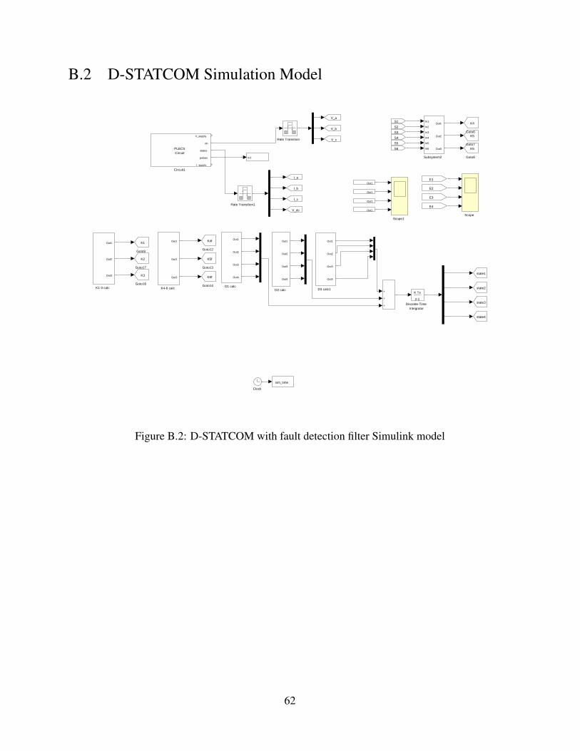
B.2 D-STATCOM Simulation Model
sim_time
Out1
Out1
Out1
Subsystem2
In1
In2
In3
In4
In5
In6
Out1
Out2
Out3
Out1
In1
Scope1Scope
Rate Transition1
Rate Transition
K4-6 calc
Out1
Out2
Out3
K1-3 calc
Out1
Out2
Out3
Goto9
K1
Goto8
K6Goto7
K5Goto6
K4
I_b
I_a
V_c
V_dc
I_c
state4
state3
state2
V_b
state1
Goto18
K3
Goto17
K2
Goto14
K6f
Goto13
K5f
Goto12
K4f
V_a
E4
E3
E2
S6
S5
S4
S3
E1
S2
S1
Discrete-TimeIntegrator
K Ts
z-1
D3 calc1
Out1
Out2
Out3
Out4
D2 calc
Out1
Out2
Out3
Out4
D1 calc
Out1
Out2
Out3
Out4
Clock
Circuit1
V_supply
vin
states
pulses
I_supply
PLECSCircuit
Figure B.2: D-STATCOM with fault detection filter Simulink model
62