1 semiconductors integrated circuits (ics). 2 semiconductors integrated circuits originally referred...
TRANSCRIPT
1
SEMICONDUCTORS
Integrated Circuits (ICs)

2
SEMICONDUCTORS
Integrated circuits originally referred to as miniaturized electronic circuits consisting of transistors, diodes, resistors and capacitors are bonded to a substrate or circuit board.
This configuration is now commonly referred to as a hybrid integrated circuit.
3
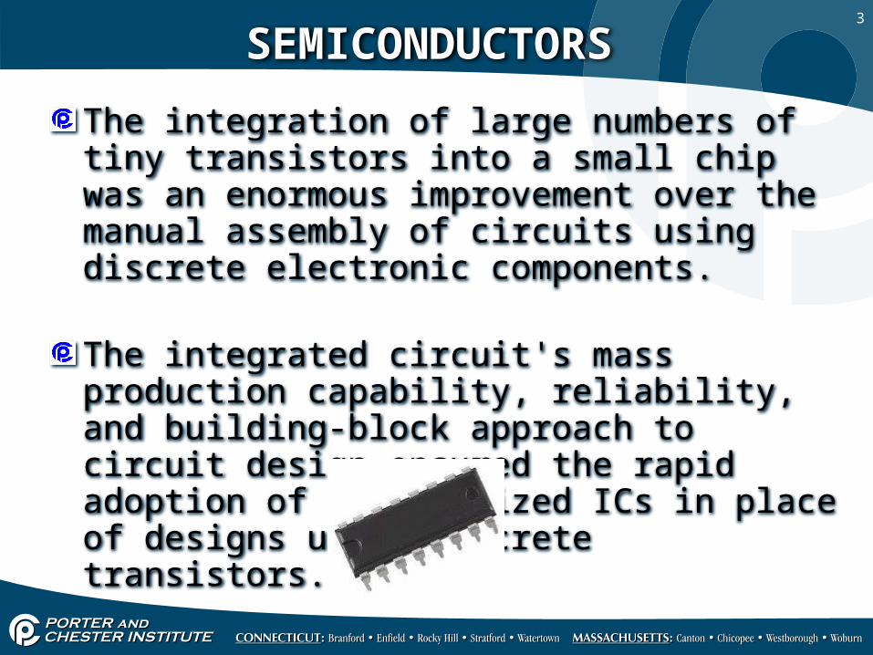
The integration of large numbers of tiny transistors into a small chip was an enormous improvement over the manual assembly of circuits using discrete electronic components.
The integrated circuit's mass production capability, reliability, and building-block approach to circuit design ensured the rapid adoption of standardized ICs in place of designs using discrete transistors.
SEMICONDUCTORS

4
Only a half century after their development was initiated, integrated circuits have become ubiquitous.
Computers, cellular phones, and other digital appliances are now inextricable parts of the structure of modern societies.
Modern computing, communications, manufacturing and transport systems, including the Internet, all depend on the existence of integrated circuits.
SEMICONDUCTORS

5
Many scholars believe that the digital revolution brought about by the microchip revolution was one of the most significant occurrences in the history of humankind.
There are several main advantages of ICs over discrete circuits:
1) SIZE2) RELIABILITY3) COST4) PERFORMANCE
SEMICONDUCTORS
6
SEMICONDUCTORS
Because of the small size of ICs they consume less power, generate less heat and operate at higher speeds.
ICs are also more reliable because they contain solid state components that are permanently connected with thin layers of metal, not soldered.
All of the components in an IC are simultaneously formed so there is less chance of making mistakes during the assembly process.
7
SEMICONDUCTORS
Cost is low because the chips, with all their components, are printed as a unit by photolithography and not constructed one transistor at a time.
Equipment that utilizes ICs will have a fewer number of parts which results in less wiring and less assembly.
Performance is high since the components switch quickly and consume little power, because the components are small and close together.

8
SEMICONDUCTORS
Performance is also enhanced by the stringent test requirements of ICs, the IC is 30 to 50 times more reliable than conventional circuitry.
As of 2006, chip areas range from a few square mm to around 350 mm, with up to 1 million transistors per mm squared.
THIS RULER IS A LITTLE BIT LARGER THAN TRUE SCALE
9
SEMICONDUCTORS
There are some disadvantages to ICs:
1. CAN’T HANDLE HIGH CURRENTS2. CAN’T HANDLE HIGH VOLTAGES3. LIMITED TO ONLY 4 COMPONENTS4. CAN’T BE REPAIRED

10
SEMICONDUCTORS
High current generates heat that can easily damage tiny components.
High voltages can break down the insulation between components and the IC because the components are very close together.
There are only four components that can be constructed within the IC; transistors, diodes, capacitors and resistors.
11
SEMICONDUCTORS
Transistors and diodes are the easiest to construct in an IC, however capacitors and resistors take up more room especially as their values increase.
Integrated circuits can’t be repaired because their internal components can’t be separated.

12
SEMICONDUCTORS
There are four types of integrated circuits:
1. Monolithic (Bipolar and MOS ICs)2. Thin film3. Thick film4. Hybrid

13
SEMICONDUCTORS
Monolithic ICs are constructed using a circular semiconductor wafer, (silicon) that is very thin and referred to as a substrate.
All of the ICs on wafer consist of the same type and number of components.
14
SEMICONDUCTORS
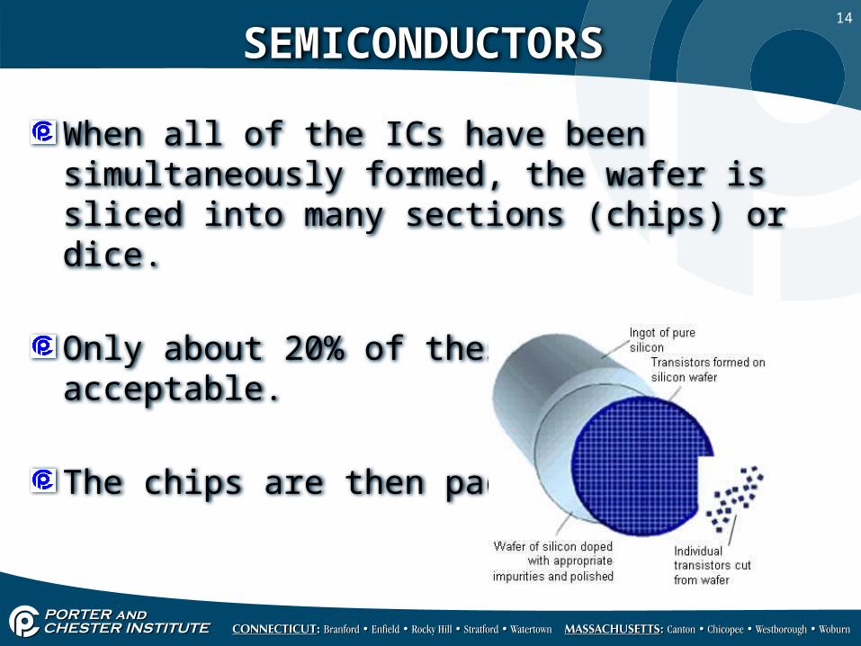
When all of the ICs have been simultaneously formed, the wafer is sliced into many sections (chips) or dice.
Only about 20% of these chips are acceptable.
The chips are then packaged.

15
SEMICONDUCTORS
The components used in Bipolar ICs are formed using the diffusion process and impurities are diffused into selected regions of a semiconductor wafer to produce PN junctions at specified locations.

16
SEMICONDUCTORS
In general ICs are classified by the number of components they contain:
SSI- Small scale integration, 200 or less components
MSI- Medium scale integration, 200 to 1000 components
LSI- Large scale integration, over 1000 components
17
SEMICONDUCTORS
MOS ICs consist of MOSFET transistors which can be either N channel or P channel devices.
The source and drain terminals are diffused into the substrate and will always be doped oppositely with respect to the substrate.
A typical MOSFET can be formed very close together, more so than a bipolar transistor.

18
SEMICONDUCTORS
A high degree of separation can be maintained between components in MOS ICs and the gate is completely isolated by the oxide coating and the source and drain regions are isolated by the PN junctions.
A MOSFET can also be used as a resistor when it is properly biased.

19
SEMICONDUCTORS
The resistance of the channel that is formed between the source and drain terminals can be adjusted by regulating its operating voltages.
MOS ICs because of their higher component density are suitable for use in MSI and LSI circuits.
20
SEMICONDUCTORS
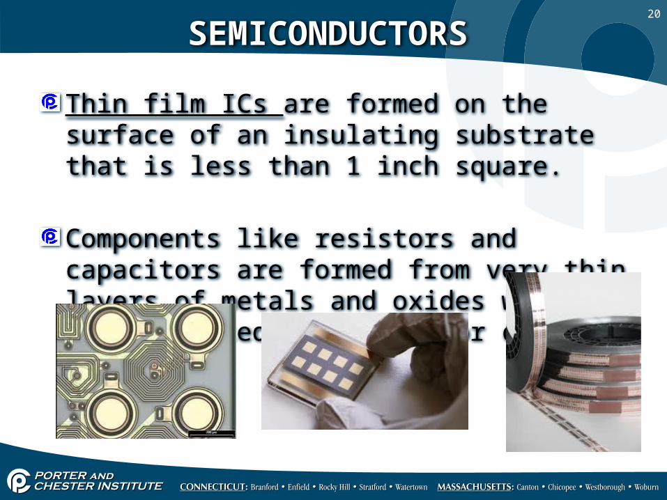
Thin film ICs are formed on the surface of an insulating substrate that is less than 1 inch square.
Components like resistors and capacitors are formed from very thin layers of metals and oxides which are deposited on a glass or ceramic substrate
21
SEMICONDUCTORS
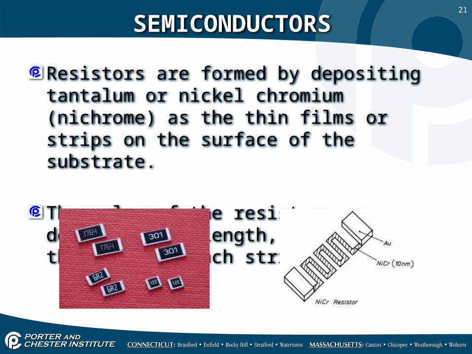
Resistors are formed by depositing tantalum or nickel chromium (nichrome) as the thin films or strips on the surface of the substrate.
The value of the resistors are determined by length, width and thickness of each strip.
22
SEMICONDUCTORS
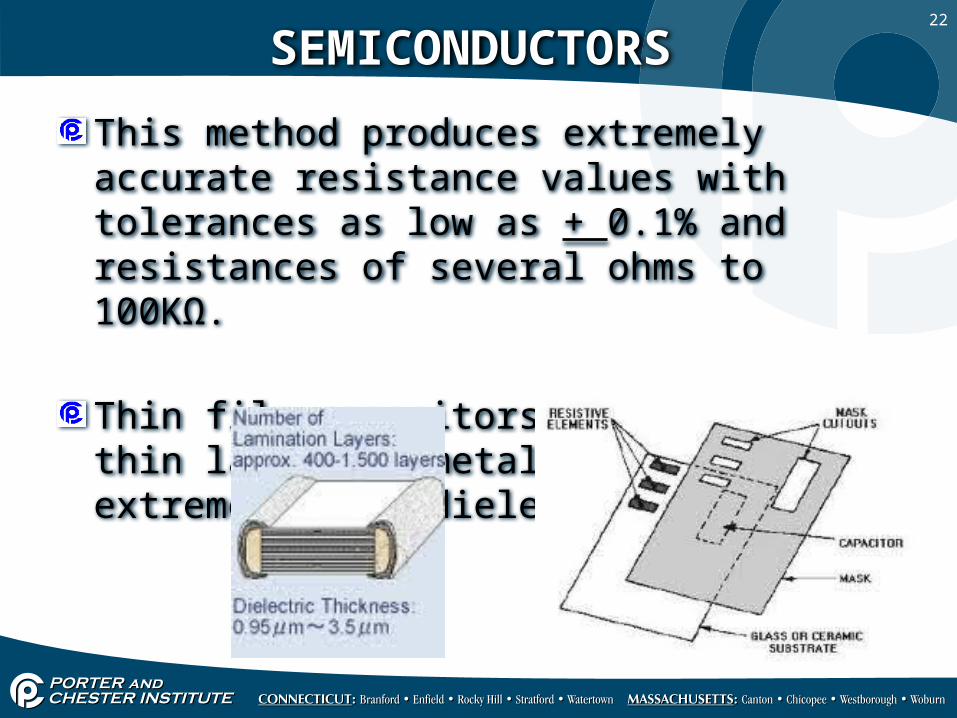
This method produces extremely accurate resistance values with tolerances as low as + 0.1% and resistances of several ohms to 100KΩ.
Thin film capacitors consist of two thin layers of metal separated by an extremely thin dielectric layer.

23
SEMICONDUCTORS
Diodes and transistors are produced separately using the monolithic technique and are formed by diffusion and then are permanently mounted on the thin film substrate and electrically connected using extremely thin wires.
24
SEMICONDUCTORS
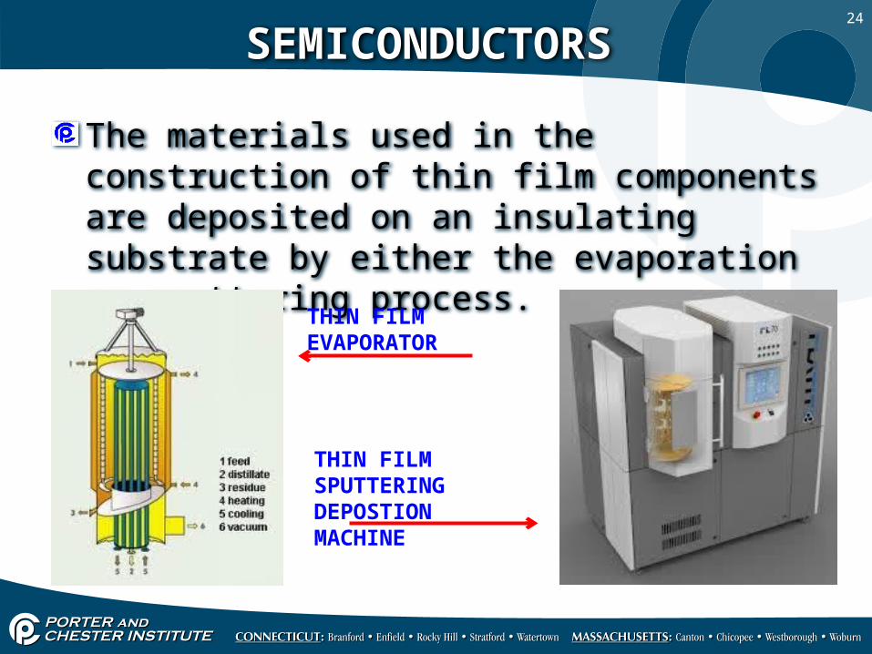
The materials used in the construction of thin film components are deposited on an insulating substrate by either the evaporation or sputtering process.
THIN FILM EVAPORATOR
THIN FILM SPUTTERING DEPOSTION MACHINE

25
SEMICONDUCTORS
Thick film ICs are formed on an insulating substrate by using a silk screen process.
A very fine wire screen is placed over the substrate and a metalized ink is forced through the screen with a squeegee, only certain portions are open allowing the ink to penetrate specific portions of the substrate

26
SEMICONDUCTORS
Diodes and transistors are formed separately as semiconductor devices and then added to the substrate.
Resistors using this process can provide tolerances as low as + 0.5% and can range from 5 to 100MΩ.

27
SEMICONDUCTORS
Hybrid ICs are formed by utilizing various combinations of monolithic, thin film and thick film techniques.

28
SEMICONDUCTORS
The hybrid approach allows a high degree of circuit complexity with the advantage of extremely accurate component values and tolerances.
It can be cheaper to utilize hybrid ICs instead of monolithic ICs.
Since hybrid circuits use discrete components as well as monolithic and film circuits, they are larger and heavier than monolithic and less reliable.