17-2017 adq7dc datasheet€¢ high-speed rf data recording • time-of-flight • scientific...
TRANSCRIPT

ADQ7 Datasheet17-2017-PA2 2017-10-17
PRELIMINARY 1(28)
ADQ7 Datasheet
ADQ7 is a high-end 14b data acquisition platform, designed to meet the most challenging measurement situations. ADQ7 features:
1 and 2 channels operations
10 GSPS, or 5 GSPS per channel
5 GByte/s sustained data transfer rate
Open FPGA for real-time DSP
Pulse detection firmware option
Software defined radio firmware option
Copyright CERN
SWEDEN | Signal Processing Devices Sweden AB | Teknikringen 6, SE-583 30 Linköping | Phone: +46 (0) 13 4650600 | Fax: +46 (0) 13 991 3044
SWITZERLAND | Signal Processing Devices | 275, Route de Saint-Julien, CH-1258 Perly, Geneva | Phone: +41 78 845 5657
US | Signal Processing Devices Inc. | 2603 Camino Ramon, Suite 200, San Ramon CA 94583 | Phone: +1 415 533 1341
www.spdevices.com
ADQ7 Datasheet
PRELIMINARY
ADQ7 Datasheet
Features Applications
• 1 or 2 analog channels
• 5 to 10 GSPS sample rate per channel
• 14 bits vertical resolution
• DC-coupled with up to 2.5 GHz analog BW
• Programmable DC-offset
• Internal and external clock reference
• Internal and external clock
• Clock reference output
• Internal and external trigger
• Multi-unit synchronization
• Time-stamp for real-time operation
• 4 GBytes data memory
• 6.4 GBytes/s sustained data streaming
• Data interface PCIe / PXIe / USB3.0 / MTCA.4 / 10 GbE
ADQ7 Development Kit
• Open FPGA for custom applications
• Real-time signal processing
• RADAR
• LIDAR
• Wireless communication
• L-band direct sampling
• High-speed RF data recording
• Time-of-flight
• Scientific instruments
• Particle physics
• Semiconductor test
• ATE
• Test and measurement
• Quantum technology
Advantages
• PC interface options for optimized systems partitioning.
• Advanced analog front-end and high sample rate for meeting detector and measurement requirements.
• Real-time custom processing for partitioning of advanced systems. This optimizes cost of ownership.
• SP Devices’ design services are available for fast integration to lower time-to-market.
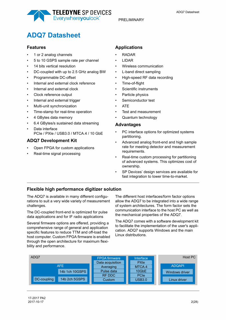
Flexible high performance digitizer solution
The ADQ7 is available in many different configu-rations to suit a very wide variety of measurement challenges.
The DC-coupled front-end is optimized for pulse data applications and for IF radio applications
Several firmware options are offered, providing a comprehensive range of general and application specific features to reduce TTM and off-load the host computer. Custom FPGA firmware is enabled through the open architecture for maximum flexi-bility and performance.
The different host interfaces/form factor options allow the ADQ7 to be integrated into a wide range of system architectures. The form factor sets the communication interface to the host PC as well as the mechanical properties of the ADQ7.
The ADQ7 comes with a software development kit to facilitate the implementation of the user's appli-cation. ADQ7 supports Windows and the main Linux distributions.
����
�'(
'")�����*$!�� +����!�� ,� �"�
����"+
-����$ ����#��
.��/0����#��
"1+�
�2������3) "
4����2
�!!�!�5/� ����
�#��!����
"/� ���!!
6'�����2��������) "
��&��/����
��)�(
"�+�
7 %8���/ �*
17-2017 PA2 2017-10-17 2(28)
ADQ7 Datasheet
PRELIMINARY
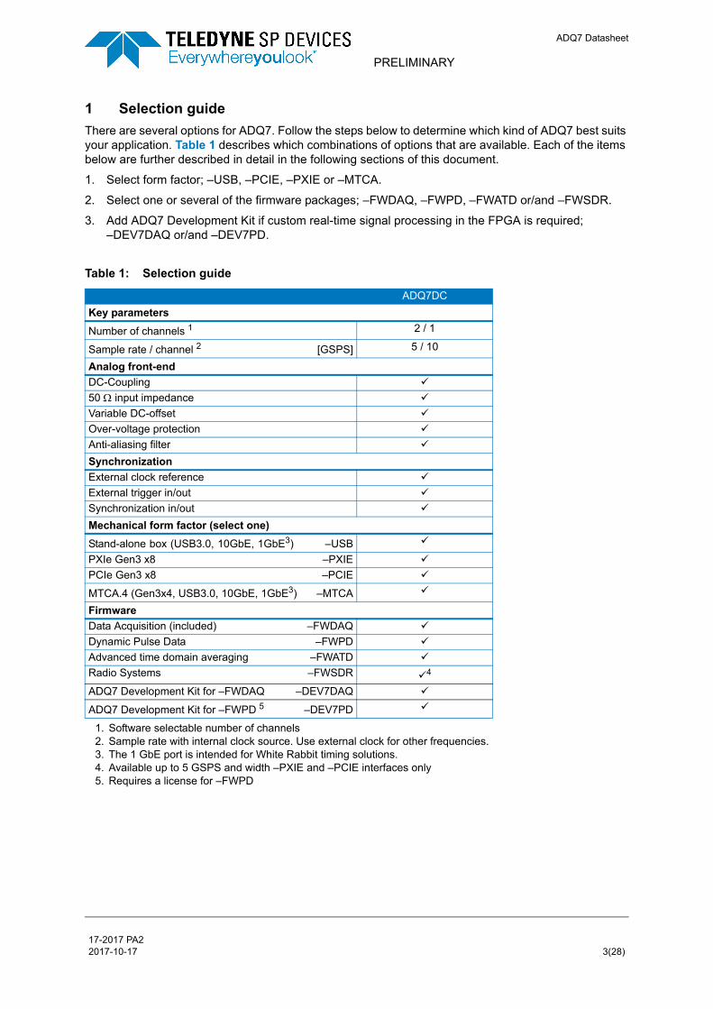
1 Selection guide
There are several options for ADQ7. Follow the steps below to determine which kind of ADQ7 best suits your application. Table 1 describes which combinations of options that are available. Each of the items below are further described in detail in the following sections of this document.
1. Select form factor; –USB, –PCIE, –PXIE or –MTCA.
2. Select one or several of the firmware packages; –FWDAQ, –FWPD, –FWATD or/and –FWSDR.
3. Add ADQ7 Development Kit if custom real-time signal processing in the FPGA is required; –DEV7DAQ or/and –DEV7PD.
Table 1: Selection guide
ADQ7DC
Key parameters
Number of channels 1
1. Software selectable number of channels
2 / 1
Sample rate / channel 2 [GSPS]
2. Sample rate with internal clock source. Use external clock for other frequencies.
5 / 10
Analog front-end
DC-Coupling
50 input impedance
Variable DC-offset
Over-voltage protection
Anti-aliasing filter
Synchronization
External clock reference
External trigger in/out
Synchronization in/out
Mechanical form factor (select one)
Stand-alone box (USB3.0, 10GbE, 1GbE3) –USB
3. The 1 GbE port is intended for White Rabbit timing solutions.
PXIe Gen3 x8 –PXIE
PCIe Gen3 x8 –PCIE
MTCA.4 (Gen3x4, USB3.0, 10GbE, 1GbE3) –MTCA
Firmware
Data Acquisition (included) –FWDAQ
Dynamic Pulse Data –FWPD
Advanced time domain averaging –FWATD
Radio Systems –FWSDR 4
4. Available up to 5 GSPS and width –PXIE and –PCIE interfaces only
ADQ7 Development Kit for –FWDAQ –DEV7DAQ
ADQ7 Development Kit for –FWPD 5 –DEV7PD
5. Requires a license for –FWPD
17-2017 PA2 2017-10-17 3(28)

ADQ7 Datasheet
PRELIMINARY
2 Preliminary technical data1
1. All values are typical unless otherwise noted.
Table 2: General parameters
ADQ7DC
Key parameters
Channels1
1. Software selectable number of channels
2 / 1
Sample rate / channel [GSPS] 5 / 10
Resolution [bits] 14
Data memory2 [GByte]
2. The data memory is shared between data (2 bytes per sample) and record head-ers.
4
Power
Power supply [V] 12
Power dissipation [W] 60
Table 3: Analog input
ADQ7DC
Analog inputs
Coupling DC
Input Impedance AC [] 50
Input Impedance DC [] 50
Input range 1 channels mode [Vpp] 1
Input range 2 channels mode [Vpp] 1
Over-voltage protection See Table 13
Bandwidth lower –3 dB [MHz] DC
Bandwidth upper –1 dB [GHz] 1.3
Bandwidth upper –3 dB [GHz] 2.5 1
1. Upper bandwidth limit is 3 GHz with digital equalizer.
Connector SMA
Variable DC-offset
Variable DC-offset range, 1 channel [V] ± 0.5
Variable DC-offset range, 2 channels [V] ±0.5
17-2017 PA2 2017-10-17 4(28)
ADQ7 Datasheet
PRELIMINARY
Table 4: Dynamic performance (TBD)
ADQ7DC
Noise density 5 GSPS, noise BW 2.5 GHz [dBFS/Hz] -151.7
Noise density 10 GSPS, noise BW 5 GHz [dBFS/Hz] -154.7
Analog performance up to 1 GHz
SNR [dB] 56
SNDR [dB] 56
SFDR [dBc] 60
ENOB [bits] 9
Analog performance up to 2.5 GHz
SNR [dB] 56
SNDR [dB] 46
SFDR [dBc] 46
ENOB [bits] 7.3
Table 5: Clock
ADQ7DC
Internal Clock Reference
Frequency [MHz] 10
Accuracy [ppm] 3 1/year
External clock reference input
Frequency [MHz] 10/100 MHz 5 ppm
Signal level (min – max) [Vpp] 0.5 – 3.3
Impedance AC [] 50
Impedance AC (high1) [] 200
Impedance DC [] 10 k
Connector SMA
MTCA.4 clock reference2
TCLKA [MHz] 10
TCLKB [MHz] 10
Clock reference output
Frequency [MHz] 10
Signal level into 50 load [Vpp] 1.2
Output impedance AC [] 50
Output impedance DC [] 10 k
Duty cycle 50% ± 5%
Connector SMA
External clock input3
Frequency [GHz] 2.5
1. Software-controlled high-impedance setting for large fan-out distribution using bussed connection.
2. Available on ADQ7 with option –MTCA.3. Sample rate in 1 channels mode is 4 x external clock frequency. Sample rate in 2
channels mode is 2 x external clock frequency.
17-2017 PA2 2017-10-17 5(28)
ADQ7 Datasheet
PRELIMINARY
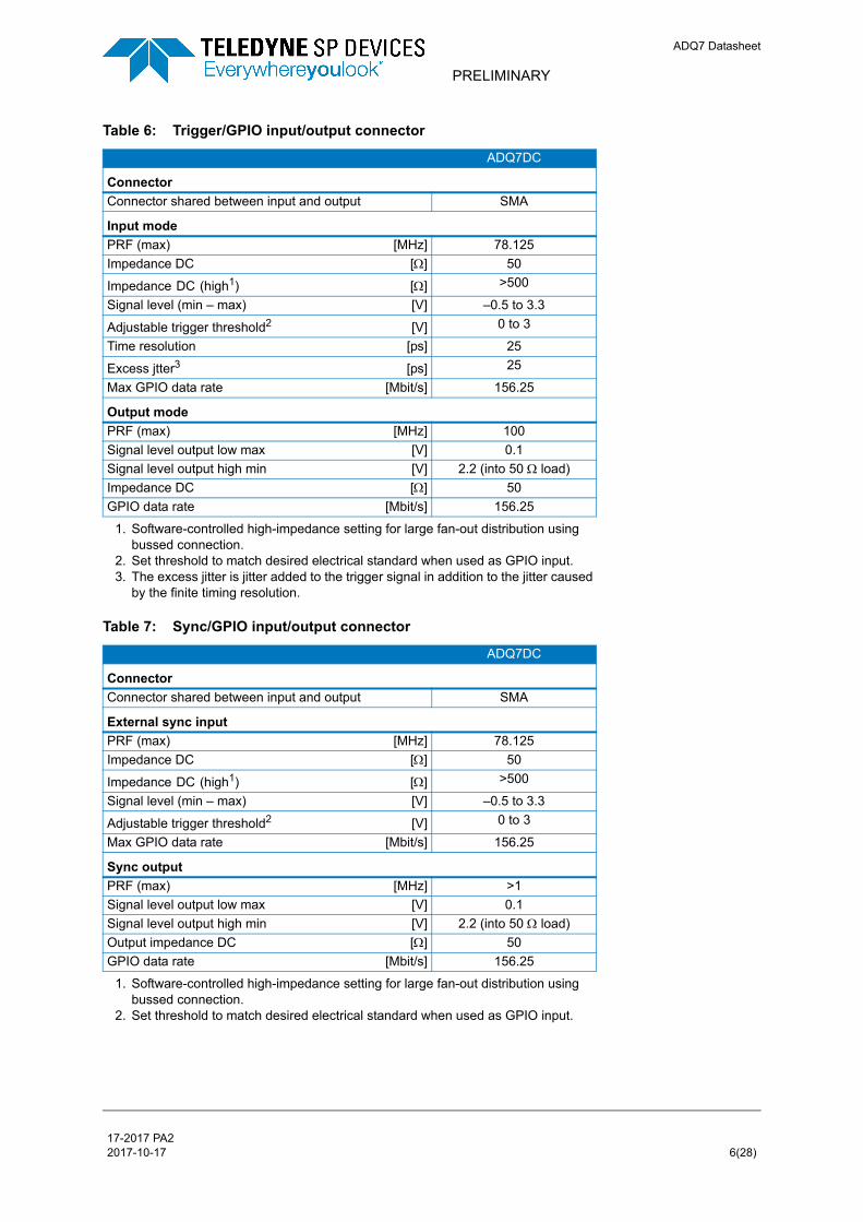
Table 6: Trigger/GPIO input/output connector
ADQ7DC
Connector
Connector shared between input and output SMA
Input mode
PRF (max) [MHz] 78.125
Impedance DC [] 50
Impedance DC (high1) [] >500
Signal level (min – max) [V] –0.5 to 3.3
Adjustable trigger threshold2 [V] 0 to 3
Time resolution [ps] 25
Excess jtter3 [ps] 25
Max GPIO data rate [Mbit/s] 156.25
Output mode
PRF (max) [MHz] 100
Signal level output low max [V] 0.1
Signal level output high min [V] 2.2 (into 50 load)
Impedance DC [] 50
GPIO data rate [Mbit/s] 156.25
1. Software-controlled high-impedance setting for large fan-out distribution using bussed connection.
2. Set threshold to match desired electrical standard when used as GPIO input.3. The excess jitter is jitter added to the trigger signal in addition to the jitter caused
by the finite timing resolution.
Table 7: Sync/GPIO input/output connector
ADQ7DC
Connector
Connector shared between input and output SMA
External sync input
PRF (max) [MHz] 78.125
Impedance DC [] 50
Impedance DC (high1) [] >500
Signal level (min – max) [V] –0.5 to 3.3
Adjustable trigger threshold2 [V] 0 to 3
Max GPIO data rate [Mbit/s] 156.25
Sync output
PRF (max) [MHz] >1
Signal level output low max [V] 0.1
Signal level output high min [V] 2.2 (into 50 load)
Output impedance DC [] 50
GPIO data rate [Mbit/s] 156.25
1. Software-controlled high-impedance setting for large fan-out distribution using bussed connection.
2. Set threshold to match desired electrical standard when used as GPIO input.
17-2017 PA2 2017-10-17 6(28)

ADQ7 Datasheet
PRELIMINARY
Table 8: GPIO
INTERFACE OPTION
–USB –PXIE –PCIE –MTCA
GPIO multiple usage
I/O SMA connector TRIG TRIG TRIG TRIG
SYNC SYNC SYNC SYNC
GPIO single ended
I/O – 12 12 –
GPIO differential LVDS
Input – 2 2 –
Clock input – 2 2 –
Output – 3 3 –
Table 9: General specifications
INTERFACE OPTION
–USB –PXIE –PCIE –MTCA
Data rate
Interface to host PC USB3.0 10 GbE PCIe PCIe PCIe
Standard USB3.0 UDP point to point
Gen3 by 8 lanes
Gen3 by 8 lanes
Gen3 by 4 lanes
Data rate peak1 [MBytes/s] 400 1250 6800 6800 3400
Data rate sustained2 [MBytes/s] 200 1000 5000 5000 2500
Mechanical
Box size [mm3] 208,3 x 217,6 x 53 – – –
Bus width mechanical [lanes] – – 16 3 8
Weight [g] 1000 700 700 800
Board width [slot] – 24 25 Double width
Board length – – full length –
Board height – 3U – Mid–size
Electrical
Power supply External6 From chassis
6-pin ATX power
From chassis
Bus width electrical [lanes] – 8 8 4
Temperature range
Operation [oC] 0 to 45 0 to 45 0 to 45 0 to 45
Compliances
CE
RoHS2
FCC Exclusion according to CFR 47, part 15, paragraph 15.103(c)
1. This is the peak capacity supported by ADQ7. The system performance is depends on the capacity of the complete system, including the host computer.
2. This is the sustained data rate supported by ADQ7, i.e. the transfer rate of data (excluding headers etc.) main-tained on average for a long time. The system performance is depends on the capacity of the complete sys-tem, including the host computer.
3. The wide contact is required to support the weight of the board. 4. 2nd slot is left of the connector. See Section 16.8. 5. 2nd slot is on the component side of the connector. 6. Use only the power supply which is included in the delivery of ADQ7–USB.
17-2017 PA2 2017-10-17 7(28)
ADQ7 Datasheet
PRELIMINARY
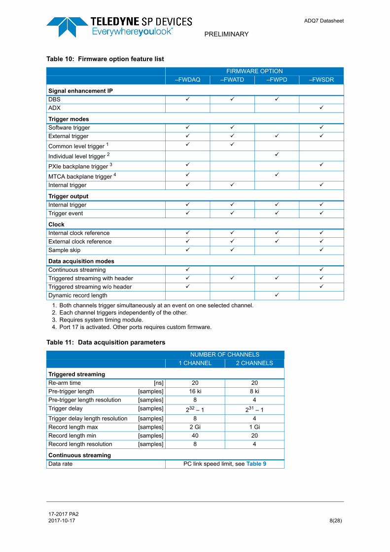
Table 10: Firmware option feature list
FIRMWARE OPTION
–FWDAQ –FWATD –FWPD –FWSDR
Signal enhancement IP
DBS
ADX
Trigger modes
Software trigger
External trigger
Common level trigger 1
Individual level trigger 2
PXIe backplane trigger 3
MTCA backplane trigger 4
Internal trigger
Trigger output
Internal trigger
Trigger event
Clock
Internal clock reference
External clock reference
Sample skip
Data acquisition modes
Continuous streaming
Triggered streaming with header
Triggered streaming w/o header
Dynamic record length
1. Both channels trigger simultaneously at an event on one selected channel.2. Each channel triggers independently of the other. 3. Requires system timing module. 4. Port 17 is activated. Other ports requires custom firmware.
Table 11: Data acquisition parameters
NUMBER OF CHANNELS
1 CHANNEL 2 CHANNELS
Triggered streaming
Re-arm time [ns] 20 20
Pre-trigger length [samples] 16 ki 8 ki
Pre-trigger length resolution [samples] 8 4
Trigger delay [samples] 232 – 1 231 – 1
Trigger delay length resolution [samples] 8 4
Record length max [samples] 2 Gi 1 Gi
Record length min [samples] 40 20
Record length resolution [samples] 8 4
Continuous streaming
Data rate PC link speed limit, see Table 9
17-2017 PA2 2017-10-17 8(28)
ADQ7 Datasheet
PRELIMINARY
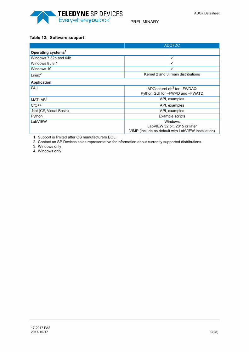
Table 12: Software support
ADQ7DC
Operating systems1
Windows 7 32b and 64b
Windows 8 / 8.1
Windows 10
Linux2 Kernel 2 and 3, main distributions
Application
GUI ADCaptureLab3 for –FWDAQ Python GUI for –FWPD and –FWATD
MATLAB4 API, examples
C/C++ API, examples
.Net (C#, Visual Basic) API, examples
Python Example scripts
LabVIEW Windows, LabVIEW 32 bit, 2015 or later
VIMP (include as default with LabVIEW installation)
1. Support is limited after OS manufacturers EOL. 2. Contact an SP Devices sales representative for information about currently supported distributions. 3. Windows only 4. Windows only
17-2017 PA2 2017-10-17 9(28)
ADQ7 Datasheet
PRELIMINARY
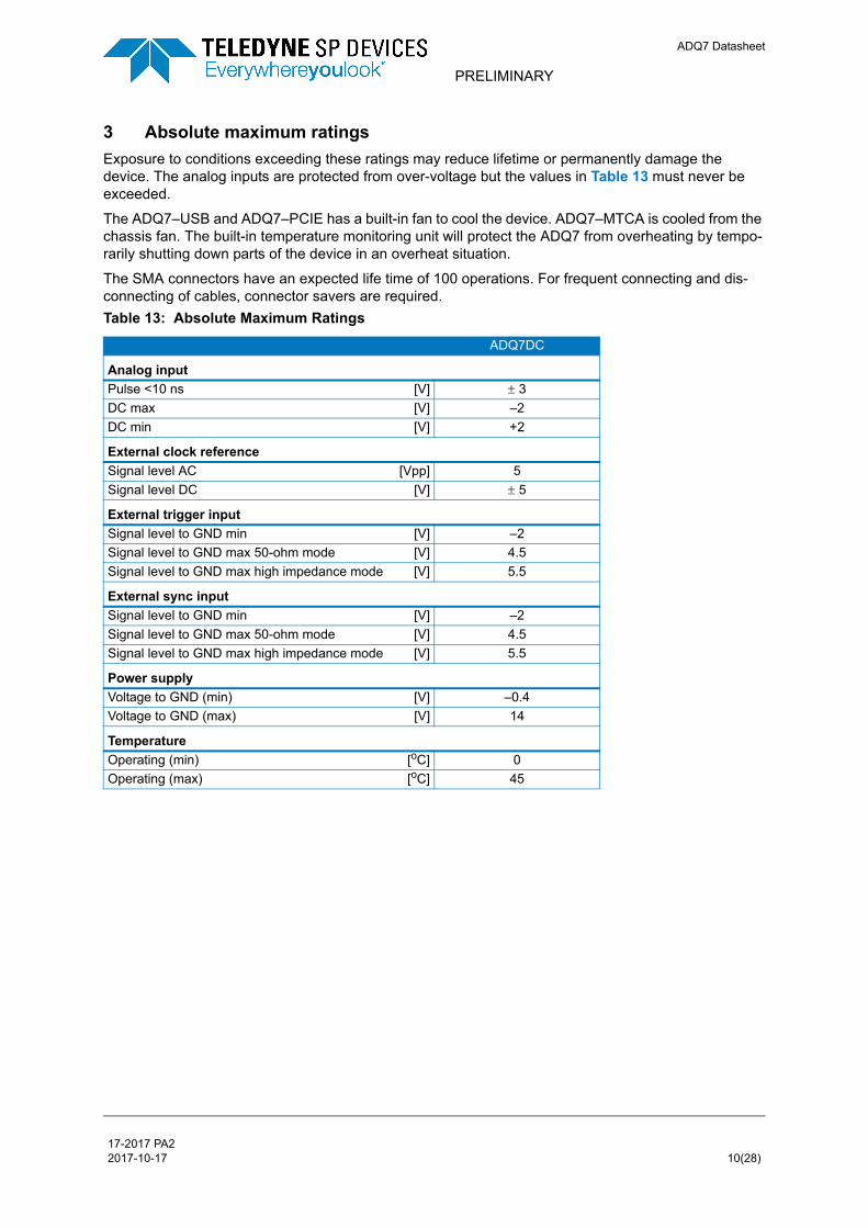
3 Absolute maximum ratings
Exposure to conditions exceeding these ratings may reduce lifetime or permanently damage the device. The analog inputs are protected from over-voltage but the values in Table 13 must never be exceeded.
The ADQ7–USB and ADQ7–PCIE has a built-in fan to cool the device. ADQ7–MTCA is cooled from the chassis fan. The built-in temperature monitoring unit will protect the ADQ7 from overheating by tempo-rarily shutting down parts of the device in an overheat situation.
The SMA connectors have an expected life time of 100 operations. For frequent connecting and dis-connecting of cables, connector savers are required.
Table 13: Absolute Maximum Ratings
ADQ7DC
Analog input
Pulse <10 ns [V] 3
DC max [V] –2
DC min [V] +2
External clock reference
Signal level AC [Vpp] 5
Signal level DC [V] 5
External trigger input
Signal level to GND min [V] –2
Signal level to GND max 50-ohm mode [V] 4.5
Signal level to GND max high impedance mode [V] 5.5
External sync input
Signal level to GND min [V] –2
Signal level to GND max 50-ohm mode [V] 4.5
Signal level to GND max high impedance mode [V] 5.5
Power supply
Voltage to GND (min) [V] –0.4
Voltage to GND (max) [V] 14
Temperature
Operating (min) [oC] 0
Operating (max) [oC] 45
17-2017 PA2 2017-10-17 10(28)

ADQ7 Datasheet
PRELIMINARY
4 Integrating the ADQ7
Figure 1 illustrates how ADQ7 supports the key parts of the system integration.
4.1 Detecting the analog signal
The analog front-end combines high dynamic range with high bandwidth to support the most advanced detectors. The DC-coupled front-end has high sensitivity to simplify the interfacing. DC-offset enable doubled resolution for uni-polar pulses.
4.2 Timing and synchronization
The clock management and trigger support con-nects with the infrastructure of the system. There are two main situations where synchronization is required; one ADQ7 to another type of equipment and several ADQ7 units in a multi-channel appli-cation.
The ADQ7 can act as master and generate timing for the entire system and thereby save additional timing cards. It can also receive trigger and clocks from other devices. Synchronization and GPIO signals allow advanced sequencing.
The methods for synchronize several units in one location according to the application note 15-1583 “ADQ14 synchronizing several units” are also valid for ADQ7. For an installation with long dis-tance between the measurement nodes, White Rabbit enables accurate timing.
4.3 Real-time signal processing
The data acquisition engine in the FPGA supports several methods for acquiring data and transfer it to the host PC. Since the data rate from the ADC is high, some parts of the application is preferably integrated into the FPGA to relax the load on the
CPU in the host computer. There is a set of appli-cation-specific firmware options available to enable efficient real-time signal processing. In addition, the FPGA is open to the user through the ADQ7 Development Kit for integration of custom algorithms.
4.4 System integration
The interface to the host PC is one important parameter in the system integration. To enable an optimal solution, the ADQ7 offers a wide variety of form factors.
Both the mechanical and electrical properties in various standards are important for the result. The mechanical properties enables an optimal place-ment of the ADQ7 inside the target system and also which type of PC to use. The different electri-cal properties of the interface determine data transfer rate and noise immunity.
4.5 Building the application
The open ADQAPI is a software package includ-ing drivers and software development kit for inte-grating the ADQ7 into an application. The many examples and application notes simplify the inte-gration process and shorten the time-to-market.
Partitioning the application between a high level analysis software in the host PC and a low level real-time data analysis in the open FPGA enables high performance applications to run on a cost-effective PC solution.
Figure 1: Integrating the ADQ7 into the system.
���� ��������
�������� ������
������
���� "�
�������
���� %����� ��
������ "!� ����"�
��������"�"�� ��������� ������ ����������� ��������
������ �����#"�����
����&������������
����$��� �����������
�����$ ����������� ��������
��&������
���
���%
�������
���
��������&����� ����$���
���� ��#������� &��
�" ��#���' ������ ���#���
�� !()
4����*
"+��
"���
7�%8��
�����$� ���#��
9��"$ ���#��
��&����� ��((��
��&�"����
17-2017 PA2 2017-10-17 11(28)
ADQ7 Datasheet
PRELIMINARY
5 Software tools
5.1 Operating systems
The software package includes drivers for the most common versions of Windows and several Linux distributions.
5.2 Software development kit, SDK
The ADQ7 digitizer is easily integrated into the application by using the software development kit, SDK. The SDK is included free of charge with the ADQ7.
The SDK includes programming examples and reference projects for several platforms. The ADQAPI reference guide describes all functions in detail.
Using the SDK enables rapid custom processing of large amounts of data and real-time control of the digitizer.
5.3 ADCaptureLab GUI
The ADQ7 is supplied with the ADCaptureLab software that provides quick and easy control of the digitizer. The tool also offers both time-domain and frequency-domain analysis, see Figure 2. Data can be saved in different file formats for off-line analysis. With ADCaptureLab, the ADQ7 operates as a bench-top oscilloscope.
Note that the GUI ADCaptureLab only represent a subset of the flexibility of the ADQ7. The full potential of the ADQ7 is reached using the SDK.
ADCaptureLab is available for Windows only.
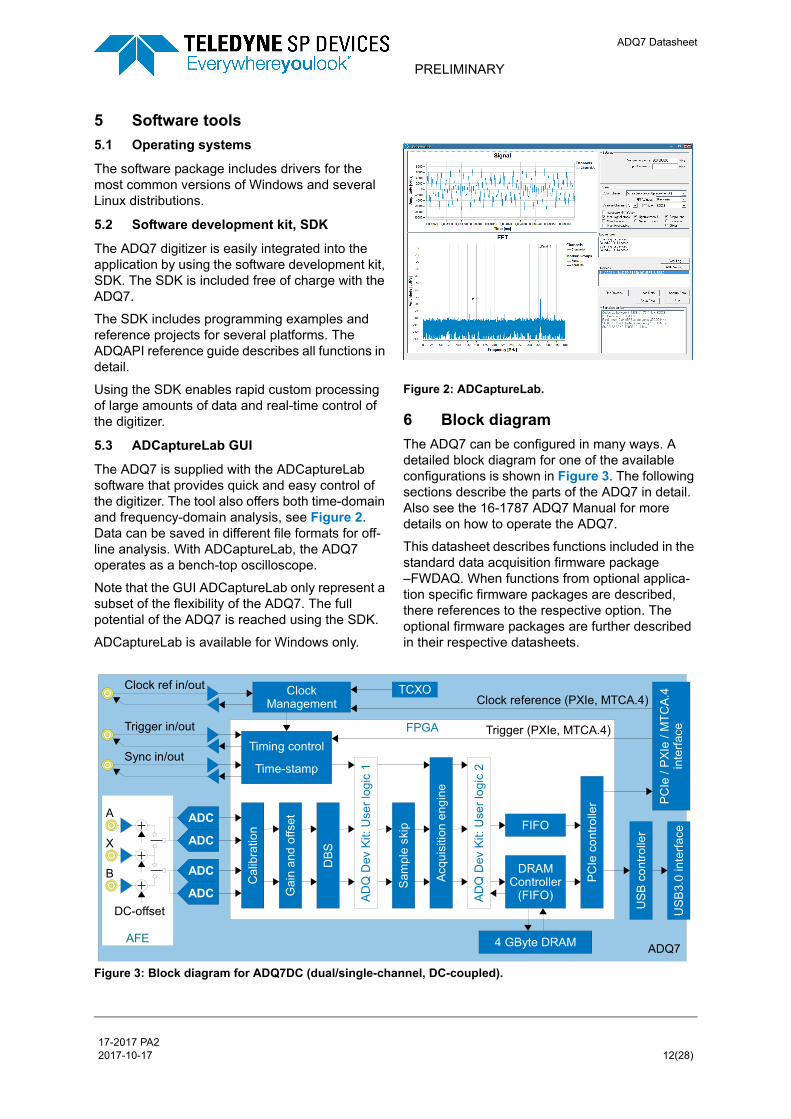
6 Block diagram
The ADQ7 can be configured in many ways. A detailed block diagram for one of the available configurations is shown in Figure 3. The following sections describe the parts of the ADQ7 in detail. Also see the 16-1787 ADQ7 Manual for more details on how to operate the ADQ7.
This datasheet describes functions included in the standard data acquisition firmware package –FWDAQ. When functions from optional applica-tion specific firmware packages are described, there references to the respective option. The optional firmware packages are further described in their respective datasheets.
Figure 2: ADCaptureLab.
Figure 3: Block diagram for ADQ7DC (dual/single-channel, DC-coupled).
����
�"��
"��������������
��������� �!
"����"�"1���"�!�����
�������
������#�$%��������
������������
��&
����������������'"1��(�!�����)�����
!��� ���
��1*
��������"�:�
� ����������
� ���� �
%������������
%��;����������
��������#�$�%���������
��<:����������
� �������
�������
���
�����
�����
�����
�����
������"�:�
�����������"�:�
� �!����������'���*)
���*
�������'"1��(�!�����)
���������
�
1
�
17-2017 PA2 2017-10-17 12(28)

ADQ7 Datasheet
PRELIMINARY
7 Analog front-end
DC-coupling (ADQ7DC)
The DC-coupled analog front-end contains overvoltage protection and software programmable DC-offset. The DC-coupled AFE also has a noise-suppression anti-aliasing filter. The DC-offset is set in 15 steps and the range is covering the full signal range. The set-tings are user controlled via software.
The overvoltage protection is crucial in pulse data systems where high voltage detectors are driving the input. The overvoltage protec-tion reduces the damage at accidental discharges. See Section 3 for absolute limits without damage.
The DC-coupled front-end is switchable between 2 channels and one channel with time interleaved sampling, which result in twice the sample rate.
Number of channels
The ADQ7DC is switchable between two channels at 5 GSPS and one channel at 10 GSPS.
����������
����
����������
�����������������
���
��������������
� ���� �� ����
���
���
���
���
������
17-2017 PA2 2017-10-17 13(28)
ADQ7 Datasheet
PRELIMINARY
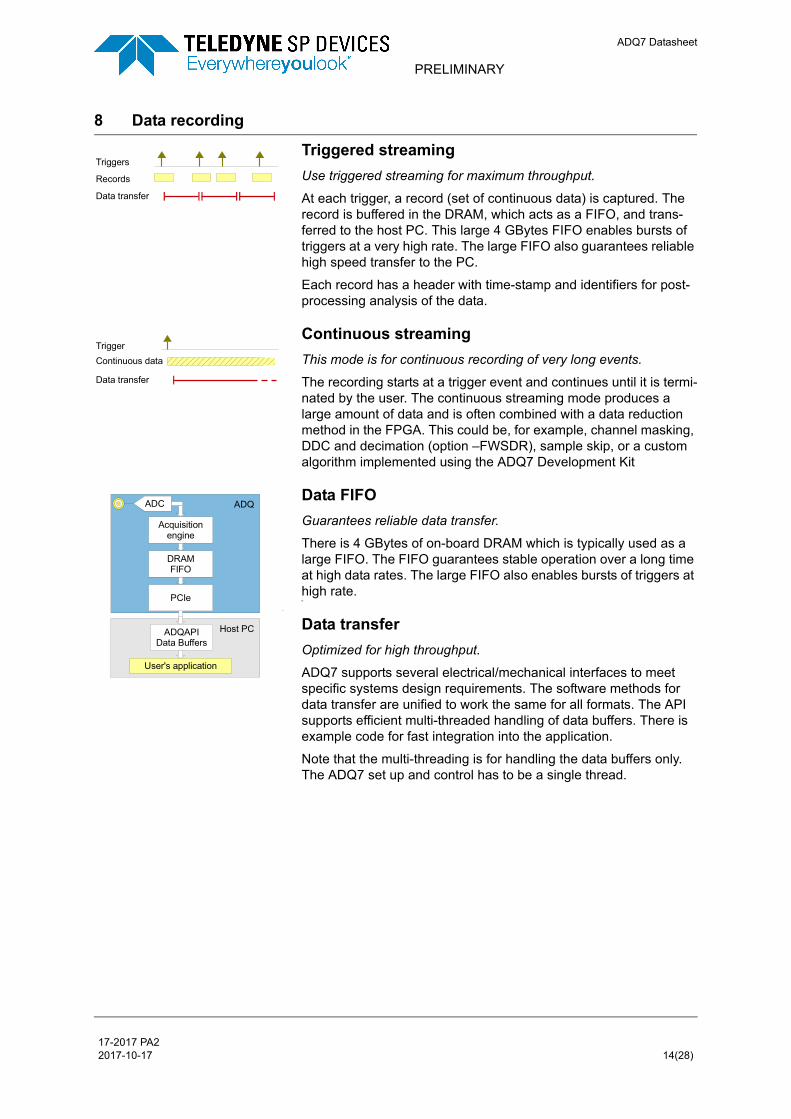
8 Data recording
Triggered streaming
Use triggered streaming for maximum throughput.
At each trigger, a record (set of continuous data) is captured. The record is buffered in the DRAM, which acts as a FIFO, and trans-ferred to the host PC. This large 4 GBytes FIFO enables bursts of triggers at a very high rate. The large FIFO also guarantees reliable high speed transfer to the PC.
Each record has a header with time-stamp and identifiers for post-processing analysis of the data.
Continuous streaming
This mode is for continuous recording of very long events.
The recording starts at a trigger event and continues until it is termi-nated by the user. The continuous streaming mode produces a large amount of data and is often combined with a data reduction method in the FPGA. This could be, for example, channel masking, DDC and decimation (option –FWSDR), sample skip, or a custom algorithm implemented using the ADQ7 Development Kit
Data FIFO
Guarantees reliable data transfer.
There is 4 GBytes of on-board DRAM which is typically used as a large FIFO. The FIFO guarantees stable operation over a long time at high data rates. The large FIFO also enables bursts of triggers at high rate. fr
Data transfer
Optimized for high throughput.
ADQ7 supports several electrical/mechanical interfaces to meet specific systems design requirements. The software methods for data transfer are unified to work the same for all formats. The API supports efficient multi-threaded handling of data buffers. There is example code for fast integration into the application.
Note that the multi-threading is for handling the data buffers only. The ADQ7 set up and control has to be a single thread.
��������
�������
��������
����������������
��
����������
������
�����
��������� �
��������
�������
���
��������� � �� �
��������
����
������� !������
���
"���#� ��$����
17-2017 PA2 2017-10-17 14(28)
ADQ7 Datasheet
PRELIMINARY
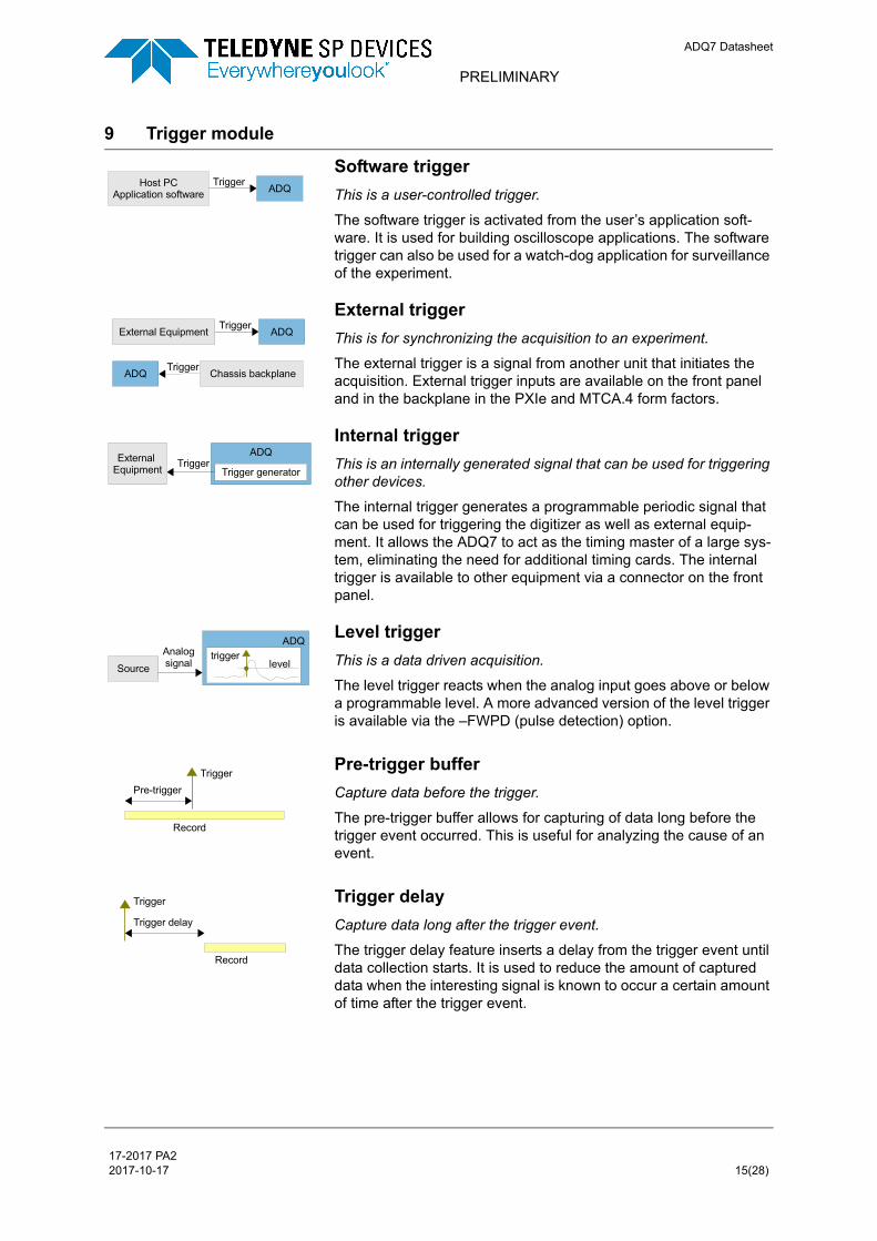
9 Trigger module
Software trigger
This is a user-controlled trigger.
The software trigger is activated from the user’s application soft-ware. It is used for building oscilloscope applications. The software trigger can also be used for a watch-dog application for surveillance of the experiment.
External trigger
This is for synchronizing the acquisition to an experiment.
The external trigger is a signal from another unit that initiates the acquisition. External trigger inputs are available on the front panel and in the backplane in the PXIe and MTCA.4 form factors.
Internal trigger
This is an internally generated signal that can be used for triggering other devices.
The internal trigger generates a programmable periodic signal that can be used for triggering the digitizer as well as external equip-ment. It allows the ADQ7 to act as the timing master of a large sys-tem, eliminating the need for additional timing cards. The internal trigger is available to other equipment via a connector on the front panel.
Level trigger
This is a data driven acquisition.
The level trigger reacts when the analog input goes above or below a programmable level. A more advanced version of the level trigger is available via the –FWPD (pulse detection) option.
Pre-trigger buffer
Capture data before the trigger.
The pre-trigger buffer allows for capturing of data long before the trigger event occurred. This is useful for analyzing the cause of an event.
Trigger delay
Capture data long after the trigger event.
The trigger delay feature inserts a delay from the trigger event until data collection starts. It is used to reduce the amount of captured data when the interesting signal is known to occur a certain amount of time after the trigger event.
���������� ����
�������� ��� ����
��������
��� �� �������������������
����������������
�������� �
����� ��� � �����
��� ���������� ��
���
������� ����� �
������ �����
������
�����������
������
�������
�����������
��� ��
17-2017 PA2 2017-10-17 15(28)
ADQ7 Datasheet
PRELIMINARY
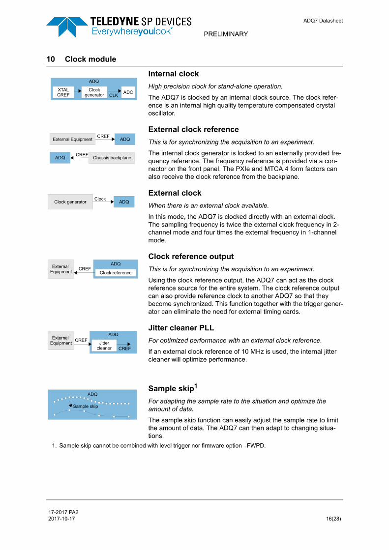
10 Clock module
Internal clock
High precision clock for stand-alone operation.
The ADQ7 is clocked by an internal clock source. The clock refer-ence is an internal high quality temperature compensated crystal oscillator.
External clock reference
This is for synchronizing the acquisition to an experiment.
The internal clock generator is locked to an externally provided fre-quency reference. The frequency reference is provided via a con-nector on the front panel. The PXIe and MTCA.4 form factors can also receive the clock reference from the backplane.
External clock
When there is an external clock available.
In this mode, the ADQ7 is clocked directly with an external clock. The sampling frequency is twice the external clock frequency in 2-channel mode and four times the external frequency in 1-channel mode.
Clock reference output
This is for synchronizing the acquisition to an experiment.
Using the clock reference output, the ADQ7 can act as the clock reference source for the entire system. The clock reference output can also provide reference clock to another ADQ7 so that they become synchronized. This function together with the trigger gener-ator can eliminate the need for external timing cards.
Jitter cleaner PLL
For optimized performance with an external clock reference.
If an external clock reference of 10 MHz is used, the internal jitter cleaner will optimize performance.
Sample skip1
For adapting the sample rate to the situation and optimize the amount of data.
The sample skip function can easily adjust the sample rate to limit the amount of data. The ADQ7 can then adapt to changing situa-tions.
1. Sample skip cannot be combined with level trigger nor firmware option –FWPD.
���
���� � ���� ���
��������
���
������
��� �� � ������������
�����������������
�����
�����������
�������
� ��������������� ���������������
���
��������������� ����
���������������
���
���������
17-2017 PA2 2017-10-17 16(28)
ADQ7 Datasheet
PRELIMINARY
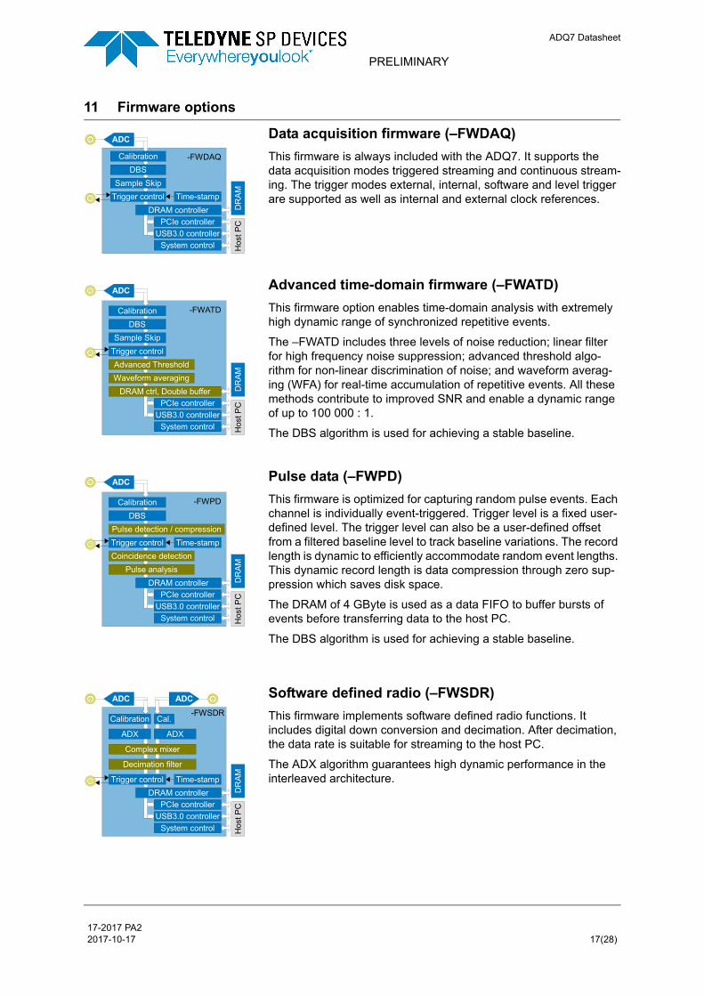
11 Firmware options
Data acquisition firmware (–FWDAQ)
This firmware is always included with the ADQ7. It supports the data acquisition modes triggered streaming and continuous stream-ing. The trigger modes external, internal, software and level trigger are supported as well as internal and external clock references.
Advanced time-domain firmware (–FWATD)
This firmware option enables time-domain analysis with extremely high dynamic range of synchronized repetitive events.
The –FWATD includes three levels of noise reduction; linear filter for high frequency noise suppression; advanced threshold algo-rithm for non-linear discrimination of noise; and waveform averag-ing (WFA) for real-time accumulation of repetitive events. All these methods contribute to improved SNR and enable a dynamic range of up to 100 000 : 1.
The DBS algorithm is used for achieving a stable baseline.
Pulse data (–FWPD)
This firmware is optimized for capturing random pulse events. Each channel is individually event-triggered. Trigger level is a fixed user-defined level. The trigger level can also be a user-defined offset from a filtered baseline level to track baseline variations. The record length is dynamic to efficiently accommodate random event lengths. This dynamic record length is data compression through zero sup-pression which saves disk space.
The DRAM of 4 GByte is used as a data FIFO to buffer bursts of events before transferring data to the host PC.
The DBS algorithm is used for achieving a stable baseline.
Software defined radio (–FWSDR)
This firmware implements software defined radio functions. It includes digital down conversion and decimation. After decimation, the data rate is suitable for streaming to the host PC.
The ADX algorithm guarantees high dynamic performance in the interleaved architecture.
������
����� ���������
����� ���������
����� � ���������
�!"��#� ������
�$#������%�
&�%''��� ������
�$�%�$�%��
(�"����
&%#�)"�$#�
���
����
�����
)�����
�����������
��������� ��� �
��������� �
��������������� ��
���� ������������
��� �����!�� "�����"����
�����
�#�
$�%��� ��� ����
&�#'�(�� ��� ����
�)������ ��� � * ���$�
���
++�
��������� ��� �
��������� �
������������ ����� ������� �
�������������
�����
� �
�!��� ��� ����
"� #�$�� ��� ����
�������� ��� � % ����
�&�'
�&�'�� ��� ����
� ����������������� �
����(�����
(�,��
������ ��� ����
�������� ��� ����
�������� ��� �
� �!�� �! �
" �����
��#�� ��� ����
$!��%�� ��
� ��
$�!&&���� ��� �
��'
����� ���
��'
� ����(��!(��
���!� �! ���!����
��#
17-2017 PA2 2017-10-17 17(28)
ADQ7 Datasheet
PRELIMINARY
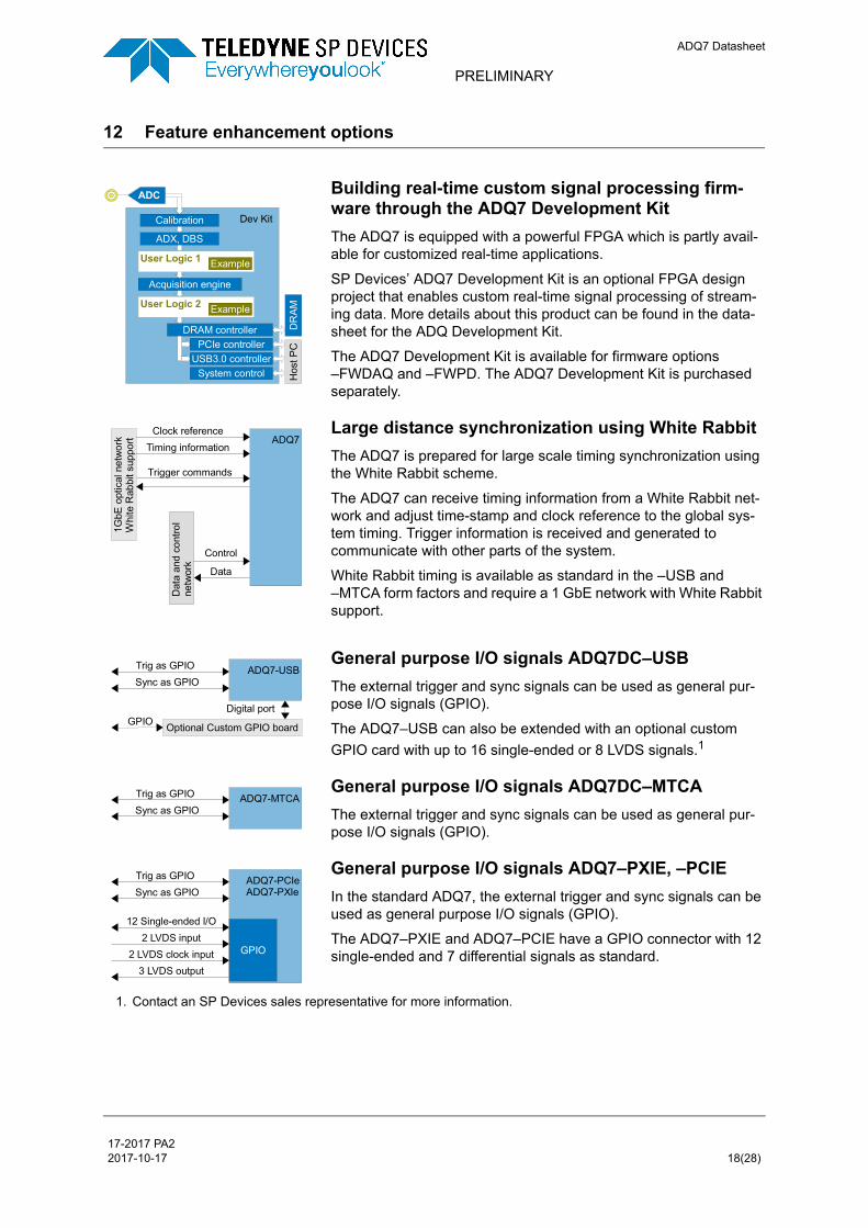
12 Feature enhancement options
Building real-time custom signal processing firm-ware through the ADQ7 Development Kit
The ADQ7 is equipped with a powerful FPGA which is partly avail-able for customized real-time applications.
SP Devices’ ADQ7 Development Kit is an optional FPGA design project that enables custom real-time signal processing of stream-ing data. More details about this product can be found in the data-sheet for the ADQ Development Kit.
The ADQ7 Development Kit is available for firmware options –FWDAQ and –FWPD. The ADQ7 Development Kit is purchased separately.
Large distance synchronization using White Rabbit
The ADQ7 is prepared for large scale timing synchronization using the White Rabbit scheme.
The ADQ7 can receive timing information from a White Rabbit net-work and adjust time-stamp and clock reference to the global sys-tem timing. Trigger information is received and generated to communicate with other parts of the system.
White Rabbit timing is available as standard in the –USB and –MTCA form factors and require a 1 GbE network with White Rabbit support.
General purpose I/O signals ADQ7DC–USB
The external trigger and sync signals can be used as general pur-pose I/O signals (GPIO).
The ADQ7–USB can also be extended with an optional custom
GPIO card with up to 16 single-ended or 8 LVDS signals.1
1. Contact an SP Devices sales representative for more information.
General purpose I/O signals ADQ7DC–MTCA
The external trigger and sync signals can be used as general pur-pose I/O signals (GPIO).
General purpose I/O signals ADQ7–PXIE, –PCIE
In the standard ADQ7, the external trigger and sync signals can be used as general purpose I/O signals (GPIO).
The ADQ7–PXIE and ADQ7–PCIE have a GPIO connector with 12 single-ended and 7 differential signals as standard.
��� �������������
���������� ������
�����������������
��������� �������
���� ��������
���� ��������
��� �! ��������
�"���� ����� #�� ��
��$% ���
�����
����
� � � �����������
�������
�������������������
������������� ����
��������� ���������
������� ����������
������������ ���
�������
� �
��������������������
�����������
�������������������������
������������
����
���������������������
�����������
������������������
������������
�����������
��� ������� � ����
����� ���� !
����� ��������� !
"���� �� !� !
����
17-2017 PA2 2017-10-17 18(28)
ADQ7 Datasheet
PRELIMINARY
13 Form factors and data interfaces
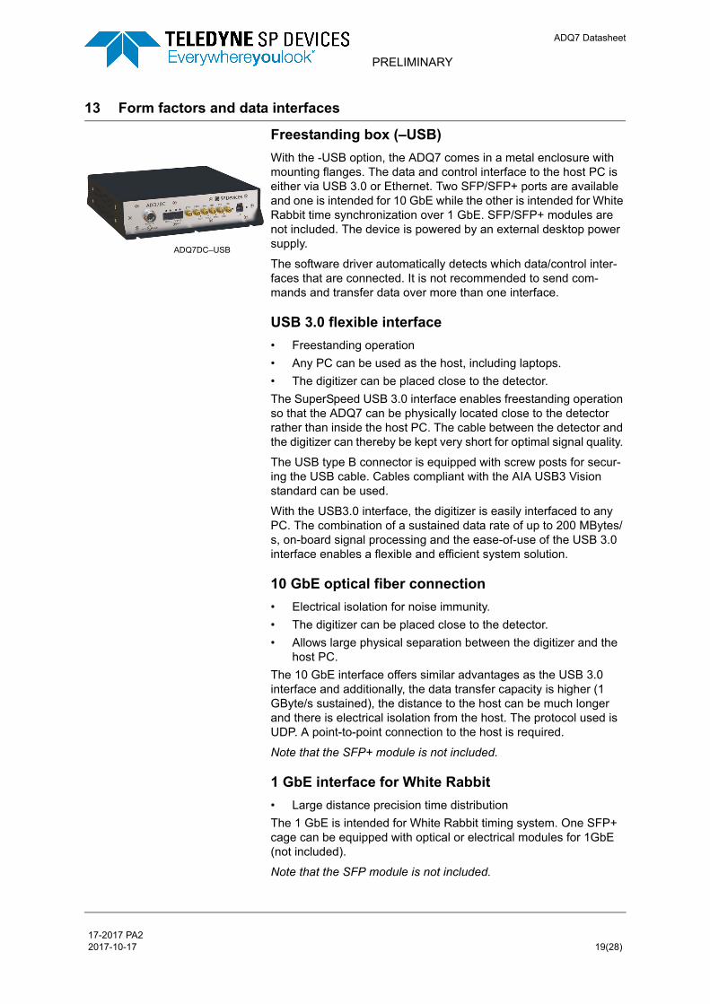
Freestanding box (–USB)
With the -USB option, the ADQ7 comes in a metal enclosure with mounting flanges. The data and control interface to the host PC is either via USB 3.0 or Ethernet. Two SFP/SFP+ ports are available and one is intended for 10 GbE while the other is intended for White Rabbit time synchronization over 1 GbE. SFP/SFP+ modules are not included. The device is powered by an external desktop power supply.
The software driver automatically detects which data/control inter-faces that are connected. It is not recommended to send com-mands and transfer data over more than one interface.
USB 3.0 flexible interface
• Freestanding operation
• Any PC can be used as the host, including laptops.
• The digitizer can be placed close to the detector.
The SuperSpeed USB 3.0 interface enables freestanding operation so that the ADQ7 can be physically located close to the detector rather than inside the host PC. The cable between the detector and the digitizer can thereby be kept very short for optimal signal quality.
The USB type B connector is equipped with screw posts for secur-ing the USB cable. Cables compliant with the AIA USB3 Vision standard can be used.
With the USB3.0 interface, the digitizer is easily interfaced to any PC. The combination of a sustained data rate of up to 200 MBytes/s, on-board signal processing and the ease-of-use of the USB 3.0 interface enables a flexible and efficient system solution.
10 GbE optical fiber connection
• Electrical isolation for noise immunity.
• The digitizer can be placed close to the detector.
• Allows large physical separation between the digitizer and the host PC.
The 10 GbE interface offers similar advantages as the USB 3.0 interface and additionally, the data transfer capacity is higher (1 GByte/s sustained), the distance to the host can be much longer and there is electrical isolation from the host. The protocol used is UDP. A point-to-point connection to the host is required.
Note that the SFP+ module is not included.
1 GbE interface for White Rabbit
• Large distance precision time distribution
The 1 GbE is intended for White Rabbit timing system. One SFP+ cage can be equipped with optical or electrical modules for 1GbE (not included).
Note that the SFP module is not included.
ADQ7DC–USB
17-2017 PA2 2017-10-17 19(28)
ADQ7 Datasheet
PRELIMINARY
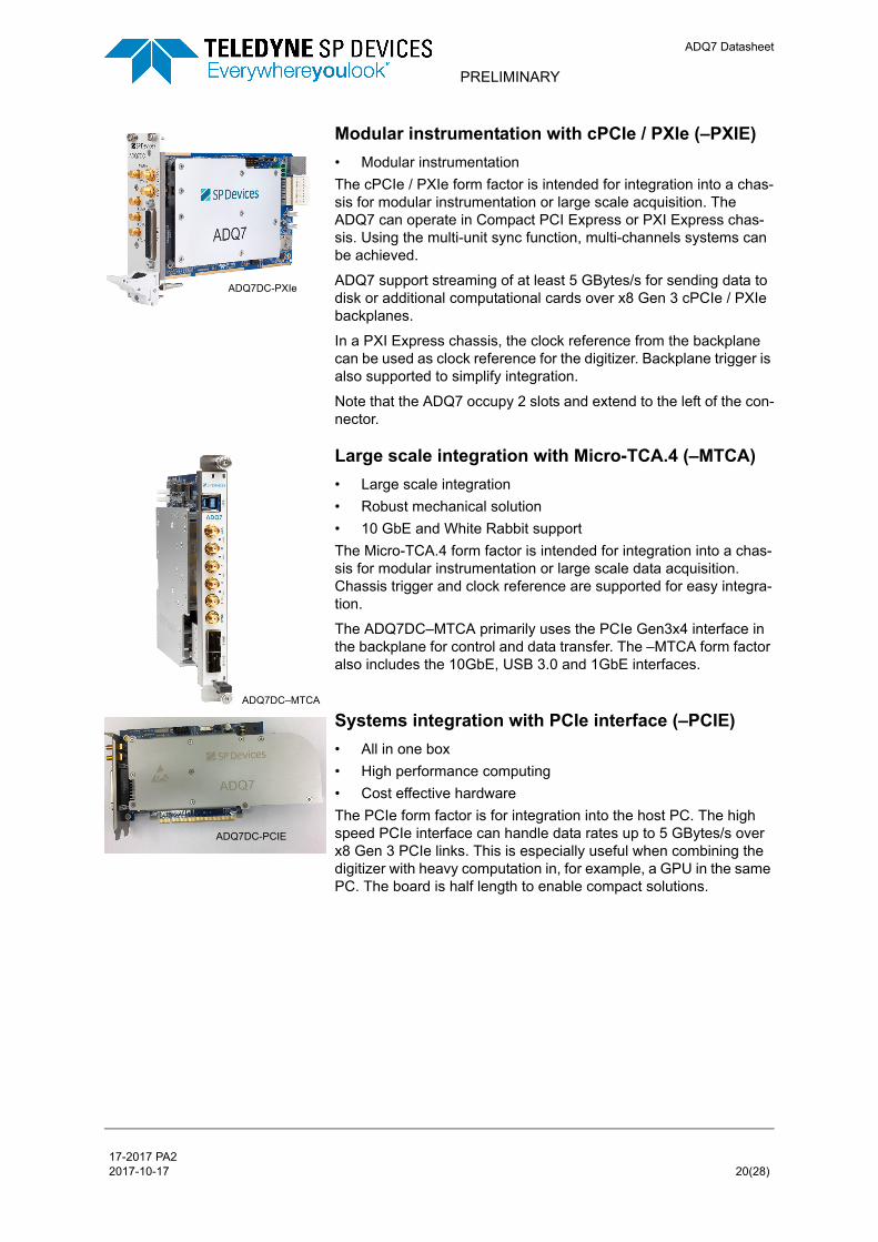
Modular instrumentation with cPCIe / PXIe (–PXIE)
• Modular instrumentation
The cPCIe / PXIe form factor is intended for integration into a chas-sis for modular instrumentation or large scale acquisition. The ADQ7 can operate in Compact PCI Express or PXI Express chas-sis. Using the multi-unit sync function, multi-channels systems can be achieved.
ADQ7 support streaming of at least 5 GBytes/s for sending data to disk or additional computational cards over x8 Gen 3 cPCIe / PXIe backplanes.
In a PXI Express chassis, the clock reference from the backplane can be used as clock reference for the digitizer. Backplane trigger is also supported to simplify integration.
Note that the ADQ7 occupy 2 slots and extend to the left of the con-nector.
Large scale integration with Micro-TCA.4 (–MTCA)
• Large scale integration
• Robust mechanical solution
• 10 GbE and White Rabbit support
The Micro-TCA.4 form factor is intended for integration into a chas-sis for modular instrumentation or large scale data acquisition. Chassis trigger and clock reference are supported for easy integra-tion.
The ADQ7DC–MTCA primarily uses the PCIe Gen3x4 interface in the backplane for control and data transfer. The –MTCA form factor also includes the 10GbE, USB 3.0 and 1GbE interfaces.
Systems integration with PCIe interface (–PCIE)
• All in one box
• High performance computing
• Cost effective hardware
The PCIe form factor is for integration into the host PC. The high speed PCIe interface can handle data rates up to 5 GBytes/s over x8 Gen 3 PCIe links. This is especially useful when combining the digitizer with heavy computation in, for example, a GPU in the same PC. The board is half length to enable compact solutions.
ADQ7DC-PXIe
ADQ7DC–MTCA
ADQ7DC-PCIE
17-2017 PA2 2017-10-17 20(28)

ADQ7 Datasheet
PRELIMINARY
14 Synchronization support
Clock reference input and output
Sharing clock reference guarantees a common time base.
When outputting the internal clock reference the ADQ7 ac as mas-ter. Use the clock reference input when the external equipment sup-ply the clock reference.
Trigger input and output
The trigger starts the operation simultaneously.
The trigger marks the start of an operation. The ADQ7 can generate a trigger to start external equipment. It can also take a trigger as input to start the acquisition.
Synchronization input and output
Extra trigger to mark beginning of a sequence.
The sync pin can be used as an input for resetting the time-stamp counter. It can also be used as an output for broadcasting an arm command to several ADQ7 units.
Time-stamp
A real-time value for each trigger.
The time-stamp is a real-time value for each trigger event. The time-stamp allows precise analysis of the timing relationship of dif-ferent acquisitions from the same or different ADQ7 units.
Sub-sample precision time-stamp
High precision external trigger.
The external trigger timing precision is four times higher than the sampling time period for precise timing analysis. The subsample precision of the time-stamp also allows for automatic analysis of trigger signal timing.
Bussed connection
Save cabling by bussed connections.
The sync, trig and clock reference can be set in high impedance mode to enable bussed connections.For best signal integrity, SMA tee adapters should be used at the high-impedance inputs to mini-mize the length of the unterminated stubs.
White Rabbit time distribution
Building a system covering several kilometers of distance.
Using a White Rabbit Ethernet-based time distribution network allows the sampling clock and time-stamp of ADQ7 to be locked to a central clock with sub-nanosecond precision over a distance of several km. See Section 12 for more details.
�� �����������
������
������
���
���
�����������������
������������������� �����������
����
����
����
���
���
��� ���������� ��
��� ���������� ������
����� ����
����������
������ �
� ����
�$%))*$
�*��$�
�%�*+�����
����� �� �
������� �� �
���������
�����������
��� ��� ��� ���
�� � �� � �� ����� ���
17-2017 PA2 2017-10-17 21(28)

ADQ7 Datasheet
PRELIMINARY
15 Built-in signal processing
Gain and offset calibration
Digital signal tuning in the FPGA.
The user can set gain and offset parameters that are applied to the digitized signal immediately after the analog-to-digital converters. This can e.g. be useful to compensate for system offsets and sim-plify later signal processing in the host computer.
Level trigger
Data driven acquisition.
The standard firmware contains a level trigger for data driven acqui-sition. The firmware option –FWPD contains more advanced pulse detection and analysis functionality. The –FWPD also contains zero-suppression to reduce the amount of data.
DBS – Digital baseline stabilizer
Enable accurate pulse detection
SP Devices’ proprietary technology for baseline stabilization, DBS, tracks and compensates for baseline variations to suppress, for example, temperature drift in the detector. This enables accurate triggering even on small pulses and eliminates interleaving pattern noise, which can be particularly important when averaging many acquisitions. The precision of DBS is as high as 22 bits.
ADX interleaving technology
Maximize spectral purity over a large bandwidth.
SP Devices’ proprietary interleaving technology ADX is available in the firmware option –FWSDR. ADX dynamically suppresses inter-leaving artifacts to produce a pure spectrum.
Waveform averaging
Data reduction in scheduled repeated measurements.
The firmware option -FWATD offers advanced averaging of wave-forms to bring out the signal from the noise when acquiring repeat-ing waveforms.
DDC for SDR
Quadrature Mixer and decimation.
The firmware option -FWSDR is a flexible software defined radio firmware that can operate in several different modes such as an IQ IF receiver or as a dual multi-channel receiver. The firmware incor-porates numerically controlled oscillators, quadrature mixers and decimation blocks to extract the channels of interest.
Custom real-time processing
Efficient real-time algorithm implementation.
The ADQ7 Development Kit opens the FPGA for custom implemen-tation of real-time algorithms. See Section 12 for more information.
���������������
���
�� �
�����
����
���
���&&����)��&��&�)�
������ �����
�����
�����
���
�������
����
�������� ���
�����
�
������
((���
���
���
�������������
������
17-2017 PA2 2017-10-17 22(28)
ADQ7 Datasheet
PRELIMINARY
16 Appendix
16.1 Connectors
All connectors have some form of locking function to prevent cables from accidentally coming loose.
16.2 LED descriptions
16.3 ADQ7–PXIE and ADQ7–PCIE GPIO
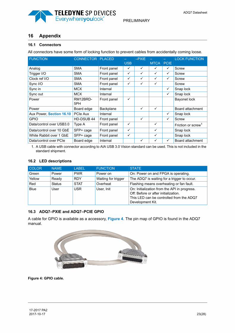
A cable for GPIO is available as a accessory, Figure 4. The pin map of GPIO is found in the ADQ7 manual.
FUNCTION CONNECTOR PLACED –USB
–PXIE –MTCA
–PCIE
LOCK FUNCTION
Analog SMA Front panel Screw
Trigger I/O SMA Front panel Screw
Clock ref I/O SMA Front panel Screw
Sync I/O SMA Front panel Screw
Sync in MCX Internal Snap lock
Sync out MCX Internal Snap lock
Power RM12BRD-5PH
Front panel Bayonet lock
Power Board edge Backplane Board attachment
Aux Power, Section 16.10 PCIe Aux Internal Snap lock
GPIO HD-DSUB 44 Front panel Screw
Data/control over USB3.0 Type A Front panel Friction or screw1
1. A USB cable with connector according to AIA USB 3.0 Vision standard can be used. This is not included in the standard shipment.
Data/control over 10 GbE SFP+ cage Front panel Snap lock
White Rabbit over 1 GbE SFP+ cage Front panel Snap lock
Data/control over PCIe Board edge Internal Board attachment
COLOR NAME LABEL FUNCTION STATE
Green Power PWR Power on On: Power on and FPGA is operating.
Yellow Ready RDY Waiting for trigger The ADQ7 is waiting for a trigger to occur.
Red Status STAT Overheat Flashing means overheating or fan fault.
Blue User USR User, Init On: Initialization from the API in progress.Off: Before or after initialization.This LED can be controlled from the ADQ7 Development Kit.
Figure 4: GPIO cable.
17-2017 PA2 2017-10-17 23(28)
ADQ7 Datasheet
PRELIMINARY
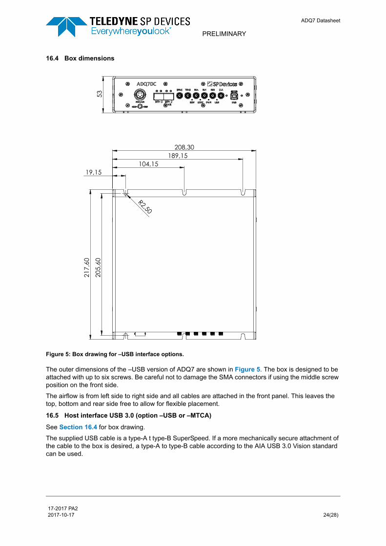
16.4 Box dimensions
The outer dimensions of the –USB version of ADQ7 are shown in Figure 5. The box is designed to be attached with up to six screws. Be careful not to damage the SMA connectors if using the middle screw position on the front side.
The airflow is from left side to right side and all cables are attached in the front panel. This leaves the top, bottom and rear side free to allow for flexible placement.
16.5 Host interface USB 3.0 (option –USB or –MTCA)
See Section 16.4 for box drawing.
The supplied USB cable is a type-A t type-B SuperSpeed. If a more mechanically secure attachment of the cable to the box is desired, a type-A to type-B cable according to the AIA USB 3.0 Vision standard can be used.
Figure 5: Box drawing for –USB interface options.
��������
�������������
����
� ��
������
���
� ��
������
���
������*�����
!*�����������������*���*������!��������*����
17-2017 PA2 2017-10-17 24(28)
ADQ7 Datasheet
PRELIMINARY
16.6 Host interface 10GbE (option –USB or –MTCA)
The ADQ7–USB is equipped with two SFP+ cages that accept SFP / SFP+ modules. The interface is tested with these modules:
• Avago AFBR-709SMZ
• Intel SFP+ E10GSFPSR
Correct operation can only be guaranteed with these modules. The modules are not included.
The cage marked SFP+1 is the primary cage for 10GbE connection.
The cage marked SFP+2 WR is intended for White Rabbit 1GbE timing solution.
16.7 Host interface 1GbE (option –USB or –MTCA)
The SFP/SFP+ cage marked "SFP+2 WR" on ADQ7DC-USB and ADQ7DC-MTCA accepts an SFP module for 1 GbE. This interface is primarily intended for interfacing to a White Rabbit time distribution network.
Note that White Rabbit support is available when using any of the data interfaces Micro-TCA.4, USB 3.0 and 10GbE
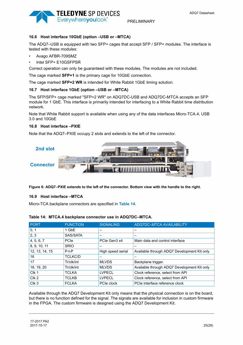
16.8 Host interface –PXIE
Note that the ADQ7–PXIE occupy 2 slots and extends to the left of the connector.
16.9 Host interface –MTCA
Micro-TCA backplane connectors are specified in Table 14.
Available through the ADQ7 Development Kit only means that the physical connection is on the board, but there is no function defined for the signal. The signals are available for inclusion in custom firmware in the FPGA. The custom firmware is designed using the ADQ7 Development Kit.
Figure 6: ADQ7–PXIE extends to the left of the connector. Bottom view with the handle to the right.
Table 14: MTCA.4 backplane connector use in ADQ7DC–MTCA.
PORT FUNCTION SIGNALING ADQ7DC–MTCA AVAILABILITY
0, 1 1 GbE – –
2, 3 SAS/SATA – –
4, 5, 6, 7 PCIe PCIe Gen3 x4 Main data and control interface
8, 9, 10, 11 SRIO – –
12, 13, 14, 15 P-t-P High speed serial Available through ADQ7 Development Kit only
16 TCLKC/D – –
17 Tr/clk/int MLVDS Backplane trigger.
18, 19, 20 Tr/clk/int MLVDS Available through ADQ7 Development Kit only
Clk 1 TCLKA LVPECL Clock reference, select from API
Clk 2 TCLKB LVPECL Clock reference, select from API
Clk 3 FCLKA PCIe clock PCIe interface reference clock
Connector
2nd slot
17-2017 PA2 2017-10-17 25(28)
ADQ7 Datasheet
PRELIMINARY
16.10 Host interface –PCIE
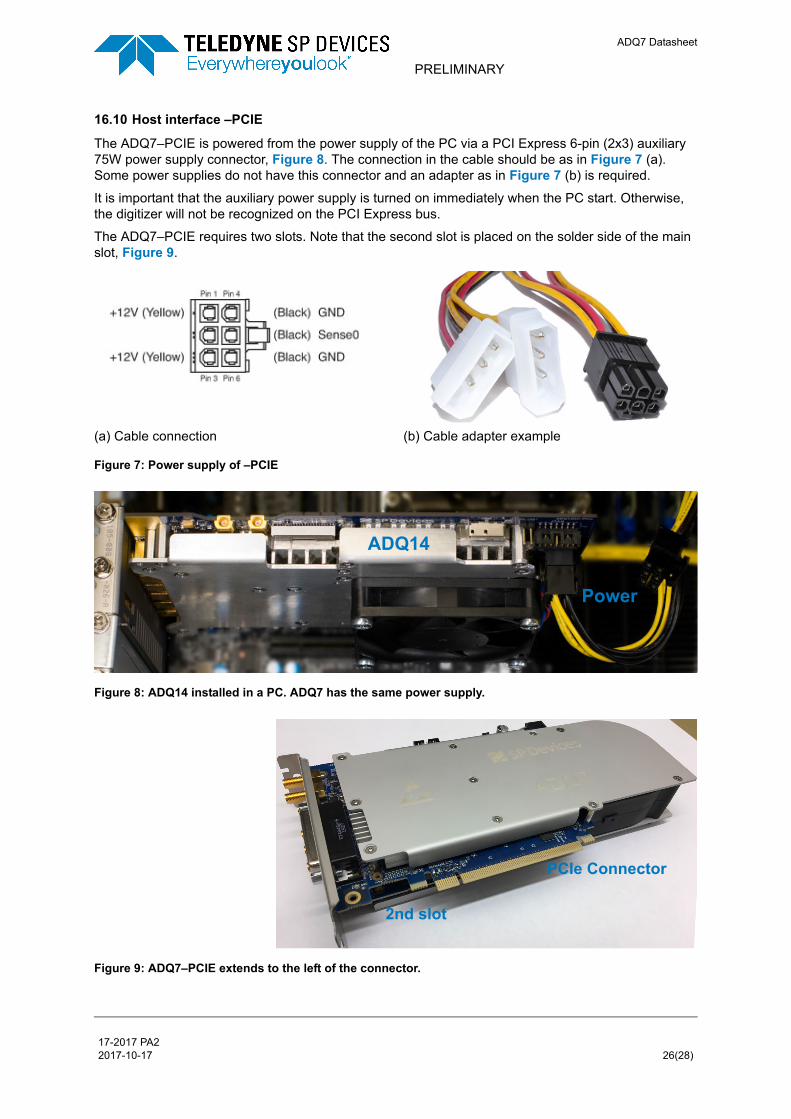
The ADQ7–PCIE is powered from the power supply of the PC via a PCI Express 6-pin (2x3) auxiliary 75W power supply connector, Figure 8. The connection in the cable should be as in Figure 7 (a). Some power supplies do not have this connector and an adapter as in Figure 7 (b) is required.
It is important that the auxiliary power supply is turned on immediately when the PC start. Otherwise, the digitizer will not be recognized on the PCI Express bus.
The ADQ7–PCIE requires two slots. Note that the second slot is placed on the solder side of the main slot, Figure 9.
(a) Cable connection (b) Cable adapter example
Figure 7: Power supply of –PCIE
Figure 8: ADQ14 installed in a PC. ADQ7 has the same power supply.
Figure 9: ADQ7–PCIE extends to the left of the connector.
ADQ14
Power
PCIe Connector
2nd slot
17-2017 PA2 2017-10-17 26(28)
ADQ7 Datasheet
PRELIMINARY
Ordering information
References
16-1787 ADQ7 presentation
16-1794 ADQ7-FWATD datasheet
16-1793 ADQ7-FWPD datasheet
16-1795 ADQ7-FWSDR datasheet
16-1796 ADQ7 manual
ORDERING INFORMATION
ADQ7 DC-coupled ADQ7DC
AVAILABLE OPTIONS
Host PC interface –USB, –PCIE, –MTCA, –PXIE,
Firmware options –FWDAQ, –FWATD, –FWPD, –FWSDR
RELATED PRODUCTS
ADQ7 Development Kit for FWDAQ –DEV7DAQ
ADQ7 Development Kit for FWPD –DEV7PD
AIA USB3 Vision cable with screw lock 108-002-006
GPIO cable 1m, 2 connectors 108-004-004
17-2017 PA2 2017-10-17 27(28)

SWEDEN | Signal Processing Devices Sweden AB | Teknikringen 6, SE-583 30 Linköping | Phone: +46 (0) 13 4650600 | Fax: +46 (0) 13 991 3044
SWITZERLAND | Signal Processing Devices | 275, Route de Saint-Julien, CH-1258 Perly, Geneva | Phone: +41 78 845 5657
US | Signal Processing Devices Inc. | 2603 Camino Ramon, Suite 200, San Ramon CA 94583 | Phone: +1 415 533 1341
www.spdevices.com
ADQ7 Datasheet17-2017-PA2 2017-10-17
PRELIMINARY 28(28)
Important Information
Teledyne Signal Processing Devices Sweden AB (Teledyne SP Devices) reserve the right to make cor-rections, modifications, enhancements, improvements, and other changes to its products and services at any time and to discontinue any product or service without notice. Customers should obtain the latest relevant information before placing orders and should verify that such information is current and com-plete. All products are sold subject to Teledyne SP Devices’ general terms and conditions supplied at the time of order acknowledgment.
Teledyne SP Devices warrants that each product will be free of defects in materials and workmanship, and conform to specifications set forth in published data sheets, for a period of one (1) year. The war-ranty commences on the date the product is shipped by Teledyne SP Devices. Teledyne SP Devices’ sole liability and responsibility under this warranty is to repair or replace any product which is returned to it by Buyer and which Teledyne SP Devices determines does not conform to the warranty. Product returned to Teledyne SP Devices for warranty service will be shipped to Teledyne SP Devices at Buyer’s expense and will be returned to Buyer at Teledyne SP Devices’ expense. Teledyne SP Devices will have no obligation under this warranty for any products which (i) has been improperly installed; (ii) has been used other than as recommended in Teledyne SP Devices’ installation or operation instruc-tions or specifications; or (iii) has been repaired, altered or modified by entities other than Teledyne SP Devices. The warranty of replacement products shall terminate with the warranty of the product. Buyer shall not return any products for any reason without the prior written authorization of Teledyne SP Devices.
In no event shall Teledyne SP Devices be liable for any damages arising out of or related to this docu-ment or the information contained in it.
TELEDYNE SP DEVICES’ EXPRESS WARRANTY TO BUYER CONSTITUTES TELEDYNE SP DEVICES’ SOLE LIABILITY AND THE BUYER’S SOLE REMEDY WITH RESPECT TO THE PROD-UCTS AND IS IN LIEU OF ALL OTHER WARRANTIES, LIABILITIES AND REMEDIES. EXCEPT AS THUS PROVIDED, TELEDYNE SP DEVICES DISCLAIMS ALL WARRANTIES, EXPRESS OR IMPLIED, INCLUDING ANY WARRANTY OF MERCHANTABILITY, FITNESS FOR A PARTICULAR PURPOSE OR NON-INFRINGEMENT.
TELEDYNE SP DEVICES DOES NOT INDEMNIFY, NOR HOLD THE BUYER HARMLESS, AGAINST ANY LIABILITIES, LOSSES, DAMAGES AND EXPENSES (INCLUDING ATTORNEY’S FEES) RELAT-ING TO ANY CLAIMS WHATSOEVER. IN NO EVENT SHALL TELEDYNE SP DEVICES BE LIABLE FOR SPECIAL, INCIDENTAL OR CONSEQUENTIAL DAMAGES, INCLUDING LOST PROFIT, LOST DATA AND THE LIKE, DUE TO ANY CAUSE WHATSOEVER. NO SUIT OR ACTION SHALL BE BROUGHT AGAINST TELEDYNE SP DEVICES MORE THAN ONE YEAR AFTER THE RELATED CAUSE OF ACTION HAS ACCRUED. IN NO EVENT SHALL THE ACCRUED TOTAL LIABILITY OF TELEDYNE SP DEVICES FROM ANY LAWSUIT, CLAIM, WARRANTY OR INDEMNITY EXCEED THE AGGREGATE SUM PAID TO SP BY BUYER UNDER THE ORDER THAT GIVES RISE TO SUCH LAWSUIT, CLAIM, WARRANTY OR INDEMNITY.
Worldwide Sales and Technical Support
www.spdevices.com
Teledyne SP Devices Corporate Headquarters
Teknikringen 6SE-583 30 LinköpingSweden
Phone: +46 (0)13 465 0600Fax: +46 (0)13 991 3044Email: [email protected]
Copyright © 2017 Teledyne Signal Processing Devices Sweden AB. All rights reserved, including those to repro-duce this publication or parts thereof in any form without permission in writing from Teledyne SP Devices.