semiconductor ic test and design-for-test...
TRANSCRIPT

Semiconductor IC Test and Design-for-Test Fundamentals
By Al Crouch, Chief Scientist, Inovys Corporation
The Semiconductor Industry seeks to reduce the cost of manufacturing its product by
continuously reducing the per-part recurring costs in the following manner:
- Reduction of silicon cost by increasing volume and yield, and by die size reduction (process shrinks or more efficient layout)
- Reduction of packaging cost by increasing volume, shifting to lower cost packages if possible (e.g., from ceramic to plastic), or reduction in package pin count
- Reduction in cost of test by:
- reducing the vector data size
- reducing the tester sequencing complexity
- reducing the cost of the tester
- reducing test time
- simplifying the test program
Design for test contributes to all three fundamental strategies.
• Test and Design-for-Test Fundamentals Page 2 of 22
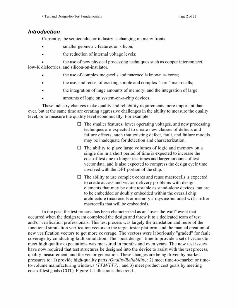
Introduction Currently, the semiconductor industry is changing on many fronts:
• smaller geometric features on silicon;
• the reduction of internal voltage levels;
• the use of new physical processing techniques such as copper interconnect, low-K dielectrics, and silicon-on-insulator,
• the use of complex megacells and macrocells known as cores;
• the use, and reuse, of existing simple and complex "hard" macrocells;
• the integration of huge amounts of memory; and the integration of large
• amounts of logic on system-on-a-chip devices.
These industry changes make quality and reliability requirements more important than ever, but at the same time are creating aggressive challenges in the ability to measure the quality level, or to measure the quality level economically. For example:
The smaller features, lower operating voltages, and new processing techniques are expected to create new classes of defects and failure effects, such that existing defect, fault, and failure models may be inadequate for detection and characterization.
The ability to place large volumes of logic and memory on a single die in a short period of time is expected to increase the cost-of-test due to longer test times and larger amounts of test vector data, and is also expected to compress the design cycle time involved with the DFT portion of the chip.
The ability to use complex cores and reuse macrocells is expected to create access and vector delivery problems with design elements that may be quite testable as stand-alone devices, but are to be embedded or doubly embedded within the overall chip architecture (macrocells or memory arrays are included with other macrocells that will be embedded).
In the past, the test process has been characterized as an "over-the-wall" event that occurred when the design team completed the design and threw it to a dedicated team of test and/or verification professionals. This test process was largely the translation and reuse of the functional simulation verification vectors to the target tester platform. and the manual creation of new verification vectors to get more coverage. The vectors were laboriously "graded" for fault coverage by conducting fault simulation. The "post design" time to provide a set of vectors to meet high quality expectations was measured in months and even years. The new test issues have now required that test structures be designed into the device to assist with the test process, quality measurement, and the vector generation. These changes are being driven by market pressures to: 1) provide high-quality parts (Quality/Reliability); 2) meet time-to-market or time-to-volume manufacturing windows (TTM/TTV); and 3) meet product cost goals by meeting cost-of-test goals (COT). Figure 1-1 illustrates this trend.
• Test and Design-for-Test Fundamentals Page 3 of 22
Concurrent Test Engineering The rapid pace of process geometry reduction in recent times has led to a strange cost/
pricing effect. Whereas in the past, the overall cost of the semiconductor product has been able to be cost managed to a lower level over time, lags in supporting technology have finally led to "smaller is more expensive." There is currently a reasonable die size limit to the ability to con-nect bonding wires from the package to the silicon. This has led to a somewhat "limited" die size for certain pin count packages. If a process geometry shrink is applied to an existing device, then the logic may not fill up the space within the pad ring. To eliminate this "white space; the chip design organizations are adding more functionality or memory arrays. These significantly increase test time and test vector data. If the memory supported on the chip, or the additional memory added, is a non-volatile memory (Flash, EEPROM), then test time is also significantly increased, since these types of memories require long test times naturally.
Another test cost impact has been the adoption of the "reuse" hard core macrocell (for example, an entire microprocessor as a megacell). For intellectual property (IP) security reasons, hard core macrocells from core providers are delivered complete with existing test vectors (hav-ing the ability to generate vectors against a structural description of a provider's core may give away all the proprietary internal features for the core). Semiconductor devices made with many hard cores require building test programs out of many vector sets delivered by the core providers. The vector sets may not be very efficient, or may not be able to be applied simultaneously to other vector sets. This fact leads to a high cost-of-test in having a complicated "patchwork" test program.
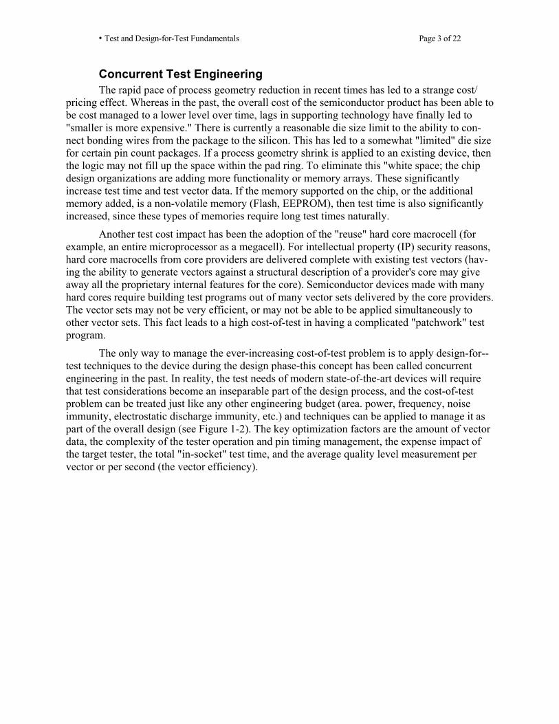
The only way to manage the ever-increasing cost-of-test problem is to apply design-for--test techniques to the device during the design phase-this concept has been called concurrent engineering in the past. In reality, the test needs of modern state-of-the-art devices will require that test considerations become an inseparable part of the design process, and the cost-of-test problem can be treated just like any other engineering budget (area. power, frequency, noise immunity, electrostatic discharge immunity, etc.) and techniques can be applied to manage it as part of the overall design (see Figure 1-2). The key optimization factors are the amount of vector data, the complexity of the tester operation and pin timing management, the expense impact of the target tester, the total "in-socket" test time, and the average quality level measurement per vector or per second (the vector efficiency).
• Test and Design-for-Test Fundamentals Page 4 of 22
Figure 1-2 Design process

• Test and Design-for-Test Fundamentals Page 5 of 22
Figure 1-3 Why Test?

• Test and Design-for-Test Fundamentals Page 6 of 22
The Reasons for Testing
Why Test? Why Add Test Logic? Basically, there are two real reasons to conduct testing. As shown in Figure 1-3, it is con-
tractually required by a specific customer (or by generic customers by way of an implied or actual warranty); or it is required by a competitive environment where the quality level and device reliability are among the items voted on by customer dollars.
Test logic may be added for several reasons. Some key reasons cited quite often are "to increase the test coverage" and "to reduce the time it takes to qualify the part" (deliver vectors that meet a certain test coverage). Many organizations are now beginning to understand that "reducing the cost-of-test" by supporting test features during the design phase is manageable, achievable, and can be treated as an engineering problem with a set of targetable goals. The act of adding logic or features to enhance the testability of a design is generally referred to as Design-for-Test (DFT). More specifically, DFT can be defined as adding logic or features to enhance the ability to achieve a high quality metric, to ease the ability to generate vectors, to reduce the time involved with vector generation, or to reduce the cost involved with the application of vectors.
Pro and Con Perceptions of DFT Whenever testing and design-for-test is brought up as a subject, people and organizations
have differing opinions and perceptions. For design engineering organizations and individuals, the perception of DFT is generally negative:
• it adds work and complication to the design methodology flow • it negatively impacts chip design budgets such as
o power area timing o package pin requirements
• it adds tasks and risk to the design schedule
However, for test professionals, the perceptions of DFT are usually positive and include such items as:
having the ability to measure the quality level deterministically making it easier to generate the necessary vectors; making it possible to support all test environments easily wafer probe manufacturing test burn-in life-cycle board-level integration engineering debug customer return debug
process characterization yield enhancement and failure analysis allowing the cost-of-test to be reduced in all environments reduces tester complexity (and cost) reduces tester time (and cost) reduces tester requirements (pins, memory depth, pin timing)
• Test and Design-for-Test Fundamentals Page 7 of 22
However, much of this perception is true only if the additional logic added for test is designed to meet these goals. In many organizations, some test logic is still added in an ad hoc manner to meet specific goals, which has limited payback in the larger scheme of things.
Figure 1-4 Definition of Testing
• Test and Design-for-Test Fundamentals Page 8 of 22
The Definition of Testing
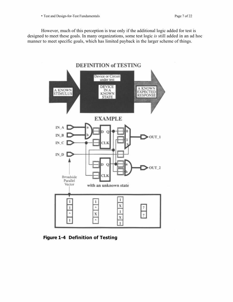
What Is Testing? The definition of testing is a rather simple concept and it applies equally to chips, boards,
and systems: testing is possible when a known input stimulus is applied to a unit in a known state, and a predictable or known response can be evaluated. In general, as Figure 1-4 shows, the known response from a circuit is compared to an "ideal" or "golden" expected response.
A Known Input Stimulus Testing can be accomplished on any level of circuitry from transistors to gates to
macrocells to cores to chips to boards to systems. Any kind of testing requires putting a known input stimulus into the unit-to-be-tested's input pins. This input stimulus can be applied in a simulator, on a tester, or from other logic within the system. For digital systems, this stimulus is in the form of logic 1's and 0's known as vectors. Having the ability to apply the stimulus to the unit under test is generally referred to as controllability.
A Known State For testing to be valid, the unit-to-be-tested must be in a known state. It doesn't matter
what stimulus is applied if the internal state of the circuitry is not known explicitly. The unit-to--be-tested must act as a simple linear operator-in other words, if "A" is applied. "B" happens (every time). This result is not true if randomness exists. The repeatability of operations is known as determinism, and the repeatable response of the unit-under-test is generally termed as being deterministic.
Placing a circuit into a known state can be done by applying a set of initialization values that will result in a known state unconditionally, or by applying some form of hardware set/reset that will leave the logic in a known state.
A Known Expected Response The third requirement for valid testing is being able to evaluate a known expected
response. For digital systems, this determination requires having a pre-conceived notion of the system function (e.g., a specification for the action, the truth table for a logic gate, etc.) or by simulation of vectors to get a set of expected response vectors against which to compare the circuit response. The ability to evaluate the output response of the unit-under-test is generally referred to as observability.
The key here is access to the output values and the ability to compare the circuit response to a known expected value. The same problems that affect applying a known input stimulus are valid here. The output response must be detected directly or translated through "tested-known--good" logic, or through a special logic access structure, to a point where it can be detected (observed), and then it must be compared to a pre-determined known value.
Stimulus The term stimulus or input stimulus, when referring to electronics testing, generally
refers to one of two items: logical 1's and 0's. which translate to voltage levels for digital testing (for example, TTL levels refer to voltages of 0V minimum and 5V maximum to
• Test and Design-for-Test Fundamentals Page 9 of 22
represent a logic 0 and logic 1, respectively); and analog waveforms that may be represented as functions of voltage or current. When applied as a grouping of some sort (for example, the set of l's and 0's applied to multiple chip pins at one clock cycle edge), the stimulus is generally referred to as vectors. Usually, the term patterns represents collections of vectors bundled together into a single file.
Response The response or output response of a device during digital testing may actually
involve more that just a logic 1 or logic 0. In general, the concepts of unknown (indeterminate) and high impedance must also exist. These values are generally referred to as logic X's and Z's, respectively.
The majority of IC testing involves "voltage level" evaluation, but current measurement and time-based waveform analysis are also common descriptions of output response.
Transistor and Gate Representation of Defects, Faults, and Failures

• Test and Design-for-Test Fundamentals Page 10 of 22
Test Measurement Criteria
What Is Measured? When a known stimulus has been applied to an initialized circuit and the response
has been evaluated and is found to not match the expected response, then a failure has occurred. However, in the language of test, the terms defects and faults are used in addition to the term failure. Each of these terms has a different meaning in the test process, shown in Figure 1-5.
Defects Defects are the physical problems that occur in silicon. Different processes and process
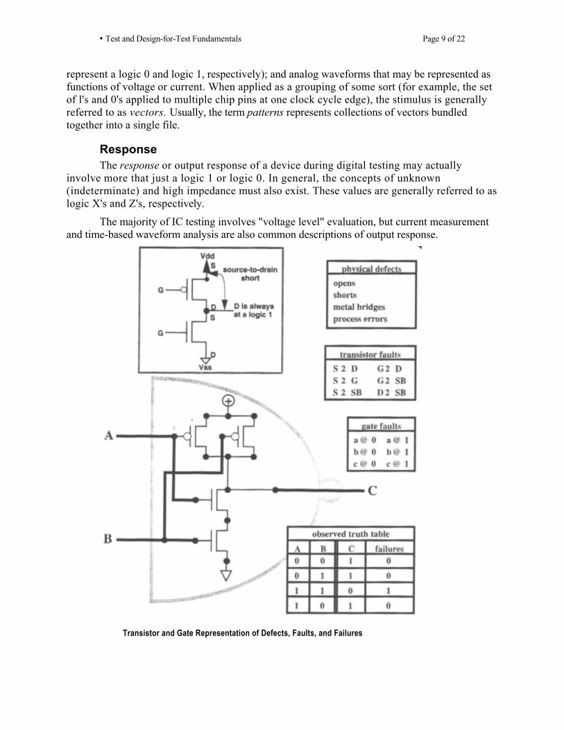
geometries (feature sizes) have different groupings of problems that manifest themselves as defects. Some common silicon CMOS (complementary metal oxide semiconductor) defects are: gate-oxide shorts, insufficient doping, process or mask errors, metal trace opens, metal trace bridges (resistive and 0 ohm), open and plugged vias (anomalies in the vertical interconnections between metal layers), and shorts to Power (Vdd) or Ground (Vss).
Faults A fault can be viewed as the failure-mode manifestation of the defect. The fault is a
model of the failure mode of the defect that relates the defect to circuit behavior. For example, a gate-oxide short effectively shorts the source of a transistor to that transistor's drain. This creates the transistor-level fault of a shorted "source-to-drain" (referred to in Figure 1-5 as S2D). These faults may be modeled by sticking the output of the transistor to a fixed logic value (logic 1 or 0). Other transistor fault models can represent the shorts or opens in the "gate-to-drain" (G2D) or in the "source-to-substrate" (S2SW portions of the transistor. The behavior resulting from these models may be high current, a high impedance state, or intermittent behavior.
In the case of the gate-level description, the model most used for quality measurement is the single-stuck-at fault.
Another example of a defect mapping to a fault is the small metal open on a connection trace. In this case, the logic value can still propagate, but by a tunneling current across the open. The propagation of the logic value is slowed as if it were passed through a series resistance. The fault model at the circuit level is to represent the defect as a unit of signal delay along the length of the signal trace. This fault model is generally known as a delay fault.
Failures Many defects may exist, and these defects may all map to fault models, but a defect, or a
transistor level fault, or a gate-level fault may not represent a failure. The term failure has two requirements that must be met: 1) that the fault model be exercisable and observable; and 2) that failure measurement criteria be established.
However, if the circuit is constructed with redundancy so that the NAND-gate cannot be exercised to the proper sure or so that the NAND-gate response cannot be observed, then the fault exists, but not the failure. The fault may be classified as undetected, blocked, tied,

• Test and Design-for-Test Fundamentals Page 11 of 22
redundant, or untestable, and may or may not be counted in the fault detection metric. Some examples of faults that are not failures would be:
− small delay faults on paths with large timing margins
− stuck-at faults on redundant or reconvergent fanout logic
− current leakage less than an established level
For these examples, the chip would have a defect content, but not a fail indication. The manifestation of the defects may be as a reliability problem, which should be screened out as infant mortality during an early exercise process such as burn-in (accelerated life-cycle testing by continuous operation of the device in an environmental chamber or oven).
Fault Metric Mathematics A common metric used as quality assessment on digital circuits is fault coverage. Fault
coverage is related to another term known as vector grading (also more commonly referred to as fault grading). The measurement of fault coverage is done with reference to a set of vectors. The vectors are said to exercise and detect some measured number of faults out of all possible faults in the design.
The general mathematical equation for fault coverage is:
(Total Detected Faults) / (Total Fault Population)
For example, (9821 detected faults)/( 10,000 total faults) = 98.21% fault coverage. There is a warning about fault coverage, however. Different tools may report different
fault coverage numbers. Sometimes the absolute total number of faults in the design is not used as the denominator of the measurement process - in these cases, the denominator may be reduced by the number of "untestable faults" due to the circuit configuration (redundant, tied, blocked, constrained, etc.), since this content is constant and based on the design. The discrepancy in fault coverage also occurs when different tools identify faults differently so the total fault population changes. For example, some tools may classify only stuck-at 1's and 0's on gate inputs and outputs as faults, whereas other tools may classify stuck-at 1 's and 0's on gate inputs, gate outputs, and the interconnecting wire nets as faults.

• Test and Design-for-Test Fundamentals Page 12 of 22
Figure 1-6 Fault Modeling
Fault Modeling
Physical Defects Physical defects are what really happens to the part in the physics realm. At the chip
level, these fall into many categories: interconnect defects, packaging defects, process problems, and so on. These defects have their source in such things as local contamination, lattice shifting, incorrect masks, process errors, insufficient doping, silicon die stress, and interconnect
• Test and Design-for-Test Fundamentals Page 13 of 22
errors or dicing stress. The task of a failure analysis engineer is to isolate manufacturing defects and determine their source so that yield may be maintained at an acceptable level.
Fault Modeling Fault modeling is the translation of physical defects to a mathematical construct that can
be operated upon algorithmically and understood by a software simulator for the purposes of providing a metric for quality measurement. The most common fault models supported in mod-ern VLSI and core-based digital design are the single-stuck-at DC model, the transition and path delay AC models, and current measurement models.
The Single-Stuck-At Fault Model Currently, a popular model for digital circuitry is the single-stuck-at fault. This is a
DC (static) approximation whereby all failures are represented as an individual gate-level pin port or wire net connection that acts as if it were shorted to Vdd or Vss. However, a limiting assumption is applied to the single-stuck-at fault model known as the "single-fault assumption." This assumption requires that only one fault exists at a time during any analysis, assessment, or diagnostic. The assumption is applied to reduce the complexity of the assessment (the "what if' of extrapolating multiple faults in designs with thousands of faults can become overly compute intensive to the point of impossibility with current computer technology). This model is applied regardless of frequency or time domain considerations.
The key to the gate-level stuck-at fault model is that a fault will cause a boolean gate error which, if observed, is classified as a failure. For example, for the NAND-gate in Figure 1-6, if either input A or B is stuck at logic 0 (AB@0), then the output C will always produce a logic 1 output; if input A is stuck at a logic 1 (A@ 1), then the output C will produce an incorrect output-a logic 0 instead of 1 when the A=O, B=1 input combination is applied; if the input B is stuck at a logic 1 (B @1), then the output C will produce an incorrect output-a logic 0 instead of a 1 when the A=1, B-0 input combination is applied; and finally, if the output C is stuck at logic 0 or logic 1, then the output of the NAND-gate will always be a logic 0 or logic 1, respec-tively, regardless of the applied input to the gate.
The Delay Fault Models There are two generally supported fault models for AC effects (that is, fault models that
include the concept of timing)-the transition delay and path delay fault models.
The Transition Delay Fault Model: The basic timing fault model is the transition delay model, which can be viewed as a modified version of the single-stuck-at DC model, but with an additional restriction applied to allow it to be used to assess the time domain. The extra step is to force the gate-output to the expected fail value at some time period prior to the observation event, and to then apply a transition and to conduct the observed or sample event at a defined period of time. The requirement of being observed at the fail value at an initial time and then being observed at the pass value at a second time maps a time assessment onto the simple DC stuck-at model. Instead of viewing any node, net, or gate input as a stuck-at logic 1 or 0, the transition delay fault model applies the slow-to-rise (the logic 0 to logic 1 transition) or the slow-to-fall (the logic 1 to logic 0 transition).
• Test and Design-for-Test Fundamentals Page 14 of 22
The application of the fault model to gate pin ports or wire net connections is identical to the stuck-at DC gate-level model, except that the stuck-at-0 and stuck-at-1 values are now termed zero-to-one and one-to-zero transitions (for example. the gate output C zero-to-one transition---C0-1 in the transition delay table in Figure 1-6). The transition delay fault model is also known as the gate delay fault model, since the observation of a fault can be attributed to a slow gate input or slow gate output (the delay can be related directly to a gate in the modeling sense).
The Path Delay Fault Model: The other AC fault model in common use is the path delay model. This model can be viewed as the sum (or stack up) of combinational gate transition delays along an identified circuit path. The overall model is similar to the transition delay model, but instead of a single gate pin port or wire net connection being targeted, an entire path made of multiple gate pin ports and wire net connections is the target of the fault model.
The restriction of having a fail value being observed at the output of the path at some initial time, and then having the pass value being observed at the path output at a defined later time, is still required. The path transitions are generally referred to as a concatenation of nets from the input transition point to the output observe point. For example, the path A-to-S slow-to-rise (A2SR in the path delay table in Figure 1-6) may be formally described as pin and net elements. "A-a-r-s-S Rising" (similarly. A2SF means path A-to-S slow-to-fall).
The Current-Based Fault Models Another popular set of fault models that has gained acceptance is the current-based fault
models. Some defects have been found to map to fault effects that are not caught by either the stuck-at or the delay fault models. These defects may cause high current leakage (as may the defects that are represented by the stuck-at and the delay fault model). Some organizations argue that a defect that does not cause a boolean error is not a fault or a failure condition, but is more of an indicator of a reliability problem (a condition that does not fail now, but may indicate an early failure due to a mechanism such as metal migration or an active short that will eventually create an open). The classification of a high current leakage condition as a failure condition is subjective to each organization's quality requirements, but in some cases with critical applications (such as pacemakers), any out of tolerance behavior must be classified as a failure.
In CMOS logic, quiescent current measurement is effective because non-switching gates can be modeled as only using quiescent or diode reverse current---the leakage current used by a static non-switching device should be very low (the sum of the reverse currents for the number of transistors on the device), any active bridging, shorts, and some open defects should result in a current measurement that is an order-of-magnitude greater than the “quiescent current rating”.
Quiet Vector Selection: However, an extra restriction is applied to fault models used for the current measurement technique. This requirement is that the design must be in a static or quiet state when the observation event occurs. This means that the design must not have any active current sources and sinks (such as pullup and pulldown logic) that can compromise (overwhelm) the detection of the fault. Since the current measurement is based on the "quiescent" current draw, which can be a very low limit such as 10 microAmps, then any dynamic or active logic can easily overwhelm this limit by drawing milliAmps of current.

• Test and Design-for-Test Fundamentals Page 15 of 22
Figure 1-7 Types of Testing
Types of Testing
Functional Testing A functional (or behavioral) test is used to verify that the model or logic behaves as it
was intended (specification behavior). This may also be called a "design verification test." If the function represents an adder, then tests will be written to see whether the logic commits the necessary add functions and nothing more (see Figure 1-7). For example, if 3+5 and 4+4 are the only values specified or critical to the adder, then these are the values applied to test the adder's functionality-if all values are important, then all combinations will be applied. Functional test-ing is measured by the logic committing the correct action (known expected response) to the
• Test and Design-for-Test Fundamentals Page 16 of 22
(known) applied stimulus-100% functional correctness is the standard expectation and this should be verified at the behavioral (HDL/RTL) level, or the gate-level of the design with a simulation process.
Functional testing may also include timing or power consumption as part of the functional standard. In the case of timing, a second dimension is added to the behavior of the circuit: 1) that it conduct the correct behavior; and 2) that it conduct this behavior to a timing standard. For example, if a general purpose adder is placed within a chip design and it must be able to add any two hexadecimal numbers within one clock cycle, then the goal is to provide an additional set of tests that verifies that the slowest operation conducted by the adder is still faster than the target cycle time of the device. In the case of power consumption, some defined operations must occur and the device can consume no more power than the specified power budget.
Structural Testing A structural test is used to verify the topology of the manufactured chip (see Figure 1-
7). Another way of saying this is, "Given a good circuit before the manufacturing process, structural testing can be used to verify that all connections are intact, and that all gate-level truth tables are correct after the manufacturing process." This type of testing can be done with reliance on the static stuck-at fault model. This is an assumption that the physical defect being searched for will represent itself as a net or gate connection that acts as if it is always a 1 (short to Vdd) or always a 0 (short to Vss). Tests are developed by applying values to the inputs that toggle the suspected defective node to its opposite value (forcing a 1 on a stuck-at 0 node) and then applying values at the inputs that would allow the good value to propagate to a detect point. If the value at the detect point differs from the expected value for a good circuit, then a fault has been detected. Structural testing is measured by fault coverage (how many faults were detected compared to the total number of possible faults)-95% to 99.9% is the standard expectation in the semiconductor industry in general. A delay fault model can be applied similarly to assess timing structure, and a current-based fault model can be used to assess power consumption.
Combinational Exhaustive and Pseudo-Exhaustive Testing Combinational exhaustive or 2n testing is used to verify how the combinational portion
of the model or logic behaves when every possible set of values is applied to the "n" input ports, even if some of the vectors applied have no functional significance. Pseudo-exhaustive testing is the application of some portion of all possible 2n logic values (a shorter test). Exhaustive and pseudo-exhaustive testing is done when a piece of logic is being characterized (timing or logic operation): when one type of model is being compared to another (such as a gate-level equiva-lent circuit and its transistor model); or when vectors will be applied in some manner without an understanding of the circuit (for example, a Built-In Self-Test methodology where random seeming logic values may be applied externally to the device, or where logic is embedded within the chip to create random or pseudo-random logic values). Exhaustive, pseudo-exhaustive, and full-exhaustive (see next subsection) are measured by the logic producing the correct logical or boolean response to the applied stimulus and comparing the response to a known ideal (golden standard) or expected response-100% functional correctness and timing within a window of parameters is the standard expectation.
• Test and Design-for-Test Fundamentals Page 17 of 22
Full Exhaustive Testing Full exhaustive testing or 2(n+m) testing is the same as combinational exhaustive testing
except that there are sequential elements that hold state embedded within the model or circuit. Simply applying every possible combinational value to the input pins is not enough to character-ize a sequential design. There is the added complication of the applied sequence of all possible values of stimulus. A state machine with M elements requires 2m tests to test all sequences. To fully test a combinational circuit with 2n applied values, and to also consider all possible sequences, the combinational 2n input values must be multiplied by 2m state sequences, resulting in [(2n)*(2m)=2(m+n)] tests. Again, this type of testing may be applied for characterization purposes, or when vectors are applied without an understanding of the circuit.
Test Styles Each of the described types of testing is usually related to a "style" of testing. For exam-
ple, functional testing is accomplished by applying "broadside" or "parallel" behavioral or oper-ational vectors to the device, whereas structural testing is mostly accomplished using a test style or structured test technique known as "serial scan." and exhaustive testing is usually accomplished using another structured test technique known as built-in self-test (BIST).
Manufacturing Test
Manufacturing Test Program The manufacturing test program is a piece of software that contains the stimulus vectors,
response vector, masking information, and what is needed to control and sequence the tester. This vector data and sequence information usually comes from the post simulation log or an ATPG tool and the test engineer who structures or builds the program.
In order for the fault coverage reported by the fault simulator or ATPG tool to be accurate, the fault assessment must emulate the tester as best as possible. In other words, the stimulus points used for the fault simulation should be the chip's input pins, the detect points should be the chip's output pins, and the application timing and detect strobe timing should match that of the tester. This matching will insure that the fault assessment (e.g., fault simulation) reports the same fault coverage that the tester is actually capable of detecting.
• Test and Design-for-Test Fundamentals Page 18 of 22
• Test and Design-for-Test Fundamentals Page 19 of 22
Using Automatic Test Equipment
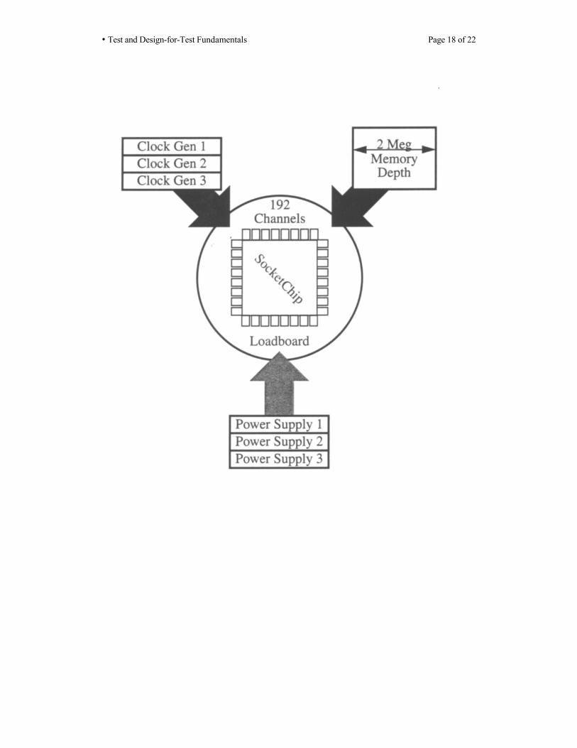
Automatic Test Equipment Integrated Circuit Automatic Test Equipment, also known as IC ATE, is generally a very
expensive (i.e., greater than $1,000,000.00) test platform. The ATE can be modeled or repre-sented as a number of channels with memory depth (a channel basically representing the memory behind a package pin), a number of clock generators, and a number of power supplies (see Figure 1-9). These resources are applied to the chip through a loadboard that houses the chip socket. Some other resources or functions may exist, such as:
- memory test functions (MTF's) to conduct algorithmic memory tests - analog-to-digital (ADC) and digital-to-analog (DAC) converters - current measurement devices for Idd and Iddq testing - frequency counters to verify or synchronize output clock signals The cost drivers of ATE are mostly related to the number of channels, the amount of
memory depth. the frequency of operation, and the accuracy of measurement.
ATE Limitations ATE is not exactly the same as a simulator. A simulator can operate with or without tim-
ing, can be cycle-based or event driven, and can access any signal, variable, or constant in a design. The waveforms applied by a simulator can be viewed as the ideal mathematical repre-sentation of a signal, unknown signals can be represented as a logical construct known as the "X;' and the high impedance state can be represented as the logical construct known as the "Z."
The ATE, on the other hand, can operate only at the edge of the design through the pack-age pins, and has real signal and clock delays and signal degradations, chip output loads, load board transmission line and round trip signal timing, and thermal considerations. The tester also has signal edge placement precision, accuracy, and edge-rate (rise and fall time) limitations.
ATE Cost Considerations The main component of the "cost-of-test" is the time a chip spends "in-socket" on the
ATE. There is a minimum cost based on the minimum time that it takes an automated handler to insert and remove a chip from the tester socket (production throughput). Aggressive handler time is generally in the 1-3 second range. Cost reductions to bring tester time below the handler threshold require testing multiple die in parallel with the same tester.
If the test programs applied on the tester are excessively complex or contain an excessive amount of vector data, then a vector reload may be required. A reload adds a large amount of time to the overall test process, which increases the "in-socket" time, and therefore, the cost of test. The ways to minimize the test program complexity and data size are to apply simplifying techniques, such as single-edge-set testing, and to apply vector compression to the vectors sets. A simpler test program also reduces the complexity of the ATE that is required. A less complex ATE requirement means that a less expensive tester can be used.

• Test and Design-for-Test Fundamentals Page 20 of 22
(Chip Point of View)
1. Input Setup time the signal must 2. Input Hold
Time: and be stable before the
clock
edge to ensure capture3. Output Valid Time:
stable after the clock edge
to ensure that capture is stable4. Output Hold
Time: valid (or tristated) and
stable on
the output after the clock available after output valid
Figure 1-10 Pin Timing
Test and Pin Timing
Tester and Device Pin Timing The tester must apply input stimulus to the input pins of the IC package, and must measure
or strobe the output response, with a known relationship to a reference. The most general form of reference is the clock signal(s) created by the tester and applied to the device-under-test as the system clock(s). The application of input stimulus and the measurement of response data with respect to the reference is generally known as pin timing (see Figure 1-10).

• Test and Design-for-Test Fundamentals Page 21 of 22
Sometimes the device under test has an internal clock generator (e.g., PLL), and the tester must align the application of input information and the measurement of output information against a clock-out signal from the chip itself. Since the timing relationship between the package pins, the internal logic, and the tester can be very subtle, and the accuracy and precision and lim-itations of the tester must be factored into the analysis, sometimes a tester must conduct an extensive edge search and update a variable timing table to ensure that applications and mea-surements with respect to the clock are accomplished within the stated specifications. This type of operation consumes test time and can be very costly as compared to referencing timing speci-fications from a tester generated clock (a "clock in" reference).
Tester Edge Sets The cost-of-test is lower if the test process requires the support of fewer edge sets (the
maximum optimization occurs if all testing can be done with only one edge set). The timing point, with respect to the reference, at which new information is applied to a device-under-test input pin, or at which response data is observed on a device-under-test output pin, establishes a timing edge set. If a package pin supports multiple application or strobe times or if the package pins support application or strobe time based on multiple references (e.g., clocks), then that pin is said to require more than one edge set. Another way of saying this is if the tester must support more than one timing standard or waveform to conduct testing, then this is another edge set.
An edge set is not just the pin timing standard, but also may include the tester timing for-mat. The tester timing format has to do with the way the tester generates or manages the signal. Single edge set testing generally means that data is applied, or measured, on a pin with the same timing standard and the same tester format throughout the test program.
Device Pin Timing Requirements The device-under-test must have the vectors applied from the tester based on the chip's own
timing limitations or specifications related to its input pins, output pins, and clock reference signals. These specifications are described in the chip's User Manual or Specification Data Sheet and represent such items as: the timing point associated with the application time that a stable signal must be applied to input pins with respect to the upcoming clock edge to ensure that it will be correctly captured by sequential elements within the part; or the timing point at which data exiting output pins will be stable and valid with respect to the previous clock edge.
Tester Pin Timing Formats Tester pin timing formats (see Figure 1-10) are a way for testers to easily generate
digital signals and represent them in the test program. These formats also inherently represent the concepts of "print on change;' or "print on time." For example, one way to represent pin data is to represent it as a "Non-Return"- format-this format emulates the print-on-change format in that the pin data changes value only when the data really changes, even if it is several clock cycles before the data changes. As a contrast, a "Return" format will always return the pin data value back to some default value at the end of the reference signal interval (representing the print-on-time format).
• Test and Design-for-Test Fundamentals Page 22 of 22
Tester Precision and Accuracy in Timing The tester itself provides a limitation to validating the timing of the chip-under-test. This
is the tester's ability to resolve timing measurements or applications, and the ability to place the edges used as data and reference.
Precision: The smallest measurement that the tester can resolve.
Accuracy: The smallest ambiguity in edge placement.
Summary The purpose of design-for-test is to embed the highest performance and most costly
electronics into the die to enable the ability to conduct accurate and low-cost quality measurement. DFT, if implemented efficiently, will enable quality to goals to be met within the cost of test budget, and enable vector automation to meeting aggressive time to market and time to volume manufacturing plans.
To Learn More To learn more about these topics, the following reading is recommended:
Crouch, Alfred L., Design for Test for Digital Ic's and Embedded Core SystemsPublisher: Prentice Hall PTR; 1st edition (June 15, 1999) ISBN: 0130848271
Abromovici, Miron, Melvin A. Breuer, Arthur D. Friedman. Digital Systems Testing and Testable
Design. New York: Computer Science Press. 1990. Dillinger, Thomas E. VLSI Engineering. Englewood Cliffs, NJ: Prentice Hall, 1988.
Gulati, Ravi K. and Charles F. Hawkins, eds. IDDQ Testing of VLSI Circuits A Special Issue of Journal of
Electronic Testing: Theory and Applications. Norwell, MA: Kluwer Academic Press, 1995. IEEE Standard Tests Access Port and Boundary-Scan Architecture. IEEE Standard 1149.1
1990. New York:IEEE Standards Board, 1990.
Parker, Kenneth P. The Boundary-Scan Handbook, 2nd Edition, Analog and Digital. Norwell, MA: Kluwer Academic Publishers, 1998
Tsui, Frank F.1SI/VLSI Testability Design. New York: McGraw-Hill, 1987.
Author, author: Mr. Crouch is responsible for research and the generation of development plans for new DFT methodologies, as well as providing
technical consultancy to semiconductor companies who are pursuing DFT test methodologies. Prior to joining Inovys, Al was a Principal Member of Technical Staff and DFT Manager for the Embedded Platform Solutions Organization at Motorola. Al's 20 years of experience in semiconductor design and test has also included DEC and Texas Instruments. During his career, Al has advocated improvements in test strategies in which he holds 13 patents. He is the widely read author of Design-For-Test For Digital IC's and Embedded Core Systems, in addition to many articles published in EE Times, and IEEE Design & Test. Al has frequently contributed to the International Test Conference as Presenter, Panel Member, Session Chair, and Paper Reviewer of DFT methodologies. Al has been a lecturer at University of New Mexico and at University of Texas as well as the Tutorial Session at the Design Automation Conference