1n4148w bav16w t4 t6 - hytic.net mount package ideally suited for automatic insertion . z. ... high...
TRANSCRIPT
JIANGSU CHANGJIANG ELECTRONICS TECHNOLOGY CO., LTD
SOD-123 Plastic-Encapsulate
www.cj-elec.com 1 B,Jul,2014
Diodes
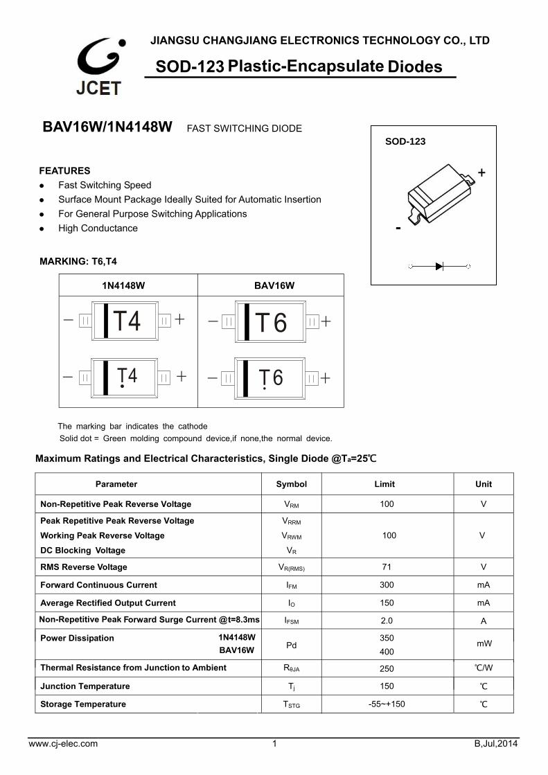
SOD-123
The marking bar indicates the cathode Solid dot = Green molding compound device,if none,the normal device.
BAV16W/1N4148W FAST SWITCHING DIODE
FEATURES
Fast Switching Speed Surface Mount Package Ideally Suited for Automatic Insertion For General Purpose Switching Applications High Conductance
MARKING: T6,T4
T4
T4
1N4148W
T6
T6
Maximum Ratings and Electrical Characteristics, Single Diode @Ta=25
Parameter Symbol Limit Unit
Non-Repetitive Peak Reverse Voltage VRM 100 V
Peak Repetitive Peak Reverse Voltage
Working Peak Reverse Voltage
DC Blocking Voltage
VRRM
VRWM
VR
100 V
RMS Reverse Voltage VR(RMS) 71 V
Forward Continuous Current IFM 300 mA
Average Rectified Output Current IO 150 mA
Forward Surge Current @t=8.3ms IFSM 2.0 A
Power Dissipation Pd
350 mW
Thermal Resistance from Junction to Ambient RθJA 250 /W
Junction Temperature Tj 150
Storage Temperature TSTG -55~+150
BAV16W
Non-Repetitive Peak
1N4148WBAV16W 400

www.cj-elec.com 2 B,Jul,2014
ELECTRICAL CHARACTERISTICS
Electrical Ratings @Ta=25
Parameter Symbol Min Typ Max Unit Conditions
VF1 0.715 V IF=1mA
VF2 0.855 V IF=10mA
VF3 1.0 V IF=50mA Forward voltage
VF4 1.25 V IF=150mA
IR1 1 μA VR=75V Reverse current
IR2 25 nA VR=20V
Capacitance between terminals CT 2 pF VR=0V,f=1MHz
Reverse recovery time trr 4 ns IF=IR=10mA
Irr=0.1XIR,RL=100Ω

www.cj-elec.com 3 B,Jul,2014
Typical Characteristics
0 4 8 12 16 200.6
0.8
1.0
1.2
1.4
1.6
0 25 50 75 100 125 1500
100
200
300
400
500
0.0 0.4 0.8 1.2 1.60.1
1
10
100
0 20 40 60 80 1001
10
100
1000
10000
Ta=25
f=1MHz
Capacitance Characteristics
REVERSE VOLTAGE VR (V)
CA
PA
CIT
AN
CE
BE
TW
EE
N T
ER
MIN
ALS
CT
(p
F)
1N4148W
Power Derating Curve
PO
WE
R D
ISS
IPA
TIO
N
P
D
(m
W)
AMBIENT TEMPERATURE Ta ( )
BAV16W
0.3
3
30
300
3
30
300
3000
Forward Characteristics
T a=1
00
T a=2
5
FO
RW
AR
D C
UR
RE
NT
I F
(m
A)
FORWARD VOLTAGE VF (V)
Reverse Characteristics
Ta=100
Ta=25
RE
VE
RS
E C
UR
RE
NT
I R
(nA
)
REVERSE VOLTAGE VR (V)
www.cj-elec.com 4 B,Jul,2014
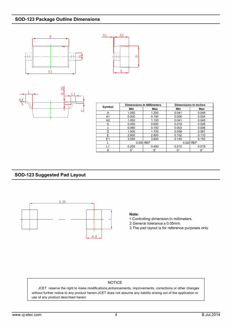
SOD-123 Package Outline Dimensions
SOD-123 Suggested Pad Layout
Min Max Min MaxA 1.050 1.250 0.041 0.049
A1 0.000 0.100 0.000 0.004A2 1.050 1.150 0.041 0.045b 0.450 0.650 0.018 0.026c 0.080 0.150 0.003 0.006D 1.500 1.700 0.059 0.067E 2.600 2.800 0.102 0.110
E1 3.550 3.850 0.140 0.152L
L1 0.250 0.450 0.010 0.018θ 0° 8° 0° 8°
0.500 REF 0.020 REF
Symbol Dimensions In Millimeters Dimensions In Inches

www.cj-elec.com 5 B,Jul,2014
SOD-123 Tape and Reel