2- to 8-phase vrm 10/9.1 pwm controllers with precise ... max8525 (vrm 10/vrd 10)/max8524 (vrm 9.1/...
TRANSCRIPT
General DescriptionThe MAX8525 (VRM 10/VRD 10)/MAX8524 (VRM 9.1/VRD 9.1) current-mode step-down controllers, theMAX8523 high-speed, dual-phase MOSFET gate driver,and the MAX8552 wide-input, single-phase MOSFETgate driver provide flexible, low-cost, low-voltage CPUcore supplies. The MAX8523 and MAX8552 high-speed,high-current gate drivers allow operation at high switch-ing frequencies to reduce external component size andcost for small-footprint, low-profile designs. Pin-selec-table 2-, 3-, and 4-phase operation and master-slave 6-and 8-phase operation provide output-current scalabilityfor servers, workstations, desktops, desk notes, and net-working applications. The switching frequency of the MAX8524/MAX8525 isadjustable from 150kHz to 1.2MHz, permitting loopbandwidths of up to 200kHz. Peak current-mode con-trol provides fast transient response and reduces cost.A proprietary current-sharing scheme reduces currentimbalance between phases to less than 5% at full load.The MAX8524/MAX8525 offer 0.4% initial accuracy andremote-sense functionality. Both controllers also featureprogrammable no-load offset and output-voltage posi-tioning to adjust the output voltage as a function of theoutput current. The fast-active voltage positioning furtherreduces bulk output capacitors and cost.Current-mode control also simplifies compensation witha variety of capacitors by eliminating the output-filterdouble pole associated with voltage-mode controllers.Both devices are compatible with electrolytic, tantalum,polymer, and ceramic capacitors. Output current sens-ing eliminates issues associated with controllers thatuse high-side current sense and ensure stable and jit-ter-free operation. Temperature-compensated, losslessinductor current sense eliminates the need for a cur-rent-sense resistor and further reduces cost, whilemaintaining voltage-positioning accuracy and reducingpower dissipation.The MAX8525 features control VID voltage transition fordynamic VID changes and eliminate both undervoltageand overvoltage overshoot. The PWRGD signal is accu-rate during VID code changes for the MAX8525 toavoid any false fault signal.Adjustable foldback current-limit and overvoltage pro-tection provide for a robust design.
ApplicationsServers, WorkstationsDesktop ComputersDesk Notes and LCD PCsVoltage-Regulator ModulesHigh-End Switches and Routers
Features♦ VRD/VRM 10 (MAX8525)♦ VRD/VRM 9.1 (MAX8524)♦ Fastest Load-Transient Response♦ Rapid-Active Average Current Sensing
Better than 5% Current BalanceFastest Voltage Positioning
♦ ±0.4% Initial Output-Voltage Accuracy♦ Pin-Selectable 2-/3-/4-Phase Operation♦ Master-Slave 6-/8-Phase Operation♦ Differential Remote Voltage Sensing♦ Dynamic VID Change (MAX8525)♦ Adjustable, Foldback Current Limit♦ Soft-Start and Soft-Stop♦ Power-Good Output♦ 150kHz to 1.2MHz Switching Frequency per Phase♦ 28-Lead QSOP Package
MA
X8
52
4/M
AX
85
25
2- to 8-Phase VRM 10/9.1 PWM Controllers with Precise Current Sharing and Fast Voltage
Positioning
________________________________________________________________ Maxim Integrated Products 1
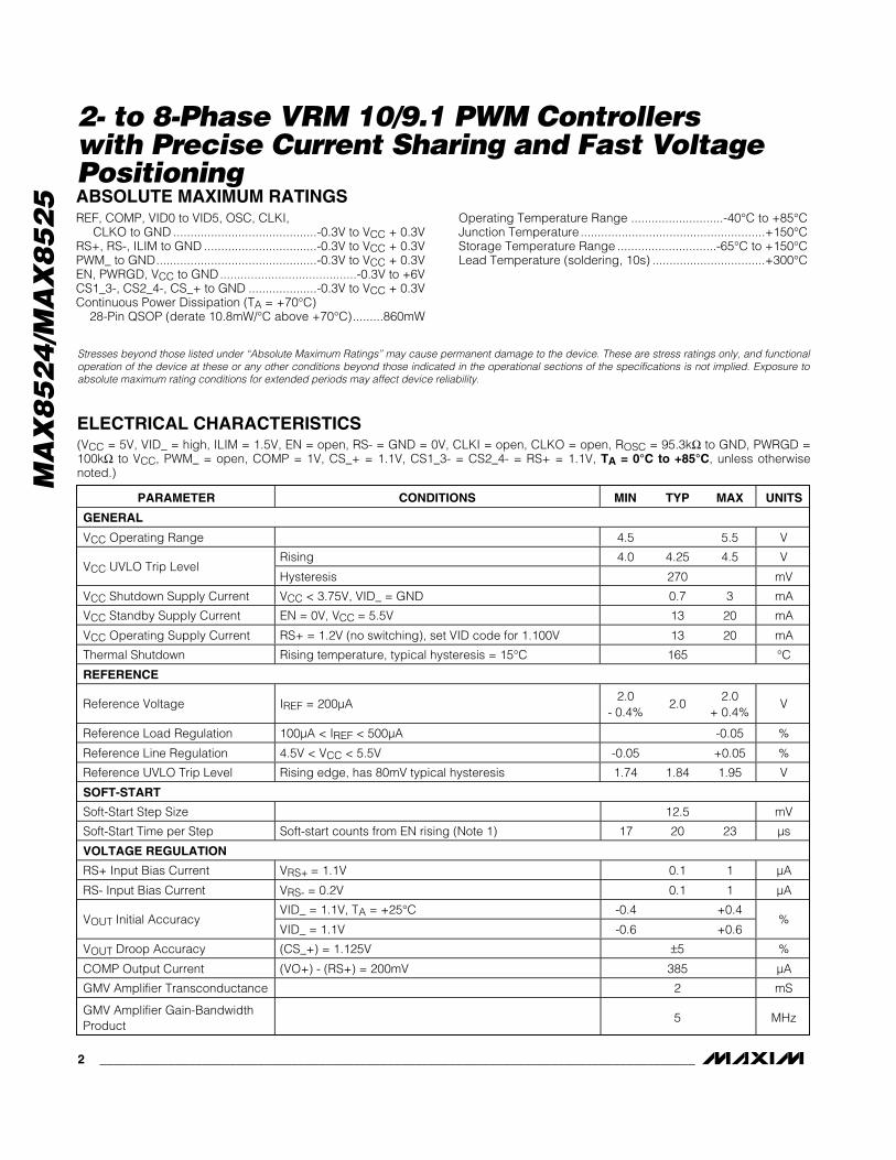
Pin Configurations
Ordering Information
19-2855; Rev 2; 4/05
For pricing, delivery, and ordering information, please contact Maxim/Dallas Direct! at 1-888-629-4642, or visit Maxim’s website at www.maxim-ic.com.
PART TEMP RANGE PIN-PACKAGE
MAX8524EEI -40°C to +85°C 28 QSOP
MAX8524EEI+ -40°C to +85°C 28 QSOP
MAX8525EEI -40°C to +85°C 28 QSOP
MAX8525EEI+ -40°C to +85°C 28 QSOP
Functional Diagram appears at end of data sheet.
28
27
26
25
24
23
22
21
20
19
18
17
16
15
1
2
3
4
5
6
7
8
9
10
11
12
13
14
PWM2
PWM4
CS4+
CS2_4-
CS2+
RS+
VID5
RS-
EN
VID4
VID3
VID2
VID1
VID0
CLKI
CLKO
PWRGD
OSC
ILIM
REF
COMP
GND
VCC
CS3+
CS1_3-
CS1+
PWM1
PWM3
QSOP
TOP VIEW
MAX8525
Pin Configurations continued at end of data sheet.
+Denotes lead-free package.
MA
X8
52
4/M
AX
85
25
2- to 8-Phase VRM 10/9.1 PWM Controllers with Precise Current Sharing and Fast VoltagePositioning
2 _______________________________________________________________________________________
ABSOLUTE MAXIMUM RATINGS
Stresses beyond those listed under “Absolute Maximum Ratings” may cause permanent damage to the device. These are stress ratings only, and functionaloperation of the device at these or any other conditions beyond those indicated in the operational sections of the specifications is not implied. Exposure toabsolute maximum rating conditions for extended periods may affect device reliability.
REF, COMP, VID0 to VID5, OSC, CLKI, CLKO to GND ..........................................-0.3V to VCC + 0.3V
RS+, RS-, ILIM to GND .................................-0.3V to VCC + 0.3VPWM_ to GND...............................................-0.3V to VCC + 0.3VEN, PWRGD, VCC to GND........................................-0.3V to +6VCS1_3-, CS2_4-, CS_+ to GND ....................-0.3V to VCC + 0.3VContinuous Power Dissipation (TA = +70°C)
28-Pin QSOP (derate 10.8mW/°C above +70°C).........860mW
Operating Temperature Range ...........................-40°C to +85°CJunction Temperature ......................................................+150°CStorage Temperature Range .............................-65°C to +150°CLead Temperature (soldering, 10s) .................................+300°C
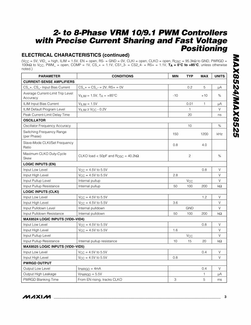
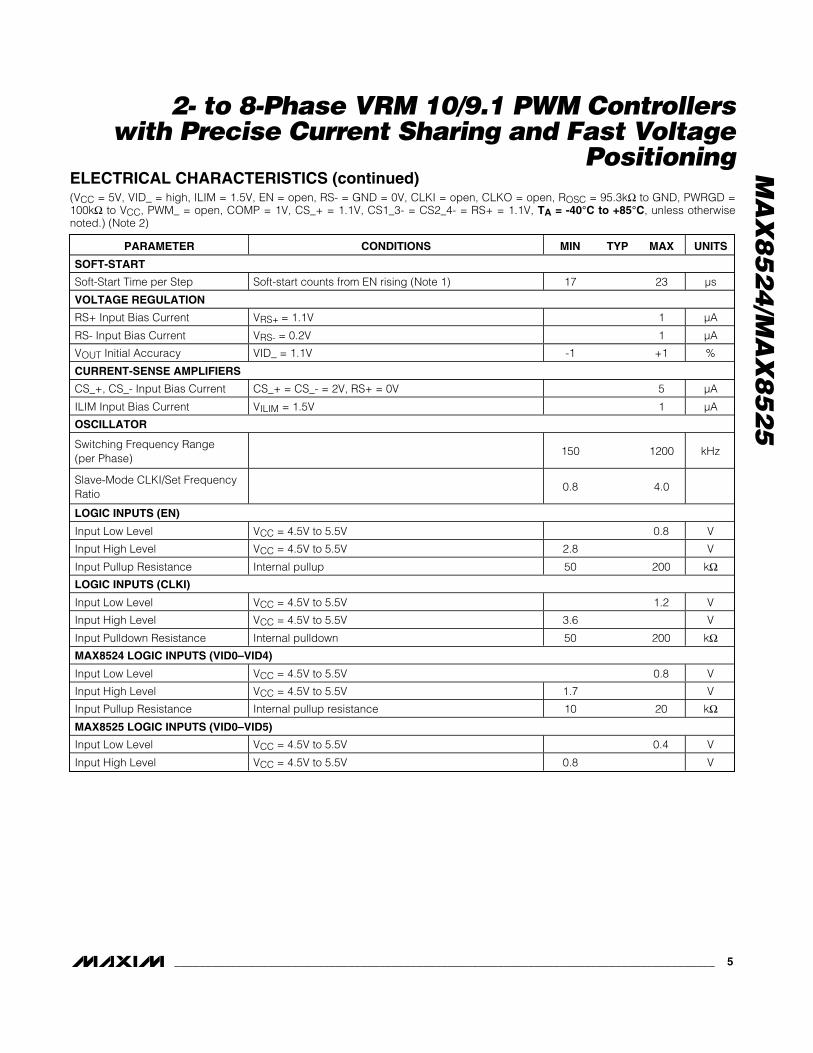
ELECTRICAL CHARACTERISTICS(VCC = 5V, VID_ = high, ILIM = 1.5V, EN = open, RS- = GND = 0V, CLKI = open, CLKO = open, ROSC = 95.3kΩ to GND, PWRGD =100kΩ to VCC, PWM_ = open, COMP = 1V, CS_+ = 1.1V, CS1_3- = CS2_4- = RS+ = 1.1V, TA = 0°C to +85°C, unless otherwisenoted.)
PARAMETER CONDITIONS MIN TYP MAX UNITS
GENERAL
VCC Operating Range 4.5 5.5 V
Rising 4.0 4.25 4.5 VVCC UVLO Trip Level
Hysteresis 270 mV
VCC Shutdown Supply Current VCC < 3.75V, VID_ = GND 0.7 3 mA
VCC Standby Supply Current EN = 0V, VCC = 5.5V 13 20 mA
VCC Operating Supply Current RS+ = 1.2V (no switching), set VID code for 1.100V 13 20 mA
Thermal Shutdown Rising temperature, typical hysteresis = 15°C 165 °C
REFERENCE
Reference Voltage IREF = 200µA2.0
- 0.4%2.0
2.0+ 0.4%
V
Reference Load Regulation 100µA < IREF < 500µA -0.05 %
Reference Line Regulation 4.5V < VCC < 5.5V -0.05 +0.05 %
Reference UVLO Trip Level Rising edge, has 80mV typical hysteresis 1.74 1.84 1.95 V
SOFT-START
Soft-Start Step Size 12.5 mV
Soft-Start Time per Step Soft-start counts from EN rising (Note 1) 17 20 23 µs
VOLTAGE REGULATION
RS+ Input Bias Current VRS+ = 1.1V 0.1 1 µA
RS- Input Bias Current VRS- = 0.2V 0.1 1 µA
VID_ = 1.1V, TA = +25°C -0.4 +0.4VOUT Initial Accuracy
VID_ = 1.1V -0.6 +0.6%
VOUT Droop Accuracy (CS_+) = 1.125V ±5 %
COMP Output Current (VO+) - (RS+) = 200mV 385 µA
GMV Amplifier Transconductance 2 mS
GMV Amplifier Gain-BandwidthProduct
5 MHz
MA
X8
52
4/M
AX
85
25
2- to 8-Phase VRM 10/9.1 PWM Controllers with Precise Current Sharing and Fast Voltage
Positioning
_______________________________________________________________________________________ 3
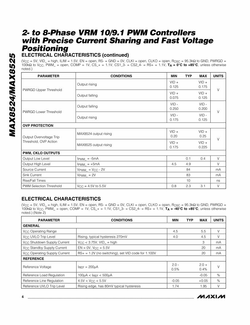
PARAMETER CONDITIONS MIN TYP MAX UNITS
CURRENT-SENSE AMPLIFIERS
CS_+, CS_- Input Bias Current CS_+ = CS_- = 2V, RS+ = 0V 0.2 5 µA
Average Current-Limit Trip LevelAccuracy
VILIM = 1.5V, TA = +85°C -10 +10 %
ILIM Input Bias Current VILIM = 1.5V 0.01 1 µA
ILIM Default Program Level VILIM ≥ VCC - 0.2V 1 V
Peak Current-Limit Delay Time 20 ns
OSCILLATOR
Oscillator Frequency Accuracy 10 %
Switching Frequency Range(per Phase)
150 1200 kHz
Slave-Mode CLKI/Set FrequencyRatio
0.8 4.0
Maximum CLKO Duty-CycleSkew
CLKO load < 50pF and ROSC = 40.2kΩ 2 %
LOGIC INPUTS (EN)
Input Low Level VCC = 4.5V to 5.5V 0.8 V
Input High Level VCC = 4.5V to 5.5V 2.8 V
Input Pullup Level Internal pullup VCC V
Input Pullup Resistance Internal pullup 50 100 200 kΩLOGIC INPUTS (CLKI)
Input Low Level VCC = 4.5V to 5.5V 1.2 V
Input High Level VCC = 4.5V to 5.5V 3.6 V
Input Pulldown Level Internal pulldown GND V
Input Pulldown Resistance Internal pulldown 50 100 200 kΩMAX8524 LOGIC INPUTS (VID0–VID4)
Input Low Level VCC = 4.5V to 5.5V 0.8 V
Input High Level VCC = 4.5V to 5.5V 1.6 V
Input Pullup Level VCC V
Input Pullup Resistance Internal pullup resistance 10 15 20 kΩMAX8525 LOGIC INPUTS (VID0–VID5)
Input Low Level VCC = 4.5V to 5.5V 0.4 V
Input High Level VCC = 4.5V to 5.5V 0.8 V
PWRGD OUTPUT
Output Low Level IPWRGD = 4mA 0.4 V
Output High Leakage VPWRGD = 5.5V 1 µA
PWRGD Blanking Time From EN rising, tracks CLKO 3 5 ms
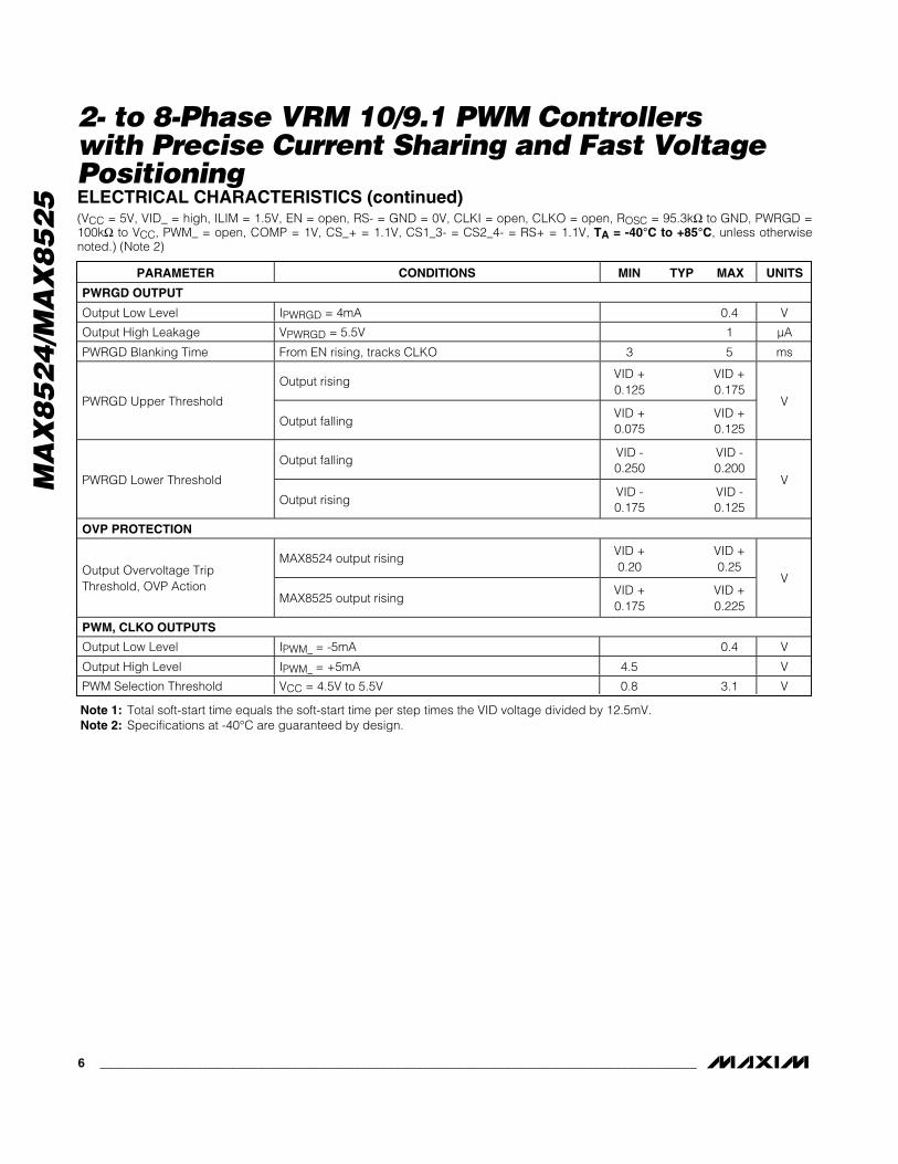
ELECTRICAL CHARACTERISTICS (continued)(VCC = 5V, VID_ = high, ILIM = 1.5V, EN = open, RS- = GND = 0V, CLKI = open, CLKO = open, ROSC = 95.3kΩ to GND, PWRGD =100kΩ to VCC, PWM_ = open, COMP = 1V, CS_+ = 1.1V, CS1_3- = CS2_4- = RS+ = 1.1V, TA = 0°C to +85°C, unless otherwisenoted.)
MA
X8
52
4/M
AX
85
25
2- to 8-Phase VRM 10/9.1 PWM Controllers with Precise Current Sharing and Fast VoltagePositioning
4 _______________________________________________________________________________________
PARAMETER CONDITIONS MIN TYP MAX UNITS
Output risingVID +0.125
VID +0.175
PWRGD Upper Threshold
Output fallingVID +0.075
VID +0.125
V
Output fallingVID -0.250
VID -0.200
PWRGD Lower Threshold
Output risingVID -0.175
VID -0.125
V
OVP PROTECTION
MAX8524 output risingVID +0.20
VID +0.25Output Overvoltage Trip
Threshold, OVP ActionMAX8525 output rising
VID +0.175
VID +0.225
V
PWM, CKLO OUTPUTS
Output Low Level IPWM_ = -5mA 0.1 0.4 V
Output High Level IPWM_ = +5mA 4.5 4.9 V
Source Current VPWM_ = VCC - 2V 84 mA
Sink Current VPWM_ = 2V 83 mA
Rise/Fall Times 10 ns
PWM Selection Threshold VCC = 4.5V to 5.5V 0.8 2.3 3.1 V
ELECTRICAL CHARACTERISTICS (continued)(VCC = 5V, VID_ = high, ILIM = 1.5V, EN = open, RS- = GND = 0V, CLKI = open, CLKO = open, ROSC = 95.3kΩ to GND, PWRGD =100kΩ to VCC, PWM_ = open, COMP = 1V, CS_+ = 1.1V, CS1_3- = CS2_4- = RS+ = 1.1V, TA = 0°C to +85°C, unless otherwisenoted.)
PARAMETER CONDITIONS MIN TYP MAX UNITS
GENERAL
VCC Operating Range 4.5 5.5 V
VCC UVLO Trip Level Rising, typical hysteresis 270mV 4.0 4.5 V
VCC Shutdown Supply Current VCC < 3.75V, VID_ = high 3 mA
VCC Standby Supply Current EN = 0V, VCC = 5.5V 20 mA
VCC Operating Supply Current RS+ = 1.2V (no switching), set VID code for 1.100V 20 mA
REFERENCE
Reference Voltage IREF = 200µA2.0 -0.5%
2.0 +0.4%
V
Reference Load Regulation 100µA < IREF < 500µA -0.05 %
Reference Line Regulation 4.5V < VCC < 5.5V -0.05 +0.05 %
Reference UVLO Trip Level Rising edge, has 80mV typical hysteresis 1.74 1.95 V
ELECTRICAL CHARACTERISTICS(VCC = 5V, VID_ = high, ILIM = 1.5V, EN = open, RS- = GND = 0V, CLKI = open, CLKO = open, ROSC = 95.3kΩ to GND, PWRGD =100kΩ to VCC, PWM_ = open, COMP = 1V, CS_+ = 1.1V, CS1_3- = CS2_4- = RS+ = 1.1V, TA = -40°C to +85°C, unless otherwisenoted.) (Note 2)
MA
X8
52
4/M
AX
85
25
2- to 8-Phase VRM 10/9.1 PWM Controllers with Precise Current Sharing and Fast Voltage
Positioning
_______________________________________________________________________________________ 5
PARAMETER CONDITIONS MIN TYP MAX UNITS
SOFT-START
Soft-Start Time per Step Soft-start counts from EN rising (Note 1) 17 23 µs
VOLTAGE REGULATION
RS+ Input Bias Current VRS+ = 1.1V 1 µA
RS- Input Bias Current VRS- = 0.2V 1 µA
VOUT Initial Accuracy VID_ = 1.1V -1 +1 %
CURRENT-SENSE AMPLIFIERS
CS_+, CS_- Input Bias Current CS_+ = CS_- = 2V, RS+ = 0V 5 µA
ILIM Input Bias Current VILIM = 1.5V 1 µA
OSCILLATOR
Switching Frequency Range(per Phase)
150 1200 kHz
Slave-Mode CLKI/Set FrequencyRatio
0.8 4.0
LOGIC INPUTS (EN)
Input Low Level VCC = 4.5V to 5.5V 0.8 V
Input High Level VCC = 4.5V to 5.5V 2.8 V
Input Pullup Resistance Internal pullup 50 200 kΩLOGIC INPUTS (CLKI)
Input Low Level VCC = 4.5V to 5.5V 1.2 V
Input High Level VCC = 4.5V to 5.5V 3.6 V
Input Pulldown Resistance Internal pulldown 50 200 kΩMAX8524 LOGIC INPUTS (VID0–VID4)
Input Low Level VCC = 4.5V to 5.5V 0.8 V
Input High Level VCC = 4.5V to 5.5V 1.7 V
Input Pullup Resistance Internal pullup resistance 10 20 kΩMAX8525 LOGIC INPUTS (VID0–VID5)
Input Low Level VCC = 4.5V to 5.5V 0.4 V
Input High Level VCC = 4.5V to 5.5V 0.8 V
ELECTRICAL CHARACTERISTICS (continued)(VCC = 5V, VID_ = high, ILIM = 1.5V, EN = open, RS- = GND = 0V, CLKI = open, CLKO = open, ROSC = 95.3kΩ to GND, PWRGD =100kΩ to VCC, PWM_ = open, COMP = 1V, CS_+ = 1.1V, CS1_3- = CS2_4- = RS+ = 1.1V, TA = -40°C to +85°C, unless otherwisenoted.) (Note 2)
MA
X8
52
4/M
AX
85
25
2- to 8-Phase VRM 10/9.1 PWM Controllers with Precise Current Sharing and Fast VoltagePositioning
6 _______________________________________________________________________________________
PARAMETER CONDITIONS MIN TYP MAX UNITS
PWRGD OUTPUT
Output Low Level IPWRGD = 4mA 0.4 V
Output High Leakage VPWRGD = 5.5V 1 µA
PWRGD Blanking Time From EN rising, tracks CLKO 3 5 ms
Output risingVID +0.125
VID +0.175
PWRGD Upper Threshold
Output fallingVID +0.075
VID +0.125
V
Output fallingVID -0.250
VID -0.200
PWRGD Lower Threshold
Output risingVID -0.175
VID -0.125
V
OVP PROTECTION
MAX8524 output risingVID +0.20
VID +0.25Output Overvoltage Trip
Threshold, OVP ActionMAX8525 output rising
VID +0.175
VID +0.225
V
PWM, CLKO OUTPUTS
Output Low Level IPWM_ = -5mA 0.4 V
Output High Level IPWM_ = +5mA 4.5 V
PWM Selection Threshold VCC = 4.5V to 5.5V 0.8 3.1 V
ELECTRICAL CHARACTERISTICS (continued)(VCC = 5V, VID_ = high, ILIM = 1.5V, EN = open, RS- = GND = 0V, CLKI = open, CLKO = open, ROSC = 95.3kΩ to GND, PWRGD =100kΩ to VCC, PWM_ = open, COMP = 1V, CS_+ = 1.1V, CS1_3- = CS2_4- = RS+ = 1.1V, TA = -40°C to +85°C, unless otherwisenoted.) (Note 2)
Note 1: Total soft-start time equals the soft-start time per step times the VID voltage divided by 12.5mV.Note 2: Specifications at -40°C are guaranteed by design.
MA
X8
52
4/M
AX
85
25
2- to 8-Phase VRM 10/9.1 PWM Controllers with Precise Current Sharing and Fast Voltage
Positioning
_______________________________________________________________________________________ 7
EFFICIENCY vs. LOAD CURRENTAT 1.45V OUTPUT
MAX
8524
toc0
1
LOAD CURRENT (A)
EFFI
CIEN
CY
10
10
20
30
40
50
60
70
80
90
100
01 100
VIN = 5V
VIN = 12V
OUTPUT VOLTAGE vs. LOAD CURRENT
MAX
8524
toc0
2
LOAD CURRENT (A)
V OUT
908010 20 30 50 6040 70
1.025
1.050
1.075
1.100
1.125
1.150
1.175
1.200
1.0000 100
VIN = 12V
OUTPUT LOAD TRANSIENTMAX8524 toc03
10μs
IOUT
VOUT50mV/div
POWER-GOODOUTPUT
0A
80A
4-PHASE ACTIVE CURRENT SHARING
MAX
8524
toc0
4
LOAD CURRENT (A)
INDU
CTOR
CUR
RENT
(A)
908070605040302010
5
10
15
20
25
00 100
DYNAMIC VID RESPONSE,250mV STEP VOLTAGE
MAX8524 toc05
40μs
POWER-GOODOUTPUT
PHASE 1INDUCTORCURRENT 10A/div
OUTPUTVOLTAGE200mV/div
SOFT-START WAVEFORMSAT 1.45V OUTPUT
MAX8524 toc06
1ms
ENABLEINPUT
INPUTCURRENT
0.5A/div
POWER-GOODOUTPUT
OUTPUTVOLTAGE0.5V/div
SOFT-STOP WAVEFORMSAT 1.45V OUTPUT
MAX8524 toc07
400μs
ENABLEINPUT
INPUTCURRENT
0.5A/div
POWER-GOODOUTPUT0A
OUTPUTVOLTAGE0.5V/div
IOUT = 0A
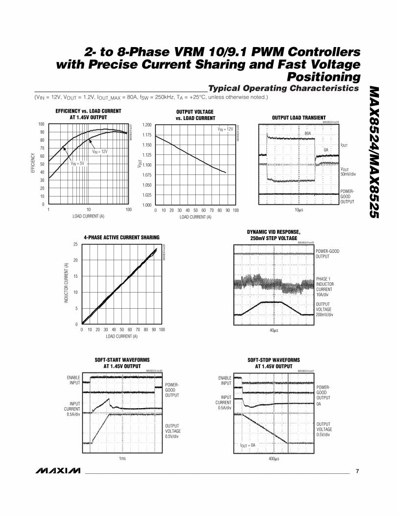
Typical Operating Characteristics(VIN = 12V, VOUT = 1.2V, IOUT_MAX = 80A, fSW = 250kHz, TA = +25°C, unless otherwise noted.)
MA
X8
52
4/M
AX
85
25
2- to 8-Phase VRM 10/9.1 PWM Controllers with Precise Current Sharing and Fast VoltagePositioning
8 _______________________________________________________________________________________
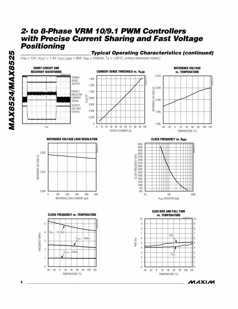
Typical Operating Characteristics (continued)(VIN = 12V, VOUT = 1.2V, IOUT_MAX = 80A, fSW = 250kHz, TA = +25°C, unless otherwise noted.)
CURRENT-SENSE THRESHOLD vs. VILIM
MAX
8524
toc1
0
OUTPUT CURRENT (A)
V ILI
M (V
)
908070605040302010
0.200
0.400
0.600
0.800
1.000
1.200
1.400
00 100
REFERENCE VOLTAGEvs. TEMPERATURE
MAX
8524
toc1
1
TEMPERATURE (°C)
REFE
RENC
E VO
LTAG
E (V
)
100806040200-20
1.995
2.000
2.005
2.010
1.990-40 120
REFERENCE VOLTAGE LOAD REGULATION
MAX
8524
toc1
2
REFERENCE LOAD CURRENT (μA)
REFE
RENC
E VO
LTAG
E (V
)
100 200 300 400
2.001
2.002
2.0000 500
CLOCK FREQUENCY vs. ROSC
MAX
8524
toc1
3
ROSC RESISTOR (kΩ)
CLOC
K FR
EQUE
NCY
(kHz
)
100
70010001300160019002200250028003100340037004000430046004900
40010 1000
CLOCK FREQUENCY vs. TEMPERATURE
MAX
8524
toc1
4
TEMPERATURE (°C)
FREQ
UENC
Y (M
Hz)
100806040200-20
1
2
3
4
5
0-40 120
ROSC = 43.2kΩ
ROSC = 105kΩ
ROSC = 294kΩ
CLKO RISE AND FALL TIMEvs. TEMPERATURE
MAX8524 toc15
TEMPERATURE (°C)
RISE
(ns)
12010060 800 20 40-20
1
2
3
4
5
6
7
8
9
10
0
1
2
3
4
5
6
7
8
9
10
0-40
FALL
RISE
SHORT-CIRCUIT ANDRECOVERY WAVEFORMS
MAX8524 toc09
1ms
POWER-GOODOUTPUT
PHASE 1INDUCTORCURRENT10A/div
OUTPUTVOLTAGE0.5V/div
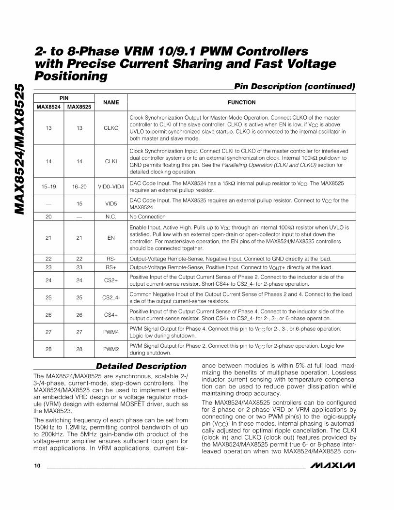
8-PHASE ACTIVE CURRENT SHARING
MAX
8524
toc1
7
LOAD CURRENT (A)
INDU
CTOR
CUR
RENT
(A)
150126101775226
5
10
15
20
25
00.193
MA
X8
52
4/M
AX
85
25
2- to 8-Phase VRM 10/9.1 PWM Controllers with Precise Current Sharing and Fast Voltage
Positioning
_______________________________________________________________________________________ 9
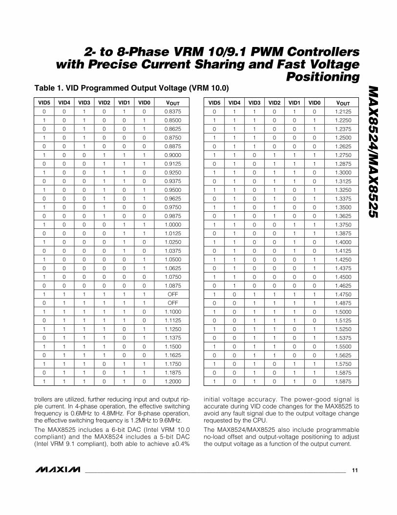
8-PHASE OPERATION: DYNAMIC VID RESPONSE
MAX8524 toc18
40μs
POWER-GOODOUTPUT
PHASE 1INDUCTORCURRENT10A/div
OUTPUT VOLTAGE200mV/div
Typical Operating Characteristics (continued)(VIN = 12V, VOUT = 1.2V, IOUT_MAX = 80A, fSW = 250kHz, TA = +25°C, unless otherwise noted.)
Pin Description
PIN
MAX8524 MAX8525NAME FUNCTION
1 1 PWM3 PWM Signal Output for Phase 3. Logic low during shutdown.
2 2 PWM1 PWM Signal Output for Phase 1. Logic low during shutdown
3 3 CS1+Positive Input of the Output Current Sense of Phase 1. Connect to the inductor side of theoutput current-sense resistor.
4 4 CS1_3-Common Negative Input of the Output Current Sense of Phases 1 and 3. Connect to the loadside of the output current-sense resistors.
5 5 CS3+Positive Input of the Output Current Sense of Phase 3. Connect to the inductor side of theoutput current-sense resistor.
6 6 VCC IC Supply Input. Bypass to GND with a ceramic capacitor of at least 1µF.
7 7 GND IC Ground. Single connection to system ground.
8 8 COMP
Error-Amplifier Output. Connect to a tap in a resistor-divider from REF to GND to set the finiteDC gain for active voltage positioning. Add a series RC network from COMP to GND tocompensate the control loop. For 6- or 8-phase operation, connect COMP pins of twocontrollers together for active current sharing.
9 9 REF2.0V ±0.4% Reference Output. Bypass REF to GND with a ≤2.2µF low-ESR capacitor. REFcan source 0.5mA for external loads. REF is alive when EN is low if VCC is above UVLO.
10 10 ILIMOutput Current-Limit Set. Connect to a tap of a resistor-divider from REF to GND to set thecycle-by-cycle average current-limit threshold. Current limit (per phase) = VILIM / (50 xRSENSE). Connect to VCC to set the default 20mV current-limit threshold.
11 11 OSCInternal Clock Oscillator Frequency-Set Input. Connect a resistor from OSC to GND to set theswitching frequency. OSC must be connected to an external resistor even if the IC is used inslave mode. This pin is operational in shutdown if VCC is above UVLO.
12 12 PWRGDOpen-Drain Power-Good Indicator. PWRGD pulls low until the output voltage is in regulation.PWRGD is low in shutdown and during UVLO.
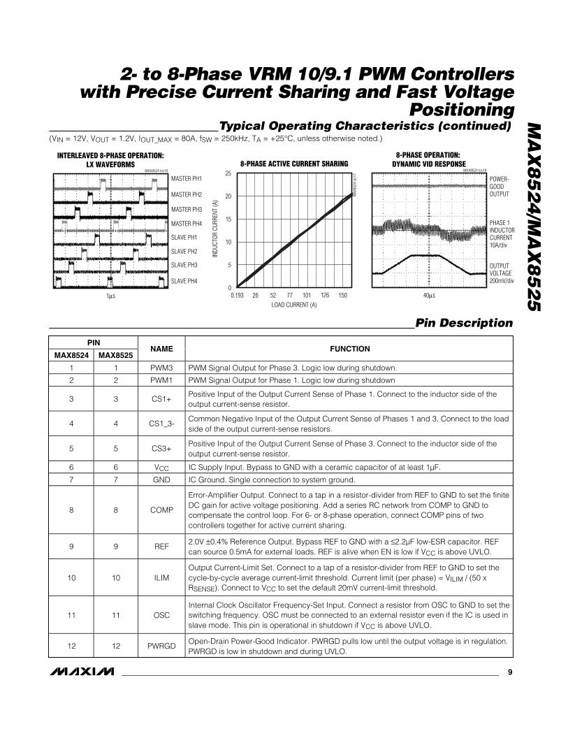
INTERLEAVED 8-PHASE OPERATION:LX WAVEFORMS
MAX8524 toc16
1μs
MASTER PH1
MASTER PH2
MASTER PH3
MASTER PH4
SLAVE PH1
SLAVE PH2
SLAVE PH3
SLAVE PH4
MA
X8
52
4/M
AX
85
25
Detailed DescriptionThe MAX8524/MAX8525 are synchronous, scalable 2-/3-/4-phase, current-mode, step-down controllers. TheMAX8524/MAX8525 can be used to implement eitheran embedded VRD design or a voltage regulator mod-ule (VRM) design with external MOSFET driver, such asthe MAX8523.
The switching frequency of each phase can be set from150kHz to 1.2MHz, permitting control bandwidth of upto 200kHz. The 5MHz gain-bandwidth product of thevoltage-error amplifier ensures sufficient loop gain formost applications. In VRM applications, current bal-
ance between modules is within 5% at full load, maxi-mizing the benefits of multiphase operation. Losslessinductor current sensing with temperature compensa-tion can be used to reduce power dissipation whilemaintaining droop accuracy.
The MAX8524/MAX8525 controllers can be configuredfor 3-phase or 2-phase VRD or VRM applications byconnecting one or two PWM pin(s) to the logic-supplypin (VCC). In these modes, internal phasing is automati-cally adjusted for optimal ripple cancellation. The CLKI(clock in) and CLKO (clock out) features provided bythe MAX8524/MAX8525 permit true 6- or 8-phase inter-leaved operation when two MAX8524/MAX8525 con-
10 ______________________________________________________________________________________
2- to 8-Phase VRM 10/9.1 PWM Controllers with Precise Current Sharing and Fast VoltagePositioning
Pin Description (continued)PIN
MAX8524 MAX8525NAME FUNCTION
13 13 CLKO
Clock Synchronization Output for Master-Mode Operation. Connect CLKO of the mastercontroller to CLKI of the slave controller. CLKO is active when EN is low, if VCC is aboveUVLO to permit synchronized slave startup. CLKO is connected to the internal oscillator inboth master and slave mode.
14 14 CLKI
Clock Synchronization Input. Connect CLKI to CLKO of the master controller for interleaveddual controller systems or to an external synchronization clock. Internal 100kΩ pulldown toGND permits floating this pin. See the Paralleling Operation (CLKI and CLKO) section fordetailed clocking operation.
15–19 16–20 VID0–VID4DAC Code Input. The MAX8524 has a 15kΩ internal pullup resistor to VCC. The MAX8525requires an external pullup resistor.
— 15 VID5DAC Code Input. The MAX8525 requires an external pullup resistor. Connect to VCC for theMAX8524.
20 — N.C. No Connection
21 21 EN
Enable Input, Active High. Pulls up to VCC through an internal 100kΩ resistor when UVLO issatisfied. Pull low with an external open-drain or open-collector input to shut down thecontroller. For master/slave operation, the EN pins of the MAX8524/MAX8525 controllersshould be connected together.
22 22 RS- Output-Voltage Remote-Sense, Negative Input. Connect to GND directly at the load.
23 23 RS+ Output-Voltage Remote-Sense, Positive Input. Connect to VOUT+ directly at the load.
24 24 CS2+Positive Input of the Output Current Sense of Phase 2. Connect to the inductor side of theoutput current-sense resistor. Short CS4+ to CS2_4- for 2-phase operation.
25 25 CS2_4-Common Negative Input of the Output Current Sense of Phases 2 and 4. Connect to the loadside of the output current-sense resistors.
26 26 CS4+Positive Input of the Output Current Sense of Phase 4. Connect to the inductor side of theoutput current-sense resistor. Short CS4+ to CS2_4- for 2-, 3-, or 6-phase operation.
27 27 PWM4PWM Signal Output for Phase 4. Connect this pin to VCC for 2-, 3-, or 6-phase operation.Logic low during shutdown.
28 28 PWM2PWM Signal Output for Phase 2. Connect this pin to VCC for 2-phase operation. Logic lowduring shutdown.
trollers are utilized, further reducing input and output rip-ple current. In 4-phase operation, the effective switchingfrequency is 0.6MHz to 4.8MHz. For 8-phase operation,the effective switching frequency is 1.2MHz to 9.6MHz.
The MAX8525 includes a 6-bit DAC (Intel VRM 10.0compliant) and the MAX8524 includes a 5-bit DAC(Intel VRM 9.1 compliant), both able to achieve ±0.4%
initial voltage accuracy. The power-good signal isaccurate during VID code changes for the MAX8525 toavoid any fault signal due to the output voltage changerequested by the CPU.
The MAX8524/MAX8525 also include programmableno-load offset and output-voltage positioning to adjustthe output voltage as a function of the output current.
MA
X8
52
4/M
AX
85
25
2- to 8-Phase VRM 10/9.1 PWM Controllers with Precise Current Sharing and Fast Voltage
Positioning
______________________________________________________________________________________ 11
VID5 VID4 VID3 VID2 VID1 VID0 VOUT
0 1 1 0 1 0 1.2125
1 1 1 0 0 1 1.2250
0 1 1 0 0 1 1.2375
1 1 1 0 0 0 1.2500
0 1 1 0 0 0 1.2625
1 1 0 1 1 1 1.2750
0 1 0 1 1 1 1.2875
1 1 0 1 1 0 1.3000
0 1 0 1 1 0 1.3125
1 1 0 1 0 1 1.3250
0 1 0 1 0 1 1.3375
1 1 0 1 0 0 1.3500
0 1 0 1 0 0 1.3625
1 1 0 0 1 1 1.3750
0 1 0 0 1 1 1.3875
1 1 0 0 1 0 1.4000
0 1 0 0 1 0 1.4125
1 1 0 0 0 1 1.4250
0 1 0 0 0 1 1.4375
1 1 0 0 0 0 1.4500
0 1 0 0 0 0 1.4625
1 0 1 1 1 1 1.4750
0 0 1 1 1 1 1.4875
1 0 1 1 1 0 1.5000
0 0 1 1 1 0 1.5125
1 0 1 1 0 1 1.5250
0 0 1 1 0 1 1.5375
1 0 1 1 0 0 1.5500
0 0 1 1 0 0 1.5625
1 0 1 0 1 1 1.5750
0 0 1 0 1 1 1.5875
1 0 1 0 1 0 1.5875
VID5 VID4 VID3 VID2 VID1 VID0 VOUT
0 0 1 0 1 0 0.8375
1 0 1 0 0 1 0.8500
0 0 1 0 0 1 0.8625
1 0 1 0 0 0 0.8750
0 0 1 0 0 0 0.8875
1 0 0 1 1 1 0.9000
0 0 0 1 1 1 0.9125
1 0 0 1 1 0 0.9250
0 0 0 1 1 0 0.9375
1 0 0 1 0 1 0.9500
0 0 0 1 0 1 0.9625
1 0 0 1 0 0 0.9750
0 0 0 1 0 0 0.9875
1 0 0 0 1 1 1.0000
0 0 0 0 1 1 1.0125
1 0 0 0 1 0 1.0250
0 0 0 0 1 0 1.0375
1 0 0 0 0 1 1.0500
0 0 0 0 0 1 1.0625
1 0 0 0 0 0 1.0750
0 0 0 0 0 0 1.0875
1 1 1 1 1 1 OFF
0 1 1 1 1 1 OFF
1 1 1 1 1 0 1.1000
0 1 1 1 1 0 1.1125
1 1 1 1 0 1 1.1250
0 1 1 1 0 1 1.1375
1 1 1 1 0 0 1.1500
0 1 1 1 0 0 1.1625
1 1 1 0 1 1 1.1750
0 1 1 0 1 1 1.1875
1 1 1 0 1 0 1.2000
Table 1. VID Programmed Output Voltage (VRM 10.0)
MA
X8
52
4/M
AX
85
25
Clock Frequency (OSC)The clock frequency of the MAX8524/MAX8525 is setby an external resistor from OSC to ground. Afterselecting the switching frequency per phase, fSW, andthe number of phases, using Table 3, select the clockfrequency. For 6- or 8-phase operation, connect anexternal resistor to OSC of both master and slave con-trollers even if the MAX8524/MAX8525 is operated in
slave mode. A 1% resistor is recommended for theROSC to maintain good frequency accuracy, and ROSCshould be placed as close as possible to the OSC pin.
Voltage Reference (REF)A precision 2V reference is provided by theMAX8524/MAX8525 at the REF pin. REF is capable ofsourcing up to 500µA for external loads. REF staysalive when EN is low and while VCC is above UVLO.Connect a 0.22µF ceramic capacitor from REF to GND.The capacitor should be placed as close to the REF pinas possible.
An internal REFOK monitors the reference voltage. Thereference voltage must be above the REFOK thresholdof 1.85V to activate the controller. The controller is dis-abled if the reference voltage falls below 1.81V.
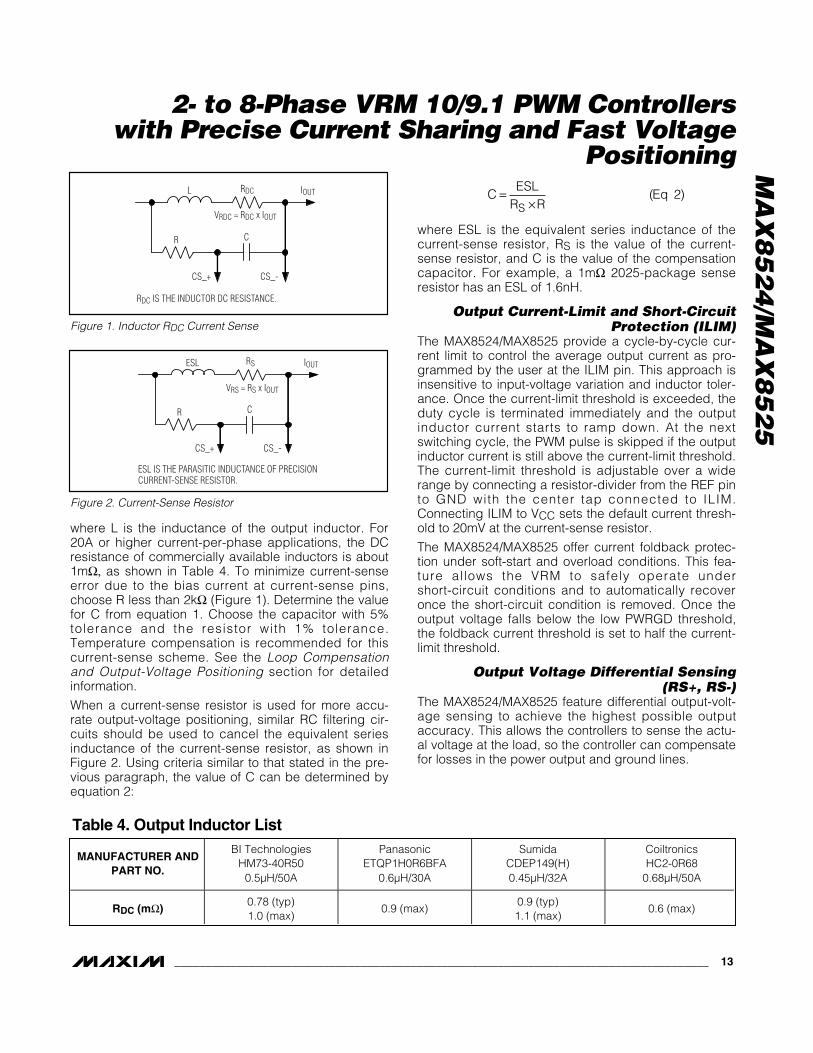
Output Current Sensing (CS_+, CS_-)The output current of each phase is sensed differential-ly with a shared common return for each phase pair. Alow offset voltage and high-gain (50V/V) differential cur-rent amplifier at each phase allow low-resistance cur-rent-sense resistors to be used to minimize powerdissipation. Sensing the current at the output of eachphase offers advantages, including less noise sensitivi-ty, more accurate current sharing between phases, andthe flexibility of using either a current-sense resistor orthe DC resistance of the output inductor.
Using the DC resistance, RDC, of the output inductorallows higher efficiency. In this configuration, the initialtolerance and temperature coefficient of RDC must beaccounted for in the output-voltage droop-error budget.An RC filtering network is needed to extract the currentinformation from the output inductor, as shown in Figure1. The time constant of the RC network is governed byequation 1:
RCL
REq
DC= ( )1
12 ______________________________________________________________________________________
2- to 8-Phase VRM 10/9.1 PWM Controllers with Precise Current Sharing and Fast VoltagePositioning
VID4 VID3 VID2 VID1 VID0 VOUT
0 0 0 0 0 1.850
0 0 0 0 1 1.825
0 0 0 1 0 1.800
0 0 0 1 1 1.775
0 0 1 0 0 1.750
0 0 1 0 1 1.725
0 0 1 1 0 1.700
0 0 1 1 1 1.675
0 1 0 0 0 1.650
0 1 0 0 1 1.625
0 1 0 1 0 1.600
0 1 0 1 1 1.575
0 1 1 0 0 1.550
0 1 1 0 1 1.525
0 1 1 1 0 1.500
0 1 1 1 1 1.475
1 0 0 0 0 1.450
1 0 0 0 1 1.425
1 0 0 1 0 1.400
1 0 0 1 1 1.375
1 0 1 0 0 1.350
1 0 1 0 1 1.325
1 0 1 1 0 1.300
1 0 1 1 1 1.275
1 1 0 0 0 1.250
1 1 0 0 1 1.225
1 1 0 1 0 1.200
1 1 0 1 1 1.175
1 1 1 0 0 1.150
1 1 1 0 1 1.125
1 1 1 1 0 1.100
1 1 1 1 1 Shutdown
Table 2. VID Programmed OutputVoltage (VRM 9.1)
NO. OF PHASES PIN CONNECTIONS fCLKO
2 PWM2 = PWM4 = VCC 4 x fSW
3 PWM4 = VCC 3 x fSW
4 — 4 x fSW
6 PWM4 = VCC 3 x fSW
8 — 4 x fSW
Table 3. Clock Frequency Setting vs. Switching Frequency and Number of Phases
2- to 8-Phase VRM 10/9.1 PWM Controllers with Precise Current Sharing and Fast Voltage
Positioning
where L is the inductance of the output inductor. For20A or higher current-per-phase applications, the DCresistance of commercially available inductors is about1mΩ, as shown in Table 4. To minimize current-senseerror due to the bias current at current-sense pins,choose R less than 2kΩ (Figure 1). Determine the valuefor C from equation 1. Choose the capacitor with 5%tolerance and the resistor with 1% tolerance.Temperature compensation is recommended for thiscurrent-sense scheme. See the Loop Compensationand Output-Voltage Positioning section for detailedinformation.
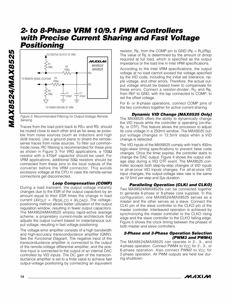
When a current-sense resistor is used for more accu-rate output-voltage positioning, similar RC filtering cir-cuits should be used to cancel the equivalent seriesinductance of the current-sense resistor, as shown inFigure 2. Using criteria similar to that stated in the pre-vious paragraph, the value of C can be determined byequation 2:
where ESL is the equivalent series inductance of thecurrent-sense resistor, RS is the value of the current-sense resistor, and C is the value of the compensationcapacitor. For example, a 1mΩ 2025-package senseresistor has an ESL of 1.6nH.
Output Current-Limit and Short-CircuitProtection (ILIM)
The MAX8524/MAX8525 provide a cycle-by-cycle cur-rent limit to control the average output current as pro-grammed by the user at the ILIM pin. This approach isinsensitive to input-voltage variation and inductor toler-ance. Once the current-limit threshold is exceeded, theduty cycle is terminated immediately and the outputinductor current starts to ramp down. At the nextswitching cycle, the PWM pulse is skipped if the outputinductor current is still above the current-limit threshold.The current-limit threshold is adjustable over a widerange by connecting a resistor-divider from the REF pinto GND with the center tap connected to ILIM.Connecting ILIM to VCC sets the default current thresh-old to 20mV at the current-sense resistor.
The MAX8524/MAX8525 offer current foldback protec-tion under soft-start and overload conditions. This fea-ture allows the VRM to safely operate undershort-circuit conditions and to automatically recoveronce the short-circuit condition is removed. Once theoutput voltage falls below the low PWRGD threshold,the foldback current threshold is set to half the current-limit threshold.
Output Voltage Differential Sensing (RS+, RS-)
The MAX8524/MAX8525 feature differential output-volt-age sensing to achieve the highest possible outputaccuracy. This allows the controllers to sense the actu-al voltage at the load, so the controller can compensatefor losses in the power output and ground lines.
CESL
R REq
S=
× ( )2
MA
X8
52
4/M
AX
85
25
______________________________________________________________________________________ 13
L RDC IOUT
VRDC = RDC x IOUT
R
RDC IS THE INDUCTOR DC RESISTANCE.
C
CS_+ CS_-
Figure 1. Inductor RDC Current Sense
ESL RS IOUT
VRS = RS x IOUT
R C
CS_+ CS_-
ESL IS THE PARASITIC INDUCTANCE OF PRECISIONCURRENT-SENSE RESISTOR.
Figure 2. Current-Sense Resistor
MANUFACTURER ANDPART NO.
BI TechnologiesHM73-40R50
0.5µH/50A
PanasonicETQP1H0R6BFA
0.6µH/30A
SumidaCDEP149(H)0.45µH/32A
CoiltronicsHC2-0R68
0.68µH/50A
RDC (mΩ)0.78 (typ)1.0 (max)
0.9 (max)0.9 (typ)1.1 (max)
0.6 (max)
Table 4. Output Inductor List
MA
X8
52
4/M
AX
85
25
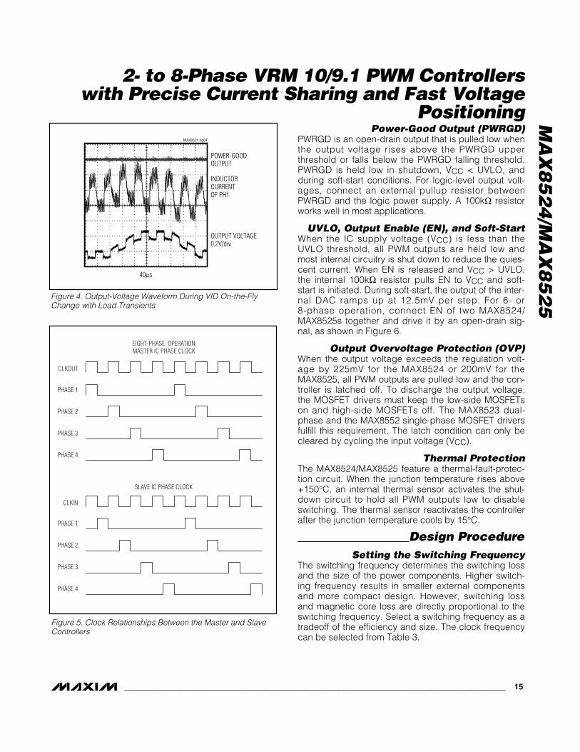
Traces from the load point back to RS+ and RS- shouldbe routed close to each other and as far away as possi-ble from noise sources (such as inductors and highdi/dt traces). Use a ground plane to shield the remote-sense traces from noise sources. To filter out common-mode noise, RC filtering is recommended for these pinsas shown in Figure 3. For VRD applications, a 100Ωresistor with a 470pF capacitor should be used. ForVRM applications, additional 50Ω resistors should beconnected from these pins to the local outputs of theconverter before the VRM connector. This avoidsexcessive voltage at the CPU in case the remote-senseconnections get disconnected.
Loop Compensation (COMP)During a load transient, the output voltage instantlychanges due to the ESR of the output capacitors by anamount equal to their ESR times the change in loadcurrent (ΔVOUT = -RESR_CO x ΔILOAD). The voltage-positioning method allows better utilization of the outputregulation window, resulting in fewer output capacitors.The MAX8524/MAX8525 employ rapid-active averagescheme, a proprietary current-mode architecture thatadjusts the output current based on instantaneous out-put voltage, resulting in fast voltage positioning.
The voltage-error amplifier consists of a high bandwidthand high-accuracy transconductance amplifier (GMV).See the Functional Diagram. The negative input of thetransconductance amplifier is connected to the outputof the remote-voltage differential amplifier, and the pos-itive input is connected to the output of an internal DACcontrolled by VID inputs. The DC gain of the transcon-ductance amplifier is set to a finite value to achieve fastoutput-voltage positioning by connecting an equivalent
resistor, RE, from the COMP pin to GND (RE = RU//RB).The value of RE is determined by the amount of drooprequired at full load, which is specified as the outputimpedance or the load line in Intel VRM specifications.
According to the Intel VRM specifications, the outputvoltage at no load cannot exceed the voltage specifiedby the VID code, including the initial set tolerance, rip-ple voltage, and other errors. Therefore, the actual out-put voltage should be biased lower to compensate forthese errors. Connect a resistor-divider, RU and RB,from REF to GND, with the tap connected to COMP, toset the offset voltage.
For 6- or 8-phase operations, connect COMP pins ofthe two controllers together for active current sharing.
Dynamic VID Change (MAX8525 Only)The MAX8525 offers the ability to dynamically changethe VID inputs while the controller is operating (on-the-fly, or OTF). This feature allows the processor to adjustits core voltage in a 250mV window. The MAX8525 out-put voltage changes in 12.5mV steps when a VIDchange is detected.
The VID inputs of the MAX8525 comply with Intel’s 400nslogic-skew timing specifications to prevent false codechanges. Once the timer expires, the controller starts tochange the DAC output. Figure 4 shows the output volt-age step during a VID OTF event. The MAX8525 con-troller accepts both step-by-step changes of VID inputsor all-at-once VID inputs changes. For all-at-once VIDinput changes, the output-voltage slew rate is the sameas 12.5mV per step and 2µs duration.
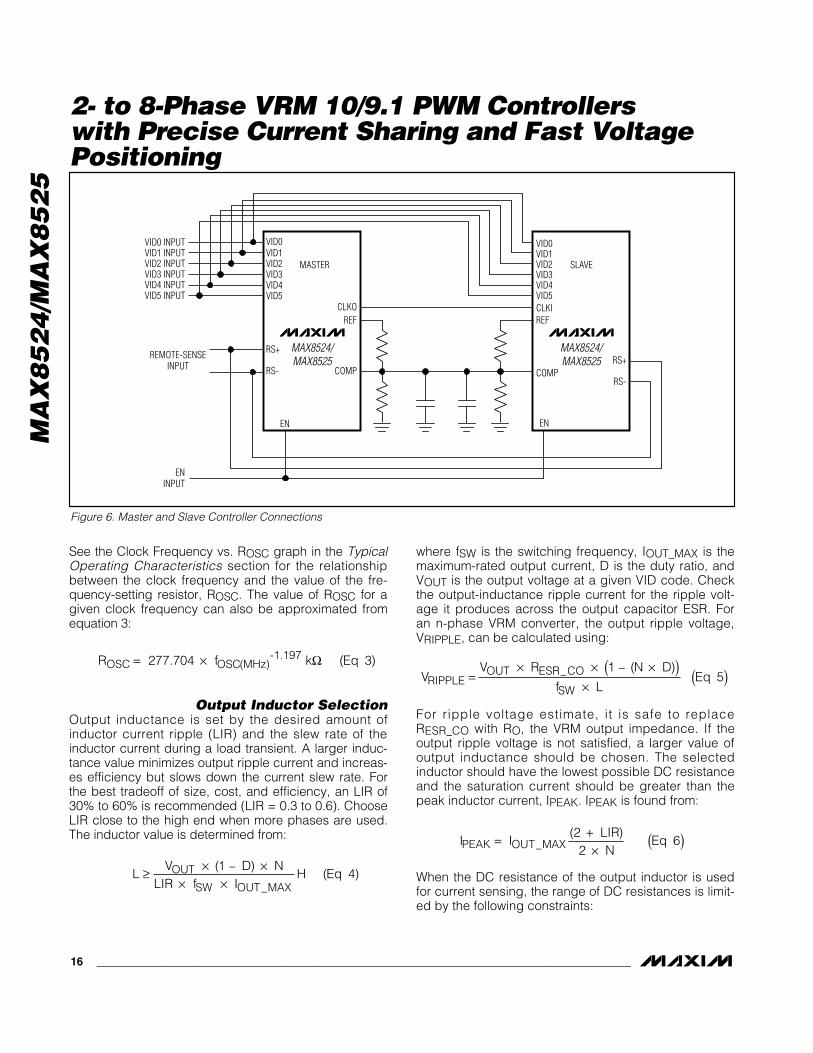
Paralleling Operation (CLKI and CLKO)Two MAX8524/MAX8525s can be connected togetherto generate 6-phase or 8-phase core supplies. In thisconfiguration, one MAX8524/MAX8525 serves as amaster and the other serves as a slave. Connect theCLKI pin of the slave controller to the CLKO pin of themaster controller. Interleaved operation is achieved bysynchronizing the master controller to the CLKO risingedge and the slave controller to the CLKO falling edge.Figure 5 shows the clock timing between the phases ofboth master and slave controllers.
2-Phase and 3-Phase Operation Selection(PWM3 and PWM4)
The MAX8524/MAX8525 can operate in 2-, 3-, and 4-phase operation. Connect PWM4 to VCC for 2-, 3-, or6-phase operation. Also connect PWM2 to VCC for 2-phase operation. All PWM outputs are held low dur-ing shutdown.
14 ______________________________________________________________________________________
2- to 8-Phase VRM 10/9.1 PWM Controllers with Precise Current Sharing and Fast VoltagePositioning
MAX8524/MAX8525
R3100Ω
R150Ω
R4100Ω
R250Ω C1
470pFC1470pF
TO POWER GROUND OF VRM
TO POSITIVE OUTPUT OF VRM
TO REMOTE-SENSE LOCATION
RS+
RS-
Figure 3. Recommended Filtering for Output-Voltage RemoteSensing
Power-Good Output (PWRGD)PWRGD is an open-drain output that is pulled low whenthe output voltage rises above the PWRGD upperthreshold or falls below the PWRGD falling threshold.PWRGD is held low in shutdown, VCC < UVLO, andduring soft-start conditions. For logic-level output volt-ages, connect an external pullup resistor betweenPWRGD and the logic power supply. A 100kΩ resistorworks well in most applications.
UVLO, Output Enable (EN), and Soft-StartWhen the IC supply voltage (VCC) is less than theUVLO threshold, all PWM outputs are held low andmost internal circuitry is shut down to reduce the quies-cent current. When EN is released and VCC > UVLO,the internal 100kΩ resistor pulls EN to VCC and soft-start is initiated. During soft-start, the output of the inter-nal DAC ramps up at 12.5mV per step. For 6- or8-phase operation, connect EN of two MAX8524/MAX8525s together and drive it by an open-drain sig-nal, as shown in Figure 6.
Output Overvoltage Protection (OVP)When the output voltage exceeds the regulation volt-age by 225mV for the MAX8524 or 200mV for theMAX8525, all PWM outputs are pulled low and the con-troller is latched off. To discharge the output voltage,the MOSFET drivers must keep the low-side MOSFETson and high-side MOSFETs off. The MAX8523 dual-phase and the MAX8552 single-phase MOSFET driversfulfill this requirement. The latch condition can only becleared by cycling the input voltage (VCC).
Thermal ProtectionThe MAX8524/MAX8525 feature a thermal-fault-protec-tion circuit. When the junction temperature rises above+150°C, an internal thermal sensor activates the shut-down circuit to hold all PWM outputs low to disableswitching. The thermal sensor reactivates the controllerafter the junction temperature cools by 15°C.
Design ProcedureSetting the Switching Frequency
The switching frequency determines the switching lossand the size of the power components. Higher switch-ing frequency results in smaller external componentsand more compact design. However, switching lossand magnetic core loss are directly proportional to theswitching frequency. Select a switching frequency as atradeoff of the efficiency and size. The clock frequencycan be selected from Table 3.
MA
X8
52
4/M
AX
85
25
2- to 8-Phase VRM 10/9.1 PWM Controllers with Precise Current Sharing and Fast Voltage
Positioning
______________________________________________________________________________________ 15
MAX8524 fig04
40μs
POWER-GOODOUTPUT
INDUCTORCURRENTOF PH1
OUTPUT VOLTAGE0.2V/div
Figure 4. Output-Voltage Waveform During VID On-the-FlyChange with Load Transients
CLKOUT
PHASE 1
PHASE 2
PHASE 3
PHASE 4
PHASE 1
PHASE 2
PHASE 3
PHASE 4
CLKIN
EIGHT-PHASE OPERATIONMASTER IC PHASE CLOCK
SLAVE IC PHASE CLOCK
Figure 5. Clock Relationships Between the Master and SlaveControllers
MA
X8
52
4/M
AX
85
25
See the Clock Frequency vs. ROSC graph in the TypicalOperating Characteristics section for the relationshipbetween the clock frequency and the value of the fre-quency-setting resistor, ROSC. The value of ROSC for agiven clock frequency can also be approximated fromequation 3:
Output Inductor SelectionOutput inductance is set by the desired amount ofinductor current ripple (LIR) and the slew rate of theinductor current during a load transient. A larger induc-tance value minimizes output ripple current and increas-es efficiency but slows down the current slew rate. Forthe best tradeoff of size, cost, and efficiency, an LIR of30% to 60% is recommended (LIR = 0.3 to 0.6). ChooseLIR close to the high end when more phases are used.The inductor value is determined from:
where fSW is the switching frequency, IOUT_MAX is themaximum-rated output current, D is the duty ratio, andVOUT is the output voltage at a given VID code. Checkthe output-inductance ripple current for the ripple volt-age it produces across the output capacitor ESR. Foran n-phase VRM converter, the output ripple voltage,VRIPPLE, can be calculated using:
For ripple voltage estimate, it is safe to replaceRESR_CO with RO, the VRM output impedance. If theoutput ripple voltage is not satisfied, a larger value ofoutput inductance should be chosen. The selectedinductor should have the lowest possible DC resistanceand the saturation current should be greater than thepeak inductor current, IPEAK. IPEAK is found from:
When the DC resistance of the output inductor is usedfor current sensing, the range of DC resistances is limit-ed by the following constraints:
I ILIRN
EqPEAK OUT MAX= +×
( ) ( )
_
22
6
VV R N D
f LEqRIPPLE
OUT ESR CO
SW=
× × ×( )×
( )− ( )
_ 15
LV D N
LIR f IH EqOUT
SW OUT MAX≥ × ×
× ×− ( )
( )
_
14
R f EqOSC OSC MHz= × . ( ( )277 704 31- .197 k )Ω
16 ______________________________________________________________________________________
2- to 8-Phase VRM 10/9.1 PWM Controllers with Precise Current Sharing and Fast VoltagePositioning
MAX8524/MAX8525
MAX8524/MAX8525
MASTER SLAVE
CLKO CLKI
COMP COMP
REF REF
RS+
RS-
RS+
RS-
REMOTE-SENSEINPUT
VID0
VID5VID4VID3VID2VID1
VID0
VID5VID4VID3VID2VID1
EN EN
ENINPUT
VID0 INPUTVID1 INPUTVID2 INPUTVID3 INPUTVID4 INPUTVID5 INPUT
Figure 6. Master and Slave Controller Connections
and
Output Capacitor SelectionIn most cases, selection of the output capacitor is dic-tated by the ESR requirement to meet the core-supplytransient responses. The target equivalent series resis-tance is RESR_CO = RO. The minimum output capaci-tance, CO(min), based on the energy balance, is thencalculated from:
There is also an upper limit on the amount of outputcapacitance to meet the OTF VID change requirement.Too much output capacitance may prevent the outputvoltage from reaching the new VID output voltage with-in the OTF time window:
where tOTF is the time window to reach VOTF, the OTFvoltage steps. If CO(max) is less than CO(min), the sys-tem does not meet the VID OTF specification.
Combinations of different types of capacitors, such asSPCAPs, POSCAPs, or low-ESR aluminum electrolyticcapacitors may be needed to achieve the requiredRESR_CO and the output capacitance simultaneously. Ifthe combination cannot be reached, the output induc-tance must be adjusted.
Input Capacitor SelectionThe input capacitor reduces the peak current drawnfrom the power source and reduces the noise and volt-age ripple on the input caused by the circuit’s switch-ing. The input capacitors must meet the ripple currentrequirement, IRMS, imposed by the switching currentsas defined by equation 11:
Use the minimum input voltage to calculate the inputripple current. Low-ESR capacitors, such as low-ESRaluminum electrolytic capacitors, polymer capacitors,
and ceramic capacitors, should be used to avoid largevoltage transients at the input during a large step loadchange at the output. The capacitors’ ripple-currentspecifications provided by the manufacturer should becarefully reviewed. Additional small-value low-ESLceramic capacitors (1µF to 10µF/16V) can be used inparallel to reduce the high-frequency ringing.
Power MOSFET SelectionMOSFET power dissipation depends on the gate-drivevoltage (VG), the on-resistance (RDSON), the total gatecharge (QGT), and the gate threshold voltage (VTH).The supply voltage range for MOSFET drivers(MAX8523) is from 4.5V to 6.5V. With VGATE < 10V,logic-level threshold MOSFETs are recommended.
Power dissipation in the high-side MOSFET consists oftwo parts: the conduction loss and the switching loss.The conduction loss for each high-side switch can becalculated from equation 12:
where MHS is the number of MOSFETs in parallel for eachhigh-side switch. Total high-side conduction loss equalsthe number of phases times PCOND_HS. Switching loss isthe major contributor to the high-side MOSFET powerdissipation due to the hard switching transition everytime it turns on. The switching loss can be found fromthe following:
where VD is the gate-drive voltage and RG is the totalgate resistance including the driver’s on-resistancefrom the MAX8523 (0.8Ω) and the MOSFET’s gateresistance. QMILLER is the MOSFET’s Miller charge,which can be found in the MOSFET’s data sheet. For alogic-level power MOSFET, the gate resistance is about2Ω. Note that adding more MOSFETs in parallel at thehigh-side switch increases the switching loss. Smallergate charge and lower gate resistance usually result inlower switching loss.
The low-side MOSFET power dissipation is mostlyattributed to the conduction loss. Switching loss is neg-ligible due to the zero voltage switching at turn-on andbody diode clamp at turn-off. Power dissipation in the
PV I
NR Q
V Vf M Eq
SW HSIN OUT MAX GATE MILLER
D TH
SW HS
__
( )
=× ×
× ×−
× ×
2
13
P DI
N
LIR
R
MEq
COND HSOUT MAX
DSON HS
HS
__
_
( )
= × × +⎛
⎝⎜
⎞
⎠⎟
×
22
2
21
12
12
I D IN D
EqRMS OUT MAX= × ××
( )_1
1 11 -
CI I t
VEqO
LIM OUT MAX OTF
OTF(max)
( ) ( )_≤
× - 210
CL I
N R VEqO
OUT MAX
O OUT(min)
( )_≥ ×
×× ×
12
9
RN
I LIREqDC
OUT MAX≥
× × +( )
50 28
( )
_
RN
I LIREqDC
OUT MAX≤ ×
× × +( )5
50 27
( )
_
MA
X8
52
4/M
AX
85
25
2- to 8-Phase VRM 10/9.1 PWM Controllers with Precise Current Sharing and Fast Voltage
Positioning
______________________________________________________________________________________ 17
MA
X8
52
4/M
AX
85
25 low-side MOSFETs of each phase can be calculated
from the following equation:
where RDSON_LS is the on-resistance of the low-sideMOSFET and MLS is the number of MOSFETs in parallelfor the low-side switch. Total power dissipation for thelow-side switches equals the number of phases timesthe low-side conduction loss of each phase. Eventhough the switching loss is insignificant in the low-sideMOSFETs, RDSON is not the only parameter that shouldbe considered in selecting the low-side MOSFET. LargeMiller capacitance (CRSS) could turn on the low-sideMOSFETs momentarily when the drain-to-source volt-age goes high at fast slewing rates if the driver cannothold the gate low. The ratio of CRSS/CISS should beless than 1/10th for the low-side MOSFETs to avoidshoot-through current due to momentary turn on of thelow-side switch.
The gate-driver power dissipation is also important. TheMAX8523 is a 0.8Ω/0.6Ω dual-channel driver, whereasthe MAX8552 is a 0.8Ω/0.6Ω single-channel driver.Power dissipation in each driver is given by:
where ICC is the supply current of the MAX8523.Ensure the power loss does not exceed the packagepower dissipation.
Loop Compensation and Output-Voltage Positioning
Once the current-sense resistance (RSENSE), the outputimpedance (RO), and the output offset voltage (VOS)are known, the values of RU and RB are calculated fromequations 16 and 17:
where GM is the transconductance (2mS). A capacitor,CC, must be connected from COMP to ground to roll offthe gain at high frequency. The capacitor value can befound from the following equation once the outputcapacitor’s ESR zero frequency is known to obtain first-order rolloff at zero across frequency:
where RESR_CO is the total equivalent series resistanceand CO is the total capacitance of the output capaci-tors, respectively. RE is the parallel equivalent resis-tance of RU and RB.
Setting the Current LimitCurrent-limit threshold sets the maximum available out-put DC current. To meet the OTF operation, the outputcurrent limit, ILIM, should be set at least 15% higherthan the maximum rated output current, IOUT_MAX. Thevoltage at ILIM and the value of the current-sense resis-tor or the DC resistance of the output inductors set thecurrent-limit threshold:
for the resistor current sensing and:
for DC resistance of the output inductor current sensing.In equation 20, the value of RDC at the high ambienttemperature must be used to guarantee the rated outputcurrent. VILIM can be set by connecting ILIM to a resis-tor-divider from REF to GND. Select resistors R26 andR27 from the schematics in Figure 7 so the currentthrough the divider is at least 10µA:
A typical value for R27 is 100kΩ; then solve for R26using:
R RV
VEqILIM
ILIM26 27
222= ×
( )
-
R R k Eq26 27 200 21+ ≤ ( )Ω
V RIN
EqILIM DCLIM ( )= × ×50 20
V RIN
EqILIM SENSELIM= × × ( )50 19
CR C
REqC
ESR CO O
E=
×_ ( )18
RG NR
RV
Eq
RG NR
RV
Eq
UM O
SENSEOS
BM O
SENSEOS
=
×⎡
⎣⎢
⎤
⎦⎥
=
×+
⎡
⎣⎢
⎤
⎦⎥
×
( )
( )
1
2 50
16
1
2 501
20 10
17
6
-
-
P V I
V f M Q M Q
Eq
DRIVER D CC
D SW LS G LS HS G HS
( )
( )_ _
= ×( ) +
× × × × ×( )+2
15
P DI
N
LIR
R
MEq
COND LSOUT MAX
DSON LS
LS
__
_
( )
( )
= × × +⎛
⎝⎜
⎞
⎠⎟
×
1 112
14
22
2
2-
18 ______________________________________________________________________________________
2- to 8-Phase VRM 10/9.1 PWM Controllers with Precise Current Sharing and Fast VoltagePositioning
MA
X8
52
4/M
AX
85
25
2- to 8-Phase VRM 10/9.1 PWM Controllers with Precise Current Sharing and Fast Voltage
Positioning
______________________________________________________________________________________ 19
Applications InformationPC Board Layout Guidelines
A properly designed PC board layout is important inany switching DC-DC converter circuit. If possible,mount the MOSFETs, inductors, input/output capaci-tors, and current-sense resistor on the top side of thePC board. Connect the ground for these devices closetogether on a power ground plane. Make all otherground connections to a separate analog ground plane.Connect the analog ground plane to power ground at asingle point.
To help dissipate heat, place high-power components(MOSFETs and inductors) on a large PC board area, oruse a heat sink. Keep high-current traces short, wide,and tightly coupled to reduce trace inductances andresistances. Also, make the gate-drive connections (DH_and DL_) short, wide, and tightly coupled to reduce EMIand ringing induced by high-frequency gate currents.
Use Kelvin-sense connections for the current-senseresistors. All signal traces of the current sense and theremote-voltage sense should be tightly coupled and asfar away as possible from the inductors and otherswitching noise sources. Use the ground plane toshield the current-sense traces and the feedback fromnoise sources.
Place the REF capacitor, the VCC capacitor, the current-sense decoupling capacitors, and the remote-sensedecoupling capacitors as close to the MAX8524/MAX8525 as possible.
For an example PC board layout, refer to the MAX8525evaluation kit.
Chip InformationTRANSISTOR COUNT: 9021
PROCESS: BiCMOS
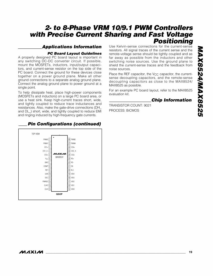
Pin Configurations (continued)
28
27
26
25
24
23
22
21
20
19
18
17
16
15
1
2
3
4
5
6
7
8
9
10
11
12
13
14
PWM2
PWM4
CS4+
CS2_4-
CS2+
RS+
VID0
RS-
EN
N.C.
VID4
VID3
VID2
VID1
CLKI
CLKO
PWRGD
OSC
ILIM
REF
COMP
GND
VCC
CS3+
CS1_3-
CS1+
PWM1
PWM3
QSOP
TOP VIEW
MAX8524
MA
X8
52
4/M
AX
85
25
2- to 8-Phase VRM 10/9.1 PWM Controllers with Precise Current Sharing and Fast VoltagePositioning
20 ______________________________________________________________________________________
V DD
= 6.
5V
VID4
PWM
1
PWM
3
RS+
PWM
2
PWM
4
KA31
7MR
U4
REF
EN
ILIM
COM
P
AGND
PWRG
D
VID0
VID1
VID2
VID3
D3
RS-
CLKI
CLKO
DLY
LX1
DH1
BST1
PV1
PWM
2
INPU
T10
V TO
13.
2V
C18
0.1μ
FR1
5OP
EN
V CC
R12
10Ω
PWM
1VI
D5
V CC
DL1
PG1
PG2
BST2
DH2
LX2
DL2
C110
μF 25V C3
10μF 25
V
C210
μF 25V C4
10μF 25
V
L10.
6μH
L20.
6μH
N1
N3
D1
C13
0.22
μF
R8 3.3Ω
C14
0.22
μF
R9 3.3Ω
LX1
DH1
BST1
PWM
2
PWM
1
DL1
PG1
PG2
BST2
DH2
LX2
DL2
D2
C15
0.22
μF
R10
3.3Ω
C16
0.22
μF
R11
3.3Ω
CS2+
CS1_
3-CS
1+CS
3+CS
2_4-
CS4+
CS4+
CS2+
CS2_
4-CS
3+CS
1+CS
1_3-
OSC
CS1+
CS3+
CS1_
3-
OUTP
UT0.
8375
V TO
1.6
V,80
A
L1–L
4: P
ANAS
ONIC
,N1
, N4,
N7,
N10
, N13
–N16
: IRF
7811
WN2
, N3,
N5,
N6,
N8,
N9,
N11
, N12
: IRF
7822
NOTE
: C30
-C45
SEL
ECTE
D FO
R VR
M 1
0 TR
ANSI
ENT
RESP
ONSE
SPE
CIFI
CATI
ONS
AT 1
.2V
OR H
IGHE
R OU
TPUT
.
C26
470p
F
C24
0.22
μF
C23
680p
F
C22
1μF
10V
C21
2.2μ
F16
V
C20
2.2μ
FC1
92.
2μF
REF
R23
200k
Ω
R18
50Ω
R20
100Ω
R19
50Ω
R21
100Ω
R22
348Ω
R28
6.81
kΩ
R16
100k
Ω
R13
10Ω 5%
R27
100k
Ω
R26
28.3
kΩR1
8OP
EN
J1–5
3OU
TEN
V OUT
J1–5
2V0
_SEN
+
C30–
C39
390μ
F/2V
SPCA
PS
J1–1
1V0
_SEN
-
7 2112 8 9
R29
6.81
kΩ
J1–1
0V C
C-PW
RGD
PV2
N2
N13
N4
N6N5
N14
C510
μF 25V C7
10μF 25
V
C610
μF 25V C8
10μF 25
V
L30.
6μH
R S1
1mΩ
R S2
1mΩ
R324
Ω R424
Ω
C11
33nF C1
233
nF
N7
L40.
6μH
CS2+
CS4+
N10
N12
N11
N16
DLY
PV1
C17
0.1μ
FR1
7OP
EN
V CC
R14
10Ω
PV2
C25
470p
F
C27
470p
F
V IN+
V IN+
V IN+
CS2_
4-
V DD
= 6.
5V
C28
3.3n
FC29
3.3n
F
R5 402Ω
R6 1.3k
Ω
J1–5
4J1
–6J1
–7J1
–56
J1–8
J1–5
5
J1–1
J1–2
J1–3
VO+
VO-
C40–
C45
470μ
F/6V
SPCA
PS
6
10
2 1 15 20 19 18 17 16 14 13 26 24 25 5 3 4 28 27
23 22 11
4 13 7 8 9 10121415166 113 521
4 13 7 8 9 10121415166 113 521
12
3
21
3
3 21
2
1
35 6
78
4
123
5 678
4
123
5 678
4
123
5 678
4
123
5 678
4
123
5 678
4
123
5 678
4
123
5 678
4
123
5 678
123
4 5 678
123
4
5 678
123
4
N15
5 678
123
4
N8
5 678
12
34 5 6
78
12
3
4
5 678
12
3
4
N9
5 678
12
34
J1–1
3J1
–15
J1–1
7J1
–19
J1–2
1J1
–23
J1–2
5J1
–27
J1–2
9J1
–31
J1–3
2J1
–34
J1–3
6J1
–38
J1–4
0J1
–42
J1–4
4J1
–46
J1–4
8
J1–1
4J1
–16
J1–1
8J1
–20
J1–2
2J1
–24
J1–2
6J1
–28
J1–3
0J1
–33
J1–3
5J1
–37
J1–3
9J1
–41
J1–4
3J1
–45
J1–4
7J1
–49
J1–5
0
R25
5.11
kΩR2
428
.7kΩ
R S1
1mΩ
R S2
1mΩ
R124
Ω R224
ΩC1
033
nFC9 33nF
MAX
8525
U1
MAX
8523
U2
MAX
8523
U3
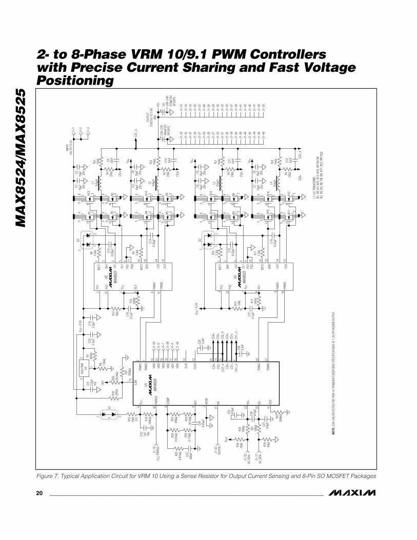
Figure 7. Typical Application Circuit for VRM 10 Using a Sense Resistor for Output Current Sensing and 8-Pin SO MOSFET Packages
MA
X8
52
4/M
AX
85
25
2- to 8-Phase VRM 10/9.1 PWM Controllers with Precise Current Sharing and Fast Voltage
Positioning
______________________________________________________________________________________ 21
V DD
= 6.
5V
VID4
PWM
1
PWM
3
RS+
PWM
2
PWM
4
KA31
7MR
U4
REF
EN
ILIM
COM
P
AGND
PWRG
D
VID0
VID1
VID2
VID3
D3
RS-
CLKI
CLKO
DLY
LX1
DH1
BST1
PV1
PWM
2
C18
0.1μ
F
V CC
R12
10Ω
PWM
1VI
D5
V CC
DL1
PG1
PG2
BST2
DH2
LX2
DL2
D1
C13
0.22
μF
R8 0Ω
C14
0.22
μF
R9 0Ω
LX1
DH1
BST1
PWM
2
PWM
1
DL1
PG1
PG2
BST2
DH2
LX2
DL2
D2
C15
0.22
μF
R10
0Ω
C16
0.22
μF
R11
0Ω
CS2+
CS1_
3-CS
1+CS
3+CS
2_4-
CS4+
CS4+
CS2+
CS2_
4-CS
3+CS
1+CS
1_3-
OSC
L1–L
4: T
DK, S
PM12
535T
-R23
M30
0N1
, N3,
N5,
N7:
IRF7
801
N2, N
4, N
6, N
8: 2
XIRF
7822
, EAC
H
C26
470p
F
C24
0.22
μF
C23
680p
F
C22
1μF
10V
C21
2.2μ
F16
V
C20
2.2μ
FC1
92.
2μF
REF
R23
95kΩ
R18
50Ω
R19
50Ω
R20
100Ω R2
110
0Ω
R22
29kΩ
R15
11.9
kΩ
R16
100k
Ω
R13
10Ω 5%
R27
27kΩ
R26
10kΩ
R18
OPEN
OUTE
N
V OUT
V0_S
EN+
V0_S
EN-
7 2112 8 9
R24
6.8k
ΩJ1–1
0V C
C-PW
RGD
PV2
DLY
PV1
C17
0.1μ
F
V CC
R14
10Ω
PV2
C25
470p
F
C27
470p
F
V DD
= 6.
5V
C28
0.01
5μFC2
90.
015μ
F
R5 249Ω
R6 1.02
kΩ
6
10
2 1 15 20 19 18 17 16 14 13 26 24 25 5 3 4 28 27
23 22 11
4 13 7 8 9 10121415166 113 521
4 13 7 8 9 10121415166 113 521
12
3
21
3
3 21
2
1
3
MAX
8525
U1
MAX
8523
U2
MAX
8523
U3
N1 N2R1
24Ω
C110
μF 25V
C210
μF 25V
L10.
29μH
C90.
033μ
F
R S1
1mΩ
VIN+
N3 N4R2
24Ω
C310
μF 25V
C410
μF 25V
L20.
29μH
C10
0.03
3μF
R S2
1mΩ
N5 N6R3
24Ω
C510
μF 25V
C610
μF 25V
L30.
29μH
C11
0.03
3μF
R S3
1mΩ
N7 N8R4
24Ω
C710
μF 25V
C810
μF 25V
L40.
29μH
C12
0.03
3μF
R S4
1mΩ
CS1+
CS3+
CS2+
CS4+
CS_4
-
C30–
C39
330μ
F/10
mΩ
SPCA
PS
VO+
VO-
CS1_
3-
V OUT
= 8
0A
V IN+
V IN+
V IN+
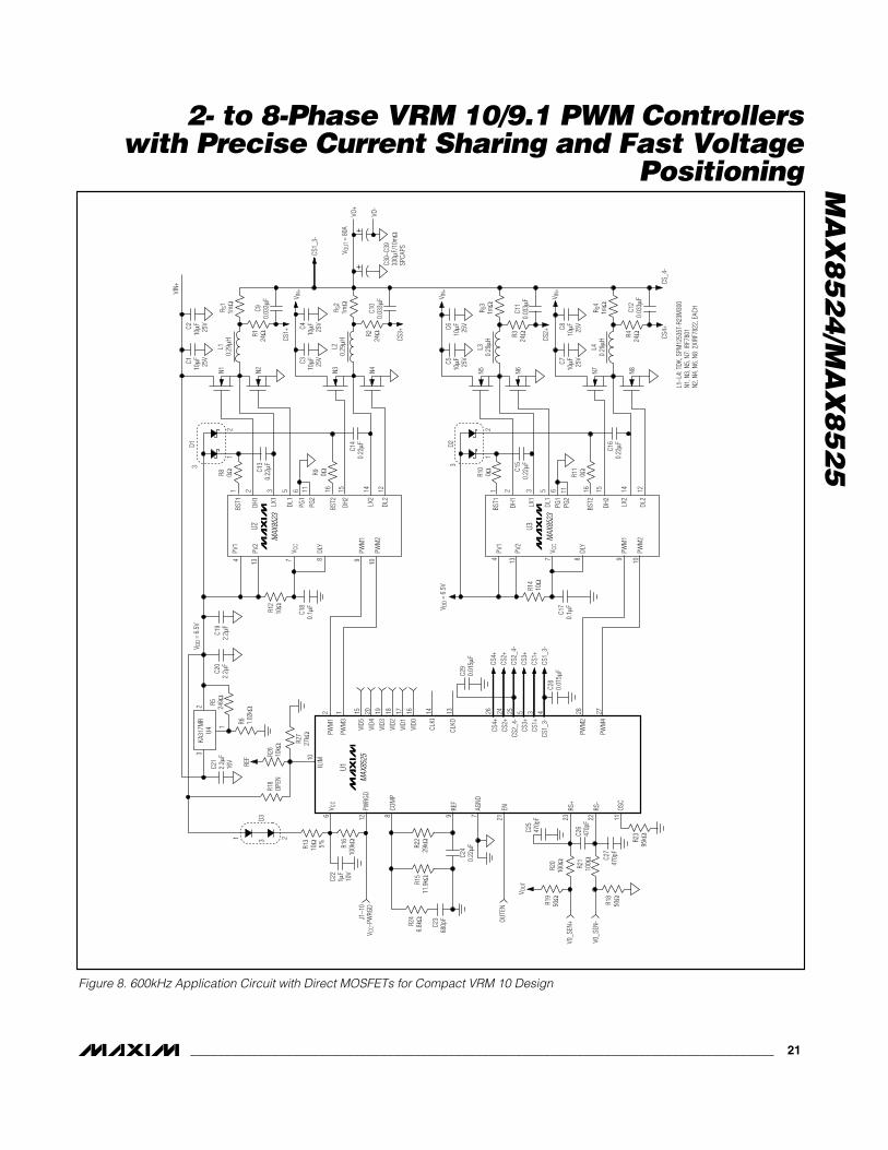
Figure 8. 600kHz Application Circuit with Direct MOSFETs for Compact VRM 10 Design
MA
X8
52
4/M
AX
85
25
2- to 8-Phase VRM 10/9.1 PWM Controllers with Precise Current Sharing and Fast VoltagePositioning
22 ______________________________________________________________________________________
7-BITCOUNTER
LOAD
VID1
VID2
VID4
VID3
PWM1
REF
DAC
INTERNAL CLOCK
COMP
CS1+
RS+
RS-
PWM2
PWM3
PWM4
CS3+
GND
CS2+
CS4+
EN
OPERATIONMODE DETECT
VID0
225mV
UVLO
OVP
0.9MHz TO 9.6MHz
OSCILLATOR
CURRENT FOLDBACKAND FAULT LOGICPWRGDPWRGD
VCC
OSC
CS2_4-
(MAX8525 ONLY) VID5
SYNCDETECTCLKI
CLKO
CS1_3-
ILIM
div 2
MUXdiv 2/3/4
S/R
S/R
S/R
S/R
0.45MHz TO 4.8MHz
1
0
RSDA
GMV
RCS
EQUA
L?
1μsDELAY
NO
REF
SOFT-START
RSNS1
RU
RBCC
REF2V ±0.4%
REFOKAND
100kΩ
RUN
ONE OF FOUR PHASES DEPICTED
OFFS
ET R
OM
RAPID-ACTIVE
AVERAGECURRENT
SENSE
GMCPHASE 1
GMCPHASE 2
GMCPHASE 3
GMCPHASE 4
BUF CLAMP
REF /2
PWM
PWM
PWM
PWM
S
S
S
S
MAX8524MAX8525
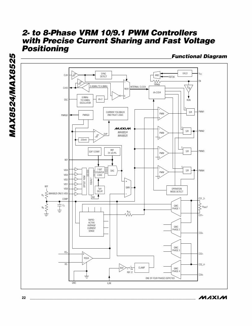
Functional Diagram
MA
X8
52
4/M
AX
85
25
2- to 8-Phase VRM 10/9.1 PWM Controllers with Precise Current Sharing and Fast Voltage
Positioning
Maxim cannot assume responsibility for use of any circuitry other than circuitry entirely embodied in a Maxim product. No circuit patent licenses areimplied. Maxim reserves the right to change the circuitry and specifications without notice at any time.
Maxim Integrated Products, 120 San Gabriel Drive, Sunnyvale, CA 94086 408-737-7600 ____________________ 23
© 2005 Maxim Integrated Products Printed USA is a registered trademark of Maxim Integrated Products, Inc.
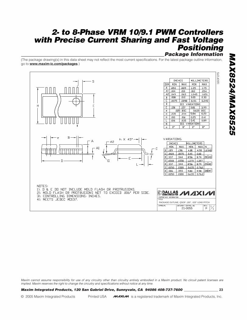
Package Information(The package drawing(s) in this data sheet may not reflect the most current specifications. For the latest package outline information,go to www.maxim-ic.com/packages.)
QS
OP
.EP
S
F1
121-0055
PACKAGE OUTLINE, QSOP .150", .025" LEAD PITCH