2020 edition - irds.ieee.org
TRANSCRIPT
THE INTERNATIONAL ROADMAP FOR DEVICES AND SYSTEMS: 2020 COPYRIGHT © 2020 IEEE. ALL RIGHTS RESERVED.
INTERNATIONAL ROADMAP
FOR DEVICES AND SYSTEMSTM
2020 EDITION
PACKAGING INTEGRATION
WHITE PAPER
THE IRDS IS DEVISED AND INTENDED FOR TECHNOLOGY ASSESSMENT ONLY AND IS WITHOUT REGARD TO ANY COMMERCIAL CONSIDERATIONS PERTAINING TO INDIVIDUAL PRODUCTS OR EQUIPMENT.

THE INTERNATIONAL ROADMAP FOR DEVICES AND SYSTEMS: 2020 COPYRIGHT © 2020 IEEE. ALL RIGHTS RESERVED.
© 2020 IEEE. Personal use of this material is permitted. Permission from IEEE must be obtained for all other uses, in any current or future media, including reprinting/republishing this material for advertising or promotional purposes, creating new collective works, for resale or redistribution to servers or lists, or reuse of any copyrighted component of this work in other works.
Bluetooth® SIG and its members, licensors, and suppliers own all right, title, and interest (including intellectual property rights) in the Services, Content, and all draft and adopted specifications for the Bluetooth standard and reserve all rights not expressly granted to you in these Terms or, if applicable, the SIG Member Terms. The Bluetooth logos and word marks referenced in the Services and Content are the trademarks of Bluetooth SIG and its affiliates. Any other company names, product names, service names and logos referenced in connection with the Services or Content may be the trademarks of their respective owners.
Wi-Fi® and Wi-Fi Alliance® are registered trademarks of Wi-Fi Alliance.
The IEEE emblem is a trademark owned by the IEEE.
"IEEE", the IEEE logo, and other IEEE logos and titles (IRDSTM, IEEE 802.11™, IEEE P1785™, IEEE P287™, IEEE P1770™, IEEE P149™, IEEE 1720™, etc.) are registered trademarks or service marks of The Institute of Electrical and Electronics Engineers, Incorporated. All other products, company names or other marks appearing on these sites are the trademarks of their respective owners. Nothing contained in these sites should be construed as granting, by implication, estoppel, or otherwise, any license or right to use any trademark displayed on these sites without prior written permission of IEEE or other trademark owners.

THE INTERNATIONAL ROADMAP FOR DEVICES AND SYSTEMS: 2020 COPYRIGHT © 2020 IEEE. ALL RIGHTS RESERVED.
Table of Contents Acknowledgments ................................................................................................................. v 1. Introduction and Mission Statement ................................................................................ 1
1.1. History ............................................................................................................................. 1 2. Overview of Roadmap Scope ......................................................................................... 3 3. Current Status ................................................................................................................. 4
3.1. Flip Chip ............................................................................................................................. 4 3.2. Comparison of Flip Chip and FO WLP ................................................................................. 6 3.3. Dealing with the High Cost of Fine Pitch Substrates and Mitigation .................................... 7 3.4. Coreless Organic Substrates (CL-OS) ................................................................................. 8 3.5. Hybrid Approaches ............................................................................................................... 8 3.6. 3D Stacks ............................................................................................................................. 9 3.7. Chiplets ........................................................................................................................... 11
4. Overall Advanced Packaging and Goals ....................................................................... 11 5. Summing up the Technical Challenges of Advanced Packaging .................................. 12
5.1. Non-Technical Terminology Problems of Advanced Packaging ........................................ 12 6. Summary—Simple Guidelines for the Future ................................................................ 13 7. Acronyms/Abbreviations ............................................................................................... 14 8. Appendices ................................................................................................................... 16
8.1. Appendix A—The Original Multi Chip Module (circa 1987) ................................................ 16 8.2. Appendix B—Substrate and I/O Density Roadmap (per Intel circa 2017) .......................... 17 8.3. Appendix C—Alternative 2D, 2.5D and 3D Package Configurations ................................. 18 8.4. Appendix D—Effect of Package Penalties on Power Loss and Bandwidth ........................ 19
THE INTERNATIONAL ROADMAP FOR DEVICES AND SYSTEMS: 2020 COPYRIGHT © 2020 IEEE. ALL RIGHTS RESERVED.
List of Figures Figure PI-1 Advanced packaging revenue is dominated by FC ............................................... 5 Figure PI-2 Typical FC implementation .................................................................................... 6 Figure PI-3 Schematic view of chiplets assembled via interposer and C4 bumps ................... 7 Figure PI-4 Hybrid approach using silicon bridge ..................................................................... 8 Figure PI-5 3D stack using combination of bumps, RDL and TSV for maximum density ......... 9 Figure PI-6 Breaking the memory wall by integrating HBM with 3D stacking ......................... 10 Figure PI-7 FC packaging technology allows a multitude of system solutions ....................... 11 Figure PI-8 IBM multi-chip module (circa 1987) with a 5 x 5 array of small chips C4
flip chip bonded to a glass-ceramic substrate...................................................... 16 Figure PI-9 Substrate and I/O density roadmap (per Intel circa 2017) ................................... 17 Figure PI-10 Planar DIMM ........................................................................................................ 18 Figure PI-11 PoP ...................................................................................................................... 18 Figure PI-12 2.5D Planar on fine-pitch Si substrate (as used for FPGAs from immature fab
process) ............................................................................................................... 18 Figure PI-13 CPU and separate 3D stack of DRAM (as used for a growing number of high
performance modules for game systems, servers, AI engines, etc.) ................... 18 Figure PI-14 Some oscillations at both logic “high” and “low” levels but still usable for digital
operation .............................................................................................................. 20 Figure PI-15 The use of TSVs produces very sharp and clean output waveform at 200 MHz . 20 Figure PI-16 I/O power reduction by TSV ................................................................................ 21
List of Tables Table PI-1 3D Package Performance.................................................................................. 22

THE INTERNATIONAL ROADMAP FOR DEVICES AND SYSTEMS: 2020 COPYRIGHT © 2020 IEEE. ALL RIGHTS RESERVED.
ACKNOWLEDGMENTS Dr. Dev Gupta (APSTL
Prof. Paul Franzon (ECE, UNC Rayleigh)
Plus industry representatives from an advance packaging technology developer and licensor, organic dielectric supplier, OSAT, and teardown and analyses service


Introduction and Mission Statement 1
THE INTERNATIONAL ROADMAP FOR DEVICES AND SYSTEMS: 2020 COPYRIGHT © 2020 IEEE. ALL RIGHTS RESERVED.
PACKAGING INTEGRATION WHITE PAPER 1. INTRODUCTION AND MISSION STATEMENT Packaging Integration (PI) refers to the integration of separately manufactured components into a higher-level assembly that in the aggregate provides enhanced functionality and improved operating characteristics.
In this definition components should be taken to mean any unit whether individual die (both logic, memory, application-specific integrated circuit (ASIC). etc.) and also micro electro mechanical system (MEMS) device, passive components and assembled package or sub-system that are integrated and encased into a single package. PI will also highlight combination of packages jointly assembled to further enhance system performance. Operating characteristics should also be taken in its broadest meaning including electrical, mechanical and also such system level considerations as cost of ownership.
Compared to the recently coined term of “heterogeneous integration”, PI or “dense off chip integration” (DOCI) are technically more accurate terms in describing the approach and strategy of using advanced packaging (AP) consisting of shrinks, higher feature densities of traditional package elements, materials and structures leading to tighter integration and better performance to integrate at the package rather than single chip level, systems that cost much less yet perform almost as well.
The overall approach of PI consists in identifying the requirements of integration of diverse components in the electronics industry through 2034; determine the difficult challenges that must be overcome to meet these requirements and identify potential solutions.
It is not the goal of PI to generate an historical and anthological compilation of different packaging solutions but the PI chapter concentrates on the efforts to optimally intermingle ICs of different kinds, other active and passive components and a multiplicity of so called packaging solutions to symbiotically enable optimal heterogeneous system integration.
The mission of the Packaging Integration Focus Team is to provide guidance to industry, academia and government organizations to identify key technical challenges with sufficient lead-time so that unaddressed challenges do not later on become roadblocks preventing the continuous progress of the electronics industry; to elucidate also basic principles behind Packaging Integration for new potential users so that they can better understand and analyze competing claims made by various providers. This guidance is essential to the future growth of society and its continued beneficial impact on mankind.
The upcoming IRDS Packaging Integration Roadmap addresses the need of:
(a) New and current users of advanced packaging who need to unravel the confusing terminology and conflicting messages presently dominating the packaging and assembly world and help users to make efficient choices not just aimed at the immediate future but also guide them towards cost-effective solutions in the long run.
(b) Motivating the electronic packaging industry (and also foundries that are recently joining in) to work on their future needs
(c) The electronic packaging industry itself to better understand Packaging Integration needs and further develop the more promising technologies capable of supporting a strong future business rather than getting overly distracted by short-term, stop-gap opportunistic solutions
(d) Informing the suppliers of design tools, materials, process and metrology equipment by providing a balanced short and long term visions of the “Big Picture” of the electronics industry and the pivotal role of PI; provide useful guidance for their own R&D programs.
1.1. HISTORY The term “electronic packaging” (EP) was coined after its original 1950s introduction at the dawn of the semiconductor age, that is, physically protecting the single fragile semiconductor transistors from the harsh external environment. Subsequently packaging evolved with the decades from encapsulating a single transistor to enclosing and protecting integrated circuits (ICs) with multi-billion transistors on a chip and also extending to multiple chips placed in a single enclosure. In recent years, the role of EP has substantially changed as its potential impact on system performance (e.g.,
2 Introduction and Mission Statement
THE INTERNATIONAL ROADMAP FOR DEVICES AND SYSTEMS: 2020 COPYRIGHT © 2020 IEEE. ALL RIGHTS RESERVED.
breaking the “Memory Wall”) has been recognized even though the generic packaging terminology (EP) continues to be applied.
However, since many additional functions are now included under the electronic packaging terminology it is necessary to address all of them. These are as follows:
i. Providing protection for one or multiple ICs from the outside environment
ii. Providing numerous interconnects that allow complex ICs to communicate with the outside world (e.g., boards, electronics racks and systems)
iii. Removing the heat generated during IC operations
iv. Integrating individual ICs that may be fabricated with incompatible technologies (e.g., Si processor and DRAM chips, Si logic and GaAs power amplifiers (PAs), etc.) to create a module or even the whole system
Until a decade ago most advanced packaging technologies had been developed by well-established independent device manufacturers (IDMs) and by some Japanese system companies; all of them had large R&D budgets that allowed them to invest into a field (i.e., packaging) where economic margins have historically been very small. In few words, the traditional packaging and assembly companies could not afford these investments that however were essential to maintain a healthy growth of the electronics industry. In the past new technologies gradually seeped from IDMs and system companies into the contract packaging industry known as the out-sourced assembly and test (OSATs). As time went by, these contractors began also supporting the Fabless design companies; especially those located in Silicon Valley who were quick to adopt this new “ design only” business strategy.
Around 2010 CMOS foundries that were very close to the leading edge of IC technology began taking on more and more aggressive programs, accepting business just beyond their capabilities at the time. When confronted with low yields for very large die (e.g., field-programmable gate arrays (FPGAs)) produced at a new and immature node (around the so called 28 nm technology generation) they decided to minimize their shortcomings by resorting to packaging technologies to at least partially overcome this problem. The most prudent approach consisted in adopting a well-proven packaging technology first introduced by IBM over 30 years earlier (see Appendix A). This well-established playbook called for multi-chip packaging to succeed where IC yields of large die could not. At the original introduction time this multi-chip module (MCM) technology had been demonstrated by depositing an array of solder bumps (high melting point around 330°C) typically located on top of bonding pads uniformly spaced 300 microns apart around the edge of the die. To attach the chip into a board, the chip was then flipped (i.e., flip chip (FC)) to bring the solder dots in contact with line connectors pre-defined on the underlying circuit board. Finally, the solder bumps were then partially melted to produce an electrical connection, typically melting the solder. This last process step provided very reliable and numerous connections between the IC and the undelaying board connectors.
This process was well known under the name of “Control Collapse Chip Connection”, abbreviated as C4. A later lower cost electroplated version first introduced by Motorola Semiconductor in 1991, which became the industry standard for processors, was successfully marketed by several assembly houses for FCs on Si substrates. In few words, this rediscovered solution consisted in partitioning any large single die like an FPGA into several smaller chips (“chiplets”) and then after test re-integrating the original functionality by assembling only the known good dies (KGDs) or “chiplets” and connecting them with MicroPillar flip chip technology that uses metal pillar type bumps at a tight 50 micron pitch invented at Motorola Semiconductor and first used for GaAs power amplifiers some 15 years earlier. This time however, as silicon substrate technology had further progressed, a standard dual Damascene process in common use in the back end of line (BEOL) of fabs and best foundries was successfully introduced to fabricate the silicon substrate. These interconnect lines were laid out with a much higher density at a 2 micron pitch. At the end of all these process steps, the overall yields of the individual smaller die assembled by the thermocompression flip chip bonding process (originally developed for GaAs power amplifiers) were much higher as compared to the yields of any single large chip fabricated with the limited level of maturity of IC processes available at the time.
This module approach was successfully introduced with actual FPGA products yielding very viable commercial products and it established the leadership position of the company that aggressively pursued this technological hybrid solution. This tangible economic success brought advanced packaging to the attention of fabless design companies, which up to this time had been oblivious to this aspect of semiconductor technology and were barely beginning to take advantage of existing packaging technologies developed by IDMs and later on made available to them via OSATs. However, the foundries that demonstrated that technology were now in the position of offering even more integrated IC/packaging solutions. Several of the fabless design companies developed new high-performance modules taking advantage of a

Overview of Roadmap Scope 3
THE INTERNATIONAL ROADMAP FOR DEVICES AND SYSTEMS: 2020 COPYRIGHT © 2020 IEEE. ALL RIGHTS RESERVED.
variety of FC and packaging integrated solutions; seeing the obvious commercial benefits several of the fabless design companies began to adopt expensive Si substrate/interposer technology services offered to them by the foundries.
To compete with the new foundry-provided Packaging Integration solutions, the OSATs accelerated their in-house development of similar but cheaper technologies (e.g., less expensive substrates and not quite as fine interconnect pitch as produced with dual Damascene or altogether substrate-less wafer-level chip-scale packaging using expensive fab tools). However, IDMs still maintained their technical PI leadership (as demonstrated by their ability of developing better integrated solutions very well-tailored to their needs) by producing customized solutions; by controlling and balancing IC and packaging solutions (since they possessed both expertise as well as the freedom of designing chips) to take advantage of any trade-offs between both IC and PI technologies. This level of flexibility enabled these IDMs to exploit the most cost-effective overall solutions (See below for details of optimized technologies like embedded multi-die interconnect bridge (EMIB) that only IDMs could develop).
However, a multitude of combinations of IC designs and packaging integration solutions have emerged outside the IDM environment in recent times. Many of these combinations are viable but are not necessarily well balanced between IC and package partitioning producing overall sub-optimal integration. As a result, an explosion of confusing and questionable claims has emerged. In many cases with the outcome not quite as cost effective as many believe. In addition, information and recommendations provided with simplistic technical expertise have created additional confusion and have produced questionable forecasts.
It is absolutely necessary for the PI Roadmap to clarify these issues and guide future developments for maximum benefit to all concerned.
2. OVERVIEW OF ROADMAP SCOPE a. Recent Impacts of Advanced Packaging & Packaging Integration—Flip chip parallelism, 2.5D tight integration, and TSVs in 3D stack high-bandwidth memory (HBM). All together, these packaging technologies have allowed breaking the “Memory Wall” by doubling data transfer throughput and halving energy requirements like it has been demonstrated by Google tensor processing unit (TPU) before and after enabling use of HBM
b. New Technology Drivers—New applications (e.g., antenna in package) need to fit within new system boundaries, performance, cost reduction
c. Fundamental Technical Goals—Minimize packaging penalties (arising out of losses, delays and noise while transmitting signals across packages) by developing new technologies. Whenever the electrical signals leave the IC and propagate within a package via interconnections it is in general impossible to eliminate adverse effects introduced by parasitics like capacitance of long lines and inductance of long vias. These parasitics’ effects increase signal rise/settling time and increase the amount of energy required to transmit data. It is a goal of PI to reduce signal and energy losses by proposing ways of reducing both parasitics and lower the clock rate (to reduce the energy required to transmit data) while signal rates increase. This is accomplished by widening the data bus and by reducing parasitics.
Other items to keep under consideration to minimize packaging penalties are:
• Shrinking geometries (smaller lines have higher resistance)
• Shrinkage of geometries and interleaving of multiple layers with incompatible thermo mechanical properties causes residual stress and warpage that may induce fatigue in weak links, leading to reliability problems
d. Current Advanced Packaging—Flip chip (bumps, substrates, assembly, underfill), fan-out wafer-level package (FO WLP), through silicon vias (TSVs)
e. Dense Planar Integration—2.5D, EMIB, FOVEROS
f. 3D Stacked Die Integration—Package on package (PoP) (used widely in smart phones to stack and peripherally interconnect the system on chip (SoC) and DRAM), hybrid memory cube (HMC) (now defunct due to the unfortunate choice of a very fast serializer/deserializer (SERDES) serial connection over a slower, low-loss parallel bus between the memory stack and central processing unit (CPU)), HBM (used to stack 8 or more DRAM die and interconnect them through a central core of an array of TSVs to wide and slow parallel bus), heat removal from stacked “chiplets” that run hot (e.g., processors)

4 Current Status
THE INTERNATIONAL ROADMAP FOR DEVICES AND SYSTEMS: 2020 COPYRIGHT © 2020 IEEE. ALL RIGHTS RESERVED.
g. Technologies in Development—Finer pitch organic substrates (SWIFT, embedded line, integrated thin-film high-density organic package (ITHOP, etc.), FO WLP and fan-out panel-level package (FO PLP), comparison w/coreless FC, TSV shrink, faster thermocompression bonding (TCB), alternatives like direct bond interconnect (DBI)
h. Issues of FO WLP and FO PLP and mitigation—Cost increase of FO WLP over incumbent flip-chip packaging as the fan out ratio increases, die shift, wafer and panel warpage, the need for new mold materials
3. CURRENT STATUS 3.1. FLIP CHIP For the past 30 years the workhorse for advanced packaging technology has been various versions of flip chip (FC) on organic substrates.
Flip-chip technology is now a $ 24 billion a year market, as part of the $ 400 billion a year Semiconductor industry
Flip chip is essentially a vertical and area-array interconnect system using various fusible metallurgies (called bumps) deposited on the bond pads of ICs when they are still at the wafer level during what is called the back end of line (BEOL) processing. Separated and tested good chips with the bumps are flipped over a high-density circuit board (called a substrate). The bumps on the chip are then aligned to corresponding bond pads on the substrate using high-precision/high-speed robots with machine vision. The metallurgies of the carefully aligned bond pad-interconnect are then fused (reflowed in a reducing atmosphere) and alloyed to form an area array of robust joints.
FC technology has replaced the previous generation of packaging interconnects constituted of wire bonded (WB) to the IC bond pads and to the package landing pads, which in turn were connected to the package outside pins. It should be noted that die and package wire connections required bond pads to be located at the edge of the die and landing pads surrounding them inside the package. This arrangement limited the number of interconnects from any die to the outside world via the package pins by requiring them to be located at the periphery of the die. FC multiplies the number of interconnects per chip by allowing any location within the area of the die to be connected to the outside world typically substantially increasing the number of die outputs. This packaging-driven arrangement allowed implementation of a higher level of signal parallelism (e.g., multi processors both CPUs and graphic processing units (GPUs)) on a single chip and corresponding reduced power dissipation. Also inductance due to package interconnects was reduced by an order of magnitude with FC over WB due to drastic reduction of interconnects’ lengths with consequent improvement in power and signal integrity.
Several advancements in FC technologies have also contributed to making this approach more viable and cost effective than in the past. Earlier versions of flip-chip technology had been developed in the 1960s and used to build multi-chip modules for mainframes. At that time proven but rather conservative and expensive physical vapor deposition (PVD) (i.e., sequential evaporation of Pb and Sn through a Mo metal mask onto the wafers) methods had been used to deposit the vertical interconnects (the bumps) on the whole wafer. However, since the early 1990s much cheaper chemical deposition (e.g., electrodepositing with associated photoresist patterning and etching) have been used. At first this deposition technology was deemed rather risky due to chances of contaminating the bondable metallization with the chemicals used during deposition but development of both new chemistries and tools solved the problem. By 1992 it went into volume production for bipolar ASICs for supercomputers. In addition, to reduce thermal mismatch-induced stresses demanding the use of only materials thermally compatible with silicon (e.g., alumina-silicate ceramics) imposed some limitations on wiring density. Furthermore, the assembly process then practiced involved manual alignment with fixtures and it was still practiced in this way even into the late 1980s.
The now industry standard electroplated flip-chip technology was originally developed in the early 1990s using rigorous theoretical methods (ranging from metallurgy, electrochemistry, polymer chemistry to fluid mechanics, heat transfer, stress analysis, circuit simulation, mathematical modeling and simulation, etc.) to make FC compatible with the electrical requirements and cost structure of microprocessors. This flip-chip technology uses electroplated bumps and organic substrates, high-precision (+/- 5 um) assembly robots using machine vision capable of 1,000 units per hour that were developed to replace slow manual alignment and assembly. This new and improved flip-chip technology reduced cost by some 5x over the incumbent. For the last quarter century it has been in high-volume manufacturing (HVM) at major IDMs for both CMOS Si as well as GaAs and, due to its robustness and affordability, has become the industry standard for high-I/O density, high-performance applications.
FC now has very broad applications ranging from original microprocessors as well as the latest SoCs, low cost GaAs power amplifiers (which enable fast data transfer by RF thus Internet and video access from handhelds) to newer

Current Status 5
THE INTERNATIONAL ROADMAP FOR DEVICES AND SYSTEMS: 2020 COPYRIGHT © 2020 IEEE. ALL RIGHTS RESERVED.
applications such as back-illuminated sensors (BIS) imaging chips, flat panel displays, lasers, light-emitting diodes (LEDs), and 3D stacked chips, including logic chip and HBM memories.
Flip chip is mandatory for package-level integration of chips that demand dense off chip integration (DOCI) to minimize package penalty on performance.
Over the last 3 decades the electroplated flip chip market has grown from beaker experiments to fully robotic wafer bumping and assembly lines. It is now a $ 24 billion a year industry worldwide business (approximately 5% of the semiconductor industry) (Figure PI-1).
Figure PI-1 Advanced packaging revenue is dominated by FC In 2020 FC makes up $24 billion or 73 % out of a total of $33 billion for all types of advanced packaging. Advanced packaging itself is 80 % of total packaging. (Figure PI-1). (All packaging is about 10 % of the total semiconductor industry.)
Over the last decade FC technology (Figure PI-2) has become very popular and diffused to offshore manufacturers concentrated mostly in Taiwan and South Korea that support much of the fabless design companies.
It should be noted that the fine-pitch organic substrates needed for flip chip can at times cost as much as the die itself. This is very expensive for many contract assemblers and testers (OSATs). As a result, the larger providers of the FC technology assembly, already experienced in BEOL processing to do wafer bumping for flip chip, are now busy developing substrate technologies or packaging schemes that DO NOT require a substrate at all (e.g., FO WLP and FO PLP). These FP FC suppliers are now building all the technologies required including substrates. In these new technologies the wafer is diced first. But then the die are very precisely re-positioned on a carrier wafer or panel, with space kept around each die. The carrier is then reconstituted by molding followed by making a redistribution layer atop the entire molded area (both atop the chip and atop the adjacent fan-out area), and then forming solder-balls on top.

6 Current Status
THE INTERNATIONAL ROADMAP FOR DEVICES AND SYSTEMS: 2020 COPYRIGHT © 2020 IEEE. ALL RIGHTS RESERVED.
Figure PI-2 Typical FC implementation
3.2. COMPARISON OF FLIP CHIP AND FO WLP Proponents of the emerging FO WLP technology claim that it has better electrical performance compared to flip chip. However that is true only if the comparison is made with flip chip on substrate with a stiffener core (the volumetrically dominant version, in which the up to 150 micron long through vias in the core add to the inductance loop considerably ) but NOT so if it is with flip chip on a coreless substrate. Similar arguments apply for the thickness of assembled packages.
The finer geometries possible with FO WLP (down to 2 micron L/S claimed) compared to dominant approaches to fabricate substrates for flip chip (with stiffener cores, in large panels processed using projection aligners, etc.) are certainly credible because WLPs are made on wafers (original Si for WLPs or composite reconstituted for FO WLPs) in the fab using fab tools (steppers, etc.). These differences however disappear for at least two processes for coreless substrates for FC as they too are made in the fab.
Flip chip on substrates require wafer bumping, a separate substrate from a supplier, then assembly of the two. FO WLPs do not require wafer bumping or assembly and the substrate is built up in the fab itself on a reconstituted wafer. So at least superficially it is only natural to expect that packaging cost for FO WLPs would be lower than for flip chip.
However this is not necessarily true for all cases and depends on the fan-out ratio (the ratio between the area of the package and the die size contained in it) and depends on the I/O count and density limits imposed by the next lower level of the overall packaging-assembling scheme (e.g., the motherboard). Typically if the fan out ratio exceeds 2, then the cost of FO WLP approaches that of FC and, at higher ratios, may even exceed it. This is because as the fan out ratio increases fewer chips can be accommodated in a single reconstituted wafer. Having to process more wafers to package the same number of chips increases the cost of FO WLP package. Flip chip does not suffer from this issue as no reconstituted wafer is needed and the fan out interconnects are all contained in a single substrate processed as a large panel before it is separated in individual elements.
It can be seen from these considerations that a fair comparison of the overall cost reduction by switching from flip chip to FO WLP is strongly affected by the initial assumptions. If however, the same supplier does both the IC and the FO WLP it is not possible to separate the process yields or packaging cost. So even though this solution may be advantageous in some special cases (e.g., small packages for automotive radars with a limited no. of I/Os or large MCMs for servers requiring fine line interconnects between the chips but a low fan out ratio) it may not represent an industry wide trend as

Current Status 7
THE INTERNATIONAL ROADMAP FOR DEVICES AND SYSTEMS: 2020 COPYRIGHT © 2020 IEEE. ALL RIGHTS RESERVED.
demonstrated by the fact that only one out of 3 or 4 major designers/manufacturers in the very competitive area of SoCs for smart phones and tablets have decided to switch from FC to WLPs (offered by their foundry).
The low area utilization of round 300 mm reconstituted wafers used to process FO WLPs for large die (say 12 mm sq. or larger) and fan out ratios >2 (as is frequently the case for processor chips) has spurred development efforts in fan out panel level packaging (FO PLP). Panels up to 600 mm square are contemplated for this technology. To shrink the current best L/S of panel processing (flip-chip substrates with L/S of 8 micron) to below 5 um, panel lithography for FO PLP will need to replace projection aligners with steppers and high-throughput process tools for coating, deposition, etching, etc., with better uniformity due to switching from symmetric 300 mm wafers to larger square panels.
There are other limits in FO WLP and FO PLP schemes not obvious at first glance. Typical FO WLP process flow requires separated die to be placed and loosely attached to an adhesive-coated back-up carrier, then it is molded to lock in the die to create the reconstituted wafer (on which the interconnect metallization is patterned and deposited). But there may be some die shift and reconstituted wafer/panel warpage during the thermoset molding process limiting the lithography resolution.
To limit panel distortion with effects on both lithography as well as residual stress, a very large overseas IDM has adopted the interim strategy of cutting pockets in large panels, filling them in with soft polymers then embedding die into them to create a hybrid reconstituted panel before building up the interconnect layers on the whole panel. This scheme is used to build MCMs/SiPs for watches.
For the FO PLP effort to succeed, what is urgently needed is the development of new molding compounds that will limit warpage and stress even in large reconstituted panels.
3.3. DEALING WITH THE HIGH COST OF FINE PITCH SUBSTRATES AND MITIGATION Around 2010 foundries were eager to begin shipping wafers at their leading-edge nodes even before the technology had reached full maturity (i.e., high yields). This task was particularly challenging for products like FPGAs due to the typically large die size but in the environment at that time they realized that advanced packaging (with a profit margin 2x of conventional packaging) was a real opportunity and decided to take advantage of this opportunity and revived a 30+ year-old IBM technology of MCM. This revived technology was marketed under the new name of “2.5D interposer” (Figure PI-3). This technology was very successful. In summary, MCM was reinserted just at the right time to mitigate process immaturity at offshore foundries.
Figure PI-3 Schematic view of chiplets assembled via interposer and C4 bumps
However, while the technology gap was temporarily closed by means of this reborn MCM approach it became necessary to address the cost problem. Silicon substrates made at the foundry by the dual Damascene process with interconnect geometries going down to sub-micron dimensions certainly met the interconnect density needs of even fragmented FPGAs but cost orders of magnitude more than basic standard organic substrates with interconnect geometries limited to no finer than the 10 micron possible on large panels using cheaper lithography and processing tools. Furthermore, the need for long TSVs in thick Si interposers (at least 150-microns thick to ensure good mechanical stability) added more

8 Current Status
THE INTERNATIONAL ROADMAP FOR DEVICES AND SYSTEMS: 2020 COPYRIGHT © 2020 IEEE. ALL RIGHTS RESERVED.
cost and as well as unwanted inductance affecting electrical performance. These considerations explain why the silicon interposer technology is not cost effective for low-cost high-volume consumers’ applications.
3.4. CORELESS ORGANIC SUBSTRATES (CL-OS) CL-OS have been around for 20 years and were developed to reduce problems due to long through vias that degrade electrical performance (high inductance) in baseline substrates with a stiffener core. When the dielectric and redistribution (conductor) of CL-OS are built up over flat glass wafers (300 mm) or larger panels, the improved planarity enables fine L/S down to 2 microns. Chips with Sn capped micro-pillar bumps (as for 2.5D Si interposers) are directly thermocompression-FC bonded to the substrate over glass carriers, then over molded for stiffness, de-bonded from the carrier by one of several processes (e.g., laser de-bonding). Ball grid array (BGA) solder balls are attached and then the wafer/panel is tested and the individual devices are separated. However, foundries naturally favor more use of their Silicon interposers and given the strong relation/interdependence of fabless companies and foundries, so far coreless substrates (CL-OS ) for cost-effective DOCI is mostly used by IDMs.1
3.5. HYBRID APPROACHES There are however other solutions to this problem. IDM companies as stated before have more flexibility since they can optimize the overall product by appropriately partitioning functionalities between the IC and package. A viable alternative consists in making full use of existing advanced packaging technologies (including in situ flip chip bonding first developed and used a quarter century ago for GaAs PAs in mobile phones) by taking a hybrid approach.
The EMIB approach developed at a leading IDM (Figure PI-4) embeds a small piece of silicon substrate with high interconnect density (L/S < 2 microns) into a normal density (L/S > 10 microns) organic substrate but ONLY where it is needed (i.e., the peripheral areas of large die where the I/O density is higher); coarser interconnect lines in the central part of the die suffice for power delivery. By so doing the area of expensive Si substrate is reduced by a significant factor (2 or 3). However this approach requires more advanced flip-chip bumping and bonding techniques not well known outside the IDM community.
Figure PI-4 Hybrid approach using silicon bridge
1 https://ieeexplore.ieee.org/document/8811109
Current Status 9
THE INTERNATIONAL ROADMAP FOR DEVICES AND SYSTEMS: 2020 COPYRIGHT © 2020 IEEE. ALL RIGHTS RESERVED.
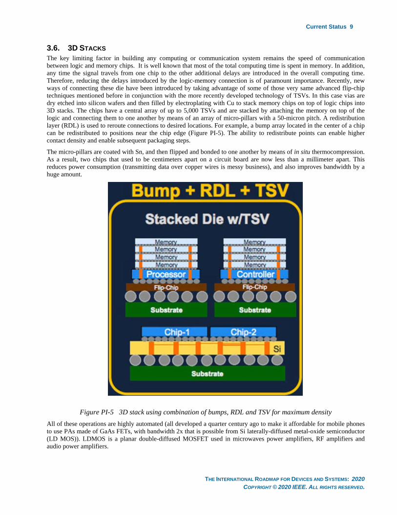
3.6. 3D STACKS The key limiting factor in building any computing or communication system remains the speed of communication between logic and memory chips. It is well known that most of the total computing time is spent in memory. In addition, any time the signal travels from one chip to the other additional delays are introduced in the overall computing time. Therefore, reducing the delays introduced by the logic-memory connection is of paramount importance. Recently, new ways of connecting these die have been introduced by taking advantage of some of those very same advanced flip-chip techniques mentioned before in conjunction with the more recently developed technology of TSVs. In this case vias are dry etched into silicon wafers and then filled by electroplating with Cu to stack memory chips on top of logic chips into 3D stacks. The chips have a central array of up to 5,000 TSVs and are stacked by attaching the memory on top of the logic and connecting them to one another by means of an array of micro-pillars with a 50-micron pitch. A redistribution layer (RDL) is used to reroute connections to desired locations. For example, a bump array located in the center of a chip can be redistributed to positions near the chip edge (Figure PI-5). The ability to redistribute points can enable higher contact density and enable subsequent packaging steps.
The micro-pillars are coated with Sn, and then flipped and bonded to one another by means of in situ thermocompression. As a result, two chips that used to be centimeters apart on a circuit board are now less than a millimeter apart. This reduces power consumption (transmitting data over copper wires is messy business), and also improves bandwidth by a huge amount.
Figure PI-5 3D stack using combination of bumps, RDL and TSV for maximum density All of these operations are highly automated (all developed a quarter century ago to make it affordable for mobile phones to use PAs made of GaAs FETs, with bandwidth 2x that is possible from Si laterally-diffused metal-oxide semiconductor (LD MOS)). LDMOS is a planar double-diffused MOSFET used in microwaves power amplifiers, RF amplifiers and audio power amplifiers.
10 Current Status
THE INTERNATIONAL ROADMAP FOR DEVICES AND SYSTEMS: 2020 COPYRIGHT © 2020 IEEE. ALL RIGHTS RESERVED.
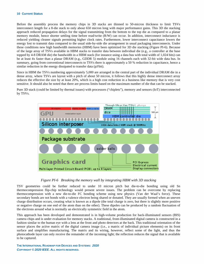
Before the assembly process the memory chips in 3D stacks are thinned to 50-micron thickness to limit TSVs interconnect length for a 8-die stack to only about 650 micron long with major performance gains. This 3D die stacking approach reduced propagation delays for the signal transmitting from the bottom to the top die as compared to a planar memory module, hence shorter settling time before read/write (R/W) can occur. In addition, interconnect inductance is reduced yielding cleaner signals permitting higher clock rates. Furthermore, lower interconnect capacitance lowers the energy lost to transmit data compared to the usual side-by-side die arrangement in usual packaging interconnects. Under these conditions new high bandwidth memories (HBM) have been optimized for 3D die stacking (Figure PI-6). Because of the large array of TSVs available in HBM stacks to transfer data between individual die (e.g., a controller at the base topped by 4-8 DRAM die) the bandwidth in a HBM stack (for instance using a data bus with total width of 1,024 bits) can be at least 4x faster than a planar DRAM (e.g., GDDR 5) module using 16 channels each with 32-bit wide data bus. In summary, going from conventional interconnects to TSVs there is approximately a 50 % reduction in capacitance, hence a similar reduction in the energy dissipated to transfer data (pJ/bit).
Since in HBM the TSVs numbering approximately 5,000 are arranged in the central part of the individual DRAM die in a dense array, where TSVs are layout with a pitch of about 50 micron, it follows that this highly dense interconnect array reduces the effective die size by at least 20%, which is a high cost reduction in a business like memory that is very cost sensitive. It should also be noted that there are process limits based on the maximum number of die that can be stacked.
Pure 3D stack (could be limited by thermal issues) with processors (“chiplets”), memory and sensors (IoT) interconnected by TSVs.
Figure PI-6 Breaking the memory wall by integrating HBM with 3D stacking TSV geometries could be further reduced to under 10 micron pitch but die-to-die bonding using old Sn thermocompression flip-chip technology would present severe issues. The problem can be overcome by replacing thermocompression with a new die-to-die FC bonding scheme using new physics (Van der Waal’s force). These secondary bonds are not bonds with a valence electron being shared or donated. They are usually formed when an uneven charge distribution occurs, creating what is known as a dipole (the total charge is zero, but there is slightly more positive or negative charge on one end of the atom than on the other). These dipoles can be produced by a random fluctuation of the electrons around what is normally an electrically symmetric field in the atom.
This approach has been developed and demonstrated is in high-volume production for back-illuminated sensors (BIS) camera chips and is under evaluation for memory stacks. A traditional, front-illuminated digital camera is constructed in a fashion similar to the human eye with a lens at the front and photo detectors at the back. This traditional orientation of the sensor places the active matrix of the digital camera image (i.e., a matrix of individual picture elements) on its front surface and simplifies manufacturing. The matrix and its wiring, however, reflect some of the light, and thus the photocathode layer can only receive the remainder of the incoming light; the reflection reduces the signal that is available to be captured.

Overall Advanced Packaging and Goals 11
THE INTERNATIONAL ROADMAP FOR DEVICES AND SYSTEMS: 2020 COPYRIGHT © 2020 IEEE. ALL RIGHTS RESERVED.
A BIS contains the same elements, but arranges the wiring behind the photocathode layer by flipping the silicon wafer during manufacturing and then thinning its reverse side so that light can strike the photocathode layer without passing through the wiring layer.
3.7. CHIPLETS Over the last 15 years, and spurred by competition, SoCs have grown to including multi processors in the same package as opposed to multicores in a single die (Figure PI-7). This approach is an evolution of multichip packaging originally developed for FPGAs (see Section 3.3). Once again, foundries have been offering this technology to their customers with excellent results. This concept is not different from what leading IDMs have done through the years, going back to the first dual-core implementations. It has always been felt that packaging technology is the best vehicle to bridge between two successive generations of fab technology by providing some capabilities before the single die integration has reached adequate yield levels. The latest variation of that is the recent “chiplet trend”, which is merely the latest terminology for the decades old MCM technology. To improve fab yields functional blocks in a processor or SoC are partitioned off to chiplets and then, as mentioned before, integrated at the package level by flip chip bonding them on to high-density substrates represented by inserting high-density interconnections by means of a silicon bridge or even a glass substrate.
Figure PI-7 FC packaging technology allows a multitude of system solutions
4. OVERALL ADVANCED PACKAGING AND GOALS Advanced packaging has always worked in conjunction with IC technologies. Severe electrical penalties are encountered anytime an electric signal leaves any pin of a packaged IC to travel to another packaged IC. As performance requirements have kept on increasing through the years it becomes necessary to develop more efficient packaging technologies eventually accommodating multiple chips within a single package cavity. For instance, early on packaging houses used traditional low-cost wire-bonding technologies only to accommodate multiple memory chips in a single package but IDMs saw the benefits of investing in more complex (albeit more costly but more efficient) packaging technologies as far back as 30 years ago.
The IC industry has continued to develop and grow at Moore’s Law pace since then and issues associated to large die sizes and electrical performance have in recent years demanded additional attention. Advanced packaging technologies have been well known for decades so when it came time for industry-wide implementation the infrastructure was not a problem. The most important element resolving this quandary consisted in answering a very simple question, “Will the investment in additional packaging cost be rewarded by higher product margins?” or in some cases, “Could this product even exist without a viable packaging solution?”

12 Summing up the Technical Challenges of Advanced Packaging
THE INTERNATIONAL ROADMAP FOR DEVICES AND SYSTEMS: 2020 COPYRIGHT © 2020 IEEE. ALL RIGHTS RESERVED.
Long established system houses had realized early on that advanced packaging was a viable solution to overcome performance penalties in computing (e.g., bandwidth limits, energy required to transfer data, etc.) actually created by the package itself or whenever systems are integrated by assembling chips on a circuit board (see Appendix A).
These performance penalties arise because interconnect density in packages or boards is orders of magnitude lower due technology limits; interconnect lines are longer (by an order of magnitude compared to on-chip interconnects), and interconnects are embedded in dielectric materials not always optimum for losses due to cost constraints. Interconnect lines in boards and packages have larger parasitics, which affect propagation delay; higher noise overall affecting signal integrity thus imposing limits on the maximal error for clock rates; limits on bandwidth; limits on spatial density, and increased power required to transmit data.
Since its inception some 30 years ago at major IDMs, advanced packaging has strived to continuously reduce these penalties and it has delivered HVM solutions with bandwidth density improved by 3 orders of magnitude and reduced the power required to transmit data from chip to chip on a circuit board by 4 orders of magnitude. This has been accomplished by the combination of two topological strategies aimed at increasing the density of interconnects both in the horizontal plane and in the vertical direction. Furthermore, the adopted technologies have taken full advantage of well-developed IC technologies and therefore have both been quite amenable to down scaling dimensions with correspondent increases in interconnects density. This analysis explains the adoption of 2.5D, 3D and the overall chiplets frenzy of late.
5. SUMMING UP THE TECHNICAL CHALLENGES OF ADVANCED PACKAGING
Cost in general remains a major consideration for packaging. Historically packaging costs have been limited to no more than 10 % of the cost of the bare die. But despite all the benefits of advanced packaging outlined above, the fact that packaging-related cost can soar up to 30 % of the total cost remains a major concern. Obviously, this cost ratio is excessive for many consumer applications including emerging ones like automated driverless cars. Therefore there is always the need to reduce cost but it often comes at the risk of stacking and joining together incompatible materials. Thermomechanical stresses, electromigration, etc., are intensified when geometries are shrunk in the interest of reducing packaging penalties on electrical performance.
By shortening the length of interconnects encased between multiple materials it is necessary to keep into consideration their relative differences in mechanical properties. This is achieved by expressing their properties in terms the effective thermal expansion coefficient (CTE). The CTE is a major parameter used to measure the degree of expansion divided by the change in temperature. It is not unusual to find that frequently thermally incompatible components due to large differences in CTE are used in close contact with each other in the interest of reducing parasitics and therefore boosting electrical performance. The package is essentially a multi-layer laminate of thick (10s of microns) film materials of wide variety (metals and dielectrics, often with embedded passives made of ceramics or other materials), that experience internal stresses when subjected to different temperatures either during the assembly process itself or during operation that can cause warpage, fatigue and cracks leading to failure.
So a key aspect in the physical design of complex multi-layer packages is the reduction and management of any type of stress leading to the selection of geometries and materials to make coexistence of intrinsically incompatible materials possible. Stress analyses and mathematical optimization are key steps in that design process.
These considerations lead to painful trade-offs. For instance, in 3D die stacking utilizing vertical interconnections constituted by a large array of vias (as in HBM memory) it is necessary to minimize any undesired negative effects induced by substantial mismatches in CTE to accomplish this goal.
So methods to reduce package parasitics without introducing the above issues or just to mitigate them (as it must be done when shrinking TSVs) require further development.
For this purpose new low-stress molding compounds require urgent development for FO PLPs to succeed; at present both understanding and modeling of this major issue is not available. Furthermore, most of the attention of both suppliers and R&D teams is concentrated on large mechanical equipment (for panel handling) and not enough on the IC packaging fundamentals.
5.1. NON-TECHNICAL TERMINOLOGY PROBLEMS OF ADVANCED PACKAGING The previous paragraphs have clearly explained how packaging technologies developed by IDMs about 30 years ago have been rediscovered by the ever-growing fabless-foundry industry. Integration of multiple ICs produced with different

Summary—Simple Guidelines for the Future 13
THE INTERNATIONAL ROADMAP FOR DEVICES AND SYSTEMS: 2020 COPYRIGHT © 2020 IEEE. ALL RIGHTS RESERVED.
technologies but assembled in a single package as well integration of multiple and different ICs on a board have been examples of heterogeneous integration since the beginning of the semiconductor industry. In 1959 Jack Kilby realized the first example of integration of heterogeneous components.. This terminology was reintroduced in 2015 by ITRS 2.0 to collect all the above system integration elements in a single chapter. However, this nomenclature has acquired a new meaning as if it represented a new invention. It actually happened more than 30 years ago!
6. SUMMARY—SIMPLE GUIDELINES FOR THE FUTURE What is key to advanced packaging and high performance packaging Integration (PI) in future is to do off-chip integration in a physically (or virtually) dense manner to reduce the aforementioned packaging penalties. Thus, DOCI would be a more technically appropriate terminology for future high-performance/advanced packaging.
Attention to evolutionary shrinks, control of parasitics and thus bandwidth and energy efficiency and the material, process, tool and design changes to effect that will suffice for the next decade.
Revolutionary changes in computing, e.g., quantum (and cryo) computing will bring forth new materials, processes, etc., and advanced packaging will have to address them.

14 Acronyms/Abbreviations
THE INTERNATIONAL ROADMAP FOR DEVICES AND SYSTEMS: 2020 COPYRIGHT © 2020 IEEE. ALL RIGHTS RESERVED.
7. ACRONYMS/ABBREVIATIONS Term Definition
AP Advanced packaging
ASIC Application-specific integrated circuit
BEOL Back end of line
BIS Back-illuminated sensors (BIS)
C4 Control Collapse Chip Connection
CL-OS Coreless organic substrates
CMOS Complementary metal oxide semiconductor
CPU Central processing unit
CTE Coefficient of thermal expansion
DBI Direct bond interconnect
DOCI Dense off-chip integration
DRAM Dynamic random-access memory
EMIB Embedded multi-die interconnect bridge
EP Electronic package
FC Flip chip
FET Field-effect transistor
FO PLP Fan-out panel-level package
FO WLP Fan-out wafer-level package
FOVEROS 3D face-to-face die stacking packaging process technology
FPGA Field-programmable gate array
GPU Graphic processing unit
HBM High-bandwidth memory
HVM High-volume manufacturing
I/O Input/output
IDM Independent device manufacturer
IRDS International Roadmap for Devices and Systems
ITHOP Integrated thin-film high-density organic package
KGD Known good die

Acronyms/Abbreviations 15
THE INTERNATIONAL ROADMAP FOR DEVICES AND SYSTEMS: 2020 COPYRIGHT © 2020 IEEE. ALL RIGHTS RESERVED.
L/S Line/space
LD MOS laterally-diffused metal-oxide semiconductor
LED Light-emitting diode
MCM Multi-chip module
MEMS Micro electro mechanical system
OSAT Out-sourced assembly and test
PA Power amplifier
PI Packaging Integration, refers to the integration of separately manufactured components into a higher-level assembly that in the aggregate provides enhanced functionality and improved operating characteristics.
PLP Panel-level package
PoP Package on package
R/W Read/write
RDL Redistribution layer
SERDES Serializer/deserializer
SiP System in package
SoC System on chip
TCB Thermocompression bonding process
TPU Tensor processing unit
WB Wire bond
WLP Wafer-level package
16 Appendices
THE INTERNATIONAL ROADMAP FOR DEVICES AND SYSTEMS: 2020 COPYRIGHT © 2020 IEEE. ALL RIGHTS RESERVED.
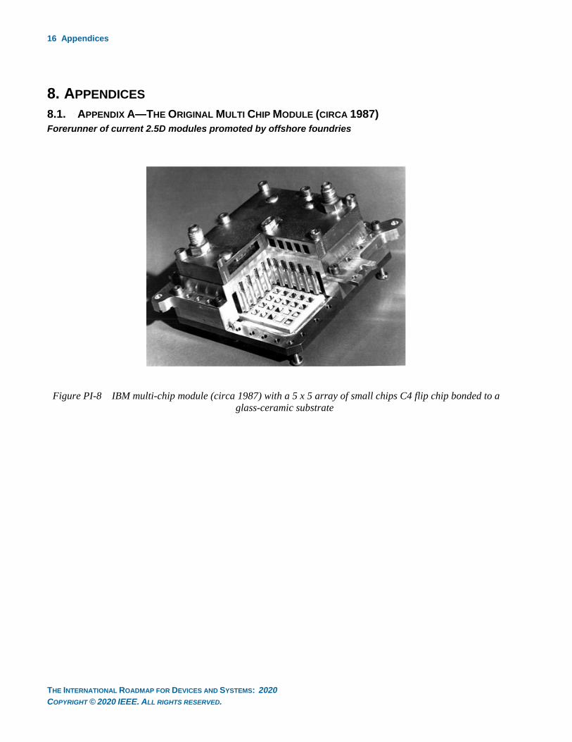
8. APPENDICES 8.1. APPENDIX A—THE ORIGINAL MULTI CHIP MODULE (CIRCA 1987) Forerunner of current 2.5D modules promoted by offshore foundries
Figure PI-8 IBM multi-chip module (circa 1987) with a 5 x 5 array of small chips C4 flip chip bonded to a glass-ceramic substrate

Appendices 17
THE INTERNATIONAL ROADMAP FOR DEVICES AND SYSTEMS: 2020 COPYRIGHT © 2020 IEEE. ALL RIGHTS RESERVED.
8.2. APPENDIX B—SUBSTRATE AND I/O DENSITY ROADMAP (PER INTEL CIRCA 2017)
Figure PI-9 Substrate and I/O density roadmap (per Intel circa 2017)

18 Appendices
THE INTERNATIONAL ROADMAP FOR DEVICES AND SYSTEMS: 2020 COPYRIGHT © 2020 IEEE. ALL RIGHTS RESERVED.
8.3. APPENDIX C—ALTERNATIVE 2D, 2.5D AND 3D PACKAGE CONFIGURATIONS
Figure PI-10 Planar DIMM
Figure PI-11 PoP
Figure PI-12 2.5D Planar on fine-pitch Si substrate (as used for FPGAs from immature fab process)
Figure PI-13 CPU and separate 3D stack of DRAM (as used for a growing number of high performance modules for game systems, servers, AI engines, etc.)

Appendices 19
THE INTERNATIONAL ROADMAP FOR DEVICES AND SYSTEMS: 2020 COPYRIGHT © 2020 IEEE. ALL RIGHTS RESERVED.
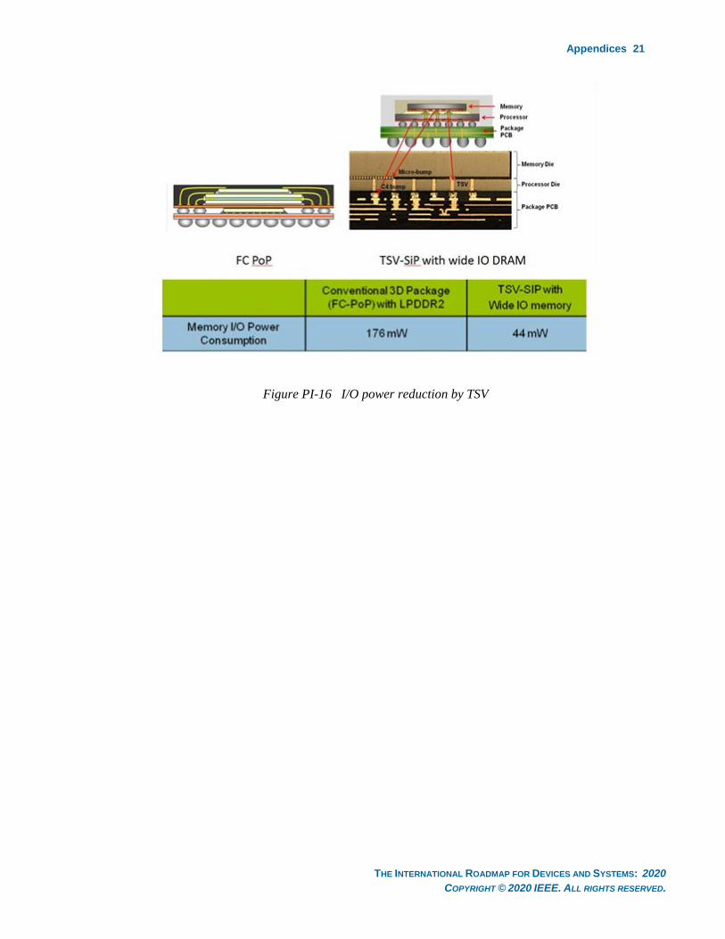
8.4. APPENDIX D—EFFECT OF PACKAGE PENALTIES ON POWER LOSS AND BANDWIDTH
Equations:
Bandwidth, B
B = n* T * f (1)
Where:
n is the no. of signal lines
T is the Toggle Rate ( = 2 for DDR memories )
f is the frequency
Increasing n ( e.g., from 32 bit to 64 bit or all the way up to Wide I/O ) allows maintaining the
Bandwidth B even at a lower frequency and reduce the chance of Bit Errors
P, the Power to drive I/O through Package
P = n * T * f * C * V2 (2)
where,
C is the interconnect capacitance ( = C pkg )
V is peak voltage ( Vdd )
but B, the Bandwidth
B = n* T * f (1)
P, can be re-written as
P = B * C * V2 (3)
So, P is directly proportional to Bandwidth B
The only way to reduce Power Loss P at a constant Bandwidth B, is by reducing C or lowering the
Vdd.
Increasing n, the no. of I/O at a constant B ( as in some PoP Package designs now under
development ) w/o reducing C or V does not help.

20 Appendices
THE INTERNATIONAL ROADMAP FOR DEVICES AND SYSTEMS: 2020 COPYRIGHT © 2020 IEEE. ALL RIGHTS RESERVED.
Signal Integrity as function of I/O Capacitance
(1) In a PoP package ( substrate interconnect Capacitance C of 500 ff ) operating at a Clock Rate
of 800 MHz and delivering a Bandwidth of 6.4 GBps
Figure PI-14 Some oscillations at both logic “high” and “low” levels but still usable for digital operation
(2) In a 3d Stack interconnected by 512 Wide I/O using TSVs ( interconnect Capacitance C < 75 fF )
delivering a Bandwidth of 12.8 GBps at a Clock Rate of just 200 MHz
Figure PI-15 The use of TSVs produces very sharp and clean output waveform at 200 MHz
Appendices 21
THE INTERNATIONAL ROADMAP FOR DEVICES AND SYSTEMS: 2020 COPYRIGHT © 2020 IEEE. ALL RIGHTS RESERVED.
Figure PI-16 I/O power reduction by TSV

22 Appendices
THE INTERNATIONAL ROADMAP FOR DEVICES AND SYSTEMS: 2020 COPYRIGHT © 2020 IEEE. ALL RIGHTS RESERVED.
Table PI-1 3D Package Performance