30 march 2005 draft with changes by sam, marco, and herb
TRANSCRIPT

INTERNATIONAL TECHNOLOGY ROADMAP
FOR SEMICONDUCTORS
2009 EDITION
FRONT END PROCESSES
THE ITRS IS DEVISED AND INTENDED FOR TECHNOLOGY ASSESSMENT ONLY AND IS WITHOUT REGARD TO ANY COMMERCIAL CONSIDERATIONS PERTAINING TO INDIVIDUAL PRODUCTS OR EQUIPMENT.

Front End Processes 1
TABLE OF CONTENTS Front End Processes.............................................................................................................1
SCOPE ............................................................................................................................................1 Difficult Challenges..........................................................................................................................2
The Future of MOSFET – New Materials and New Structures ....................................................................2 Technology Requirements and Potential Solutions .........................................................................4
Logic Devices – High Performance (HP), Low Operating Power (LOP), and Low Standby Power (LSTP) ..........................................................................................................................................................4 DRAM Devices .............................................................................................................................................6 Non-volatile Memory (Flash) ........................................................................................................................7 Phase Change Memory..............................................................................................................................12 Ferroelectric Random Access Memory (FeRAM) ......................................................................................15 Starting Materials .......................................................................................................................................17 Front End Surface Preparation ..................................................................................................................23 Thermal/Thin Films, and Doping ................................................................................................................27 Doping Technology ....................................................................................................................................30 Front End Etch Processing.........................................................................................................................34 Shallow Trench Isolation Chemical-mechanical Planarization (STI CMP) ................................................37
Cross-Cut Issues ...........................................................................................................................39 Inter-Focus ITWG Discussion........................................................................................................39 Impact of Future Emerging Research Devices ..............................................................................39
FEP Metrology Cross-Cut Issues...............................................................................................................40 FEP Modeling and Simulation Cross-Cut Issues .......................................................................................40 FEP Environment, Safety, and Health Cross-Cut Issues...........................................................................41
Conclusion.....................................................................................................................................41 References ....................................................................................................................................42
LIST OF FIGURES Figure FEP1 Front End Process Chapter Scope.......................................................................1 Figure FEP2 CMOS Scaling Enabled through Novel Architecture
(Planar To Non-Planar) and Associated Module Level Challenges .....................5 Figure FEP3 Continued Scaling Pathway in Non-Planar Devices.............................................5 Figure FEP4 DRAM Potential Solutions ....................................................................................7 Figure FEP5 Minimum Feature Size of NAND Flash Memory...................................................7 Figure FEP6 Minimum Feature Size of NOR Flash Memory.....................................................8 Figure FEP7 Flash Memory Interpoly Dielectric Thickness Scaling at
<25nm for NAND Flash ........................................................................................9 Figure FEP8 Schematics of STI Isolation Trenches ..................................................................9 Figure FEP9 Evolution of the STI Aspect Ratio for Flash Memories
with the Minimum Feature Size ..........................................................................10 Figure FEP10 Flash Non-Volatile Memory Floating Gate Potential Solutions.......................11 Figure FEP11 Amorphous / Poly-crystal Phases of a Chalcogenide Alloy,
usually Ge2Sb2Te5 (GST) ...............................................................................13
THE INTERNATIONAL TECHNOLOGY ROADMAP FOR SEMICONDUCTORS: 2009

2 Front End Processes
Figure FEP12 Resistance Change of GST............................................................................13 Figure FEP13 Set/Reset Thermal Cycles to Change the Crystal Phase
of the GST Material and to Write/Erase the PCM...........................................13 Figure FEP14 FeRAM Potential Solutions.............................................................................17 Figure FEP15 Starting Materials Potential Solutions.............................................................22 Figure FEP16 Front End Surface Preparation Potential Solutions ........................................26 Figure FEP17 Thermal/Thin Film Potential Solutions............................................................29 Figure FEP18 Doping Potential Solutions .............................................................................33 Figure FEP19 Etch Potential Solutions..................................................................................35 Figure FEP20 Difficult Challenges and Potential Solutions for STI CMP ..............................38
LIST OF TABLES Table FEP1 Front End Processes Difficult Challenges ............................................................2 Table FEP2 High Performance Device Technical Requirements.............................................2 Table FEP3 Low Operating Power Device Technical Requirements .......................................2 Table FEP4 Low Standby Power Devices Techical Requirements ..........................................2 Table FEP5 DRAM Stacked Capacitor Technology Requirements..........................................6 Table FEP6 Floating Gate FLASH Non-volatile Memory Technology Requirements ..............7 Table FEP7 Charge Trapping FLASH Non-volatile Memory Technology Requirements .......12 Table FEP8 Phase Change Memory (PCM) Technology Requirements ...............................14 Table FEP9 FeRAM Technology Requirements ....................................................................15 Table FEP10 Starting Materials Technology Requirements.................................................17 Table FEP11 Surface Preparation Technology Requirements.............................................23 Table FEP12 Thermal, Thin Film, Doping Process Technology Requirements ...................27 Table FEP13 Etching Process Technology Requirements...................................................34 Table FEP14 CMP Process Technology Requirements.......................................................37
THE INTERNATIONAL TECHNOLOGY ROADMAP FOR SEMICONDUCTORS: 2009

Front End Processes 1
FRONT END PROCESSES SCOPE The Front End Processes (FEP) Roadmap focuses on future process requirements and potential solutions related to scaled field effect transistors (MOSFETs), DRAM storage capacitors, and non-volatile memory (Flash, Phase-change, and ferroelectric). The purpose of this chapter is to define comprehensive future requirements and potential solutions for the key front end wafer fabrication process technologies and the materials associated with these devices. Hence, this Roadmap encompasses the tools, and materials, as well as the unit and integrated processes starting with the silicon wafer substrate and extending through the contact silicidation processes and the deposition of strain layers (pre-metal dielectric deposition and contact etching is covered in the Interconnect chapter). The following specific technology areas are covered: logic devices, including high performance, low operating power, and low stand-by power; memory devices, including DRAM, flash, phase-change, and FeRAM; starting materials; surface preparation; thermal/thin films/doping; plasma etch; and CMP.
A forecast of scaling-driven technology requirements and potential solutions is provided for each technology area. The forecasted requirements tables are model-based unless otherwise noted. The identified potential solutions serve to benchmark known examples of possible solutions, and are intended for other researchers and interested parties. They are not to be considered the only approaches. Indeed, innovative, novel solutions are sought, and their need is identified by red colored regions of the requirements tables.
Some FEP-related topics are presented in other sections of this Roadmap. The scaled device performance and structures forecasts that drive FEP requirements are covered in the Process Integration, Devices, and Structures (PIDS) chapter. The crosscut needs of FEP are covered in the following chapters: Yield Enhancement; Metrology; Environment, Safety, & Health; and Modeling & Simulation. FEP factory requirements are covered in the Factory Integration chapter.
Figure FEP1 Front End Process Chapter Scope
BC
FJ I
A
G H
DE
A: Starting Material B: Isolation C: Well Doping D: Channel Surface (Preparation) E: Channel Doping and Channel Strain F: Gate Stack (Including Flash) and Spacer G: Extension Junction and Halo H: Contacting Source/Drain Junction I: Elevated Junction and Contacts J: DRAM, Phase Change, and FeRAM Storage
THE INTERNATIONAL TECHNOLOGY ROADMAP FOR SEMICONDUCTORS: 2009

2 Front End Processes
DIFFICULT CHALLENGES THE FUTURE OF MOSFET – NEW MATERIALS AND NEW STRUCTURES MOSFET scaling has been the primary means by which the semiconductor industry has achieved the historically unprecedented gains in productivity and performance quantified by Moore’s Law. These gains have traditionally been paced by the development of new lithography tools, masks, photoresist materials, and critical dimension etch processes. In the past several years it has become clear that despite advances in these crucial process technologies and the resultant ability to produce ever-smaller feature sizes, front end process technologies have not kept pace, and scaled device performance has been compromised. To stay on the performance curve, new materials have now been put into production for transistor gate stack fabrication. Within the next several years we expect to see the introduction of additional new materials to increase channel mobility as well as new approaches to device structure, such as fully-depleted SOI (FDSOI) and/or non-planar multi-gate devices.
Material-limited device scaling has placed new demands on virtually every front end material and unit process, starting with the silicon wafer substrate and encompassing the fundamental planar CMOS building blocks and memory storage structures. In addition, the end of planar bulk CMOS is becoming visible within the next several years. As a consequence we must be prepared for the emergence of CMOS technology that uses non-conventional MOSFETs or alternatives such as planar FDSOI devices and dual- or multi-gate devices either in a planar of vertical geometry. An overview of the device alternatives is presented in the Emerging Research Devices chapter. Projections for the manufacturing introduction of non-conventional MOSFET devices are 2013-2015 for FDSOI and/or multi-gate. The challenges associated with integration of these diverse new materials and structures are the central theme of the FEP difficult challenges summarized in Table FEP1.
Table FEP1 Front End Processes Difficult Challenges High-κ gate dielectric with metal gate electrode is now used in production by at least one high-performance logic manufacturer and is expected to be introduced into production by more manufacturers in the 2009-2010 timeframe. Continued scaling of equivalent oxide thickness (EOT) below 0.8nm while preserving electrical performance and reliability will be a challenge. Channel strain engineering to increase mobility was introduced to manufacturing several years ago and is an integral part of MOSFET transistor scaling now and in the future. Continued improvement in strain engineering and application to new device structures is identified as an FEP difficult challenge.
Continued transistor performance scaling is expected to require the replacement of planar CMOS devices with non-classical devices which includes fully depleted planar devices in our analysis. The introduction of these devices will require the replacement of bulk silicon substrates with ultra-thin, silicon-on-insulator (SOI) substrates and double- or multi-gate devices. The transition from extended bulk CMOS to non-classical device structures is not expected to take place at the same time for all applications and all chip manufacturers. Instead, a scenario is envisioned where a greater diversity of technologies are competitively used at the same point in time—some manufacturers choosing to make the transition to non-classical devices earlier, while others emphasize extensions of bulk technology. This is reflected in the High-Performance and Low-Power Device Technology Requirements Tables FEP2, FEP3 and FEP4, by the projection of requirements for multiple approaches in the transition years from 2013 through 2019.
Table FEP2 High Performance Device Technical Requirements
Table FEP3 Low Operating Power Device Technical Requirements
Table FEP4 Low Standby Power Devices Technical Requirements The introduction of new materials is also expected to impose added challenges to the methods used to dope and activate silicon. Series resistance is critical in the near term and needs to be addressed to achieve the goals through 2015. It should be noted that series resistance becomes even more critical when alternate device options [FDSOI, multigate] are considered. In addition to the scaling imposed need for producing very shallow highly activated junctions, the limited thermal stability of most high-κ materials is expected to place new boundaries on thermal budgets associated with dopant activation. In a worst-case scenario, the introduction of these materials could have a significant impact on the overall CMOS process architecture.
THE INTERNATIONAL TECHNOLOGY ROADMAP FOR SEMICONDUCTORS: 2009

Front End Processes 3
In the memory area, stand-alone DRAM device manufacturing has narrowed to the stacked capacitor approach. Therefore, the Technology Requirements table and text for DRAM trench capacitor has been removed and the DRAM section is implicitly aimed at stacked capacitor technologies alone. High-κ materials are now in production for DRAM capacitors using metal-insulator-metal (MIM) structures. It is expected that high-κ materials will be required for the floating gate Flash memory interpoly dielectric by 2012 and for tunnel dielectric by 2013. FeRAM will make a significant commercial appearance where ferroelectric and ferromagnetic storage materials would be used. The introduction of these diverse materials into the manufacturing mainstream is viewed as important difficult challenges. In addition, phase-change memory (PCM) devices are expected to make a commercial appearance by 2010.
In starting materials, it is expected that alternatives to bulk silicon such as silicon-on-insulator substrates will proliferate. Additionally, various forms of strained silicon technology have been adopted for high performance designs and continue to be principally achieved through value-added modifications to the IC manufacturing process. Such bulk alternatives generally imply process architecture changes that impact FEP. Also, an important difficult challenge expected to emerge within this 2009 Roadmap horizon is the need for the next generation 450 mm silicon substrate. Such a diameter move is indicated to maintain pace with historic productivity enhancements based on augmented transistor count performance enhancements. There are concerns whether the incumbent techniques for substrate production can be cost-effectively scaled to the next generation. There are indications that mere scaling of the incumbent techniques alone will not be sufficient. It is also uncertain whether this substrate will be bulk silicon or SOI and whether strained silicon will be the required active layer material. Therefore, the search for potential substrate alternatives presents an important research need. Based upon historical diameter change cycles, the industry is already several years behind the pace necessary to allow the next generation 450 mm silicon substrate to be ready for device manufacture in the year 2014.
Front end cleaning processes will continue to be impacted by the introduction of new front end materials such as high-κ dielectrics, metal gate electrodes, and mobility-enhanced channel materials. Scaled devices are expected to become increasingly shallow, requiring that cleaning processes become completely benign in terms of substrate material removal and surface roughening. Scaled and new device structures will also become increasingly fragile, limiting the physical aggressiveness of the cleaning processes that may be employed. In addition, these new device structures will require precise cleaning and characterization of vertical surfaces. DRAM storage capacitor structures will show increasing aspect ratios making sidewall contamination removal increasingly difficult. Also, there is a challenge for particle scanning technology to reliably detect particles smaller than 28 nm on a wafer surface for characterization of killer defect density and to enable yield learning.
The gate dielectric has emerged as one of the most difficult challenges for future device scaling. Long-term scaling of high-κ stacks below 0.7–0.6 nm EOT remains a major challenge. The gate electrode also represents a major challenge for future scaling, where work function, resistivity, and compatibility with CMOS technology are key parameters for the new candidate gate electrode materials especially when the industry introduces new channel materials or non-planar devices. Another very difficult challenge in device scaling is channel mobility enhancement, making mechanical stress a first-order consideration in the choice of front end materials and processes. In order to maintain high device drive currents, technology improvements are required to increase channel mobility of traditional bulk CMOS devices, as well as partially depleted-, and fully depleted SOI devices, and eventually on to non-planar devices. Additional challenges include continued scaling and abruptness of shallow junctions, parasitic resistance, and contact silicidation. A dominant problem for continued scaling is posed by process and materials variability; especially that arising from placement of dopant atoms and their final location. These challenges and potential solutions are discussed in more details under the Thermal, Thin Films, and Doping Processes section of this chapter.
The persistent challenge in scaling device sizes is the control of gate length critical dimensions (CD). Etching uniformity all the way to the wafer edge is a particularly difficult issue. As gate CD shrinks, the presence of line width roughness (LWR) is becoming the biggest portion of CD variation at 28nm technology node and beyond. The LWR is at best staying constant as the line width shrinks, which makes it a major scaling concern. Current methods of quantification need to be standardized to allow the industry to address the problem. The choice of photoresist type, etch bias power, and etch chemistry are critical for keeping low LWR. With high-κ dielectrics and metal gates going into production, etch processes with sufficient selectivity and damage control for use with these materials have been identified. As non-planar transistors become necessary, etch becomes much more challenging. FinFET configurations bring new constraints to selectivity, anisotropy, and damage control.
Chemical-Mechanical Planarization (CMP) is becoming more important for Front End Processing. Having been used for several years in the formation of shallow trench isolation, its use in the Front End is expanding, especially in the
THE INTERNATIONAL TECHNOLOGY ROADMAP FOR SEMICONDUCTORS: 2009

4 Front End Processes
manufacture of memory devices and in the implementation of gate-last metal gate integration schemes. Uniformity, selectivity, and pattern density dependency continue to be challenges for CMP processes.
TECHNOLOGY REQUIREMENTS AND POTENTIAL SOLUTIONS LOGIC DEVICES – HIGH PERFORMANCE (HP), LOW OPERATING POWER (LOP), AND LOW STANDBY POWER (LSTP) The scaling roadmap for high performance (HP), low operating power (LOP) and low standby power (LSTP) technologies are captured as separate tables in the 2009 ITRS FEP update. This categorization in separate tables becomes more relevant as the technology options (and scaling roadmap) for performance and power are starting to vary rather significantly for future device generations. For example, the advanced high-κ/metal gate stack technology appears imperative for high performance devices in 2009 and beyond, while conventional SiON/Poly may still be the mainstream choice for LSTP devices through 2011. Also, by capturing the scaling pathway for HP, LOP, and LSTP in different tables, we can address the specific module level scaling challenges associated with the technologies for performance and/or power.
Tables FEP2, FEP3 and FEP4 show the scaling pathway for HP, LOP and LSTP respectively, for near-term and long-term years. For each of the tables, the Vcc scaling scenario (to keep with the active power scaling challenge) and Ion as well as Ioff requirements are captured for near and long-term years. These are consistent with the PIDS estimates and drive the choice of module options for each device type.
For high performance, it appears that the increasing drive current needs will challenge the ability to aggressively scale EOT, as well as the ability to deliver higher levels of strain for enhanced injection velocity of electrons and holes. Also, stringent controls in doping technology are needed to maintain short channel effects and keep Ioff within the 100nA/micron limit. Although high-κ/metal gates are already in high volume production, the scaling potential of these stacks below 0.7nm EOT (with acceptable leakage current) is questionable. Also, maintaining short channel control for continued gate length scaling may drive introduction of non-planar architectures and/or scaled SOI schemes as captured in the table.
For LOP scaling, the Ion/Ioff requirement calls for a relaxed EOT target with lower gate leakage requirement as shown in Table FEP3. The need to deliver performance at lower operating power (low Vcc) calls for excellent short channel control and possible use of strain enhanced performance in future device generations. Aggressive scaling of Vcc appears very challenging due to the increasing concerns with variability. The advent of non-planar structures (and FDSOI) will help reduce the variability caused by random dopant fluctuations and will provide better short channel control delivering the needed Ion/Ioff.
For LSTP scaling, the low Ioff requirement allows for thicker EOT with low gate leakage as shown in Table FEP4. Introduction of High-κ/Metal gate appears imminent beyond 2011, and this will help provide an aggressive EOT scaling pathway for similar Ioff requirements. Achieving the low Ioff requirement (100 pico-amp/micron) at scaled physical gate length is a challenge while concurrently forming ultra shallow junctions with low leakage (as captured in Table FEP12). Here again, the introduction of multiple gate devices and/or FDSOI appears imminent to continue to deliver the needed Ion/Ioff with scaling.
Note: The cost of ownership for introduction of options is NOT considered in these tables. While we acknowledge that the choice of process options for scaling can be significantly influenced by the cost of ownership, it is complicated to factor in to the Tables FEP2, FEP3, and FEP4.
It is important to note that future scaling of CMOS relies specifically on introduction of new materials (example: high-κ/metal gates, novel alloyed-silicides, low-κ spacers, etc.) and/or device architecture (FDSOI, multigate FETs, nanowires, etc.). Figure FEP2 shows a schematic of the module level challenges for planar and mugFETs and Figure FEP3 captures the potential scaling pathway (or potential solutions) for continued scaling to deliver the device requirements for HP, LOP, and LSTP technologies.
THE INTERNATIONAL TECHNOLOGY ROADMAP FOR SEMICONDUCTORS: 2009

Front End Processes 5
Figure FEP2 CMOS Scaling Enabled through Novel Architecture (Planar To Non-Planar) and
Associated Module Level Challenges This rapid introduction of new materials and device structures in the next five to seven years constitutes an unprecedented multiplicity of challenges to develop, and also to integrate these developments into effective, cost-efficient production technologies. During this period of transition, the plethora of choices for the device structure seems likely to lead to some divergence within the industry, some companies choosing to aggressive scale bulk CMOS parameters, while others make the transition to FDSOI and multi-gate structures where the requirements may be vastly different and at least equally challenging.
The process module level scaling targets that are needed to meet the HP, LOP, and LSTP device requirements (Tables FEP2, FEP3, and FEP4), are highlighted in the Thermal/Thin Films Doping (TTFD) Process Technology Requirements section below. Also, potential solutions for specific process modules are discussed within the TTFD Section.
Figure FEP3 Continued Scaling Pathway in Non-Planar Devices
THE INTERNATIONAL TECHNOLOGY ROADMAP FOR SEMICONDUCTORS: 2009

6 Front End Processes
DRAM DEVICES DRAM capacitor technology is now more seriously challenged than any other previous period due to the accelerated scaling of cell size. Table FEP5 shows a summary of technology requirements for DRAM capacitor. Since capacitors were introduced into DRAM, the required capacitance has nearly remained constant at about 25fF/cell. However, it is required that the cell capacitance is controlled as a key requirement after 2012. This new challenge will be realized by buried bit line or buried word line technology resulting in reducing the parasitic capacitance, which can also decrease the required capacitance down to 20fF/cell instead of the previous 25fF/cell. This capacitance could also be further lowered by suppression of parasitic capacitance by improving the performance of buried bit line or by buried word line technology.
Table FEP5 DRAM Stacked Capacitor Technology Requirements
As cell critical dimension decreases down to 20nm, the most difficult situation faced is that there will not be enough space for the deposition of the dielectric layers and the plate electrode because of an extremely limited area. Generally, as the physical thickness of the dielectric and metal layers decreases, physical properties such as the dielectric constant and the work function are degraded. In addition to that, when the dielectric constant increases the physical thickness that can provide the required low leakage current also increases. In other words, the higher the dielectric constant is, the more difficult it is to fabricate a capacitor due to the increased physical thickness of the dielectric film. Therefore the most difficult challenge will be the restriction in physical thickness of dielectric layer and electrode layer. That is because the high dielectric constant and high work function must be maintained even at an ultimate film thickness of about 5nm-7nm. This physical constraint is the main reason driving an ultra high aspect ratio storage node rather than the electrical properties of the dielectric and electrode. It is projected that the required capacitance will be realized not only by improved dielectrics but also other potential solutions such as high work function electrode materials or by an ultra high aspect ratio storage node, slowing the need to increase dielectric constant, which results in slowing the increase of physical thickness.
Figure FEP4 shows the potential solutions for DRAM stacked capacitor. The 20nm generation will surely be very important in terms of new dielectrics and electrode materials. As for the dielectrics, the cell-capacitance and area-scaling will introduce a tradeoff under the constraint of the gate dielectric leakage. It is expected that at around 20nm the capacitor will be based around ZrO2 dielectrics. This is driven by the requirement for a dielectric constant of around 50, which provides 0.6nm equivalent oxide thickness (Teq). Possible routes to ZrO2-based dielectrics of 0.6nm may be by modification of deposition conditions or by material modification of the ZrO2 and TiN layers. When the DRAM pitch goes down below 20nm, Teq is required to be less than 0.45nm. This will require a new kind of high-κ material with a dielectric constant of 60~70. While such a dielectric constant can be obtained from TiO2, Ta2O5, STO, or BST, it should be noted that this high-κ path is limited by the physical thickness under the requirement of a fixed refresh time, thus there is a need to find other capacitance sources in the DRAM cell structure.
TiN will continue to be used as an electrode material until the 28nm generation by maximizing the work function and step coverage and minimizing the degradation of dielectrics during deposition. New deposition technology and material modification needs to be developed for the currently used TiN. Beyond the 20nm generation, new electrode materials such as Ru, RuO2, Ir, IrO2, or SrRuO3 need to be considered from the viewpoint of work function and enhancement of crystallization for the dielectric layer. Besides the electrical characteristics of the electrode material, one thing to note is the limitation in physical thickness. Taking into consideration that the work function or crystalline structure can change as the electrode material gets very thin, the formation technology for ultra thin layers which still have high work function, will be a challenging issue. Beyond the 13nm generation, crystalline structure of the bottom electrode material will have to be considered as well as the work function because high-κ oxides such as STO or BST can be modulated in terms of crystalline content which results in changes to the dielectric constant. For this reason, perovskite conducting oxides such as SrRuO3 need to be considered with STO or BST.
Besides the high-κ dielectrics and high work function electrode, new technologies for storage node formation with ultra high aspect ratios are needed in combination with the required Teq. Therefore, new oxide etching technology for ultra high storage node also needs to be developed.
As cell size shrinks, the 3D structures on which dielectric films and plate electrode layers are deposited will get much deeper and narrower. So, atomic layer deposition (ALD) will have to be enhanced by improving the process performance such as step coverage and throughput. More technically difficult issues for ALD beyond the 13nm
THE INTERNATIONAL TECHNOLOGY ROADMAP FOR SEMICONDUCTORS: 2009

Front End Processes 7
generation are driven by the need for multi component films such as BST (BaSrTiO3) or SrRuO3, while maintaining stoichiometry as well as step coverage using precursors with poor reactivity. So, efforts to develop highly reactive ALD precursors need to be pursuedFEP1.1
First Year of IC Production 2009 2010 2011 2012 2013 2014 2015 2016 2017 2018 2019 2020 2021 2022 2023 2024
DRAM 1/2 pitch (nm) 52 45 40 36 32 28 25 22 20 18 16 14 13 11 10 8.9Top Electrode Ru, RuO2, Ir, IrO2
Capacitor Dielectric Material TiO2, STO, BSTBottom Electrode Ru, RuO2, Ir, IrO2 SrRuO3
ZrO2, HfO2, Ta2O5TiN
TiN
Figure FEP4 DRAM Potential Solutions
NON-VOLATILE MEMORY (FLASH) Table FEP6 summarizes the main technology requirements for NOR and NAND flash memories. The most important issues are related to the cell area reduction (see the non-volatile memory technology requirements, in the PIDS chapter) and to the consequent scaling down of the thickness of the two key active dielectrics of the memory cell, namely the tunnel oxide and the interpoly dielectric, in a way that guarantees the charge retention and endurance requirements for the memory cell. For NAND Flash the best definition of the minimum feature size is the half-pitch of the memory cell when viewing a cross section parallel to the bit line, which is also the half pitch of the poly 2-word line. Refer to Figure FEP5.
Figure FEP5 Minimum Feature Size of NAND Flash Memory
Table FEP6 Floating Gate FLASH Non-volatile Memory Technology Requirements
THE INTERNATIONAL TECHNOLOGY ROADMAP FOR SEMICONDUCTORS: 2009

8 Front End Processes
For NOR Flash memories the definition of the minimum feature size is difficult and can vary among the different Flash manufacturers. Referring to Figure FEP6, the following are definitions of the minimum feature size specific for NOR Flash memories, as follows:
• The half pitch when viewing a cross section parallel to the poly 2 word line • The poly 1 to poly 1 distance along the word line • The minimum contact size
contact
active& poly1
Metal1
poly2
contact
active& poly1
Metal1
poly2
poly1active area
contact
Metal 1
cell pitchhalf pitch
poly2cross section along the word line
top view of 2 memory cells
contact
active& poly1
Metal1
poly2
contact
active& poly1
Metal1
poly2
poly1active area
contact
Metal 1
cell pitchhalf pitch
poly2cross section along the word line
top view of 2 memory cells
contact
active& poly1
Metal1
poly2
contact
active& poly1
Metal1
poly2
poly1active area
contact
Metal 1
cell pitchhalf pitch
poly2cross section along the word line
contact
active& poly1
Metal1
poly2
contact
active& poly1
Metal1
poly2
contact
active& poly1
Metal1
contact
active& poly1
Metal1
poly2
contact
active& poly1
Metal1
poly2
contact
active& poly1
Metal1
poly2
contact
active& poly1
Metal1
contact
active& poly1
Metal1
poly2
poly1active area
contact
Metal 1
cell pitchhalf pitch
poly2cross section along the word line
poly1active area
contact
Metal 1
cell pitchhalf pitch
poly2
poly1active area
contact
Metal 1
cell pitchhalf pitch
poly2
poly1active area
contact
Metal 1
cell pitchhalf pitch
poly1active area
contact
Metal 1
cell pitchhalf pitch
poly2cross section along the word line
top view of 2 memory cells
Figure FEP6 Minimum Feature Size of NOR Flash Memory
The tunnel oxide thickness must be reduced for the programming/erasing performances while scaling the interpoly dielectric thickness reduction is necessary to keep the capacitance coupling ratio, αg, at an almost constant value in order to achieve acceptable ratios between the control and floating gate voltages. The coupling ratio is typically improved by reducing the interpoly dielectric thickness and increasing the tunnel oxide thickness and the floating/control gate coupling area. Scaling the tunnel oxide thickness is one of the key challenges for Flash memories, since this dielectric must simultaneously guarantee good charge retention properties that are better with a higher thickness, and high write/erase performance that is better with a lower thickness.
The impact of the floating/control gate coupling area on the αg factor becomes a critical issue starting from 25 nm technology for NAND flash devices, when the spacing between two adjacent floating gates (poly 1) becomes too small to allow the control gate (poly 2) to overlap the vertical poly 1 sidewalls, as is done in the present architecture. The lack of electrical coupling between poly 1 and poly 2 along the vertical sidewalls of the poly 1 results in a strong degradation of the αg value and could require a strong reduction of the interpoly dielectric thickness as a compensation. This situation is illustrated in Figure FEP7.
THE INTERNATIONAL TECHNOLOGY ROADMAP FOR SEMICONDUCTORS: 2009

Front End Processes 9
Poly 1
Poly 1
Poly 2 IPD
Poly 2
Poly 2
IPD
IPD
65 nm
60-80 nm
Poly 1
Poly 1
Poly 2 IPD
Poly 2 IPD
Decoupling
40-60 nm
45 nm 10-15 nm EOT
5-6 nm EOT
Figure FEP7 Flash Memory Interpoly Dielectric Thickness Scaling at <25nm for NAND Flash
The present interpoly dielectric technology is based on oxy-nitride stacked layers and will probably not be feasible for aggressive reduction of equivalent oxide thickness (EOT), due to unacceptable charge retention properties. Thus, the introduction of high-κ materials at this step will be necessary. Alternatively, new floating gate designs to maintain a high coupling area with the control gate or storage materials different from poly-silicon are potential solutions. From this point of view, the 25–22 nm technology generation for NAND will be a transition one with both classical and new solutions depending on the architecture schemes chosen for the memory cells.
Another challenge for the Flash memory scaling is the formation of shallow trench isolation (STI). The continuous scaling of the dimensions along the X axis (along the word line in Figure FEP5) and the necessity to maintain the depth of the STI trench cause an increase of the trench aspect ratio that needs to be filled with the STI oxide. (Figures FEP8 and FEP9). In response to these challenges an overview of the Flash memory Potential Solutions is shown in Figure FEP10.
A
B
A
B
A
B
A
B
Figure FEP8 Schematics of STI Isolation Trenches
The aspect ratio is defined as the B/A ratio, including both the depth of the trench inside silicon and the height of the stack deposited on the silicon surface. The factor A is based on the minimum feature size F while the factor B depends on the type of isolation scheme utilized.
THE INTERNATIONAL TECHNOLOGY ROADMAP FOR SEMICONDUCTORS: 2009

10 F
THE
ront End Processes
INTERNATIONAL TECHNOLOGY ROADMAP FOR SEMICONDUCTORS: 2009
Filling high aspect ratio trenches with the isolation oxide is a major challenge to be faced. Additional challenges for isolation include the overall thermal budget in the STI formation, especially in the case of self-aligned STI schemes, and the co-existence of different STI trench geometries on different parts of the chip (memory array versus I/O circuitry).
Figure FEP9 Evolution of the STI Aspect Ratio for Flash Memories with the Minimum Feature Size
0.0
5.0
10.0
15.0
20.0
020406080
F (nm)
A.R.
Worst case NANDBest Case NANDWorst case NORBest case NOR

Front End Processes 11
THE INTERNATIONAL TECHNOLOGY ROADMAP FOR SEMICONDUCTORS: 2009
First Year of IC Production 2009 2010 2011 2012 2013 2014 2015 2016 2017 2018 2019 2020 2021 2022 2023 2024
FLASH TUNNEL DIELECTRIC Nitrided oxide Oxynitride / high-κ stack
FLASH INTERPOLY DIELECTRIC ONO (Oxide-nitride-oxide) Oxynitride / high-κ stack
FLASH STI FILLING TECHNOLOGY High density plasma CVD Spin-on-dielectric
FLASH GATE ELECTRODE Poly-Si Poly-Si / Metal Metal
This legend indicates the time during which research, development, and qualification/pre-production should be taking place for the solution. Research RequiredDevelopment UnderwayQualification / Pre-ProductionContinuous Improvement
Figure FEP10 Flash Non-Volatile Memory Floating Gate Potential Solutions

12 Front End Processes
CHARGE TRAPPING FLASH MEMORY TECHNOLOGY Challenges for continued scaling of both NOR and NAND devices indicate a future need for an alternative to traditional floating gate technology. Generally, there are more issues in scaling the NOR cell than the NAND cell, however, both suffer from cross-talk effect, which mostly impacts multilevel devices. Moreover, both NOR and NAND Flash memories will face a hard limit in scaling the poly1 to poly1 pitch along the word line, due to the ONO dielectric thickness on the floating gate side wall, as discussed above. Charge trapping memory technology, based on storing charge inside a silicon nitride or a high-k dielectric, can solve these two issues. Table FEP7 summarizes the main technology requirements for charge trapping flash memories.
Table FEP7 Charge Trapping FLASH Non-volatile Memory Technology Requirements
The major advantages of the charge trapping approach are:
• Suppression of floating-gate to floating-gate disturbance • High scalability (feasibility for FinFET structure) • Simple integration for embedded memory applications • Immunity to localized defects in tunnel oxide (ex: SILC effects) reducing challenges to tunnel oxide scaling • Tight erase distributions The most common recognized challenges of the charge trapping approach are:
• Low gate to nitride coupling ratio • High-κ blocking layer between the trapping material and the gate is mandatory • A high work function gate, i.e. a metal gate is mandatory in order to erase the memory cell with reasonable bias • Optimization of charge redistribution retention after cycling related to localized charge storage inside a dielectric. As a consequence of these challenges, some major technology issues must be faced before the charge trapping approach moves into manufacturing, including triggering of the charge trapping material and integration of the high-κ blocking layer and the metal gate.
PHASE CHANGE MEMORY Phase Change Memory (PCM) technology is based on the basic properties of the chalcogenide alloy 1 , so the integration of the material into a standard CMOS process represents a challenging matter: not for the single cell concept, already proven to be very strong, but for the manufacturability of very high density non-volatile memory, where the technology can be considered robust only if demonstrated over many billions of cells. Considering the electronic and transport properties of the chalcogenide alloy, either in the crystalline or in the amorphous state, in order to form a functional compact cell array, a PCM cell is be formed by a variable resistor (heater and chalcogenide – called data-storage) in series with a selector device (transistor). Refer to Figures FEP11, FEP12, and FEP13 for illustrations of the basic concepts involved in inducing the phase change and its desired properties. Hence, the basic PCM cell has a 1T/1R structure. The type of transistor and of data-storage varies respectively as a function of the application and of the process architecture strategy. For high-density memory, a more compact cell layout is achieved via the vertical integration of a pnp bipolar transistor,2, 3 while for embedded memory the transistor is a n-channel MOS, where a larger cell size is balanced by a minimum process cost overhead with respect to the reference CMOS.
1 Chalcogenides are alloys based on the VI group elements that have the interesting characteristic to be stable at room temperature both in the amorphous and in the crystalline phase. In particular, the most promising are the GeSbTe alloys which follow a pseudobinary composition (between GeTe and Sb2Te3), often referred as GST.
THE INTERNATIONAL TECHNOLOGY ROADMAP FOR SEMICONDUCTORS: 2009

Front End Processes 13
Amorphous CrystallineAmorphous Crystalline
High resistivity Low resistivityHigh resistivity Low resistivity
Figure FEP11 Amorphous / Poly-crystal Phases of a Chalcogenide Alloy, usually Ge2Sb2Te5 (GST)
I
V
I
V heater
GST
heater
GST
Figure FEP12 Resistance Change of GST
Time
Temperature
Tx
Tm
Reset (amorphization)
Set (crystallization)
Time
Temperature
Tx
Tm
Reset (amorphization)
Set (crystallization)
Figure FEP13 Set/Reset Thermal Cycles to Change the Crystal Phase of the GST Material
and to Write/Erase the PCM
The integration of the data-storage occurs between the front-end and the back-end of the CMOS process. The “simple” variable resistor, i.e., the heater and chalcogenide system, may be obtained in different ways and the choice is a function of the understanding of the process complexity, current performances, thermal properties and scaling perspective.4 A possible reported approach is to use a sub-lithographic contact heater with a planar chalcogenide5 or a modified version with contact recess and chalcogenide confinement, which should improve the thermal properties and hence reduce the reset current.6
THE INTERNATIONAL TECHNOLOGY ROADMAP FOR SEMICONDUCTORS: 2009

14 Front End Processes
A completely different approach relies on the definition of the contact area between the heater and the chalcogenide by the intersection of a thin vertical semi-metallic heater and a trench, called a “μtrench,”7 in which the chalcogenide is deposited. Since the μtrench can be defined by sub-litho techniques and the heater thickness by film deposition, the cell performance can be optimized by tuning the resulting contact area still maintaining a good dimensional control. Table FEP8 summarizes the main technology requirements for Phase Change Memories.
Table FEP8 Phase Change Memory (PCM) Technology Requirements
Despite the high potential of the PCM concept and the good integration results so far achieved,8, 9 some practical challenges must still be addressed. In particular, large efforts are being dedicated to the integration of a compact PCM cell structure with the chalcogenide compound, to achieve a full compatibility with an advanced CMOS technology and to reduce the programming current without degrading the appealing features of the PCM technology. The easier integration of PCM cell is achieved with the pillar-like structure, but the resulting programming currents are quite large, thus posing additional constraints on the selecting device and on the overall power consumption. Several approaches so far proposed to reduce the programming currents of PCM devices rely on the confinement of the chalcogenide compounds in trenches,10 , 11 contact recessions,12 or contact holes.13 The main idea is to force the maximum current crowding directly in the active region of the cell, where the chalcogenide material switches between the two phases. In fact, it has been estimated4 that the programming currents can be reduced up to the 50% by employing fully confined structures with the chalcogenide material that fills a contact hole. The superior capabilities of confined structures has been demonstrated by the µTrench PCM cell architecture that achieved a programming current of 450 µA at 180 nm14 and 350 µA at 90 nm. 15 A programming current of 260 µA in a 50 nm contact has been demonstrated for a fully confined structure obtained with a CVD-deposited chalcogenide.16 These results point out that the fabrication of efficient PCM cell architectures will be required to fill confined structures with very high aspect ratio. A continuous improvement of the chalcogenide material minimum conformality is thus expected to support the cell architecture evolutions.
To support reliable large array products, PCM technologies must be able to retain data over the product’s lifetime with very low defect rates. Data retention is limited by resistance loss of the amorphous phase of the material, a process that is controlled by the kinetics of crystallization. Prior work on data retention of reset cells shows that data retention of GST is much longer than ten years at 85°C, and therefore adequate for typical non-volatile memory applications.17, 18 This value is satisfactory to address consumer applications, but it is not matching industrial requirements for high temperature operation (e.g., automotive applications). This drives a need for improvement of the maximum storage temperature. This improvement will mainly come from the development of different chalcogenide compounds and compositions.
One of the most attracting features of PCM technology is the expected superior endurance when program and erase repetitive operation are performed. Several publications reports endurance capabilities that range from 107 up to 1012 cycles. Such impressive results depend on the intrinsic endurance of the chalcogenide compounds as well as on the overall stability of the PCM cell surrounding material. Among them, the heater electrode is the part of the cell that undergoes to the heavier stressing conditions, with temperatures much higher than the 600°C and current densities that can exceed 1 A/μm2. The most important electrical property of the heater material that must be preserved during cycling is the electrical resistivity, which is to remain stable according to the endurance requirement. The maximum resistivity variation is thus intended to provide a guideline on the main electrical property of the heating element in PCM cells, providing the requirement that guaranties to be able, with the same current, to switch the PCM cells among the two logic states for the required number of P/E cycles.
The requirement on the heater resistance stability is intimately related to the maximum reset current density requirement. It has been reported that, under the simple assumption of isotropic scaling, the expected reset current density will increase linearly with the scaling factor,4 and a more aggressive trend could be expected according to the forecasted roadmap. A detrimental effect of this increase could be more aggressive stressing conditions for the heater material and for the chalcogenide-heater interface, which should be faced with a slower growth of the required current density. It follows that a better heating efficiency will be required to downscale the PCM devices that could be achieved through an increase of the heater resistivity, still preserving the stability requirements. It is thus expected that the scaling roadmap of PCM technology will face the need to provide novel material for the heating electrode capable to reach a trade off among the endurance requirements and the performance requirements.
THE INTERNATIONAL TECHNOLOGY ROADMAP FOR SEMICONDUCTORS: 2009

Front End Processes 15
FERROELECTRIC RANDOM ACCESS MEMORY (FERAM) FeRAM (also abbreviated FRAM) was a new addition to the 2001 ITRS, and was the result of collaboration between the FEP and PIDS technology working groups. The critical requirement tables, Table FEP9, was revised in 2009 based on the results of a survey of the FeRAM manufacturers.
Table FEP9 FeRAM Technology Requirements Historically speaking, FeRAM devices had been proposed much earlier than semiconductor memories19. At present however, memory capacity is limited to ~1/1000 of that of commodity DRAM, due to difficulties associated with capacitor fabrication, integration, and reliability. Though these difficulties together with the lack of a “killer application” had constrained commercial production, recently several “killer applications” are proposed. Solid state drive (SSD) is one promising application. In this case, FeRAM acts as page buffer memory instead of DRAM and /or SRAM, thus utilizing FeRAM high speed write/read performance and non volatility. FeRAMs depend substantially on the continued development of materials such as ferroelectric films which make forecasts presented here somewhat speculative. Nevertheless, the roadmap covers the years 2009 to 2024 in order to provide a strategic overview of the technology directions and the challenges that must be overcome. This section consists of 1) mass production based table, 2) mixed-signal devices and feature size, 3) cell size, 4) ferroelectric materials alternatives, 5) minimum switching charge estimation, and 6) endurance.
MASS PRODUCTION BASED TABLE Since the FeRAM table was introduced in 2001, the requirements that have been included in the tables from 2001–2006 reflected FeRAM technology that was presented at conferences because obtaining accurate information on devices in the marketplace was not readily available. As a result, a large gap existed between what FeRAM semiconductor manufacturers presented at conferences and what was commercially available on the market. To eliminate this gap, the requirements for the 2007 table were defined from the manufacturer’s requirements available on their homepage, surveys, and using a previous precedent established for DRAMs, where the level of technology in the roadmap is based upon the two leading manufacturers which have achieved a production volume of at least 10,000 chips per month. The 2009 table is defined as the same manner with the 2007 table based on FeRAM mass production information.
MIXED SIGNAL DEVICES AND FEATURE SIZE As noted above FeRAM technology has lagged behind leading edge memories such as Flash and DRAM. Although this gap exists, manufacturers have developed devices which use advanced CMOS such as 0.13µm technology but use 0.18 µm technology for the Metal 1 half pitch width for FeRAM as shown in Table FEP9. The FeRAM technology node is defined here by Metal 1 half pitch width for this roadmap. Combining advanced CMOS technology with relaxed designed rules for FeRAM, is expected to increase the number of applications for FeRAM. Table FEP9 shows a feature size of 0.18µm for year 2009 commercial product using the same criteria as DRAM. Feature size scaling is forecasted to occur at approximately 0.8× every four years which is at a slower pace than other established memories.
CELL SIZE Currently, the most efficient cell structure is the One Transistor-One Capacitor (1T-1C) cell and it is replacing the 2T-2C cell that is less efficient but offers greater operating range stability as noted in a recent review on FeRAM design.20 However, in the market both cell structures will likely be available for some time depending upon the device application. As far as the capacitor structure is concerned, the change from the planar capacitor type to a stack configuration has resulted in a cell size reduction. The timing of a shift from a stacked structure to a 3D structure will depend upon the ferroelectric material used and it is expected to occur approximately in 2016. The different capacitor configurations are shown in the drawing accompanying Table FEP9. The above-mentioned cell structure and capacitor configuration changes are forecasted to reduce the cell area factor to 16 in years 2013–2015 after which the cell area factor will continue with further scaling. Another path to shrink the cell size is by changing to a one transistor type (1T). Basic research and development are continuing on this topic.
FERROELECTRIC MATERIALS ALTERNATIVES There are several ferroelectric materials under evaluation at the present time21 , but there is no clear, single material choice. The two current materials are PZT, or Pb(Zr,Ti)O3 and SBT, or SrBi2Ta2O9. SBT has superior fatigue-free
THE INTERNATIONAL TECHNOLOGY ROADMAP FOR SEMICONDUCTORS: 2009

16 Front End Processes
characteristics with a Pt bottom electrode and is more suitable for low voltage operation because of its smaller coercive field (Ec). (Fatigue is defined as a loss of polarization or charge that develops after bipolar cycling of the memory capacitor.) PZT has a larger switching charge per unit area, QSW, which is important since it is allows for further scaling without shifting to a 3D cell. Both materials may suffer damage due to process integration during the device fabrication which has hampered device development. The most important issues with PZT and SBT films are suppression of film deterioration that is attributed to hydrogen diffusion 22 and oxygen loss, the achievement of stable data read/write characteristics, and data retention during integration. Process improvements are also required for embedding FeRAM. It is important to avoid high temperature annealing or hydrogen incorporation into ferroelectric films after the oxygen anneal used to crystallize the films. For example, AlOx and TiN are often used as hydrogen barrier layers. Also, conductive oxides such as IrO2 or SrRuO3 (SRO) are often used as capacitor electrode materials for PZT since their use improves ferroelectric capacitor reliability. Physical vapor deposition (PVD) and chemical solution deposition (CSD) including Sol-Gel methods are the most commonly used methods for ferroelectric film deposition. However, continued scaling dictates the need to shift to methods with better step coverage such as MOCVD as noted in Figure 14. A previously reported MOCVD study has shown that a (111) oriented PZT film is very effective at increasing the switching charge.23 Etching of capacitor electrodes remains a challenge with RIE, because the capacitor electrodes do not react to form volatile etch by-products. Therefore, sputter etching is widely used. This limits critical dimension (CD) control and makes scaling more difficult. High temperature etching technology for improving sidewall slope of the capacitor was developed to overcome this difficulty.24 PZT and SBT are often doped to improve their electrical properties. For instance, PZT may be doped with lanthanum and SBT with niobium. Doping is used to achieve the following film enhancements: leakage current suppression, improved endurance or imprint characteristics, suppression of post process film degradation, and others. Besides PZT and SBT, one of the promising new materials is BLT or (Bi,La)4Ti3O12,25 of which characteristics are in-between the foregoing two.26 In addition, BiFeO3 (BFO) has gained much attention as a new candidate material. BFO has a giant ferroelectric polarization of 150μC/cm2 or more.27 Although BFO exhibits a large polarization, it also requires a higher switching voltage which means that the film needs to be thinner or possibility doped to accommodate low voltage operation. Since the ferroelectric properties of each material have improved in recent years due improvement in process technology, it essential for the process to be optimized for the integrated ferroelectric capacitor in order to obtain good ferroelectric properties.
ESTIMATED MINIMUM SWITCHING CHARGE The estimated minimum switching charge has been derived as follows: The sense amplifier for FeRAM is assumed to be basically the same as that of DRAM. Therefore, the bitline signal voltage was calculated using DRAM data from the 1999 ITRS. These data provide that the capacitance Cs remain constant at 25fF/cell independent of technology node, and the bitline capacitance is 320fF at the 0.18 µm node. Based on this data with the further assumption that bitline capacitance is proportional to F2/3, where F is the feature size28 allows for the calculation of ΔVbitline. The ΔVbitline is about 140 mV, and the assumption is that this is needed for the sense amplifier circuit independent on technology nodes. Multiplying ΔVbitline (140 mV) with Cbitline then gives the minimum switching charge.
Dividing the minimum switching charge value derived above by the ferroelectric film switching charge per unit area, QSW, (assumed to be 30 µC/cm2) then yields the desired capacitor area. If this area is larger than the projected capacitor size, then a 3D capacitor should be adopted. Based on this, a 3D capacitor will be needed by year 2017.
The FeRAM forecast of Table FEP9 is based on these assumptions and calculations. “Red brick walls” begin to appear in 2017. The first priority to break through these walls is the development of highly reliable ferroelectric materials that exhibit negligible process induced degradation.
THE INTERNATIONAL TECHNOLOGY ROADMAP FOR SEMICONDUCTORS: 2009
Front End Processes 17
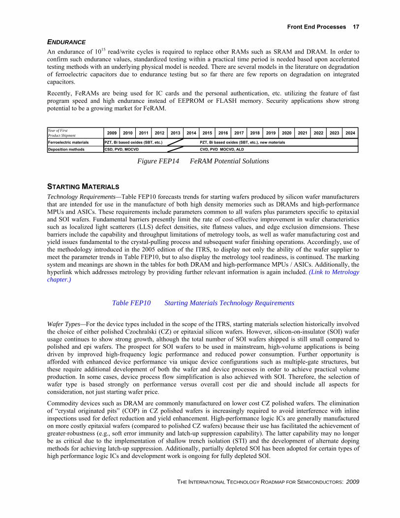
ENDURANCE An endurance of 1015 read/write cycles is required to replace other RAMs such as SRAM and DRAM. In order to confirm such endurance values, standardized testing within a practical time period is needed based upon accelerated testing methods with an underlying physical model is needed. There are several models in the literature on degradation of ferroelectric capacitors due to endurance testing but so far there are few reports on degradation on integrated capacitors.
Recently, FeRAMs are being used for IC cards and the personal authentication, etc. utilizing the feature of fast program speed and high endurance instead of EEPROM or FLASH memory. Security applications show strong potential to be a growing market for FeRAM.
Year of First Product Shipment 2009 2010 2011 2012 2013 2014 2015 2016 2017 2018 2019 2020 2021 2022 2023 2024
Ferroelectric materials PZT, Bi based oxides (SBT, etc.) PZT, Bi based oxides (SBT, etc.), new materials
Deposition methods CSD, PVD, MOCVD CVD, PVD MOCVD, ALD Figure FEP14 FeRAM Potential Solutions
STARTING MATERIALS Technology Requirements—Table FEP10 forecasts trends for starting wafers produced by silicon wafer manufacturers that are intended for use in the manufacture of both high density memories such as DRAMs and high-performance MPUs and ASICs. These requirements include parameters common to all wafers plus parameters specific to epitaxial and SOI wafers. Fundamental barriers presently limit the rate of cost-effective improvement in wafer characteristics such as localized light scatterers (LLS) defect densities, site flatness values, and edge exclusion dimensions. These barriers include the capability and throughput limitations of metrology tools, as well as wafer manufacturing cost and yield issues fundamental to the crystal-pulling process and subsequent wafer finishing operations. Accordingly, use of the methodology introduced in the 2005 edition of the ITRS, to display not only the ability of the wafer supplier to meet the parameter trends in Table FEP10, but to also display the metrology tool readiness, is continued. The marking system and meanings are shown in the tables for both DRAM and high-performance MPUs / ASICs. Additionally, the hyperlink which addresses metrology by providing further relevant information is again included. (Link to Metrology chapter.)
Table FEP10 Starting Materials Technology Requirements
Wafer Types—For the device types included in the scope of the ITRS, starting materials selection historically involved the choice of either polished Czochralski (CZ) or epitaxial silicon wafers. However, silicon-on-insulator (SOI) wafer usage continues to show strong growth, although the total number of SOI wafers shipped is still small compared to polished and epi wafers. The prospect for SOI wafers to be used in mainstream, high-volume applications is being driven by improved high-frequency logic performance and reduced power consumption. Further opportunity is afforded with enhanced device performance via unique device configurations such as multiple-gate structures, but these require additional development of both the wafer and device processes in order to achieve practical volume production. In some cases, device process flow simplification is also achieved with SOI. Therefore, the selection of wafer type is based strongly on performance versus overall cost per die and should include all aspects for consideration, not just starting wafer price.
Commodity devices such as DRAM are commonly manufactured on lower cost CZ polished wafers. The elimination of “crystal originated pits” (COP) in CZ polished wafers is increasingly required to avoid interference with inline inspections used for defect reduction and yield enhancement. High-performance logic ICs are generally manufactured on more costly epitaxial wafers (compared to polished CZ wafers) because their use has facilitated the achievement of greater robustness (e.g., soft error immunity and latch-up suppression capability). The latter capability may no longer be as critical due to the implementation of shallow trench isolation (STI) and the development of alternate doping methods for achieving latch-up suppression. Additionally, partially depleted SOI has been adopted for certain types of high performance logic ICs and development work is ongoing for fully depleted SOI.
THE INTERNATIONAL TECHNOLOGY ROADMAP FOR SEMICONDUCTORS: 2009

18 Front End Processes
Annealed wafers were introduced in the early 1990s as an alternative means to provide a silicon wafer with a COP-free surface and are now used for many leading-edge device applications. Annealing occurs in either a hydrogen (< 200 mm wafer diameter) or an argon ambient at high temperatures. COPs can also be controlled by appropriately engineered CZ growth methodologies. For the purpose of the Starting Materials table presented here, annealed wafers and “defect engineered CZ” are both considered forms of polished CZ wafer and have parameter trends noted in the General Characteristics sections.
This wide variety of starting materials will likely continue into the foreseeable future and accounts for inclusion of general as well as specific epitaxial and SOI wafer characteristics in Table FEP10. Emerging materials that may further augment the variety of starting materials are discussed later in this document.
Parameter Values—Wafer requirements have been selected to ensure that in any given year each parameter value contributes no more than 1% to leading-edge chip yield loss. The values in the table are generally, but not exclusively, derived from probabilistic yield-defect models. These models take into account leading-edge technology parameters such as critical dimension (CD)⎯taken as the DRAM half-pitch (i.e., the technology generation)⎯bit density, transistor density, and chip size. The validity of these derived values is limited by the sometimes questionable accuracy and predictability of the underlying models. With the onset of nanometer device dimensions for both the gate dielectric equivalent oxide thickness and the device physical channel length, compliance with these model-based values can be very costly and, in some cases, requires re-examination. For this reason, detailed re-assessment of the costs incurred versus the value derived from achieving compliance often suggests limiting the scope of these models via appropriate truncation.
Model Limitations—Such model-based parameter requirements do not include effects of distribution of parameter values intrinsic to the wafer manufacturing process where either of two statistical distributions commonly apply. Parameter values distributed symmetrically around a central or mean value, such as thickness, can often be described by the familiar normal distribution. The values of zero-bounded parameters (such as site flatness, particle density, and surface metal concentration) can usually be approximated by a lognormal distribution, in which the logarithms of the parameter values are normally distributed. The latter distribution is skewed with a long tail at the upper end of the distribution. Validation of the yield models remains elusive despite the experience of more than forty years of IC manufacturing.
The ideal methodology for management of material-contributed yield loss would be to allocate loss by defect type such that these do not contribute more than 1% to the overall IC fabrication yield loss. Yield loss for a particular defect is equal to the integral of the product of 1) the probability of failure due to a given value of the parameter (as established by the appropriate yield model) and 2) the fraction of wafers having that value (as established by the normal or lognormal distribution function). By applying this methodology, one could determine acceptable product distributions. Successful implementation of a distributional specification requires that the silicon supplier’s process is sufficiently well understood, under control, and capable of meeting the IC user requirements. Until these ideals can be achieved, however, Poisson Distribution yield models based on the best available information are used and parameter limits assigned based on a 99% yield requirement for that parameter. It is further assumed that the yield loss from any individual wafer parameter does not significantly contribute to the yield loss from any other parameters, that is, that the defect yield impacts are statistically independent. Where validation data are available, this empirical approximation has been shown to result in requirement values nearly equal to the limit values obtained from the aforementioned methodology using parameter distributions.
Cost of Ownership (CoO)—As the acceptance values for many parameters approach metrology limits, enhanced cooperation between wafer suppliers and IC manufacturers is essential for establishing and maintaining acceptable product distributions and costs. Further development and validation of IC yield/defect models is required. However, it is essential to balance the “best wafer possible” against the CoO opportunity of not driving wafer requirements to the detection limit defined by acceptable metrology practice, but instead to some less stringent value consistent with achieving high IC yield. For example, the surface metal and particle contamination requirements for starting wafers are less stringent than the pre-gate values given in the Surface Preparation section (see Table FEP11) because it is assumed that a minimum cleaning efficiency of 50% (actually 95% has been reported for surface iron removal) results during IC processing steps such as the pre-gate clean. It is also noted that the chemical nature of the surface requested by the IC manufacturer (hydrophilic versus hydrophobic) and the wafer-carrier interaction during shipment as well as the humidity in the storage areas are important in affecting the subsequent adsorption of impurities and particles on the wafer surface. Further emphasis on the CoO has been ascertained by developing a model examining the viability of a 100% wafer inspection to a particular parameter (i.e., site flatness). This model considers the wafer supplier’s additional cost of ensuring 100% compliance to the IC manufacturer’s specification relative to the potential loss
THE INTERNATIONAL TECHNOLOGY ROADMAP FOR SEMICONDUCTORS: 2009

Front End Processes 19
associated with processing a die with a high probability of failing if a 100% inspection is not done. The relevant worksheets employing this methodology are available as links to this chapter so that each IC manufacturer can analyze the trade-off appropriate for their wafer specifications and product family of interest.
Wafer Parameter Selection—Both the chemical nature and the physical structure of the wafer front surface are of critical concern. Parameters related to the former are not included in Table FEP10 due to lack of appropriate model-based definitions. Chemical defects include metal and organic particles and surface chemical residues. These defects are equally significant for all wafer types, although there is some concern that the detrimental effects of surface metals may be magnified in ultra-thin SOI films when the metals diffuse into a small silicon volume. Organic contamination strongly depends on environmental conditions during wafer storage and transportation, and accordingly is not included in Table FEP10.
With the adoption of double-side polished wafers, attention is also being given to particles on the back surface of the wafer to improve both the chemical and physical characteristics. The polished back surface more readily exhibits microscopic contamination and wafer handling damage. As a result, back-surface cleanliness requirements may emerge and drive the need for more stringent robotic handler standards. However, based on a past Starting Materials IC Users Survey, site flatness degradation due to the presence of back-side particles does not currently appear to be of significance and has not been included in this edition of the ITRS. In addition, any back-surface treatments (e.g., extrinsic gettering and oxide back seal) may degrade the quality of both the polished back- and front-surfaces and are generally not compatible with standard wafer manufacturing approaches at diameters > 200 mm.
Important physical characteristics of the wafer front surface include wafer topography, structural defects, and surface defects. Wafer topography encompasses various wafer shape categories that are classified according to their spatial frequency as site flatness, surface waviness, nanotopography, or surface micro-roughness. Front surface site flatness and nanotopography are believed to be the most critical of the topographic parameters and are therefore again addressed in this ITRS revision. Back surface topography also has begun to receive attention recently, particularly in view of possible wafer interactions with stepper chucks, but the technology for quantifying this interaction is still not sufficiently mature to include such parameters in the tables at this time. Near-edge wafer geometry is also emerging as a potential yield-limiting attribute for silicon wafers. Often referred to as edge roll-off (ERO), it encompasses a variety of angularly and radially varying features in the region of the wafer surface between the substantially flat major central region of the wafer and the edge profile (the intentionally rounded outer periphery of the wafer). While some industry consensus on these metrics has been reached, appreciable efforts are still needed in order to establish trend values for future technology generations.
Structural defects include grown-in microdefects, such as COPs and bulk microdefects (BMDs). Methods of COP control have been discussed above. With advanced silicon manufacturing techniques, BMDs can be controlled independently of the interstitial oxygen concentration. In addition, current fab thermal cycles use lower temperatures and shorter times, and are not suitable to produce high levels of BMD for intrinsic gettering. As a result, in applications for which the customer is depending on BMD for gettering, a careful discussion of options with the silicon supplier is required
Other starting material requirements are expressed in terms of specific types of surface defects for different wafer types. Recent data suggest that certain devices (such as DRAM) produced on polished wafers may be sensitive to very shallow small scratches and pits. Epitaxial and SOI materials appear to exhibit fewer surface defects of this type. On the other hand, epitaxial and SOI wafer defects include large structural defects (arbitrarily defined as > 1 μm) and small structural defects (< 1 μm). Epitaxial wafers are subject to grown-in crystallographic defects such as stacking faults, and large defects created by particles on the substrate. Such defects must be controlled to maximize yields when using epitaxial wafers. Several defects are unique to SOI wafer. Large area defects are of the greatest concern to yield, and include voids in the SOI layer and large defects of the SOI/BOX interface. These large defects are judged to have a serious effect on chip yield and are assigned a kill rate of 100%. Smaller defects, such as COPs, metal silicides or local SiO2 islands in the top silicon layer (measured in tens of nanometers to tenths of microns) are believed to have a less severe impact on device performance and thus the allowable density is calculated based on a lower kill rate. The development of laser scanning and other instrumentation to count, size, and determine the composition and morphology of these defects is a critical metrology challenge. While threshold size for detection continues to enjoy improvements, compositional and morphological segregation remains insufficient. As such, the removal and prevention of surface defects continues to be a state-of-the-art challenge for silicon wafer technology.
The dependence of gate dielectric integrity and other yield detractors on crystal growth parameters as well as the related role of point defects and agglomerates have been extensively documented. The resulting defect density (Do) parameter has served effectively as a measure of material quality for several device generations. However, for devices
THE INTERNATIONAL TECHNOLOGY ROADMAP FOR SEMICONDUCTORS: 2009

20 Front End Processes
with EOT < 2 nm, this parameter is no longer an indicator of device yield and performance and is accordingly been not included in Table FEP10 as a requirement. It should be noted, however, that starting material cleanliness requirements might change if pre- and post-gate surface preparation methods are modified when high-κ gate dielectric materials are introduced (see Surface Preparation section).
Metrology for SOI wafers is a significant challenge. Optical metrology tools operating at visible wavelengths do not have the same capabilities for characterizing SOI wafers as they have with polished or epitaxial wafers. Interference effects arising from multiple reflections from the Si and BOX layers fundamentally alter the response of these tools compared to polished and epitaxial wafers, generally degrading the measurement capability. UV/DUV wavelength optical tools have been shown to help alleviate these difficulties at least for top silicon layers thicker than 10 nm, because of the much shorter optical absorption depth at these wavelengths. Metrology methods for many of the SOI defect categories call for destructive chemical etching that decorates, but does not uniquely distinguish, various types of crystal defects. These various defects may not all have the same origin, size, or impact on the device yield and, therefore, may exhibit different kill rates. Additionally, decorative defect etching on SOI wafers with very thin top silicon layers is very difficult because of the extremely small etch removals that must be used to avoid completely etching away the entire layer under inspection. Non-destructive and fast-turn around methods are also needed for the measurement of electrical properties and structural defects in SOI materials. Finally, the metrology issues for the various strained silicon configurations (spatially varying strain levels and Si:Ge composition, threading dislocations and associated defects as well as unique surface roughness issues) require significant efforts (see the Emerging Materials section below).
Layer thickness and uniformity are included in Table FEP10 for SOI wafers. For such wafers, the broad variety of today’s IC applications requires a considerable range of Si-device layer and buried oxide (BOX) layer thicknesses. A number of SOI wafer fabrication approaches have entered production to serve this range of SOI applications. In some cases this includes strained SOI (sSOI), which has the same layer structure as conventional SOI, except the Si film is under biaxial tensile strain that increases the electron mobility, and to much lesser extent, the hole mobility. Strained Si is discussed in more detail in the Emerging Materials section of this chapter. The table gives incoming silicon thickness for both partially depleted (PD) and fully depleted (FD) devices. While the PD thickness values are extended shown through 2018 and removed thereafter, it is expected that similar characteristic trends will be required for multi-gate devices and therefore may be reintroduced at a later time, depending on the progress of such adoption. For instance, in the first order, these PD values are consistent with expected silicon thickness values for such multi-gate devices. Also, in order to be consistent with actual manufacturing practices within the industry, FD thickness values prior to 2010 remain absent from Table FEP10.
Potential Solutions—Figure FEP15 lists the most significant starting materials challenges and shows potential solutions that have been identified, along with the necessary timing for development of these solutions and their transfer into high-volume production. In alignment with Table FEP10, Figure FEP15 reflects the requirements of leading edge DRAMs and high-performance MPUs, built on 300 mm (or larger) diameter wafers. It should be noted however that application of 200 mm wafers beyond the 90 nm technology generation continues in some instances and requires double-side polishing to achieve the necessary flatness and nanotopography levels. Implementation of this wafer type will require additional investments from both the wafer suppliers and users.
Material Selection—The materials selection category is divided into two sections—defect engineered CZ and SOI wafers. The type of material chosen depends strongly on the IC application and cost performance optimization. The former is typically utilized for cost-sensitive applications while the latter is used for performance-sensitive applications. As noted in Figure FEP15, potential solutions are diverging, which will result in a greater challenge to available resources.
Emerging Materials⎯The utilization of materials solutions, Emerging Materials, that augment other methods to meet ITRS targets remain critically important to the future of the silicon industry. For the 2009 ITRS, three distinct categories of Emerging Materials have been identified: 1) thermal management solutions, 2) mobility enhancement solutions, and 3) system-on-chip solutions. Examples of emerging materials that could potentially provide thermal managements solutions (i.e., improve heat dissipation properties) for future microelectronics applications include Si-on-Diamond and Si-on-insulator with the insulator being a material of higher thermal conductivity than SiO2, for example Al2O3 (alumina) or silicon nitride. In addition to concerns regarding heat dissipation, future microelectronic systems will feature transistor channels that have greater mobility than that of Si. Among those emerging materials potential solutions targeted at enhancing channel mobility are strained Si, germanium (relaxed and strained), and carbon nanotubes. Lastly, the ability to integrate new functionality into traditional CMOS logic architecture can be
THE INTERNATIONAL TECHNOLOGY ROADMAP FOR SEMICONDUCTORS: 2009

Front End Processes 21
THE INTERNATIONAL TECHNOLOGY ROADMAP FOR SEMICONDUCTORS: 2009
enabled by emerging materials innovations as well. High resistivity Si substrates and monolithic optical interconnection on Si are potential system-on-chip solutions. These emerging material topics, although potentially providing technical solutions to critical challenges facing future microelectronics, lack the maturity to include detailed requirements in Tables FEP10 for this year’s ITRS revision. However, these topics will continue to be tracked and the Emerging Materials sub-committee of the ITRS Starting Materials team has assembled a detailed set of notes and references for the reader online.
Wafer diameter—Productivity enhancement has historically been achieved partially by wafer diameter migration. The transition from 200 mm to 300 mm occurred at a time when the industry was facing serious economic challenges. This substantially delayed the onset of high-volume manufacturing for that diameter versus the expected timing based on the historical cycle. This has already influenced the timing of the potential move from 300 mm to 450 mm. While there recently have been some increased activities within the industry to consider standards necessary for early equipment and process development, the industry remains considerably behind schedule for achieving diameter migration in 2014, should that be necessary. Issues related to 450 mm silicon wafer introduction have been compiled separately in a 450 mm position paper available online.
Site Flatness—The industry made a substantial gain in site flatness process capability by going to double-sided polish for 300 mm wafers. Incremental improvements on this basic gain are expected to satisfy IC manufacturers’ requirements to approximately the 20 nm technology generation. Continued improvement beyond that point may require the implementation of new flatness-improvement technologies, including those discussed in Figure FEP15 and its accompanying text. However, next generation lithography may strongly impact the actual flatness requirements.

t End Processes
ONAL TECHNOLOGY ROADMAP FOR SEMICONDUCTORS: 2009
First Year of IC Production2009 2010 2011 2012 2013 2014 2015 2016 2017 2018 2019 2020 2021 2022 2023 2024
300mm Leading Edge Materials Selection
Wafer Diameter
Site Flatness
This legend indicates the time during which research, development, and qualification/pre-production should be taking place for the solution. Research RequiredDevelopment UnderwayQualification / Pre-ProductionContinuous Improvement
New TechnologyNew Technology
450mm
New Technology
Emerging Materials (Strained materials/layers, high resistivity, etc.)Various Device Process Alternatives (Device Strain Engineering, etc.)
SOI
"More than Moore" Design, non-CMOS
IC content, 300'
Large Diameter Alternatives
New Technology (Includes CMP; Orientation Dependent Etch; Localized Etch; Localized Dep.+ CMPor blanket etch; Blanket layer + CMP or blanket etch)
450mm
Figure FEP15 Starting Materials Potential Solutions
Note: Although singular solutions are desirable, segmentation within today's industryremains a reality. This is driven by a variety of technological and economical factorswhich are likely to continue in the future. Therefore, Materials Selection and WaferDiameter have multiple scenarios shown to exist simultaneously.
Double-sided Polish
Defect Engineered CZ
SOI includes:• Bonded Wafers• SIMOX Wafers• Selective SOI areaswithin the IC chip
Defect Engineered (DE)CZ Wafers include:
• P/P+ and P/P++ epi• P/P- epi• Annealed Wafers• Slow pull/slow cool
“More than Moore”Design, non-CMOS
IC content 300’
First Year of IC Production2009 2010 2011 2012 2013 2014 2015 2016 2017 2018 2019 2020 2021 2022 2023 2024
300mm Leading Edge Materials Selection
Wafer Diameter
Site Flatness
This legend indicates the time during which research, development, and qualification/pre-production should be taking place for the solution. Research RequiredDevelopment UnderwayQualification / Pre-ProductionContinuous Improvement
New TechnologyNew Technology
450mm
New Technology
Emerging Materials (Strained materials/layers, high resistivity, etc.)Various Device Process Alternatives (Device Strain Engineering, etc.)
SOI
"More than Moore" Design, non-CMOS
IC content, 300'
Large Diameter Alternatives
New Technology (Includes CMP; Orientation Dependent Etch; Localized Etch; Localized Dep.+ CMPor blanket etch; Blanket layer + CMP or blanket etch)
450mm
Double-sided Polish
Defect Engineered CZ
Note: Although singular solutions are desirable, segmentation within today's industryremains a reality. This is driven by a variety of technological and economical factorswhich are likely to continue in the future. Therefore, Materials Selection and WaferDiameter have multiple scenarios shown to exist simultaneously.
“More than Moore”Design, non-CMOS
IC content 300’
Defect Engineered (DE)CZ Wafers include:
• P/P+ and P/P++ epi• P/P- epi• Annealed Wafers• Slow pull/slow cool
SOI includes:• Bonded Wafers• SIMOX Wafers• Selective SOI areaswithin the IC chip
22 Fron
THE INTERNATI

Front End Processes 23
FRONT END SURFACE PREPARATION Although the ITRS Front End Surface Preparation projections for advanced technologies have traditionally been driven by the pre-gate clean metrics, they are now being driven by post-implant clean metrics. As often as possible, projected requirements and metrics are model-based. While the current models to project metrics—such as critical particle counts and surface metals—need to be updated, they continue to provide guidance on future surface preparation challenges. Research continues towards meeting the requirements and the challenges outlined in this roadmap.
Wafer cleaning and surface preparation challenges will continue to evolve as demanded by new technology requirements; the investigation of new techniques and chemistries for cleaning and drying will be driven by a multitude of processes, including new substrates for high mobility channels, epitaxial SiGe for raised source/drains, new materials for capacitors, the removal of high dose implanted resist, the removal of small particles without impact to structures, the use of ceria-based slurries for CMP, and the need for cleaning contacts with increasing aspect ratios.
Technology requirements for surface preparation are shown in Table FEP11. Difficult challenges for surface preparation are included in Table FEP1. Although Hf-based materials have been implemented at the 45 and 32 nm technology generations, quantifying front end surface preparation metrics continues to be problematic due to the lack of publicly available data associated with these dielectric and gate electrode materials and their properties. Metal gate materials and their integration schemes are now in manufacturing; however, the metals that are used in a dual metal CMOS device must still be cleaned to a level that does not affect device performance.
Table FEP11 Surface Preparation Technology Requirements
Particulate contamination, both on the front and back surfaces of the wafer, will continue to be a concern at increasingly demanding levels. Controlling particle levels without damaging features or etching material continues to be a formidable challenge. The Maly equation, with its use of a Poisson distribution, continues to be used to predict the allowable defect density of front surface particles based on yield. The “killer defect” size, the critical particle diameter, continues to decrease based on the generation, and starting in 2009, the critical particle diameter will be less than the MPU physical gate length (nm). With die sizes increasing and feature sizes decreasing, the model has diverged; no new models are forthcoming due to the lack of data for particles less than 30 nm in diameter. Critical surface particle size below 28 nm is currently not measurable on wafer. In many fabs, a limit is derived from an assumed 1/x2 defect distribution mapping to a 30 nm sensitivity. An ongoing concern of the current models is that because they represent an estimate of the number of defects allowed on a production wafer at a pre-gate clean, they do not directly correlate to equipment particle specifications. The Surface Prep team acknowledges that it might be beneficial to change the roadmap particle requirements from wafer-based to tool-based to more accurately reflect how the table is used in the industry. This is a potential effort for future editions of the roadmap.
Historically, the critical particle counts have been based on DRAM technology and have fluctuated with changes in DRAM half-pitch (contacted), cell area factor, functions per chip (Gbits), and chip size. The consensus of the Surface Prep Sub-TWG is that the critical particle count levels used by device manufacturers should not fluctuate in a corresponding manner. Once a minimum level is reached, requirements should not increase with a change in the technology. Note that the use of DRAM as a technology generator is also under review since the Logic/MPU minimum dimensions have accelerated ahead of DRAM by two years.
The effects on yield of back surface and bevel edge defects and particles are being more thoroughly investigated. Now that equipment is commercially available to detect back surface and edge defects, more data on yield should be forthcoming. However, with an understanding that the lowest level of back surface particles is desirable, little data and few models are available that can link the size or density of back surface particles to yield on the front surface of the wafer. Although consensus on the appropriate specifications for back surface particles based on particle size has not yet been reached, it is agreed that particles must not be very large (>50 microns) as they will impact the lithographic depth of focus. See the footnotes included with Table FEP11 for further explanation.
Control of particulate contamination will become more challenging as the need to minimize oxide and silicon loss, with zero structural damage, becomes more critical. The oxide and silicon loss requirements continue to generate the
THE INTERNATIONAL TECHNOLOGY ROADMAP FOR SEMICONDUCTORS: 2009

24 Front End Processes
most discussion of any item on the Surface Prep Roadmap. On planar CMOS devices, this requirement is most critical at the post-gate clean steps. For these steps, the values listed are an average of multiple ash/clean steps on non-damaged, polysilicon and oxide blanket test wafers, not the measurement of a single clean step on device wafers. The numbers also represent the total silicon and oxide loss that can be tolerated for the combination of all post-gate, post-implant mask cleaning steps in which the extension areas are exposed. This requirement will be different from company to company because certain device types have significantly different numbers of post gate-etch cleans and the USJ profiles are device-specific. DRAM devices may have only four cleans, but system-on-a-chip (SoC) RF and analog devices may have double and triple gates and could be subjected to 12 or more resist strips, not including those associated with possible reworking of the photoresist layers. These devices require the material loss values listed in the table. The presence and type of capping layer will also impact the USJ profile and, subsequently, the amount of allowable material loss. For planar devices, the allowable material loss at pre-gate clean is not as critical, but that may change as device structures evolve to MUGFETs, FinFETs, and eventually high mobility channel substrates. At pre-gate clean, surface roughness as a result of material loss is a greater concern, specifically for low voltage gate oxide.
The introduction of ultra-thin body, fully-depleted SOI (FDSOI) by 2013 and the implementation of raised source/drains may affect the allowable levels of metal contamination as there is evidence metals may build up at the buried oxide layer interface. It is not yet clear how this will affect allowable metals level, and it has not been accounted for in these tables. Like the critical particle specifications, the metal requirements in previous roadmaps have fluctuated with changes in technology as set forth by the PIDS team. It appears that for silicon-based devices, the current metal requirements are still relevant; however, the impact of metals on high-κ gates is still unknown. The fluctuating metals levels were treated similarly to critical particle count levels -- the requirements for allowable metal levels will not increase with a change in the technology.
Interface control is expected to become increasingly critical as devices begin to be fabricated with deposited gate dielectric materials and epitaxial Si and SiGe for strained channel formation. Deposited high-κ gate dielectrics require an oxidized or nitrided surface before deposition, whereas epitaxial Si requires an oxide-free surface. As EOTs scale to less than 0.7 nm, surface preparation before high-κ deposition will probably require lower carbon and oxygen levels than have been used in traditional SiO2 furnace and rapid thermal steps. High-κ gate dielectrics may also lead to a loosening of requirements for metal contaminant control as gates become physically thicker. The appropriate levels still need to be defined and modeled through processing on a stable baseline; they are currently under investigation. After gate formation, post-etch cleans have been introduced that are compatible with high-κ dielectrics and metal gate electrodes. This includes preventing corrosion or oxidation, CD loss, changes to work function, loss or roughness of the metal gate, or nitrogen depletion. The need to assess the impact of cleans on metal gate electrodes will continue as new materials are introduced into gate-first and gate-last process schemes. New MPU and DRAM materials coupled with tightening material budgets will increase the need for highly selective etching chemistries and processes, and these must be introduced without deleterious ESH effects.
There is universal understanding that watermarks and drying-related defects cannot be tolerated on a cleaned surface. Therefore the line item for watermarks, which showed “0” across the table, was deleted in the 2007 roadmap. Yet drying, especially high aspect ratio structures, remains an ongoing issue. The Surface Preparation team recognizes that metrics for drying are needed, but they must be universal and have an established threshold versus node. Methods for measuring the effectiveness of drying have been proposed but are not widely implemented at this time. Other potential metrics that are suitable for inclusion in the roadmap are surface charge and queue time. While tools are now on the market for measuring the surface charge related to cleaning and drying, surface charge is also device-specific and difficult to forecast. Queue time is recognized as also being important at many steps (i.e., EPI, Ge, SiGe, pre-silicide), but it is considered more of a manufacturing issue than a problem to which a metric can be assigned.
Surface preparation challenges along with potential solutions are shown in Figure FEP16. Wet chemical critical cleaning is still favored because many inherent properties of liquid solutions facilitate the removal of metals (high solubility in liquid chemistries) and particles (zeta-potential control, shear stress, and efficient energy transfer by megasonics). The need for other techniques will arise, however, to provide interfacial control for advanced gates as well as non-etching, damage-free particle removal. At this time, the development of broadly effective and non-damaging particle and residue removal using liquid and non-liquid techniques is well underway. Chemical cleaning is being augmented by a combination of physical and chemical methods, such as megasonic agitation, nozzle-based cleaning, and the use of surfactants. Single wafer cleaning, both “wet” and “dry” (including cryogenic aerosol), is expected to be increasingly implemented due to process integration and cycle time concerns, but it remains unclear when its use will become widespread in front end-of-line processes. Single wafer cleaning for pre-gate stack deposition is gaining favor as an alternative to traditional batch cleaning, as the evolution to 300 mm processing in
THE INTERNATIONAL TECHNOLOGY ROADMAP FOR SEMICONDUCTORS: 2009

Front End Processes 25
THE INTERNATIONAL TECHNOLOGY ROADMAP FOR SEMICONDUCTORS: 2009
advanced lines has led to more widespread usage of single wafer thermal and deposition processes for gate stack formation and the need for tighter coupling of the production processes.
Other techniques for cleaning, such as laser, electrostatics, and other novel processes, are experiencing a high level of research and development and, if implemented, most likely will be on a single wafer system. The chemistries used for cleaning will continue to evolve. Dilute chemistries, especially dilute RCA-style cleans, have shown feasibility and are still used in production, although not necessarily as traditional RCA1-RCA2 cleans. For example, in many applications a dilute HCl rinse has replaced SC2. Ultra-dilute SC-1 or NH4OH in water alone is being researched. Because they can minimize attack of the oxide and silicon surfaces, dilute chemistries have gained greater acceptance in most advanced fabs. Ozonated water processes are being implemented as replacements for some sulfuric acid-based resist strips and post-cleans. To address the materials loss issues associated with stripping and cleaning implanted photoresist, there is an increasing trend towards non-ashing processes. However, plasma stripping and cleaning processes are also evolving; new gas formulations and new source technologies are demonstrating promising results. The presence of metal in the gate stack is driving interest and research with solvent chemistries instead of traditional SPM. Wet-only processes for resist stripping may not be feasible for all situations, and research is ongoing to enable non-ashing resist removal with technologies such as cryogenic aerosol treatments. Material capability issues will need to be characterized and understood. Finally the emergence of immersion lithography and new resist formulations for advanced lithography will pose additional new cleans challenges.
Potential solutions are indicated below. Cleaning and measuring vertical surfaces as well as SiGe and III-V surfaces will be a new challenge, as will size effects (roughness, reliability) and new technologies (carbon nanotubes, graphene, etc.). As in the past, current and future surface preparation processes are expected to be the subject of continuous improvement efforts.

t End Processes
ONAL TECHNOLOGY ROADMAP FOR SEMICONDUCTORS: 2009
2009 2010 2011 2012 2013 2014 2015 2016 2017 2018 2019 2020 2021 2022 202
Improved ex-situ passivationIntegration surface preparationa
Advanced non-damaging batch megasonicsNon-damaging megasonic single wafer techniques
Aerosol techniques (cryogenic, fluid)Advanced surfactants and formulations
Nozzle-based particle removal techniquesPulsed pressure or vacuum techniques
Specialized edge and back surface cleaning
Advanced downstream plasma processingCombined dry and wet cleaning
Aerosol techniques (cryogenic, fluid)Advanced all-wet cleaning
New plasma processing chemical formulationsNew plasma processing source technology
Alcohol-based batch dryingSurface tension gradient single wafer drying
New low surface tension gradient fluidsLow-volume, environmentally friendly fluids
Advanced surfactantsAdvanced non-damaging megasonics
Gas phase cleaningSupercritical fluids
rch, development, and qualification/pre-production should be taking place for the solution. equired
ent Underwayre-Production
provement
First Year of IC Production
control for deposited high-k dielectrics, l Si, SiGe/strained Si, III-V substrates
ing hydrophobic/hydrophilic and ation structures and films
, rinsing, and drying high aspect ratio res (e.g., deep trenches, cylindrical capacitors)ng structures
nant removalon-free liquid removal
l of small particles without etch of underlying or ng material and without structural damage
due removal with low material lossubstrate loss for shallow source drain
oxidationcarbon based residue
3 2024
This legend indicates the time during which reseaResearch RDevelopmQualification / PContinuous Im
Interface epitaxia
Rinsing and drycombinCleaningstructu - wetti - contami - sticti
Removasurroundi
Photoresist and resi - silicon s - silicon - fluoro
Figure FEP16 Front End Surface Preparation Potential Solutions
26 Fron
THE INTERNATI

Front End Processes 27
Other areas, such as ESH and Yield Enhancement, overlap surface preparation. Reduced chemical usage, chemical and water recycling, and alternative processes using less harmful chemistries can offer ESH and COO benefits. Efforts in chemical and water usage reduction should continue. Automated process monitoring and control can also reduce COO; their increased use is expected particularly for 300 mm and larger wafer sizes for which the cost of monitor wafers and process excursions can become excessive. New cleaning requirements will arise related to immersion lithography, but they will be tied to the implementation of that lithographic method and should be itemized by the Lithography TWG in the future. Surface preparation overlaps metrology/yield enhancement in the need for particle detection technology below 28 nm. Defect reduction technology needs also overlap with yield enhancement in that appropriate purity levels in chemicals and DI water must be defined. To minimize COO, aggressive purity targets should be adopted only when there is a technological justification. In all areas of surface preparation, processes must be balanced with defect performance, cost, and ESH issues. Refer to the Environment, Safety, and Health chapter for a comprehensive overview.
THERMAL/THIN FILMS AND DOPING Front end processing requires the growth, deposition, etching and doping of high quality, uniform, defect-free films. These films may be insulators, conductors, or semiconductors (for example, silicon). The difficult challenges in front end processing include: (1) the growth or deposition of reliable very thin (with electrical equivalent thickness ≤ 1.0 nm) gate dielectric layers; (2) the development of alternate high dielectric constant layers, including suitable interface layers, for both logic and DRAM capacitor applications; (3) the development of depletion-free, low-resistivity gate electrode materials, (4) the development of reliable processes to enhance the channel mobility in both NMOS and PMOS devices through channel strain, (5) the formation of low resistivity contacts to ultra-shallow junction devices, and (6) the development of resist trim and gate etch processes that provide excellent CD control. Other important challenges include the achievement of abrupt channel doping profiles, defect management for minimum post-implant leakage under reduced thermal budget environments, and formation of precise sidewall spacer structures.
THERMAL/THIN-FILMS The gate dielectric has emerged as one of the most difficult challenges for future device scaling. Requirements are summarized in Tables FEP2, FEP3 and FEP4 for HP, LOP and LSTP applications. Although Hafnium based high-κ dielectrics are in production (for HP) since 2007, continued scaling of these high-κ stacks below 0.7nm EOT remains a major challenge. Both low power and low-standby power applications will see the introduction of high-κ gate dielectric with metal gate electrode as early as 2010–2011 along with traditional gate-dielectric solutions relying on ultra thin silicon oxynitride films. A progression from Hf-based dielectrics (with κ-value ~20) to higher-κ dielectrics might be required. A major problem with a material other than SiO2 is the anticipation that a very thin SiO2 or SiON layer may still be required at the channel interface to preserve interface-state characteristics and channel mobility. This interface layer would increase the equivalent oxide thickness and severely degrade any benefits that accrue from the use of the high-κ dielectric; epitaxial dielectrics may eliminate the interfacial layer, but there is considerable, unresolved concern about high interfacial charge levels and degraded channel mobility in those systems.
The gate electrode also represents a major challenge for future scaling, where work function, resistivity, and compatibility with CMOS technology are key parameters for the new candidate gate electrode materials. The optimal gate electrode work function differs between different device type and between applications. In bulk NMOS and PMOS devices, band-edge work functions provide the best trade-off between drive current and short-channel-effect control. Yet, fully-depleted SOI and multi-gate devices are better optimized with dual work function gates whose Fermi levels are ~200 meV above and below the mid-gap. Low-cost, low-power applications may be able to advantageously employ a single (mid-gap) gate work function. Hence, tunable work function systems are of high importance. Lacking a tunable metal gate system, two entirely independent gate stacks (dielectric plus metal) may be needed. Refer to Table FEP12 for the technology requirements for Thermal / Thin Films.
Table FEP12 Thermal, Thin Film, Doping Process Technology Requirements
Another very difficult challenge in device scaling is channel mobility enhancement, making mechanical stress a first-order consideration in the choice of front end materials and processes. Potential solutions are complex, in part because electron and hole mobilities are enhanced in different ways by stress, so that NMOS and PMOS devices need to be
THE INTERNATIONAL TECHNOLOGY ROADMAP FOR SEMICONDUCTORS: 2009

28 F
THE
ront End Processes
INTERNATIONAL TECHNOLOGY ROADMAP FOR SEMICONDUCTORS: 2009
stressed differently. Conventional processes (trench isolation, gate electrodes, silicides) introduce local stress, which must be accounted for. In addition, global stress can be introduced using alternating layers of Si and SiGe; furthermore, strained Si (or Ge) layers can be used on SOI. Finally stressed layers can be deposited on top of devices or into the substrate (SiGe recessed junctions). Orienting PMOS devices along <100> directions, rather than the traditional <110> direction, can also be employed to enhance hole mobility. The challenge is to integrate multiple sources of local and global stress in such a way that the mobility enhancement from each source is additive, that both NMOS and PMOS devices are enhanced, and that the critical shear stress limit of the substrate is not exceeded (locally). In order to maintain high device drive currents, technology improvements are required to increase channel mobility of traditional bulk CMOS devices, as well as partially depleted, and fully depleted SOI devices, and eventually on to non-planar devices.
Sidewall spacers are currently used to achieve isolation between the gate and source/drain regions, as well as to facilitate the fabrication of self-aligned, source/drain-engineered dopant structures. In addition, offset spacers, formed before implant of the extension junction, may be required to minimize the overlap capacitance and allow slightly deeper junctions. The robustness of the sidewall spacer limits the gate and source/drain contacting structure and processes that can be used to form these contacts. Sidewall spacers have traditionally been formed from deposited oxides, thermal oxidation of polysilicon, deposited nitrides, and various combinations thereof. Traditional sidewall processes will continue to be used at least until the time when elevated or raised source/drain structures are required (~2010), at which time process compatibility with the side-wall spacer will become critical. Fully-depleted SOI devices will require thin, robust sidewalls having gate dielectric-like reliability and stability. In addition, they must be optimized to minimize parasitic capacitance and series resistance. Below a physical gate length of about 20 nm, even the best, state-of the-art thermal oxides are susceptible to defect formation when subjected to the selective epitaxial silicon or the silicide processes anticipated for elevated contact structures. Nitrides or oxynitrides may offer a better alternative than oxide; however, additional research is needed to find and qualify an acceptable sidewall spacer, compatible with the high-κ gate dielectric.
Thermal and deposited thin films are also very important for filling shallow isolation trenches as well as for pre-metal dielectrics. Trends for decreasing trench width, and higher aspect ratio gaps, suggest that top and bottom corner profile control, and controlled uniform filling of dense/isolated structures, are the key requirements for this application. In the fabrication of shallow trench isolation structures, the top corner of the active region is generally exposed by HF etching of pad and sacrificial oxides prior to the growth or deposition of the gate dielectric. The gate conforms to this corner, forming a region of higher electric field and potentially high defectivity. This region can be thought of as a transistor in parallel with the bulk transistor, with both a lower threshold voltage and saturation current. This leads to a ‘hump’ in the Id/Vg characteristics and higher subthreshold leakage. Accordingly, the top corner of the STI trench is rounded, usually by oxidation prior to the deposition of the isolation oxide. Increasing the radius of curvature of this corner increases the Vt of the parasitic transistor and decreases the magnitude of this ‘hump’. However, unless new processes are used, device scaling will lead to a decreased radius of curvature.
The magnitude of the parasitic drain current also depends on the degree of recession of the field oxide adjacent to the active edge, since that will in part determine the cross section of the edge transistor. Therefore, as the radius of curvature is scaled down with the isolation width, hopefully so is the recession of the field oxide, resulting in at least partial mitigation of the degradation associated with the decrease of the radius of curvature. The recession of this oxide depends on the “hardness” of the deposited isolation oxide to CMP processing and to HF dipping, as well as to the thickness of the pad and sacrificial oxides, all of which are process design choices that are optimized at each year.
A potential solutions roadmap for Thermal/Thin Films is given in Figure FEP17. The technology changes associated with incorporation of high-κ dielectrics, metal electrodes, strain layers, and non-bulk CMOS as well as non-planar CMOS are sufficiently major that two years of process qualification and pre-production will likely be needed before they are ready for full production.

Front End Processes 29
THE INTERNATIONAL TECHNOLOGY ROADMAP FOR SEMICONDUCTORS: 2009
First Year of IC Production 2009 2010 2011 2012 2013 2014 2015 2016 2017 2018 2019 2020 2021 2022 2023 2024
Gate StackHf Based High-k (high-k and interface layer scaling)
Higher-k (K >30, and band offset >1eV)
High-k on non-Si High Mobility Channels (Si-Ge, III-V)
Band Edge Dual Work Function Metals
Near mid-gap tunable WF electrodes
tools and methods for dielectrics and electrodes (ALD, CVD, PVD)
Spacer
Nitride/Oxide seal and spacers
low-k spacer
Channel
Strained Si for high mobility (local strain from contact etch stop, elevated SiGe-SiC S/D, STI liner, stress memorization, replacement gate)
Ge based high mobility channels for pFET
III-V based high mobility channels for nFET
Shallow Trench IsolationHigh aspect ratio trech fill with controlled stress profiles
This legend indicates the time during which research, development, and qualification/pre-production should be taking place for the solution. Research RequiredDevelopment UnderwayQualification / Pre-ProductionContinuous Improvement
Figure FEP17 Thermal/Thin Film Potential Solutions

30 Front End Processes
DOPING TECHNOLOGY
The traditional scaling of bulk CMOS devices is becoming increasingly difficult with the consequence that the introduction of numerous new materials and device structures is anticipated within the next few years. The transition to non-classical CMOS devices is expected to be staggered among different companies so that different device architectures may be present at any given time. This is discussed in detail in the PIDS chapter where the following device scenario may be inferred for the high-performance transistor:
Years 2009 through 2015—bulk silicon MOSFETS with the following enhancements:
• High-κ gate dielectric and metal gate electrode stacks • Elevated contacts • Highly Strained Channels Years 2013 through 2018—Fully depleted SOI single gate planar devices with elevated contacts Years 2015 through 2022—Fully-depleted, dual—or multi-gate devices, e.g. FINFET.
Difficult Challenges—In the near term, while maintaining the bulk planar architecture, the difficult challenges for doping of CMOS transistors are 1) achieving doping profiles in the source/drain extension regions to attain progressively shallower junction depths needed for control of short-channel effects (~10 nm), while concurrently optimizing the sheet resistance (~500 Ohms/sq), doping abruptness at the extension-channel junction, and extension-gate overlap; 2) achieving controlled doping profiles in the channel region to set the threshold voltage while concurrently minimizing short channel effects and maximizing carrier mobility; 3) the formation of, and making low-resistance contact to, shallow, highly-doped source/drain regions;2 and 4) using millisecond anneal processes, such as flash or laser anneal, to fabricate a high quality interface between the high-κ dielectric and silicon channel while meeting the reliability targets
With continued bulk scaling, extensions of planar bulk devices will have increasing difficultly in controlling short channel effects—even with very aggressively scaled junctions and high-κ/metal gate stacks. To alleviate the need for such aggressive scaling, planar, bulk CMOS will likely start to be replaced with non-classical CMOS, i.e., FDSOI and double- and multi-gate devices, which are likely to be implemented on vertical pillars.
Series resistance, particularly of contacts, takes on increased significance since it seriously threatens the further scaling of devices. Since ratio of channel width to channel length (W/L) of devices remains relatively constant with channel length scaling, the device resistance remains relatively constant. Yet the contact hole size scales as the square of the lithographic dimension, causing contact resistance to rapidly increase for smaller feature sizes. Non-equilibrium doping levels at the metal/semiconductor appear to be needed by 2010 when an interfacial contact resistivity of 5× 10⁻⁸ Ω-cm2 will be needed to meet device performance objectives. Dual work-function (and hence Schottky barrier height) metal contacts will be needed by 2013, and more research into suitable materials is urgently needed. Refer to Table FEP12 for Doping Technology Requirements.
Source and Drain Extensions—For planar bulk CMOS, the management of short channel effects is expected to have a significant impact on processes used for doping drain extensions, channels, halos, and channel edges. Drain extension doping levels are expected to increase, driven by the need to reduce junction depth while simultaneously minimizing parasitic resistance. The implant energy and dose requirements as well as the resulting peak active dopant concentration in the supplemental material are derived from the need to achieve an extension series resistance equal to 15% of the PIDS total series resistance, assuming dopant activation with negligible diffusion (i.e., flash or non-melt laser annealing or solid phase epitaxial regrowth).
In a bulk planar MOSFET the as-implanted (vertical) junction depth with its proportional lateral straggle strongly influences subsequent lateral diffusion and encroachment of the channel. Short channel behavior is therefore strongly linked to the vertical junction depth, and the drain extension resistance is strongly linked to doping concentration and
2 Already selectively-deposited, in situ-doped junctions have started to be used to provide uniaxial stress to enhance channel mobility and at the same time to replace ion implantation and thermal annealing. The co-optimization of channel stress, junction doping, and contact materials adds to the challenge.
THE INTERNATIONAL TECHNOLOGY ROADMAP FOR SEMICONDUCTORS: 2009

Front End Processes 31
lateral abruptness. The conventional assumption has always been that a more abrupt (box like) lateral junction is better for short channel behavior, essentially since there is less encroachment of the extension doping into the channel, and hence less counter-doping for a more abrupt junction. However, it has recently been shown that, due to charge sharing, very abrupt junctions also degrade threshold voltage roll-off, and DIBL increases monotonically as junctions become increasingly abrupt (i.e., have steeper doping gradients). Consequently, there exists a minimum abruptness of finite value for optimum device performance.
The realization of ultra-shallow source and drain extension junction depths, which are vertically and laterally abrupt, requires not only the development of new and enhanced methods for implanting the doping species, but requires, as well, the development of thermal activation processes that have an extremely small thermal budget. This is required to truncate the enhanced diffusion that accompanies the activation of the implanted dopant species. The current methods under investigation are identified in the potential solutions Figure FEP18. These methods may introduce significant cost adders to the CMOS process flow. Therefore, one should carefully evaluate the incremental benefits in lateral and vertical abruptness that these processes deliver versus the costs incurred. Sub-nanometer spatially resolved 2D metrology is needed to monitor the location and shape of both vertical and lateral dopant profiles in the extension region.
For non-bulk, fully-depleted ultra-thin-body (FD-UTB) MOSFETs, envisioned in year 2013 and beyond, doping processes will require modification for optimized device drive current and threshold voltage stability. The critical extension junction depth is determined by the thickness of the active silicon layer; thus it becomes somewhat less challenging to make from an implant and anneal perspective. The vertical junction depth in particular looses its meaning since it is now constrained by geometry, the thickness of the Si layer. However, this does not imply that any implant energy is suitable for the extension of an UTB device, since the lateral junction is still linked to the (virtual) vertical one. To derive reasonable values for junction depth, doping concentration and lateral abruptness essentially requires the design of the complete transistor characteristics for each generation—a task beyond the scope of this roadmap. Contacts to these ultra-thin extension junctions becomes much more difficult than in bulk devices, and elevated junctions are required, at least as sacrificial layers for contact silicidation. It remains to be seen how effective such elevated junctions will be in imparting sufficient strain to adequately enhance channel mobility. FD-UTB devices do not require channel doping to manage the short channel effect, and therefore may be implemented using intrinsic, undoped silicon channels. However, the precise control of doping around the gate edge to optimize gate/drain overlap (or underlap) and the management of parasitic resistance remain important technology challenges.
Vertical channel transistors, such as the FINFET, provide the additional challenge of doping closely spaced arrays of potentially high-aspect-ratio pillars. Such structures seem likely to require isotropic doping processes to form extension junctions.
Contacts and Series Resistance—Scaling of contact area, source/drain junction depth, and contact silicide thickness will lead to increases in parasitic resistance effects unless new materials and processes are developed for producing the self-aligned silicide contact and shunt. The fundamental contact-scaling problem arises from the lateral scaling of the contact area in two dimensions. As a consequence, the contact resistivity associated with the interface between the silicide and the doped contact silicon ultimately becomes the dominant component of the overall source/drain parasitic resistance. The control of this issue requires that: a) dopant concentration at the interface is maximized, b) a lower-barrier-height junction material such as silicon/germanium is used as the contact junction and/or c) low-barrier-height, dual metal (silicides) be used to contact n+ and p+ junctions. An alternative, yet to be practically demonstrated, is to form Schottky barriers that serve as junctions and contacts.
In bulk devices, several interdependent scaling issues arise that require mutual optimization between contact junction depth, silicide thickness, and silicon/silicide contact resistivity. The contact junction depth, despite the strategic placement of halo implants must still scale with gate length, as shown in Table FEP12. Because of this, progressively less of the contact depth remains available for silicide formation. To avoid high contact resistance and high contact leakage, no more than half the contact depth can be consumed in the formation of the silicide. Therefore with scaled contacts, the silicide must become progressively thinner to accommodate the progressively more shallow contact junction. This practice cannot be continued beyond a certain point because the silicide will tend to become discontinuous and therefore not adequately shunt the contact. Even in bulk devices, ultimately selective deposition of silicon or germanium epitaxial layers in the contact region is required thereby making more silicon available for the silicide formation process. However, as previously discussed, selective epitaxial deposition places increased demands for perfection and robustness on the sidewall spacer.
Channel—The maintenance of acceptable off-state leakage with continually decreasing channel lengths will require channel-doping levels for planar CMOS transistors to increase in order to control short channel effects for extremely
THE INTERNATIONAL TECHNOLOGY ROADMAP FOR SEMICONDUCTORS: 2009

32 F
THE
ront End Processes
INTERNATIONAL TECHNOLOGY ROADMAP FOR SEMICONDUCTORS: 2009
small devices. Increasingly precise control of both vertical and lateral channel doping profiles is required to deal with short channel effects, introducing new challenges for doping tools, process, and metrology. The circuit speed advantages of increased drive current for high-performance logic applications has and will continue to drive the use of strained-Si channels materials to increase carrier mobility and to counter the trend towards lower carrier mobility driven by increased channel doping for control of short channel effects. Junction leakage, whether due to band-to-band tunneling, carrier recombination, or contact tunneling and thermionic emission, continues to be an issue, particularly for bulk devices. Part of the leakage concern arises because of direct tunneling as channel levels increase and part because low-thermal budget annealing processes may not remove all crystal damage and dopant diffusion is insufficient to move the junction depletion region beyond regions of un-annealed damage. Leakage is sensitive to junction and channel doping, junction abruptness, and damage removal.
Channel designs for fully depleted CMOS, either in planar SOI or vertical, multi-gate devices, favor the use of intrinsic, undoped silicon. This approach avoids the carrier mobility degradation associated with channel doping but requires that threshold voltage be exclusively controlled by the work function of the gate electrode. These devices usually require dual work function gates that might be achieved by a single metal whose work functions are “tuned” by changes in composition, e.g., through doping. Refer to Figure FEP18 for Doping Potential Solutions.

Front End Processes 33
THE INTERNATIONAL TECHNOLOGY ROADMAP FOR SEMICONDUCTORS: 2009
First Year of IC Production 2009 2010 2011 2012 2013 2014 2015 2016 2017 2018 2019 2020 2021 2022 2023 2024
Device StructuresPlanar bulkFDSOIMultiple Gate
Channel EngineeringSuper steep retrograde, steep haloIn-situ doped uniform and selective strained layersAlternate profile for 3D multigate
Shallow JunctionsUltra low energy I/IPlasma dopingEnergetic molecular and cluster beamsSolid/gas phase doping
Dopant ActivationSpike annealmsec (flash, non-melt laser)micro-sec (laser, melt)Epitaxial regrowthThermal anneal cIn-situ doped junctions
ContactsNiSi(Pt) with engineered interface to SiDual workfunction metal contactsSelectively deposited metals c
This legend indicates the time during which research, development, and qualification/pre-production should be taking place for the solution. Research RequiredDevelopment UnderwayQualification / Pre-ProductionContinuous Improvement
Figure FEP18 Doping Potential Solutions

34 F
THE
ront End Processes
INTERNATIONAL TECHNOLOGY ROADMAP FOR SEMICONDUCTORS: 2009
FRONT END ETCH PROCESSING Technology scaling for density and variability containment requires both CD scaling and tighter CD distributions. Now that high-κ dielectrics and metal gates are in production, etch processes with sufficient selectivity and damage control for use with these materials has been identified. Scaling requires honing and optimizing these processes to allow for the gate CD reduction. The allowable variation of gate CD in the ITRS (12% of the physical gate width, 3-sigma) is shared among various random variations, such as line width roughness (LWR), across chip variation, across wafer variation, wafer to wafer variation and lot to lot variation. The systematic variation, such as through pitch variation, is not part of allowable gate CD variation because single gate pitch is assumed and used in advanced chips at 28nm technology node and beyond. Refer to Table FEP13.
Table FEP13 Etching Process Technology Requirements
As gate CD shrinks, the presence of LWR is becoming the biggest portion of CD variation at 28nm technology node and beyond. The LWR is at best staying constant as the line width shrinks, which makes it a major scaling concern. Photoresist is the primary contributor to this. Photoresist LWR can be reduced through gate etch if the gate etch process is optimized. It is thought that resist trim in an isotropic plasma etch can reduce the amplitude of the roughness.29 Current methods of quantification need to be standardized to allow the industry to address the problem. The choice of photoresist type, etch bias power and etch chemistry are critical for keeping low LWR.
Across chip linewidth variation (ACLV) is primarily due to lithography scanner nonuniformity. Advanced lithography scanner allows to apply dose adjustment through scanning direction to correct system (e.g., scanner, track) and non-system (e.g., mask) related errors controlled by automated process control (APC). Dose adjustment was introduced as a method for correcting intra-field and inter-field variations, relying on feedback from printed wafer based metrology. Gate etch nonuniformity is the major contributor of across wafer linewidth variation (AWLV). Etch nonuniformity and etch bias contribute the variation of the gate CD. These metrics are strong functions of chamber design, which includes the details of gas distribution, the spatial variation of plasma density and temperature distribution across wafer. Compensation can be used to improve etch rate uniformity, but its use can result in a narrow process window, and nonuniformity in parameters other than etch rate, such as etch profiles and electrical damage. Uniformity all the way to the wafer edge is a particularly difficult issue because of the step (or gap) at the edge of electrostatic wafer chuck, and its effect on gas flow and distortion of field lines. Edge effects can therefore have an important influence on die yield. Gate CD control at the sub-nm level needs to be achieved with good selectivity and control of damage to the gate dielectric, vertical hard mask and polysilicon profiles, and no undercut or footing of the metal layer used to establish the work function. Integrated metrology designed to feed information forward and back have become standard techniques for achieving sub-nm CD 3-sigma control in the trimming process. Litho scanner interfiled dose adjustment, in combination with APC, is frequently used to compensate etch nonuniformity for achieving sub-nm 3-sigma AWLV.
Many plasma sources have been developed for improving etch performance. (See Figure FEP19, the Etch Potential Solutions chart.) The required characteristics include controllable and uniform sidewall angle, tightly controlled CDs and etch rate uniformity, and no electrical damage. Advanced etchers, multi-frequency capacitive coupling plasma, inductive coupling plasma (ICP), and electron cyclotron resonance (ECR) are used for these purposes. Pulsed plasma etching is under developed for reducing charge induced damage and improving photoresist pattern integrity. 30 Microwave surface-wave discharge is also under developed for generating large area high density plasma which diffuses toward wafer region to form quiescent, uniform and low temperature Maxwellian plasma.31 Atomic layer control of etch has been established by cycled polymer deposition and etching steps, modulating the bias power.32 This method is inherently slow but is a potential candidate for low loading effect CD shrink or double pattern double etch applications.

Front End Processes 35
THE INTERNATIONAL TECHNOLOGY ROADMAP FOR SEMICONDUCTORS: 2009
First Year of IC Production 2009 2010 2011 2012 2013 2014 2015 2016 2017 2018 2019 2020 2021 2022 2023 2024
MULTIFREQUENCY and HDP(ICP) ETCHER Plasma source uniformity Multizone gas feed
Multizone temp control
Multizone power coupling
OTHER PLASMA ETCH SOURCES
ECR (electron cyclotron resonance)
Pulsed plasma
Microwave surface-wave plasma
METAL GATE/HIGH-K DIELECTRICS
Metal gate etch
High-K removal
This legend indicates the time during which research, development, and qualification/pre-production should be taking place for the solution. Research RequiredDevelopment UnderwayQualification / Pre-ProductionContinuous Improvement
Figure FEP19 Etch Potential Solutions

36 Front End Processes
Wafer-to-wafer and lot-to-lot variations also contribute gate width variation. APC and integrated metrology are critical to provide feed forward or feed back resist trimming time adjustment to minimize wafer-to-wafer and lot-to-lot gate width variations. Trimming of resist has been used for most of this decade to perform the final sizing of the gate. The amount of trim in Table FEP13 is about 40% of the gate length printed in the photoresist. This process is therefore critical to maintaining control of the physical gate CD. Trimming also allows to compensate within-wafer and dense/isolated line width variation in the etch step to enable the meeting of overall profile and CD requirements. Scaling of the gate CD generally means scaling of the photoresist thickness. Sufficient photoresist must be retained after these operations to allow for the gate hard mask etch. Tri-layer photoresist or amorphous carbon containing photoresist stack are the most common methods to provide enough masking layer for gate hard mask or gate stack etch.
High temperature wafer electrostatic chuck may be needed to volatilize products of metals used for metal gate CMOS to suppress chamber contamination, and the frequency of required chamber cleaning, to control mean time between failure (MTBF) and mean time to repair (MTTR). Defect density is a constant concern, especially at the gate level. The multistep gate etch processes required for metal gate structures will generally have to be done in the same chamber with a potential for contamination of the polysilicon etch with metal etch byproducts. Process and equipment development will address chamber cleanliness, and the potential for defects from these etch processes, which may deposit some forms of less volatile metal halides from the metal gate and high-κ layers on the chamber parts. In situ interferometry will become more important in allowing preemptive endpoint to terminate the aggressive main etch before clearing each layer, so as to improve selectivity and defectivity.
As non-planar transistors become necessary, etch becomes much more challenging. FinFET configurations bring new constraints to selectivity, anisotropy, and damage control. The fins are actually the smallest features in the whole process, and involve etching using a sidewall defined mask, a feature as small as 0.7 times the gate length.33 Profile control must be very tight to make very parallel fin surfaces without defects. The gate etch provides many new challenges such as cleaning stringers from the bottom of fins; etching thick potentially planarized poly, and stopping on very thin oxynitrides or high-κ material, and preserving photoresist. Spacer etch will present unique problems. The non-planar gate width inline metrology is another challenging topic. The spacer must be removed from the face of the fin, which can be many hundreds of angstroms high, without removing it from the polysilicon sidewalls where it defines the very critical length of the extension implant. This may require more selective processes, and improved anisotropy without photoresist present.
Shallow trench isolation (STI) also has some challenging integration issues in the 28 nm regime and beyond. Many device manufacturers are using etch processes rather than oxidation to round the top corner of the STI trench to alleviate the transistor double-hump effect. Etching to round the corners also has the advantage of less encroachment into the active area.34 For this application, integration challenges are top and bottom corner rounding radius control, CD and trench sidewall profile control. Etching to round the corners also mitigates difficulties in filling high aspect ratio isolation trenches. To avoid STI etch profile pinch up, STI etch profile control is becoming more challenge when shallow trench continues scaling beyond 28nm technology node.
Embedded strained SiGe in the source/drain regions of planar Si pMOS devices is a well-known technique to enhance pMOS drive current. Plasma silicon etching to form recessed trench at pMOS source and drain regions is a key step of forming embedded strained SiGe. Wet chemical silicon etch can be applied after anisotropic plasma silicon etching to form sigma-shape SiGe source/drain. The Sigma-shaped SiGe source/drain increases the channel stress up to 100 % compared to that of a normal (box or U-shaped) recess. Source/drain recess etch can also be applied to nMOS devices to allow tensile stressed contact liner layer more closely to the NMOS channel region to boost nMOS drive current.
Sidewall spacer width is determined by the anisotropy of the spacer etch. The silicon loss in the source/drain area is controlled by the etch selectivity of this etch to underneath film and the amount of overetch required to clear the spacer film. Control of spacer width will be improved by integrated metrology and by APC of spacer film deposited thickness. Spacer width feed forward can be used to adjust implant dose to reduce transistor performance variation.
Wet chemical or plasma etch spacer removal is frequently used for the formation of highly complex lateral dopant profiles, prior to the formation of metal silicide and it is also possible to use spacer removal to position a stressed contact liner layer more closely to the channel region, thereby allowing a highly efficient stress transfer mechanism for creating a corresponding strain in the channel regions. Etch selectivity of spacer material to underneath layer is critical for reducing plasma induced transistor damage or dopant loss.
THE INTERNATIONAL TECHNOLOGY ROADMAP FOR SEMICONDUCTORS: 2009

Front End Processes 37
THE INTERNATIONAL TECHNOLOGY ROADMAP FOR SEMICONDUCTORS: 2009
In pursuit of high-speed circuit applications, mobility enhancement by local stressor engineering in high-performance CMOS transistors has been intensively studied using techniques such as dual-contact etch stop layer (dual-CESL) and the stress-memorization technique (SMT). Anisotropic plasma etch of SiN or BN with high etch selectivity to thin oxide buffer layer is must to successfully pattern dual-CESL and SMT.
SHALLOW TRENCH ISOLATION CHEMICAL-MECHANICAL PLANARIZATION (STI CMP) STI CMP is the planarization step used to fabricate inlaid isolation regions for the vast majority of advanced CMOS devices. Similar to ILD CMP, the primary material being polished is a deposited oxide. The key difference is that STI CMP employs a stop layer, usually silicon nitride, though polysilicon and a few other materials have been adopted in some integration schemes.
The process challenges at STI CMP are driven by several different requirements. Oxide must be fully removed from all stop-layer features regardless of size or local pattern density, without breaking through the stop-layer, which is typically only a few hundred Angstroms thick. This defines a very tight process window that keeps shrinking with successive designs. The continued reduction of critical particle size and critical scratch length are particularly challenging at STI CMP, where many of the selective slurries are based on ceria particles. Some integration schemes are also very sensitive to oxide field loss or local topography at the edges of active areas. Finally, due to the physical proximity of the polished surface to active silicon, contamination levels are a major concern.
One approach to meeting these performance requirements is a two-step STI CMP process. The first step planarizes the surface using a standard oxide CMP process in a timed polish to stop just prior to exposing the stop-layer. The second step generally incorporates high selectivity to stop-layer material using either a ceria-based slurry or a fixed abrasive pad.
For process control, reflective optical endpoint is sometimes employed to monitor for the transition from oxide to nitride over active regions. When properly optimized, endpoint can improve consistency of stop-layer remaining thickness that is frequently one of the parameters linked to variation in final device performance. Some sophisticated endpoint techniques based on other physical or chemical responses, such as ammonia evolution, have been developed but are not in widespread use.
Integration changes are impacting STI CMP, such as the transition from HDP to HARP for the fill oxide. This changes both the cross-section profile and effective pattern density of the oxide surface, especially in regions of tightly spaced features, driving adjustments or potential redevelopment of the STI CMP process. Eventually, even the need for STI will likely be reduced in future technology generations as new raised transistor structures are implemented that can be isolated using the pre-metal dielectric (PMD) film. The PMD planarization step can then utilize either a target method (stopping in the oxide film at a target thickness) or a selective method (using a CMP stop layer) which may be favorable for DRAM.
Metrics for STI CMP have been scaled from 130nm technologies since end users are reluctant to provide information on the impact of microscratches on yield and reliability, if they have any. In addition, models do not yet exist that adequately depict the impact of scratches on die yield and device reliability. The metrics in Table FEP14, shown below, are best described as conservative. As information becomes available in the literature and tool vendors and consumable suppliers develop the newest process of record (POR), metrics in Table FEP14 will be updated.
Table FEP14 STI CMP Process Technology Requirements
Minimization of microscratches will be a significant challenge for STI CMP. As film thickness decreases, the loss of thickness due to microscratching becomes a large percentage of film thickness and will result in die yield loss and inadequate device reliability due to insufficient TDDB. Active tribological control, as shown below in Figure FEP20, is under development as a potential solution to control microscratching. New slurries and pad materials may also have an impact in reducing microscratches.

t End Processes
ONAL TECHNOLOGY ROADMAP FOR SEMICONDUCTORS: 2009
Figure FEP20 Difficult Challenges and Potential Solutions for STI CMP
38 Fron
THE INTERNATI
First Year of IC Production 2009 2010 2011 2012 2013 2014 2015 2016 2017 2018 2019 2020 2021 2022 2023 2024
This legend indicates the time during which research, development, and qualification/pre-production should be taking place for the solution. Research RequiredDevelopment UnderwayQualification / Pre-ProductionContinuous Improvement
STI surface finish - elimination of microscratches

Front End Processes 39
FEP New CMP Applications
As described above, CMP is widely utilized for isolation processes. Historically, planarization with CMP has played a much larger role in the BEOL than the FEOL. For advanced technology generations, however, planarization is expected to increase its role in the FEOL. As has been the trend in the BEOL, new structures and materials are driving new CMP applications.
Advanced logic transistors are currently being produced with metal gates in a gate-last integration scheme. This drives the need for a new type of metal CMP and a new type of dielectric CMP. Since these follow the pre-metal dielectric deposition, they will be discussed further in the Interconnect chapter. Today’s integration schemes often involve special stressor films that need to be removed from sections of the wafer and CMP is one way to accomplish that. As patterning techniques are stretched beyond their limits, double-patterning is gaining favor and hardmask creation may require planarization. Over time, the shift in transistor materials away from bulk Si to other materials such as SiC or Ge or III-V materials can create new planarization needs for very thin active layers. Those films can be too rough as deposited for device formation. The materials can also be added through selective deposition and the overfill material needs to be removed. With the introduction of new 3D transistor structures, other new planarization needs are also being created.
Memory device fabrication also has additional challenges. STI planarization requirements are different for memory device fabrication. Deep trench structures require CMP. Buried wordline structures require removal of excess material, which can be accomplished with CMP. Flash memory also utilizes planarization in building and shaping the gates. Overall, significant increases are expected in the use of planarization for the FEOL for the future.
CROSS-CUT ISSUES INTER-FOCUS ITWG DISCUSSION It should be evident that FEP shares numerous issues and dependencies with other Focus ITWGs. Chief among those are issues surrounding gate EOT and leakage requirements with the PIDS and to some extent the Design ITWGs. Other issues with these ITWGs revolve around junction depth and sheet resistance requirements as well as requirements driven by alternate device structures. Resolution of these issues is generally attained through compromise and trade-offs. Other interactions include those with the Yield Enhancement ITWG to validate different statistical defect models. A very important interaction continues to be with the Interconnect ITWG where members of the FEP surface preparation team provide technical support in the development of interconnect surface preparation and cleaning technical requirements and potential solutions.
IMPACT OF FUTURE EMERGING RESEARCH DEVICES Significant challenges must be overcome to continue shrinking integrated circuit technologies and, in the long term, more radical devices may need to be integrated with CMOS to continue increasing performance. Emerging research devices include both memory and logic devices and while these are still in research, challenging issues must be overcome to integrate these with CMOS. Many of the ERD memory and some of the logic devices are based on conventional charge state technology and could use processing modules that are currently on the FEP roadmap. These are briefly highlighted. Many of the longer term ERD would use new device materials and introduce new process modules and integration complexity, and these devices are very speculative and intercept timing has not been defined. Link to the Emerging Research Devices chapter.
Emerging Research Memory Devices
• Engineered tunnel barrier • Ferroelectric FET • Fuse/Antifuse • Ionic memory • Electronic effects • Nanomechanical • Macromolecular • Molecular
Emerging Research Logic Devices
THE INTERNATIONAL TECHNOLOGY ROADMAP FOR SEMICONDUCTORS: 2009

40 Front End Processes
• Ferromagnetic (including magnetic QCA) • FET extension - 1D structures • FET extension - channel replacement • Resonant tunneling • Molecular (including electric QCA) • Single electron transistor (SET) • Spin transistor
Of these devices, the nanofloating gate, SET, and RTDs could use many existing processes, but would probably need an engineered dielectric. The 1D structures (nanotubes, nanowires, etc) will need new processes to control diameter, location, orientation, and new doping processes. The polymer and molecular devices would require low temperature processing and reliable contacts that are compatible with CMOS integration. The other devices will introduce more radical materials that will require significant work to make them compatible with CMOS processing. The 1D structures require catalyst and CVD processes optimized to control diameter, structure, location, and orientation. They will also need new processes to selectively dope these 1D structures and new contact materials and processes to form the low resistance contacts. Nanowires would require extremely tight control of dopant ion implant dose and energy, and new high-κ gate dielectric processes may be needed to passivate the multi orientation surfaces of Si, SiGe, or Ge. Carbon nanotubes will require new doping processes that do not currently exist, and new gate dielectrics and gate electrodes may be needed to control threshold voltages.
Insulator resistance phase change memory and Ferroelectric FET memory would introduce a radical new material that would require a new deposition capability and new etches and cleans. These materials are often complex metal oxides that must be deposited at high temperature, and contact formation and integration may be challenging.
Traditionally some RTDs are fabricated with III-V semiconductors, and this would introduce complex new processes and materials into the FEP for integration with CMOS. Recent work has demonstrated devices made of SiGe that would require integration, but many challenges must be overcome with these materials, particularly to achieve peak/valley I/V ratios > 5. Further, the best use of Si and SiGe based RTDs is their integration into a CMOS gate, which brings another set of complex materials and integration issues.
Spin transistors will require integration of radical new materials with CMOS and this will require new deposition capabilities and introduce much process complexity. These devices are very speculative at this time, but some include GaMnAs, GeMn, as well as spin injection from ferromagnetic materials into the semiconductor that has dramatic contamination challenges.
The level of process complexity for Emerging Research Devices will continue to increase as new materials are used and then integrated on the CMOS platform. This will require development of new deposition, etch, and clean processes and new barrier layer and contact technologies.
FEP METROLOGY CROSS-CUT ISSUES FEP Metrology continues to face the challenges associated with rapid introduction of new materials, processes, and structures. In the area of starting materials and surface preparation, the accelerated introduction of SOI wafers with thinner silicon and the detection of small particles (<30nm) continues to be a challenge. The multiple layer interfaces associated with new channel materials, such as III-Vs, add to measurement complexity. As high-κ materials enter manufacturing, film metrology for both the dielectric and metal gate must become more capable to support process control of the complicated layer structures that include the capping layers such as Lanthanum oxide films as well as measure the elemental composition of each layer especially nitrogen concentration. In addition to new gate stack materials, other new materials and structures are expected to be introduced in future generations. Sidewall measurements, feature shape and dimension control remain a challenge for new structures such as FinFETs. Electrical measurement capability needs to evolve with the introduction of the new high κ stacks. Link to the Metrology chapter.
FEP MODELING AND SIMULATION CROSS-CUT ISSUES The FEP challenges surround the introduction of new materials and of non-classical CMOS. This raises various requirements on Modeling and Simulation. Especially, in the coming era of material-limited device scaling, material issues need to be addressed in most modeling areas. This includes among others strained materials— so the importance of modeling of stress and strain is further growing. New device architectures, mobility-enhanced channels, and alternate interfacial layers request especially large progress in numerical device simulation, together with
THE INTERNATIONAL TECHNOLOGY ROADMAP FOR SEMICONDUCTORS: 2009

Front End Processes 41
improvements of the simulation of the process steps used to fabricate these devices, e.g., the formation of shallow junctions. Limited thermal stability of some candidate material systems may request alternative annealing strategies. Both shrinking device dimensions and the non-planar architectures, especially also SOI devices, increase the impact of interfaces because the volumes in between are decreasing. These effects must be appropriately included in the physical process and device models. Upper corners of STI critically affect device behavior and must therefore be accurately modeled. Process variations are getting increasingly important as devices further scale and simulation can and must contribute to assessing the impact of such variants on the final device and chip. High-κ dielectrics are required to be introduced by 2009, so their performance and reliability must be modeled to describe them appropriately as soon as possible. Modeling of high-κ dielectrics and metal gates is a critical element to the transistor technology development and optimization. The formation of ultra-shallow, abrupt, highly activated drain extensions continues to be a major challenge, and support from modeling is required both to improve the physical understanding for the processes used (e.g., kinetics of dopants and point defects during annealing) and to subsequently optimize them by numerical simulation. This knowledge is also needed for defect engineering, which aims at achieving shallower junctions by the exploitation of the interaction between dopant atoms and defects. Furthermore, the reduction of critical dimensions (CD) and the control of their variations including LWR and LER are generally a key issue, and it is highly desirable to use simulation to identify among the many parameters influencing CD the most important ones, in order to minimize experimental effort. (Link to the Modeling and Simulation chapter)
FEP ENVIRONMENT, SAFETY, AND HEALTH CROSS-CUT ISSUES Refer to the Environment, Safety, and Health chapter for comprehensive information and link to a new chemical screening tool (Chemical Restrictions Table).
CONCLUSION The FEP chapter of the 2009 ITRS has attempted to clearly identify the challenges and potential solutions for continued evolution of the integrated circuit beyond traditional scaling. During the next several years front-end processes will require the continued introduction of new materials such as high-κ dielectrics and highly-engineered metal films for applications as diverse as MOSFET gate stacks, DRAM storage capacitors, and Flash-memory storage devices. In addition to these new materials, new device structures, such as FinFET, will be introduced in order to meet performance requirements. Market growth for alternative memories will also require the development and optimization of a broad class of ferroelectric, magnetic, and phase-change thin film materials. Underlying these device changes are rapidly evolving requirements for substrates, such as SOI, and the need for an even larger, 450 mm diameter substrate, within the next five to seven years.
The transition from extended bulk CMOS to non-classical device structures is not expected to take place at the same time for all applications and all chip manufacturers. Instead, a scenario is envisioned where a greater diversity of technologies are competitively used at the same point in time—some manufacturers choosing to make the transition to non-classical devices earlier, while others emphasize extensions of bulk technology. To support this probable scenario the FEP team has provided metrics for parallel paths showing what is required to extend classical CMOS and what can be gained by making a transition to other device structures such as fully-depleted SOI and multi-gate.
The team also notes the acceleration of Flash-memory applications as a new driver of process technologies, such as critical dimension etching. The rapid expansion of the market for Flash memories will bring more focus on the material and process challenges for these devices.
THE INTERNATIONAL TECHNOLOGY ROADMAP FOR SEMICONDUCTORS: 2009

42 Front End Processes
REFERENCES
DRAM 1 N. Fukushima, et al., “Epitaxial (Ba, Sr) TiO3 Capacitors with Extremely High Dielectric Constant for DRAM Applications,” IEDM 1997, Technical Digest, Dec. 1997, pages 257-260.
PHASE CHANGE MEMORY 2 S.Lai and T.Lowrey, “OUM – A 180nm NVM cell element technology for stand alone and embedded applications”, IEDM Tech. Dig., 2001. 3 F. Pellizzer et al., “Novel utrench Phase-Change Memory Cell for Embedded and Stand-Alone Non-Volatile Memory Applications,” Symp. on VLSI Tech., pp. 18-19, 2004. 4 A. Pirovano et al., “Scaling analysis of phase-change memory technology”, IEDM Tech. Dig., p.699-702, 2003. 5 S.J.Ahn et al., “Highly manufacturable high density Phase Change Memeory of 64Mb and beyond”, 2004 IEDM, 37.3, pp. 911-914. 6 S.J.Ahn et al., ”Highly reliable 50nm contact cell technology for 256Mb PRAM”, Dig. of 2005 Symp. on VLSI Tech., p.98, 2005. 7 F. Pellizzer et al., “Novel utrench Phase-Change Memory Cell for Embedded and Stand-Alone Non-Volatile Memory Applications,” Symp. on VLSI Tech., pp. 18-19, 2004. 8 F. Pellizzer et al., “A 90nm Phase-Change Memory Technology for Stand-Alone Non-Volatile Memory Applications”, Symp. on VLSI Tech., pp. 122-123, 2006. 9 S. Kang et al., “A 0.1μm 1.8V 256Mb 66MHz Synchronous Burst PRAM”, ISSCC Tech. Dig., pp. 140-141, 2006. 10 F. Pellizzer et al., “Novel utrench Phase-Change Memory Cell for Embedded and Stand-Alone Non-Volatile Memory Applications,” Symp. on VLSI Tech., pp. 18-19, 2004. 11 F. Pellizzer et al., “A 90nm Phase-Change Memory Technology for Stand-Alone Non-Volatile Memory Applications”, Symp. on VLSI Tech., pp. 122-123, 2006. 12 Y. N. Hwang et al., “Writing Current Reduction for High-density Phase-change RAM“,IEDM Tech. Dig., 2003. 13 J. I. Lee et al., “Highly Scalable Phase Change Memory with CVD GeSbTe for sub 50nm Generation”, Symp. on VLSI Tech., pp. 102-103, 2007. 14 F. Pellizzer et al., “Novel utrench Phase-Change Memory Cell for Embedded and Stand-Alone Non-Volatile Memory Applications,” Symp. on VLSI Tech., pp. 18-19, 2004. 15 F. Pellizzer et al., “A 90nm Phase-Change Memory Technology for Stand-Alone Non-Volatile Memory Applications”, Symp. on VLSI Tech., pp. 122-123, 2006. 16 J. I. Lee et al., “Highly Scalable Phase Change Memory with CVD GeSbTe for sub 50nm Generation”, Symp. on VLSI Tech., pp. 102-103, 2007. 17 K. Kim and S.-J. Ahn, “Reliability investigations for manufacturable high density PRAM,” in Proc. IRPS, pp. 157-162, 2005. 18 A. Pirovano et al., “Reliability study of Phase-Change Nonvolatile Memories,” IEEE TDMR 4 (3) 2004. FERAM 19 Moll and Y. Tarui, IEEE Trans. Electron Devices, ED10, 338, 1963 20 S. Kawashima and J.C. Cross, Embedded Memories for Nano-Scale VLSIs (Integrated Circuits and Systems) Chapter 8 FeRAM Springer; 2009/5/8, ISBN-13: 978-0387884967 21 D. J. Wouters, 28, International Conference on Solid State Devices and Materials, 2003. 22 J.S. Cross, Y.Horii, N.Mizuta, S. Watanabe and T. Eshita, Jpn. J. Appl. Phys. 41 (2002) 698 23 Y. Horii, Y. Hikosaka, A. Itoh, K. Matsuura, M. Kurasawa, G. Komuro, K. Maruyama, T. Eshita and S. Kashiwagi, 539, IEDM, 2002 24 Y. Horii, Y. Hikosaka, A. Itoh, K. Matsuura, M. Kurasawa, G. Komuro, K. Maruyama, T. Eshita and S. Kashiwagi, 539, IEDM, 2002 25 B.H.Park, B. S. Kang, S.D. Bu, T.W. Noh, J. Lee and W. Jo, 682, Nature, 1999 26 D. J. Wouters, 28, International Conference on Solid State Devices and Materials, 2003. 27 K. Y. Yun, D. Ricinschi, T. Kanashima, M. Noda and M. Okyama, Jpn.. J.Appl. Phys. 43(2004)L647
THE INTERNATIONAL TECHNOLOGY ROADMAP FOR SEMICONDUCTORS: 2009

Front End Processes 43
28 . Nitayama, Y. Kohyama, and K. Hieda, 355, IEDM, 1998.
ETCH 29 T. Wallow, A. Acheta, Y. Ma, A. Pawloski, S. Bell, B. Ward, C. Tabery, B. La Fontaine, R.-H. Kim, S. McGowan and H. J. Levinson, “Line-edge roughness in 193-nm resists: lithographic aspects and etch transfer”, Advances in Resist Materials and Processing Technology XXIV. Edited by Lin, Qinghuang. Proceedings of the SPIE, Volume 6519, pp. 651919 (2007). 30 A. Agarwal, P. Stout, S. Rauf and K. Collins, “Characteristics of Pulsed Capacitively Coupled Plasma Sources for Plasma Etching”, 61st Annual Gaseous Electronics Conference, (2008). 31 J. Zhao, R. Bravenec, M. Funk, L. Chen and T Nozawa, “Discharge Mechanisms and Spatial Evolution of the EEDF in a Microwave Surface-wave Plasma”, 62nd Annual Gaseous Electronics Conference, (2009). 32 A. Agarwal and M. Kushner, “Plasma Atomic Layer Etching,” 33rd IEEE International Conference on Plasma Science, p. 469, (2006). 33 N. Lindert, L. Chang, Y.-K. Choi, E. H. Anderson, W.-C. Lee, T.-J. King, J. Bokor, and C.-M. Hu, “Sub-60 nm Quasi-Planar FinFETs fabricated using a simplified process”, IEEE Electron Device Letters, vol. 22, No. 10, pp. 487-489, (2001). 34 R. Singh, P. J. Kelley, L. B. Fritzinger, C. C. Lee, and J. S. Molloy, “Shallow trench isolation method providing rounded top trench corners”, US Patent 6,174,786, January 16, 2001.
THE INTERNATIONAL TECHNOLOGY ROADMAP FOR SEMICONDUCTORS: 2009