5988-3326en.pdf
TRANSCRIPT

The Industry’s Leading RF, Microwave
and High-Speed Design Platform
Agilent EEsof EDA
Advanced Design System

2
ADSAdvanced Design System (ADS) is the world’s leading electronic design automation (EDA) software
for RF, microwave, and high speed digital applications. In a powerful and easy-to-use interface, ADS pioneers the most
innovative and commercially successful technologies, such as X-parameters* and 3D EM simulators, used by leading
companies in the wireless communication and networking and aerospace and defense industries. For WiMAX,™
LTE, multi-gigabit per second data links, radar, and satellite applications, ADS provides full, standards-based design
and verification with Wireless Libraries and circuit-system-EM co-simulation in an integrated platform.
A D V A N C E D D E S I G N S Y S T E M
Powerful. Easy. Complete.
* "X-parameters" is a trademark of Agilent Technologies, Inc. The X-parameter format and underlying equations are open and documented.
Watch our 30 second videos to learn about popular usability innovations we’ve made in ADS to increase your productivity.
Watch videos...

3
30 Years of Enabling Innovation
The Industry’s leading technology, and much more
Only ADS offers a solution that combines schematic, layout, circuit, electro-thermal co-simulation and three full-wave 3D EM technologies for IC, package, laminate/PCB and 3D EM component co-design in a single-vendor, integrated platform solution that can dramatically improve productivity and significantly reduce costs.
To shorten your design cycles, ADS provides a huge amount of application-specific data. Over 300 examples cover everything from specific application circuits to tutorials on how to get the most out of ADS. DesignGuide integrate the experience and best practices of leading designers to provide you with wizards, pre-configured set-ups and displays, and step-by-step instructions for design applications, and give you easy access to the power of ADS from day one.

4
ADSD E S I G N W I T H C O N F I D E N C E
ADS key highlights
• Complete set of fast, accurate and easy-to-use simulators enable first-pass design success
• Easy-to-use, application-specific DesignGuide encapsulate years of expertise
• Exclusively endorsed by leading industry and foundry partners
• Complete schematic capture and layout environment
• Innovative and industry-leading circuit and system simulators
• Direct, native access to 3D planar and full 3D EM field solvers
• Broadest RF and MW process design kit (PDK) coverage, endorsed by leading foundry and industry partners
• EDA and design flow integration with companies such as Cadence, Mentor and Zuken
• Optimization Cockpit for real-time feedback and control when using any of 12 powerful optimizers
• X-parameter model generation from circuit schematic and Agilent’s Nonlinear Vector Network Analyzer (NVNA) for nonlinear high-frequency design
• Up-to-date Wireless Libraries for design and verification of the emerging wireless standards
The ADS platform comprises solutions for
design entry, synthesis, system, circuit, 3D EM
simulation, analysis/post processing, and a complete
flow to manufacturing. It easily integrates with
the designers’ enterprise IC
or PCB framework.
Anticipate success
with fast, accurate, and easy
fi rst-pass simulations
ng foundry and
tion with
ses solutions for
ystem, circuit, 3D EM
processing, and a complete
easily integrates with
IC
Models and enhanced foundry kits
Optimization, yield andstatistical design
X-Parametersnonlinear behavioralmodeling
Schematic circuit design and tools
ADS Ptolemyperformanceverification
Design formanufacturing

5
RFIC and MIMIC foundry partners
Agilent EEsof EDA works closely with foundries to
offer you high-frequency PDKs in Si, SiGe, GaAs, InP
and GaN processes. Complete front-to-back ADS
PDKs, including DRC rules and Momentum stack-up
files, for all GaAs, InP and GaN processes, as well
as a broad range of SiGe and RF-CMOS processes
are available.
®
Accelerate your design
process with Agilent EEsof
foundry partners
Agilent EEsof
68% of the RF design market
68%
Agilent EEsof is the
leading provider of
RF, Design and
Simulation tools.
Gary Smith,
EDA’s 2012 market trends report
ADS DesktopDRC/Calibre/Assura/mailDrC
3D planar EM design and verification
ADS desktopLVS/calibre
Integrated3D EM analysisand design
Maskreticle
Packagingand module
Physicaldesign andlayout
DUT board
Hardware validation/connectedsolutions

6
ADS
Optimizing your design Figure 3
Once your initial design is done, ADS optimizers can further improve its nominal performance. The ADS optimization cockpit provides an interactive environment with multiple optimization variables, interactive tuning and progress controls. Using it, you can achieve optimal performance while gaining design insight into the optimized variables versus the goals.
C O M P L E T E D E S I G N F L O W
Innovative and industry-leading simulation technologies Figure 1
• S-parameter linear frequency-domain simulator
• Harmonic balance nonlinear frequency-domain simulator
• Circuit envelope hybrid time-/frequency-domain nonlinear simulator
• Transient/convolution time-domain simulator
• Momentum 3D planar EM simulator
• Finite Element full 3D EM simulator
• X-parameter generator simulator
• Signal Integrity Channel simulator
• Agilent Ptolemy system simulator
Making your designs more robust Figure 4
ADS features unique and easy-to-use statistical tools to pinpoint problems during design. Yield sensitivity histograms help identify the most sensitive design components and how best to set their specifications to improve manufacturing yield.
Post processing with Data DisplayFigure 2
A powerful Data Display capability allows you to learn about your design’s performance by post-processing and analyzing the data without re-running simulation. Countless built-in functions simplify the process. For added flexibility, you can even write your own functions (e.g., for the creation of load-pull contours, gain circles or eye diagrams).
Create robust designs
with first pass success
and high yield
Figure 1
Figure 2
Figure 3
Figure 4

7
Easy layout in your foundry’s specific process Figure 5
ADS offers a full-featured tool for generating production ready RF layouts. With the largest number of fully endorsed foundry design kits, ADS helps you layout your design in your foundry’s specific process. The MMIC Toolbar and layout command line editor, available in all enhanced foundry PDKs, ensures layout editing commands are easily accessible and provide a full suite of layout verification tools.
Innovative multi-technology capability Figure 8
ADS capabilities enable tradeoffs to be made interactively on the IC, laminate, packaging, and printed circuit boards being designed or co-designed together. Circuits designed in multiple technologies can be combined and simulated at both the circuit and full 3D EM level.
Catch errors early with ADS desktop DRC and LVS Figure 6
ADS Desktop design rule check (DRC) enables you to determine whether your physical layout satisfies foundry design rules. Use ADS Desktop layout vs. schematic (LVS) to verify no discrepancies exist between the layout and schematic, to identify missing components and easily find and correct connections in your schematic or layout. ADS also supports DRC/LVS with Calibre and Assura directly from the ADS cockpit.
Integrated Electro-Thermal SolverFigure 7
ADS provides a full 3-D thermal solver that is tightly integrated with the ADS layout environment and circuit simulators. Simply add the Electro-Thermal controller to the ADS schematic, start a circuit simulation and the integrated thermal solver will run in the background. No more manual export of IC layouts to stand-alone thermal solvers; no more manual import of temperature data into the circuit simulators.
Figure 8
Figure 5
Figure 6
Figure 7

8
ADSAdvanced model composer
Momentum and FEM are paired with Agilent’s
parameterized passive model generation
capability, Advanced Model Composer (AMC).
AMC allows you to create EM-based custom
libraries of 3D models not available in standard
simulation libraries. AMC libraries retain the
accuracy of EM simulation, but simulate and
optimize at the speed of circuit simulation
through smart interpolation across the
parameterized EM database.
I N T E G R A T E D 3 D E M
3D EM modeling and simulation
environment is integrated
with ADS design flow
Momentum provides the most efficient
and fastest 3D planar EM simulation
capability, integrated with ADS through
a common design entry, simulation and
optimization user interface.
Momentum 3D planar EM simulatorFigure 9
Agilent’s Momentum is the leading 3D planar EM simulator used for passive circuit modeling and analysis. It accepts multilayer design geometries and uses frequency-domain Method of Moments (MoM) technology to accurately simulate complex EM effects (including coupling and parasitic), improving performance and increasing confidence that manufactured products will meet specifications.
Momentum features the latest NlogN and multi-threading solver algorithms to deliver the fastest, highest capacity 3D planar EM simulation. Integrated with ADS, it allows EM simulation (along with circuit and system co-simulation or co-optimization) to account for proximity or radiation effects of planar structures. Results can be visualized as surface currents or radiated fields for insight into the location of problem areas.
Finite element method simulatorFigure 10
The Agilent FEM simulator element provides full-wave 3D EM simulation capabilities to both ADS and its companion 3D EM simulation software, Electromagnetic Professional (EMPro). FEM is a frequency-domain technique that can handle arbitrary shaped structures, employing both direct and iterative solvers, and linear and quadratic basis functions, to solve a broad range of problems.
FEM is integrated into the ADS design flow to enable seamless co-simulation of arbitrary components. This allows the effects of 3D components, previously difficult or tedious to include in a design simulation, to be naturally accounted for without leaving the circuit design flow. It is especially convenient for RF module designs where 3D interconnects and packaging must be simulated along with the circuit.
Agilent’s FEM simulator includes
both direct and iterative solvers,
and linear and quadratic basis functions,
to solve a broad range of problems.
Figure 10
Figure 9
s
d
9
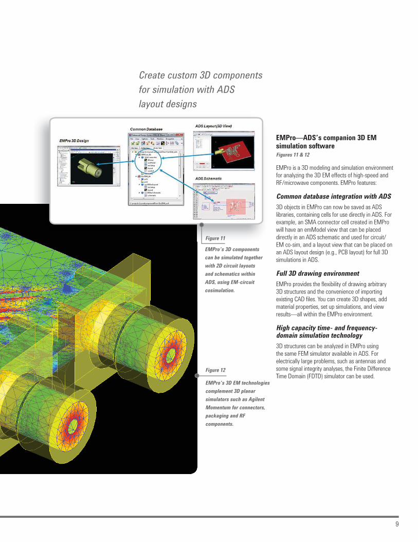
Create custom 3D components
for simulation with ADS
layout designs
EMPro—ADS’s companion 3D EM simulation softwareFigures 11 & 12
EMPro is a 3D modeling and simulation environment for analyzing the 3D EM effects of high-speed and RF/microwave components. EMPro features:
Common database integration with ADS
3D objects in EMPro can now be saved as ADS libraries, containing cells for use directly in ADS. For example, an SMA connector cell created in EMPro will have an emModel view that can be placed directly in an ADS schematic and used for circuit/EM co-sim, and a layout view that can be placed on an ADS layout design (e.g., PCB layout) for full 3D simulations in ADS.
Full 3D drawing environment
EMPro provides the flexibility of drawing arbitrary 3D structures and the convenience of importing existing CAD files. You can create 3D shapes, add material properties, set up simulations, and view results—all within the EMPro environment.
High capacity time- and frequency-domain simulation technology
3D structures can be analyzed in EMPro using the same FEM simulator available in ADS. For electrically large problems, such as antennas and some signal integrity analyses, the Finite Difference Time Domain (FDTD) simulator can be used.
EMPro’s 3D EM technologies
complement 3D planar
simulators such as Agilent
Momentum for connectors,
packaging and RF
components.
EMPro’s 3D components
can be simulated together
with 2D circuit layouts
and schematics within
ADS, using EM-circuit
cosimulation.
Figure 11
Figure 12

10
ADSM O S T C O M P L E T E S O L U T I O N
Industry-leading tools
for your high-frequency and
high-speed applications
RF & Microwave Design Flows
Agilent’s RF and microwave design and simulation tools provide the most complete solution for creating robust designs with first-pass success and high yields. ADS provides accurate models and powerful simulation technologies for circuit- to system-level designs. Seamlessly integrated circuit and EM simulation tools flow from schematic entry to production and verification. A complete set of the most accurate wireless verification tools in ADS provides true circuit verification to all wireless standards.
ADS offers designers the best
solutions and methodologies for
confidently designing RF modules.
RFIC/MMIC Design Figure 13
ADS provides the most complete set of advanced simulation tools, seamlessly integrated into a single environment, that flows from schematic entry to tape-out and packaging. These tools enable you to verify, prior to fabrication, that your RFIC/MMIC meets all specifications in its final package.
All major MMIC foundries offer complete front-to-back ADS PDKs, and also a broad range of SiGe/BiCMOS and CMOS-SOI PDKs are available.
RF Module DesignFigure 14
As the market and technology leader in RF module design solutions, Agilent EEsof EDA offers the best co-design platform and methodologies for designing RF modules with high confidence. ADS offers designers the best way to reduce risks of design failure due to unexpected parasitics.
Figure 14
Figure 13
ADS offers a complete set of
advanced simulation tools,
seamlessly integrated into one
single environment, which flows from
schematic entry to production and
packaging of the MMIC.

11
Accelerate your design with the
industry’s most complete set of
simulation tools and model libraries
High-Speed Digital Design Figure 15
ADS offers two bundles that put applicable simulators, libraries and capabilities into the hands of high-speed digital engineers. SystemVue generates IC models compliant to the IBIS-AMI standard. ADS provides the most complete data link analysis for standards like PCI Express®, Ethernet, DDR, HDMI, and USB. It enables complete chip-to-chip link analysis by co-simulating individual components, each at its most appropriate level of abstraction (link, circuit, layout, or geometry). S-parameter models, based on frequency-domain measurements, can be accurately imported into time-domain circuit and channel simulations, avoiding causality and passivity issues. Ultra-low BER contours can be generated in seconds, not days, resulting in dramatically reduced product design cycles.
RF Board Design
ADS provides proven board design solutions with very accurate models and simulation technologies covering circuit, EM and system level designs. It offers the widest variety of synthesis capabilities to explore alternatives quickly and balance RF performance, parts count and board area, within seconds, while also helping designers assess the cost-effectiveness of making versus buying a commercial component.
Accurate model libraries in ADS support different simulation domains for various applications. Behavioral models (important for initial system-level designs) can be extracted from datasheets, measurement or simulation. ADS’s robust layout artwork translators ensure a smooth hand-off to PCB manufacturing for RF board designers.
The ADS Eye Probe diagram allows you to
calculate parameters using algorithms drawn
from those on Agilent instruments.
AnalogDevices
Avago
AVX
Banpil
CEL
Coilcraft
Cyntec
DT Micro
DuPont
Freescale
Hittite
Johanson
KOA Speer
Metelics
Mini-Circuits
Mitsubishi
Modelithics
Motorola
Murata
NEC
Panasonic
Polyfet
Samsung
Samtec
Samyoung
Siemens
Taiyo Yuden
TDK
Temwell
TFT
TI
Toshiba
Agilent EEsof EDA actively engages
with component manufacturers to
create model libraries that provide
access the latest models and
technologies, including:
For an updated list, refer to:
www.agilent.com/find/eesof-vendor-
libraries
Figure 15
Time, psec
Mas
kD
ensi
ty
0
0.6
0.4
0.2
0.0
-0.2
-0.4
-0.6
50 100 150 200 250 300 350 400

12
ADSI N T E G R A T E D S O L U T I O N S
Achieve enterprise-wide
integration with your
design process
Easy links to instrumentation reduce design time and riskFigure 16
The integration of ADS with Agilent test instrumentation enables the seamless sharing of signals, measurements, algorithms, and data between the virtual software and physical hardware domains. Designers use this linkage to simulate and evaluate design trade-offs and what-ifs, and then turn the simulated signal into an RF test signal on the bench for hardware test. Conversely, designers can take the measured output signal from the device-under-test and bring it into ADS for additional analysis in the simulation environment.
Design Flow integration—partners for complete success
Agilent EEsof EDA aligns with key EDA vendors and frameworks to provide enhanced solutions that complement your investment. The open and flexible ADS environment ensures that a wide range of design flows are supported. ADS supports design flows based on a Cadence, Mentor or Zuken flow, for example, using industry-standard formats. Our expanding list of partners goes well beyond standard relationships and is part of an ongoing effort to provide best-in-class tools and technology that work in an integrated environment.
Use the 89600 VSA software to directly compare
simulations in ADS to measured results using
identical algorithms and assumptions.
Figure 16

13
X - P A R A M E T E R S
Accurate
nonlinear
models
Enable rapid design optimization
In high-frequency and high-speed designs, X-parameters overcome the system-level inaccuracies that often occur when using overly simplified behavioral models to simulate complex, nonlinear circuits. The use of X-parameters produces highly accurate nonlinear models—from either measurements or simulations—that can be passed through the design chain for quick and accurate simulation and optimization of system-level performance.
X-parameters:
• Are applicable to both large-signal and small-signal conditions, and for linear and nonlinear components
• Characterize—at all ports—the amplitude and relative phase of harmonics generated by components under large input power levels
• Correctly characterize impedance mismatches and frequency-mixing behavior to allow accurate simulation of cascaded nonlinear X-parameter blocks such as amplifiers and mixers

14
ADSW O R L D - C L A S S S U P P O R T
Accelerate success with convenient
product bundling plus comprehensive
support and training services
World-class support
Agilent Technologies is committed to customer satisfaction. We are dedicated to providing the right software, support and consulting solutions to increase your engineering productivity and advance your long-term success. Whether a novice or experienced user, Agilent’s customer support offerings can help you every step of the way. They include software and user manual updates via download or on CD-ROM, worldwide technical support via telephone, fax, e-mail, and the worldwide web. Agilent also offers dedicated support engineers in many countries to provide you with local language support. Phone support is available Monday through Friday, worldwide.
.
Training
Agilent EEsof EDA offers a full range of classroom courses, as well as live and self-paced e-learning courses, that provide instruction on the use of EDA software in a wide variety of applications. Live classes are conducted by experienced design engineers and focus on in-depth software operation and design examples. They also cover introductory and advanced microwave, RF, system and signal integrity design techniques. Self-paced e-learning courses allow you to set your own timetable. If travelling to a regularly scheduled class is problematic, or you have a group of designers that might benefit from a common class, your field sales representative can arrange an on-site class.
Knowledge Center
The Agilent EEsof Knowledge Center is an around-the-clock resource for designers. It contains thousands of support documents and hundreds of downloadable examples created by support engineers to supplement the ADS application examples and documentation. Maintenance Service Releases—with updates to previously released software versions—are also available for download. A tracking feature allows you to submit and manage your support cases and related defect and enhancement requests.

15
Purchase what you need today;
add greater functionality
as your needs evolve
ADS Environment + Elements
Configure a flexible ADS package that’s right for you. Choose an ADS Environment plus any combination of the following individual Element building blocks.
ADS can be ordered in value-priced bundles for simplicity and convenience, or in Environment + Element building blocks for greater flexibility.
ADS Core Environment
W2200 ADS CoreW2201 ADS Core + Layout
EM Simulation Elements
W2341 Momentum G2W2343 Momentum TurboW2342 FEM Simulator
Circuit & System Simulation Elements
W2300 Harmonic BalanceW2301 Circuit EnvelopeW2302 Transient/ConvolutionW2306 Linear Simulator ElementW2312 Transient Distributed Computing 8-packW2324 High Capacity Layout Pre-processorW2349 Electro-Thermal SimulatorW2500 Transient/Convolution GT
W2361 Agilent PtolemyW2362 RF Architect & SynthesisModel & Library ElementsW2304 Verilog-AMS CompilerW2305 X-Parameter GeneratorW2363 Mature Wireless LibraryW2364 2G/3G Wireless LibraryW2365 Wireless Networking LibraryW2366 Integrated Wireless LibraryW2367 WiMedia Wireless LibraryW2368 3GPP-LTE Wireless LibraryW2369 WVAN Wireless LibraryW2371 Asia DTV Wireless Library
Additional Recommended Products
W2401 EMPro Core EnvironmentW2402 EMPro Core + FEM
ADS product structure and options summary
1 2 3 4 5 6 7 8 9 10

For more information on Agilent Technologies’ products, applications or services, please contact your local Agilent office.
The complete list is available at:
www.agilent.com/find/contactus
AmericasCanada (877) 894 4414 Brazil (11) 4197 3600Mexico 01800 5064 800 United States (800) 829 4444
Asia PacificAustralia 1 800 629 485China 800 810 0189Hong Kong 800 938 693India 1 800 112 929Japan 0120 (421) 345Korea 080 769 0800Malaysia 1 800 888 848Singapore 1 800 375 8100Taiwan 0800 047 866Other AP Countries (65) 375 8100
Europe & Middle EastBelgium 32 (0) 2 404 93 40 Denmark 45 45 80 12 15Finland 358 (0) 10 855 2100France 0825 010 700* *0.125 €/minute
Germany 49 (0) 7031 464 6333 Ireland 1890 924 204Israel 972-3-9288-504/544Italy 39 02 92 60 8484Netherlands 31 (0) 20 547 2111Spain 34 (91) 631 3300Sweden 0200-88 22 55United Kingdom 44 (0) 118 927 6201
For other unlisted countries: www.agilent.com/find/contactus(BP-3-1-13)
Product specifications and descriptions in this
document subject to change without notice.
© Agilent Technologies, Inc. 2013
Published in USA, March 4, 2013
5988-3326EN
www.agilent.com
X-parameters is a trademark and registered trademark of Agilent Technologies in the US, EU, JP, and elsewhere. The X-parameters format and underlying equations are open and documented. For more information, visitwww.agilent.com/find/eesof-x-parameters-info
PCI-SIG®, PCIe® and the PCI Express® are US registered trademarks and/or service marks of PCI-SIG.
www.agilent.com/find/ads