6.3 graphics processor - · pdf filefifo geodelink™ interface unit ... 32-bpp 8, 16,...
TRANSCRIPT

AMD Geode™ LX Processors Data Book 237
Graphics Processor 33234H
6.3 Graphics ProcessorThe Graphics Processor is based on the graphics proces-sor used in the AMD Geode™ GX processor with severalfeatures added to enhance performance and functionality.Like its predecessor, the AMD Geode LX processor’sGraphics Processor is a BitBLT/vector engine that supportspattern generation, source expansion, pattern/sourcetransparency, 256 ternary raster operations, alpha blendersto support alpha-BLTs, incorporated BLT FIFOs, aGeodeLink™ interface and the ability to throttle BLTsaccording to video timing. Features added to the GraphicsProcessor include:
• Command buffer interface
• Hardware accelerated rotation BLTs
• Color depth conversion
• Palletized color
• Full 8x8 color pattern buffer
• Channel 3 - third DMA channel
• Monochrome inversion
The block diagram of the AMD Geode LX processor’sGraphics Processor is shown in Figure 6-10. Table 6-7 onpage 238 presents a comparison between the GraphicsProcessor features of the AMD Geode GX and LX proces-sors.
Figure 6-10. Graphics Processor Block Diagram
PatternRegisters
PatternExpansion
RasterSourceAligner &
ExpansionOperation
Source &DestinationRead FIFOs
AlphaBlendUnit
WriteAccumulation
FIFO
GeodeLink™ Interface Unit 0(GLIU0)
Channel 3Data Flow
Control
Channel 3Data
Formatter
2K FIFOand
LUT andPatternMemory
Channel 3Fetch
Engine
CommandBuffer Control
Logic andRegisters

238 AMD Geode™ LX Processors Data Book
Graphics Processor33234H
Table 6-7. Graphics Processor Feature Comparison
Feature AMD Geode™ GX Processor AMD Geode™ LX Processor
Color Depth 8, 16, 32-bpp 8, 16, 32-bpp (A) RGB 4 and 8-bit indexed
ROPs 256 (src, dest, pattern) 256 (2-src, dest and pattern)
BLT Buffers FIFOs in Graphics Processor FIFOs in Graphics Processor
BLT Splitting Managed by hardware Managed by hardware
Video Synchronized BLT/Vector Throttle by VBLANK Throttle by VBLANK
Bresenham Lines Yes Yes
Patterned (stippled) Lines No Yes
Screen to Screen BLT Yes Yes
Screen to Screen BLT with mono expansion
Yes Yes
Memory to Screen BLT Yes (through CPU writes) Yes (throttled rep movs writes)
Accelerated Text No No
Pattern Size (Mono) 8x8 pixels 8x8 pixels
Pattern Size (Color) 8x1 (32 pixels) 8x8 pixels
8x2 (16 pixels)
8x4 (8 pixels)
Monochrome Pattern Yes Yes (with inversion)
Dithered Pattern (4 color) No No
Color Pattern 8, 16, 32-bpp 8, 16, 32-bpp
Transparent Pattern Monochrome Monochrome
Solid Fill Yes Yes
Pattern Fill Yes Yes
Transparent Source Monochrome Monochrome
Color Key Source Transparency Y with mask Y with mask
Variable Source Stride Yes Yes
Variable Destination Stride Yes Yes
Destination Write Bursting Yes Yes
Selectable BLT Direction Vertical and Horizontal Vertical and Horizontal
Alpha BLT Yes (constant α or α/pix) Yes (constant α, α/pix, or sep. α channel)
VGA Support Decodes VGA Register Decodes VGA Register
Pipeline Depth 2 ops Unlimited
Accelerated Rotation BLT No 8, 16, 32-bpp
Color Depth Conversion No 5:6:5, 1:5:5:5, 4:4:4:4, 8:8:8:8
AMD Geode™ LX Processors Data Book 239
Graphics Processor 33234H
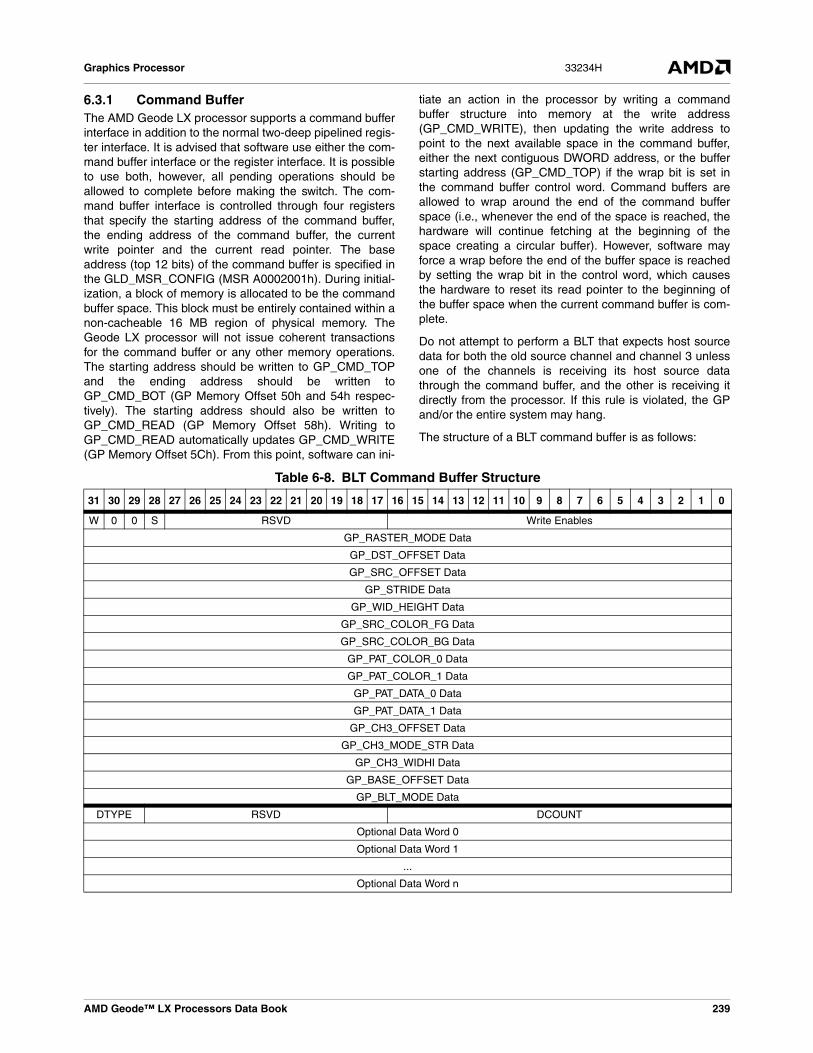
6.3.1 Command BufferThe AMD Geode LX processor supports a command bufferinterface in addition to the normal two-deep pipelined regis-ter interface. It is advised that software use either the com-mand buffer interface or the register interface. It is possibleto use both, however, all pending operations should beallowed to complete before making the switch. The com-mand buffer interface is controlled through four registersthat specify the starting address of the command buffer,the ending address of the command buffer, the currentwrite pointer and the current read pointer. The baseaddress (top 12 bits) of the command buffer is specified inthe GLD_MSR_CONFIG (MSR A0002001h). During initial-ization, a block of memory is allocated to be the commandbuffer space. This block must be entirely contained within anon-cacheable 16 MB region of physical memory. TheGeode LX processor will not issue coherent transactionsfor the command buffer or any other memory operations.The starting address should be written to GP_CMD_TOPand the ending address should be written toGP_CMD_BOT (GP Memory Offset 50h and 54h respec-tively). The starting address should also be written toGP_CMD_READ (GP Memory Offset 58h). Writing toGP_CMD_READ automatically updates GP_CMD_WRITE(GP Memory Offset 5Ch). From this point, software can ini-
tiate an action in the processor by writing a commandbuffer structure into memory at the write address(GP_CMD_WRITE), then updating the write address topoint to the next available space in the command buffer,either the next contiguous DWORD address, or the bufferstarting address (GP_CMD_TOP) if the wrap bit is set inthe command buffer control word. Command buffers areallowed to wrap around the end of the command bufferspace (i.e., whenever the end of the space is reached, thehardware will continue fetching at the beginning of thespace creating a circular buffer). However, software mayforce a wrap before the end of the buffer space is reachedby setting the wrap bit in the control word, which causesthe hardware to reset its read pointer to the beginning ofthe buffer space when the current command buffer is com-plete.
Do not attempt to perform a BLT that expects host sourcedata for both the old source channel and channel 3 unlessone of the channels is receiving its host source datathrough the command buffer, and the other is receiving itdirectly from the processor. If this rule is violated, the GPand/or the entire system may hang.
The structure of a BLT command buffer is as follows:
Table 6-8. BLT Command Buffer Structure
31 30 29 28 27 26 25 24 23 22 21 20 19 18 17 16 15 14 13 12 11 10 9 8 7 6 5 4 3 2 1 0
W 0 0 S RSVD Write Enables
GP_RASTER_MODE Data
GP_DST_OFFSET Data
GP_SRC_OFFSET Data
GP_STRIDE Data
GP_WID_HEIGHT Data
GP_SRC_COLOR_FG Data
GP_SRC_COLOR_BG Data
GP_PAT_COLOR_0 Data
GP_PAT_COLOR_1 Data
GP_PAT_DATA_0 Data
GP_PAT_DATA_1 Data
GP_CH3_OFFSET Data
GP_CH3_MODE_STR Data
GP_CH3_WIDHI Data
GP_BASE_OFFSET Data
GP_BLT_MODE Data
DTYPE RSVD DCOUNT
Optional Data Word 0
Optional Data Word 1
...
Optional Data Word n

240 AMD Geode™ LX Processors Data Book
Graphics Processor33234H
Table 6-9. Vector Command Buffer Structure
31 30 29 28 27 26 25 24 23 22 21 20 19 18 17 16 15 14 13 12 11 10 9 8 7 6 5 4 3 2 1 0
W 0 1 S RSVD Write Enables
GP_RASTER_MODE Data
GP_DST_OFFSET Data
GP_VEC_ERR Data
GP_STRIDE Data
GP_VEC_LEN Data
GP_SRC_COLOR_FG Data
GP_PAT_COLOR_0 Data
GP_PAT_COLOR_1 Data
GP_PAT_DATA_0 Data
GP_PAT_DATA_1 Data
GP_CH3_MODE_STR Data
GP_BASE_OFFSET Data
GP_VECTOR_MODE Data
Table 6-10. LUT (Lookup Table) Load Command Buffer Structure
31 30 29 28 27 26 25 24 23 22 21 20 19 18 17 16 15 14 13 12 11 10 9 8 7 6 5 4 3 2 1 0
W 1 0 S RSVD WE
GP_LUT_INDEX Data
DTYPE RSVD DCOUNT
Optional Data Word 0
Optional Data Word 1
...
Optional Data Word n
Table 6-11. Data Only Command Buffer Structure
31 30 29 28 27 26 25 24 23 22 21 20 19 18 17 16 15 14 13 12 11 10 9 8 7 6 5 4 3 2 1 0
W 1 1 0 RSVD 1
DTYPE RSVD DCOUNT
Optional Data Word 0
Optional Data Word 1
...
Optional Data Word n

AMD Geode™ LX Processors Data Book 241
Graphics Processor 33234H
Where:
6.3.2 Channel 3Channel 3 is an additional DMA channel (in addition to thefirst two channels: source and destination) that can fetchdata from memory or receive it through host source writes.This channel has all of the data conversion features built into perform rotational BLTs, color depth conversions, pallet-ized color support (LUT lookups), 8x8 color pattern, andpatterned vector support. The data coming out of this DMApipeline can selectively be steered into the old sourcechannel or the old pattern channel, whichever is more nat-ural for a given ROP. Note that not all data coming out ofthis pipeline can be arbitrarily ROPed with other data (i.e.,rotational BLT data can not be ROPed with any other chan-nel, alpha data is expected to be used as input to the alphaunit). The behavior of channel 3 is controlled throughGP_CH3_MODE_STR (GP Memory Offset 64h). Channel3 is also set up to be mostly independent from the othertwo channels, so it calculates its own addresses and pixelcounters based on the GP_CH3_OFFSET andGP_CH3_WIDHI (GP Memory Offset 60h and 68h respec-tively). It is possible to set up this channel with a differentwidth and height than the destination (i.e., a rotation BLTwill have width and height swapped from the destination).As long as the number of pixels to be fetched is the sameas the output, there should be no problem. If this channelhas too few pixels to complete the BLT and is not in hostsource mode, the BLT will terminate when this channel hasfetched all of the requested data, and the underflow bit willbe set in GP_BLT_STATUS (GP Memory Offset 44h). Ifthis channel has pixels left when the BLT is complete, theextra pixels are discarded and the overflow bit is set inGP_BLT_STATUS.
Channel 3 has the ability to begin prefetching data for apending BLT before the active BLT has completed. The PEbit in the GP_CH3_MODE_STR register (GP Memory Off-set 64h[19]) can be set to allow prefetching for that BLT.Prefetching can safely be set for any BLT that does notrequire write data from the previous BLT as read data onchannel 3. The GP does no hazard checking to verify thesafety of the prefetch. This feature will incrementallyimprove performance as it allows the GP to make use ofbus bandwidth that would otherwise have gone unused.Prefetching has the lowest bus priority and is only doneopportunistically.
The X and Y bits (bits 29 and 28) in theGP_CH3_MODE_STR register do not need to be pro-grammed the same as the bits in the GP_BLT_MODE reg-ister (GP Memory Offset 40h). If they are the same, theresult is a source copy. If both bits are programmed oppo-site from the GP_BLT_MODE register, then the result is a180° rotation. If only one bit is opposite, the result is a flip inthat direction.
When the current operation is a vector, channel 3 can gen-erate byte enables to stylize the vector based upon the pro-grammed pattern. Channel 3 cannot be used to generateany pixel data while rendering vectors.
Table 6-12. Bit Descriptions
Name Description
WE Write Enable. One bit for each of the required DWORDs which follow in the command buffer. A set bit indicates that the field is valid and should be updated in the GP. A clear bit indicates the field should be skipped.
W Wrap Bit. If set, then return to the top of command buffer space after executing this buffer.
S Stall Bit. Execution of this command will be stalled until the GP’s pipeline is empty.
DTYPE Data Type. Type of data that follows:
000: Host source data to old host source channel
001: Host source data to new channel 3
010: Pattern data to GP_PAT_COLOR_2 - GP_PAT_COLOR5 (GP Memory Offset 20h-2Ch)
011: Write data for LUT/color pattern space
1xx: Reserved
DCOUNT DWORD Count. Number of DWORDs of data that follow.

242 AMD Geode™ LX Processors Data Book
Graphics Processor33234H
6.3.2.1 Rotating BLTsThis feature of the GP allows bitmaps to be rotated 90°,180° or 270°. The 90° and 270° modes work by readingvertical strips of the source bitmap that are one cache line(32 bytes) wide starting at either the top right or bottom leftcorner of the bitmap. The output is written as tiles that areone cache line wide by either 8, 16 or 32 pixels tall,depending on the color depth of the input data stream.Because the data is not written out in scan line order, noneof the other channels can be correctly ROPed with thedata, so this operation should be treated as a source copy.Also, because the entire buffer memory will be used for thefetched data, the input data stream may not be indexedcolor (it may be declared as 8-bpp, but it will not be con-verted through LUT lookups. This may be done on a sec-ond pass after the rotation).
To program a rotation BLT of 90° clockwise, the rotation bitshould be on in the GP_CH3_MODE_STR register (GPMemory Offset 64h[23]), the X and Y bits for channel 3should be clear and set respectively, the X and Y in theGP_BLT_MODE register (GP Memory Offset 40h[9:8])should both be clear, GP_CH3_OFFSET (GP Memory Off-set 60h) should point to the bottom left corner of the sourceand GP_DST_OFFSET (GP Memory Offset 00h) shouldpoint to the top left corner of the destination.
To program a rotation BLT of 270° clockwise, the rotationbit should be on in the GP_CH3_MODE_STR register, theX and Y bits for channel 3 should be set and clear respec-tively, the X and Y in the GP_BLT_MODE register shouldboth be clear, GP_CH3_OFFSET should point to the topright corner of the source and GP_DEST_OFFSET shouldpoint to the top left corner of the destination.
To program a rotation BLT of 180° clockwise, the rotationbit should be off in the GP_CH3_MODE_STR register, theX and Y bits for channel 3 should be opposite their counter-parts in the GP_BLT_MODE register, andGP_CH3_OFFSET should point to the opposite cornerfrom GP_DEST_OFFSET.
For all rotations, it is required that both the source strideand the destination stride be aligned to a cache line bound-ary (i.e., bottom 5 bits of stride are all 0s). Do not attempt torotate host source data. The fill algorithm would be toocomplex and the likelihood of causing a FIFO underrun andhanging the GP is too high.
Note that for rotation BLTs, the PL bit in theGP_CH3_MODE_STR register (GP Memory Offset64h[20]) may not be set. The entire buffer is needed for therotation so the LUT and pattern data may not be retained.
6.3.2.2 Rotating VideoThe GP is primarily an RGB engine that does not nativelyunderstand YUV data. However, it is possible to performvideo rotations using the GP hardware assuming the datais formatted correctly. If the data is in 4:2:0 format with theY data separated from the UV data, the rotation can beperformed by passing each channel of the image sepa-rately through the GP and setting the color depth appropri-ately. For the Y data, the color depth should be set to 8-bpp3:3:2. The same is true for the U and V data if they are inseparate channels. If the U and V data are combined inone buffer then the color depth should be set to 16-bpp5:6:5. Similarly, 4:4:4 format data can also be supported ifeach channel is stored in its own buffer.
6.3.2.3 Color Depth ConversionIf the BPP/FMT bits in the GP_CH3_MODE_STR register(GP Memory Offset 64h]27:24]) are set different than theBPP/FMT bits in the GP_RASTER_MODE register (GPMemory Offset 38h[31:28]), then the incoming data is con-verted to match the output format. If the BGR bit (GP Mem-ory Offset 64h[22]) is set, then the red and blue channels ofthe data will be swapped prior to the depth conversion (ifany).
A 24-bpp source format is supported on channel 3 allowingpacked RGB pixels to be unpacked as they are written intothe frame buffer. For this format, the channel 3 width isspecified in DWORDs, not pixels. As a result, the channel 3offset for 24-bpp data must therefore be aligned to aDWORD boundary. BGR conversion is not possible in thisformat since this operation is done before the depth con-version. 24-bpp images may not be rotated, they wouldneed to be converted into another format first.

AMD Geode™ LX Processors Data Book 243
Graphics Processor 33234H
6.3.2.4 Palletized Color SupportIf the Preserve LUT Data bit is set in theGP_CH3_MODE_STR register (GP Memory Offset64h[20]) then 1K of the 2K buffer space will be allocated tobe a LUT. As long as this bit remains set, the LUT data ispreserved as written. Setting this bit has the impact ofslightly lowering performance since it limits the prefetchability of the GP, or its ability to receive massive amountsof host source data. This is unlikely to be a significantissue, but if the LUT is not needed for future BLTs, thenclearing this bit is recommended. It is required to becleared during rotations since the entire 2K buffer space isneeded.
If the BPP/FMT bits in the GP_CH3_MOD_STR register(GP Memory Offset 64h[27:24]) indicate that the incomingdata is either 4 or 8-bpp indexed mode, then the LUT willbe used to convert the data into 16 or 32-bpp mode asspecified in the GP_RASTER_MODE register’s BPP/FMTfield (GP Memory Offset 38h[31:28]). The LUT should beloaded prior to initiating such a BLT by writing an addressto the GP_LUT_INDEX register (GP Memory Offset 70h)followed by one or more DWORD writes to theGP_LUT_DATA register (GP Memory Offset 74h) that willbe loaded into the LUT starting at that address. The
address automatically increments with every write.Addresses 00h-FFh are used for 8-bpp indexed pixels andaddresses 00h-0Fh are used for 4-bpp indexed pixels. Theresult of a lookup is always a DWORD. If the output formatis only 16-bpp, then only the data in the two least signifi-cant bytes is used.
For 4-bpp incoming data, two pixels are packed within abyte such that bits[7:4] contain the leftmost pixel andbits[3:0] contain the rightmost pixel. The pixel ordering for4-bit pixels is shown in Table 6-13.
For host source data, the starting offset into the firstDWORD is taken from GP_CH3_OFFSET[1:0] (andGP_CH3_OFFSET[28] if the data is 4-bpp). For data beingfetched from memory, GP_CH3_OFFSET[23:0] specifiesthe starting byte and GP_CH3_OFFSET[28] specifies thenibble within the byte for 4-bpp mode.
Note that, regardless of the output pixel depth, palletizedcolor has a throughput of no more than one clock per pixel.The LUTs share memory with the incoming data FIFO, sothe datapath first pops the incoming indexed pixels out ofthe FIFO (8 or 16 at a time), then performs the LUT lookup,one pixel per clock, for the next 8 or 16 clocks, then mustpop more data out of the FIFO.
Table 6-13. Pixel Ordering for 4-Bit Pixels
31 30 29 28 27 26 25 24 23 22 21 20 19 18 17 16 15 14 13 12 11 10 9 8 7 6 5 4 3 2 1 0
Pixel 6 Pixel 7 Pixel 4 Pixel 5 Pixel 2 Pixel 3 Pixel 0 Pixel 1

244 AMD Geode™ LX Processors Data Book
Graphics Processor33234H
6.3.2.5 Anti-Aliased Text SupportChannel 3 can be setup to fetch 4-bpp alpha channel datathat can be combined with either 16 or 32-bpp color ormonochrome source data using the alpha unit in the GP.The depth and type in the GP_CH3_MODE_STR registershould be setup to indicate 4-bpp alpha and the AS bits inthe GP_RASTER_MODE register (GP Memory Offset38h[19:17]) should be set to 110 to select the alpha fromchannel 3.
6.3.2.6 8x8 Color PatternChannel 3 can also be configured to source full color pat-terns into the GP. The pattern data is stored in the 2Kbuffer using writes to the GP_LUT_INDEX andGP_LUT_DATA registers (GP Memory Offset 70h and74h, respectively) as done for loading the LUT. Addresses100h-10Fh are used for 8-bpp patterns, 100h-11Fh areused for 16-bpp patterns and 100h-13Fh are used for 32-bpp patterns. Note that this data will not be persistent in thebuffer. If channel 3 is later used in non-pattern mode, thenthe pattern data will no longer be present in the buffer.Therefore it is usually necessary to reload the pattern databefore any BLT requiring 8x8 color pattern support. Thedepth of the pattern is determined by the BPP/FMT bits(GP Memory Offset 64h[27:24]) of theGP_CH3_MODE_STR register (4-bpp is not allowed in
pattern mode). The output of the pattern hardware is con-verted to the depth specified in the BPP/FMT GP bits(Memory Offset 38h[31:28]) of the GP_RASTER_MODEregister if the two depths do not match.
6.3.2.7 Patterned VectorsWhen pattern mode is enabled during a vector operation,channel 3 generates a patterned (stippled) vector. This is alinear monochrome pattern that is stored in the LUT atlocations 100h and 101h. The first DWORD (100h) con-tains the pattern, which is a string of four to 32 bits startingat bit 0. The second DWORD is used to indicate the lengthof the pattern and is a string of four to 32 ones starting atbit 0. Tables 6-14 and 6-15 show an example vector patternand length. The result of this vector pattern/length would bea 14-bit long pattern that, when repeated, looks Figure 6-11.
The dark pixels are rendered using the selected ROP,while the light pixels are transparent. The ROP may con-tain any combination of source, destination and pattern. Ifpattern is enabled in the ROP, it comes from the old (non-channel 3) pattern hardware. Note that a vector patternmust be at least four pixels long. For shorter patterns (i.e.,two on, one off), repeat the pattern in the pattern registersuntil it is at least four pixels long.
Figure 6-11. 14-Bit Repeated Pattern
Table 6-14. Example Vector Pattern
31 30 29 28 27 26 25 24 23 22 21 20 19 18 17 16 15 14 13 12 11 10 9 8 7 6 5 4 3 2 1 0
0 0 0 0 0 0 0 0 0 0 0 0 0 0 0 0 0 0 0 0 1 1 0 0 1 1 0 0 1 1 1 1
Table 6-15. Example Vector Length
31 30 29 28 27 26 25 24 23 22 21 20 19 18 17 16 15 14 13 12 11 10 9 8 7 6 5 4 3 2 1 0
0 0 0 0 0 0 0 0 0 0 0 0 0 0 0 0 0 0 1 1 1 1 1 1 1 1 1 1 1 1 1 1

AMD Geode™ LX Processors Data Book 245
Graphics Processor 33234H
6.3.2.8 Channel 3 Host SourceChannel 3 also supports host source data writes. When theHS bit is set in the GP_CH3_MODE_STR register (GPMemory Offset 64h[18]), the channel 3 fetch engine is dis-abled and the FIFOs are filled via register writes to theGP_CH3_HSRC register (GP Memory Offset 6Ch) or itsaliased space. If the PL bit in the GP_CH3_MODE_STRregister (GP Memory Offset 64h[20]) is not set then the GPcan accept 2 KB of data through host source writes beforeits buffers are full. However, since monochrome is not sup-ported on this channel, the output flow rate of data closelymatches the input flow (worst case is 8:1 if output is 32-bppand input is 4-bpp) so it is unlikely that the GP will ever fillup. If it does fill its 2K buffer, then writes from the GLIU willbe disabled until there is space available to store it. Soft-ware should not have to poll this interface to keep fromoverrunning the FIFOs. It should be noted that, while it ispossible to program the GP to accept host source data onboth the source channel and channel 3, this should not bedone unless one of the channels is filled through the com-mand buffer and the other through direct writes to the reg-ister. If this is the case, it is recommended that the sourcechannel be filled through the command buffer and channel3 be filled through register writes, since this will eliminatepolling and provide higher performance. It will probablyrequire less memory as well since the data into the sourcechannel will likely be monochrome and fit into a smallercommand buffer.
6.3.2.9 Channel 3 HintsSoftware should try to setup the BLTs to use channel 3whenever possible. This channel is designed to have thehighest performance, since it is capable of prefetchinggreat quantities of data even before a BLT actually starts.This channel must be used when performing rotating BLTs,color depth conversions, palletized color, or 8x8 color pat-terns. This channel can carry source data, destination data,per-pixel alpha data, or pattern data. This channel cannotbe used for monochrome data, and cannot be used forsource or destination data if it must be ROPed with 8x8pattern data. If the pattern does not need to be 8x8, thenthe old pattern hardware should be used as this will free upchannel 3 to be used for higher performance memoryfetches and host source data.
The source channel has the next highest performance, andshould be used if two channels are necessary or if the datacannot be carried on channel 3. This channel can be usedto fetch destination data, and the performance will behigher than using the destination channel.
The destination channel should only be used to carry desti-nation data when it cannot be carried on either of the othertwo channels. This should only be the case when the ROPcalls for source, destination and pattern, when the opera-tion is a vector, or when alpha requires an A and B chan-nel. In all other cases, performance will be higher ifdestination is fetched on either the source channel or chan-nel 3.
6.3.3 BLT OperationTo perform a BLT, several registers must first be config-ured by the driver to specify the operation of the BLTengine. These registers specify the source and destinationoffsets into the frame buffer, the width and height of theBLT rectangle, and the raster mode or alpha blend mode.In addition, any source colors, pattern colors, and patterndata should be loaded before initiating a BLT.
BLTs are initiated by writing to the GP_BLT_MODE regis-ter (GP Memory Offset 40h). This register indicates theneed for source and destination data, and defines the typeof source data, and the direction in which the BLT shouldproceed. Color BLTs may be performed from left to right orright to left, top to bottom or bottom to top. This allows datato be transferred within the screen space without corruptingthe areas from where the data is being copied. Whenmonochrome source is used, however, the BLT must beperformed from left to right.
Instead of BLT buffers (L1 cache), Source Read, Destina-tion Read, and Destination Write FIFOs are used to tempo-rarily store the data that flows through the GraphicsProcessor. Overflowing the FIFOs is not possible since thetransfer is managed by the hardware anywhere within the16 MB frame buffer memory region. At the start of a BLT,two cache lines of destination data and up to four cachelines of source data are fetched (if needed). Source data isfetched in groups of four cache lines, when possible.
Source data may either be read from within the framebuffer memory space or received from the CPU via writesto the GP_HST_SRC register (GP Memory Offset 48h). Ineither case, the data may be monochrome or color, asspecified in the GP_BLT_MODE register (GP Memory Off-set 40h). If no source color is specified, the contents of theGP_SRC_COLOR_FG register (GP Memory Offset 10h) isused as the default. For a solid fill, neither source, destina-tion, nor pattern are required and the resulting output pixelis derived from the contents of the GP_PAT_COLOR_0register (GP Memory Offset 18h). The destination of theBLT is always within the frame buffer memory region and isalways the specified color depth, never monochrome.
A bit is provided in the mode registers to allow BLTs andvectors to be throttled. When this bit is set for a particularoperation, that operation does not begin executing until thenext time the video timing enters vertical blank (VBLANK).This function can be used to improve 2D quality by mini-mizing tearing that occurs when writing to the frame bufferwhile the image is being drawn to the screen.
246 AMD Geode™ LX Processors Data Book
Graphics Processor33234H
6.3.4 Vector OperationGenerating a vector requires a similar setup to a BLT. Reg-isters must be written to specify the X and Y offsets of thestarting position of the vector within the frame buffer, thevector length, and the three error terms required by theBresenham algorithm. In addition, any pattern colors andpattern data should be loaded before initiating the vector.Source data is not fetched when rendering vectors.Instead, the contents of the GP_SRC_COLOR_FG register(GP Memory Offset 10h) are used as the constant color forthe vector.
Vectors are initiated by writing to the GP_VECTOR_MODE(GP Memory Offset 3Ch) register. This register also indi-cates the need for destination data, and defines the majoraxis (X or Y) and the major and minor directions (incre-menting or decrementing) of the vector.
As in the BLT operation, vectors can be throttled by videotiming to prevent tearing. Setting the TH bit in theGP_VECTOR_MODE register (GP Memory Offset 3Ch[4])causes the Graphics Processor to wait until the next timethat video timing enters VBLANK before beginning to ren-der the vector.
6.3.5 Pipelined OperationMost of the graphics registers are pipelined. When the reg-isters are programmed and the operation begins, the con-tents of the registers are moved from slave registers tomaster registers, leaving the slave registers available foranother operation. A second BLT or vector operation canthen be loaded into the slave registers while the first opera-tion is rendered. If a second BLT is pending in the slaveregisters, additional write operations to the graphics regis-ters will corrupt the register values of the pending BLT.Software must prevent this from happening by checkingthe Primitive Pending bit in the GP_BLT_STATUS register(GP Memory Offset 44h[2]).
The GP_PAT_COLOR_2 through GP_PAT_COLOR_5(GP Memory Offset 20h-2Ch) registers are not pipelined. Ifthey are used in a new graphics operation, they should notbe written when the Primitive Busy bit (GP Memory Offset44h[0]) is set and the Primitive Pending bit is not set in theGP_BLT_STATUS register, and the active operation isusing these registers. Writing to these registers when aBLT is active corrupts that operation.
6.3.6 Pattern GenerationThe Graphics Processor contains hardware support for 8x8monochrome patterns (expanded to two colors), and colorpatterns. Color patterns can be 8x4 in 8-bpp mode, 8x2 in16-bpp mode, and 8x1 in 32-bpp mode. Pattern alignmentis based on the destination X and Y LSBs of the pixel beingdrawn, so software can perform pattern justifications byadjusting these two parameters. For solid fill primitives, thepattern hardware is disabled and the pattern color isalways sourced from the GP_PAT_COLOR_0 register (GPMemory Offset 18h).
6.3.6.1 Monochrome PatternsMonochrome patterns are enabled by selecting mono-chrome pattern mode in the GP_RASTER_MODE register(GP Memory Offset 38h). Pixels that correspond to a clearbit in the pattern are rendered using the color specified inthe GP_PAT_COLOR_0 (GP Memory Offset 18h) register,and pixels that correspond to a set bit in the pattern arerendered using the color specified in theGP_PAT_COLOR_1 register (GP Memory Offset 1Ch).
If the pattern transparency bit is set in theGP_RASTER_MODE register (GP Memory Offset 38h),those pixels corresponding to a clear bit in the pattern dataare not drawn, leaving the frame buffer pixels at these loca-tions untouched.
The pattern itself is loaded into the GP_PAT_DATA_0 andGP_PAT_DATA_1 registers, with row 0 loaded intoGP_PAT_DATA_0 (GP Memory Offset 30h[7:0] (bit 7being the left-most pixel on the screen)), and row 7 loadedinto GP_PAT_DATA_1 (GP Memory Offset 34h[31:24], seeTable 6-16).
AMD Geode™ LX Processors Data Book 247
Graphics Processor 33234H
6.3.6.2 Color PatternsColor patterns are enabled by selecting the color patternmode in the GP_RASTER_MODE register (GP MemoryOffset 38h). In this mode, both of the GP_PAT_DATA reg-isters and all six of the GP_PAT_COLOR registers arecombined to provide a total of 256 bits of pattern. The num-ber of lines that the pattern can hold is dependent upon thenumber of bits per pixel. When performing a BLT thatneeds a deeper color pattern than is supported (such as8x8), software is responsible for breaking the BLT intoblocks such that the height of each block does not exceedthe depth of the pattern. After each block is completed,software must update the pattern registers before continu-ing with the next block of the BLT. As a result of having aprogrammable stride value, it is now possible to reduce thenumber of passes required to perform a BLT requiring acolor pattern, by multiplying the stride value by the numberof passes that are required to perform the BLT. For exam-ple, in 8-bpp mode, where only an 8x4 pattern fits, thestride value could be doubled such that all of the even lines
would be BLTed during the first pass, and all of the oddlines during the second pass. The pattern registers shouldbe programmed with the even lines on the first pass andthe odd lines on the second pass, and the Y Offset valueshould be the start of the bitmap on the first pass and thestart of the second line of the bitmap on the second pass.The algorithm can be extended to handle 8x2 and 8x1 pat-terns in four and eight passes. This only works, however,when the source and destination are non-overlapping.When performing an overlapping BLT, it is necessary to fallback to breaking the BLT into four, two, or one consecutivelines and reprogramming the pattern registers betweeneach block.
Pattern transparency is not supported in color patternmode.
In 8-bpp mode, there is a total of four lines of pattern, eachline with eight pixels as illustrated in Table 6-17 on page248.
Table 6-16. Example of Monochrome Pattern
Bit 7 Bit 6 Bit 5 Bit 4 Bit 3 Bit 2 Bit 1 Bit 0
GP_PAT_DATA_0[7:0] - 14h
GP_PAT_DATA_0[15:8] - 22h
GP_PAT_DATA_0[23:16] - 41h
GP_PAT_DATA_0[31:24] - 80h
GP_PAT_DATA_1[7:0] - 41h
GP_PAT_DATA_1[15:8] - 22h
GP_PAT_DATA_1[23:16] - 14h
GP_PAT_DATA_1[31:24] - 08h

248 AMD Geode™ LX Processors Data Book
Graphics Processor33234H
In 16-bpp mode, there is a total of two lines of pattern, each line with eight pixels as illustrated in Table 6-18. In 32-bppmode, there is only one line of pattern with eight pixels. The ordering of the registers in the line from left to right is as fol-lows:
1) GP_PAT_COLOR_5
2) GP_PAT_COLOR_4
3) GP_PAT_COLOR_3
4) GP_PAT_COLOR_2
5) GP_PAT_COLOR_1
6) GP_PAT_COLOR_0
7) GP_PAT_DATA_1
8) GP_PAT_DATA_0.
Table 6-17. Example of 8-Bit Color Pattern (3:3:2 Format)
Byte 7 Byte 6 Byte 5 Byte 4 Byte 3 Byte 2 Byte 1 Byte 0
GP_PAT_DATA_1 (02024002h)GP_PAT_DATA_0 (40024002h)
02 02 40 02 40 02 40 02
GP_PAT_COLOR_1 (0240E340h)GP_PAT_COLOR_0 (0240E340h)
02 40 E3 403 02 40 E3 40
GP_PAT_COLOR_3 (40E300E3h)GP_PAT_COLOR_2 (40E300E3h)
40 E3 00 E3 40 E3 00 E3
GP_PAT_COLOR_5 (0240E340h)GP_PAT_COLOR_4 (0240E340h)
02 40 E3 40 02 40 E3 40
Table 6-18. Example of 16-Bit Color Pattern (5:6:5 Format)
Byte 15:14
Byte 13:12
Byte 11:10
Byte 9:8
Byte 7:6
Byte 5:4
Byte 3:2
Byte 1:0
GP_PAT_COLOR_1 (00100010h)
GP_PAT_COLOR_0 (40000010h)
GP_PAT_DATA_1 (02028002h)
GP_PAT_DATA_0 (80028002h)
0010 0010 4000 0010 4000 0010 4000 0010
GP_PAT_COLOR_5 (00104000h)
GP_PAT_COLOR_4 (F81F4000h)
GP_PAT_COLOR_3 (0280E380h)
GP_PAT_COLOR_2 (0280E380h)
0010 4000 F81F 4000 0010 4000 F81F 4000

AMD Geode™ LX Processors Data Book 249
Graphics Processor 33234H
6.3.7 8x8 Color PatternsThe new channel 3 hardware provides the capability of per-forming BLTs with 64 pixel color patterns at all colordepths. To setup this mode, software first loads the patterndata into the LUT beginning at address 100h The least sig-nificant byte of this first DWORD contains the upper leftmost pixel of the pattern. For 8-bpp mode, the most signifi-cant byte of the next DWORD contains the upper rightmost pixel of the pattern. In 16-bpp mode, the upper rightmost pixel is contained in the most significant bytes of thefourth DWORD, and for 32-bpp mode, the eighth DWORDcontains the upper right most pixel. The next line of the pat-tern begins at the DWORD that follows the last pixel of theprevious line, such that the pattern is packed into the spacerequired to hold it. So for 8-bpp mode, the top left pixel is inthe least significant byte of the DWORD at address 100h inthe LUT, the top right pixel is in the most significant byte ofthe DWORD at address 101. The bottom left pixel is in theleast significant byte of the DWORD at address 10Eh andthe bottom right pixel is in the most significant byte of theDWORD at address 10Fh.
To enable this mode, the EN and PM bits should be set inthe GP_CH3_MODE_STR register (GP Memory Offset64h[31, 21]): EN, PM. The PS, HS, RO, X, and Y bitsshould not be set in the GP_CH3_MODE_STR register.The BPP/FMT bits in the GP_CH3_MODE_STR register(bits [27:24]) indicate the color depth of the pattern data. Ifthis does not match the BPP/FMT bits in the
GP_RASTER_MODE register (GP Memory Offset38h[31:28]), then the pattern is translated to the depthspecified by the GP_RASTER_MODE register.
6.3.8 Source DataWhen called for by the raster operation or alpha blender,software should set the source required bits in theGP_BLT_MODE register (GP Memory Offset 40h) so thatsource data is fetched from the frame buffer memory orcan be written by the host to the GP_HST_SRC register(GP Memory Offset 48h). Regardless of its origination,source data can either be monochrome (expanded to twocolors) or color. The hardware aligns the incoming sourcedata to the appropriate pixel lanes for writing to the destina-tion. Source data is only used when in BLT mode. In vectormode, GP_SRC_COLOR_FG (GP Memory Offset 10h) isforced onto the source channel.
6.3.8.1 Source Data FormatsThe Graphics Processor expects to see the left-most pixelson the screen in the least significant bytes of the DWORDand the right-most pixels in the most significant bytes. Formonochrome data within a byte, the left-most pixels are inthe most significant bits of the byte, and the right-most pix-els are in the least significant bits. These formats areshown more clearly in Table 6-19, Table 6-20, Table 6-21,and Table 6-22.
Table 6-19. 32-bpp 8:8:8:8 Color Data Format
Byte 3 Byte 2 Byte 1 Byte 0
Alpha/Unused Red Green Blue
Table 6-20. 16-bpp Color Data Format
Format
Byte 3 Byte 2 Byte 1 Byte 0
Right Pixel Data Left Pixel Data
5:6:5 Red Green Blue Red Green Blue
4:4:4:4 Alpha Red Green Blue Alpha Red Green Blue
1:5:5:5 A Red Green Blue A Red Green Blue
Table 6-21. 8-bpp 3:3:2 Color Data Format
Byte 3 Byte 2 Byte 1 Byte 0
Right Pixel Data (3:3:2) Pixel 2 Data Pixel 1 Data Left Pixel Data (3:3:2)
Table 6-22. Monochrome Data Format
Byte 3 Byte 2 Byte 1 Byte 0
0 1 2 3 4 5 6 7 0 1 2 3 4 5 6 7 0 1 2 3 4 5 6 7 0 1 2 3 4 5 6 7
24 25 26 27 28 29 30 31 16 17 18 19 20 21 22 23 8 9 10 11 12 13 14 15 0 1 2 3 4 5 6 7
Right Most Pixel Left Most Pixel

250 AMD Geode™ LX Processors Data Book
Graphics Processor33234H
6.3.8.2 Host SourceFor source data that is not already in the frame bufferregion of memory, software can use the GP_HST_SRCregister (GP Memory Offset 48h) for loading the data intothe Graphics Processor. This is achieved by selecting hostsource as the origination of the source data when settingup the BLT. After writing to the GP_BLT_MODE register(GP Memory Offset 40h) to initiate the BLT, software mustfirst check to make sure that the host source BLT is activeby checking that the BP bit of the GP_BLT_STATUS regis-ter (GP Memory Offset 44h[0]) is not set before proceedingwith successive writes to the GP_HST_SRC register (GPMemory Offset 48h). Enough writes must be generated tocomplete the requested BLT operation. Any extra writes, orwrites when host source data is not required, are ignored,not saved, and will not be used for the next BLT. Writes tothis register are buffered into the source FIFO to decouplethe processor from the Graphics Processor. The sourceFIFO is currently two cache lines deep, allowing the pro-cessor to load up to 64 bytes of data. If more data isneeded, the driver can then poll the SHE (Source FIFOHalf Empty) bit of the GP_BLT_STATUS register (GPMemory Offset 44h[3]). When this bit is set, the sourceFIFO can accept at least one more cache line of data. Writ-
ing to the Graphics Processor while the Host Source FIFOis full causes the Graphics Processor to drop the writes,which means that the BLT is corrupt and most likely will notcomplete. Since there is not enough host source data left,the Graphics Processor hangs waiting for more sourcedata.
The two LSBs of the source OFFSET are used to deter-mine the starting byte of the host source data and theXLSBs are used in the case of monochrome source data todetermine the starting bit. The starting pixel of the sourcedata is aligned to the starting pixel of the destination databy the hardware. In monochrome byte-packed mode, thehardware begins BLTing at the specified pixel, and afterWIDTH pixels have been transferred, skips the remainingbits in the byte plus the number specified in XLSBs, andbegins the next line at that location. In unpacked mono-chrome mode or color mode, the hardware discards anydata remaining in the DWORD after WIDTH pixels havebeen transferred and begins the next line at the byte speci-fied by the two LSBs of the offset in the next DWORDreceived. Examples of these two modes are shown in Table6-23 and Table 6-24, with OFFSET set to 0h, XLSBs set to2h, and WIDTH set to 8h.
Table 6-23. Example of Byte-Packed Monochrome Source Data
Byte 3 Byte 2 Byte 1 Byte 0
0 1 2 3 4 5 6 7 0 1 2 3 4 5 6 7 0 1 2 3 4 5 6 7 0 1 2 3 4 5 6 7
16 17 10 1 1 12 13 14 15 06 07 00 01 02 03 04 05
36 37 30 31 32 33 34 35 26 27 20 21 22 23 24 25
56 57 50 51 52 53 54 55 46 47 40 41 42 43 44 45
Skip specified by XLSBs
Trailing bits at end of line
Table 6-24. Example of Unpacked Monochrome Source Data
Byte 3 Byte 2 Byte 1 Byte 0
0 1 2 3 4 5 6 7 0 1 2 3 4 5 6 7 0 1 2 3 4 5 6 7 0 1 2 3 4 5 6 7
06 07 00 01 02 03 04 05
16 17 10 1 1 12 13 14 15
26 27 20 21 22 23 24 25
Skip specified by XLSBs
Trailing bits at end of line

AMD Geode™ LX Processors Data Book 251
Graphics Processor 33234H
6.3.8.3 Source ExpansionThe Graphics Processor contains hardware support forcolor expansion of monochrome source data. Those pixelscorresponding to a clear bit in the source data are renderedusing the color specified in the GP_SRC_COLOR_BG reg-ister (GP Memory Offset 14h), and the pixels that are set inthe source data are rendered using the color specified inthe GP_SRC_COLOR_FG register (GP Memory Offset10h).
6.3.8.4 Source TransparencyIf the source transparency bit is set in theGP_RASTER_MODE register (GP Memory Offset38h[11]), not all source pixels result in a write to the framebuffer.
In monochrome mode, source pixels that are clear areinhibited from writing to the frame buffer, so only fore-ground colored pixels are written.
In color mode, the source pixel is compared to the valuestored in the GP_SRC_COLOR_FG register (GP MemoryOffset 10h). The resulting compare is masked by the valuein the GP_SRC_COLOR_BG register (GP Memory Offset14h), allowing color keying on specific channels within apixel. If all the bits that are not masked compare with theircorresponding bits in the GP_SRC_COLOR_FG register,then the pixel write is inhibited. For example, to make allblue pixels transparent in 8-bpp mode,
GP_SRC_COLOR_FG is loaded with 03h (hardwareexpands this into four blue pixels) andGP_SRC_COLOR_BG (GP Memory Offset 14h) is loadedwith FFh (perform compare on all bits). To make all pixelstransparent that have more than 50% in their alpha chan-nel for 32-bpp data, load GP_SRC_COLOR_FG with80000000h and GP_SRC_COLOR_BG with 80000000h.
6.3.9 Destination DataWhen required by the raster operation or alpha blender,destination data is fetched from the frame buffer memory.This data is required to be in color at the depth specified (8,16, or 32-bpp). Source or pattern transparent mode doesnot necessarily require destination data to be fetched,since transparent pixels are inhibited from being written tothe frame buffer rather than re-written with the destinationdata. Transparency is never keyed off of destination data.
6.3.10 Raster Operations (ROP)The GP_RASTER_MODE register (GP Memory Offset38h) specifies how the pattern data, source data, and des-tination data are combined to produce the output from theGraphics Processor. The definition of the ROP valuematches that of the Microsoft® API. This allows MicrosoftWindows® display drivers to load the raster operationdirectly into hardware. See Table 6-25 and Table 6-26 forthe definition of the ROP value.
Table 6-25. GP_RASTER_MODE Bit Patterns
Pattern (bit) Source (bit) Destination (bit) Output (bit)
0 0 0 ROP[0]
0 0 1 ROP[1]
0 1 0 ROP[2]
0 1 1 ROP[3]
1 0 0 ROP[4]
1 0 1 ROP[5]
1 1 0 ROP[6]
1 1 1 ROP[7]
Table 6-26. Common Raster Operations
ROP Description
F0h Output = Pattern
CCh Output = Source
5Ah Output = Pattern xor destination
66h Output = Source xor destination
55h Output = ~Destination
33h Output = ~Source

252 AMD Geode™ LX Processors Data Book
Graphics Processor33234H
6.3.11 Image Compositing Using AlphaWhereas the raster operation allows different streams ofdata to be logically combined, alpha channel compositionallows two streams of data to be mathematically combinedbased on the contents of their alpha channel, which is anadditional channel to the red, blue, and green data con-tained in the stream. The use of alpha channel compositionallows the streams of data to be combined in more com-plex functions than that available from the raster operation.
For example, assume that image A, containing a blue trian-gle, is to be combined with image B, containing a red trian-gle. These images can be combined such that image A sitson top of image B or vice versa. The alpha values in theseimages reflect the percentage of a given pixel that is cov-ered by the image. In image A, for instance, a pixel com-pletely within the triangle has an alpha value of 1, while apixel completely outside of the triangle has an alpha valueof 0. A pixel on the edge of the triangle has a valuebetween 0 and 1 depending on how much of it is coveredby the triangle. When combining these images such that Aappears over B, pixels within the blue triangle appear blue,pixels outside the blue triangle but within the red triangleappear red, and pixels entirely outside of both triangles areblack. Pixels on the edge of either triangle have their colorscaled by the percentage of the pixel that lies within the tri-angle.
When working with images using alpha channels, it isassumed that each pixel of the entire image is premulti-plied by the alpha values at that pixel. This is assumedsince every compositing operation on the data streamrequires this multiplication. If an image has not been pre-multiplied, the Graphics Processor can perform this multi-plication in a single pass prior to setting up the compositionoperation. By setting up the Graphics Processor to fetchdestination data, this operation can be done in-place with-out requiring a temporary storage location to hold the multi-plied image. Once the image is premultiplied, it can bemanipulated through alpha composition without ever hav-ing to perform this multiplication step again.
Table 6-27 describes the various ways that the two imagescan be composited using the alpha blender. For some ofthese cases, a third alpha value, in addition to the image
stream data alphas is needed. This alpha, αR, is specifiedin the GP_RASTER_MODE register (GP Memory Offset38h). The two channels specified, A and B, represent thetwo streams of image data being fetched by the GraphicsProcessor as source and destination data. Use the CS bitto select whether channel A gets source data or destinationdata. Channel B always gets the data not selected onchannel A. Note that if the combination of OS and AS bitsin the GP_RASTER_MODE register select data from onechannel and α from another, then both source and destina-tion data are required to correctly perform the BLT. It is upto software to assure that the appropriate controls are setin the GP_BLT_MODE register (GP Memory Offset 40h) tofetch the required data. See Section 6.3.10 "Raster Opera-tions (ROP)" on page 251 for details on how to programthese functions.
Alpha blending is NOT supported for 8-bpp color depth. For16 and 32-bpp, the alpha unit supports all of the formats.Note that the 0:5:6:5 format does not support an alphachannel with the data. When using 0:5:6:5, alpha mustalways be selected from the register or else it is the con-stant 1 (100%) and selecting αA or αB yields indeterminateresults.
To perform the premultiply of a given data stream, use the“A” operation in Table 6-27, but set the alpha select to αA (AS = 00) instead of 1. In this case, the enable bits shouldbe set so that the operation only applies to the RGB values(EN = 01).
The operation “A stop B” requires two passes through thealpha unit. The first pass creates an “A in B” image and thesecond pass uses this intermediate image and performs an“A over B” operation.
The operation “A xor B” requires three passes through thealpha unit. The first two perform “B held out by A” on eachimage independently, and the final pass adds the twoimages together using “A plus B.”
The result of an alpha calculation is clamped at the maxi-mum pixel value. Thus, if the result of A + (1-α)B (the onlycalculation that could possibly overflow) does overflow in agiven color channel, then the result for that channel is all1s.
Table 6-27. Alpha Blending Modes
Operation Diagram FA FB Description AS Bits OS Bits
CLEAR 0 0 Resulting image is clear.
A 1
(αΑ)
0 Display only one of the images (or multiply an image by its alpha).
011
(00)
00
(00)

AMD Geode™ LX Processors Data Book 253
Graphics Processor 33234H
A over B 1 1-αΑ Display image A on top of image B. Wherever image A is transpar-ent, display image B.
000 10
A in B αB 0 Use image B to mask image A. Wherever image B is non-trans-parent, display image A.
001 00
B held out by A
0 1-αA Use image A to mask image B. Wherever image A is transpar-ent, display image B.
000 01
A stop B αB 1-αA Use image B to mask image A. Display A if both images are non-transparent, otherwise display B.
001
000
00
10
A xor B 1-αB 1-αA Display images only where they do not overlap.
001
000
01
10
darken A αR 0 Multiply RGB channels of image A by specified value.
(Use enables to apply to RGB.)
010 00
opaque A αR 0 Multiply α channel of image A by a specified value.
(Use enables to apply to alpha.)
010 00
fade A αR 0 Multiply all channels of image A by a specified value.
010 00
fade A
plus
fade B
αR 1−αR Blend images A and B using αR to specify percentage of A and B in the resulting image.
010 11
A plus B 1 1 Add images A and B. 010 (α = 0) 10
Table 6-27. Alpha Blending Modes (Continued)
Operation Diagram FA FB Description AS Bits OS Bits

254 AMD Geode™ LX Processors Data Book
Graphics Processor Register Definitions33234H
6.4 Graphics Processor Register DefinitionsThe registers associated with the Graphics Processor (GP)are the Standard GeodeLink™ Device (GLD) MSRs andGraphics Processor Configuration registers. Table 6-28and Table 6-29 are register summary tables that includereset values and page references where the bit descrip-tions are provided.
The Standard GLD MSRs (accessed via the RDMSR andWRMSR instructions) control the Graphics Processor’sbehavior as a GLIU module. These registers should beprogrammed at configuration time and left alone thereafter.They do not need to be modified by software to set up anyof the graphics primitives. The MSRs are 64 bits wide,although not all bits are used in each register. Unused bitsmarked as “write as read” return the value that was lastwritten to them. All other unused bits return 0.
All of the GP registers are accessible by the CPU throughmemory mapped reads and writes on the GLIU. Note thatdue to the pipelining operation of the GP, the valuereturned during a read is the value stored in the slave reg-ister, while the value in the master register is the actualvalue being used by an ongoing BLT or vector operation.
Also note that the command buffer has the ability to writeinto the slave registers. There is no reason, therefore, toread registers other than the GP_BLT_STATUS,GP_INT_CNTRL, and command buffer registers while thecommand buffer is active.
Reserved bits, marked as “write as read,” indicate thatthere is a real register backing those bits, which may beused in some future implementation of the GP. Reservedregister bits that do not have a register backing themalways return a 0, regardless of what value softwaredecides to write into them.
The GP register space occupies 4 KB of the memory map.The bottom 256 bytes are defined as access to GP’s pri-mary registers. The remainder of the lower 1K of addressspace is used to alias the host source register for thesource channel, allowing REP MOVS access. The upper3K of address space is used to alias the host source regis-ter for channel 3. This is the only aliasing that is supportedby the GP, so all register accesses should use the full 12-bit offset.
Table 6-28. Standard GeodeLink™ Device MSRs Summary
MSR Address Type Register Name Reset Value Reference
A0002000h RO GLD Capabilities MSR (GLD_MSR_CAP)
00000000_0003D4xxh Page 256
A0002001h R/W GLD Master Configuration MSR (GLD_MSR_CONFIG)
00000000_00000000h Page 256
A0002002h R/W GLD SMI MSR (GLD_MSR_SMI) 00000000_00000000h Page 257
A0002003h R/W GLD Error MSR (GLD_MSR_ERROR)
00000000_00000000h Page 257
A0002004h R/W GLD Power Management MSR (GLD_MSR_PM)
00000000_00000000h Page 258
A0002005h R/W GLD Diagnostic MSR (GLD_MSR_DIAG)
00000000_00000000h Page 258
Table 6-29. Graphics Processor Configuration Register Summary
GP Memory Offset Type Group Register Name Reset Value Reference
00h R/W Address Config Destination Offset (GP_DST_OFFSET)
00000000h Page 259
04h R/W Address Config Source Offset (GP_SRC_OFFSET)
00000000h Page 259
04h R/W Vector Config Vector Error (GP_VEC_ERR) 00000000h Page 260
08h R/W Address Config Stride (GP_STRIDE) 00000000h Page 260
0Ch R/W BLT Config BLT Width/Height (GP_WID_HEIGHT)
00000000h Page 261
0Ch R/W Vector Config Vector Length (GP_VEC_LEN) 00000000h Page 261

AMD Geode™ LX Processors Data Book 255
Graphics Processor Register Definitions 33234H
10h R/W Color Config Source Color Foreground (GP_SRC_COLOR_FG)
00000000h Page 262
14h R/W Color Config Source Color Background (GP_SRC_COLOR_BG)
00000000h Page 263
18h-2Ch R/W Pattern Config Pattern Color (GP_PAT_COLOR_x)
00000000h Page 265
30h-34h R/W Pattern Config Pattern Data (GP_PAT_DATA_x) 00000000h Page 265
38h R/W BLT Config Raster Mode (GP_RASTER_MODE)
00000000h Page 265
3Ch WO Vector Config Vector Mode (GP_VECTOR_MODE)
00000000h Page 267
40h WO BLT Config BLT Mode (GP_BLT_MODE) 00000000h Page 268
44h RO BLT Config Status (GP_BLT_STATUS) 00000008h Page 269
44h RO Reset Gen Reset (GP_RESET) none
48h WO BLT Data Host Source (GP_HST_SRC) xxxxxxxxh Page 269
4Ch R/W Address Config Base Offset (GP_BASE_OFFSET)
01004010h Page 270
50h R/W Command Buff Command Top (GP_CMD_TOP) 01000000h Page 270
54h R/W Command Buff Command Bottom (GP_CMD_BOT)
00FFFFE0h Page 271
58h R/W Command Buff Command Read (GP_CMD_READ)
00000000h Page 271
5Ch R/W Command Buff Command Write (GP_CMD_WRITE)
00000000h Page 272
60h R/W Channel3 Offset (GP_CH3_OFFSET) 00000000h Page 272
64h R/W Channel3 Stride (GP_CH3_MODE_STR) 00000000h Page 273
68h R/W Channel3 Width/Height (GP_CH3_WIDHI) 00000000h Page 275
6Ch WO Channel3 Host Source (GP_CH3_HSRC) xxxxxxxxh Page 275
70h R/W Channel3 LUT Index (GP_LUT_INDEX) 00000000h Page 276
74h R/W Channel3 LUT Data (GP_LUT_DATA) xxxxxxxxh Page 276
78h R/W Interrupt Control Interrupt Control (GP_INT_CNTRL)
0000FFFFh Page 277
3FF:100h WO BLT Data Host Source (GP_HST_SRC) (alias)
xxxxxxxxh Page 269
FFF:400h WO Channel3 Host Source (GP_CH3_HSRC) (alias)
xxxxxxxxh Page 275
Table 6-29. Graphics Processor Configuration Register Summary
GP Memory Offset Type Group Register Name Reset Value Reference

256 AMD Geode™ LX Processors Data Book
Graphics Processor Register Definitions33234H
6.4.1 Standard GeodeLink™ Device (GLD) MSRs
6.4.1.1 GLD Capabilities MSR (GLD_MSR_CAP)
This MSR contains the revision and device IDs for the particular implementation of the Graphics Processor. This register isread only.
6.4.1.2 GLD Master Configuration MSR (GLD_MSR_CONFIG)
This MSR contains the GLIU priority domain bits and priority level bits that are sent out to the GLIU on every GeodeLinktransaction.
MSR Address A0002000hType ROReset Value 00000000_0003D4xxh
GLD_MSR_CAP Register Map63 62 61 60 59 58 57 56 55 54 53 52 51 50 49 48 47 46 45 44 43 42 41 40 39 38 37 36 35 34 33 32
RSVD
31 30 29 28 27 26 25 24 23 22 21 20 19 18 17 16 15 14 13 12 11 10 9 8 7 6 5 4 3 2 1 0
RSVD CLKDOM DID RID
GLD_MSR_CAP Bit Descriptions
Bit Name Description
63:27 RSVD Reserved.
26:24 CLKDOM Clock Domain. Number of clock domains. The GP has one clock domain.
23:8 DID Device ID. Identifies device (03D4h).
7:0 RID Revision ID. Identifies device revision. See AMD Geode™ LX Processors Specification Update document for value.
MSR Address A0002001hType R/WReset Value 00000000_00000000h
GLD_MSR_CONFIG Register Map63 62 61 60 59 58 57 56 55 54 53 52 51 50 49 48 47 46 45 44 43 42 41 40 39 38 37 36 35 34 33 32
RSVD
31 30 29 28 27 26 25 24 23 22 21 20 19 18 17 16 15 14 13 12 11 10 9 8 7 6 5 4 3 2 1 0
RSVD CBASE RSVD
GLD_MSR_CONFIG Bit Descriptions
Bit Name Description
63:28 RSVD Reserved.
27:16 CBASE Command Buffer Base. 16M region aligned to 1M boundary. See Section 6.3.1 "Com-mand Buffer" on page 239 for details.
15:0 RSVD Reserved.

AMD Geode™ LX Processors Data Book 257
Graphics Processor Register Definitions 33234H
6.4.1.3 GLD SMI MSR (GLD_MSR_SMI)
This MSR contains the SMI and Mask bits for the GP. An SMI is asserted whenever an illegal address or an illegal type isdetected on the GLIU and the mask bit is not set. This also causes the mb_p_asmi output to be asserted. This signalremains asserted until the SMI is cleared or the mask bit is set. An illegal address is defined as a memory mapped accessto an address offset greater than 07Fh or an MSR access to an address greater than 20000007h. An illegal type is flaggedif the GP receives a transaction whose type is not one of the following: NCOH_READ, NCOH_WRITE, NCOH_READ_BEX,MSR_READ, MSR_WRITE, BEX, NULL.
6.4.1.4 GLD Error MSR (GLD_MSR_ERROR)
This MSR contains the Errors and Mask bits for the GP. An error is asserted whenever an illegal address or an illegal typeis detected on the GLIU and the mask bit is not set. This also causes the internal mb_p_asmi output to be asserted if theMask bit (MSR A0002002h[0]) is not set. The error bits remain asserted until they are cleared. An illegal address is definedas a memory mapped access to an address offset greater than 07Fh or an MSR access to an address greater than20000007h. An illegal type is flagged if the GP receives a transaction whose type is not one of the following: NCOH_READ,NCOH_WRITE, NCOH_READ_BEX, MSR_READ, MSR_WRITE, BEX, NULL.
MSR Address A0002002hType R/WReset Value 00000000_00000000h
GLD_MSR_SMI Register Map63 62 61 60 59 58 57 56 55 54 53 52 51 50 49 48 47 46 45 44 43 42 41 40 39 38 37 36 35 34 33 32
RSVD S
31 30 29 28 27 26 25 24 23 22 21 20 19 18 17 16 15 14 13 12 11 10 9 8 7 6 5 4 3 2 1 0
RSVD M
GLD_MSR_SMI Bit Descriptions
Bit Name Description
63:33 RSVD Reserved. Read returns 0.
32 S SMI. Indicates address or type violation. Write = 1 clears bit, write = 0 has no effect.
31:1 RSVD Reserved. Read returns 0.
0 M Mask. Ignore address and type violations when set; also disable ASMI output.
MSR Address A0002003hType R/WReset Value 00000000_00000000h
GLD_MSR_ERROR Register Map63 62 61 60 59 58 57 56 55 54 53 52 51 50 49 48 47 46 45 44 43 42 41 40 39 38 37 36 35 34 33 32
RSVD
31 30 29 28 27 26 25 24 23 22 21 20 19 18 17 16 15 14 13 12 11 10 9 8 7 6 5 4 3 2 1 0
RSVD AE TE RSVD AM TM

258 AMD Geode™ LX Processors Data Book
Graphics Processor Register Definitions33234H
6.4.1.5 GLD Power Management MSR (GLD_MSR_PM)
This MSR contains the power management controls for the GP. Since there is only one clock domain within the GP, mostbits in this register are unused. This register allows the GP to be switched off by disabling the clocks to this block. If hard-ware clock gating is enabled, the GP will turn off its clocks whenever there is no BLT busy or pending and no GLIU transac-tions destined to the GP. A register or MSR write causes the GP to wake up temporarily to service the request, then returnto power down. A write to the GP_BLIT_MODE or GP_VECTOR_MODE registers (GP Memory Offset 40h and 3Chrespectively) causes the GP to wake up for the duration of the requested operation. If software clock gating is enabled, awrite to the PRQ bit causes the GP to stop its clocks the next time that it is idle. It automatically wakes itself up when it isbusy again, clearing the PRQ bit.
6.4.1.6 GLD Diagnostic MSR (GLD_MSR_DIAG)
This register is reserved for internal use by AMD and should not be written to.
GLD_MSR_ERROR Bit Descriptions
Bit Name Description
63:18 RSVD Reserved. Read returns 0.
17 AE Address Error. 1 indicates address violation. Write = 1 clears bit, write = 0 has no effect.
16 TE Type Error. 1 indicates type error. Write = 1 clears bit, write = 0 has no effect.
15:2 RSVD Reserved. Read returns 0.
1 AM Address Mask. Ignore address violations when set.
0 TM Type Mask. Ignore type violations when set.
MSR Address A0002004hType R/WReset Value 00000000_00000000h
GLD_MSR_PM Register Map63 62 61 60 59 58 57 56 55 54 53 52 51 50 49 48 47 46 45 44 43 42 41 40 39 38 37 36 35 34 33 32
RSVD
PR
Q
31 30 29 28 27 26 25 24 23 22 21 20 19 18 17 16 15 14 13 12 11 10 9 8 7 6 5 4 3 2 1 0
RSVD PM
GLD_MSR_PM Bit Descriptions
Bit Name Description
63:33 RSVD Reserved. Read returns 0.
32 PRQ Software Power Request. If software clock gating is enabled, disable the clocks the next time the device is not busy. This bit is cleared when the device wakes up.
31:2 RSVD Reserved. Read returns 0.
1:0 PM Power Mode.
00: Disable clock gating. Clocks are always on.01: Enable active hardware clock gating.10: Enable software clock gating.11: Enable hardware and software clock gating.
MSR Address A0002005hType R/WReset Value 00000000_00000000h

AMD Geode™ LX Processors Data Book 259
Graphics Processor Register Definitions 33234H
6.4.2 Graphics Processor Configuration Registers
6.4.2.1 Destination Offset (GP_DST_OFFSET)
GP_DST_OFFSET is used to give a starting location for the destination of a BLT or vector in the destination region of mem-ory. It consists of three fields, the OFFSET, XLSBS and YLSBS. The OFFSET is a pointer, which when added to the desti-nation base address, gives the memory address of the first byte of the BLT or vector. For a left-to-right direction BLT or avector, the address should be aligned to the least significant byte of the first pixel, since this is the leftmost byte. For a right-to-left direction BLT, the address should be aligned to the most significant byte of the first pixel, since this is the rightmostbyte of the BLT. The address alignment must also be correct with respect to the pixel depth. In 32-bpp mode, the addressspecified must be aligned to the least significant or most significant byte of a DWORD, depending upon BLT direction. Pix-els may not straddle a DWORD boundary. In 16-bpp mode, the address specified must be aligned to a 16-bit boundary. TheXLSBS and YLSBS are used to inform the hardware of the location of the pixel within the pattern memory for pattern align-ment.
6.4.2.2 Source Offset (GP_SRC_OFFSET)
GP_SRC_OFFSET is used during a BLT to give a starting location for the source in the source region of memory. In thismode, the register consists of two fields, the OFFSET and XLSBS. The OFFSET is a pointer, which when added to thesource base address, gives the memory location of the byte containing the first pixel of the BLT. As in the destination offset,this value must be aligned correctly for BLT direction and pixel depth. When host source data is used, the two LSBs of theOFFSET must still be initialized with the byte location of the first source pixel in the host source data stream. The XLSBsare used when the source is monochrome to give an offset within the specified byte to the bit representing the starting pixel.In byte-packed mode, the XLSBs are used to index into the first byte of every new line of source data. In unpacked mode,both the OFFSET and XLSBs are used to index into the first DWORD of every new line of source data.
GP Memory Offset 00hType R/WReset Value 00000000h
GP_DST_OFFSET Register Map31 30 29 28 27 26 25 24 23 22 21 20 19 18 17 16 15 14 13 12 11 10 9 8 7 6 5 4 3 2 1 0
YLSBS XLSBS RSVD OFFSET
GP_DST_OFFSET Bit Descriptions
Bit Name Description
31:29 YLSBS Y LSBs. Indicates Y coordinate of starting pixel within pattern memory.
28:26 XLSBS X LSBs. Indicates X coordinate of starting pixel within pattern memory.
25:24 RSVD Reserved. Write as read.
23:0 OFFSET Offset. Offset from the destination base address to the first destination pixel.
GP Memory Offset 04hType R/WReset Value 00000000h
GP_SRC_OFFSET Register Map31 30 29 28 27 26 25 24 23 22 21 20 19 18 17 16 15 14 13 12 11 10 9 8 7 6 5 4 3 2 1 0
RSVD XLSBS RSVD OFFSET
GP_SRC_OFFSET Bit Descriptions
Bit Name Description
31:29 RSVD Reserved. Write as read.
28:26 XLSBS X LSBs. Offset within byte to first monochrome pixel.

260 AMD Geode™ LX Processors Data Book
Graphics Processor Register Definitions33234H
6.4.2.3 Vector Error (GP_VEC_ERR)
This register specifies the axial and diagonal error terms used by the Bresenham vector algorithm. GP_VEC_ERR sharesthe same storage space as GP_SRC_OFFSET and thus a write to one of these registers will be reflected in both, sincethey both have the same offset. The name change is only for documentation purposes.
6.4.2.4 Stride (GP_STRIDE)
The GP_STRIDE register is used to indicate the byte width of the destination and source images. Whenever the Y coordi-nate is incremented, this value is added to the previous start address to generate the start address for the next line. Stridevalues up to 64 KB minus one are supported. Adding the GP_STRIDE to the OFFSET gives the byte address for the firstpixel of the next line of a BLT. In the case of monochrome source, the XLSBs specified in the GP_SRC_OFFSET registerare used to index into the first byte of every line to extract the first pixel.
Note that the Display Controller may not support variable strides for on-screen space, especially when compression isenabled. Refer to DC Memory Offset 034h[15:0] for frame buffer pitch. Display Controller restrictions do not apply to sourcestride.
When copying from on-screen frame buffer space (e.g., window move), the values of S_STRIDE and D_STRIDE shouldmatch. When copying from off-screen space, S_STRIDE should be the number of bytes to add to get from one line in thesource bitmap to the next. This allows software to linearly pack a bitmap into off-screen space (e.g., for an 800x600 mono-chrome bitmap packed linearly into off-screen space, bytes per line is 100, so S_STRIDE should be written with 100).
25:24 RSVD Reserved. Write as read.
23:0 OFFSET Offset. Offset from the source base address to the first source pixel.
GP Memory Offset 04hType R/WReset Value 00000000h
GP_SRC_OFFSET Bit Descriptions (Continued)
Bit Name Description
GP_VEC_ERR Register Map31 30 29 28 27 26 25 24 23 22 21 20 19 18 17 16 15 14 13 12 11 10 9 8 7 6 5 4 3 2 1 0
A_ERR D_ERR
GP_VEC_ERR Bit Description
Bit Name Description
31:16 A_ERR Axial Error Term. Axial error term (2’s complement format).
15:0 D_ERR Diagonal Error Term. Diagonal error term (2’s complement format).
GP Memory Offset 08hType R/WReset Value 00000000h
GP_STRIDE Register Map31 30 29 28 27 26 25 24 23 22 21 20 19 18 17 16 15 14 13 12 11 10 9 8 7 6 5 4 3 2 1 0
S_STRIDE D_STRIDE

AMD Geode™ LX Processors Data Book 261
Graphics Processor Register Definitions 33234H
6.4.2.5 BLT Width/Height (GP_WID_HEIGHT)
This register is used to specify the width and the height of the BLT in pixels. Note that operations that extend beyond thebounds of the frame buffer space “wrap” into the other end of the frame buffer.
6.4.2.6 Vector Length (GP_VEC_LEN)
This register is used to specify the length of the vector in pixels and the initial error term. Note that this is the same registeras GP_WID_HEIGHT, and that writing to one overwrites the other. They are separated for documentation purposes. As withBLT operations, vectors that extend below or above the frame buffer space wrap to the other end of the frame buffer.
GP_STRIDE Bit Descriptions
Bit Name Description
31:16 S_STRIDE Source Stride. Width of the source bitmap (in bytes).
15:0 D_STRIDE Destination Stride. Width of the destination scan line (in bytes).
GP Memory Offset 0ChType R/WReset Value 00000000h
GP_WID_HEIGHT Register Map31 30 29 28 27 26 25 24 23 22 21 20 19 18 17 16 15 14 13 12 11 10 9 8 7 6 5 4 3 2 1 0
RSVD WID RSVD HI
GP_WID_HEIGHT Bit Descriptions
Bit Name Description
31:28 RSVD Reserved. Write as read.
27:16 WID Width. Width in pixels of the BLT operation.
15:12 RSVD Reserved. Write as read.
11:0 HI Height. Height in pixels of the BLT operation.
GP Memory Offset 0ChType R/WReset Value 00000000h
GP_VEC_LEN Register Map31 30 29 28 27 26 25 24 23 22 21 20 19 18 17 16 15 14 13 12 11 10 9 8 7 6 5 4 3 2 1 0
RSVD LEN I_ERR
GP_VEC_LEN Bit Descriptions
Bit Name Description
31:28 RSVD Reserved. Write as read.
27:16 LEN Length. Length of the vector in pixels.
15:0 I_ERR Initial Error. Initial error for rendering a vector (2’s complement format).
262 AMD Geode™ LX Processors Data Book
Graphics Processor Register Definitions33234H
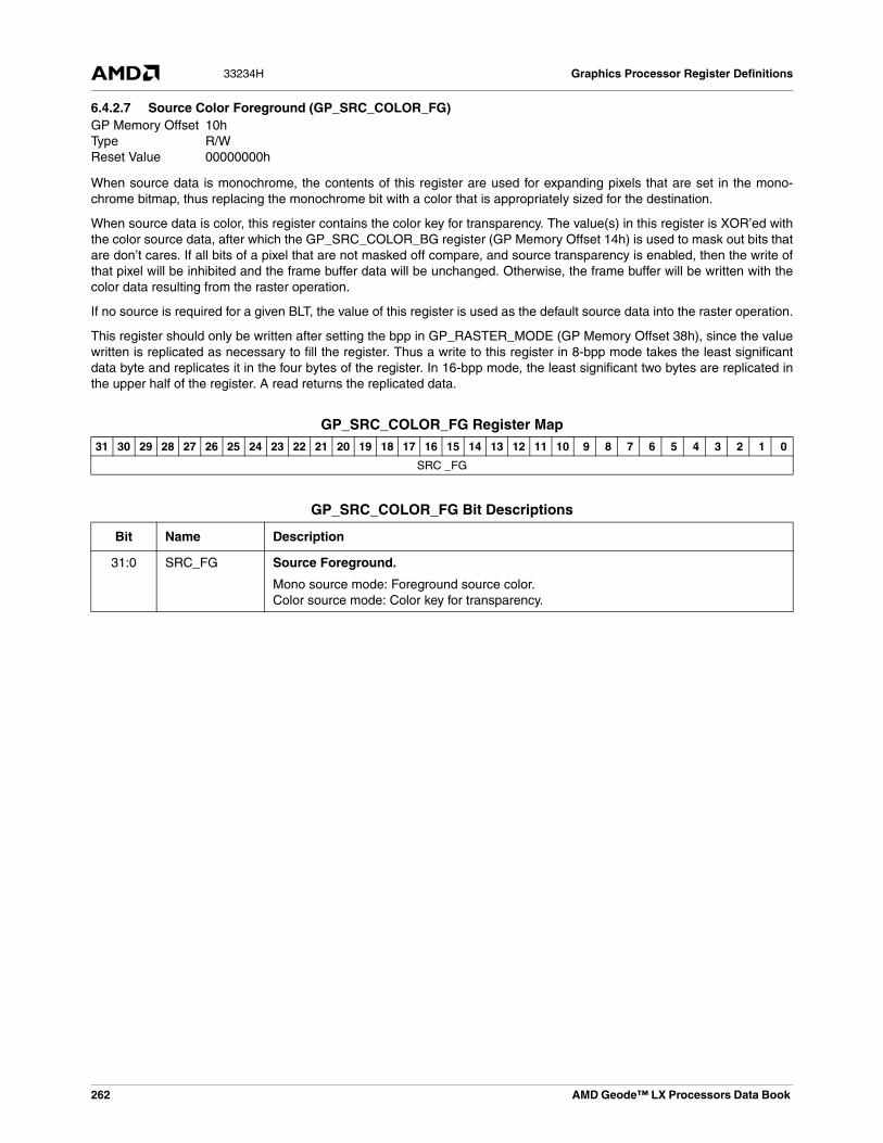
6.4.2.7 Source Color Foreground (GP_SRC_COLOR_FG)
When source data is monochrome, the contents of this register are used for expanding pixels that are set in the mono-chrome bitmap, thus replacing the monochrome bit with a color that is appropriately sized for the destination.
When source data is color, this register contains the color key for transparency. The value(s) in this register is XOR’ed withthe color source data, after which the GP_SRC_COLOR_BG register (GP Memory Offset 14h) is used to mask out bits thatare don’t cares. If all bits of a pixel that are not masked off compare, and source transparency is enabled, then the write ofthat pixel will be inhibited and the frame buffer data will be unchanged. Otherwise, the frame buffer will be written with thecolor data resulting from the raster operation.
If no source is required for a given BLT, the value of this register is used as the default source data into the raster operation.
This register should only be written after setting the bpp in GP_RASTER_MODE (GP Memory Offset 38h), since the valuewritten is replicated as necessary to fill the register. Thus a write to this register in 8-bpp mode takes the least significantdata byte and replicates it in the four bytes of the register. In 16-bpp mode, the least significant two bytes are replicated inthe upper half of the register. A read returns the replicated data.
GP Memory Offset 10hType R/WReset Value 00000000h
GP_SRC_COLOR_FG Register Map31 30 29 28 27 26 25 24 23 22 21 20 19 18 17 16 15 14 13 12 11 10 9 8 7 6 5 4 3 2 1 0
SRC _FG
GP_SRC_COLOR_FG Bit Descriptions
Bit Name Description
31:0 SRC_FG Source Foreground.
Mono source mode: Foreground source color.Color source mode: Color key for transparency.

AMD Geode™ LX Processors Data Book 263
Graphics Processor Register Definitions 33234H
6.4.2.8 Source Color Background (GP_SRC_COLOR_BG)
When source data is monochrome, the contents of this register are used for expanding pixels that are clear in the mono-chrome bitmap, thus replacing the monochrome bit with a color that is appropriately sized for the destination.
When source data is color, this register contains the color key mask for transparency. The value(s) in this register areinverted and OR’ed with the result of the compare of the source data and the GP_SRC_COLOR_FG register. Thus, a bitthat is clear implies that bit position is a don’t care for transparency, and a bit that is set implies that bit position must matchin both the source data and GP_SRC_COLOR_FG register. If the result of the OR produces all ones for an entire pixel andtransparency is enabled, then the write of that pixel is inhibited and the destination data is unchanged.
This register should only be written after setting the BPP/FMT bits in GP_RASTER_MODE (GP Memory Offset38h[31:28]), since the value written is replicated as necessary to fill the register. Thus a write to this register in 8-bpp modetakes the least significant data byte and replicates it in all four bytes of the register. In 16-bpp mode, the least significant twobytes are replicated in the upper half of the register. A read returns the replicated data.
GP Memory Offset 14hType R/WReset Value 00000000h
GP_SRC_COLOR_BG Register Map31 30 29 28 27 26 25 24 23 22 21 20 19 18 17 16 15 14 13 12 11 10 9 8 7 6 5 4 3 2 1 0
SRC _BG
GP_SRC_COLOR_BG Bit Descriptions
Bit Name Description
31:0 SRC_BG Source Background.
Mono source mode: Background source color.Color source mode: Color key mask for transparency.
264 AMD Geode™ LX Processors Data Book
Graphics Processor Register Definitions33234H
6.4.2.9 Pattern Color (GP_PAT_COLOR_x)
In solid pattern mode, the pattern hardware is disabled and GP_PAT_COLOR_0 is selected as the input to the raster oper-ation.
In monochrome pattern mode, GP_PAT_COLOR_0 and GP_PAT_COLOR_1 are used for expanding the monochrome pat-tern into color. A clear bit in the pattern is replaced with the color stored in GP_PAT_COLOR_0 and a set bit in the patternis replaced with the color stored in GP_PAT_COLOR_1.
In color pattern mode, these registers each hold part of the pattern according to Table 6-30.
These registers should only be written after setting the BPP/FMT and PM bits in GP_RASTER_MODE (GP Memory Offset38h[31:28, 9:8]), since the value written may be replicated if necessary to fill the register. If the pattern is color, no replica-tion is performed and the data is written to the registers exactly as it is received. If the pattern is monochrome, the writedata is expanded if the color depth is less than 32-bpp. Thus a write to these registers in 8-bpp monochrome pattern modetakes the least significant data byte and replicates it in the four bytes of the register. In 16-bpp monochrome pattern mode,the least significant two bytes are replicated in the upper half of the register. A read returns the replicated data.
GP Memory Offset 18h GP_PAT_COLOR_01Ch GP_PAT_COLOR_1 20h GP_PAT_COLOR_224h GP_PAT_COLOR_328h GP_PAT_COLOR_42Ch GP_PAT_COLOR_5
Type R/WReset Value 00000000h
Table 6-30. PAT_COLOR Usage for Color Patterns
Register 8-bpp Mode 16-bpp Mode 32-bpp Mode
GP_PAT_COLOR_0 Line 1, pixels 3-0 Line 0, pixels 5-4 Line 0, pixel 2
GP_PAT_COLOR_1 Line 1, pixels 7-4 Line 0, pixels 7-6 Line 0, pixel 3
GP_PAT_COLOR_2 Line 2, pixels 3-0 Line 1, pixels 1-0 Line 0, pixel 4
GP_PAT_COLOR_3 Line 2, pixels 7-4 Line 1, pixels 3-2 Line 0, pixel 5
GP_PAT_COLOR_4 Line 3, pixels 3-0 Line 1, pixels 5-4 Line 0, pixel 6
GP_PAT_COLOR_5 Line 3, pixels 7-4 Line 1, pixels 7-6 Line 0, pixel 7
GP_PAT_COLOR_x Register Map31 30 29 28 27 26 25 24 23 22 21 20 19 18 17 16 15 14 13 12 11 10 9 8 7 6 5 4 3 2 1 0
PAT_COLOR_x
GP_PAT_COLOR_x Bit Descriptions
Bit Name Description
31:0 PAT_COLOR_x Pattern Color x.
Mono pattern mode: Pattern color for expansion.Color pattern mode: Color pattern.

AMD Geode™ LX Processors Data Book 265
Graphics Processor Register Definitions 33234H
6.4.2.10 Pattern Data (GP_PAT_DATA_x)
In solid pattern mode, these registers are not used.
In monochrome pattern mode, GP_PAT_DATA_0 and GP_PAT_DATA_1 combine to hold the entire 8x8 pattern (64 bits).GP_PAT_DATA_0[7:0] is the first line of the pattern, with bit 7 corresponding to the leftmost pixel on the screen.GP_PAT_DATA_1[31:24] is the last line of the pattern.
In color pattern mode, these registers each hold part of the pattern according to Table 6-31.
6.4.2.11 Raster Mode (GP_RASTER_MODE)
This register controls the manipulation of the pixel data through the graphics pipeline. Refer to section Section 6.3.10 "Ras-ter Operations (ROP)" on page 251 for more information on the functionality of the ROP and Section 6.3.11 "Image Com-positing Using Alpha" on page 252 for information on alpha blending and compositing. This register is byte writable to allowmodification of the ROP and other control bits without having to rewrite the BPP and FMT every time.
GP Memory Offset 30h GP_PAT_DATA_034h GP_PAT_DATA_1
Type R/WReset Value 00000000h
Table 6-31. PAT_DATA Usage for Color Patterns
Register 8-bpp Mode 16-bpp Mode 32-bpp Mode
GP_PAT_DATA_0 Line 0, pixels 3-0 Line 0, pixels 1-0 Line 0, pixel 0
GP_PAT_DATA_1 Line 0, pixels 7-4 Line 0, pixels 3-2 Line 0, pixel 1
GP_PAT_DATA_x Register Map31 30 29 28 27 26 25 24 23 22 21 20 19 18 17 16 15 14 13 12 11 10 9 8 7 6 5 4 3 2 1 0
PAT_DATA_x
GP_PAT_DATA_x Bit Descriptions
Bit Name Description
31:0 PAT_DATA_x Pattern Data x.
Mono pattern mode: Pattern data.Color pattern mode: Color pattern.
GP Memory Offset 38hType R/WReset Value 00000000h
GP_RASTER_MODE Register Map31 30 29 28 27 26 25 24 23 22 21 20 19 18 17 16 15 14 13 12 11 10 9 8 7 6 5 4 3 2 1 0
BPP/FMT RSVD EN OS AS CS RSVD SI PI ST PT PM ROP/aR

266 AMD Geode™ LX Processors Data Book
Graphics Processor Register Definitions33234H
GP_RASTER_MODE Bit Descriptions
Bit Name Description
31:28 BPP/FMT Color Depth and Format.
0000: 8-bpp, 3:3:2 format.0100: 16-bpp, 4:4:4:4 format.0101: 16-bpp, 1:5:5:5 format.0110: 16-bpp, 0:5:6:5 format.1000: 32-bpp, 8:8:8:8 format.All Others: Undefined.
27:24 RSVD Reserved. Write as read.
23:22 EN Alpha Enable Bits. Also used to select how to apply the specified operation.
00: Alpha disabled/ROP enabled.
01: Alpha operation applies to only the RGB values of the pixel. Output alpha is from channel B if the OS is 01; otherwise from channel A.
10: Alpha operation applies to only the alpha of the pixel. Output RGB is from channel B if the OS is 01; otherwise from channel A.
11: Alpha operation applies to all channels of the pixel (ARGB).
21:20 OS Alpha Operation Select. Determines the alpha operation to be performed if enabled.
00: a∗A.01: (1-a)*B.10: A + (1-a)*B.11: a∗A + (1-a)*B.
* Channel A is added in this case only if the selected α is also from channel A.
19:17 AS Alpha Select. Chooses which alpha value to use for the multiplication.
000: aA 100: ColorA001: aB 101: ColorB010: aR 110: aR
011: Constant 1 111: Constant 1
16 CS Channel Select. Determines which data stream gets put on which channel.
0: A is source, B is destination.1: A is destination, B is source.
15:14 RSVD Reserved. Write as read.
13 SI Source Invert. Inverts the sense of monochrome source data.
12 PI Pattern Invert. Inverts the sense of monochrome pattern data.
11 ST Source Transparency. Enables transparency for monochrome source data and color keying for color source data.
0: Disable.1: Enable.
10 PT Pattern Transparency. Enables transparency for monochrome pattern data.
0: Disable.1: Enable.
9:8 PM Pattern Mode. Specifies the format of the pattern data.
00: Solid pattern. Pattern data always sourced from GP_PAT_COLOR_0 (GP Memory Offset 18h).
01: Mono pattern.10: Color pattern.11: Undefined.

AMD Geode™ LX Processors Data Book 267
Graphics Processor Register Definitions 33234H
6.4.2.12 Vector Mode (GP_VECTOR_MODE)
Writing to this register configures the vector mode and initiates the rendering of the vector. If a BLT or vector operation isalready in progress when this register is written, the BLT pending bit in GP_BLT_STATUS (GP Memory Offset 44h)is setand the vector is queued to begin when the current operation is complete. Software should not write to any register (otherthan GP_HOST_SRC if required) while the BLT pending bit is set since it will corrupt the pending vector operation. Settingthe TH bit causes the vector operation to wait until the next VBLANK before beginning rendering. Software may still queueanother operation behind a throttled vector as long as the BLT pending bit is clear.
7:0 ROP/aR Raster Operations (ROP). Combination rule for source, pattern and destination when performing raster operations. (See Section 6.3.10 "Raster Operations (ROP)" on page 251.)
Alpha Value (aR). Alpha value that can be used for some of the alpha compositing oper-ations.
GP Memory Offset 3ChType WOReset Value 00000000h
GP_RASTER_MODE Bit Descriptions (Continued)
Bit Name Description
GP_VECTOR_MODE Register Map31 30 29 28 27 26 25 24 23 22 21 20 19 18 17 16 15 14 13 12 11 10 9 8 7 6 5 4 3 2 1 0
RSVD CP TH DR DN DJ YJ
GP_VECTOR_MODE Bit Descriptions
Bit Name Description
31:6 RSVD Reserved. Write to 0.
5 CP Checkpoint. Generates interrupt when this vector is completed if checkpoint interrupt is enabled.
4 TH Throttle.
0: Operation begins immediately.1: Operation waits until next VBLANK before beginning.
3 DR Destination Required.
0: Destination data is not needed for operation.1: Destination data is needed from frame buffer.
2 DN Minor Direction.
0: Negative minor axis step.1: Positive minor axis step.
1 DJ Major Direction.
0: Negative major axis step.1: Positive major axis step
0 YJ Y Major.
0: X major vector.1: Y major vector.

268 AMD Geode™ LX Processors Data Book
Graphics Processor Register Definitions33234H
6.4.2.13 BLT Mode (GP_BLT_MODE)
Writing to this register configures the BLT mode and initiates the rendering of the BLT. If a BLT or vector operation is alreadyin progress when this register is written, the BLT pending bit in GP_BLT_STATUS (GP Memory Offset 44h) is set and theBLT is queued to begin when the current operation is complete. Software should not write to any register (other thanGP_HOST_SRC if required) while the BLT pending bit is set since it will corrupt the pending BLT. Setting the TH bit causesthe BLT operation to wait until the next VBLANK before beginning. Software may still queue another operation behind athrottled BLT as long as the BLT pending bit is clear.
GP Memory Offset 40hType WOReset Value 00000000h
GP_BLT_MODE Register Map31 30 29 28 27 26 25 24 23 22 21 20 19 18 17 16 15 14 13 12 11 10 9 8 7 6 5 4 3 2 1 0
RSVD CP TH X Y SM RSVD DR SR
GP_BLT_MODE Bit Descriptions
Bit Name Description
31:12 RSVD Reserved. Write to 0.
11 CP Checkpoint. Generates interrupt when this BLT is completed if checkpoint interrupt is enabled.
10 TH Throttle. BLT does not begin until next VBLANK.
0: Disable.1: Enable.
9 X X Direction.
0: Indicates a positive increment for the X position.1: Indicates a negative increment for the X position.
8 Y Y Direction.
0: Indicates a positive increment for the Y position.1: Indicates a negative increment for the Y position.
7:6 SM Source Mode. Specifies the format of the source data.
00: Source is color bitmap.01: Source is unpacked monochrome.10: Source is byte-packed monochrome.11: Undefined.
5:3 RSVD Reserved. Write as read.
2 DR Destination Required.
0: No destination data is required.1: Indicates that destination data is needed from frame buffer.
1:0 SR Source Required.
00: No source data.01: Source from frame buffer.10: Source from GP_HST_SRC register (GP Memory Offset 48h).11: Undefined.

AMD Geode™ LX Processors Data Book 269
Graphics Processor Register Definitions 33234H
6.4.2.14 Status and Reset (GP_BLT_STATUS, GP_RESET)
This register is used to provide software with the current status of the GP in regards to operations pending and currentlyexecuting. A write to this register has no effect unless byte 3 is 69h, which causes a reset of the GP, losing all state informa-tion and discarding any active or pending BLT or vector. This is only intended to be used during debug to restore the GP inthe event of a hang. It is not required as part of the initialization or power on sequence for GP.
6.4.2.15 Host Source (GP_HST_SRC)
This register is used by software to load source data that is not originated in the frame buffer memory region. When per-forming a BLT that requires host source data, software should first set up all of the configuration registers that are requiredand initiate the BLT by writing to the GP_BLT_MODE register (GP Memory Offset 40h). This initiates the BLT in hardware,which then waits for writes to the GP_HST_SRC register. Software should then perform enough writes to this register tocomplete the BLT operation. Writes to this register are moved immediately into the source FIFO, allowing the CPU to per-form successive writes. The EH bit in the GP_BLT_STATUS (GP Memory Offset 44h[5]) register indicates that the GP canaccept another cache line (32 bytes) of data.
This register is also aliased to the address range 100h-3FFh to allow the processor to move large blocks of data to the GPthrough the repeat MOVS instruction. The GP throttles the incoming data by holding off register writes on the GLIU whenthe source FIFO is full.
GP Memory Offset 44hType ROReset Value 00000008h
GP_BLT_STATUS Register Map31 30 29 28 27 26 25 24 23 22 21 20 19 18 17 16 15 14 13 12 11 10 9 8 7 6 5 4 3 2 1 0
RSVD UF RP EH CE SHE PP IN PB
GP_BLT_STATUS Bit Descriptions
Bit Name Description
31:8 RSVD Reserved.
7 UF Underflow. If bit is set, Channel 3 had too few pixels to complete the BLT.
6 RP Read Pending. If bit is set, read request is waiting for data from GLIU.
5 EH Expecting Host Source Data. If bit is set, current BLT is expecting to receive host source data on Channel 3.
4 CE Command Buffer Empty. If bit is set, read and write pointers are equal.
3 SHE Source FIFO Half Empty. If bit is set, source FIFO can accept another cache line of host source data.
2 PP Primitive Pending. If bit is set, a second BLT or vector is in the queue behind the currently executing operation.
1 IN Interrupt Pending. If bit is set, the GP interrupt signal is active.
0 PB Primative Busy. If bit is set, an operation is currently executing in the GP.
GP Memory Offset 48hType WOReset Value xxxxxxxxh
GP_HST_SRC Register Map31 30 29 28 27 26 25 24 23 22 21 20 19 18 17 16 15 14 13 12 11 10 9 8 7 6 5 4 3 2 1 0
HST_SRC

270 AMD Geode™ LX Processors Data Book
Graphics Processor Register Definitions33234H
6.4.2.16 Base Offset (GP_BASE_OFFSET)
This register is used to define the physical base addresses of the regions used for all GP read and write operations to mem-ory. Each base defines a 16 MB region that begins on a 4 MB boundary. Thus the top two bits of the offset [23:22] areadded to the base to identify the correct 4 MB region in memory for a given transfer. Because there are different basesdefined for each potential source of data, each can come from a different memory region. If a memory operation goesbeyond the 16 MB region that has been assigned, it wraps back to the beginning of the 16 MB region.
6.4.2.17 Command Top (GP_CMD_TOP)
This register defines the starting address of the command buffer within the command buffer region. Bits [23:0] of this regis-ter are combined with the CBASE in GLD_MSR_CONFIG (MSR A0002001h) to form the 32-bit address. This registershould only be changed when the GP is not actively executing out of the command buffer, which can be checked by readingthe CE bit in the GP_BLT_STATUS register (GP Memory Offset 44h[4]) or by verifying that GP_CMD_READ (GP MemoryOffset 58h) and GP_CMD_WRITE (GP Memory Offset 5Ch) have the same value.
GP_HST_SRC Bit Descriptions
Bit Name Description
31:0 HST_SRC Host Source Data. Used during BLT in host source mode.
GP Memory Offset 4ChType R/WReset Value 01004010h
GP_BASE_OFFSET Register Map31 30 29 28 27 26 25 24 23 22 21 20 19 18 17 16 15 14 13 12 11 10 9 8 7 6 5 4 3 2 1 0
DBASE SBASE CH3BASE RSVD
GP_BASE_OFFSET Bit Descriptions
Bit Name Description
31:22 DBASE Destination Base. Base address of destination data region in physical memory.
21:12 SBASE Source Base. Base address of source data region in physical memory.
11:2 CH3BASE Channel 3 Base. Base address of channel 3 data region in physical memory.
1:0 RSVD Reserved.
GP Memory Offset 50hType R/WReset Value 01000000h
GP_CMD_TOP Register Map31 30 29 28 27 26 25 24 23 22 21 20 19 18 17 16 15 14 13 12 11 10 9 8 7 6 5 4 3 2 1 0
RSVD CMD_TOP RSVD
GP_CMD_TOP Bit Descriptions
Bit Name Description
31:24 RSVD Reserved. Read returns 0.
23:5 CMD_TOP Command Top. Starting address of the command buffer in the command buffer region.
4:0 RSVD Reserved. Read returns 0.

AMD Geode™ LX Processors Data Book 271
Graphics Processor Register Definitions 33234H
6.4.2.18 Command Bottom (GP_CMD_BOT)
This register defines the ending address of the command buffer within the command buffer region. Bits [23:0] of this registerare combined with the CBASE in GLD_MSR_CONFIG (MSR A0002001h) to form the 32 bit address. This register shouldonly be changed when the GP is not actively executing out of the command buffer, which can be checked by reading the CEbit in GP_BLT_STATUS (GP Memory Offset 44h[4]) or by verifying that GP_CMD_READ and GP_CMD_WRITE (GP Mem-ory Offset 58h and 5Ch respectively) have the same value.
6.4.2.19 Command Read (GP_CMD_READ)
This register points to the location from which the GP fetches the next command buffer data. As data is fetched, this registerincrements. When this register equals GP_CMD_BOT (GP Memory Offset 54h) and the data has been fetched, it isreloaded with the value from GP_CMD_TOP (GP Memory Offset 50h). If the current command buffer had the W (wrap) bitset in the command word, then this register is reset to GP_CMD_TOP after the execution of the current command buffer.Typically, this register is read only by the software, and is used in combination with GP_CMD_WRITE (GP Memory Offset5Ch) to determine how much space is available in the command buffer for new commands. However, this register can bewritten. A write to this register also affects the GP_CMD_WRITE register such that when creating and initializing a newcommand buffer in memory, the read and write pointers can be updated simultaneously to point to the beginning of thebuffer without the GP thinking that the buffer was non-empty and beginning to fetch. This register must not be written whilethe GP is actually executing command buffers as this could cause the GP to hang.
GP Memory Offset 54hType R/WReset Value 00FFFFE0h
GP_CMD_BOT Register Map31 30 29 28 27 26 25 24 23 22 21 20 19 18 17 16 15 14 13 12 11 10 9 8 7 6 5 4 3 2 1 0
RSVD CMD_BOT RSVD
GP_CMD_BOT Bit Descriptions
Bit Name Description
31:24 RSVD Reserved. Read returns 0.
23:5 CMD_BOT Command Bottom. Ending address of the command buffer in the command buffer region.
4:0 RSVD Reserved. Read returns 0.
GP Memory Offset 58hType R/WReset Value 00000000h
GP_CMD_READ Register Map31 30 29 28 27 26 25 24 23 22 21 20 19 18 17 16 15 14 13 12 11 10 9 8 7 6 5 4 3 2 1 0
RSVD CMD_READ
GP_CMD_READ Bit Descriptions
Bit Name Description
31:24 RSVD Reserved. Read returns 0.
23:0 CMD_READ Command Read. Pointer to the tail of the command buffer in the command buffer region.

272 AMD Geode™ LX Processors Data Book
Graphics Processor Register Definitions33234H
6.4.2.20 Command Write (GP_CMD_WRITE)
This register points to the next location to be written with command buffer data from the processor. After the processorwrites out a complete command buffer starting at this address, it should write to this register to update the value to point tothe next location to be written. This write is what queues the GP that there is command buffer data that needs to be fetchedand activates the command buffer logic within GP. If the Wrap bit is set in a command buffer control WORD, this registershould be written with the same value as that found in GP_CMD_TOP (GP Memory Offset 50h) after the CPU has com-pleted loading the command buffer in memory.
6.4.2.21 Offset (GP_CH3_OFFSET)
The GP_CH3_OFFSET register is used during a BLT to give a starting location for the BLT data in the channel 3 region ofmemory. The register consists of two fields to compose the address, the OFFSET and Nibble Select. The OFFSET field isa pointer, which when added to the channel 3 base address, gives the memory location of the byte containing the first pixelof the BLT. As in the destination and source offsets, this value must be aligned correctly for BLT direction and pixel depth.When host source data is used, the two LSBs of OFFSET must still be initialized with the byte location of the first sourcepixel in the host source data stream. Nibble Select is used when the source is 4-bpp, to give an offset within the specifiedbyte to the nibble representing the starting pixel. Both the OFFSET LSBs and Nibble Select are used to index into the firstDWORD of every new line of source data.
For a rotation of 90° counterclockwise, the offset should point to the top rightmost byte of the source bitmap. For a rotationof 90° clockwise, the offset should point to the bottom leftmost byte of the source bitmap. For a rotation of 180°, the offsetshould point to the opposite corner from that pointed to by the destination offset (e.g., If GP_BLT_MODE (GP Memory Off-set 40h) indicates a left to right, top to bottom fill, then the destination offset should point to the upper left corner and thechannel 3 offset should point to the bottom right most byte of the source bitmap).
GP Memory Offset 5ChType R/WReset Value 00000000h
GP_CMD_WRITE Register Map31 30 29 28 27 26 25 24 23 22 21 20 19 18 17 16 15 14 13 12 11 10 9 8 7 6 5 4 3 2 1 0
RSVD CMD_WRITE
GP_CMD_WRITE Bit Descriptions
Bit Name Description
31:24 RSVD Reserved. Read returns 0.
23:0 CMD_WRITE Command Write. Pointer to where the next command buffer will be written in the com-mand buffer region.
GP Memory Offset 60hType R/WReset Value 00000000h
GP_CH3_OFFSET Register Map31 30 29 28 27 26 25 24 23 22 21 20 19 18 17 16 15 14 13 12 11 10 9 8 7 6 5 4 3 2 1 0
YLSBS XLSBS N
RS
VD OFFSET

AMD Geode™ LX Processors Data Book 273
Graphics Processor Register Definitions 33234H
6.4.2.22 Stride (GP_CH3_MODE_STR)
The GP_ CH3_MODE_STR register has multiple uses. The STRIDE field is used to indicate the byte width of the channel 3bitmaps. Whenever the Y coordinate is incremented, this value is added (or subtracted if the Y bit is set) to (from) the previ-ous start address to generate the start address for the next line. Stride values up to 64 KB minus one are supported.
The remaining fields of this register describe the type, size and source of the channel 3 data. The output of channel 3 canbe used to replace either source or pattern data into the ROP unit. The PS bit is used to select which pipeline the data willbe placed on. If the FMT indicates that the incoming data is alpha, then the incoming data can be used as alpha data in thealpha blend unit if the AS bits in the GP_RASTER_MODE (GP Memory Offset 38h[19:17]) register are set to 110. If theBPP/FMT bits in the GP_RASTER_MODE register (bits [31:28]) indicate the output pixel is 32-bpp, then the incoming alphadata is converted to 8 bits and is consumed at the rate of one pixel per clock. If the BPP/FMT bits are set for 16-bpp, thenthe incoming alpha data is converted to 4 bits and is consumed at the rate of two pixels per clock. Alpha blending is not sup-ported in 8-bpp mode.
Some operating systems store color data in reverse color order (Blue/Green/Red). This data can be converted into the cor-rect display order by setting the BGR bit. This works for all input formats except for alpha, so if the incoming data is alpha,do not set this bit.
Rotation is controlled by the RO bit. If this bit is set, the direction of rotation is determined by the X and Y bits. When this bitis set, the GP_DST_OFFSET (GP Memory Offset 00h) should point to the upper left corner of the destination and the Xand Y bits in the GP_BLT_MODE (GP Memory Offset 40h[9,8]) should not be set. The output must be left to right, top tobottom. The output is actually written in horizontal strips, 8, 16 or 32 pixels high and as wide as the output. For 8-bpp rota-tion, 1K of buffer space is the minimum required to perform the operation. Having 2K available allows data to be prefetchedwhile the previous tile is being written out. Setting the PL bit limits the buffer size to 1K as it preserves the LUT data in theother 1K of the buffer. This bit should be set when performing any indexed color BLT or if it is likely that the LUT data thathas been loaded will be needed again for a future BLT. The performance is higher when this bit is not set.
GP_CH3_OFFSET Bit Descriptions
Bit Name Description
31:29 YLSBS YLSBS. Y coordinate of starting pixel within color pattern memory.
28:26 XLSBS XLSBS. X coordinate of starting pixel within color pattern memory.
25 N Nibble Select. Nibble address for 4-bpp pixels/alpha. 0 starts at the leftmost nibble, 1 starts at the rightmost.
24 RSVD Reserved. Write as read.
23:0 OFFSET Offset. Offset from the channel 3 base address to the first source pixel.
GP Memory Offset 64hType R/WReset Value 00000000h
GP_CH3_MODE_STR Register Map31 30 29 28 27 26 25 24 23 22 21 20 19 18 17 16 15 14 13 12 11 10 9 8 7 6 5 4 3 2 1 0
EN PS X Y BPP/FMT RO BGR PM PL PE HS RSVD STRIDE
GP_CH3_MODE_STR Bit Descriptions
Bit Name Description
31 EN Enable.
0: Channel 3 is off. Old pipelines behave exactly as they used to.1: Channel 3 is on. Data is forced into either source or pattern pipeline from channel 3.
30 PS Pipeline Select.
0: Channel 3 data directed to/replaces old pattern pipeline.1: Channel 3 data directed to/replaces old source pipeline

274 AMD Geode™ LX Processors Data Book
Graphics Processor Register Definitions33234H
29 X X Direction for Fetch. Data is reversed if fetch direction does not match destination direction.
0: Left to right direction.1: Right to left direction.
28 Y Y Direction for Fetch. Data is reversed if fetch direction does not match destination direction.
0: Top to bottom direction.1: Bottom to top direction.
27:24 BPP/FMT Color Depth and Format of Input.
0000: 8-bpp 3:3:2.0001: 8-bpp indexed.0010: 8-bpp alpha.0100: 16-bpp 4:4:4:4.0110: 16-bpp 0:5:6:5.0111: 4:2:2 YUV.1000: 32-bpp.1011: 24-bpp packed.1101: 4-bpp indexed.1110: 4-bpp alpha.All others: Undefined.
23 RO Rotate Bitmap.
0: Disable rotation.1: Enable rotation direction determined by X and Y. See Section 6.3.2.1 "Rotating BLTs"
on page 242.
22 BGR BGR Mode (applies only when 16-bpp or 32-bpp).
0: Pass through (or YUY2 for 4:2:2 mode).1: Swap red and blue channels on output (or UYVY for 4:2:2 mode).
21 PM Pattern Mode.
0: Bitmap mode, data from memory or host source.1: Pattern mode.
20 PL Preserve LUT Data.
0: Entire 2K buffer available for fetch data.1: 1K reserved for LUT.
19 PE Prefetch Enable. When this bit is set, data may be fetched while the BLT is still pending.
18 HS Host Source.
0: Data fetched from memory.1: Data written through host source writes.
17:16 RSVD Reserved.
15:0 STRIDE Stride. Increment between lines of bitmap in bytes.
GP_CH3_MODE_STR Bit Descriptions (Continued)
Bit Name Description

AMD Geode™ LX Processors Data Book 275
Graphics Processor Register Definitions 33234H
6.4.2.23 Width/Height (GP_CH3_WIDHI)
This register is used to specify the width and the height of the bitmap to be fetched on channel 3 in pixels. This need notmatch the destination width and height, as in the case of a rotation BLT where the width and height are swapped, but thetotal number of pixels should be equal to the number of pixels in the destination.
6.4.2.24 Host Source (GP_CH3_HSRC)
This register is used by software to load channel 3 data when the channel 3 pattern mode bit is not set, the channel 3enable bit is set, and the channel 3 host source bit is set.This register is also aliased to the address range 400h-FFFhallowing the processor to load large blocks of data to the GP using the repeat MOVS instruction.
GP Memory Offset 68hType R/WReset Value 00000000h
GP_CH3_WIDHI Register Map31 30 29 28 27 26 25 24 23 22 21 20 19 18 17 16 15 14 13 12 11 10 9 8 7 6 5 4 3 2 1 0
RSVD WID RSVD HI
GP_CH3_WIDHI Bit Descriptions
Bit Name Description
31:28 RSVD Reserved. Write as read.
27:16 WID Width. Width in pixels of the BLT operation.
15:12 RSVD Reserved. Write as read.
11:0 HI Height. Height in pixels of the BLT operation.
GP Memory Offset 6ChType WOReset Value xxxxxxxxh
GP_CH3_HSRC Register Map31 30 29 28 27 26 25 24 23 22 21 20 19 18 17 16 15 14 13 12 11 10 9 8 7 6 5 4 3 2 1 0
HST_SRC
GP_CH3_HSRC Bit Descriptions
Bit Name Description
31:0 HST_SRC Host Source Data. Used during BLT in host source mode
276 AMD Geode™ LX Processors Data Book
Graphics Processor Register Definitions33234H
6.4.2.25 LUT Index (GP_LUT_INDEX)
This register is used to initialize the LUT_INDEX pointer that is used for subsequent LUT operations. All LUT accesses areDWORD accesses so only the 9 LSBs of the pointer are used to index into the 2 KB LUT. Addresses 000h-0FFh are usedfor 8-bit indexed LUT data. Addresses 000h-00Fh are used for 4-bit indexed LUT data. Addresses 100h-13Fh are used forstoring color patterns. All addresses are used for storing incoming data (unless the PL bit is set in theGP_CH3_MODE_STR register, GP Memory Offset 64h[20]), but none of the remaining addresses have any significance tosoftware.
6.4.2.26 LUT Data (GP_LUT_DATA)
This register is used to store data into the LUT for indexed color translations and color patterns. The 32 bits written to thisregister are stored in the LUT at the location specified in the GP_LUT_INDEX register (GP Memory Offset 70h). A read ofthis register returns the contents of the LUT at the location specified by the GP_LUT_INDEX register. Either a read or writeof this register will cause the GP_LUT_INDEX register to increment, so the LUT can be loaded through successive writes tothe GP_LUT_DATA register.
GP Memory Offset 70hType R/WReset Value 00000000h
GP_CH3_HSRC Register Map31 30 29 28 27 26 25 24 23 22 21 20 19 18 17 16 15 14 13 12 11 10 9 8 7 6 5 4 3 2 1 0
RSVD LUT_INDEX
GP_CH3_HSRC Bit Descriptions
Bit Name Description
31:9 RSVD Reserved.
8:0 LUT_INDEX LUT Index. Used to initialize the LUT_INDEX pointer that is used for subsequent LUT operations. The LUT_INDEX automatically increments on a write to the GP_LUT_DATA register (GP Memory Offset 74h). When performing a read, bit 31 must be set to cause the hardware to perform the read and update the GP_LUT_DATA register. If this bit is not set, then a write is assumed and the read will not be performed.
GP Memory Offset 74hType R/WReset Value xxxxxxxxh
GP_CH3_HSRC Register Map31 30 29 28 27 26 25 24 23 22 21 20 19 18 17 16 15 14 13 12 11 10 9 8 7 6 5 4 3 2 1 0
LUT_DATA
GP_CH3_HSRC Bit Descriptions
Bit Name Description
31:0 LUT_DATA LUT_DATA. Used to store data into the LUT for indexed color translations and color pat-terns.
AMD Geode™ LX Processors Data Book 277
Graphics Processor Register Definitions 33234H
6.4.2.27 Interrupt Control (GP_INT_CNTRL)
This register is used to control the interrupt signal from the GP. It contains a 16-bit mask and a 16-bit interrupt detect. Themask portion is read/write. A bit set in the mask register disables the corresponding interrupt bit. At reset, all interrupts aredisabled. The interrupt detect bits are automatically set by the hardware to indicate that the corresponding condition hasoccurred and that the mask bit for that condition is not set. The interrupt detect bits remain set until they are cleared by awrite to the GP_INT_CNTRL register. Writing a 1 to an interrupt detect bit clears the bit. Writing a 0 to an interrupt detect bithas no effect. Therefore, all of the interrupts in the GP may be cleared by reading the GP_INT_CNTRL register and writingback the value that was read. Whenever any of the interrupt detect bits are set in this register, the IN bit will be set in theGP_BLT_STATUS register (GP Memory Offset 44h[1]).
GP Memory Offset 78hType R/WReset Value 0000FFFFh
GP_INT_CNTRL Register Map31 30 29 28 27 26 25 24 23 22 21 20 19 18 17 16 15 14 13 12 11 10 9 8 7 6 5 4 3 2 1 0
RSVD I1 I0 RSVD M1 M0
GP_INT_CNTRL Bit Descriptions
Bit Name Description
31:18 RSVD Reserved. Read returns 0.
17 I1 GP Idle Detect Interrupt.
16 I0 Command Buffer Empty Detect Interrupt.
15:2 RSVD Reserved. Read returns 1.
1 M1 GP Idle Mask Bit.
0 M0 Command Buffer Empty Mask Bit.

278 AMD Geode™ LX Processors Data Book
Display Controller33234H
6.5 Display ControllerThe Display Controller (DC) module retrieves graphics,video, and overlay streams from the frame buffer, serial-izes the streams, performs any necessary color lookupsand output formatting, and interfaces to the VP for drivingthe display device.
Features
• 512x64-bit display FIFO
• 64x64x2-bit hardware cursor
• 64x vertical resolution x2-bit hardware icon overlay
• 3x261x8-bit palette/gamma RAM (including five exten-sion colors)
• Display refresh compression
• 64x64-bit compressed line buffer
• Flexible timing generator
• Support for Video Blanking Interval (VBI) data
• Support for interlaced modes up to 1920x1080
• 3-tap flicker filter for support of interlaced NTSC and PAL display modes
• Flexible memory addressing
• Video overlay support
• Independent VGA block for complete hardware VGA implementation
• Dirty/Valid RAM and controller to monitor memory traffic in support of display refresh compression
• Six 512x64-bit line buffers to support downscaling and flicker filtering
• 3x5-tap graphics filter for scaling and filtering
The DC module consists of a GUI (Graphical User Inter-face) block, a VGA block, and back-end scaling/filter. TheGUI is compatible with the Display Controller found in theGX processor. The VGA block provides hardware compati-bility with the VGA graphics standard. The GUI and VGAblocks share a single display FIFO and display refreshmemory interface to the memory controller. The VGA blockpasses 8-bpp and syncs to the GUI, which expands thepixels to 24-bpp via the CLUT (color lookup table). TheVGA block also passes the information to the graphics filterfor scaling and interlaced display support. This stream isthen passed to the Video Processor (VP), which is used forvideo overlay. The VP forwards this information to the DAC(Digital-to-Analog Converter), which generates the analogred, green, and blue signals and buffers the sync signals,that are then sent to the display. The VP output can also berendered as YUV data that can be output on the Video Out-put Port. The DC block diagram is shown in Figure 6-12.
Figure 6-12. Display Controller High-Level Block Diagram
VGA Block
Graphical User Interface Block
FIFO
Host I/F
FIFO
Pixel, Syncs, DISPEN
Display Memory I/F
Display RefreshMemory Control
8-Bit Pixel,Syncs, Display enable
CTL
Dirty/Valid Flags
Video Data Output to VP
Dirty/Valid RAMand Control
GLIU0 Port
GLIU0 Memory Port
GeodeLink™Interface
Unit 0(GLIU0)
CLUTGraphicsScaler/Filter
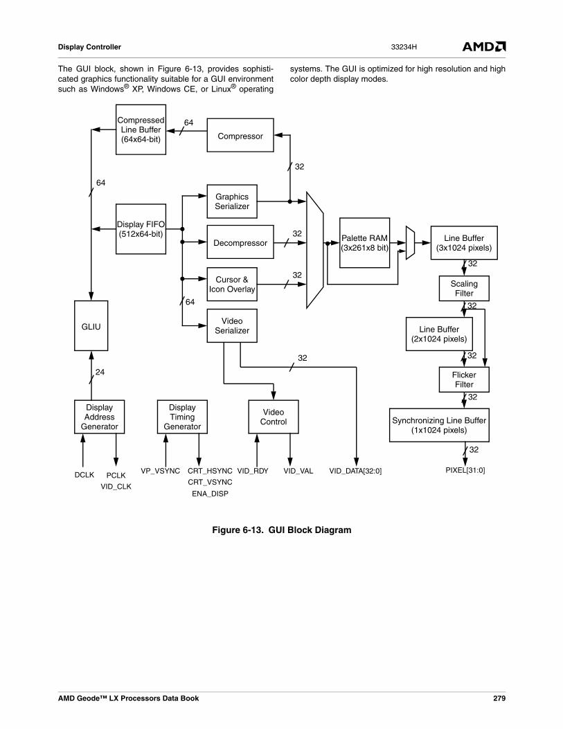
AMD Geode™ LX Processors Data Book 279
Display Controller 33234H
The GUI block, shown in Figure 6-13, provides sophisti-cated graphics functionality suitable for a GUI environmentsuch as Windows® XP, Windows CE, or Linux® operating
systems. The GUI is optimized for high resolution and highcolor depth display modes.
Figure 6-13. GUI Block Diagram
Compressed
Graphics
Decompressor
Cursor &
Display FIFO
Compressor
Video
32
32
64
64
64
Display
24
Display
CRT_HSYNC
CRT_VSYNC
ENA_DISP
DCLK PCLK
VID_CLK
VID_DATA[32:0] PIXEL[31:0]
32
Video
VID_RDY VID_VALVP_VSYNC
TimingGenerator
Control
Serializer
AddressGenerator
Icon Overlay
(512x64-bit)
Serializer
Line Buffer(64x64-bit)
GLIU
32
Palette RAM(3x261x8 bit)
Line Buffer(3x1024 pixels)
ScalingFilter
Line Buffer(2x1024 pixels)
FlickerFilter
Synchronizing Line Buffer(1x1024 pixels)
32
32
32
32
32

280 AMD Geode™ LX Processors Data Book
Display Controller33234H
The VGA block, shown in Figure 6-14, provides hardwaresupport for a compatible VGA solution. It consists of anindependent CRT controller and pixel formatting units. Italso provides the standard VGA host memory data manip-
ulation functions such as color compare, set, reset, etc.This block provides complete support for all VGA text andgraphics modes.
Figure 6-14. VGA Block Diagram
CRTC Pixel Formatter
Shared FIFO
FIFO Control
Syncs
DISPEN
Syncs
DISPEN
8-bit PixelClock Control
Display Memory I/F Control
Display Memory I/F Data
FIFO R/W Data
FIFO Control
FIFO Read Data
VGA DAC I/O Unit
Host Memory I/F Unit
Host CPU I/F GUI CLUT I/O Control
Host Memory I/F
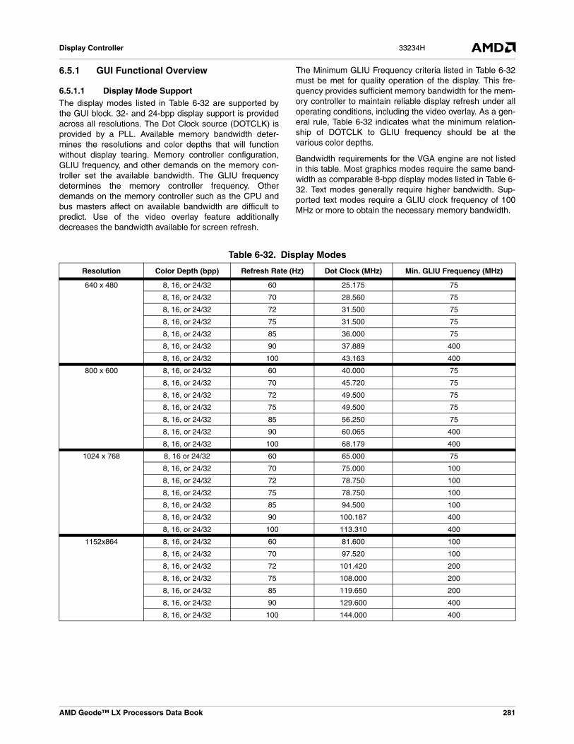
AMD Geode™ LX Processors Data Book 281
Display Controller 33234H
6.5.1 GUI Functional Overview
6.5.1.1 Display Mode SupportThe display modes listed in Table 6-32 are supported bythe GUI block. 32- and 24-bpp display support is providedacross all resolutions. The Dot Clock source (DOTCLK) isprovided by a PLL. Available memory bandwidth deter-mines the resolutions and color depths that will functionwithout display tearing. Memory controller configuration,GLIU frequency, and other demands on the memory con-troller set the available bandwidth. The GLIU frequencydetermines the memory controller frequency. Otherdemands on the memory controller such as the CPU andbus masters affect on available bandwidth are difficult topredict. Use of the video overlay feature additionallydecreases the bandwidth available for screen refresh.
The Minimum GLIU Frequency criteria listed in Table 6-32must be met for quality operation of the display. This fre-quency provides sufficient memory bandwidth for the mem-ory controller to maintain reliable display refresh under alloperating conditions, including the video overlay. As a gen-eral rule, Table 6-32 indicates what the minimum relation-ship of DOTCLK to GLIU frequency should be at thevarious color depths.
Bandwidth requirements for the VGA engine are not listedin this table. Most graphics modes require the same band-width as comparable 8-bpp display modes listed in Table 6-32. Text modes generally require higher bandwidth. Sup-ported text modes require a GLIU clock frequency of 100MHz or more to obtain the necessary memory bandwidth.
Table 6-32. Display Modes
Resolution Color Depth (bpp) Refresh Rate (Hz) Dot Clock (MHz) Min. GLIU Frequency (MHz)
640 x 480 8, 16, or 24/32 60 25.175 75
8, 16, or 24/32 70 28.560 75
8, 16, or 24/32 72 31.500 75
8, 16, or 24/32 75 31.500 75
8, 16, or 24/32 85 36.000 75
8, 16, or 24/32 90 37.889 400
8, 16, or 24/32 100 43.163 400
800 x 600 8, 16, or 24/32 60 40.000 75
8, 16, or 24/32 70 45.720 75
8, 16, or 24/32 72 49.500 75
8, 16, or 24/32 75 49.500 75
8, 16, or 24/32 85 56.250 75
8, 16, or 24/32 90 60.065 400
8, 16, or 24/32 100 68.179 400
1024 x 768 8, 16 or 24/32 60 65.000 75
8, 16, or 24/32 70 75.000 100
8, 16, or 24/32 72 78.750 100
8, 16, or 24/32 75 78.750 100
8, 16, or 24/32 85 94.500 100
8, 16, or 24/32 90 100.187 400
8, 16, or 24/32 100 113.310 400
1152x864 8, 16, or 24/32 60 81.600 100
8, 16, or 24/32 70 97.520 100
8, 16, or 24/32 72 101.420 200
8, 16, or 24/32 75 108.000 200
8, 16, or 24/32 85 119.650 200
8, 16, or 24/32 90 129.600 400
8, 16, or 24/32 100 144.000 400

282 AMD Geode™ LX Processors Data Book
Display Controller33234H
1280 x 1024 8, 16, or 24/32 60 108.000 200
8, 16, or 24/32 70 129.600 200
8, 16, or 24/32 72 133.500 200
8, 16, or 24/32 75 135.000 200
8, 16, or 24/32 85 157.500 200
8, 16, or 24/32 90 172.800 400
8, 16, or 24/32 100 192.000 400
1600 x 1200 8, 16, or 24/32 60 162.000 200
8, 16, or 24/32 70 189.000 200
8, 16, or 24/32 72 198.000 233
8, 16, or 24/32 75 202.500 233
8, 16, or 24/32 85 229.500 266
8, 16, or 24/32 90 251.182 400
8, 16, or 24/32 100 280.640 400
1920x1440 8, 16, or 24/32 60 234.000 266
8, 16, or 24/32 70 278.400 400
8, 16, or 24/32 72 288.000 400
8, 16, or 24/32 75 297.000 400
8, 16, or 24/32 85 341.349 400
Television Modes
720x483 SD NTSC up to 32 59.94i 27.000 200
640x480 SD NTSC up to 32 up to 60.00i 27.000 200
768x576 SD PAL up to 32 50.00i 27.000 200
720x576 SD PAL up to 32 50.00i 27.000 200
1280x720 HD up to 32 up to 60.00i up to 74.750 200
1280x768 HD up to 32 50.00i 74.750 200
1440x720 HD up to 32 60.00i 74.750 400
1440x768 HD up to 32 50.00i 74.750 400
1920x1080 HD up to 32 up to 60.00i up to 148.500 400
Table 6-32. Display Modes (Continued)
Resolution Color Depth (bpp) Refresh Rate (Hz) Dot Clock (MHz) Min. GLIU Frequency (MHz)
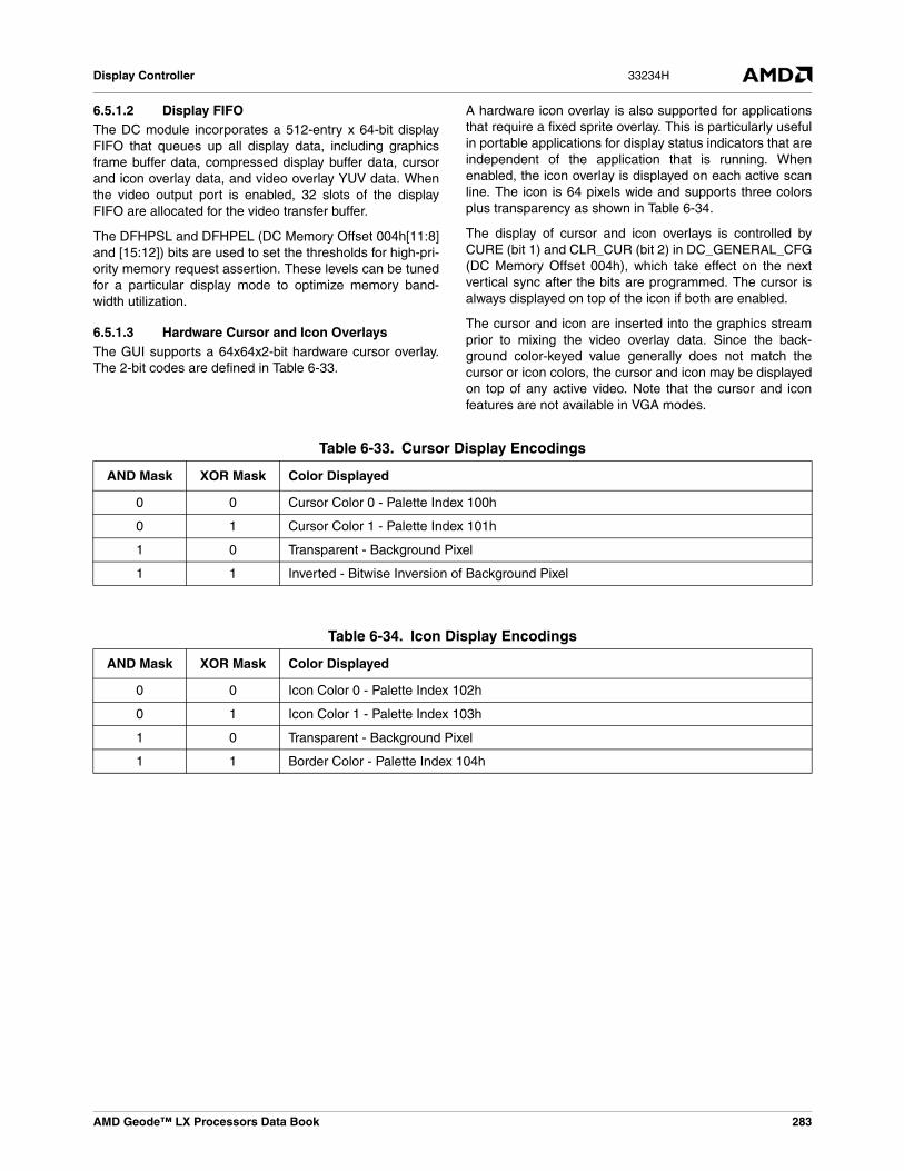
AMD Geode™ LX Processors Data Book 283
Display Controller 33234H
6.5.1.2 Display FIFOThe DC module incorporates a 512-entry x 64-bit displayFIFO that queues up all display data, including graphicsframe buffer data, compressed display buffer data, cursorand icon overlay data, and video overlay YUV data. Whenthe video output port is enabled, 32 slots of the displayFIFO are allocated for the video transfer buffer.
The DFHPSL and DFHPEL (DC Memory Offset 004h[11:8]and [15:12]) bits are used to set the thresholds for high-pri-ority memory request assertion. These levels can be tunedfor a particular display mode to optimize memory band-width utilization.
6.5.1.3 Hardware Cursor and Icon OverlaysThe GUI supports a 64x64x2-bit hardware cursor overlay.The 2-bit codes are defined in Table 6-33.
A hardware icon overlay is also supported for applicationsthat require a fixed sprite overlay. This is particularly usefulin portable applications for display status indicators that areindependent of the application that is running. Whenenabled, the icon overlay is displayed on each active scanline. The icon is 64 pixels wide and supports three colorsplus transparency as shown in Table 6-34.
The display of cursor and icon overlays is controlled byCURE (bit 1) and CLR_CUR (bit 2) in DC_GENERAL_CFG(DC Memory Offset 004h), which take effect on the nextvertical sync after the bits are programmed. The cursor isalways displayed on top of the icon if both are enabled.
The cursor and icon are inserted into the graphics streamprior to mixing the video overlay data. Since the back-ground color-keyed value generally does not match thecursor or icon colors, the cursor and icon may be displayedon top of any active video. Note that the cursor and iconfeatures are not available in VGA modes.
Table 6-33. Cursor Display Encodings
AND Mask XOR Mask Color Displayed
0 0 Cursor Color 0 - Palette Index 100h
0 1 Cursor Color 1 - Palette Index 101h
1 0 Transparent - Background Pixel
1 1 Inverted - Bitwise Inversion of Background Pixel
Table 6-34. Icon Display Encodings
AND Mask XOR Mask Color Displayed
0 0 Icon Color 0 - Palette Index 102h
0 1 Icon Color 1 - Palette Index 103h
1 0 Transparent - Background Pixel
1 1 Border Color - Palette Index 104h

284 AMD Geode™ LX Processors Data Book
Display Controller33234H
Cursor/Icon Buffer FormatsIn 2-bpp mode, the cursor buffer is stored as a linear dis-play buffer containing interlaced AND and XOR QWORDs(8-byte segments). Each QWORD contains the appropriatemask for 64 pixels. Even QWORDs contain the ANDmasks and odd QWORDs contain the XOR masks. Themasks are stored “in display order” with the leftmost pixelbeing most significant and the rightmost pixel being leastsignificant.
For 32-bpp cursors, the cursor pixels include an alphavalue, and are alpha blended with the underlying graphicspixels. For the purposes of cursor overlay, the cursor alphavalue is used. If the graphics stream includes an alphavalue, that value is not used for the purposes of cursoroverlay. However, the graphics alpha value is retained inthe resulting pixel stream.
The cursor buffer stores 192 bytes of data per scan line (for48 horizontal pixels) in 32-bpp mode. In this mode, the cur-sor size is 48 pixels wide and 64 pixels high, and so thebuffer is 12 KB in size.
In 2-bpp mode, cursor buffer includes 16 bytes of data perscan line (for 64 horizontal pixels). The cursor is 64x64,therefore the cursor buffer is 1 KB in size.
The DC contains logic to address the overlay of the cursoron top of a color key region. Table 6-35 indicates what pixelvalue is output from the DC’s rendering engine when thecursor is overlayed on the color key region.
Note that this behavior varies slightly when the graphicsare represented in 32-bpp mode, which includes a per-pixel alpha value.
Table 6-35. Cursor/Color Key/Alpha Interaction
Cursor Per-Pixel AlphaColor Key Match, Per-Pixel Alpha No Per-Pixel Alpha
Color Key Match, No Per-Pixel Alpha
No Cursor COLOR = graphics color
ALPHA = graphics alpha
COLOR = graphics color
ALPHA = 00
COLOR = graphics color
ALPHA = FF
COLOR = graphics color
ALPHA = 00
2-bpp Cursor(cursor color)
COLOR = cursor color
ALPHA = graphics alpha or FF (config-urable)
COLOR = cursor color
ALPHA = FF
COLOR = cursor color
ALPHA = FF
COLOR = cursor color
ALPHA = FF
2-bpp Cursor(invert color)
COLOR = invert graph-ics color
ALPHA = graphics alpha or FF (config-urable)
COLOR = invert graphics color
ALPHA = FF
COLOR = invert graphics color
ALPHA = FF
COLOR = invert graphics color
ALPHA = FF
2-bpp Cursor(transparent)
COLOR = graphics color
ALPHA = graphics alpha
COLOR = graphics color
ALPHA = 00
COLOR = graphics color
ALPHA = FF
COLOR = graphics color
ALPHA = 00
Color Cursor(with alpha)
COLOR = blend cur-sor/graphics
ALPHA = pp alpha or FF (configurable)
COLOR = cursor color
ALPHA = cursor alpha
COLOR = blend cursor/graphics
ALPHA = FF
COLOR = cursor color
ALPHA = cursor alpha

AMD Geode™ LX Processors Data Book 285
Display Controller 33234H
6.5.1.4 Display Refresh CompressionTo reduce the system memory contention caused by thedisplay refresh, the GUI block contains compression anddecompression logic for compressing the frame bufferimage in real time as it is sent to the display. The DC doesnot modify the standard frame buffer, but rather, it utilizes aseparate compressed display buffer for updating the dis-play under certain conditions. This compressed displaybuffer can be allocated within the extra off-screen memorywithin the graphics memory region.
Coherency of the compressed display buffer is maintainedby use of dirty and valid bits for each line. Whenever a linehas been successfully compressed, it is retrieved from thecompressed display buffer for all future accesses until theline becomes dirty again. Dirty lines are retrieved from thenormal uncompressed frame buffer.
The compression logic has the ability to insert a “static”frame every other display frame, during which time dirtybits are ignored and the valid bits are read to determinewhether a line should be retrieved from the frame buffer orcompressed display buffer. This allows a latency of oneframe between pixels actually being rendered and showingup on the display. This effect typically goes unnoticed fortraditional 2D applications but may result in increased tear-ing in single-buffered animation sequences. This featuremay be used to tune for maximum performance or optimaldisplay quality.
The compression algorithm used commonly achieves com-pression ratios between 10:1 and 50:1, depending on thenature of the display data. The compression algorithmemployed is lossless and therefore results in no loss ofvisual quality. This high level of compression provideshigher system performance by reducing typical latency fornormal system memory access, higher graphics perfor-mance by increasing available drawing bandwidth to thememory subsystem, and lower power consumption by sig-nificantly reducing the number of off-chip memoryaccesses required for refreshing the display. These advan-tages become more pronounced as display resolution,color depth, and refresh rate are increased, and as the sizeof the installed DRAM increases.
As uncompressed lines are fed to the display, they arecompressed and stored in an on-chip compressed linebuffer (64x64 bits). Lines will not be written back to thecompressed display buffer in the DRAM unless a success-ful compression has resulted, so there is no penalty forpathological frame buffer images where the compressionalgorithm is sub-optimal.
6.5.1.5 Dirty/Valid RAMThe DC module incorporates the Dirty/Valid RAM(DVRAM) in the Display Controller module. The Dirty/ValidRAM controller directly snoops GLIU0 request packets onthe memory data port.
The Dirty/Valid RAM may be used to monitor locations inmemory other than the frame buffer. (Compression anddecompression must be disabled in order for the DisplayController to continue to function properly.) This may beused for scenarios where software (or the Graphics Pro-cessor) must modify or re-render a frame whenever corre-sponding modifications occur in an offscreen graphicsbuffer. The “palletized” bit is set upon writes to the corre-sponding region of memory. However, it is up to softwareto clear the dirty bit by writing to the Dirty/Valid RAMAccess register (DC Memory Offset 08Ch).
6.5.1.6 Palette/Gamma RAMThe GUI block contains a 261x24 color lookup table RAMused for palletized display modes (Indexes 0-255), cursorcolors (Indexes 256-257), and the GUI mode border color(Index 260). This color lookup table is also used by theVGA block to map the 8-bit VGA pixels to a 24-bit RGBcolor value. In true color display modes (16, 24, or 32-bpp),the color lookup table can be used as a gamma correctionRAM.
6.5.1.7 Display Address GeneratorThe GUI block supports flexible address generation for theframe buffer, compressed display buffer, cursor and iconbuffers, and video buffers (YUV 4:2:2 or 4:2:0 format). Aseparate start offset register is provided for each displaybuffer. The start offset may be programmed to be relativeto frame buffer space (up to 256 MB).
6.5.1.8 Display Timing GeneratorThe GUI block includes a flexible timing generator capableof handling up to a 1920x1440 resolution display. Horizon-tal timings are programmable with 1-pixel granularity. Verti-cal timings are programmable with scan line granularity.The timing registers are master-slaved such that a new tim-ing set may be programmed while the working set is stillactive. The TRUP configuration bit (DC_DISPLAY_CFG,DC Memory Offset 008h[6]) is used to allow the new set oftimings to take effect at the start of vertical sync. As long asthe horizontal and vertical total counts do not change whena new timing set is loaded, the sync pulses should remainstable and the display should not glitch.
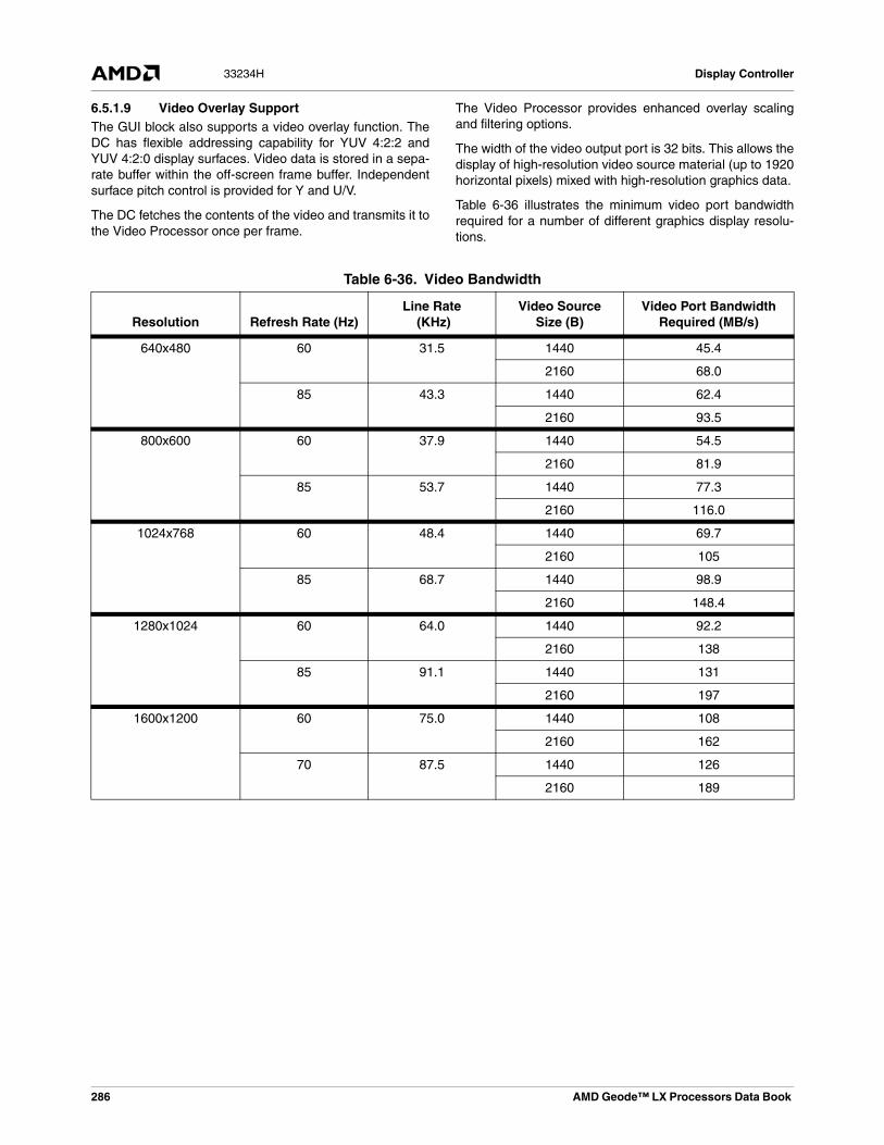
286 AMD Geode™ LX Processors Data Book
Display Controller33234H
6.5.1.9 Video Overlay SupportThe GUI block also supports a video overlay function. TheDC has flexible addressing capability for YUV 4:2:2 andYUV 4:2:0 display surfaces. Video data is stored in a sepa-rate buffer within the off-screen frame buffer. Independentsurface pitch control is provided for Y and U/V.
The DC fetches the contents of the video and transmits it tothe Video Processor once per frame.
The Video Processor provides enhanced overlay scalingand filtering options.
The width of the video output port is 32 bits. This allows thedisplay of high-resolution video source material (up to 1920horizontal pixels) mixed with high-resolution graphics data.
Table 6-36 illustrates the minimum video port bandwidthrequired for a number of different graphics display resolu-tions.
Table 6-36. Video Bandwidth
Resolution Refresh Rate (Hz)Line Rate
(KHz)Video Source
Size (B)Video Port Bandwidth
Required (MB/s)
640x480 60 31.5 1440 45.4
2160 68.0
85 43.3 1440 62.4
2160 93.5
800x600 60 37.9 1440 54.5
2160 81.9
85 53.7 1440 77.3
2160 116.0
1024x768 60 48.4 1440 69.7
2160 105
85 68.7 1440 98.9
2160 148.4
1280x1024 60 64.0 1440 92.2
2160 138
85 91.1 1440 131
2160 197
1600x1200 60 75.0 1440 108
2160 162
70 87.5 1440 126
2160 189

AMD Geode™ LX Processors Data Book 287
Display Controller 33234H
6.5.1.10 Output Formats
Video Output Data SequencingThe order that video data is transmitted from the DC to theVP depends on the format of the video data. For YUV 4:2:0mode, the entire stream of Y data is transmitted for asource line, followed by the entire stream of U data for theline, and finally, the entire stream of V data for the line. Thesize of the U and V streams are always one-half the size ofthe Y stream. The data is not interlaced as in the YUV 4:2:2mode. The data ordering is shown in Table 6-37.
For YUV 4:2:2 mode, YUV data is interlaced in a singlestream, with a maximum size of 1440 bytes.
In YUV 4:2:2 mode, four orders of YUV data are supported.The data format is selectable via the Video Configurationregister (VP Memory Offset 000h) in the Video Processormodule. The data ordering is shown in Table 6-38.
6.5.2 VBI DataVBI (Video Blanking Interval) data is fetched by the DC atthe start of each frame. The data is fetched from a buffer inmemory, separately from video or graphics data. It is pre-sented to the VP on the graphics port. VBI data is providedvia a path that circumvents the gamma correction paletteand the graphics filter. The data presented to the VP/VOPis only the data in memory. There are no additional head-ers attached by the DC. Configuration registers in the DCdetermine how many lines of VBI data are sent during eachfield; the lines can be enabled/disabled independently ofone another. If a line is disabled, no data is fetched (frommemory) for that line, and the memory line pointer is NOTincremented. Thus, non-contiguous lines of screen VBImust be stored contiguously in memory if there are noactive VBI lines between them. The DC can be pro-grammed to fetch multiple fields worth of VBI data from lin-ear frame buffer space without resetting to the start of thebuffer on each field. This minimizes the interrupt overheadrequired to manage VBI data. VBI data streams of up to 4KB per scan line are supported.
The VBI horizontal timings are controlled in a manner simi-lar to the horizontal active timings. The reference point forthe horizontal (pixel) counter is the start of active video.This means that if the VBI data is to be active before thispoint on the line (i.e., to the left of, and above active video),it may be necessary to set the VBI horizontal start point toa large number (less than the horizontal total, but largerthan the VBI horizontal end point). The line counter used tocalculate VBI offsets is incremented at the start of eachHSYNC, and NOT at the start of active video. This meansthat even if the VBI horizontal timings are such that it startsduring the horizontal “back porch” region, the line countsand enables are the same as if the VBI horizontal timingwas the same as the graphics timing.
6.5.3 GenLockThe DC has the ability to use an external source to deter-mine the timing and frequency of VSYNC. This is primarilyused in systems in which the VIP is providing video data tobe displayed in a native screen resolution and frame rate.The DC can also be configured to detect the loss ofVSYNC in this case, and temporarily generate its ownVSYNC pulse until the external source resumes generationof video data and synchronization. This is accomplishedthrough the use of a VSYNC timeout counter. The DC canalso generate an interrupt when a loss of synchronizationis detected.
Table 6-37. YUV 4:2:0 Video Data Ordering
Sequence Data Type Max Size (Bytes)
1 Y stream 1920
2 U stream 960
3 V stream 960
Table 6-38. YUV 4:2:2 Video Data Ordering
Mode YUV Ordering (Note 1)
Note 1. U = Cb, V = Cr.
0 U Y0 V Y1
1 Y1 V Y0 U
2 Y0 U Y1 V
3 Y0 V Y1 U

288 AMD Geode™ LX Processors Data Book
Display Controller33234H
6.5.4 VGA Block Functional OverviewThe VGA block provides full hardware support for a VGAgraphics subsystem. It is compatible with the IBM VGA asdefined in the IBM Video Subsystem Technical Referencemanual. This section provides an overview of VGA featuresand functions.
6.5.4.1 VGA ModesA VGA “mode” is a programmed VGA configuration definedby the VGA BIOS that produces a graphics frame bufferformat and a screen image with specific characteristics.The base VGA function provides coded text modes for text-based applications, and graphics modes for graphics-based applications. Many of these modes are compatiblewith older graphics adapter standards, such as mono-chrome display adapter, color graphics adapter, andenhanced graphics adapter.
Text ModesThere are five text modes defined by VGA BIOS as shownTable 6-39.
Each of the text modes provides a coded frame buffer con-sisting of a 16-bit value for each character. The low byte isthe ASCII character code for the character to display, andthe high byte is an attribute byte that determines how thecharacter is displayed (foreground, background colors,blink, underline, etc.). There are two formats defined byBIOS for the attribute byte: color and monochrome asshown in Table 6-40.
Graphics ModesThe graphics modes defined by VGA BIOS are shown inTable 6-41.
Figure 6-15. VGA Frame Buffer Organization
Table 6-39. VGA Text Modes
BIOS Mode
#
Screen Size in
CharactersAttribute
TypeBuffer
Address Compatibility
0, 1 40 x 25 Color B8000h-BFFFFh
CGA
2, 3 80 x 25 Color B8000h-BFFFFh
EGA, VGA
7 80 x 25 Mono-chrome
B0000h-B7FFFh
MDA
Table 6-40. Text Mode Attribute Byte Format
Bit Color Definition Monochrome Definition
7 Blink Blink
6 Background Color (R) Background
5 Background Color (G) Background
4 Background Color (B) Background
3 Foreground Intensity/Font Select
Foreground Intensity/Font Select
2 Foreground Color (R) Foreground
1 Foreground Color (G) Foreground
Table 6-41. VGA Graphics Modes
BIOS Mode #Screen Size in
Pixels # of ColorsFrame Buffer
Format Buffer Address
4, 5 320 x 200 4 Packed Pixel B8000h-BFFFFh
6 640 x 200 2 Packed Pixel B8000h-BFFFFh
0xD 320 x 200 16 Planar A0000h-AFFFFh
0xE 640 x 200 16 Planar A0000h-AFFFFh
0xF 640 x 400 4 Planar A0000h-AFFFFh
0x10 640 x 350 16 Planar A0000h-AFFFFh
0x11 640 x 480 2 Planar A0000h-AFFFFh
0x12 640 x 480 16 Planar A0000h-AFFFFh
0x13 320 x 200 256 Packed Pixel A0000h-AFFFFh
3 2 1 0
Byte Byte Byte Byte64 KB
DWORDs

AMD Geode™ LX Processors Data Book 289
Display Controller 33234H
6.5.5.2 Graphics ControllerThe graphics controller manages the CPU interaction withvideo memory, and contains the video serializers that feedthe front end of the attribute controller. Several memory
read and write modes are supported that provide variousforms of acceleration for VGA graphics operations. A high-level diagram of the graphics controller is shown in Figure6-16.
Figure 6-16. Graphics Controller High-level Diagram
Memory Map 3 Data
Memory Map 2 Data
Memory Map 1 Data
Memory Map 0 Data
Write
Read MSerializers
CPU Data
PIX Out
Character Gen Data
Attribute Byte
Each bus is 8 bits except for PIX Out,
Video
Mode
Mode Latch UX
which is 4 bits.Note:

290 AMD Geode™ LX Processors Data Book
Display Controller33234H
6.5.5.3 Write ModesThere are four write modes supported by the graphics con-troller (mode 0, 1, 2, and 3). These write modes provide
assistance to the CPU when the frame buffer is in a planargraphics format. Figure 6-17 shows the data flow logic thatsupports these modes.
Figure 6-17. Write Mode Data Flow
CPU Data [7:0]
RotatorData Rotate [2:0]
Set/Reset [3:0]3 2 1 0
3 2 1 0
BWriteMode2
BBBB
Enable Set/Reset [3:0]
3 2 1 0
Bit Mask [7:0]
-A/+A*BWrite Mode 3
A
Read Data Latch [31:0]
ALUFunction [1:0]
31:24 23:16 15:8 7:0
Map 3Write Data
Map 2Write Data
Map 1Write Data
Map 0Write Data
F
A B A B A B A B
A B A B A B A B
A B
D M S D M S D M S D M S
ND
Memory Maps
88 88
8888
8
8 8 8 8
8

AMD Geode™ LX Processors Data Book 291
Display Controller 33234H
6.5.5.4 Read ModesThere are two read modes provided to assist the CPU withgraphics operations in planar modes. Read mode 0 simplyreturns the frame buffer data. Read mode 1 allows the CPU
to do a single color compare across eight pixels. Figure 6-18 shows the data flow for read modes. Figure 6-19 onpage 292 shows how the color compare logic in Figure 6-18 works.
Figure 6-18. Read Mode Data Flow
Memory Read Data [31:0]
Read Map Select [1:0]
Chain2
Chain4
CPU A[1:0]
Select ReadMap Logic
ReadMode1 B
CPU Read Data [7:0]
In [31:0]
Out [7:0]
Color Compare
In [31:0]
Out [7:0]
Color Compare [3:0]
Color Don’t Care [3:0]
A B
Logic

292 AMD Geode™ LX Processors Data Book
Display Controller33234H
Figure 6-19. Color Compare Operation
8x4 Input AND
Compare Result [7:0]
CC3 CC2 CC1 CC0
Memory Data [31:0]31:24 23:16 15:8 7:0
Color Compare [3:0]3 2 1 0
Color Don’t Care [3:0]3 2 1 0
D[7:0]
CXOR
ORCCx[7:0]
E
Color Compare Block Detail
E C D E C D E C D E C D
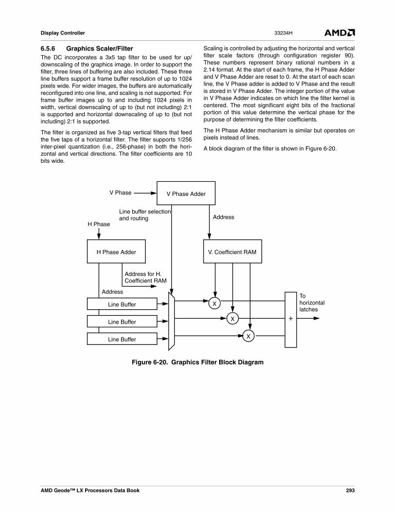
AMD Geode™ LX Processors Data Book 293
Display Controller 33234H
6.5.6 Graphics Scaler/FilterThe DC incorporates a 3x5 tap filter to be used for up/downscaling of the graphics image. In order to support thefilter, three lines of buffering are also included. These threeline buffers support a frame buffer resolution of up to 1024pixels wide. For wider images, the buffers are automaticallyreconfigured into one line, and scaling is not supported. Forframe buffer images up to and including 1024 pixels inwidth, vertical downscaling of up to (but not including) 2:1is supported and horizontal downscaling of up to (but notincluding) 2:1 is supported.
The filter is organized as five 3-tap vertical filters that feedthe five taps of a horizontal filter. The filter supports 1/256inter-pixel quantization (i.e., 256-phase) in both the hori-zontal and vertical directions. The filter coefficients are 10bits wide.
Scaling is controlled by adjusting the horizontal and verticalfilter scale factors (through configuration register 90).These numbers represent binary rational numbers in a2.14 format. At the start of each frame, the H Phase Adderand V Phase Adder are reset to 0. At the start of each scanline, the V Phase adder is added to V Phase and the resultis stored in V Phase Adder. The integer portion of the valuein V Phase Adder indicates on which line the filter kernel iscentered. The most significant eight bits of the fractionalportion of this value determine the vertical phase for thepurpose of determining the filter coefficients.
The H Phase Adder mechanism is similar but operates onpixels instead of lines.
A block diagram of the filter is shown in Figure 6-20.
Figure 6-20. Graphics Filter Block Diagram
V Phase Adder
H Phase Adder V. Coefficient RAM
X
X
X
+
Address
H Phase
V Phase
Line buffer selectionand routing Address
Address for H.Coefficient RAM
Line Buffer
Line Buffer
Line Buffer
Tohorizontallatches
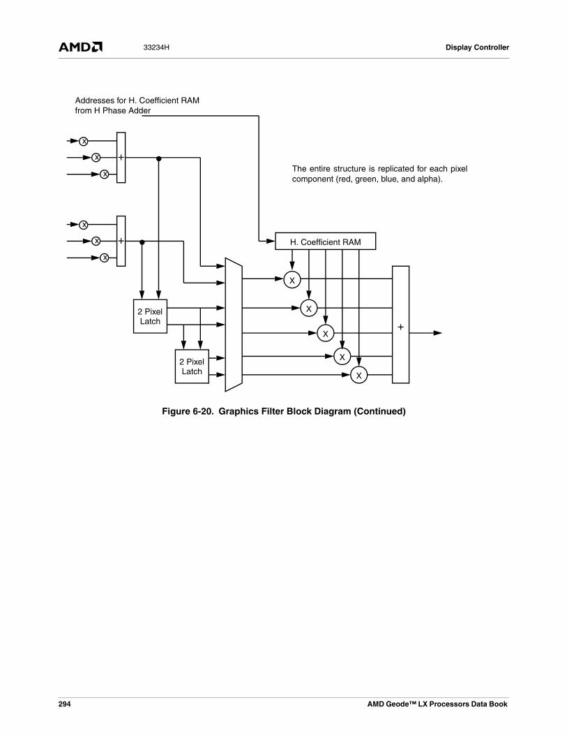
294 AMD Geode™ LX Processors Data Book
Display Controller33234H
Figure 6-20. Graphics Filter Block Diagram (Continued)
2 PixelLatch
x
x
x
+
x
x
x
+
2 PixelLatch
H. Coefficient RAM
X
X
X
X
X
+
Addresses for H. Coefficient RAMfrom H Phase Adder
The entire structure is replicated for each pixelcomponent (red, green, blue, and alpha).
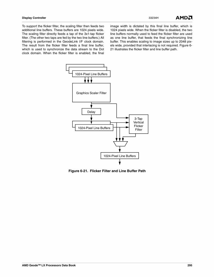
AMD Geode™ LX Processors Data Book 295
Display Controller 33234H
To support the flicker filter, the scaling filter then feeds twoadditional line buffers. These buffers are 1024 pixels wide.The scaling filter directly feeds a tap of the 3x1-tap flickerfilter. (The other two taps are fed by the two line buffers.) Allfiltering is performed in the GeodeLink I/F clock domain.The result from the flicker filter feeds a final line buffer,which is used to synchronize the data stream to the Dotclock domain. When the flicker filter is enabled, the final
image width is dictated by this final line buffer, which is1024 pixels wide. When the flicker filter is disabled, the twoline buffers normally used to feed the flicker filter are usedas one line buffer, that feeds the final synchronizing linebuffer. This enables scaling to image sizes up to 2048 pix-els wide, provided that interlacing is not required. Figure 6-21 illustrates the flicker filter and line buffer path.
Figure 6-21. Flicker Filter and Line Buffer Path
1024-Pixel Line Buffers
Graphics Scaler Filter
Delay
1024-Pixel Line Buffers
3-TapVerticalFlickerFilter
1024-Pixel Line Buffers

296 AMD Geode™ LX Processors Data Book
Display Controller33234H
6.5.7 Color Key EliminationAdditional logic, not shown in the diagrams, is used to pre-serve the color key color. This logic, when enabled, adjuststhe alpha value for each filter input pixel in which a colorkey match is detected. The filter then uses the alpha valueto determine if a pixel matches the color key. For informa-tion on the interaction of cursor and color key, Table 6-35on page 284.
The filter contains specialized logic to remove color key pix-els from the blended output and replace them with nearbypixels. This prevents halo effects if the color key contrastssharply with the surrounding graphics image.
For each of the 3-tap vertical filters, except the center one,the replacement algorithm is as follows:
• If the top pixel is the only color key pixel, the center pixel is used in its place.
• If the bottom pixel is the only color key pixel, the center pixel is used in its place.
• If the center pixel is the only color key pixel, the top pixel is used in its place.
• If any two pixels are color key pixels, the remaining pixel is output to the horizontal filter.
• If all pixels are color key pixels, the bottom pixel is output to the horizontal filter. (The vertical output is a color key pixel and the alpha value is set accordingly.)
For the center 3-tap vertical filter, the algorithm is as fol-lows:
• If the top pixel is a color key pixel, the center pixel is used in its place.
• If the bottom pixel is a color key pixel, the center pixel is used in its place.
• If the center pixel is a color key pixel, the center pixel is output to the horizontal filter regardless of the values of the other two pixels. (The vertical output is a color key pixel, and the alpha value is set accordingly.)
The horizontal filter algorithm follows. Assume that thepixel inputs are numbered 1-5, left to right.
• If pixel 1 is a color key pixel and pixel 2 is not, pixel 2 is used in place of pixel 1.
• If pixel 1 and pixel 2 are both color key pixels, pixel 3 is used in place of pixel 1.
• If pixel 2 is a color key pixel, pixel 3 is used in place of pixel 2.
• If pixel 5 is a color key pixel and pixel 4 is not, pixel 4 is used in place of pixel 5.
• If pixel 4 and pixel 5 are both color key pixels, pixel 3 is used in place of pixel 5.
• If pixel 4 is a color key pixel, pixel 3 is used in place of pixel 4.
• If pixel 3 is a color key pixel, pixel 3 is output from the filter regardless of the values of pixels 1, 2, 4, and 5. (The result is a color key pixel; the alpha value is set accordingly.)
If the center pixel matches the color key, it is passedthrough directly. If the center pixel does not match the colorkey, then any other filter input pixel that matches the colorkey is discarded and replaced by a nearby non-color-key-matching neighbor.
6.5.8 Using the Graphics FilterFrom a software perspective, the AMD Geode LX proces-sor DC appears much like its predecessor in theAMD Geode GX processor design. The graphics filter isdisabled by default, and the timing and addressing regis-ters operate as before. One significant change is the addi-tion of color key detection logic to the DC block. This logicwas previously only in the VP.
When enabling the VP for the purpose of scaling the outputimage, some additional parameters must be programmed(These parameters need not be programmed if the graph-ics filter/scaler is to remain disabled.):
• The horizontal and vertical size of the source image
• The horizontal and vertical scaling factors to be used to scale the source image
• The filter coefficients
The timing registers (DC Memory Offsets 040h-058h)should be programmed based on the parameters for theresulting output image. Note that this image may differ insize from the frame buffer image. The frame buffer imagesize is used to determine the value to be written to theFrame Buffer Active Region Register (DC Memory Offset05Ch).
The scaling factors are programmed into the Graphics Fil-ter Scale Register (DC Memory Offset 090h). These fieldsare 16 bits each (horizontal and vertical). The 16 bits repre-sent the ratio of the destination image size to the sourceimage size. They are right-shifted 14 bits to represent frac-tional values between 0 and 3.99993896484375. However,due to hardware limitations, the downscale factors cannotexceed 2.0. Thus the image can be downscaled by nearly2X in the horizontal and vertical directions. The image canbe upscaled by up to 16384X, although the CRTC does notsupport images beyond 1920x1440 pixels, so it is unlikelythat scale factors beyond about 4X would ever be used.
VBI data is not filtered. The scaling factors in the GraphicsFilter Scale register have no effect on VBI data.
The filter supports 256 sub-pixel phases in both the hori-zontal and vertical directions. Each coefficient is 10 bits,and is represented as a 2’s compliment number, right-shifted 9 bits to represent values between -1 and0.998046875. The coefficients must be loaded into theRAMs by software, using the IRQ/Filter Control register, Fil-ter Coefficient Data register 1, and Filter Coefficient DataRegister 2 (DC Memory Offsets 094h-09Ch).

AMD Geode™ LX Processors Data Book 297
Display Controller 33234H
6.5.9 Interlaced Modes
For interlaced modes, the V_ACTIVE and V_TOTAL fieldsare configured for the odd field. The Even Field VerticalTiming registers (DC Memory Offsets 0E4h-0ECh) areconfigured for the corresponding even field. Figure 6-22 onpage 298 shows a representative timing diagram for theodd and even timing register settings in interlaced modes,and Table 6-43 on page 298 presents the (decimal) timingvalues for some common interlaced modes.
The DC is capable of producing an interlaced output usingany of three separate mechanisms. It can fetch the graph-ics data in an interlaced manner, flicker filter the graphicsdata, or use the same graphics data for both odd and even
fields, (which would effectively line-double the resultingimage). When the VGA is being used, interlaced address-ing is not supported, and scaling must be used. When theframe buffer source image or the output image is widerthan 1024 active pixels, the flicker filter is not supported.
When scaling and/or interleaving is enabled, the size of theframe buffer image (in pixels) will vary from the size of theoutput image. Table 6-42 and Table 6-44 on page 299 indi-cates how the DC’s timing register fields should be pro-grammed for supported scaling and interlacing modes.(Note that for VGA modes, there are several VGA registersthat can affect the size of the frame buffer image. Theseregisters are not enumerated in the table.)
Table 6-42. Programming Image Sizes
Mode
Pre-scale Horizontal Width
Pre-scale Height
Post-scaler Width
Post-scaler Height
Final (Output) Width
Final (Output) Height
Default (no VGA, scal-ing, interlacing, or flicker filter)
H_ACTIVE V_ACTIVE H_ACTIVE V_ACTIVE H_ACTIVE V_ACTIVE
Scaling only FB_H_ACTIVE FB_V_ACTIVE H_ACTIVE V_ACTIVE H_ACTIVE V_ACTIVE
Interlacing only (no flicker filter)
H_ACTIVE V_ACTIVE or V_ACTIVE_EVEN (alternating)
H_ACTIVE V_ACTIVE or V_ACTIVE_EVEN (alternating)
H_ACTIVE V_ACTIVE or V_ACTIVE_EVEN (alternating)
Interlacing with flicker fil-ter
H_ACTIVE V_ACTIVE + V_ACTIVE_EVEN + 1 (Note 1)
H_ACTIVE V_ACTIVE + V_ACTIVE_EVEN + 11
H_ACTIVE V_ACTIVE or V_ACTIVE_EVEN (alternating)
Interlacing with inter-laced addressing (no flicker filter)
H_ACTIVE V_ACTIVE or V_ACTIVE_EVEN (alternating)
H_ACTIVE V_ACTIVE or V_ACTIVE_EVEN (alternating)
H_ACTIVE V_ACTIVE or V_ACTIVE_EVEN (alternating)
Interlacing with scaler (no flicker filter, no interlaced addressing)
FB_H_ACTIVE FB_V_ACTIVE H_ACTIVE V_ACTIVE or V_ACTIVE_EVEN (alternating)
H_ACTIVE V_ACTIVE or V_ACTIVE_EVEN (alternating)
Interlacing with scaler and flicker filter
FB_H_ACTIVE FB_V_ACTIVE H_ACTIVE V_ACTIVE + V_ACTIVE_EVEN + 11
H_ACTIVE V_ACTIVE or V_ACTIVE_EVEN (alternating)
VGA (no scaling, interlac-ing, or flicker filter)
VGA CRTC VGA CRTC VGA CRTC VGA CRTC VGA CRTC VGA CRTC
VGA with scaling (no interlacing or flicker filter
VGA CRTC VGA CRTC H_ACTIVE V_ACTIVE H_ACTIVE V_ACTIVE
VGA with scaling and interlacing (no flicker fil-ter)
VGA CRTC VGA CRTC H_ACTIVE V_ACTIVE or V_ACTIVE_EVEN (alternating)
H_ACTIVE V_ACTIVE or V_ACTIVE_EVEN (alternating)
VGA with scaling, inter-lacing, and flicker filter
VGA CRTC VGA CRTC H_ACTIVE V_ACTIVE + V_ACTIVE_EVEN + 11
H_ACTIVE V_ACTIVE or V_ACTIVE_EVEN (alternating)
Note 1. Because the register value represents the image size minus 1, an additional 1 is added when these two register values are added together to retain the convention.

298 AMD Geode™ LX Processors Data Book
Display Controller33234H
6.5.10 Interlaced Timing ExamplesFigure 6-22 shows how the DC's timing registers are usedto control timings for interlaced display modes. The SMTPEstandards define the even and odd fields as starting atVSYNC, while the register settings define the timingsbased on the start of the active display region, as is com-mon in (non-interlaced) VESA timing standards. As aresult, the V_Sync_End and V_Total register settings eachdefine a region that begins in the odd field and ends in thenext even field. Similarly, the V_Sync_Even_End and
V_Total_Even register settings each define a region thatbegins in the even field and ends in the next odd field.
All register values are in hex; assuming VSYNC pulsewidth of one line.
Table 6-43 lists timings for various interlaced modes for ref-erence. The user should verify these timings against cur-rent specifications for their application.) Table 6-44 on page299 provides the corresponding register settings (hexadec-imal values) for these modes. The VSYNC pulse isassumed to be one line wide. Further information on theseregisters can be found in Section 6.6.5 on page 327.
Figure 6-22. Interlaced Timing Settings
.
VSYNC
Vertical Display Active
Odd Field Even Field
BackPorch
FrontPorch
BackPorch
FrontPorch
Active Region Active Region
V_Active_End
V_Total
V_Sync_Start
V_Sync_End
V_Active_Even_End
V_Total_Even
V_Sync_Even_Start
V_Sync_Even_End
BackPorch
Table 6-43. Vertical Timing in Number of Lines
Timing Set
Odd Field Even Field
Back Porch Active Front Porch Back Porch Active Front Porch
525 16 242 2 17 241 3
625 22 288 2 23 288 2
720i 12 360 3 13 360 2
1080i 20 540 3 20 540 2
1080i 50 Hz 80 540 5 80 540 5

AMD Geode™ LX Processors Data Book 299
Display Controller 33234H
Table 6-44. Timing Register Settings for Interlaced Modes
Timing Set Parameter Odd Register Even Register
Formula V_Active_End (odd_active-1) (even_active-1)
V_Total (odd_active + odd_fp + even_bp - 1) (even_active + even_fp + odd_bp - 1)
V_Sync_Start (odd_active + odd_fp - 1) (even_active + even_fp - 1)
V_Sync_End (odd_active + odd_fp + odd_vsync - 1) (even_active +even_fp + even_vsync - 1)
525 V_Active_End F1 F0
V_Total 106 105
V_Sync_Start F5 F5
V_Sync_End F6 F6
625 V_Active_End 11F 11F
V_Total 138 137
V_Sync_Start 121 121
V_Sync_End 122 122
720i V_Active_End 167 167
V_Total 177 177
V_Sync_Start 16A 169
V_Sync_End 16B 16A
1080i V_Active_End 21B 21B
V_Total 232 231
V_Sync_Start 21E 21D
V_Sync_End 21F 21E
1080i 50 Hz V_Active_End 21B 21B
V_Total 270 270
V_Sync_Start 220 220
V_Sync_End 221 221

300 AMD Geode™ LX Processors Data Book
Display Controller Register Descriptions33234H
6.6 Display Controller Register DescriptionsThis section provides information on the registers associ-ated with the Display Controller (DC) (i.e., GUI and VGAblocks), including the Standard GeodeLink™ Device (GLD)MSRs and the Display Controller Specific MSRs (accessedvia the RDMSR and WRMSR instructions). Table 6-45through Table 6-50 are register summary tables that
include reset values and page references where the bitdescriptions are provided.
Note: The MSR address is derived from the perspectiveof the CPU Core. See Section 4.1 "MSR Set" onpage 45 for more details on MSR addressing.
Table 6-45. Standard GeodeLink™ Device MSRs Summary
MSR Address Type Register Name Reset Value Reference
80002000h RO GLD Capabilities MSR (GLD_MSR_CAP) 00000000_0003E4xxh Page 305
80002001h R/W GLD Master Configuration MSR (GLD_MSR_CONFIG)
00000000_00000000h Page 305
80002002h R/W GLIU0 Device SMI MSR (GLD_MSR_SMI) 00000000_00000000h Page 306
80002003h R/W GLD Error MSR (GLD_MSR_ERROR) 00000000_00000000h Page 308
80002004h R/W GLD Power Management MSR (GLD_MSR_PM)
00000000_00000015h Page 310
80002005h R/W GLIU0 Device Diagnostic MSR (GLD_MSR_DIAG)
00000000_00000000h Page 310
Table 6-46. DC Specific MSRs Summary
MSR Address Type Register Name Reset Value Reference
80000012h R/W DC RAM Control MSR (DC_RAM_CTL_MSR)
00000000_02020202h Page 311
Table 6-47. DC Configuration Control Register Summary
DC Memory Offset Type Register Name Reset Value Reference
Configuration and Status Registers
000h R/W DC Unlock (DC_UNLOCK) 00000000h Page 312
004h R/W DC General Configuration (DC_GENERAL_CFG) 00000000h Page 314
008h R/W DC Display Configuration (DC_DISPLAY_CFG) 00000000h Page 317
00Ch R/W DC Arbitration Configuration (DC_ARB_CFG) 00000000h Page 319
Memory Organization Registers
010h R/W DC Frame Buffer Start Address (DC_FB_ST_OFFSET)
xxxxxxxxh Page 321
014h R/W DC Compression Buffer Start Address (DC_CB_ST_OFFSET)
xxxxxxxxh Page 322
018h R/W DC Cursor Buffer Start Address (DC_CURS_ST_OFFSET)
xxxxxxxxh Page 322

AMD Geode™ LX Processors Data Book 301
Display Controller Register Descriptions 33234H
020h R/W DC Video Y Buffer Start Address Offset (DC_VID_Y_ST_OFFSET)
xxxxxxxxh Page 323
024h R/W DC Video U Buffer Start Address Offset (DC_VID_U_ST_OFFSET)
xxxxxxxxh Page 323
028h R/W DC Video V Buffer Start Address Offset (DC_VID_V_ST_OFFSET)
xxxxxxxxh Page 324
02Ch R/W DC Dirty/Valid Region Top (DC_DV_TOP) 00000000h Page 324
030h R/W DC Line Size (DC_LINE_SIZE) xxxxxxxxh Page 325
034h R/W DC Graphics Pitch (DC_GFX_PITCH) xxxxxxxxh Page 326
038h R/W DC Video YUV Pitch (DC_VID_YUV_PITCH) xxxxxxxxh Page 326
Timing Registers
040h R/W DC Horizontal and Total Timing (DC_H_ACTIVE_TIMING)
xxxxxxxxh Page 328
044h R/W DC CRT Horizontal Blanking Timing (DC_H_BLANK_TIMING)
xxxxxxxxh Page 329
048h R/W DC CRT Horizontal Sync Timing (DC_H_SYNC_TIMING)
xxxxxxxxh Page 329
050h R/W DC Vertical and Total Timing (DC_V_ACTIVE_TIMING)
xxxxxxxxh Page 330
054h R/W DC CRT Vertical Blank Timing (DC_V_BLANK_TIMING)
xxxxxxxxh Page 331
058h R/W DC CRT Vertical Sync Timing (DC_V_SYNC_TIMING)
xxxxxxxxh Page 331
05Ch R/W DC Frame Buffer Active Region Register (DC_FB_ACTIVE)
xxxxxxxxh Page 332
Cursor Position and Count Status Registers
060h R/W DC Cursor X Position (DC_CURSOR_X) xxxxxxxxh Page 332
064h R/W DC Cursor Y Position (DC_CURSOR_Y) xxxxxxxxh Page 333
06Ch RO DC Line Count/Status (DC_LINE_CNT/STATUS) xxxxxxxxh Page 333
Palette Access and FIFO Diagnostic Registers
070h R/W DC Palette Address (DC_PAL_ADDRESS) xxxxxxxxh Page 335
074h R/W DC Palette Data (DC_PAL_DATA) xxxxxxxxh Page 336
078h R/W DC Display FIFO Diagnostic (DC_DFIFO_DIAG) xxxxxxxxh Page 336
07Ch R/W DC Compression FIFO Diagnostic (DC_CFIFO_DIAG)
xxxxxxxxh Page 337
Video Downscaling Registers
080h R/W DC Video Downscaling Delta (DC_VID_DS_DELTA) 00000000h Page 338
GLIU0 Control Registers
084h R/W DC GLIU0 Memory Offset (DC_GLIU0_MEM_OFFSET)
00000000h Page 339
088h R/W DC Dirty/Valid RAM Control (DC_DV_CTL) 00000000h Page 339
Table 6-47. DC Configuration Control Register Summary (Continued)
DC Memory Offset Type Register Name Reset Value Reference
302 AMD Geode™ LX Processors Data Book
Display Controller Register Descriptions33234H
08Ch R/W DC Dirty/Valid RAM Access (DC_DV_ACCESS) 0000000xh Page 340
Graphics Scaling Control Registers
090h R/W DC Graphics Filter Scale (DC_GFX_SCALE) 40004000h Page 341
094h R/W DC IRQ/Filter Control (DC_IRQ_FILT_CTL) 00000000h Page 342
098h R/W DC Filter Coefficient Data Register 1 (DC_FILT_COEFF1)
xxxxxxxxh Page 343
09Ch R/W DC Filter Coefficient Data Register 2 (DC_FILT_COEFF2)
xxxxxxxxh Page 344
VBI Control Registers
0A0h R/W DC VBI Even Control (DC_VBI_EVEN_CTL) xxxxxxxxh Page 344
0A4h R/W DC VBI Odd Control (DC_VBI_ODD_CTL) xxxxxxxxh Page 345
0A8h R/W DC VBI Horizontal Control (DC_VBI_HOR) xxxxxxxxh Page 345
0ACh R/W DC VBI Odd Line Enable (DC_VBI_LN_ODD) xxxxxxxxh Page 346
0B0h R/W DC VBI Even Line Enable (DC_VBI_LN_EVEN) xxxxxxxxh Page 346
0B4h R/W DC VBI Pitch and Size (DC_VBI_PITCH) xxxxxxxxh Page 347
Color Key Control Registers
0B8h R/W DC Color Key (DC_CLR_KEY) 00000000h Page 347
0BCh R/W DC Color Key Mask (DC_CLR_KEY_MASK) 00xxxxxxh Page 348
0C0h R/W DC Color Key Horizontal Position (DC_CLR_KEY_X) 00000000h Page 348
0C4h R/W DC Color Key Vertical Position (DC_CLR_KEY_Y) 00000000h Page 348
Interrupt and GenLock Registers
0C8h R/W DC Interrupt (DC_IRQ) 00000003h Page 349
0D4h R/W DC GenLock Control (DC_GENLK_CTL) xxxxxxxxh Page 350
Even Field Video Address Registers
0D8h R/W DC Even Field Video Y Start Address Offset (DC_VID_EVEN_Y_ST_OFFSET)
xxxxxxxxh Page 351
0DCh R/W DC Even Field Video U Start Address Offset (DC_VID_EVEN_U_ST_OFFSET)
xxxxxxxxh Page 352
0E0h R/W DC Even Field Video V Start Address Offset (DC_VID_EVEN_V_ST_OFFSET)
xxxxxxxxh Page 352
Even Field Vertical Timing Registers
0E4h R/W DC Vertical and Total Timing for Even Fields (DC_V_ACTIVE_EVEN_TIMING)
xxxxxxxxh Page 353
0E8h R/W DC CRT Vertical Blank Timing for Even Fields (DC_V_BLANK_EVEN_TIMING)
xxxxxxxxh Page 354
0ECh R/W DC CRT Vertical Sync Timing for Even Fields (DC_V_SYNC_EVEN_TIMING)
xxxxxxxxh Page 354
Table 6-47. DC Configuration Control Register Summary (Continued)
DC Memory Offset Type Register Name Reset Value Reference

AMD Geode™ LX Processors Data Book 303
Display Controller Register Descriptions 33234H
Table 6-48. VGA Block Configuration Register Summary
DC Memory Offset Type Register Name Reset Value Reference
100h R/W VGA Configuration (VGA_CONFIG) 00000000h Page 355
104h RO VGA Status (VGA_STATUS) 00000000h Page 355
Table 6-49. VGA Block Standard Register Summary
I/O Read Address
I/O Write Address Register Name/Group Reset Value Reference
3CCh 3C2h (W) VGA Miscellaneous Output 02h Page 356
3C2h -- VGA Input Status Register 0 00h Page 357
3BAh or 3DAh (Note 1)
-- VGA Input Status Register 1 01h Page 357
3CAh 3BAh or 3DAh (Note 1)
VGA Feature Control xxh Page 357
3C4h VGA Sequencer Index 0xh Page 358
3C5h VGA Sequencer Data xxh Page 358
3B4h or 3D4h (Note 1) CRTC Index 00h Page 362
3B5h or 3D5h (Note 1) CRTC Data 00h Page 363
3CEh VGA Graphics Controller Index xxh Page 373
3CFh VGA Graphics Controller Data xxh Page 374
3C0h Attribute Controller Index/Data xxh Page 379
3C1h (R) 3C0h (W)
3C8h 3C7h (Palette Read Mode)
Video DAC Palette Address 00h Page 382
3C8h (Palette Write Mode)
3C7h-- Video DAC State 00h Page 383
3C9h Video DAC Palette Data 00h Page 383
3C6h Video DAC Palette Mask 00h Page 384
Note 1. The I/O addresses are determined by bit 0 of the Miscellaneous Output Register. See the description of this register in Section 6.6.17.1 on page 356 for more information.
304 AMD Geode™ LX Processors Data Book
Display Controller Register Descriptions33234H
Table 6-50. VGA Block Extended Register Summary
VGA CRTC Index Type Register Name Reset Value Reference
0030h R/W ExtendedRegisterLock FFh Page 385
043h R/W ExtendedModeControl 00h Page 385
044h R/W ExtendedStartAddress 00h Page 385
047h R/W WriteMemoryAperture 00h Page 386
048h R/W ReadMemoryAperture 00h Page 386
060h R/W BlinkCounterCtl 00h Page 386
061h RO BlinkCounter 00h Page 387
070h R/W VGALatchSavRes 00h Page 387
071h R/W DACIFSavRes 00h Page 387

AMD Geode™ LX Processors Data Book 305
Display Controller Register Descriptions 33234H
6.6.1 Standard GeodeLink™ Device (GLD) Registers (MSRs)
6.6.1.1 GLD Capabilities MSR (GLD_MSR_CAP)
6.6.1.2 GLD Master Configuration MSR (GLD_MSR_CONFIG)
MSR Address 80002000hType ROReset Value 00000000_0003E4xxh
GLD_MSR_CAP Register Map63 62 61 60 59 58 57 56 55 54 53 52 51 50 49 48 47 46 45 44 43 42 41 40 39 38 37 36 35 34 33 32
RSVD
31 30 29 28 27 26 25 24 23 22 21 20 19 18 17 16 15 14 13 12 11 10 9 8 7 6 5 4 3 2 1 0
RSVD DEV_ID REV_ID
GLD_MSR_CAP Bit Descriptions
Bit Name Description
63:24 RSVD Reserved. Set to 0.
23:8 DEV_ID Device ID. Identifies device (03E4h).
7:0 REV_ID Revision ID. Identifies device revision. See AMD Geode™ LX Processors Specification Update document for value.
MSR Address 80002001hType R/WReset Value 00000000_00000000h
GLD_MSR_CONFIG Register Map
63 62 61 60 59 58 57 56 55 54 53 52 51 50 49 48 47 46 45 44 43 42 41 40 39 38 37 36 35 34 33 32
RSVD
31 30 29 28 27 26 25 24 23 22 21 20 19 18 17 16 15 14 13 12 11 10 9 8 7 6 5 4 3 2 1 0
RSVD PRI1
RS
VD PRI0
RS
VD PID
GLD_MSR_CONFIG Bit Descriptions
Bit Name Description
63:11 RSVD Reserved. Set to 0.
10:8 PRI1 Secondary Priority Level. This value is the priority level the DC uses when performing high priority GLIU0 accesses. This is the case when the FIFOs are nearly empty.
7 RSVD Reserved. Set to 0.
6:4 PRI0 Primary Priority Level. This value is the priority level the DC uses for most accesses (i.e., when the display FIFO is not in danger of being emptied).
3 RSVD Reserved. Set to 0.
2:0 PID Priority ID. This value is the Priority ID (PID) value used when the DC initiates GLIU0 transactions.
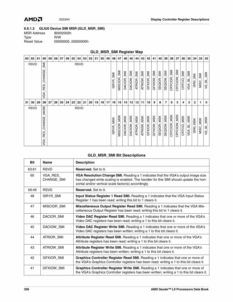
306 AMD Geode™ LX Processors Data Book
Display Controller Register Descriptions33234H
6.6.1.3 GLIU0 Device SMI MSR (GLD_MSR_SMI)MSR Address 80002002hType R/WReset Value 00000000_00000000h
GLD_MSR_SMI Register Map
63 62 61 60 59 58 57 56 55 54 53 52 51 50 49 48 47 46 45 44 43 42 41 40 39 38 37 36 35 34 33 32
RSVD
VG
A_R
ES
_CH
AN
GE
_SM
I
RSVD
ISR
1R_S
MI
MIS
CIO
R_S
MI
DA
CIO
R_S
MI
DA
CIO
W_S
MI
ATR
IOR
_SM
I
ATR
IOW
_SM
I
GF
XIO
R_S
MI
GF
XIO
W_S
MI
SE
QIO
R_S
MI
SE
QIO
W_S
MI
CR
TC
IOR
_SM
I
CR
TC
IOW
_SM
I
CR
TC
IO_S
MI
VG
A_B
L_S
MI
ISR
0_S
MI
MIS
C_S
MI
VG
_BL_
SM
I
31 30 29 28 27 26 25 24 23 22 21 20 19 18 17 16 15 14 13 12 11 10 9 8 7 6 5 4 3 2 1 0
RSVD
VG
A_R
ES
_CH
AN
GE
_MA
SK RSVD
ISR
1R_M
SK
MIS
CIO
R_M
SK
DA
CIO
R_M
SK
DA
CIO
W_M
SK
ATR
IOR
_MS
K
ATR
IOW
_MS
K
GF
XIO
R_M
SK
GF
XIO
W_M
SK
SE
QIO
R_M
SK
SE
QIO
W_M
SK
CR
TC
IOR
_MS
K
CR
TC
IOW
_MS
K
CR
TC
IO_M
SK
VG
A_B
L_M
SK
ISR
0_M
SK
MIS
C_M
SK
VG
_BL_
MS
K
GLD_MSR_SMI Bit Descriptions
Bit Name Description
63:61 RSVD Reserved. Set to 0.
60 VGA_RES_CHANGE_SMI
VGA Resolution Change SMI. Reading a 1 indicates that the VGA’s output image size has changed while scaling is enabled. The handler for this SMI should update the hori-zontal and/or vertical scale factor(s) accordingly.
59:49 RSVD Reserved. Set to 0.
48 ISR1R_SMI Input Status Register 1 Read SMI. Reading a 1 indicates that the VGA Input Status Register 1 has been read; writing this bit to 1 clears it.
47 MISCIOR_SMI Miscellaneous Output Register Read SMI. Reading a 1 indicates that the VGA Mis-cellaneous Output Register has been read; writing this bit to 1 clears it.
46 DACIOR_SMI Video DAC Register Read SMI. Reading a 1 indicates that one or more of the VGA’s Video DAC registers has been read; writing a 1 to this bit clears it.
45 DACIOW_SMI Video DAC Register Write SMI. Reading a 1 indicates that one or more of the VGA’s Video DAC registers has been written; writing a 1 to this bit clears it.
44 ATRIOR_SMI Attribute Register Read SMI. Reading a 1 indicates that one or more of the VGA’s Attribute registers has been read; writing a 1 to this bit clears it.
43 ATRIOW_SMI Attribute Register Write SMI. Reading a 1 indicates that one or more of the VGA’s Attribute registers has been written; writing a 1 to this bit clears it.
42 GFXIOR_SMI Graphics Controller Register Read SMI. Reading a 1 indicates that one or more of the VGA’s Graphics Controller registers has been read; writing a 1 to this bit clears it.
41 GFXIOW_SMI Graphics Controller Register Write SMI. Reading a 1 indicates that one or more of the VGA’s Graphics Controller registers has been written; writing a 1 to this bit clears it.

AMD Geode™ LX Processors Data Book 307
Display Controller Register Descriptions 33234H
40 SEQIOR_SMI Sequencer Register Read SMI. Reading a 1 indicates that one or more of the VGA’s Sequencer registers has been read; writing a 1 to this bit clears it.
39 SEQIOW_SMI Sequencer Register Write SMI. Reading a 1 indicates that one or more of the VGA’s Sequencer registers has been written; writing a 1 to this bit clears it.
38 CRTCIOR_SMI CRTC Register Read SMI. Reading a 1 indicates that one or more of the VGA’s CRTC registers has been read; writing a 1 to this bit clears it.
37 CRTCIOW_SMI CRTC Register Write SMI. Reading a 1 indicates that one or more of the VGA’s CRTC registers has been written; writing a 1 to this bit clears it.
36 CRTCIO_SMI CRTC Invalid Register I/O SMI. Reading a 1 indicates that this SMI has been gener-ated; writing a 1 to this bit clears it; writing 0 has no effect.
35 VGA_BL_SMI VGA Vertical Blank SMI. Reading a 1 indicates that the ASMI corresponding to VGA Vertical Blank has been triggered. Writing a 1 to this bit clears it (and deactivates the ASMI signal); writing a 0 to this bit has no effect.
34 ISR0_SMI Input Status Register 0 SMI. Reading a 1 indicates that a synchronous SMI was gen-erated because of a read to VGA Input Status Register 0. Writing a 1 to this bit clears it; writing a 0 has no effect.
33 MISC_SMI Miscellaneous Output Register SMI. Reading a 1 indicates that a synchronous SMI was generated due to a write to the Miscellaneous Output Register. Writing a 1 to this bit clears it; writing a 0 has no effect.
32 VG_BL_SMI DC Vertical Blank SMI. Reading a 1 indicates that the ASMI corresponding to DC Ver-tical Blank has been triggered. Writing a 1 to this bit clears it (and deactivates the ASMI signal); writing a 0 has no effect.
31:29 RSVD Reserved. Set to 0.
28 VGA_RES_CHANGE_MASK
VGA Resolution Change SMI Mask. When set to 1, disables generation of an asyn-chronous SMI when all of the following conditions occur at once:
- The VGA timing engine is enabled.
- Scaling is enabled.
- The horizontal or vertical resolution of the image produced by the VGA timing engine changes.
27:17 RSVD Reserved. Set to 0.
16 ISR1R_MSK Input Status Register 1 Read SMI Mask. When set to 1, disables generation of the SMI that indicates that VGA Input Status Register 1 has been read.
15 MSICIOR_MSK Miscellaneous Output Register Read SMI. When set to 1, disables generation of the SMI that indicates that the VGA Miscellaneous Output Register has been read.
14 DACIOR_MSK Video DAC Register Read SMI. When set to 1, disables generation of the SMI that indicates that one or more of the VGA’s Video DAC registers has been read.
13 DACIOW_MSK Video DAC Register Write SMI. When set to 1, disables generation of the SMI that indicates that one or more of the VGA’s Video DAC registers has been written.
12 ATRIOR_MSK Attribute Register Read SMI. When set to 1, disables generation of the SMI that indi-cates that one or more of the VGA’s Attribute registers has been read.
11 ATRIOW_MSK Attribute Register Write SMI. When set to 1, disables generation of the SMI that indi-cates that one or more of the VGA’s Attribute registers has been written.
10 GFXIOR_MSK Graphics Controller Register Read SMI. When set to 1, disables generation of the SMI that indicates that one or more of the VGA’s Graphics Controller registers has been read.
GLD_MSR_SMI Bit Descriptions (Continued)
Bit Name Description
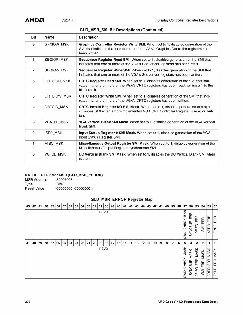
308 AMD Geode™ LX Processors Data Book
Display Controller Register Descriptions33234H
6.6.1.4 GLD Error MSR (GLD_MSR_ERROR)
9 GFXIOW_MSK Graphics Controller Register Write SMI. When set to 1, disables generation of the SMI that indicates that one or more of the VGA’s Graphics Controller registers has been written.
8 SEQIOR_MSK Sequencer Register Read SMI. When set to 1, disables generation of the SMI that indicates that one or more of the VGA’s Sequencer registers has been read.
7 SEQIOW_MSK Sequencer Register Write SMI. When set to 1, disables generation of the SMI that indicates that one or more of the VGA’s Sequencer registers has been written.
6 CRTCIOR_MSK CRTC Register Read SMI. When set to 1, disables generation of the SMI that indi-cates that one or more of the VGA’s CRTC registers has been read; writing a 1 to this bit clears it.
5 CRTCIOW_MSK CRTC Register Write SMI. When set to 1, disables generation of the SMI that indi-cates that one or more of the VGA’s CRTC registers has been written.
4 CRTCIO_MSK CRTC Invalid Register I/O SMI Mask. When set to 1, disables generation of a syn-chronous SMI when a non-implemented VGA CRT Controller Register is read or writ-ten.
3 VGA_BL_MSK VGA Vertical Blank SMI Mask. When set to 1, disables generation of the VGA Vertical Blank SMI.
2 ISR0_MSK Input Status Register 0 SMI Mask. When set to 1, disables generation of the VGA Input Status Register SMI.
1 MISC_MSK Miscellaneous Output Register SMI Mask. When set to 1, disables generation of the Miscellaneous Output Register synchronous SMI.
0 VG_BL_MSK DC Vertical Blank SMI Mask. When set to 1, disables the DC Vertical Blank SMI when set to 1.
MSR Address 80002003hType R/WReset Value 00000000_00000000h
GLD_MSR_SMI Bit Descriptions (Continued)
Bit Name Description
GLD_MSR_ERROR Register Map
63 62 61 60 59 58 57 56 55 54 53 52 51 50 49 48 47 46 45 44 43 42 41 40 39 38 37 36 35 34 33 32
RSVD
CW
D_C
HE
CK
_ER
R
SY
NC
BU
F_E
RR
DF
IFO
_ER
R
SM
I_E
RR
AD
DR
_ER
R
TY
PE
_ER
R
31 30 29 28 27 26 25 24 23 22 21 20 19 18 17 16 15 14 13 12 11 10 9 8 7 6 5 4 3 2 1 0
RSVD
CW
D_C
HE
CK
_MA
SK
SY
NC
BU
F_M
AS
K
DF
IFO
_ER
R_M
AS
K
SM
I_E
RR
_MA
SK
AD
DR
_ER
R_M
AS
K
TY
PE
_ER
R_M
AS
K

AMD Geode™ LX Processors Data Book 309
Display Controller Register Descriptions 33234H
GLD_MSR_ERROR Bit Descriptions
Bit Name Description
63:38 RSVD Reserved. Set to 0.
37 CWD_CHECK_ERR Control Word Check Error. Reading a 1 indicates that an invalid control word was read from the Display FIFO, which is indicative of a FIFO underrun. Writing a 1 to this bit clears it.
36 SYNCBUF_ERR Synchronizer Buffer Error. Reading a 1 indicates that the display pipe attempted to read the synchronizer buffer while it was invalid. This is indicative of a synchronizer buffer underrun. Writing a 1 to this bit clears it.
35 DFIFO_ERR Display FIFO Underrun Error. Reading a 1 indicates that the asynchronous error signal is being driven because the display FIFO has “run dry”. This implies that at least one frame of the display was corrupted. Writing a 1 to this bit clears it; writing a 0 has no effect.
34 SMI_ERR Uncleared SMI Error. Reading a 1 indicates that the asynchronous error signal is being driven because a second SMI occurred while the first SMI went unserviced.
33 ADDR_ERR Unexpected Address Error. Reading a 1 indicates that the exception flag was set because the DC received a GLIU0 transaction request.
32 TYPE_ERR Unexpected Type Error. Reading a 1 indicates that an asynchronous error has occurred because the DC received a GLIU0 transaction with an undefined or unex-pected type.
31:6 RSVD Reserved. Set to 0.
5 CWD_CHECK_MSK Control Word Check Error Mask. When set to 1, disables generation of the asyn-chronous error signal when an invalid control word is read from the data FIFO.
4 SYNCBUF_MSK Synchronizer Buffer Error Mask. When set to 1, disables generation of the asyn-chronous error signal when invalid data is read from the synchronizer buffer.
3 DFIFO_ERR_MASK Display FIFO Underrun Error Mask. When set to 1, disables generation of the asyn-chronous error signal when at least one frame of the display was corrupted.
2 SMI_ERR_MASK Uncleared SMI Error Mask. When set to 1, disables generation of the asynchronous error signal when a second SMI occurred while the first SMI went unserviced.
1 ADDR_ERR_MASK Unexpected Address Error Mask. When set to 1, disables generation of an excep-tion flag when the DC receives a GLIU0 request.
0 TYPE_ERR_MASK Unexpected Type Error Mask. When set to 1, disables generation of the asynchro-nous error signal when the DC received a GLIU0 transaction with an undefined or unexpected type.

310 AMD Geode™ LX Processors Data Book
Display Controller Register Descriptions33234H
6.6.1.5 GLD Power Management MSR (GLD_MSR_PM)
6.6.1.6 GLIU0 Device Diagnostic MSR (GLD_MSR_DIAG)
This register is reserved for internal use by AMD and should not be written to.
MSR Address 80002004hType R/WReset Value 00000000_00000015h
GLD_MSR_PM Register Map
63 62 61 60 59 58 57 56 55 54 53 52 51 50 49 48 47 46 45 44 43 42 41 40 39 38 37 36 35 34 33 32
RSVD
31 30 29 28 27 26 25 24 23 22 21 20 19 18 17 16 15 14 13 12 11 10 9 8 7 6 5 4 3 2 1 0
RSVD
VG
A_G
LCLK
_PM
OD
E
DC
LK_P
MO
DE
GLC
LK_P
MO
DE
GLD_MSR_PM Bit Descriptions
Bit Name Description
63:6 RSVD Reserved. Set to 0.
5:4 VGA_GLCLK_PMODE
VGA GLIU0 Clock Power Management Mode. This field controls the internal clock gating for the GLIU0 clock to the VGA module.
00: Clock is not gated.01: Enable active hardware clock gating. Hardware automatically determines when it is
idle, and internally disables the GLIU0 clock whenever possible.10: Reserved.11: Reserved.
3:2 DCLK_PMODE Dot Clock Power Management Mode. This field controls the internal clock gating for the Dot clock to all logic other than the VGA unit.
00: Clock is not gated.01: Enable active hardware clock gating. Hardware automatically determines when it is
idle, and internally disables the Dot clock whenever possible.10: Reserved.11: Reserved.
1:0 G:CLK_PMODE GLIU0 Clock Power Management Mode. This field controls the internal clock gating for the GLIU0 Clock to all logic other than the VGA unit.
00: Clock is not gated.01: Enable active hardware clock gating. Hardware automatically determines when it is
idle, and internally disables the GLIU0 clock whenever possible.10: Reserved.11: Reserved.
MSR Address 80002005hType R/WReset Value 00000000_00000000h

AMD Geode™ LX Processors Data Book 311
Display Controller Register Descriptions 33234H
6.6.2 Display Controller Specific MSRs
6.6.2.1 SPARE MSR
6.6.2.2 DC RAM Control MSR (DC_RAM_CTL_MSR)
MSR Address 80000011hType R/WReset Value 00000000_00000000h
SPARE_MSR Register Map
63 62 61 60 59 58 57 56 55 54 53 52 51 50 49 48 47 46 45 44 43 42 41 40 39 38 37 36 35 34 33 32
RSVD
31 30 29 28 27 26 25 24 23 22 21 20 19 18 17 16 15 14 13 12 11 10 9 8 7 6 5 4 3 2 1 0
RSVD
DIS
AB
LE_V
FIF
O_W
M RSVD
SPARE_MSR Bit Descriptions
Bit Name Description
63:7 RSVD Reserved.
6 DISABLE_VFIFO_WM
Disable Video FIFO Watermarks. When set, the video watermarks in DC_ARB_CFG[19:12] have no effect.
5:0 RSVD Reserved.
MSR Address 80000012hType R/WReset Value 00000000_02020202h
DC_RAM_CTL_MSR Register Map
63 62 61 60 59 58 57 56 55 54 53 52 51 50 49 48 47 46 45 44 43 42 41 40 39 38 37 36 35 34 33 32
RSVD
31 30 29 28 27 26 25 24 23 22 21 20 19 18 17 16 15 14 13 12 11 10 9 8 7 6 5 4 3 2 1 0
RSVD
CF
IFO
_CT
L RSVD
DV
_RA
M_C
TL
DC_RAM_CTL_MSR Bit Descriptions
Bit Name Description
63:11 RSVD Reserved.
10:8 CFIFO_CTL CFIFO RAM Delay Control.
7:3 RSVD Reserved.
2:0 DV_RAM_CTL DV RAM Delay Control.

312 AMD Geode™ LX Processors Data Book
Display Controller Register Descriptions33234H
6.6.3 Configuration and Status RegistersAll DC registers are DWORD accessible only.
6.6.3.1 DC Unlock (DC_UNLOCK)
This register is provided to lock the most critical memory-mapped DC registers to prevent unwanted modification (writeoperations). Read operations are always allowed.
DC Memory Offset 000hType R/WReset Value 00000000h
DC_UNLOCK Register Map
31 30 29 28 27 26 25 24 23 22 21 20 19 18 17 16 15 14 13 12 11 10 9 8 7 6 5 4 3 2 1 0
RSVD DC_UNLOCK
AMD Geode™ LX Processors Data Book 313
Display Controller Register Descriptions 33234H
DC_UNLOCK Bit Descriptions
Bit Name Description
31:16 RSVD Reserved.
15:0 DC_UNLOCK Unlock Code. This register must be written with the value 4758h in order to write to the protected registers. The following registers are protected by the locking mechanism:
DC_GENERAL_CFG (DC Memory Offset 004h)DC_DISPLAY_CFG (DC Memory Offset 008h)DC_ARB_CFG (DC Memory Offset 00Ch)DC_FB_ST_OFFSET (DC Memory Offset 010h)DC_CB_ST_OFFSET (DC Memory Offset 014h)DC_CURS_ST_OFFSET (DC Memory Offset 018h)DC_VID_Y_ST_OFFSET (DC Memory Offset 020h)DC_VID_U_ST_OFFSET (DC Memory Offset 024h)DC_VID_V_ST_OFFSET (DC Memory Offset 028h)DC_LINE_SIZE (DC Memory Offset 030h)DC_GFX_PITCH (DC Memory Offset 034h)DC_VID_YUV_PITCH (DC Memory Offset 038h)DC_H_ACTIVE_TIMING (DC Memory Offset 040h)DC_H_BLANK_TIMING (DC Memory Offset 044h)DC_H_SYNC_TIMING (DC Memory Offset 048h)DC_V_ACTIVE_TIMING (DC Memory Offset 050h)DC_V_BLANK_TIMING (DC Memory Offset 054h)DC_V_SYNC_TIMING (DC Memory Offset 058h)DC_DFIFO_DIAG (DC Memory Offset 078h)DC_CFIFO_DIAG (DC Memory Offset 07Ch)DC_VID_DS_DELTA (DC Memory Offset 080h)DC_GLIU0_MEM_OFFSET (DC Memory Offset 084h)DC_DV_CTL (DC Memory Offset 088h)DC_GFX_SCALE (DC Memory Offset 090h)DC_IRQ_FILT_CTL (DC Memory Offset 094h)DC_FILT_COEFF1 (DC Memory Offset 098h)DC_FILT_COEFF2 (DC Memory Offset 09Ch)DC_VBI_EVEN_CTL (DC Memory Offset 0A0h)DC_VBI_ODD_CTL (DC Memory Offset 0A4h)DC_VBI_HOR_CTL (DC Memory Offset 0A8h)DC_VBI_LN_ODD (DC Memory Offset 0ACh)DC_VBI_LN_EVEN (DC Memory Offset 0B0h)DC_VBI_PITCH (DC Memory Offset 0B4h)DC_CLR_KEY (DC Memory Offset 0B8h)DC_CLR_KEY_MASK (DC Memory Offset 0BCh)DC_CLR_KEY_X (DC Memory Offset 0C0h)DC_CLR_KEY_Y (DC Memory Offset 0C4h)DC_GENLK_CTL (DC Memory Offset 0D4h)DC_VID_EVEN_Y_ST_OFFSET (DC Memory Offset 0D8h)DC_VID_EVEN_U_ST_OFFSET (DC Memory Offset 0DCh)DC_VID_EVEN_V_ST_OFFSET (DC Memory Offset 0E0h)DC_V_ACTIVE_EVEN_TIMING (DC Memory Offset 0E4h)DC_V_BLANK_EVEN_TIMING (DC Memory Offset 0E8h)DC_V_SYNC_EVEN_TIMING (DC Memory Offset 0ECh)

314 AMD Geode™ LX Processors Data Book
Display Controller Register Descriptions33234H
6.6.3.2 DC General Configuration (DC_GENERAL_CFG)
This register contains general control bits for the DC. Unless otherwise noted in the bit descriptions table, settings written tothis register do not take effect until the start of the following frame or interlaced field.
DC Memory Offset 004hType R/WReset Value 00000000h
DC_GENERAL_CFG Register Map
31 30 29 28 27 26 25 24 23 22 21 20 19 18 17 16 15 14 13 12 11 10 9 8 7 6 5 4 3 2 1 0
DB
UG
DB
SL
CF
RW
DIA
G
CR
C_M
OD
E
SG
FR
SG
RE
SIG
E
SIG
_SE
L
FR
C8P
IX
RS
VD
YU
VM
VD
SE
VG
AF
T
FD
TY
ST
FM
DFHPEL DFHPSL
VG
AE
DE
CE
CM
PE
FIL
T_S
IG_S
EL
VID
E
CLR
_CU
R
CU
RE
DF
LE
DC_GENERAL_CFG Bit Descriptions
Bit Name Description
31 DBUG Debug Mode. Effective immediately.
0: Disable1: Enable.
30 DBSL Debug Select. Effective immediately.
0: FIFO control signals transmitted to debug port.1: Memory control signals transmitted to debug port.
29 CFRW Compressed Line Buffer Read/Write Select. Effective immediately.
Only has effect if in DIAG mode (bit 28 = 1).
0: Write address enabled to Compressed Line Buffer (CLB) in diagnostic mode.1: Read address enabled to CLB in diagnostic mode.
28 DIAG RAM Diagnostic Mode. Effective immediately.
0: Normal operation.1: RAM diagnostic mode. This bit allows testability of the on-chip Display FIFO and CLB
via the diagnostic access registers. A low to high transition resets the Display FIFO and Compressed Line Buffer read and write pointers.
27 CRC_MODE CRC Mode. Effective immediately.
This bit selects the CRC algorithm used to compute the signature.
0: nxt_crc[23:0] <= {crc[22:0], (crc[23], crc[3], crc[2])} ^ data[23:0].1: nxt_crc = (reset) ? 32’h01 :( {crc[30:0], 1’b0} ^ ((crc[31]) ? 32’h04c11db7 : 0) )^ data.
26 SGFR Signature Free Run. Effective immediately.
0: Capture display signature for one frame.1: Capture display signature continuously for multiple frames.
When this bit is cleared, the signature accumulation stops at the end of the current frame.
25 SGRE Signature Read Enable. Effective immediately.
0: Reads to DC_PAL_DATA (DC Memory Offset 074h[23:0]) return palette data.1: Reads to DC_PAL_DATA (DC Memory Offset 074h[23:0]) return signature data. The
palette address register contents are ignored in this case. Note that the automatic pal-ette address increment mechanism will still operate even though the address is ignored.

AMD Geode™ LX Processors Data Book 315
Display Controller Register Descriptions 33234H
24 SIGE Signature Enable. Effective immediately.
0: CRC Signature is reset to 000001h and held (no capture).1: CRC Logic captures the pixel data signature with each pixel clock beginning with the
next leading edge of vertical blank. Note that the CRC Logic treats each 24-bit pixel value as an autonomous 24-bit value (RGB color components are not captured sepa-rately in 8-bit signature registers).
23 SIG_SEL Signature Select. Effective immediately.
1: Causes the CRC signature to be generated based on data being fed into the graphics scaling filter. This data stream does not include border/overscan pixels.
0: Clearing this bit allows bit 4 to select between the CRC calculation at the output of the scaler filter or the CRC signature based on the data being output from the DC, including border/overscan pixels. Also note that the CRC calculation can be affected by the VBI CRC enable bit, located in DC_VBI_EVEN_CTL (DC Memory Offset 0A0h[31]).
22 FRC8PIX Force 8-pixel Character Width. When VGA mode is enabled, setting this bit forces the character width to be 8 pixels, overriding the setting in bit 0 (8-Dot character width) of the VGA’s Sequencer Clocking Mode Register (index 01h). This causes the selection of an 8-pixel character width. This bit should be set for 640x480 flat panels when VGA fixed timing mode is enabled.
21 RSVD Reserved. Always set to 0.
20 YUVM YUV Mode. Selects YUV display mode for video overlay.
0: YUV 4:2:2 display mode.1: YUV 4:2:0 display mode.
19 VDSE Video Downscale Enable.
0: Send all video lines to the display filter.1: Use DC_VID_DS_DELTA (DC Memory Offset 080h[31:18]) as a Digital Differential
Analyzer (DDA) delta value to skip certain video lines to support downscaling in the display filter.
18 VGAFT VGA Fixed Timing. When in VGA mode (VGAE bit 7 = 1), this bit indicates that the GLIU block (DC) timing generator should provide the display timings. The VGA will slave its display activity to the regular DC sync and display enable signals. The VGA image will be centered on the screen, but not scaled to fill the screen. If upscaling is desired, the scaler filter should be used instead of this feature. The final image must have at least six more active lines than the native VGA display settings indicate (i.e., at least three lines of bor-der on the top and bottom of the image).
17 FDTY Frame Dirty Mode.
0: Frame buffer writes mark associated scan line dirty. Used when FB_PITCH (DC Mem-ory Offset 034h[15:0]) is equal to 1 KB, 2 KB, or 4 KB.
1: Frame buffer writes mark entire frame as dirty. Used when FB_PITCH (DC Memory Offset 034h[15:0]) is not equal to 1 KB, 2 KB, or 4 KB.
16 STFM Static Frame Mode. When compression is enabled (CMPE bit 5 = 1), this bit controls the update of dirty scan lines.
0: Update dirty scan lines every frame.1: Update dirty scan lines every other frame.
15:12 DFHPEL Display-FIFO High Priority End Level. This field specifies the depth of the display FIFO (in multiples of 256 bytes) at which a high-priority request previously issued to the mem-ory controller will end. The value is dependent upon display mode. This field should always be non-zero and should be larger than the start level. Note that the settings in the DC_ARB_CFG register (DC Memory Offset 00Ch) can also affect the priority of requests.
DC_GENERAL_CFG Bit Descriptions (Continued)
Bit Name Description

316 AMD Geode™ LX Processors Data Book
Display Controller Register Descriptions33234H
11:8 DFHPSL Display-FIFO High Priority Start Level. This field specifies the depth of the display FIFO (in multiples of 256 bytes) at which a high-priority request is sent to the memory controller to fill up the FIFO. The value is dependent upon display mode. This field should always be non-zero and should be less than the high-priority end level. Note that the set-tings in the DC_ARB_CFG register (DC Memory Offset 00Ch) can also affect the priority of requests.
7 VGAE VGA Enable. When changing the state of this bit, both the DC and VGA should be stopped, and not actively fetching and displaying data.
No other DC features operate with the VGA pass-through feature enabled, with the exception of the CRC/signature feature, the filters, and the timing generator (when the fil-ters or VGA fixed timings are enabled). All other features should be turned off to prevent interference with VGA operation.
0: Normal DC operation.
1: Allow the hardware VGA use of the display FIFO and the memory request interface. The VGA HSYNC, VSYNC, blank, and pixel outputs are routed through the back end of the DC pixel and sync pipeline and then to the I/O pads.
6 DECE Decompression Enable.
0: Disable display refresh decompression.1: Enable display refresh decompression.
5 CMPE Compression Enable.
0: Disable display refresh compression.1: Enable display refresh compression.
4 FILT_SIG_SEL Filter Signature Select. When bit 23 is clear and this bit is set, the CRC mechanism at the output of the scaler filter (before the flicker filter) is enabled. Setting this bit when bit 23 is also set has no effect. When both this bit and bit 23 are cleared, the CRC is taken at the output of the DC, including the border/overscan pixels. Also note that the CRC calcu-lation can be affected by the VBI CRC enable bit, located in DC_VBI_EVEN_CTL (DC Memory Offset 0A0h[31].
3 VIDE Video Enable.
0: Disable video port/overlay.1: Enable video port/overlay.
2 CLR_CUR Color Cursor.
0: 2-bpp format.1: 32-bpp color cursor.
1 CURE Cursor Enable.
0: Disable hardware cursor.1: Enable hardware cursor.
0 DFLE Display-FIFO Load Enable.
0: Disable display FIFO.1: Enable display FIFO. Setting this bit high initiates display refresh requests to the mem-
ory controller at the trailing edge of vertical sync.
DC_GENERAL_CFG Bit Descriptions (Continued)
Bit Name Description

AMD Geode™ LX Processors Data Book 317
Display Controller Register Descriptions 33234H
6.6.3.3 DC Display Configuration (DC_DISPLAY_CFG)
This register contains configuration bits for controlling the various display functions of the DC.
Unless otherwise noted, settings written to this register do not take effect until the start of the following frame or interlacedfield.
DC Memory Offset 008hType R/WReset Value 00000000h
DC_DISPLAY_CFG Register Map
31 30 29 28 27 26 25 24 23 22 21 20 19 18 17 16 15 14 13 12 11 10 9 8 7 6 5 4 3 2 1 0
RSVD
VIS
L
RS
VD
PALB
DC
EN
RSVD VFHPEL VFHPSL
16B
PP
_MO
DE
DIS
P_M
OD
E
RS
VD
TR
UP
RS
VD
VD
EN
GD
EN
RSVD
TG
EN
DC_DISPLAY_CFG Bit Descriptions
Bit Name Description
31:28 RSVD Reserved.
27 VISL Vertical Interrupt Select. Effective immediately.0: SMI generated at start of vertical blank when VIEN is enabled (bit 5 = 1).1: SMI generated at end of vertical sync when VIEN is enabled (bit 5 = 1).
26 RSVD Reserved.
25 PALB PAL Bypass.0: Graphics data is routed through palette RAM in 16, 24, and 32-bpp display modes.1: Graphics data bypasses palette RAM in 16, 24, and 32-bpp display modes. While con-
figured in this mode, 2-bpp cursor and border overlays are supported, but the palette entries for these items must be modified. See Section 6.6.7.1 on page 335 for more information.
24 DCEN Display Center.0: Normal active portion of scan line is qualified with DISPEN (ball AE4).1: Border and active portions of scan line are qualified with DISPEN. This enables cen-
tering the display for flat panels.
23:20 RSVD Reserved.
19:16 VFHPEL Video-FIFO High Priority End Level. This field specifies the depth of the video FIFO (in multiples of 64 bytes) at which a high priority request previously issued to the memory controller for video data will end. This field should always be non-zero and should be larger than the start level. Note that the settings in the DC_ARB_CFG register (DC Mem-ory Offset 00Ch) can also affect the priority of requests. This field should be set to 0 if video overlay is disabled.
15:12 VFHPSL Video-FIFO High Priority Start Level. This field specifies the depth of the video FIFO (in multiples of 64 bytes) at which a high priority request is sent to the memory controller to fill up the video FIFO. This field should always be non-zero and should be less than the high-priority end level. Note that the settings in the DC_ARB_CFG register (DC Memory Offset 00Ch) can also affect the priority of requests.
11:10 16BPP_MODE Per-Pixel Mode. Based on the number of bits per pixel (DISP_MODE bits [9:8] must equal 01), this determines how those bits are allocated to color and alpha information:
For 16-bpp display format:00: 16-bpp (RGB 5:6:5)01: 15-bpp (RGB 5:5:5)10: XRGB (ARGB 4:4:4)11: Reserved

318 AMD Geode™ LX Processors Data Book
Display Controller Register Descriptions33234H
9:8 DISP_MODE Display Mode. Bits per pixel.
00: 8-bpp (also used in VGA emulation)01: 16-bpp10: 24-bpp (RGB 8:8:8)11: 32-bpp
7 RSVD Reserved.
6 TRUP Timing Register Update. Effective immediately.
0: Prevent update of working timing registers. This bit should be set low when a new tim-ing set is being programmed, but the display is still running with the previously pro-grammed timing set.
1: Update working timing registers on next active edge of vertical sync.
5 RSVD Reserved.
4 VDEN Video Data Enable. Set this bit to 1 to allow transfer of video data to the VP.
3 GDEN Graphics Data Enable. Set this bit to 1 to allow transfer of graphics data through the dis-play pipeline.
2:1 RSVD Reserved.
0 TGEN Timing Generator Enable. Effective immediately.
0: Disable timing generator.1: Enable timing generator.
This bit must be set to 0 when using VGA mode unless the filters or VGA Fixed Timings are also enabled (DC_GENERAL_CFG register, bit 18, DC Memory Offset 004h[18]).
DC_DISPLAY_CFG Bit Descriptions (Continued)
Bit Name Description

AMD Geode™ LX Processors Data Book 319
Display Controller Register Descriptions 33234H
6.6.3.4 DC Arbitration Configuration (DC_ARB_CFG)
This register contains configuration bits for controlling the priority level of GLIU requests by the DC. It allows high priority tobe enabled under several conditions (see bits [8:1]). These conditions are ORed with other sources of high-priority, includ-ing the FIFO watermark mechanisms. Settings written to this register take effect immediately. The features in this registerdo not affect the DC’s internal prioritization of video vs. graphics data fetches -- just the priority that is presented on theGeodeLink request. The low priority at VSYNC mechanism (bits [15:9, 0]) takes precedence over all priority mechanismsexcept the high priority when line buffer fill in progress” mechanism bit [1].
DC Memory Offset 00ChType R/WReset Value 00000000h
DC_ARB_CFG Register Map
31 30 29 28 27 26 25 24 23 22 21 20 19 18 17 16 15 14 13 12 11 10 9 8 7 6 5 4 3 2 1 0
RSVDLB
_LO
AD
_WM
_EN
LB_LOAD_WM LPEN_END_COUNT
HP
EN
_SB
_IN
V
HP
EN
_FB
_IN
V_H
ALF
SB
HP
EN
_FB
_IN
V_S
BR
D
HP
EN
_FB
_IN
V
HP
EN
_1LB
_IN
V
HP
EN
_2LB
_IN
V
HP
EN
_3LB
_IN
V
HP
EN
_LB
_FIL
L
LPE
N_V
SY
NC
DC_ARB_CFG Bit Descriptions
Bit Name Description
31:21 RSVD Reserved.
20 LB_LOAD_WM_EN
Line Buffer Load Watermark Enable. When set, allows line buffer loads from the dis-play FIFO to begin when the display FIFO has at least as much data as defined by the watermark in bits [19:16] (LB_LOAD_WM). When this bit is cleared, line buffer loads are not permitted until the display FIFO is full.
19:16 LB_LOAD_WM Line Buffer Load Watermark. When enabled via bit 20 (LB_LOAD_WM_EN), this watermark determines how much data must be in the DFIFO before a line buffer load is permitted. This level is set in 256-byte increments.
15:9 LPEN_END_COUNT
Low Priority End Counter. When bit 0 (LPEN_VSYNC) is set, this field indicates the number of scan lines after VSYNC that the DC will force its requests to low priority. Because the line buffers, flicker filter buffers, sync buffer, and data FIFO are all cleared at VSYNC, this mechanism prevents the DC from spending an inordinate amount of time in high priority while filling all of these buffers. In most cases this value should be set three or four lines less than the distance between VSYNC start and V_TOTAL. This value may need to be lowered if VBI data is enabled.
8 HPEN_SB_INV High Priority Enable when Sync Buffer Invalid. This bit enables the DC to arbitrate in high priority whenever the synchronizer buffer does not contain valid data.
7 HPEN_FB_INV_HALFSB
High Priority Enable when Flicker Buffer invalid and Sync Buffer less than Half Full. This bit enables the DC to arbitrate in high priority whenever the synchronizer buffer is less than half full and the flicker filter buffer does not contain valid data.
6 HPEN_FB_INV_SBRD
High Priority Enable when Flicker Buffer invalid and Sync Buffer Being Read. This bit enables the DC to arbitrate in high priority whenever the synchronizer buffer is being read and the flicker filter buffer does not contain valid data.
5 HPEN_FB_INV High Priority Enable when Flicker Buffer Invalid. This bit enables the DC to arbitrate at high priority whenever the flicker filter buffer does not contain valid data.
4 HPEN_1LB_INV High Priority Enable when Any One Line Buffer Invalid. This bit enables the DC to arbitrate at high priority if any of the three line buffers is invalid. (When the scaler filter is disabled, only one logical line buffer is used, and the state of the others is ignored.)

320 AMD Geode™ LX Processors Data Book
Display Controller Register Descriptions33234H
3 HPEN_2LB_INV High Priority Enable when Any Two Line Buffers Invalid. This bit enables the DC to arbitrate at high priority if the scaler filter is enabled and any two of the three line buffers that feed this filter are invalid. (The state of this bit is ignored if the scaler filter is dis-abled.)
2 HPEN_3LB_INV High Priority Enable when Any Three Line Buffers Invalid. This bit enables the DC to arbitrate at high priority if the scaler filter is enabled and all of the three line buffers that feed this filter are invalid. (The state of this bit is ignored if the scaler filter is disabled.)
1 HPEN_LB_FILL High Priority Enable when Line Buffer Fill in Progress. This bit enables the DC to maintain high priority requests whenever it is in the process of filling a line buffer. The line buffer fill requires an entire scan line of data to be read from the data FIFO without inter-ruption. Because the FIFO typically does not contain a full scan line of data, it is neces-sary to fetch additional data from memory during this process.
0 LPEN_VSYNC Low Priority Enable at VSYNC. When this bit is set, the DC is forced to arbitrate at low priority for a number of lines after the start of VSYNC. (This number of lines is pro-grammed in bits [15:9] (LPEN_END_COUNT)) Because the line buffers, flicker filter buff-ers, sync buffer, and data FIFO are all cleared at VSYNC, this mechanism prevents the DC from spending an inordinate amount of time in high priority while filling all of these buffers.
In most cases this value should be set three or four lines less than the distance between VSYNC start and V_TOTAL This value may need to be lowered if VBI data is enabled.
During this low priority period after VSYNC, this mechanism overrides the watermark mechanism for the data FIFO and all of the other mechanisms in this register except the high priority enable when line buffer fill in progress mechanism enabled in bit 1 (HPEN_LB_FILL). Outside of this period, this mechanism has no effect on the priority level of outgoing DC requests on the GLIU.
DC_ARB_CFG Bit Descriptions (Continued)
Bit Name Description

AMD Geode™ LX Processors Data Book 321
Display Controller Register Descriptions 33234H
6.6.4 Memory Organization RegistersThe graphics memory region is up to 16 MB in size. The graphics memory is made up of the normal uncompressed framebuffer, compressed display buffer, cursor buffer, cursor color buffer (for 16-bit color cursor), and video buffer(s). Each bufferbegins at a programmable offset within the graphics memory region.
The various memory buffers are arranged so as to efficiently pack the data within the graphics memory region. Thisrequires flexibility in the way that the buffers are arranged when different display modes are in use. The cursor and cursorcolor buffers are linear blocks, so addressing is straightforward. The frame buffer and compressed display buffer arearranged based upon scan lines. Each scan line has a maximum number of valid or active QWORDs and a pitch that, whenadded to the previous line offset, points to the next line. In this way, the buffers may be stored as linear blocks or as rectan-gular blocks.
The various buffers’ addresses are all located within the same 1 MB-aligned region. Thus, a separate register,DC_GLIU0_MEM_OFFSET (DC Memory Offset 084h), is used to set a 1 MB-aligned base address.
GART address translation is not supported.
6.6.4.1 DC Frame Buffer Start Address (DC_FB_ST_OFFSET)
This register specifies the offset at which the frame buffer starts. Settings written to this register do not take effect until thestart of the following frame or interlaced field.
DC Memory Offset 010hType R/WReset Value xxxxxxxxh
DC_FB_ST_OFFSET
31 30 29 28 27 26 25 24 23 22 21 20 19 18 17 16 15 14 13 12 11 10 9 8 7 6 5 4 3 2 1 0
RSVD OFFSET
DC_FB_ST_OFFSET Bit Descriptions
Bit Name Description
31:28 RSVD Reserved.
27:0 OFFSET Frame Buffer Start Offset. This value represents the byte offset of the starting location of the displayed frame buffer. This value may be changed to achieve panning across a virtual desktop or to allow multiple buffering.
When this register is programmed to a non-zero value, the compression logic should be disabled. The memory address defined by bits [27:3] takes effect at the start of the next frame scan. The pixel offset defined by bits [2:0] is latched at the end of vertical sync and added to the pixel panning offset to determine the actual panning value.

322 AMD Geode™ LX Processors Data Book
Display Controller Register Descriptions33234H
6.6.4.2 DC Compression Buffer Start Address (DC_CB_ST_OFFSET)
This register specifies the offset at which the compressed display buffer starts. Settings written to this register do not takeeffect until the start of the following frame or interlaced field.
6.6.4.3 DC Cursor Buffer Start Address (DC_CURS_ST_OFFSET)
This register specifies the offset at which the cursor memory buffer starts. Settings written to this register do not take effectuntil the start of the following frame or interlaced field.
DC Memory Offset 014hType R/WReset Value xxxxxxxxh
DC_CB_ST_OFFSET Register Map
31 30 29 28 27 26 25 24 23 22 21 20 19 18 17 16 15 14 13 12 11 10 9 8 7 6 5 4 3 2 1 0
RSVD OFFSET 0h
DC_CB_ST_OFFSET Bit Descriptions
Bit Name Description
31:28 RSVD Reserved.
27:0 OFFSET Compressed Display Buffer Start Offset. This value represents the byte offset of the starting location of the compressed display buffer. The lower five bits should always be programmed to zero so that the start offset is aligned to a 32-byte boundary. This value should change only when a new display mode is set due to a change in size of the frame buffer.
DC Memory Offset 018hType R/WReset Value xxxxxxxxh
DC_CURS_ST_OFFSET Register Map
31 30 29 28 27 26 25 24 23 22 21 20 19 18 17 16 15 14 13 12 11 10 9 8 7 6 5 4 3 2 1 0
RSVD OFFSET 0h
DC_CURS_ST_OFFSET Bit Descriptions
Bit Name Description
31:28 RSVD Reserved.
27:0 OFFSET Cursor Start Offset. This value represents the byte offset of the starting location of the cursor display pattern. The lower five bits should always be programmed to zero so that the start offset is 32-byte aligned. Note that if there is a Y offset for the cursor pattern, the cursor start offset should be set to point to the first displayed line of the cursor pattern.

AMD Geode™ LX Processors Data Book 323
Display Controller Register Descriptions 33234H
6.6.4.4 DC Video Y Buffer Start Address Offset (DC_VID_Y_ST_OFFSET)
This register specifies the offset at which the video Y (YUV 4:2:0) or YUV (YUV 4:2:2) buffer starts.
The upper 4 bits of this register are for the field count mechanism. This mechanism, which did not exist on previousAMD Geode processors, allows the DC to fetch multiple fields or frames of VIP data without requiring software interventionto move the offset. This mechanism has the constraint that the buffers for multiple video frames must be contiguous inmemory. (The VIP hardware will meet this constraint.)
Settings written to this register do not take effect until the start of the following frame or interlaced field.
6.6.4.5 DC Video U Buffer Start Address Offset (DC_VID_U_ST_OFFSET)
This register specifies the offset at which the video U (YUV 4:2:0) buffer starts.
Settings written to this register do not take effect until the start of the following frame or interlaced field.
DC Memory Offset 020hType R/WReset Value xxxxxxxxh
DC_VID_Y_ST_OFFSET Register Map
31 30 29 28 27 26 25 24 23 22 21 20 19 18 17 16 15 14 13 12 11 10 9 8 7 6 5 4 3 2 1 0
RSVD OFFSET 0h
DC_VID_Y_ST_OFFSET Bit Descriptions
Bit Name Description
31:28 RSVD Reserved. Reserved for field count mechanism
27:0 OFFSET Video Y Buffer Start Offset. This value represents the starting location for Video Y Buffer. The lower five bits should always be programmed as zero so that the start offset is aligned to a 32-byte boundary. If YUV 4:2:2 mode is selected (DC Memory Offset 004h[20] = 0), the Video Y Buffer is used as a singular buffer holding interleaved Y, U and V data. If YUV 4:2:0 is selected (DC Memory Offset 004h[20] = 1), the Video Y Buffer is used to hold only Y data while U and V data are stored in separate buffers whose start offsets are represented in DC_VID_U_ST_OFFSET (DC Memory Offset 024h[27:0]) and DC_VID_V_ST_OFFSET (DC Memory Offset 028h[27:0]).
DC Memory Offset 024hType R/WReset Value xxxxxxxxh
DC_VID_U_ST_OFFSET Register Map
31 30 29 28 27 26 25 24 23 22 21 20 19 18 17 16 15 14 13 12 11 10 9 8 7 6 5 4 3 2 1 0
FRAME_COUNT OFFSET 0

324 AMD Geode™ LX Processors Data Book
Display Controller Register Descriptions33234H
6.6.4.6 DC Video V Buffer Start Address Offset (DC_VID_V_ST_OFFSET)
This register specifies the offset at which the video V buffer starts.
Settings written to this register do not take effect until the start of the following frame or interlaced field.
6.6.4.7 DC Dirty/Valid Region Top (DC_DV_TOP)
This register specifies the top of the frame buffer memory region to be watched for frame-dirty mode.
Settings written to this register take effect immediately.
DC_VID_U_ST_OFFSET Bit Descriptions
Bit Name Description
31:28 FRAME_COUNT Frame Count. When reading this register, this field indicates the current frame count, as determined by counting rising edges of VIP VSYNC. This value is reset to 0 when VIP_VSYNC occurs and FRAME_CNT >= FRAME_LIMIT. It can also be written to pro-vide a mechanism for software to synchronize activities between the VIP and the Dis-play Controller. However, this can result in corrupted video data until the next reset of this counter.
27:0 OFFSET Video U Buffer Start Offset. This value represents the starting location for the Video U Buffer. The lower three bits should always be programmed as zero so that the start off-set is aligned to a QWORD boundary. A buffer for U data is only used if YUV 4:2:0 dis-play mode is selected (DC Memory Offset 004h[20] = 1).
DC Memory Offset 028hType R/WReset Value xxxxxxxxh
DC_VID_V_ST_OFFSET Register Map
31 30 29 28 27 26 25 24 23 22 21 20 19 18 17 16 15 14 13 12 11 10 9 8 7 6 5 4 3 2 1 0
RSVD OFFSET 0
DC_VID_V_ST_OFFSET Bit Descriptions
Bit Name Description
31:28 RSVD Reserved.
27:0 OFFSET Video V Buffer Start Offset. This value represents the starting location for the Video V Buffer. The lower three bits should always be programmed as zero so that the start offset is aligned to a QWORD boundary. A buffer for V data is only used if YUV 4:2:0 display mode is selected (DC Memory Offset 004h[20] = 1).
DC Memory Offset 02ChType R/WReset Value 00000000h
DC_DV_TOP Register Map
31 30 29 28 27 26 25 24 23 22 21 20 19 18 17 16 15 14 13 12 11 10 9 8 7 6 5 4 3 2 1 0
RSVD DV_TOP RSVD
DV
_TO
P_E
N

AMD Geode™ LX Processors Data Book 325
Display Controller Register Descriptions 33234H
6.6.4.8 DC Line Size (DC_LINE_SIZE)
This register specifies the number of bytes to transfer for a line of frame buffer, compression buffer, and video buffer data.The compressed line buffer is invalidated if it exceeds the CB_LINE_SIZE (bits [18:12]).
Settings written to this register do not take effect until the start of the following frame or interlaced field.
DC_DV_TOP Bit Descriptions
Bit Name Description
31:24 RSVD Reserved. These bits should be programmed to zero.
23:10 DV_TOP_ADDR Dirty/Valid Region Top Address. When enabled via bit 0 (DV_TOP_EN), this field indi-cates the size of the region to be watched for frame buffer accesses. When writes to this region occur and the compression logic is in frame-dirty mode, the frame is marked as dirty. (Writes outside this region, regardless of the settings in the DV_CTL register (DC Memory Offset 088h), do not cause the frame to be marked as dirty in frame-dirty mode.) The bits in this field correspond to address bits [23:10].
9:1 RSVD Reserved. These bits should be programmed to zero.
0 DV_TOP_EN Dirty/Valid Region Top Enable. This bit enables the top-of-region check for frame-dirty mode. This bit should be cleared if the compression logic is NOT configured for frame-dirty mode.
DC Memory Offset 030hType R/WReset Value xxxxxxxxh
DC_LINE_SIZE Register Map
31 30 29 28 27 26 25 24 23 22 21 20 19 18 17 16 15 14 13 12 11 10 9 8 7 6 5 4 3 2 1 0
RSVD VID_LINE_SIZE
RS
VD CB_LINE_SIZE RSVD FB_LINE_SIZE
DC_LINE_SIZE Bit Descriptions
Bit Name Description
31:30 RSVD Reserved. These bits should be programmed to zero.
29:20 VID_LINE_SIZE Video Line Size. This value specifies the number of QWORDs (8-byte segments) to transfer for each source line from the video buffer in YUV 4:2:2 mode. In YUV 4:2:0 mode, it specifies the number of QWORDs to transfer for the U or V stream for a source line (2x this amount is transferred for the Y stream). In YUV 4:2:2 mode, this field must be set to a multiple of four QWORDs -- bits [21:20] must be 0.
19 RSVD Reserved. This bit should be programmed to zero.
18:12 CB_LINE_SIZE Compressed Display Buffer Line Size. This value represents the number of QWORDs for a valid compressed line plus 1. It is used to detect an overflow of the compressed data FIFO. When the compression data for a line reaches CB_LINE_SIZE QWORDs, the line is deemed incompressible. Note that DC actually writes CB_LINE_SIZE + 4 QWORDs to memory, so if X QWORDs are allocated for each compression line, then X - 4 + 1 (or X - 3) should be programmed into this register. Note also that the CB_LINE_SIZE field should never be larger than 65 (041h) since the maximum size of the compressed data FIFO is 64 QWORDs.
11:10 RSVD Reserved. These bits should be programmed to zero.
9:0 FB_LINE_SIZE Frame Buffer Line Size. This value specifies the number of QWORDs (8-byte seg-ments) to transfer for each display line from the frame buffer.

326 AMD Geode™ LX Processors Data Book
Display Controller Register Descriptions33234H
6.6.4.9 DC Graphics Pitch (DC_GFX_PITCH)
This register stores the pitch for the graphics display buffers.
6.6.4.10 DC Video YUV Pitch (DC_VID_YUV_PITCH)
This register stores the pitch for the video buffers.
DC Memory Offset 034hType R/WReset Value xxxxxxxxh
DC_GFX_PITCH Register Map
31 30 29 28 27 26 25 24 23 22 21 20 19 18 17 16 15 14 13 12 11 10 9 8 7 6 5 4 3 2 1 0
CB_PITCH FB_PITCH
DC_GFX_PITCH Bit Descriptions
Bit Name Description
31:16 CB_PITCH Compressed Display Buffer Pitch. This value represents the number of QWORDs between consecutive scan lines of compressed buffer data in memory. This pitch must be set to a multiple of four QWORDs (i.e., bits [17:16] must be 00).
15:0 FB_PITCH Frame Buffer Pitch. This value represents the number of QWORDs between consecu-tive scan lines of frame buffer data in memory.
DC Memory Offset 038hType R/WReset Value xxxxxxxxh
DC_VID_YUV_PITCH Register Map
31 30 29 28 27 26 25 24 23 22 21 20 19 18 17 16 15 14 13 12 11 10 9 8 7 6 5 4 3 2 1 0
UV_PITCH Y_PITCH
DC_VID_YUV_PITCH Bit Descriptions
Bit Name Description
31:16 UV_PITCH Video U and V Buffer Pitch. This value represents the number of QWORDs between consecutive scan lines of U or V buffer data in memory. (U and V video buffers are always the same pitch.) A pitch up to 512 KB is supported to allow for vertical decimation for downscaling.
15:0 Y_PITCH Video Y Buffer Pitch. This value represents the number of QWORDs between consecu-tive scan lines of Y buffer data in memory. A pitch up to 512 KB is supported to allow for vertical decimation for downscaling.

AMD Geode™ LX Processors Data Book 327
Display Controller Register Descriptions 33234H
6.6.5 Timing RegistersThe DC timing registers control the generation of sync, blanking, and active display regions. These registers are generallyprogrammed by the BIOS from an INT 10h call or by the extended mode driver from a display timing file.
Example: To display a 1024x768 graphics (frame buffer) image on a 720x483/59.94 television. The DC CRTC settings areas follows:
Note: The above timings are based on tables B.1 and B.2 in the ANSI/SMTPE 293M-1996 spec. They assume that theframe buffer image should be displayed over the entire 720x483 screen, with no additional border.
The DC_GFX_SCALE (DC Memory Offset 090h) register would be set up to scale the 1024x768 image to a 720x483frame:
v_scale = (768/(483-1)) = 1.593360995...
h_scale = (1024/(720 - 1)) = 1.424200278...
DC_GFX_SCALE = 65F9_5B26h (v_scale = 1.593322754; h_scale = 1.424194336)
In addition, the FILT_ENA and INTL_EN bits would be set (DC Memory Offset 94h[12,11] = 11), and the filter coefficientswould be programmed. This example also presumes that the FLICK_EN bit is set (DC Memory Offset 0D4h[24] = 1).
Because the output is to be interlaced, the flicker filter can be used. (Use of the flicker filter is not required.) For informationon the configuration bits for the flicker filter, see "DC GenLock Control (DC_GENLK_CTL)" on page 350.
DC_H_ACTIVE_TIMING (040h) = 0x035A_02D0 // h_total = 858; h_active = 720
DC_H_BLANK_TIMING (044h) = 0x35A_02D0 // h_blank_start = 720; h_blank_end=858 -- no overscan
DC_H_SYNC_TIMING (048h) = 0x031F_02E0 // h_sync start = 736; h_sync_end = 799
DC_V_ACTIVE_TIMING (050h) = 0x0106_00F1 // v_total = 262 (even) 263(odd); v_active = 241 (even & odd)
DC_V_BLANK_TIMING (054h) = 0x0106_00F1 // v_blank_start = 241; v_blank_end = 262 -- no overscan
DC_V_SYNC_TIMING (058h) = 0x00F6_00F5 // v_sync_start = 245; vsync_end = 246
DC_V_ACTIVE_EVEN_TIMING (0E4h) = 0x0105_00F0
// v_total = 261; v_active = 240
DC_V_BLANK_EVEN_TIMING (0E8h) = 0x0105_00F0
// v_blank_start = 240; v_blank_end = 261
DC_V_SYNC_EVEN_TIMING (0ECh) = 0x00F6_00F5 // v_sync_start = 245; v_sync_end = 246
DC_B_ACTIVE (05Ch) = 03FF_02FFh // frame buffer size1024x768

328 AMD Geode™ LX Processors Data Book
Display Controller Register Descriptions33234H
6.6.5.1 DC Horizontal and Total Timing (DC_H_ACTIVE_TIMING)
This register contains horizontal active and total timing information.
DC Memory Offset 040hType R/WReset Value xxxxxxxxh
DC_H_ACTIVE_TIMING Register Map
31 30 29 28 27 26 25 24 23 22 21 20 19 18 17 16 15 14 13 12 11 10 9 8 7 6 5 4 3 2 1 0
RSVD H_TOTAL RSVD H_ACTIVE
DC_H_ACTIVE_TIMING Bit Descriptions
Bit Name Description
31:28 RSVD Reserved. These bits should be programmed to zero.
27:16 H_TOTAL Horizontal Total. This field represents the total number of pixel clocks for a given scan line minus 1. Note that the value must represent a value greater than the H_ACTIVE field (bits [11:0]) because it includes border pixels and blanked pixels. For flat panels, this value will never change. Unlike previous versions of the DC, the horizontal total can be programmed to any pixel granularity; it is not limited to character (8-pixel) granularity.
15:12 RSVD Reserved. These bits should be programmed to zero.
11:0 H_ACTIVE Horizontal Active. This field represents the total number of pixel clocks for the displayed portion of a scan line minus 1. Note that for flat panels, if this value is less than the panel active horizontal resolution (H_PANEL), the parameters H_BLK_START, H_BLK_END (DC Memory Offset 044h[11:0, 27:16]), H_SYNC_ST, and H_SYNC_END (DC Memory Offset 048h[11:0, 27:16]) should be reduced by the value of H_ADJUST (or the value of H_PANEL - H_ACTIVE / 2) to achieve horizontal centering.
Unlike previous versions of the DC, this field can be programmed to any pixel granularity; it is not limited to character (8-pixel) granularity.
If graphics scaling is enabled, this value represents the width of the final (scaled) image to be displayed. The width of the frame buffer image may be different in this case; DC_FB_ACTIVE (DC Memory Offset 05Ch) is used to program the horizontal and verti-cal active values in the frame buffer when graphics scaling is enabled.
H_ACTIVE must be set to at least 64 pixels.
AMD Geode™ LX Processors Data Book 329
Display Controller Register Descriptions 33234H
6.6.5.2 DC CRT Horizontal Blanking Timing (DC_H_BLANK_TIMING)
This register contains CRT horizontal blank timing information.
Note: A minimum of 32 pixel clocks is required for the horizontal blanking portion of a line in order for the timing generatorto function correctly.
6.6.5.3 DC CRT Horizontal Sync Timing (DC_H_SYNC_TIMING)
This register contains CRT horizontal sync timing information. Note however, that this register should also be programmedappropriately for flat panel only display, since the horizontal sync transition determines when to advance the verticalcounter.
DC Memory Offset 044hType R/WReset Value xxxxxxxxh
DC_H_BLANK_TIMING Register Map
31 30 29 28 27 26 25 24 23 22 21 20 19 18 17 16 15 14 13 12 11 10 9 8 7 6 5 4 3 2 1 0
RSVD H_BLK_END RSVD H_BLK_START
DC_H_BLANK_TIMING Bit Descriptions
Bit Name Description
31:28 RSVD Reserved. These bits should be programmed to zero.
27:16 H_BLK_END Horizontal Blank End. This field represents the pixel clock count at which the horizontal blanking signal becomes inactive minus 1.
Unlike previous versions of the DC, this field can be programmed to any pixel granularity; it is not limited to character (8-pixel) granularity.
15:12 RSVD Reserved. These bits should be programmed to zero.
11:0 H_BLK_START Horizontal Blank Start. This field represents the pixel clock count at which the horizon-tal blanking signal becomes active minus 1.
Unlike previous versions of the DC, this field can be programmed to any pixel granularity; it is not limited to character (8-pixel) granularity.
DC Memory Offset 048hType R/WReset Value xxxxxxxxh
DC_H_SYNC_TIMING Register Map
31 30 29 28 27 26 25 24 23 22 21 20 19 18 17 16 15 14 13 12 11 10 9 8 7 6 5 4 3 2 1 0
RSVD H_SYNC_END RSVD H_SYNC_ST
DC_H_SYNC_TIMING Bit Descriptions
Bit Name Description
31:28 RSVD Reserved. These bits should be programmed to zero.
27:16 H_SYNC_END Horizontal Sync End. This field represents the pixel clock count at which the CRT hori-zontal sync signal becomes inactive minus 1.
Unlike previous versions of the DC, this field can be programmed to any pixel granularity; it is not limited to character (8-pixel) granularity.
The horizontal sync must be at least 8 pixels in width.

330 AMD Geode™ LX Processors Data Book
Display Controller Register Descriptions33234H
6.6.5.4 DC Vertical and Total Timing (DC_V_ACTIVE_TIMING)
This register contains vertical active and total timing information. The parameters pertain to both CRT and flat panel display.All values are specified in lines.
15:12 RSVD Reserved. These bits should be programmed to zero.
11:0 H_SYNC_ST Horizontal Sync Start. This field represents the pixel clock count at which the CRT hori-zontal sync signal becomes active minus 1.
Unlike previous versions of the DC, this field can be programmed to any pixel granularity; it is not limited to character (8-pixel) granularity.
The horizontal sync must be at least 8 pixels in width, and cannot begin until at least 8 pixels after H_BLK_START (DC Memory Offset 044h[11:0]).
DC Memory Offset 050hType R/WReset Value xxxxxxxxh
DC_H_SYNC_TIMING Bit Descriptions
Bit Name Description
DC_V_ACTIVE_TIMING Register Map
31 30 29 28 27 26 25 24 23 22 21 20 19 18 17 16 15 14 13 12 11 10 9 8 7 6 5 4 3 2 1 0
RSVD V_TOTAL RSVD V_ACTIVE
DC_V_ACTIVE_TIMING Bit Descriptions
Bit Name Description
31:27 RSVD Reserved. These bits should be programmed to zero.
26:16 V_TOTAL Vertical Total. This field represents the total number of lines for a given frame scan minus 1. Note that the value is necessarily greater than the V_ACTIVE field (bits [10:0]) because it includes border lines and blanked lines. If the display is interlaced, the total number of lines must be odd, so this value should be an even number.
15:11 RSVD Reserved. These bits should be programmed to zero.
10:0 V_ACTIVE Vertical Active. This field represents the total number of lines for the displayed portion of a frame scan minus 1. Note that for flat panels, if this value is less than the panel active vertical resolution (V_PANEL), the parameters V_BLANK_START, V_BLANK_END (DC Memory Offset 054h[10:0, 26:16]), V_SYNC_START, and V_SYNC_END (DC Memory Offset 058h[10:0, 26:16]) should be reduced by the following value (V_ADJUST) to achieve vertical centering:
V_ADJUST = (V_PANEL - V_ACTIVE) / 2
If the display is interlaced, the number of active lines should be even, so this value should be an odd number.
If graphics scaling is enabled (and interleaved display is disabled), this value represents the height of the final (scaled) image to be displayed. The height of the frame buffer image may be different in this case; DC_FB_ACTIVE (DC Memory Offset 05Ch) is used to program the horizontal and vertical active values in the frame buffer when graphics scaling is enabled.
If interleaved mode is enabled, this value represents half the height of the final (scaled and interleaved) displayed image.

AMD Geode™ LX Processors Data Book 331
Display Controller Register Descriptions 33234H
6.6.5.5 DC CRT Vertical Blank Timing (DC_V_BLANK_TIMING)
This register contains vertical blank timing information. All values are specified in lines. For interlaced display, no border issupported, so blank timing is implied by the total/active timing.
6.6.5.6 DC CRT Vertical Sync Timing (DC_V_SYNC_TIMING)
This register contains CRT vertical sync timing information. All values are specified in lines.
DC Memory Offset 054hType R/WReset Value xxxxxxxxh
DC_V_BLANK_TIMING Register Map
31 30 29 28 27 26 25 24 23 22 21 20 19 18 17 16 15 14 13 12 11 10 9 8 7 6 5 4 3 2 1 0
RSVD V_BLANK_END RSVD V_BLANK_START
DC_V_BLANK_TIMING Bit Descriptions
Bit Name Description
31:27 RSVD Reserved. These bits should be programmed to zero.
26:16 V_BLANK_END Vertical Blank End. This field represents the line at which the vertical blanking signal becomes inactive minus 1. If the display is interlaced, no border is supported, so this value should be identical to V_TOTAL.
15:11 RSVD Reserved. These bits should be programmed to zero.
10:0 V_BLANK_START
Vertical Blank Start. This field represents the line at which the vertical blanking signal becomes active minus 1. If the display is interlaced, this value should be programmed to V_ACTIVE plus 1.
DC Memory Offset 058hType R/WReset Value xxxxxxxxh
DC_V_SYNC_TIMING Register Map
31 30 29 28 27 26 25 24 23 22 21 20 19 18 17 16 15 14 13 12 11 10 9 8 7 6 5 4 3 2 1 0
RSVD V_SYNC_END RSVD V_SYNC_START
DC_V_SYNC_TIMING Bit Descriptions
Bit Name Description
31:27 RSVD Reserved. These bits should be programmed to zero.
26:16 V_SYNC_END Vertical Sync End. This field represents the line at which the CRT vertical sync signal becomes inactive minus 1.
15:11 RSVD Reserved. These bits should be programmed to zero.
10:0 V_SYNC_START
Vertical Sync Start. This field represents the line at which the CRT vertical sync signal becomes active minus 1. For interlaced display, note that the vertical counter is incre-mented twice during each line and since there are an odd number of lines, the vertical sync pulse will trigger in the middle of a line for one field and at the end of a line for the subsequent field.

332 AMD Geode™ LX Processors Data Book
Display Controller Register Descriptions33234H
6.6.5.7 DC Frame Buffer Active Region Register (DC_FB_ACTIVE)
6.6.6 Cursor Position and Line Count/Status RegistersThe cursor registers contain pixel coordinate information for the cursor. These values are not latched by the timing genera-tor until the start of the frame to avoid tearing artifacts when moving the cursor.
The Line Count/Status register holds status information for the current display status, including the current scan line for thedisplay.
6.6.6.1 DC Cursor X Position (DC_CURSOR_X)
This register contains the X position information of the hardware cursor.
Settings written to this register do not take effect until the start of the following frame or interlaced field.
DC Memory Offset 05ChType R/WReset Value xxxxxxxxh
DC_FB_ACTIVE Register Map
31 30 29 28 27 26 25 24 23 22 21 20 19 18 17 16 15 14 13 12 11 10 9 8 7 6 5 4 3 2 1 0
FB_H_ACTIVE FB_V_ACTIVE
DC_FB_ACTIVE Bit Descriptions
Bit Name Description
31:16 FB_H_ACTIVE Horizontal Frame Buffer Active End. This field is used only when graphics scaling is enabled. The lower three bits of this register are ignored and presumed to be 111. Includ-ing these bits, the value in this field represents the total number of pixels in a line in the graphics frame buffer minus 1.
This field is analogous to the H_ACTIVE field in the DC_H_ACTIVE_TIMING register (DC Memory Offset 040h[11:0]), except that this field is used only for the fetching and rendering of pixel data, not the display timings. When graphics scaling is disabled, this field is not used. (The H_ACTIVE field is used instead.
15:0 FB_V_ACTIVE Vertical Frame Buffer Active. This field is used only when graphics scaling is enabled. It represents the total number of lines in the graphics frame buffer minus 1.
This field is analogous to the V_ACTIVE field in the DC_V_ACTIVE_TIMING register (DC Memory Offset 050h[10:0]), except that this field is used only for the fetching and render-ing of pixel data, not the display timings. When graphics scaling is disabled, this field is not used. (The V_ACTIVE field is used instead.)
DC Memory Offset 060hType R/WReset Value xxxxxxxxh
DC_CURSOR_X Register Map
31 30 29 28 27 26 25 24 23 22 21 20 19 18 17 16 15 14 13 12 11 10 9 8 7 6 5 4 3 2 1 0
RSVD X_OFFSET CURSOR_X
DC_CURSOR_X Bit Descriptions
Bit Name Description
31:17 RSVD Reserved.
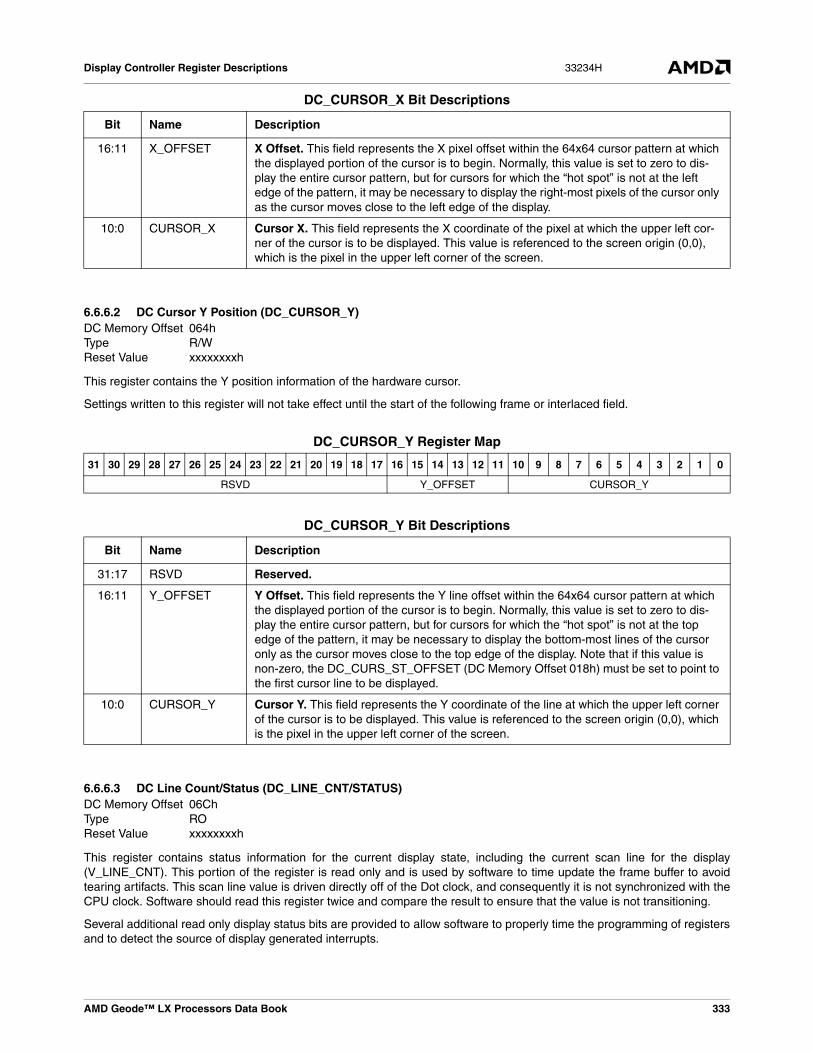
AMD Geode™ LX Processors Data Book 333
Display Controller Register Descriptions 33234H
6.6.6.2 DC Cursor Y Position (DC_CURSOR_Y)
This register contains the Y position information of the hardware cursor.
Settings written to this register will not take effect until the start of the following frame or interlaced field.
6.6.6.3 DC Line Count/Status (DC_LINE_CNT/STATUS)
This register contains status information for the current display state, including the current scan line for the display(V_LINE_CNT). This portion of the register is read only and is used by software to time update the frame buffer to avoidtearing artifacts. This scan line value is driven directly off of the Dot clock, and consequently it is not synchronized with theCPU clock. Software should read this register twice and compare the result to ensure that the value is not transitioning.
Several additional read only display status bits are provided to allow software to properly time the programming of registersand to detect the source of display generated interrupts.
16:11 X_OFFSET X Offset. This field represents the X pixel offset within the 64x64 cursor pattern at which the displayed portion of the cursor is to begin. Normally, this value is set to zero to dis-play the entire cursor pattern, but for cursors for which the “hot spot” is not at the left edge of the pattern, it may be necessary to display the right-most pixels of the cursor only as the cursor moves close to the left edge of the display.
10:0 CURSOR_X Cursor X. This field represents the X coordinate of the pixel at which the upper left cor-ner of the cursor is to be displayed. This value is referenced to the screen origin (0,0), which is the pixel in the upper left corner of the screen.
DC Memory Offset 064hType R/WReset Value xxxxxxxxh
DC_CURSOR_X Bit Descriptions
Bit Name Description
DC_CURSOR_Y Register Map
31 30 29 28 27 26 25 24 23 22 21 20 19 18 17 16 15 14 13 12 11 10 9 8 7 6 5 4 3 2 1 0
RSVD Y_OFFSET CURSOR_Y
DC_CURSOR_Y Bit Descriptions
Bit Name Description
31:17 RSVD Reserved.
16:11 Y_OFFSET Y Offset. This field represents the Y line offset within the 64x64 cursor pattern at which the displayed portion of the cursor is to begin. Normally, this value is set to zero to dis-play the entire cursor pattern, but for cursors for which the “hot spot” is not at the top edge of the pattern, it may be necessary to display the bottom-most lines of the cursor only as the cursor moves close to the top edge of the display. Note that if this value is non-zero, the DC_CURS_ST_OFFSET (DC Memory Offset 018h) must be set to point to the first cursor line to be displayed.
10:0 CURSOR_Y Cursor Y. This field represents the Y coordinate of the line at which the upper left corner of the cursor is to be displayed. This value is referenced to the screen origin (0,0), which is the pixel in the upper left corner of the screen.
DC Memory Offset 06ChType ROReset Value xxxxxxxxh

334 AMD Geode™ LX Processors Data Book
Display Controller Register Descriptions33234H
DC_LINE_CNT/STATUS Register Map
31 30 29 28 27 26 25 24 23 22 21 20 19 18 17 16 15 14 13 12 11 10 9 8 7 6 5 4 3 2 1 0
DN
A
VN
A
VS
A
RS
VD
FLI
P
V_LINE_CNT
VF
LIP
SIG
C
EV
EN
_FIE
LD RSVD DOT_LINE_CNT
DC_LINE_CNT/STATUS Bit Descriptions
Bit Name Description
31 DNA Display Not Active.0: Display active.1: Display not active (i.e., blanking or border).
30 VNA Vertical Not Active.
0: Vertical display active.1: Vertical display not active (i.e., vertical blanking or border).
29 VSA Vertical Sync Active.
0: Vertical sync not active.1: Vertical sync active.
28 RSVD Reserved.
27 FLIP Flip.
0: Newly programmed DC_FB_ST_OFFSET (DC Memory Offset 010h[27:0]) has not been latched by display address generation hardware yet.
1: Previously programmed DC_FB_ST_OFFSET (DC Memory Offset 010h[27:0]) has been latched by display address generation hardware.
26:16 V_LINE_CNT DC Line Count. This value is the current scan line of the DC Engine. The DC Engine, which fetches the frame buffer data, performs compression and de-compression, and overlays cursor data, typically runs several scan lines ahead of the actual display. This allows for buffering and scaling/filtering of graphics data.
15 VFLIP Video Flip.
0: Newly programmed DC_VID_Y_ST_OFFSET (DC Memory Offset 020h[27:0]) has not been latched by display address generation hardware yet.
1: Previously programmed DC_VID_Y_ST_OFFSET (DC Memory Offset 020h[27:0]) has been latched by display address generation hardware.
14 SIGC Signature Complete. A 1 in this bit indicates that the CRC signature operation has com-pleted and the resulting signature value may be safely read by software.
13 EVEN_FIELD Even Field Indicator. When interlacing is enabled, a 1 in this bit indicates that the cur-rent field is the even field.
12:11 RSVD Reserved.
10:0 DOT_LINE_CNT
Dot Line Count. This value is the current scan line of the display. This field is NOT syn-chronized in hardware, so software should read this value twice to ensure that the result is correct.

AMD Geode™ LX Processors Data Book 335
Display Controller Register Descriptions 33234H
6.6.7 Palette Access FIFO Diagnostic RegistersThe Palette Access registers are used for accessing the internal palette RAM and extensions. In addition to the standard256 entries for color translation, the palette has extensions for cursor colors and overscan (border) color.
The diagnostics registers enable testability of the display FIFO and compression FIFO.
6.6.7.1 DC Palette Address (DC_PAL_ADDRESS)
This register should be written with the address (index) location to be used for the next access to the (DC_PAL_DATA regis-ter DC Memory Offset 074h).
DC Memory Offset 070hType R/WReset Value xxxxxxxxh
DC_PAL_ADDRESS Register Map
31 30 29 28 27 26 25 24 23 22 21 20 19 18 17 16 15 14 13 12 11 10 9 8 7 6 5 4 3 2 1 0
RSVD PAL_ADDR
DC_PAL_ADDRESS Bit Descriptions
Bit Name Description
31:9 RSVD Reserved.
8:0 PAL_ADDR PAL Address. This 9-bit field specifies the address to be used for the next access to the DC_PAL_DATA register (DC Memory Offset 074h). Each access to the data register auto-matically increments the palette address register. If non-sequential access is made to the palette, the address register must be loaded between each non-sequential data block. The address ranges are as follows:
Address Color0h - FFh Standard Palette Colors100h Cursor Color 0101h Cursor Color 1102h RSVD103h RSVD104h Overscan Color105h - 1FFh Not Valid
Note that in general, 24-bit values are loaded for all color extensions. However, if a 16-bpp mode is active, only the appropriate most significant bits are used (5:5:5 or 5:6:5).

336 AMD Geode™ LX Processors Data Book
Display Controller Register Descriptions33234H
6.6.7.2 DC Palette Data (DC_PAL_DATA)
This register contains the data for a palette access cycle. When a read or write to the palette RAM occurs, the previous out-put value is held for one additional Dot clock period. This effect should go unnoticed and will provide for sparkle-freeupdates. Prior to a read or write to this register, the DC_PAL_ADDRESS register (DC Memory Offset 070h) should beloaded with the appropriate address. The address automatically increments after each access to this register, so forsequential access, the address register need only be loaded once.
If the SGRE bit in DC_GENERAL_CFG is set (DC Memory Offset 004h[25] = 1), this register reads back the state of thegraphics output pixel stream signature.
6.6.7.3 DC Display FIFO Diagnostic (DC_DFIFO_DIAG)
This register is provided to enable testability of the display FIFO RAM. Before it is accessed, the DIAG bit in theDC_GENERAL_CFG register should be set high (DC Memory Offset 004h[28] = 1) and the DFLE bit should be set low (DCMemory Offset 004h[0] = 0). In addition, the TGEN bit should be set low (DC Memory Offset 008h[0] = 0) and all clock gat-ing should be disabled (MSR 80002004h = 0). Since each FIFO entry is 64 bits, an even number of write operations shouldbe performed. Each pair of write operations causes the FIFO write pointer to increment automatically. After all write opera-tions are performed, a pair of reads of don't care data should be performed to load 64 bits of data into the output latch. Eachsubsequent read contains the appropriate data that was previously written. Each pair of read operations causes the FIFOread pointer to increment automatically.
This register is also used for writing to the compressed line buffer. Each pair of writes to this register stores a 64-bit datavalue that is used for the next write to the compressed line buffer. The write pulse to the compressed line buffer is gener-ated by writing dummy data to the DC_PAL_DATA register (DC Memory Offset 074h[23:0]) while in DIAG mode.
DC Memory Offset 074hType R/WReset Value xxxxxxxxh
DC_PAL_DATA Register Map
31 30 29 28 27 26 25 24 23 22 21 20 19 18 17 16 15 14 13 12 11 10 9 8 7 6 5 4 3 2 1 0
RSVD PAL_DATA
DC_PAL_DATA Bit Descriptions
Bit Name Description
31:24 RSVD Reserved.
23:0 PAL_DATA PAL Data. This 24-bit field contains the read or write data for a palette access. If DC_GENERAL_CFG[SGRE] (DC Memory Offset 004h[25]) is set, a read to this register will read back the state of the graphics output pixel stream signature.
DC Memory Offset 078hType R/WReset Value xxxxxxxxh
DC_DFIFO_DIAG Register Map
31 30 29 28 27 26 25 24 23 22 21 20 19 18 17 16 15 14 13 12 11 10 9 8 7 6 5 4 3 2 1 0
DFIFO_DATA
DC_DFIFO_DIAG Bit Descriptions
Bit Name Description
31:0 DFIFO_DATA Display FIFO Diagnostic Read or Write Data.

AMD Geode™ LX Processors Data Book 337
Display Controller Register Descriptions 33234H
6.6.7.4 DC Compression FIFO Diagnostic (DC_CFIFO_DIAG)
This register is provided to enable testability of the compressed line buffer (FIFO) RAM. Before it is accessed, the DIAG bitshould be set high (DC Memory Offset 004h[28] = 1) and the DFLE bit should be set low (DC Memory Offset 004h[0] = 0).Also, the CFRW bit in DC_GENERAL_CFG (DC Memory Offset 004h[29]) should be set appropriately depending onwhether a series of reads or writes is to be performed. After each write, the FIFO write pointer automatically increments.After all write operations are performed, the CFRW bit should be set high to enable read addresses to the FIFO and a pairof reads of don't care data should be performed to load 64 bits of data into the output latch. Each subsequent read containsthe appropriate data that was previously written. After each pair of reads, the FIFO read pointer automatically increments.
DC Memory Offset 07ChType R/WReset Value xxxxxxxxh
DC_CFIFO_DIAG Register Map
31 30 29 28 27 26 25 24 23 22 21 20 19 18 17 16 15 14 13 12 11 10 9 8 7 6 5 4 3 2 1 0
CFIFO_DATA
DC_CFIFO_DIAG Bit Descriptions
Bit Name Description
31:0 CFIFO_DATA Compressed Data FIFO Diagnostic Read or Write Data.
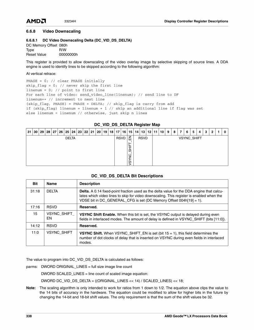
338 AMD Geode™ LX Processors Data Book
Display Controller Register Descriptions33234H
6.6.8 Video Downscaling
6.6.8.1 DC Video Downscaling Delta (DC_VID_DS_DELTA)
This register is provided to allow downscaling of the video overlay image by selective skipping of source lines. A DDAengine is used to identify lines to be skipped according to the following algorithm:
At vertical retrace:
PHASE = 0; // clear PHASE initially skip_flag = 0; // never skip the first line linenum = 0; // point to first line For each line of video: send_video_line(linenum); // send line to DF linenum++ // increment to next line{skip_flag, PHASE} = PHASE + DELTA; // skip_flag is carry from add if (skip_flag) linenum = linenum + 1 // skip an additional line if flag was setelse linenum = linenum // otherwise, just skip n lines
The value to program into DC_VID_DS_DELTA is calculated as follows:
parms: DWORD ORIGINAL_LINES = full size image line count
DWORD SCALED_LINES = line count of scaled image equation:
DWORD DC_VID_DS_DELTA = ((ORIGINAL_LINES << 14) / SCALED_LINES) << 18;
Note: The scaling algorithm is only intended to work for ratios from 1 down to 1/2. The equation above clips the value tothe 14 bits of accuracy in the hardware. The equation could be modified to allow for higher bits in the future bychanging the 14-bit and 18-bit shift values. The only requirement is that the sum of the shift values be 32.
DC Memory Offset 080hType R/WReset Value 00000000h
DC_VID_DS_DELTA Register Map
31 30 29 28 27 26 25 24 23 22 21 20 19 18 17 16 15 14 13 12 11 10 9 8 7 6 5 4 3 2 1 0
DELTA RSVD
VS
YN
C_S
HIF
T_E
N RSVD VSYNC_SHIFT
DC_VID_DS_DELTA Bit Descriptions
Bit Name Description
31:18 DELTA Delta. A 0.14 fixed-point fraction used as the delta value for the DDA engine that calcu-lates which video lines to skip for video downscaling. This register is enabled when the VDSE bit in DC_GENERAL_CFG is set (DC Memory Offset 004h[19] = 1).
17:16 RSVD Reserved.
15 VSYNC_SHIFT_EN
VSYNC Shift Enable. When this bit is set, the VSYNC output is delayed during even fields in interlaced modes. The amount of delay is defined in VSYNC_SHIFT (bits [11:0]).
14:12 RSVD Reserved.
11:0 VSYNC_SHIFT VSYNC Shift. When VSYNC_SHIFT_EN is set (bit 15 = 1), this field determines the number of dot clocks of delay that is inserted on VSYNC during even fields in interlaced modes.
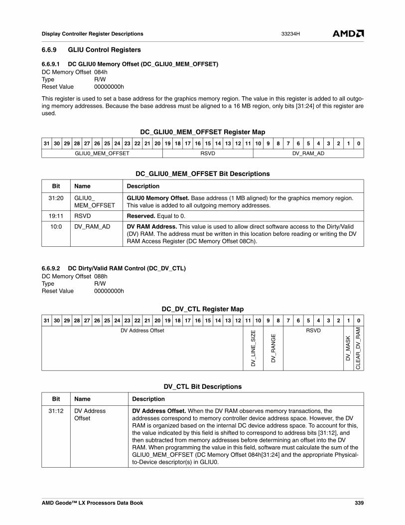
AMD Geode™ LX Processors Data Book 339
Display Controller Register Descriptions 33234H
6.6.9 GLIU Control Registers
6.6.9.1 DC GLIU0 Memory Offset (DC_GLIU0_MEM_OFFSET)
This register is used to set a base address for the graphics memory region. The value in this register is added to all outgo-ing memory addresses. Because the base address must be aligned to a 16 MB region, only bits [31:24] of this register areused.
6.6.9.2 DC Dirty/Valid RAM Control (DC_DV_CTL)
DC Memory Offset 084hType R/WReset Value 00000000h
DC_GLIU0_MEM_OFFSET Register Map
31 30 29 28 27 26 25 24 23 22 21 20 19 18 17 16 15 14 13 12 11 10 9 8 7 6 5 4 3 2 1 0
GLIU0_MEM_OFFSET RSVD DV_RAM_AD
DC_GLIU0_MEM_OFFSET Bit Descriptions
Bit Name Description
31:20 GLIU0_MEM_OFFSET
GLIU0 Memory Offset. Base address (1 MB aligned) for the graphics memory region. This value is added to all outgoing memory addresses.
19:11 RSVD Reserved. Equal to 0.
10:0 DV_RAM_AD DV RAM Address. This value is used to allow direct software access to the Dirty/Valid (DV) RAM. The address must be written in this location before reading or writing the DV RAM Access Register (DC Memory Offset 08Ch).
DC Memory Offset 088hType R/WReset Value 00000000h
DC_DV_CTL Register Map
31 30 29 28 27 26 25 24 23 22 21 20 19 18 17 16 15 14 13 12 11 10 9 8 7 6 5 4 3 2 1 0
DV Address Offset
DV
_LIN
E_S
IZE
DV
_RA
NG
E
RSVD
DV
_MA
SK
CLE
AR
_DV
_RA
M
DV_CTL Bit Descriptions
Bit Name Description
31:12 DV Address Offset
DV Address Offset. When the DV RAM observes memory transactions, the addresses correspond to memory controller device address space. However, the DV RAM is organized based on the internal DC device address space. To account for this, the value indicated by this field is shifted to correspond to address bits [31:12], and then subtracted from memory addresses before determining an offset into the DV RAM. When programming the value in this field, software must calculate the sum of the GLIU0_MEM_OFFSET (DC Memory Offset 084h[31:24] and the appropriate Physical-to-Device descriptor(s) in GLIU0.

340 AMD Geode™ LX Processors Data Book
Display Controller Register Descriptions33234H
6.6.9.3 DC Dirty/Valid RAM Access (DC_DV_ACCESS)
11:10 DV_LINE_SIZE DV Line Size. This field determines how many bytes of frame buffer space correspond to an entry in the DV RAM. The value selected by this field must be greater than or equal to the FB_LINE_SIZE, as programmed in the DC_LINE_SIZE register (DC Mem-ory Offset 030h[9:0]).
00: 1024 (256 QWORDs)01: 2048 (512 QWORDs)10: 4096 (1024 QWORDs)11: 8192 (2048 QWORDs)
9:8 DV_RANGE DV Range. The value selected by this field is an upper bound of the number of entries used in the DV RAM. By setting this value to a number less than the maximum (2048), there is a potential savings in power, since the DV RAM will not be accessed for lines that may be just above the frame buffer space.
00: 2048 lines01: 512 lines10: 1024 lines11: 1536 lines
7:2 RSVD Reserved. Set to 0.
1 DV_MASK DV MASK. While this bit is set, the DV RAM controller does not monitor writes to mem-ory; no DIRTY bits will be set in response to memory activity. When this bit is cleared, the DV RAM behaves normally.
0 CLEAR_DV_RAM Clear DV RAM. Writing a 1 to this bit causes the contents of the DV RAM to be cleared (i.e., every entry is set to dirty and invalid). This process requires approximately 2050 GLIU0 clocks. This bit may be read to determine if this clear operation is underway (1) or completed (0). Writing a 0 to this bit has no effect.
DC Memory Offset 08ChType R/WReset Value 0000000xh
DV_CTL Bit Descriptions (Continued)
Bit Name Description
DC_DV_ACCESS Register Map
31 30 29 28 27 26 25 24 23 22 21 20 19 18 17 16 15 14 13 12 11 10 9 8 7 6 5 4 3 2 1 0
RSVDD
V_V
ALI
D
DV
_DIR
TY
DC_DV_ACCESS Bit Descriptions
Bit Name Description
31:2 RSVD Reserved. Set to 0.
1 DV_VALID DV Valid. Writes to this register place the value of this bit into the “valid” entry of the DV RAM. Reads return the value of the “valid” entry. The DV RAM Address is determined by the value in DV_RAM_AD (DC Memory Offset 084h[10:0]).
0 DV_DIRTY DV Dirty. Writes to this register will place the value of this bit into the “dirty” entry of the dirty/valid RAM. Reads will return the value of the “dirty” entry. The DV RAM Address is determined by the value in DV_RAM_AD (DC Memory Offset 084h[10:0]).

AMD Geode™ LX Processors Data Book 341
Display Controller Register Descriptions 33234H
6.6.10 Graphics Scaling Control Registers
6.6.10.1 DC Graphics Filter Scale (DC_GFX_SCALE)DC Memory Offset 090hType R/WReset Value 40004000h
DC_GFX_SCALE Register Map
31 30 29 28 27 26 25 24 23 22 21 20 19 18 17 16 15 14 13 12 11 10 9 8 7 6 5 4 3 2 1 0
V_SCALE H_SCALE
DC_GFX_SCALE Bit Descriptions
Bit Name Description
31:16 V_SCALE Vertical Filter Scale. The value in this field, represents the number of vertical lines of source data that are consumed for every line of filtered data produced by the scaler filter. This field is treated as a rational number, with the decimal point between bits 30 and 29. To determine the value to be programmed into this field, use the following formula:
V_SCALE = (V_SOURCE / (V_DEST-1)) << 14
Where V_SOURCE is the height (in scan lines) of the frame buffer and V_DEST is the height (in scan lines) of the destination field.
The default value of this field (4000h) represents 1:1 scaling. This value must be pro-grammed when the vertical filter is disabled.
The value in this field must not exceed 8000h, which represents a 2:1 downscale ratio. If the width of the source image is more than 1024 pixels, scaling is not supported.
15:0 H_SCALE Horizontal Filter Scale. The value in this field, represents the number of (horizontal) pix-els of source data that are consumed for every pixel of data produced by the scaler filter. This field is treated as a rational number, with the decimal point between bits 14 and 13. To determine the value to be programmed into this field, use the following formula:
H_SCALE = (H_SOURCE/(H_DEST-1)) << 14
Where H_SOURCE is the width (in pixels) of the frame buffer and H_DEST is the width (in pixels) of the destination image.
The default value of this field (4000h) represents 1:1 scaling. This value must be pro-grammed when the horizontal filter is disabled.
The value in this field must never exceed 8000h, which represents a 2:1 horizontal down-scale. If the width of the source image is greater than 1024 pixels, scaling is not sup-ported.

342 AMD Geode™ LX Processors Data Book
Display Controller Register Descriptions33234H
6.6.10.2 DC IRQ/Filter Control (DC_IRQ_FILT_CTL)DC Memory Offset 094hType R/WReset Value 00000000h
DC_IRQ_FILT_CTL Register Map
31 30 29 28 27 26 25 24 23 22 21 20 19 18 17 16 15 14 13 12 11 10 9 8 7 6 5 4 3 2 1 0
RS
VD
LIN
EB
UF
_SE
L
INT
ER
LAC
E_A
DD
RE
SS
ING
RS
VD
LINE_COUNT
RS
VD
ALP
HA
_FIL
T_E
NA
RS
VD
FIL
T_E
NA
INT
L_E
N
H_F
ILT
_SE
L
RSVD FILT_ADDR
DC_IRQ_FILT_CTL Bit Descriptions
Bit Name Description
31 RSVD Reserved.
30:29 LINEBUF_SEL Line Buffer Select. When LINEBUF_REG_EN[0] is set (bit 9 = 1), the coefficient RAM address bits (FILT_ADDR, bits [7:0) and the Filter Coefficient Data registers (DC Memory Offset 098h and 09Ch) can be used to read and write the line buffer or flicker filter RAMs. This field selects which of the three line buffer RAMS (or two flicker filter RAMs) is to be accessed.
28 INTERLACE_ADDRESSING
Interlace Addressing. This bit indicates whether each field should be vertically deci-mated when interlacing. If this bit is set, each field of the interlaced frame will include every other line of the original (unscaled) frame buffer image. The flicker filter and scaler filter should both be disabled if this bit is set.
27 RSVD Reserved.
26:16 LINE_COUNT Interrupt Line Count. This value determines which scan line will trigger a line count interrupt. When the DC’s display engine reaches the line number determined by this value, it will assert an interrupt if IRQ_MASK is cleared (DC Memory Offset 0C8h[0] = 0).
15 RSVD Reserved.
14 ALPHA_FILT_ENA
Alpha Filter Enable. Settings written to this field will not take effect until the start of the following frame or interlaced field.
Setting this bit to 1 enables the scaler filter for the alpha channel. This filter is provided to support scaling and interlacing of graphics data. If the graphics filter is disabled or this bit is cleared, the alpha channel is not filtered; a nearest-neighbor mechanism is used instead. This can provide cleaner transitions between regions with significantly different alpha values.
13 RSVD Reserved.
12 FILT_ENA Graphics Filter Enable. Settings written to this field will not take effect until the start of the following frame or interlaced field.
Setting this bit to 1 enables the graphics scaler filter; This filter is provided to support scaling and interlacing of graphics data.

AMD Geode™ LX Processors Data Book 343
Display Controller Register Descriptions 33234H
6.6.10.3 DC Filter Coefficient Data Register 1 (DC_FILT_COEFF1)
Any read or write of this register causes a read or write of the horizontal or filter coefficient RAM. If this occurs while the dis-play is active, improper filtering of an output pixel can occur, which may cause temporary visual artifacts (speckling). Toavoid this, either disable the display or avoid accessing this register unless during vertical blank.
11 INTL_EN Interlace Enable. Settings written to this field will not take effect until the start of the fol-lowing frame or interlaced field.
Setting this bit to 1 configures the output to interlaced mode. In this mode, the vertical timings are based on the even timing registers for every other field. This bit must be set if the flicker filter or address interlacing is enabled.
When using the VGA and interlacing, the scaler must also be used (i.e., bit 12 of this reg-ister must be set).
10 H_FILT_SEL Horizontal Filter Select. Setting this bit to 1 allows access to the horizontal filter coeffi-cients via this register and the Filter Data Registers (DC Memory Offset 098h and 09Ch). When this bit is cleared, the vertical filter coefficients are accessed instead.
9:8 RSVD Reserved.
7:0 FILT_ADDR Filter Coefficient Address. This indicates which filter location is accessed through reads and writes of the DC Filter Coefficient Data Register 1 (DC Memory Offset 098h).
DC Memory Offset 098hType R/WReset Value xxxxxxxxh
DC_IRQ_FILT_CTL Bit Descriptions (Continued)
Bit Name Description
DC_FILT_COEFF1 Register Map
31 30 29 28 27 26 25 24 23 22 21 20 19 18 17 16 15 14 13 12 11 10 9 8 7 6 5 4 3 2 1 0
RSVD TAP3 TAP2 TAP1
DC_ FILT_COEFF1 Bit Descriptions
Bit Name Description
31:30 RSVD Reserved. Set to 0.
29:20 TAP3 Tap 3 Coefficient. This coefficient is used for the third tap in the filter (the lower tap of the vertical filter or the center tap of the horizontal filter). Each of the four components of the pixel color (Red, Green, Blue, and Alpha, if available) is expanded to 8 bits and then multiplied by this value before being summed with the weighted results of the other filter taps.
19:10 TAP2 Tap 2 Coefficient. This coefficient is used for the second tap in the filter (the center tap of the vertical filter or the second tap from the left in the horizontal filter).
9:0 TAP1 Tap 1 Coefficient. This coefficient is used for the first tap in the filter (the upper tap of the vertical filter or the leftmost tap of the horizontal filter).
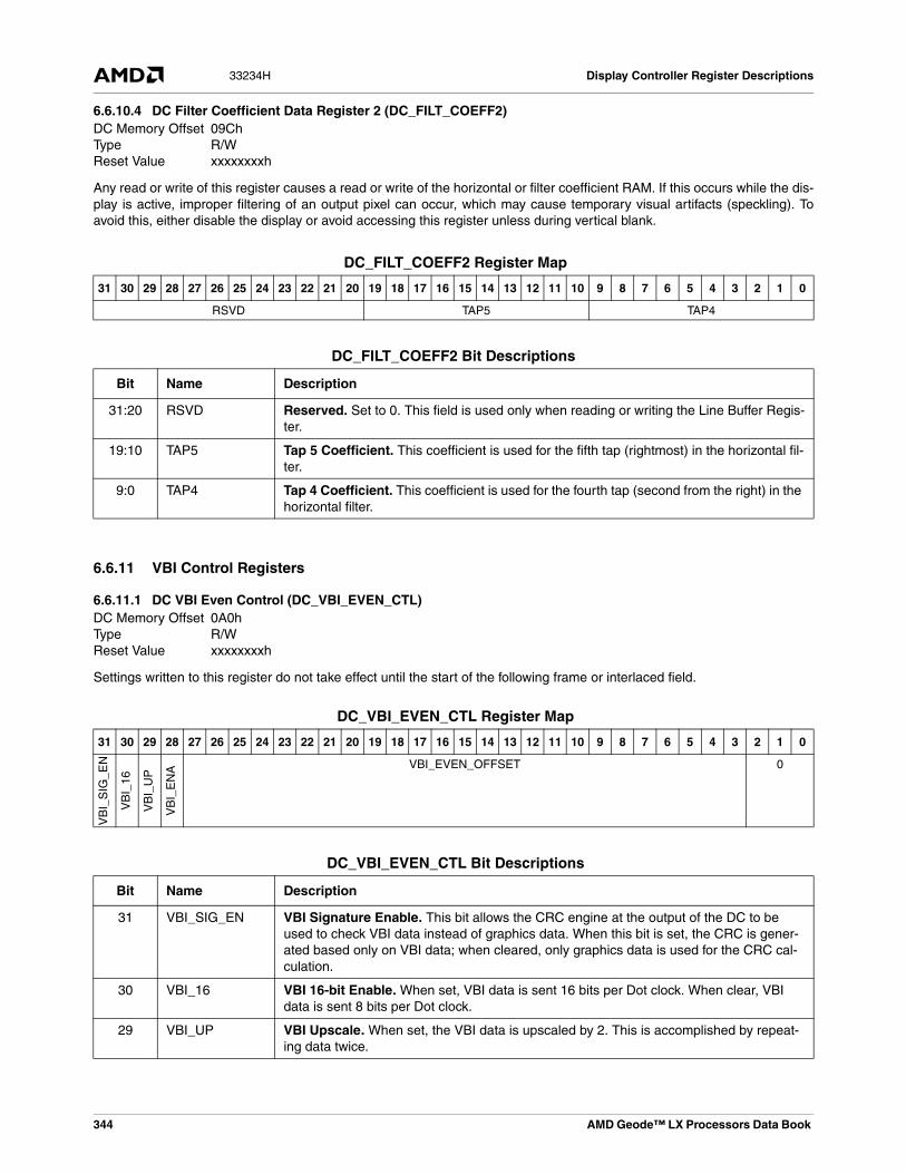
344 AMD Geode™ LX Processors Data Book
Display Controller Register Descriptions33234H
6.6.10.4 DC Filter Coefficient Data Register 2 (DC_FILT_COEFF2)
Any read or write of this register causes a read or write of the horizontal or filter coefficient RAM. If this occurs while the dis-play is active, improper filtering of an output pixel can occur, which may cause temporary visual artifacts (speckling). Toavoid this, either disable the display or avoid accessing this register unless during vertical blank.
6.6.11 VBI Control Registers
6.6.11.1 DC VBI Even Control (DC_VBI_EVEN_CTL)
Settings written to this register do not take effect until the start of the following frame or interlaced field.
DC Memory Offset 09ChType R/WReset Value xxxxxxxxh
DC_FILT_COEFF2 Register Map
31 30 29 28 27 26 25 24 23 22 21 20 19 18 17 16 15 14 13 12 11 10 9 8 7 6 5 4 3 2 1 0
RSVD TAP5 TAP4
DC_FILT_COEFF2 Bit Descriptions
Bit Name Description
31:20 RSVD Reserved. Set to 0. This field is used only when reading or writing the Line Buffer Regis-ter.
19:10 TAP5 Tap 5 Coefficient. This coefficient is used for the fifth tap (rightmost) in the horizontal fil-ter.
9:0 TAP4 Tap 4 Coefficient. This coefficient is used for the fourth tap (second from the right) in the horizontal filter.
DC Memory Offset 0A0hType R/WReset Value xxxxxxxxh
DC_VBI_EVEN_CTL Register Map
31 30 29 28 27 26 25 24 23 22 21 20 19 18 17 16 15 14 13 12 11 10 9 8 7 6 5 4 3 2 1 0
VB
I_S
IG_E
N
VB
I_16
VB
I_U
P
VB
I_E
NA VBI_EVEN_OFFSET 0
DC_VBI_EVEN_CTL Bit Descriptions
Bit Name Description
31 VBI_SIG_EN VBI Signature Enable. This bit allows the CRC engine at the output of the DC to be used to check VBI data instead of graphics data. When this bit is set, the CRC is gener-ated based only on VBI data; when cleared, only graphics data is used for the CRC cal-culation.
30 VBI_16 VBI 16-bit Enable. When set, VBI data is sent 16 bits per Dot clock. When clear, VBI data is sent 8 bits per Dot clock.
29 VBI_UP VBI Upscale. When set, the VBI data is upscaled by 2. This is accomplished by repeat-ing data twice.

AMD Geode™ LX Processors Data Book 345
Display Controller Register Descriptions 33234H
6.6.11.2 DC VBI Odd Control (DC_VBI_ODD_CTL)
Settings written to this register do not take effect until the start of the following frame or interlaced field.
6.6.11.3 DC VBI Horizontal Control (DC_VBI_HOR)
Settings written to this register do not take effect until the start of the following frame or interlaced field.
28 VBI_ENA VBI Enable. Setting this bit to 1 enables VBI (Vertical Blank Interrupt) data. This is a data stream that is placed in the off-screen region at the start of each field. This data is passed through the graphics output path, but is not filtered or modified in any way.
27:0 VBI_EVEN_OFFSET
VBI Even Address Offset. Indicates the starting offset for VBI data for even fields. This address must be QWORD aligned; the low three bits are always 0. If interlacing is dis-abled, this offset is used for VBI data.
DC Memory Offset 0A4hType R/WReset Value xxxxxxxxh
DC_VBI_EVEN_CTL Bit Descriptions (Continued)
Bit Name Description
DC_VBI_ODD_CTL Register Map
31 30 29 28 27 26 25 24 23 22 21 20 19 18 17 16 15 14 13 12 11 10 9 8 7 6 5 4 3 2 1 0
RSVD VBI_ODD_OFFSET 0
DC_VBI_ODD_CTL Bit Descriptions
Bit Name Description
31:28 RSVD Reserved. Set to 0.
27:0 VBI_ODD_OFFSET
VBI Odd Address Offset. Indicates the starting offset for VBI data for odd fields. This address must be QWORD aligned; the low three bits are always 0. If interlacing is dis-abled, the even offset is used for VBI data.
DC Memory Offset 0A8hType R/WReset Value xxxxxxxxh
DC_VBI_HOR Register Map
31 30 29 28 27 26 25 24 23 22 21 20 19 18 17 16 15 14 13 12 11 10 9 8 7 6 5 4 3 2 1 0
RSVD VBI_H_END RSVD VBI_H_START
DC_VBI_HOR Bit Descriptions
Bit Name Description
31:28 RSVD Reserved. Set to 0.
27:16 VBI_H_END VBI Horizontal End. Specifies the horizontal end position for VBI data minus 1 pixel.
15:12 RSVD Reserved. Set to 0.
11:0 VBI_H_START VBI Horizontal Start. Specifies the horizontal start position for VBI data minus 1 pixel.

346 AMD Geode™ LX Processors Data Book
Display Controller Register Descriptions33234H
6.6.11.4 DC VBI Odd Line Enable (DC_VBI_LN_ODD)
Settings written to this register do not take effect until the start of the following frame or interlaced field.
6.6.11.5 DC VBI Even Line Enable (DC_VBI_LN_EVEN)
Settings written to this register do not take effect until the start of the following frame or interlaced field.
DC Memory Offset 0AChType R/WReset Value xxxxxxxxh
DC_VBI_LN_ODD Register Map
31 30 29 28 27 26 25 24 23 22 21 20 19 18 17 16 15 14 13 12 11 10 9 8 7 6 5 4 3 2 1 0
LN_OFFSET_ODD LN_EN_ODD RSVD
DC_VBI_LN_ODD Bit Descriptions
Bit Name Description
31:25 LN_OFFSET_ODD
Odd Line Offset. Specifies the offset (in lines) of the start of VBI data from the initial edge of VSYNC. This field is not used if interlacing is disabled. This field must be set to a value of 126 or less.
24:2 LN_EN_ODD Odd Line Enable. Each of the bits in this field corresponds to a line (24-2) of VBI data. Setting a bit in this field to 1 enables the corresponding line of VBI data in the odd field. This field is not used if interlacing is disabled.
1:0 RSVD Reserved. Set to 0.
DC Memory Offset 0B0hType R/WReset Value xxxxxxxxh
DC_VBI_LN_EVEN Register Map
31 30 29 28 27 26 25 24 23 22 21 20 19 18 17 16 15 14 13 12 11 10 9 8 7 6 5 4 3 2 1 0
LN_OFFSET_EVEN LN_EN_EVEN RSVD
DC_VBI_LN_EVEN Bit Descriptions
Bit Name Description
31:25 LN_OFFSET_EVEN
Even Line Offset. Specifies the offset (in lines) of the start of VBI data from the initial edge of VSYNC. This field is used for all frames if interlacing is disabled. This field must be set to a value of 126 or less.
24:2 LN_EN_EVEN Even Line Enable. Each of the bits in this field corresponds to a line (24-2) of VBI data. Setting a bit in this field to 1 enables the corresponding line of VBI data in the even field. This field is used for all frames if interlacing is disabled.
1:0 RSVD Reserved. Set to 0.

AMD Geode™ LX Processors Data Book 347
Display Controller Register Descriptions 33234H
6.6.11.6 DC VBI Pitch and Size (DC_VBI_PITCH)
6.6.12 Color Key Control Registers
6.6.12.1 DC Color Key (DC_CLR_KEY)
DC Memory Offset 0B4hType R/WReset Value xxxxxxxxh
DC_VBI_PITCH Register Map
31 30 29 28 27 26 25 24 23 22 21 20 19 18 17 16 15 14 13 12 11 10 9 8 7 6 5 4 3 2 1 0
RSVD VBI_Size VBI_Pitch
DC_VBI_PITCH Bit Descriptions
Bit Name Description
31:26 RSVD Reserved. Set to 0.
25:16 VBI_SIZE VBI Data Size. Indicates how many QWORDs of data to fetch from memory for each line of VBI
15:0 VBI_PITCH VBI Data Pitch. Indicates how many QWORDs of memory space to increment when moving from the start of one active VBI line to the start of the next.
DC Memory Offset 0B8hType R/WReset Value 00000000h
DC_CLR_KEY Register Map
31 30 29 28 27 26 25 24 23 22 21 20 19 18 17 16 15 14 13 12 11 10 9 8 7 6 5 4 3 2 1 0
RSVD
CLR
_KE
Y_E
N CLR_KEY
DC_CLR_KEY Bit Descriptions
Bit Name Description
31:25 RSVD Reserved. Set to 0.
24 CLR_KEY_EN Color Key Enable. This bit enables color key detection in the DC. When this bit is set, the DC adjusts the alpha value of pixels whose 24-bit RGB values match the value in CLR_KEY (bits [23:0]). A mask is also provided in CLR_KEY_MASK (DC Memory Offset 0BCh[23:0]) to indicate which bits can be ignored when performing this match. Color key detection is performed after the data has been decompressed and the cursor has been overlayed, but before scaling and filtering take place.
23:0 CLR_KEY Color Key. This field represents the RGB value that will be compared to DC pixels when performing color key detection.

348 AMD Geode™ LX Processors Data Book
Display Controller Register Descriptions33234H
6.6.12.2 DC Color Key Mask (DC_CLR_KEY_MASK)
6.6.12.3 DC Color Key Horizontal Position (DC_CLR_KEY_X)
Settings written to this register do not take effect until the start of the following frame or interlaced field.
6.6.12.4 DC Color Key Vertical Position (DC_CLR_KEY_Y)
Settings written to this register do not take effect until the start of the following frame or interlaced field.
DC Memory Offset 0BChType R/WReset Value 00xxxxxxh
DC_CLR_KEY_MASK Register Map
31 30 29 28 27 26 25 24 23 22 21 20 19 18 17 16 15 14 13 12 11 10 9 8 7 6 5 4 3 2 1 0
RSVD CLR_KEY_MASK
DC_CLR_KEY_MASK Bit Descriptions
Bit Name Description
31:24 RSVD Reserved. Set to 0.
23:0 CLR_KEY_MASK
Color Key Mask. This field is ANDed with both the pixel and the color key value (in DC_CLR_KEY, DC Memory Offset 0B8h[23:0]) before comparing the values. This allows the value of some bits to be ignored when performing the match.
DC Memory Offset 0C0hType R/WReset Value 00000000h
DC_CLR_KEY_X Register Map
31 30 29 28 27 26 25 24 23 22 21 20 19 18 17 16 15 14 13 12 11 10 9 8 7 6 5 4 3 2 1 0
RSVD CLR_KEY_X_END RSVD CLR_KEY_X_START
DC_CLR_KEY_X Bit Descriptions
Bit Name Description
31:27 RSVD Reserved. Set to 0.
26:16 CLR_KEY_X_END
Color Key Horizontal End. This field indicates the horizontal end position of the color key region minus 1.This represents the first pixel past the end of the color key region. This field is 0-based; the upper left pixel of the screen is represented by (0,0).
15:11 RSVD Reserved. Set to 0.
10:0 CLR_KEY_X_START
Color Key Horizontal Start. This field represents the horizontal start position of the color key region minus 1. This represents the first pixel within the color key region.
DC Memory Offset 0C4hType R/WReset Value 00000000h
DC_CLR_KEY_Y Register Map
31 30 29 28 27 26 25 24 23 22 21 20 19 18 17 16 15 14 13 12 11 10 9 8 7 6 5 4 3 2 1 0
RSVD CLR_KEY_Y_END RSVD CLR_KEY_Y_START
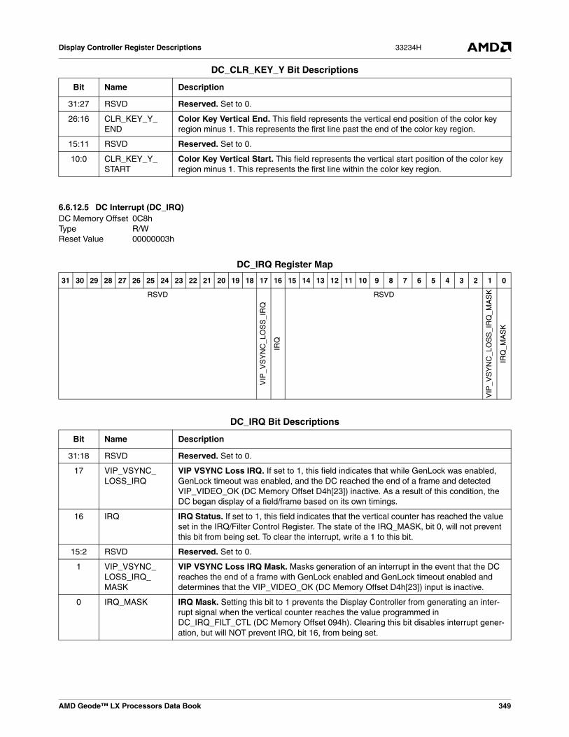
AMD Geode™ LX Processors Data Book 349
Display Controller Register Descriptions 33234H
6.6.12.5 DC Interrupt (DC_IRQ)
DC_CLR_KEY_Y Bit Descriptions
Bit Name Description
31:27 RSVD Reserved. Set to 0.
26:16 CLR_KEY_Y_END
Color Key Vertical End. This field represents the vertical end position of the color key region minus 1. This represents the first line past the end of the color key region.
15:11 RSVD Reserved. Set to 0.
10:0 CLR_KEY_Y_START
Color Key Vertical Start. This field represents the vertical start position of the color key region minus 1. This represents the first line within the color key region.
DC Memory Offset 0C8hType R/WReset Value 00000003h
DC_IRQ Register Map
31 30 29 28 27 26 25 24 23 22 21 20 19 18 17 16 15 14 13 12 11 10 9 8 7 6 5 4 3 2 1 0
RSVD
VIP
_VS
YN
C_L
OS
S_I
RQ
IRQ
RSVD
VIP
_VS
YN
C_L
OS
S_I
RQ
_MA
SK
IRQ
_MA
SK
DC_IRQ Bit Descriptions
Bit Name Description
31:18 RSVD Reserved. Set to 0.
17 VIP_VSYNC_LOSS_IRQ
VIP VSYNC Loss IRQ. If set to 1, this field indicates that while GenLock was enabled, GenLock timeout was enabled, and the DC reached the end of a frame and detected VIP_VIDEO_OK (DC Memory Offset D4h[23]) inactive. As a result of this condition, the DC began display of a field/frame based on its own timings.
16 IRQ IRQ Status. If set to 1, this field indicates that the vertical counter has reached the value set in the IRQ/Filter Control Register. The state of the IRQ_MASK, bit 0, will not prevent this bit from being set. To clear the interrupt, write a 1 to this bit.
15:2 RSVD Reserved. Set to 0.
1 VIP_VSYNC_LOSS_IRQ_MASK
VIP VSYNC Loss IRQ Mask. Masks generation of an interrupt in the event that the DC reaches the end of a frame with GenLock enabled and GenLock timeout enabled and determines that the VIP_VIDEO_OK (DC Memory Offset D4h[23]) input is inactive.
0 IRQ_MASK IRQ Mask. Setting this bit to 1 prevents the Display Controller from generating an inter-rupt signal when the vertical counter reaches the value programmed in DC_IRQ_FILT_CTL (DC Memory Offset 094h). Clearing this bit disables interrupt gener-ation, but will NOT prevent IRQ, bit 16, from being set.

350 AMD Geode™ LX Processors Data Book
Display Controller Register Descriptions33234H
6.6.13 Interrupt and GenLock Registers
6.6.13.1 DC GenLock Control (DC_GENLK_CTL)
Settings written to this register do not take effect until the start of the frame or interlaced field after the timing registerupdate bit (DC Memory Offset 008h[6]) is set.
DC Memory Offset 0D4hType R/WReset Value xxxxxxxxh
DC_GENLK_CTL Register Map
31 30 29 28 27 26 25 24 23 22 21 20 19 18 17 16 15 14 13 12 11 10 9 8 7 6 5 4 3 2 1 0
FLICK_SEL RSVD
ALP
HA
_FLI
CK
_EN
FLI
CK
_EN
VIP
_VID
EO
_OK
GE
NLO
CK
_AC
TIV
E
SK
EW
_WA
IT
VIP
_VS
YN
C_W
AIT
GE
NLK
_TO
_EN
GE
NLK
_EN
GENLK_SKW
DC_GENLK_CTL Bit Descriptions
Bit Name Description
31:28 FLICK_SEL Flicker Filter Select. When the flicker filter is enabled (FLICK_EN, bit 24 = 1), this field selects the weighting of the three taps in this vertical filter:
0000: 0, 1, 0 (top, middle, bottom)
0001: 1/16, 7/8, 1/16
0010: 1/8, 3/4, 1/8
0100: 1/4, 1/2, 1/4
0101: 5/16, 3/8, 5/16
All other combinations in this field are reserved.
27:26 RSVD Reserved. Set to 0.
25 ALPHA_FLICK_EN
Alpha Flicker Filter Enable. If set, this bit enables flicker filtering of the alpha value when the flicker filter is enabled (FLICK_EN, bit 24 = 1). If the flicker filter is enabled and this bit is cleared, the alpha value of the center pixel is passed through the flicker filter unchanged.
24 FLICK_EN Flicker Filter Enable. Enables the 3-tap vertical flicker filter (primarily used for interlaced modes). When set, the graphics output is filtered vertically using the coefficients as indi-cated in bits [22:21]. When clear, no flicker filtering is performed.
23 VIP_VIDEO_OK (RO)
VIP Video OK (Read Only). This bit indicates the state of the internal VIP VIDEO_OK input. This signal is driven by the VIP to indicate that the VIP is detecting a valid input stream.
22 GENLOCK_ACTIVE (RO)
GenLock Active (Read Only). This bit indicates that the current (or most recent) field/frame was initiated as the result of an active VIP VSYNC. The state of this bit will change coincident with the activation of the VSYNC output. If the VSYNC output occurs as the result of a timeout condition, this bit will be cleared. If GenLock is not enabled (GENLK_EN, bit 18 = 0), this bit will be cleared.
21 SKEW_WAIT (RO)
Skew Wait (Read Only). This status bit indicates that the DC has received a VSYNC from the VIP and that the skew counter is running. This bit is set when the VIP_VSYNC input is set and cleared when the skew counter expires.

AMD Geode™ LX Processors Data Book 351
Display Controller Register Descriptions 33234H
6.6.14 Even Field Video Address Registers
6.6.14.1 DC Even Field Video Y Start Address Offset (DC_VID_EVEN_Y_ST_OFFSET)
Settings written to this register do not take effect until the start of the next even interlaced field.
20 VIP_VSYNC_WAIT (RO)
VIP VSYNC Wait (Read Only). If set to 1 this status bit indicates that the DC has com-pleted a field or frame and is waiting for the VIP’s VSYNC to go active before beginning another frame. Typically, this will occur only if the VIP_VIDEO_OK (bit 23) input is active or the GENLOCK_TO _EN (bit 19) is inactive.
19 GENLK_TO_EN GenLock Time Out Enable. Setting this bit allows the DC to revert to its own internal timer if a loss of sync is detected by the VIP. This allows for seamless operation of the DC in GenLock mode when the VIP input becomes unstable. Clearing this bit forces the DC to wait for a VSYNC signal from the VIP even if the VIP indicates a loss of sync.
18 GENLK_EN GenLock Enable. When set to 1, the DC resets to the start of the frame/field upon receipt of a rising edge on the VIP_VSYNC signal.
17:0 GENLK_SKW GenLock Skew. This value indicates how many Dot clocks to delay the internal recogni-tion of the VIP VSYNC by the DC when GenLock is enabled. If GenLock timeout is also enabled (GENLK_TO_EN, bit 19 = 1), internal recognition of VSYNC occurs immediately upon timeout (without allowing this skew time to elapse after the timeout is detected.) This allows seamless transition from a VIP-supplied VSYNC to an internally-determined VSYNC, while still allowing for a delay in timeout detection.
DC Memory Offset 0D8hType R/WReset Value xxxxxxxxh
DC_GENLK_CTL Bit Descriptions (Continued)
Bit Name Description
DC_VID_EVEN_Y_ST_OFFSET Register Map
31 30 29 28 27 26 25 24 23 22 21 20 19 18 17 16 15 14 13 12 11 10 9 8 7 6 5 4 3 2 1 0
RSVD OFFSET
DC_VID_EVEN_Y_ST_OFFSET Bit Descriptions
Bit Name Description
31:28 RSVD Reserved. Set to 0.
27:0 OFFSET Video Y Even Buffer Start Offset. This value represents the starting location for Video Y Buffer for even fields when interlacing is enabled. This field is not used when interlac-ing is disabled (DC Memory Offset 094h[11] = 0).
This value represents the starting location for Video Y Buffer for even fields when inter-lacing is enabled (DC Memory Offset 094h[11] = 1). The lower five bits should always be programmed as zero so that the start offset is aligned to a 32-byte boundary. If YUV 4:2:2 mode is selected (DC Memory Offset 004h[20] = 0), the Video Y Buffer is used as a singular buffer holding interleaved Y, U and V data. If YUV 4:2:0 is selected (DC Memory Offset 004h[20] = 1), the Video Y Buffer is used to hold only Y data while U and V data are stored in separate buffers.
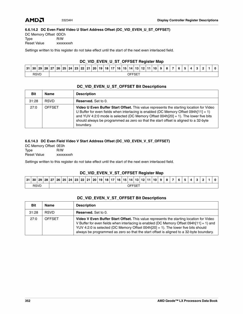
352 AMD Geode™ LX Processors Data Book
Display Controller Register Descriptions33234H
6.6.14.2 DC Even Field Video U Start Address Offset (DC_VID_EVEN_U_ST_OFFSET)
Settings written to this register do not take effect until the start of the next even interlaced field.
6.6.14.3 DC Even Field Video V Start Address Offset (DC_VID_EVEN_V_ST_OFFSET)
Settings written to this register do not take effect until the start of the next even interlaced field.
DC Memory Offset 0DChType R/WReset Value xxxxxxxxh
DC_VID_EVEN_U_ST_OFFSET Register Map
31 30 29 28 27 26 25 24 23 22 21 20 19 18 17 16 15 14 13 12 11 10 9 8 7 6 5 4 3 2 1 0
RSVD OFFSET
DC_VID_EVEN_U_ST_OFFSET Bit Descriptions
Bit Name Description
31:28 RSVD Reserved. Set to 0.
27:0 OFFSET Video U Even Buffer Start Offset. This value represents the starting location for Video U Buffer for even fields when interlacing is enabled (DC Memory Offset 094h[11] = 1) and YUV 4:2:0 mode is selected (DC Memory Offset 004h[20] = 1). The lower five bits should always be programmed as zero so that the start offset is aligned to a 32-byte boundary.
DC Memory Offset 0E0hType R/WReset Value xxxxxxxxh
DC_VID_EVEN_V_ST_OFFSET Register Map
31 30 29 28 27 26 25 24 23 22 21 20 19 18 17 16 15 14 13 12 11 10 9 8 7 6 5 4 3 2 1 0
RSVD OFFSET
DC_VID_EVEN_V_ST_OFFSET Bit Descriptions
Bit Name Description
31:28 RSVD Reserved. Set to 0.
27:0 OFFSET Video V Even Buffer Start Offset. This value represents the starting location for Video V Buffer for even fields when interlacing is enabled (DC Memory Offset 094h[11] = 1) and YUV 4:2:0 is selected (DC Memory Offset 004h[20] = 1). The lower five bits should always be programmed as zero so that the start offset is aligned to a 32-byte boundary.

AMD Geode™ LX Processors Data Book 353
Display Controller Register Descriptions 33234H
6.6.15 Even Field Vertical Timing Registers
6.6.15.1 DC Vertical and Total Timing for Even Fields (DC_V_ACTIVE_EVEN_TIMING)
This register contains vertical active and total timing information. These parameters pertain ONLY to even fields in inter-laced display modes (The DC_V_ACTIVE_TIMING register (DC Memory Offset 050h) will take effect for odd fields in inter-laced display modes.) Settings written to this register will not take effect until the start of the frame or interlaced field afterthe timing register update bit is set (DC Memory Offset 008h[6] = 1).
DC Memory Offset 0E4hType R/WReset Value xxxxxxxxh
DC_V_ACTIVE_EVEN_TIMING Register Map
31 30 29 28 27 26 25 24 23 22 21 20 19 18 17 16 15 14 13 12 11 10 9 8 7 6 5 4 3 2 1 0
RSVD V_TOTAL RSVD V_ACTIVE
DC_V_ACTIVE_EVEN_TIMING Bit Descriptions
Bit Name Description
31:27 RSVD Reserved. These bits should be programmed to zero.
26:16 V_TOTAL Vertical Total. This field represents the total number of lines for a given frame scan minus 1. Note that the value is necessarily greater than the V_ACTIVE field (bits 10:0]) because it includes border lines and blanked lines.
15:11 RSVD Reserved. These bits should be programmed to zero.
10:0 V_ACTIVE Vertical Active. This field represents the total number of lines for the displayed portion of a frame scan minus 1. Note that for flat panels, if this value is less than the panel active vertical resolution (V_PANEL), the parameters V_BLANK_START, V_BLANK_END, V_SYNC_START, and V_SYNC_END should be reduced by the following value (V_ADJUST) to achieve vertical centering:
V_ADJUST = (V_PANEL - V_ACTIVE) / 2
If graphics scaling is enabled (and interleaved display is enabled), this value represents the height of the final (scaled) field to be displayed. The height of the frame buffer image may be different in this case; FB_ACTIVE (DC Memory Offset 5Ch) is used to program the horizontal and vertical active values in the frame buffer when graphics scaling is enabled.

354 AMD Geode™ LX Processors Data Book
Display Controller Register Descriptions33234H
6.6.15.2 DC CRT Vertical Blank Timing for Even Fields (DC_V_BLANK_EVEN_TIMING)
This register contains vertical blank timing information. All values are specified in lines. This register is used ONLY for evenfields in interlaced display modes. Settings written to this register do not take effect until the start of the frame or interlacedfield after the timing register update bit is set (DC Memory Offset 008h[6] = 1).
6.6.15.3 DC CRT Vertical Sync Timing for Even Fields (DC_V_SYNC_EVEN_TIMING)
This register contains CRT vertical sync timing information. All values are specified in lines. This register is used ONLY foreven fields in interlaced modes. Settings written to this register do not take effect until the start of the frame or interlacedfield after the timing register update bit is set (DC Memory Offset 008h[6] = 1).
DC Memory Offset 0E8hType R/WReset Value xxxxxxxxh
DC_V_BLANK_EVEN_TIMING Register Map
31 30 29 28 27 26 25 24 23 22 21 20 19 18 17 16 15 14 13 12 11 10 9 8 7 6 5 4 3 2 1 0
RSVD V_BLANK_END RSVD V_BLANK_START
DC_V_BLANK_EVEN_TIMING Bit Descriptions
Bit Name Description
31:27 RSVD Reserved. These bits should be programmed to zero.
26:16 V_BLANK_END Vertical Blank End. This field represents the line at which the vertical blanking signal becomes inactive minus 1. If the display is interlaced, no border is supported, so this value should be identical to V_TOTAL (DC Memory Offset 0E4h[26:16]).
15:11 RSVD Reserved. These bits should be programmed to zero.
10:0 V_BLANK_START
Vertical Blank Start. This field represents the line at which the vertical blanking signal becomes active minus 1. If the display is interlaced, this value should be programmed to V_ACTIVE (DC Memory Offset 0E4h[10:0]) plus 1.
DC Memory Offset 0EChType R/WReset Value xxxxxxxxh
DC_V_SYNC_EVEN_TIMING Register Map
31 30 29 28 27 26 25 24 23 22 21 20 19 18 17 16 15 14 13 12 11 10 9 8 7 6 5 4 3 2 1 0
RSVD V_SYNC_END RSVD V_SYNC_START
DC_V_SYNC_EVEN_TIMING Bit Descriptions
Bit Name Description
31:27 RSVD Reserved. These bits should be programmed to zero.
26:16 V_SYNC_END Vertical Sync End. This field represents the line at which the CRT vertical sync signal becomes inactive minus 1.
15:11 RSVD Reserved. These bits should be programmed to zero.
10:0 V_SYNC_START
Vertical Sync Start. This field represents the line at which the CRT vertical sync signal becomes active minus 1. For interlaced display, note that the vertical counter is incre-mented twice during each line and since there are an odd number of lines, the vertical sync pulse will trigger in the middle of a line for one field and at the end of a line for the subsequent field.

AMD Geode™ LX Processors Data Book 355
Display Controller Register Descriptions 33234H
6.6.16 VGA Block Configuration Registers
6.6.16.1 VGA Configuration (VGA_CONFIG)
This register controls palette write operations.
6.6.16.2 VGA Status (VGA_STATUS)
This register provides status information for the individual SMI events enabled in the VGA_CONFIG register (DC MemoryOffset 100h), as well as certain other status bits. Reading this register clears all active events.
DC Memory Offset 100hType R/WReset Value 00000000h
VGA_CONFIG Register Map
31 30 29 28 27 26 25 24 23 22 21 20 19 18 17 16 15 14 13 12 11 10 9 8 7 6 5 4 3 2 1 0
RSVD
WP
PAL
VGA_CONFIG Bit Descriptions
Bit Name Description
31:1 RSVD Reserved. Set to 0.
0 WPPAL Write Protect Palette. If set to 1, VGA palette write operations are NOT written to the palette RAMs. Palette writes behave normally, except that the data is discarded.
DC Memory Offset 104hType ROReset Value 00000000h
VGA_STATUS Register Map
31 30 29 28 27 26 25 24 23 22 21 20 19 18 17 16 15 14 13 12 11 10 9 8 7 6 5 4 3 2 1 0
RSVD BLINK_CNT RSVD V_CNT RSVD
VS
YN
C
DIS
PE
N
CR
TC
IO_S
MI
VB
LAN
K_S
MI
ISR
0_S
MI
MIS
C_S
MI
VGA_STATUS Bit Descriptions
Bit Name Description
31:30 RSVD Reserved.
29:24 BLINK_CNT Blink Counter Value. Unsynchronized, used as a simulation aid.
23:22 RSVD Reserved.
21:12 V_CNT Vertical Counter Value. Unsynchronized, used as a simulation aid.
11:6 RSVD Reserved.
5 VSYNC VSYNC. 1 If VSYNC is active (copy of bit 3 of ISR1).
4 DISPEN Display Enable. 0 if both horizontal and vertical display enable are active (copy of bit 0 of ISR1).
3 CRTCIO_SMI CRTC Register SMI. If = 1, an SMI was generated due to an I/O read or write to an non-implemented CRTC register.

356 AMD Geode™ LX Processors Data Book
Display Controller Register Descriptions33234H
6.6.17 VGA Block Standard Registers
6.6.17.1 VGA Miscellaneous Output
2 VBLANK_SMI VBLANK SMI. If = 1, an SMI was generated due to leading edge vertical blank.
1 ISR0_SMI Input Status Register 0 SMI. If = 1, an SMI was generated from an I/O IN to Input Status Register 0.
0 MISC_SMI Miscellaneous Output Register SMI. If = 1, an SMI was generated from an I/O OUT to the Miscellaneous Output Register.
Read Address 3CChWrite Address 3C2hType R/WReset Value 02h
VGA_STATUS Bit Descriptions (Continued)
Bit Name Description
VGA Miscellaneous Output Register Bit Descriptions
Bit Name Description
7 VSYNC_POL Vertical Sync Polarity. Selects a positive-going VSYNC pulse (bit = 0) or a negative-going VSYNC pulse (bit = 1).
6 HSYNC_POL Horizontal Sync Polarity. Selects a positive-going HSYNC pulse (bit = 0) or a negative-going HSYNC pulse (bit = 1).
5 PAGE Page Bit. This bit is used to replace memory address bit A0 as the LSB when bit 1 of the Miscellaneous register (Index 06h[1]) in the VGA Graphics Controller is set to 1.
4 RSVD Reserved.
3:2 CLK_SEL Clock Select. Selects the VGA pixel clock source. Writes to this register will directly affect the frequency generated by the Dot clock PLLs. The value of this register is sam-pled when it is written; The Dot clock frequency can be overridden by subsequent writes to the Dot clock PLL controls. If the VGA is disabled or in fixed timing mode, the Dot clock frequency is NOT affected by writes to this register.
00: Selects clock for 640/320 pixels per line (25.175 MHz Dot clock).01: Selects clock for 720/360 pixels per line (28.325 MHz Dot clock).10: Reserved.11: Reserved.
1 RAM_EN RAM Enable. Enables the video frame buffer address decode when set to 1.
0 ID_ADDR_SEL I/O Address Select. Determines the I/O address of the CRTC Index and Data registers (Index 3?4h and 3?5h), Feature Control register (Index 3?Ah), and Input Status Register 1 (Index 3?Ah) as follows: ? = B when bit set to 0 (MDA I/O address emulation), ? = D when bit set to 1 (CGA address emulation).

AMD Geode™ LX Processors Data Book 357
Display Controller Register Descriptions 33234H
6.6.17.2 VGA Input Status Register 0
6.6.17.3 VGA Input Status Register 1
6.6.17.4 VGA Feature Control
Read Address 3C2hWrite Address --Type R/WReset Value 00h
VGA Input Status Register 0 Bit Descriptions
Bit Name Description
7 RSVD Not Implemented. (CRTC Interrupt Pending)
6:5 RSVD Reserved.
4 RSVD Not Implemented. (Display Sense)
3:0 RSVD Reserved.
Read Address 3BAh or 3DAhWrite Address --Type R/WReset Value 01h
VGA Input Status Register 1 Bit Descriptions
Bit Name Description
7:4 RSVD Reserved.
3 VSYNC Vertical SYNC. When a 1, indicates that the VSYNC signal is active.
2:1 RSVD Reserved.
0 DISP_EN Display Enable. Reads as a 0 when both horizontal and vertical display enable are active. Reads as a 1 when either display enable signal is inactive.
Read Address 3CAhWrite Address 3BAh or 3DAhType R/WReset Value xxh
VGA Feature Control Register Bit Descriptions
Bit Name Description
7:0 RSVD Reserved.

358 AMD Geode™ LX Processors Data Book
Display Controller Register Descriptions33234H
6.6.18 VGA Sequencer RegistersThe Sequencer registers are accessed by writing an index value to the Sequencer Index register (3C4h) and reading orwriting the register using the Sequencer Data register (3C5h).
6.6.18.1 VGA Sequencer Index
6.6.18.2 VGA Sequencer Data
6.6.18.3 VGA Reset
Table 6-51. VGA Sequencer Registers Summary
Index Type Register Reset Value Reference
-- R/W VGA Sequencer Index 0xh Page 358
-- R/W VGA Sequencer Data xxh Page 358
00h R/W VGA Reset 00h Page 358
01h R/W VGA Clocking Mode 02h Page 359
02h R/W VGA Map Mask 00h Page 359
03h R/W VGA Character Map Select xxh Page 360
04h R/W VGA Memory Mode 02h Page 360
Index Address 3C4hType R/WReset Value 0xh
VGA Sequencer Index Register Bit Descriptions
Bit Name Description
7:3 RSVD Reserved.
2:0 INDEX Index.
Data Address 3C5hType R/WReset Value xxh
VGA Sequencer Data Register Bit Descriptions
Bit Name Description
7:0 DATA Data.
Index 00hType R/WReset Value 00h
VGA Reset Register Bit Descriptions
Bit Name Description
7:2 RSVD Reserved.
1:0 DIS_EN Enable Display. Both these bits should be set to 1 (value = 11) to enable display of the VGA screen image. If either of these bits are 0, the display is blanked. The VGA contin-ues to respond to I/O and memory accesses.

AMD Geode™ LX Processors Data Book 359
Display Controller Register Descriptions 33234H
6.6.18.4 VGA Clocking Mode
6.6.18.5 VGA Map Mask
These bits enable (bit = 1) writing to their corresponding bytes in each DWORD of the frame buffer (i.e., EM3 enables byte3, EM2 enables byte 2, etc.). The four maps or planes correspond to the four bytes in each DWORD of the frame buffer.Reads to all maps are always enabled, and are unaffected by these bits.
Index 01hType R/WReset Value 02h
VGA Clocking Mode Register Bit Descriptions
Bit Name Description
7:6 RSVD Reserved.
5 SCREEN_OFF Screen Off. Setting this bit to a 1 blanks the screen while maintaining the HSYNC and VSYNC signals. This is intended to allow the CPU full access to the memory bandwidth. This bit must be 0 for the display image to be visible.
4 RSVD Not Supported. (Shift4)
3 DCLK_DIV2 Dot Clock Divide By 2. When set to 1, the incoming pixel clock is divided by two to form the actual Dot clock. When 0, the incoming pixel clock is used unchanged.
2 RSVD Not Supported. (Shift Load)
1 RSVD Reserved. Always 1.
0 CHAR_WIDTH 8-Dot Character Width. When set to a 1, the character cells in text mode are eight pixels wide. When set to 0, the character cells are nine pixels wide. The 9th pixel is equal to the 8th pixel for character codes C0h-DFh (the line graphics character codes), and is 0 (background) for all other codes.
Index 02hType R/WReset Value 00h
VGA Map Mask Register Bit Descriptions
Bit Name Description
7:4 RSVD Reserved.
3 EM3 Enable Map 3.
2 EM2 Enable Map 2.
1 EM1 Enable Map 1.
0 EM0 Enable Map 0.

360 AMD Geode™ LX Processors Data Book
Display Controller Register Descriptions33234H
6.6.18.6 VGA Character Map Select
Character Map A (bits [5,3:2]) and Character Map B (bits [4,1:0]) determine which font tables are used when displaying acharacter in text mode. When bit 3 of the character's attribute = 1, Character Map A is used; when bit 3 of the character'sattribute = 0, Character Map B is used. The font tables are stored in the 64 KB in map 2. There are eight font tables. Thecharacter map codes select the font tables as shown in Table 6-52.
6.6.18.7 VGA Memory Mode
Index 03hType R/WReset Value xxh
VGA Character Map Select Register Bit Descriptions
Bit Name Description
7:6 RSVD Reserved. Write as read.
5 CHAR_AZ Character Map A bit 2.
4 CHAR_BZ Character Map B bit 2.
3:2 CHAR_A Character Map A bits 1:0.
1:0 CHAR_B Character Map B bits 1:0.
Table 6-52. Font Table
Code Font Table Location in Map 2 Code Font Table Location in Map 2
0 8 KB Block 0 4 8 KB Block 1
1 8 KB Block 2 5 8 KB Block 3
2 8 KB Block 4 6 8 KB Block 5
3 8 KB Block 6 7 8 KB Block 7
Index 04hType R/WReset Value 02h
VGA Memory Mode Register Bit Descriptions
Bit Name Description
7:4 RSVD Reserved.
3 CHAIN4 Chain4. When set to a 1, CPU address bits 1 and 0 are used to select the map or plane in the frame buffer DWORD. For example, if CPU A1:A0 = 3, then map 3 is selected. If CPU A1:A0 = 1, then map 1 is selected. If Chain4 is 0, then the frame buffer addressing is controlled by the CHAIN2 (bit 2).
2 CHAIN2 Chain2. When set to a 0, CPU address bit 0 selects between frame buffer maps 0 and 1, or maps 2 and 3, depending on the value in the graphics controller Read Map Select field (Index 04h[1:0]). For example, if CPU A0 is 0, then map 0 (or 2) is selected.
1 EXT_MEM Extended Memory. This bit should always be set to a 1. It is a throwback to EGA where the standard frame buffer size was 64 KB and was upgradeable to 256 KB. VGA always has (at least) 256 KB.
0 RSVD Reserved.

AMD Geode™ LX Processors Data Book 361
Display Controller Register Descriptions 33234H
6.6.19 VGA CRT Controller RegistersThe CRTC registers are accessed by writing an index value to the CRTC Index register (3B4h or 3D4h) and reading or writ-ing the register using the CRTC Data register (3B5h or 3D5h). See the description of the I/O Address Select bit in the Mis-cellaneous Output register (Section 6.6.17.1 on page 356) for more information on the I/O address of the CRTC registers.The CRT timings are controlled by the CRT Controller registers when the VGA is active. Various third-party VGA adaptersimplement these registers differently, and so different cards can produce different timings with the same settings. The set-tings shown in Table 6-53 are recommended for various VGA modes when programming the CRTC registers.
Note: The Extended VGA Registers are accessed through the CRTC interface. This section only discusses the base VGAregisters, however. See Section 6.6.23 "VGA Block Extended Registers" on page 384 for more information on theextended registers.
Table 6-53. CRTC Register Settings
VGA Mode
Index 00 01 02 03 04 05 06 07 0D 0E 0F 10 11 12 13
0 2D 2D 5F 5F 2D 2D 5F 5F 2D 5F 5F 5F 5F 5F 5F
1 27 27 4F 4F 27 27 4F 4F 27 4F 4F 4F 4F 4F 4F
2 28 28 50 50 28 28 50 50 28 50 50 50 50 50 50
3 90 90 82 82 90 90 82 82 90 82 82 82 82 82 82
4 29 29 51 51 29 29 51 51 29 51 51 51 51 51 51
5 8E 8E 9E 9E 8E 8E 9E 9E 8E 9E 9E 9E 9E 9E 9E
6 BF BF BF BF BF BF BF BF BF BF BF BF 0B 0B BF
7 1F 1F 1F 1F 1F 1F 1F 1F 1F 1F 1F 1F 3E 3E 1F
8 00 00 00 00 00 00 00 00 00 00 00 00 00 00 00
9 4F 4F 4F 4F C1 C1 C1 4F C0 C0 40 40 40 40 41
A 0D 0D 0D 0D 00 00 00 0D 00 00 00 00 00 00 00
B 0E 0E 0E 0E 00 00 00 0E 00 00 00 00 00 00 00
C 00 00 00 00 00 00 00 00 00 00 00 00 00 00 00
D 00 00 00 00 00 00 00 00 00 00 00 00 00 00 00
E 00 00 00 00 00 00 00 00 00 00 00 00 00 00 00
F 00 00 00 00 00 00 00 00 00 00 00 00 00 00 00
10 9B 9B 9B 9B 9B 9B 9B 9B 9B 9B 83 83 E9 E9 9B
11 8D 8D 8D 8D 8D 8D 8D 8D 8D 8D 85 85 8B 8B 8D
12 8F 8F 8F 8F 8F 8F 8F 8F 8F 8F 5D 5D DF DF 8F
13 14 14 28 28 14 14 28 28 14 28 28 28 28 28 28
14 1F 1F 1F 1F 00 00 00 0F 00 00 0F 0F 00 00 40
15 97 97 97 97 97 97 97 97 97 97 65 65 E7 E7 98
16 B9 B9 B9 B9 B9 B9 B9 B9 B9 B9 B9 B9 04 04 B9
17 A3 A3 A3 A3 A2 A2 C2 A3 E3 E3 E3 E3 C3 E3 A3
18 FF FF FF FF FF FF FF FF FF FF FF FF FF FF FF

362 AMD Geode™ LX Processors Data Book
Display Controller Register Descriptions33234H
6.6.19.1 CRTC Index
Table 6-54. CRTC Registers Summary
Index Type Register Reset Value Reference
-- R/W CRTC Index 00h Page 362
-- R/W CRTC Data 00h Page 363
00h R/W Horizontal Total 00h Page 363
01h R/W Horizontal Display Enable End 00h Page 363
02h R/W Horizontal Blank Start 00h Page 363
03h R/W Horizontal Blank End 00h Page 364
04h R/W Horizontal Sync Start 00h Page 364
05h R/W Horizontal Sync End 00h Page 364
06h R/W Vertical Total 00h Page 365
07h R/W Overflow xxh Page 365
08h R/W Preset Row Scan 00h Page 365
09h R/W Maximum Scan Line 00h Page 366
0Ah R/W Cursor Start 00h Page 366
0Bh R/W Cursor End 00h Page 367
0Ch R/W Start Address High 00h Page 367
0Dh R/W Start Address Low 00h Page 367
0Eh R/W Cursor Location High 00h Page 367
0Fh R/W Cursor Location Low 00h Page 368
10h R/W Vertical Sync Start 00h Page 368
11h R/W Vertical Sync End 00h Page 368
12h R/W Vertical Display Enable End 00h Page 369
13h R/W Offset 00h Page 369
14h R/W Underline Location 00h Page 369
15h R/W Vertical Blank Start 00h Page 370
16h R/W Vertical Blank End 00h Page 370
17h R/W CRTC Mode Control 00h Page 370
18h R/W Line Compare 00h Page 372
22h R/W CPU Data Latch State 00h Page 372
24h R/W Attribute Index/Data FF State 00h Page 372
26h R/W Attribute Index State xxh Page 373
Index Address 3B4h or 3D4hType R/WReset Value 00h
CRTC Index Register Bit Descriptions
Bit Name Description
7 RSVD Reserved.
6:0 INDEX Index.

AMD Geode™ LX Processors Data Book 363
Display Controller Register Descriptions 33234H
6.6.19.2 CRTC Data
6.6.19.3 Horizontal Total
6.6.19.4 Horizontal Display Enable End
6.6.19.5 Horizontal Blank Start
Data Address 3B5h or 3D5hType R/WReset Value 00h
CRTC Data Register Bit Descriptions
Bit Name Description
7 RSVD Reserved.
6:0 DATA Data.
Index 00hType R/WReset Value 00h
Horizontal Total Register Bit Descriptions
Bit Name Description
7:0 H_TOTAL Horizontal Total. This value specifies the number of character clocks per horizontal scan line minus 5. It determines the horizontal line rate/period.
Index 01hType R/WReset Value 00h
Horizontal Display Enable End Register Bit Descriptions
Bit Name Description
7:0 H_DISP_END Horizontal Display Enable End. This value specifies the number of displayed charac-ters minus 1. It determines the width of the horizontal display enable signal.
Index 02hType R/WReset Value 00h
Horizontal Blank Start Register Bit Descriptions
Bit Name Description
7:0 H_BLANK_ST Horizontal Blank Start. This value specifies the character position on the line where the horizontal blanking signal goes active.

364 AMD Geode™ LX Processors Data Book
Display Controller Register Descriptions33234H
6.6.19.6 Horizontal Blank End
6.6.19.7 Horizontal Sync Start
6.6.19.8 Horizontal Sync End
Index 03hType R/WReset Value 00h
Horizontal Blank End Register Bit Descriptions
Bit Name Description
7 RSVD Reserved. Set to 1.
6:5 DISPEN_SKEW Display Enable Skew Control. This value is a binary encoded value that specifies how many character clocks to skew the horizontal display enable signal by (0 character clocks - 3 character clocks) before it is sent to the attribute controller. This field is used to accommodate differences in the length of the video pipeline (frame buffer to pixel output) in various text and graphics modes.
4:0 H_BLANK_END[4:0]
Horizontal Blank End Register Bits [4:0]. This 6-bit value is a compare target for the character count where the horizontal blank signal ends. Bit 5 of this value is in the Hori-zontal Sync End register (Index 05h[7]). Note that not all horizontal counter bits are com-pared, which can create aliased compares depending upon the binary values involved in the count range and compare values.
Index 04hType R/WReset Value 00h
Horizontal Sync Start Register Bit Descriptions
Bit Name Description
7:0 H_SYNC_ST Horizontal Sync Start. This value specifies the character position where the horizontal sync pulse starts.
Index 05hType R/WReset Value 00h
Horizontal Sync End Register Bit Descriptions
Bit Name Description
7 H_BLANK_END5 Horizontal Blank End bit 5. See H_BLANK_END[4:0] bit description (Index 03h[4:0]).
6:5 RSVD Not Implemented. (HSync Delay).
4:0 H_SYNC_END Horizontal Sync End. These bits represent the low five bits of the character position where the horizontal sync signal ends.

AMD Geode™ LX Processors Data Book 365
Display Controller Register Descriptions 33234H
6.6.19.9 Vertical Total
6.6.19.10 Overflow
These are the high-order bits for several of the vertical programming values. See the descriptions of the respective verticalregisters for descriptions of these fields.
6.6.19.11 Preset Row Scan
Index 06hType R/WReset Value 00h
Vertical Total Register Bit Descriptions
Bit Name Description
7:0 V_TOTAL[7:0] Vertical Total Register Bits [7:0]. This is the low eight bits of a value that specifies the total number of scan lines on the screen minus 2. This value includes the blanking area and determines the vertical refresh rate. The high two bits of this value are in the Over-flow register (Index 07h[5,1]).
Index 07hType R/WReset Value xxh
Overflow Register Bit Descriptions
Bit Name Description
7 V_SYNC_ST9 Vertical Sync Start Bit 9. See V_SYNC_ST[7:0] bit description (Index 10h[7:0]). V_SYNC_ST8 is located at bit 2
6 V_DISP_EN_END9 Vertical Display Enable End Bit 9. See V_DISP_END[7:0] bit description (Index 12h[7:0]). V_DISP_END8 is located at bit 1
5 V_TOTAL9 Vertical Total Bit 9. See V_TOTAL[7:0] bit description (Index 06h[7:0]). V_TOTAL8 is located at bit 0.
4 LINE_COMP8 Line Compare Bit 8. See LINE_COMP[7:0] bit description (Index 18h[7:0]). LINE_COMP9 is located at Index 09h[6].
3 V_BLANK_ST8 Vertical Blank Start Bit 8. See V_BLANK_ST[7:0] bit description (Index 15h[7:0]). V_BLANK_ST9 is located at Index 09h[5].
2 V_SYNC_ST8 Vertical Sync Start Bit 8. See V_SYNC_ST[7:0] bit description (Index 10h[7:0]). V_SYNC_ST9 is located at bit 7.
1 V_DISP_EN_END8 Vertical Display Enable End Bit 8. See V_DISP_END[7:0] bit description (Index 12h[7:0]). V_DISP_END9 is located at bit 6.
0 V_TOTAL8 Vertical Total Bit 8. See VTOTAL[7:0] bit description (Index 06h[7:0]). V_TOTAL9 is located at bit 5.
Index 08hType R/WReset Value 00h
Preset Row Scan Register Bit Descriptions
Bit Name Description
7 RSVD Reserved.

366 AMD Geode™ LX Processors Data Book
Display Controller Register Descriptions33234H
6.6.19.12 Maximum Scan Line
6.6.19.13 Cursor Start
6:5 BYPE_PAN Byte Panning. This value causes the pixel data stream to be fetched zero, one, two, or three character positions early for use with pel panning in the attribute controller. This field is used when the video serializers are chained together (by two or by four).
4:0 ROW_SCAN Starting Row Scan. This specifies the value loaded into the row scan counter on the first text line of the screen. Changing this value in text modes allows the screen to be scrolled on a scan line basis rather than a text line basis. The starting row scan count for all sub-sequent scan lines is 0.
Index 09hType R/WReset Value 00h
Preset Row Scan Register Bit Descriptions
Bit Name Description
Maximum Scan Line Register Bit Descriptions
Bit Name Description
7 DBL_SCAN Double Scan. When this bit is set to a 1, the row scan counter increments every other scan line. When this bit is cleared to 0, the row scan counter increments on every scan line. This bit is used to make 200 line text modes occupy 400 physical scan lines on the screen.
6 LN_CMP9 Line Compare Register Bit 9. See LINE_COMP[7:0] bit description (Index 18h[7:0]). LINE_COMP8 is located at Index 07h[4].
5 V_BLANK_ST9 Vertical Blank Start Register Bit 9. See V_BLANK_ST[7:0] bit description (Index 15h[7:0]). V_BLANK_ST8 is located at Index 09h[3]).
4:0 MAX_LINE Maximum Scan Line. This field specifies the number of scan lines per character row minus 1. The row scan counter will count up to this value then go to 0 for the next charac-ter row.
Index 0AhType R/WReset Value 00h
Cursor Start Register Bit Descriptions
Bit Name Description
7:6 RSVD Reserved.
5 CURS_OFF Cursor Off. When set to 1, the cursor is turned off and will not appear on the screen. When this bit is 0, the cursor is displayed. This bit is only applicable in text modes.
4:0 CURS_ST Cursor Start. This field specifies the first scan line in the character box where the cursor is displayed. If this value is greater than the Cursor End value (CURS_END, Index 0Bh[4:0]), then no cursor is displayed. If this value is equal to the CURS_END value, then the cursor occupies a single scan line.

AMD Geode™ LX Processors Data Book 367
Display Controller Register Descriptions 33234H
6.6.19.14 Cursor End
6.6.19.15 Start Address High
6.6.19.16 Start Address Low
6.6.19.17 Cursor Location High
Index 0BhType R/WReset Value 00h
Cursor End Register Bit Descriptions
Bit Name Description
7 RSVD Reserved.
6:5 CURS_SKEW Cursor Skew. This field allows the cursor to be skewed by zero, one, two, or three char-acter positions to the right.
4:0 CURS_END Cursor End. This field specifies the last scan line in the character box where the cursor is displayed. See CURS_ST bit descriptions (Index 0Ah[4:0]) for more information.
Index 0ChType R/WReset Value 00h
Start Address High Register Bit Descriptions
Bit Name Description
7:0 ST_ADDR_HI Start Address Register Bits [15:8]. Together with the register (ST_ADDR_LOW, Index 0Dh[7:0]), this value specifies the frame buffer address used at the beginning of a screen refresh. It represents the upper left corner of the screen.
Index 0DhType R/WReset Value 00h
Start Address Low Register Bit Descriptions
Bit Name Description
7:0 ST_ADDR_LOW Start Address Register Bits [7:0]. Together with the register (ST_ADDR_HI, Index 0Ch[7:0]), this value specifies the frame buffer address used at the beginning of a screen refresh. It represents the upper left corner of the screen.
Index 0EhType R/WReset Value 00h
Cursor Location High Register Bit Descriptions
Bit Name Description
7:0 CURS_HI Cursor Location Register Bits [15:8]. Together with the register (CURS_LOW, Index 0Fh[7:0]), this value specifies the frame buffer address where the cursor is displayed in text mode. The cursor will appear at the character whose memory address corresponds to this value.

368 AMD Geode™ LX Processors Data Book
Display Controller Register Descriptions33234H
6.6.19.18 Cursor Location Low
6.6.19.19 Vertical Sync Start
6.6.19.20 Vertical Sync End
Index 0FhType R/WReset Value 00h
Cursor Location Low Register Bit Descriptions
Bit Name Description
7:0 CURS_LOW Cursor Location Register Bits [7:0]. Together with the register (CURS_HI, Index 0Eh[7:0]), this value specifies the frame buffer address where the cursor is displayed in text mode. The cursor will appear at the character whose memory address corresponds to this value.
Index 10hType R/WReset Value 00h
Vertical Sync Start Register Bit Descriptions
Bit Name Description
7:0 VERT_SYNC_ST Vertical Sync Start Register Bits [7:0]. This value specifies the scan line number where the vertical sync signal will go active. This is a 10-bit value. Bits 9 and 8 are in the Overflow register (Index 07h[7,2]).
Index 11hType R/WReset Value 00h
Vertical Sync End Register Bit Descriptions
Bit Name Description
7 WR_PROT Write-Protect Registers. This bit is used to prevent old EGA programs from writing invalid values to the VGA horizontal timing registers. The LINE_COMP8 (Index 07h[4]) is not protected by this bit.
6 RSVD Not Implemented. (Refresh Cycle Select)
5 RSVD Not Implemented. (Enable Vertical Interrupt)
4 RSVD Not Implemented.(Clear Vertical Interrupt)
3:0 V_SYNC_END Vertical Sync End Register Bits [3:0]. This field represents the low four bits of a com-pare value that specifies which scan line that the vertical sync signal goes inactive.

AMD Geode™ LX Processors Data Book 369
Display Controller Register Descriptions 33234H
6.6.19.21 Vertical Display Enable End
6.6.19.22 Offset
6.6.19.23 Underline Location
Index 12hType R/WReset Value 00h
Vertical Display Enable End Register Bit Descriptions
Bit Name Description
7:0 V_DISP_EN_END
Vertical Display Enable End Register Bits [7:0]. This is a 10-bit value that specifies the scan line where the vertical display enable signal goes inactive. It represents the number of active scan lines minus 1. Bits 9 and 8 of this value are in the Overflow regis-ter (Index 07h[6,1]).
Index 13hType R/WReset Value 00h
Offset Register Bit Descriptions
Bits Name Description
7:0 OFST Offset. This field specifies the logical line width of the screen. This value (multiplied by two or four depending on the CRTC clocking mode) is added to the starting address of the current scan line to get the starting address of the next scan line.
Index 14hType R/WReset Value 00h
Underline Location Register Bit Descriptions
Bit Name Description
7 RSVD Reserved.
6 DW Doubleword Mode. When this bit is a 1, CRTC memory addresses are DWORD addresses, and the CRTC refresh counter effectively increments by 4. When this bit is a 0, the address increment is determined by the Byte Mode bit in the CRTC Mode Control register (Index 17h[6]).
5 RSVD Not Implemented. (Count by 4)
4:0 UL Underline Location. This field specifies the row scan value where the underline appears in the character box in text modes.
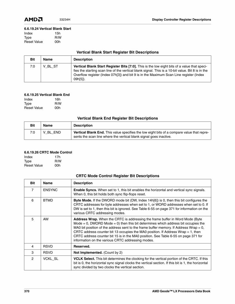
370 AMD Geode™ LX Processors Data Book
Display Controller Register Descriptions33234H
6.6.19.24 Vertical Blank Start
6.6.19.25 Vertical Blank End
6.6.19.26 CRTC Mode Control
Index 15hType R/WReset Value 00h
Vertical Blank Start Register Bit Descriptions
Bit Name Description
7:0 V_BL_ST Vertical Blank Start Register Bits [7:0]. This is the low eight bits of a value that speci-fies the starting scan line of the vertical blank signal. This is a 10-bit value. Bit 8 is in the Overflow register (Index 07h[3]) and bit 9 is in the Maximum Scan Line register (Index 09h[5]).
Index 16hType R/WReset Value 00h
Vertical Blank End Register Bit Descriptions
Bit Name Description
7:0 V_BL_END Vertical Blank End. This value specifies the low eight bits of a compare value that repre-sents the scan line where the vertical blank signal goes inactive.
Index 17hType R/WReset Value 00h
CRTC Mode Control Register Bit Descriptions
Bit Name Description
7 ENSYNC Enable Syncs. When set to 1, this bit enables the horizontal and vertical sync signals. When 0, this bit holds both sync flip-flops reset.
6 BTMD Byte Mode. If the DWORD mode bit (DW, Index 14h[6]) is 0, then this bit configures the CRTC addresses for byte addresses when set to 1, or WORD addresses when set to 0. If DW is set to 1, then this bit is ignored. See Table 6-55 on page 371 for information on the various CRTC addressing modes.
5 AW Address Wrap. When the CRTC is addressing the frame buffer in Word Mode (Byte Mode = 0, DWORD Mode = 0) then this bit determines which address bit occupies the MA0 bit position of the address sent to the frame buffer memory. If Address Wrap = 0, CRTC address counter bit 13 occupies the MA0 position. If Address Wrap = 1, then CRTC address counter bit 15 is in the MA0 position. See Table 6-55 on page 371 for information on the various CRTC addressing modes.
4 RSVD Reserved.
3 RSVD Not Implemented. (Count by 2)
2 VCKL_SL VCLK Select. This bit determines the clocking for the vertical portion of the CRTC. If this bit is 0, the horizontal sync signal clocks the vertical section. If this bit is 1, the horizontal sync divided by two clocks the vertical section.

AMD Geode™ LX Processors Data Book 371
Display Controller Register Descriptions 33234H
Table 6-55 illustrates the various frame buffer addressing schemes. In the table, MAx represents the frame buffer memoryaddress signals, Ax represents the CRTC address counter signals, RSx represents row scan counter output bits. Thebinary value in the column headings is a concatenation of the DWORD Mode and Byte Mode bits. (i.e., {DWORD Mode,ByteMode} in verilog.)
1 SL_RSCBT Select Row Scan Bit. This bit determines which CRTC signal appears on the MA14 address bit sent to the frame buffer memory. If this bit is a 0, bit 1 of the Row Scan counter appears on MA14. If this bit is a 1, then CRTC address counter bit 14, 13, or 12 appears on MA14. See Table 6-55 on page 371 for more information.
0 SL_A13 Select A13. This bit determines which CRTC signal appears on the MA13 address bit sent to the frame buffer memory. If this bit is a 0, bit 0 of the Row Scan counter appears on MA13. If this bit is a 1, then CRTC address counter bit 13, 12, or 11 appears on MA13. See Table 6-55 on page 371 for more information.
Table 6-55. CRTC Memory Addressing Modes
Frame Buffer Memory Address Bit Byte Mode (01) Word Mode (00) DWORD Mode (1X)
MA0 A0 A15 or A13 A12
MA1 A1 A0 A13
MA2 A2 A1 A0
MA3 A3 A2 A1
MA4 A4 A3 A2
MA5 A5 A4 A3
MA6 A6 A5 A4
MA7 A7 A6 A5
MA8 A8 A7 A6
MA9 A9 A8 A7
MA10 A10 A9 A8
MA11 A11 A10 A9
MA12 A12 A11 A10
MA13 A13 or RS0 A12 or RS0 A11 or RS0
MA14 A14 or RS1 A13 or RS1 A12 or RS1
MA15 A15 A14 A13
CRTC Mode Control Register Bit Descriptions (Continued)
Bit Name Description

372 AMD Geode™ LX Processors Data Book
Display Controller Register Descriptions33234H
6.6.19.27 Line Compare
6.6.19.28 CPU Data Latch State
6.6.19.29 Attribute Index/Data FF State
Index 18hType R/WReset Value 00h
Line Compare Register Bit Descriptions
Bit Name Description
7:0 LINE_COMP[7:0] Line Compare Register Bits [7:0]. This value specifies the low eight bits of a compare value that represents the scan line where the CRTC frame buffer address counter is reset to 0. This can be used to create a split screen by using the Start Address registers to specify a non-zero location at which to begin the screen image. The lower portion of the screen (starting at frame buffer address 0) is immune to screen scrolling (and pel panning as specified in the Attribute Mode Control register (Index 10h). Line Compare is a 10-bit value. Bit 8 is located in the Overflow register (Index 07h[4]) and bit 9 is in the Maximum Scan Line register (Index 09h[6]).
Index 22hType ROReset Value 00h
CPU Data Latch State Register Bit Descriptions
Bit Name Description
7:0 DLV Data Latch Value. This read only field returns a byte of the CPU data latches and can be used in VGA save/restore operations. The graphics controller’s Read Map Select field (Index 04h[1:0]) specifies which byte/map (0-3) is returned.
Index 24hType ROReset Value 00h
Attribute Index/Data FF State Register Bit Descriptions
Bit Name Description
7 FFST FF State. This read only bit indicates the state of the attribute controller index/data flip-flop. When this bit is 0, the next write to Index 3C0h will write an index value; when this bit is 1, the next write to Index 3C0h will write a data register value.
6:0 RSVD Reserved.

AMD Geode™ LX Processors Data Book 373
Display Controller Register Descriptions 33234H
6.6.19.30 Attribute Index State
6.6.20 VGA Graphics Controller RegistersThe graphics controller registers are accessed by writing an index value to the Graphics Controller Index register (IndexAddress 3CEh) and reading or writing the register using the Graphics Controller Data register (Data Address 3CFh).
6.6.20.1 VGA Graphics Controller Index
Index 26hType ROReset Value xxh
Attribute Index State Register Bit Descriptions
Bit Name Description
7:6 RSVD Reserved.
5:0 ATT_IN_VA Attribute Index Value. This read only value indicates the value of Attribute Index regis-ter bits [5:0] (Index 3C0h).
Table 6-56. Graphics Controller Registers Summary
Index Type Register Reset Value Reference
-- R/W VGA Graphics Controller Index xxh Page 373
-- R/W VGA Graphics Controller Data xxh Page 374
00h R/W VGA Set/Reset xxh Page 374
01h R/W VGA Enable Set/Reset xxh Page 374
02h R/W VGA Color Compare xxh Page 375
03h R/W VGA Data Rotate xxh Page 375
04h R/W VGA Read Map Select xxh Page 376
05h R/W VGA Graphics Mode xxh Page 376
06h R/W VGA Miscellaneous xxh Page 377
07h R/W VGA Color Don’t Care xxh Page 378
08h R/W VGA Bit Mask xxh Page 378
Index Address 3CEhType R/WReset Value xxh
VGA Graphics Controller Index Register Bit Descriptions
Bit Name Description
7:4 RSVD Reserved.
3:0 INDEX Index.

374 AMD Geode™ LX Processors Data Book
Display Controller Register Descriptions33234H
6.6.20.2 VGA Graphics Controller Data
6.6.20.3 VGA Set/Reset
Bits [3:0] allow bits in their respective maps to be set or reset through write modes 0 or 3. See Section 6.5.5.3 "WriteModes" on page 290 for more information.
6.6.20.4 VGA Enable Set/Reset
Bits [3:0] enable the Set/Reset function for their respective maps in write mode 0. See Section 6.5.5.3 "Write Modes" onpage 290 for more information.
Data Address 3CFhType R/WReset Value xxh
VGA Graphics Controller Data Register Bit Descriptions
Bit Name Description
7:4 RSVD Reserved.
3:0 DATA Data.
Index 00hType R/WReset Value xxh
VGA Set/Reset Register Bits Bit Descriptions
Bit Name Description
7:4 RSVD Reserved.
3 SR_MP3 Set/Reset Map 3.
2 SR_MP2 Set/Reset Map 2.
1 SR_MP1 Set/Reset Map 1.
0 SR_MP0 Set/Reset Map 0
Index 01hType R/WReset Value xxh
VGA Enable Set/Reset Register Bit Descriptions
Bit Name Description
7:4 RSVD Reserved.
3 EN_SR_MP3 Enable Set/Reset Map 3.
2 EN_SR_MP2 Enable Set/Reset Map 2.
1 EN_SR_MP1 Enable Set/Reset Map 1.
0 EN_SR_MP0 Enable Set/Reset Map 0.

AMD Geode™ LX Processors Data Book 375
Display Controller Register Descriptions 33234H
6.6.20.5 VGA Color Compare
Bits [3:0] specify a compare value that allows the CPU to compare pixels in planar modes. Read mode 1 performs a com-parison based on these bits combined with the Color Don’t Care bits. Data returned will contain a 1 in each one of the eightpixel positions where a color match is found. See the description of read modes (Section 6.5.5.4 on page 291) for moreinformation.
6.6.20.6 VGA Data Rotate
Index 02hType R/WReset Value xxh
VGA Color Compare Register Bit Descriptions
Bit Name Description
7:4 RSVD Reserved.
3 CO_CM_MP3 Color Compare Map 3.
2 CO_CM_MP2 Color Compare Map 2.
1 CO_CM_MP1 Color Compare Map 1.
0 CO_CM_MP0 Color Compare Map 0.
Index 03hType R/WReset Value xxh
VGA Data Rotate Bit Descriptions Bit Descriptions
Bit Name Description
7:5 RSVD Reserved.
4:3 WROP Write Operation. Data written to the frame buffer by the CPU can be logically combined with data already in the CPU data latches.
00: Copy (CPU data written unmodified).01: CPU data ANDed with latched data.10: CPU data ORed with latched data.11: CPU data XORed with latched data.
See the description of write modes (Section 6.5.5.3 on page 290) for more information.
2:0 ROTCNT Rotate Count. This value is used to rotate the CPU data before it is used in write modes 0 and 3. The CPU data byte written is rotated right, with low bits wrapping to the high bit positions. See the description of write modes (Section 6.5.5.3 on page 290) for more information.

376 AMD Geode™ LX Processors Data Book
Display Controller Register Descriptions33234H
6.6.20.7 VGA Read Map Select
6.6.20.8 VGA Graphics Mode
Index 04hType R/WReset Value xxh
VGA Read Map Select Register Bit Descriptions
Bit Name Description
7:2 RSVD Reserved.
1:0 R_MP_SL Read Map Select. This field specifies which map CPU read data is taken from in read mode 0. In Odd/Even modes (specified by the Odd/Even bit in the Graphics Mode regis-ter, Index 05h[4]) bit 1 of this field specifies which pair of maps returns data.
When bit 1 is 0, data is returned from maps 0 and 1. When bit 1 is 1, data is returned from maps 2 and 3. The CPU read address bit A0 determines which byte is returned (low or high) in Odd/Even modes. In non-Odd/Even modes, these bits (both bits [1:0]) specify the map to read (0, 1, 2, or 3) and the CPU accesses data sequentially within the speci-fied map.
Index 05hType R/WReset Value xxh
VGA Graphics Mode Register Bit Descriptions
Bit Name Description
7 RSVD Reserved.
6 256_CM 256 Color Mode. When set to a 1, this bit configures the video serializers in the graphics controller for the 256 color mode (BIOS mode 13h). When this bit is 0, the Shift Register Mode bit (bit 5) controls the serializer configuration.
5 SH_R_MD Shift Register Mode. When set to a 1, this bit configures the video serializers for BIOS modes 4 and 5. When this bit is 0, the serializers are taken in parallel (i.e., configured for 4-bit planar mode operation).
Note that the serializers are also wired together serially so that map 3 bit 7 feeds map 2 bit 0, map 2 bit 7 feeds map 1 bit 0, and map 1 bit 7 feeds map 0 bit 0. This allows for a 32-pixel 1 bit-per-pixel serializer to be used. For this configuration, color planes 1, 2, and 3 should be masked off using the Color Plane Enable register (Attribute Controller, Index 12h, on page 381.)
4 ODD_EVEN Odd/Even. When this bit is set to 1, CPU address bit A0 will select between maps 0 and 1 or maps 2 and 3 depending on the state of the Read Map Select field (Index 04h[1:0]). When this bit is 0, the CPU accesses data sequentially within a map. This bit is equiva-lent to the Odd/Even bit in the VGA Miscellaneous register (Index 06h[2]), but is inverted in polarity from that bit.
3 RD_MD Read Mode. This bit determines what is returned to the CPU when it reads the frame buffer. When this bit is 1, the result of a color compare operation is returned. The eight bits in the CPU read data contain a 1 in each pixel position where the color compare operation was true, and a 0 where the operation was false. When this bit is 0, frame buffer map data is returned.
2 RSVD Reserved.
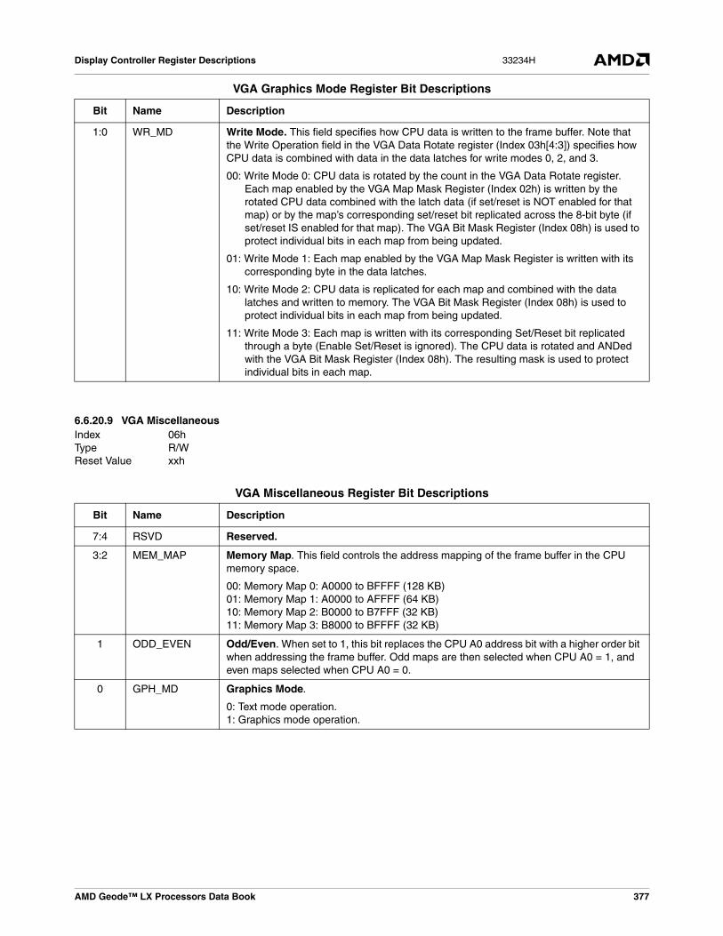
AMD Geode™ LX Processors Data Book 377
Display Controller Register Descriptions 33234H
6.6.20.9 VGA Miscellaneous
1:0 WR_MD Write Mode. This field specifies how CPU data is written to the frame buffer. Note that the Write Operation field in the VGA Data Rotate register (Index 03h[4:3]) specifies how CPU data is combined with data in the data latches for write modes 0, 2, and 3.
00: Write Mode 0: CPU data is rotated by the count in the VGA Data Rotate register. Each map enabled by the VGA Map Mask Register (Index 02h) is written by the rotated CPU data combined with the latch data (if set/reset is NOT enabled for that map) or by the map’s corresponding set/reset bit replicated across the 8-bit byte (if set/reset IS enabled for that map). The VGA Bit Mask Register (Index 08h) is used to protect individual bits in each map from being updated.
01: Write Mode 1: Each map enabled by the VGA Map Mask Register is written with its corresponding byte in the data latches.
10: Write Mode 2: CPU data is replicated for each map and combined with the data latches and written to memory. The VGA Bit Mask Register (Index 08h) is used to protect individual bits in each map from being updated.
11: Write Mode 3: Each map is written with its corresponding Set/Reset bit replicated through a byte (Enable Set/Reset is ignored). The CPU data is rotated and ANDed with the VGA Bit Mask Register (Index 08h). The resulting mask is used to protect individual bits in each map.
Index 06hType R/WReset Value xxh
VGA Miscellaneous Register Bit Descriptions
Bit Name Description
7:4 RSVD Reserved.
3:2 MEM_MAP Memory Map. This field controls the address mapping of the frame buffer in the CPU memory space.
00: Memory Map 0: A0000 to BFFFF (128 KB)01: Memory Map 1: A0000 to AFFFF (64 KB)10: Memory Map 2: B0000 to B7FFF (32 KB)11: Memory Map 3: B8000 to BFFFF (32 KB)
1 ODD_EVEN Odd/Even. When set to 1, this bit replaces the CPU A0 address bit with a higher order bit when addressing the frame buffer. Odd maps are then selected when CPU A0 = 1, and even maps selected when CPU A0 = 0.
0 GPH_MD Graphics Mode.
0: Text mode operation.1: Graphics mode operation.
VGA Graphics Mode Register Bit Descriptions
Bit Name Description
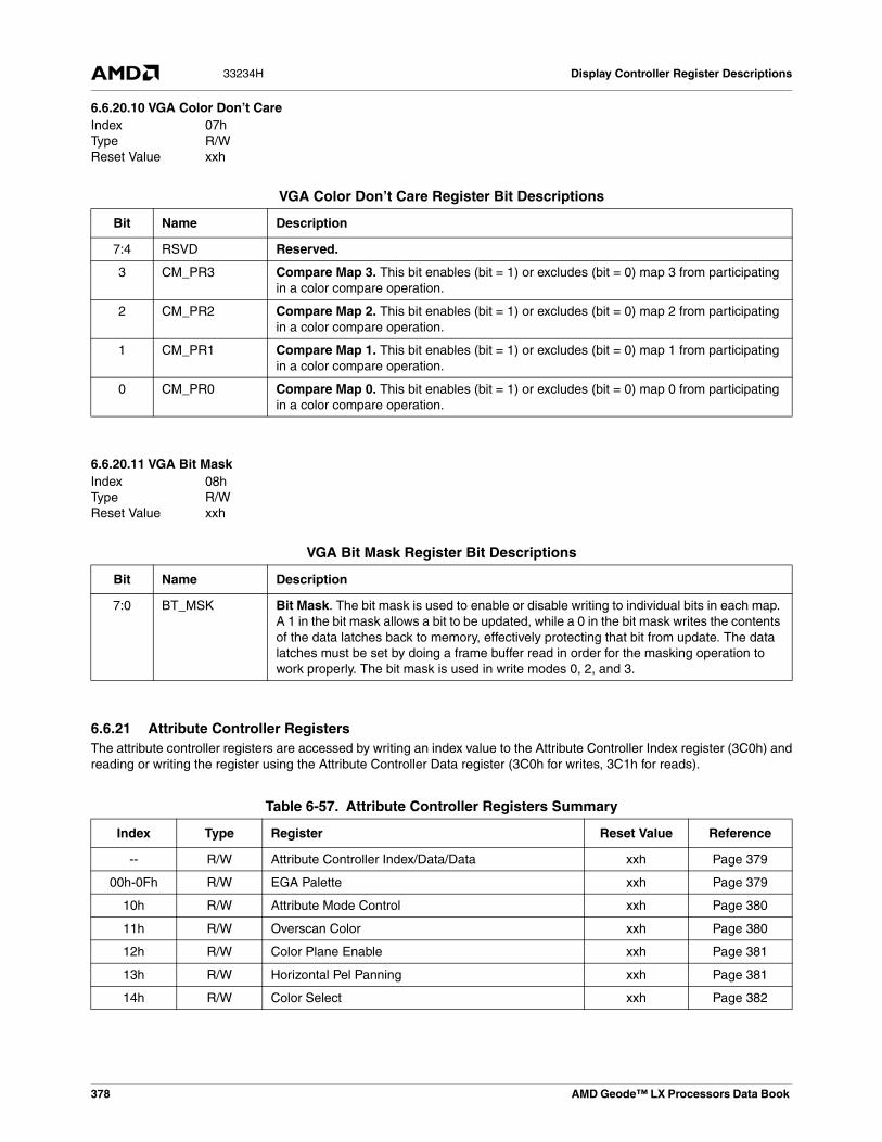
378 AMD Geode™ LX Processors Data Book
Display Controller Register Descriptions33234H
6.6.20.10 VGA Color Don’t Care
6.6.20.11 VGA Bit Mask
6.6.21 Attribute Controller RegistersThe attribute controller registers are accessed by writing an index value to the Attribute Controller Index register (3C0h) andreading or writing the register using the Attribute Controller Data register (3C0h for writes, 3C1h for reads).
Index 07hType R/WReset Value xxh
VGA Color Don’t Care Register Bit Descriptions
Bit Name Description
7:4 RSVD Reserved.
3 CM_PR3 Compare Map 3. This bit enables (bit = 1) or excludes (bit = 0) map 3 from participating in a color compare operation.
2 CM_PR2 Compare Map 2. This bit enables (bit = 1) or excludes (bit = 0) map 2 from participating in a color compare operation.
1 CM_PR1 Compare Map 1. This bit enables (bit = 1) or excludes (bit = 0) map 1 from participating in a color compare operation.
0 CM_PR0 Compare Map 0. This bit enables (bit = 1) or excludes (bit = 0) map 0 from participating in a color compare operation.
Index 08hType R/WReset Value xxh
VGA Bit Mask Register Bit Descriptions
Bit Name Description
7:0 BT_MSK Bit Mask. The bit mask is used to enable or disable writing to individual bits in each map. A 1 in the bit mask allows a bit to be updated, while a 0 in the bit mask writes the contents of the data latches back to memory, effectively protecting that bit from update. The data latches must be set by doing a frame buffer read in order for the masking operation to work properly. The bit mask is used in write modes 0, 2, and 3.
Table 6-57. Attribute Controller Registers Summary
Index Type Register Reset Value Reference
-- R/W Attribute Controller Index/Data/Data xxh Page 379
00h-0Fh R/W EGA Palette xxh Page 379
10h R/W Attribute Mode Control xxh Page 380
11h R/W Overscan Color xxh Page 380
12h R/W Color Plane Enable xxh Page 381
13h R/W Horizontal Pel Panning xxh Page 381
14h R/W Color Select xxh Page 382

AMD Geode™ LX Processors Data Book 379
Display Controller Register Descriptions 33234H
6.6.21.1 Attribute Controller Index/Data
The attribute controller registers do not have a separate address for writing index and data information. Instead, an internalflip-flop alternates between index and data registers. Reading Input Status Register 1 (3BAh or 3DAh) clears the flip-flop tothe index state. The first write to 3C0h following a read from Input Status Register 1 will update the index register. The nextwrite will update the selected data register. The next write specifies a new index, etc.
6.6.21.2 EGA Palette
Index Address 3C0hData Address 3C1h (R)
3C0h (W)Type R/WReset Value xxh
Attribute Controller Index Register Bit Descriptions
Bit Name Description
7:6 RSVD Reserved.
5 INT_PAL_AD Internal Palette Address. This bit determines whether the EGA palette is addressed by the video pixel stream (bit = 1) or by the Attribute Controller Index register (bit = 0). This bit should be set to 1 for normal VGA operation. CPU I/O accesses to the palette are dis-abled unless this bit is a 0.
4:0 DATA_RG_INX Data Register Index. This field addresses the individual palette and data registers.
Index 00h-0FhType R/WReset Value xxh
EGA Palette Register Bit Descriptions
Bit Name Description
7:6 RSVD Reserved.
5:0 COL_VAL Color Value. Each of these 16 registers is used to expand the pixel value from the frame buffer (one, two, or four bits wide) into a 6-bit color value that is sent the video DAC. The EGA palette is “programmed out of the way” in 256 color mode. These registers can only be read or written when the Internal Palette Address bit in the Index register (3C0h) is 0.

380 AMD Geode™ LX Processors Data Book
Display Controller Register Descriptions33234H
6.6.21.3 Attribute Mode Control
6.6.21.4 Overscan Color
Index 10hType R/WReset Value xxh
Attribute Mode Control Register Bit Descriptions
Bit Name Description
7 P5:4_SEL P5:4 Select. When this bit is a 1, bits [5:4] of the 8-bit VGA pixel value are taken from bits [1:0] of the Color Select register (Index 14h). When a 0, bits [5:4] of the pixel are taken from bits [5:4] of the EGA palette output.
6 PEL_W Pel Width. This bit is used in 256 color mode to shift four pixels through the attribute controller for each character clock. Clearing this bit shifts eight pixels for each charac-ter clock.
5 PEL_PAN_COMP Pel Panning Compatibility. When this bit is a 1, the scan lines following a line com-pare are immune to the effects of the pel panning. When this bit is a 0, the entire screen is affected by pel panning, regardless of the line compare operation.
4 RSVD Reserved.
3 EN_BLINK Enable Blink. When this bit is a 1, attribute bit 7 is used to cause a character to blink (bit 7 = 1) or not (bit 7 = 0). When this bit is 0, attribute bit 7 is used as a background intensity bit.
2 EN_LGC Enable Line Graphics Codes. When this bit is 0, the 9th Dot in 9-wide character modes is always set to the background color. When this bit is 1, the 9th Dot is equal to the foreground color for character codes C0h-DFh, which are the line graphics charac-ter codes.
1 MON_EMU Monochrome Emulation. When this bit is a 1, the underline in 9-Dot mode extends for all nine Dots and an underlined phrase will have a continuous line under it. When this bit is 0, the underline is only active for eight Dots, and an underlined phrase will have a broken line under it.
0 GR_MODE Graphics Mode. When this bit is 1, graphics mode is selected and pixel data from the frame buffer is used to produce the pixel stream. When this bit is 0, text mode is selected, and text attribute and font pattern information is used to produce the pixel stream.
Index 11hType R/WReset Value xxh
Overscan Color Register Bit Descriptions
Bit Name Description
7:0 OVER_COLOR Overscan Color. This value is output as the pixel value to the video DAC when the Dis-play Enable signal from the CRTC is inactive.
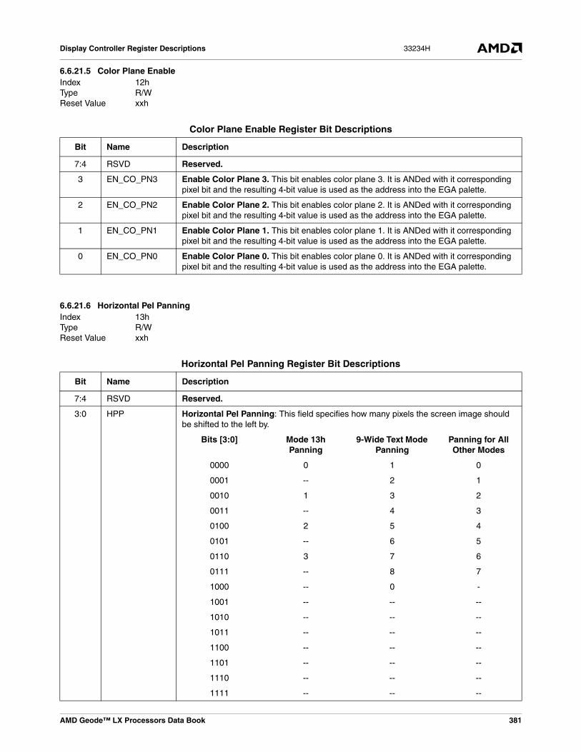
AMD Geode™ LX Processors Data Book 381
Display Controller Register Descriptions 33234H
6.6.21.5 Color Plane Enable
6.6.21.6 Horizontal Pel Panning
Index 12hType R/WReset Value xxh
Color Plane Enable Register Bit Descriptions
Bit Name Description
7:4 RSVD Reserved.
3 EN_CO_PN3 Enable Color Plane 3. This bit enables color plane 3. It is ANDed with it corresponding pixel bit and the resulting 4-bit value is used as the address into the EGA palette.
2 EN_CO_PN2 Enable Color Plane 2. This bit enables color plane 2. It is ANDed with it corresponding pixel bit and the resulting 4-bit value is used as the address into the EGA palette.
1 EN_CO_PN1 Enable Color Plane 1. This bit enables color plane 1. It is ANDed with it corresponding pixel bit and the resulting 4-bit value is used as the address into the EGA palette.
0 EN_CO_PN0 Enable Color Plane 0. This bit enables color plane 0. It is ANDed with it corresponding pixel bit and the resulting 4-bit value is used as the address into the EGA palette.
Index 13hType R/WReset Value xxh
Horizontal Pel Panning Register Bit Descriptions
Bit Name Description
7:4 RSVD Reserved.
3:0 HPP Horizontal Pel Panning: This field specifies how many pixels the screen image should be shifted to the left by.
Bits [3:0] Mode 13h Panning
9-Wide Text Mode Panning
Panning for All Other Modes
0000 0 1 0
0001 -- 2 1
0010 1 3 2
0011 -- 4 3
0100 2 5 4
0101 -- 6 5
0110 3 7 6
0111 -- 8 7
1000 -- 0 -
1001 -- -- --
1010 -- -- --
1011 -- -- --
1100 -- -- --
1101 -- -- --
1110 -- -- --
1111 -- -- --

382 AMD Geode™ LX Processors Data Book
Display Controller Register Descriptions33234H
6.6.21.7 Color Select
6.6.22 Video DAC RegistersVideo DAC palette registers are accessed by writing the Palette Address register at the read or write address, then perform-ing three reads or writes, one for each of the red, green, and blue color values. The video DAC provides an address incre-ment feature that allows multiple sets of color triplets to be read or written without writing the Palette Address register again.To invoke this feature, simply follow the first triplet read/write with the next triplet read/write.
The original IBM video DAC behavior for read operations is:
1) CPU initiates a palette read by writing INDEX to I/O address 3C7h.
2) Video DAC loads a temporary register with the value stored at palette[INDEX].
3) Video DAC increments INDEX (INDEX = INDEX + 1).
4) CPU reads red, green, blue color values from temporary register at I/O address 3C9h.
5) Loop to step 2.
The original IBM video DAC behavior for write operations is:
1) CPU initiates a palette write by writing INDEX to I/O address 3C8h.
2) CPU writes red, green, blue color values to temporary DAC registers at I/O address 3C9h.
3) Video DAC stores the temporary register contents in palette[INDEX].
4) Video DAC increments INDEX (INDEX = INDEX + 1).
5) Loop to step 2.
Index 14hType R/WReset Value xxh
Color Select Register Bit Descriptions
Bit Name Description
7:4 RSVD Reserved.
3:2 P[7:6] P7 and P6. These bits are used to provide the upper two bits of the 8-bit pixel value sent to the video DAC in all modes except the 256 color mode (mode 13h).
1:0 P[5:4] P5 and P4. These bits are used to provide bits 5 and 4 of the 8-bit pixel value sent to the video DAC when the P5:4 Select bit is set in the Attribute Mode Control register (Index 10h[7]). In this case, they replace bits [5:4] coming from the EGA palette.
Table 6-58. Video DAC Registers Summary
I/O Address Type Register Reset Value Reference
3C8h RO Palette Address (Write Mode) 00h Page 383
3C7h RO Palette Address (Read Mode) 00h Page 383
3C7h RO DAC State 00h Page 383
3C9h R/W Palette Data 00h Page 380
3C6h R/W Pel Mask 00h Page 380
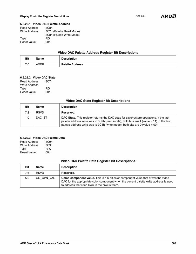
AMD Geode™ LX Processors Data Book 383
Display Controller Register Descriptions 33234H
6.6.22.1 Video DAC Palette Address
6.6.22.2 Video DAC State
6.6.22.3 Video DAC Palette Data
Read Address 3C8hWrite Address 3C7h (Palette Read Mode)
3C8h (Palette Write Mode)Type ROReset Value 00h
Video DAC Palette Address Register Bit Descriptions
Bit Name Description
7:0 ADDR Palette Address.
Read Address 3C7hWrite Address --Type ROReset Value 00h
Video DAC State Register Bit Descriptions
Bit Name Description
7:2 RSVD Reserved.
1:0 DAC_ST DAC State. This register returns the DAC state for save/restore operations. If the last palette address write was to 3C7h (read mode), both bits are 1 (value = 11). If the last palette address write was to 3C8h (write mode), both bits are 0 (value = 00).
Read Address 3C9hWrite Address 3C9hType R/WReset Value 00h
Video DAC Palette Data Register Bit Descriptions
Bit Name Description
7:6 RSVD Reserved.
5:0 CO_CPN_VAL Color Component Value. This is a 6-bit color component value that drives the video DAC for the appropriate color component when the current palette write address is used to address the video DAC in the pixel stream.

384 AMD Geode™ LX Processors Data Book
Display Controller Register Descriptions33234H
6.6.22.4 Video DAC Palette Mask
6.6.23 VGA Block Extended RegistersThe Extended registers are accessed by writing an index value to the CRTC Index register (3B4h or 3D4h) and reading orwriting the register using the CRTC Data register (3B5h or 3D5h). See the description of the I/O Address Select bit in theSection 6.6.17.1 "VGA Miscellaneous Output" on page 356 for more information on the I/O address of the CRTC registers.
Read Address 3C6hWrite Address 3C6hType R/WReset Value 00h
Video DAC Palette Mask Register Bit Descriptions
Bit Name Description
7:0 PAL_MSK Palette Mask. These bits enable their respective color bits between the final VGA 8-bit pixel output and the DAC palette. The bits are ANDed with the incoming VGA pixel value and the result used to address the palette RAM.
Table 6-59. Extended Registers Summary
Index Type Register Reset Value Reference
0030h R/W ExtendedRegisterLock FFh Page 385
043h R/W (Note 1)
Note 1. R/W when unlocked, RO otherwise (see Section 6.6.23.1 "ExtendedRegisterLock" for details).
ExtendedModeControl 00h Page 385
044h R/W (Note 1)
ExtendedStartAddress 00h Page 385
047h R/W (Note 1)
WriteMemoryAperture 00h Page 386
048h R/W (Note 1)
ReadMemoryAperture 00h Page 386
060h R/W (Note 1)
BlinkCounterCtl (for Sim/Test) 00h Page 386
061h R/W (Note 1)
BlinkCounter (for Sim/Test) 00h Page 387
070h R/W (Note 1)
VGALatchSavRes 00h Page 387
071h R/W (Note 1)
DACIFSavRes 00h Page 387

AMD Geode™ LX Processors Data Book 385
Display Controller Register Descriptions 33234H
6.6.23.1 ExtendedRegisterLock
6.6.23.2 ExtendedModeControl
6.6.23.3 ExtendedStartAddress
CRTC Index 030hType R/WReset Value FFh
ExtendedRegisterLock Register Bit Descriptions
Bit Name Description
7:0 LOCK Lock. A value of 4Ch unlocks the extended registers. Any other value locks the extended registers so they are read only. If the extended registers are currently locked, a read to this register will return FFh. If they are unlocked, a read will return 0.
CRTC Index 043hType R/WReset Value 00h
ExtendedModeControl Register Bit Descriptions
Bit Name Description
7:3 RSVD Reserved.
2:1 VG_RG_MAP DC Register Mapping. These bits determine the DC register visibility within the standard VGA memory space (A0000h-BFFFFh). Note that the VGA address space control bits override this feature. If the Miscellaneous Output register RAM Enable bit is 0, all VGA memory space is disabled. Or, if the Memory Map bits of the Graphics Miscellaneous register are set the same as these bits, then the VGA frame buffer memory will appear in this space instead of the GUI registers.
00: Disabled01: A0000h10: B0000h11: B8000h
0 PACK_CH4 Packed Chain4: When this bit is set, the chain4 memory mapping will not skip DWORDs as in true VGA. Host reads and writes to frame buffer DWORDs are contiguous. When this bit is 0, host accesses behave normally and access 1 DWORD out of every 4. Note that this bit has no effect on the VGA display refresh activity. This bit is only intended to provide a front end for packed SVGA modes being displayed by DC.
CRTC Index 044hType R/WReset Value 00h
ExtendedStartAddress Register Bit Descriptions
Bit Name Description
7:6 RSVD Reserved.
5:0 ST_AD_RG[21:16]
Start Address Register Bits [21:16]. Start Address Register Bits [23:18]: These bits extend the VGA start address to 24 bits. Bits [17:10] are in Start Address Hi (Index 0Ch), and bits [9:2] are in Start Address Lo (Index 0Ch).

386 AMD Geode™ LX Processors Data Book
Display Controller Register Descriptions33234H
6.6.23.4 WriteMemoryAperture
6.6.23.5 ReadMemoryAperture
6.6.23.6 BlinkCounterCtl
This register is for simulation and test only.
CRTC Index 047hType R/WReset Value 00h
WriteMemoryAperture Register Bit Descriptions
Bit Name Description
7:0 WR_BASE WriteBase. Offset added to the graphics memory base to specify where VGA write oper-ations start. This value provides DWORD address bits [21:14] when mapping host VGA writes to graphics memory. This allows the VGA base address to start on any 64 KB boundary within the 8 MB of graphics memory.
CRTC Index 048hType R/WReset Value 00h
ReadMemoryAperture Register Bit Descriptions
Bit Name Description
7:0 RD_BASE ReadBase. Offset added to the graphics memory base to specify where VGA read oper-ations start. This value provides DWORD address bits [21:14] when mapping host VGA reads to graphics memory. This allows the VGA base address to start on any 64 KB boundary within the 8 MB of graphics memory.
CRTC Index 060hType R/WReset Value 00h
BlinkCounterCtl Register Bit Descriptions
Bit Name Description
7 HLD_CNT Hold Count. When set, prevents the blink counter from incrementing with each leading edge VSYNC.
6:5 RSVD Reserved.
4:0 BLNK_CNT Blink Count. The blink counter is loaded with this value while the Sequencer Reset reg-ister is in the reset state.

AMD Geode™ LX Processors Data Book 387
Display Controller Register Descriptions 33234H
6.6.23.7 BlinkCounter
This register is for simulation and test only.
6.6.23.8 VGALatchSavRes
6.6.23.9 DACIFSavRes
CRTC Index 061hType ROReset Value 00h
BlinkCounter Register Bit Descriptions
Bit Name Description
7:5 RSVD Reserved.
4:0 BLNK_CNT Blink Count. These bits provide a real-time blink counter value. This register is not syn-chronized to the system clock domain.
CRTC Index 070hType R/WReset Value 00h
VGALatchSavRes Register Bit Descriptions
Bit Name Description
7:0 VGA_LSR VGALatchSavRes. This register is used to save/restore the 32-bit VGA data latch. When the CRTC index register is written, an internal byte counter is cleared to 0. Four successive reads or writes to the CRTC data register at this index will return or write bytes 0 (bits [7:0]), 1 (bits [15:8]), 2 (bits [23:16]), then 3 (bits [31:24]) in sequence.
CRTC Index 071hType R/WReset Value 00h
DACIFSavRes Register Bit Descriptions
Bit Name Description
7:0 DACIFSR DACIFSavRes. This register is used to save/restore the VGA palette interface logic state. When the CRTC index register is written, an internal byte counter is cleared to 0. Four successive reads or writes to the CRTC data register at this index will return or write bytes 0 (bits [7:0]), 1 (bits [15:8]), 2 (bits [23:16]), then 3 (bits [31:24]) in sequence.