a leakage-inductance-tolerant commutation …eprints.nottingham.ac.uk/53510/1/a...
TRANSCRIPT

JESTPE-2017-10-0713.R2
1
Abstract— This paper proposes a generalised commutation
strategy suitable for matrix-based isolated AC/AC conversion stages in Solid State Transformers for use whenever there is non-negligible leakage inductance in the isolation transformer. The standard 4-step commutation used in matrix converters can no longer be applied when transformer leakage inductance is present, as overrated switching devices or dissipative snubbers would be necessary, reducing the attractiveness of the topologies that include matrix-based isolated AC/AC stages. A case study of a single-phase AC/AC converter has been investigated in detail to demonstrate the application of the proposed commutation method to a topology that has recently been identified as the potential building block for future multi-modular AC/AC converters for grid applications. The proposed leakage-inductance-tolerant commutation strategy is based on the definition of a current decoupling phase in the commutation sequence and only needs suitable timing of the commutation steps, without high bandwidth voltage or current measurements. Matching simulations and experimental results from a 3kW laboratory scale prototype are presented to support the effectiveness of the proposed strategy.
Index Terms—4-Step Commutation, Grid interconnection, Isolated Single-Phase AC-AC converters, Leakage-inductance, Matrix converters, Multi-Modular converters, Solid-State Transformers
I. INTRODUCTION
N recent years, considerable research efforts have been directed toward power-electronic based solutions to replace
low-frequency transformers in LV and MV distribution grids as well as in traction systems, both for AC/AC and AC/DC conversion [1, 2]. Transformer volume and weight are critical when space is restricted or expensive, e.g. in city centers [3] or in locomotives [4]. In these cases, power density can be increased using converters with medium-frequency isolation stages [3-5]. Despite a large diversity of ratings, applications and topologies, these solutions are referred to generically as Solid State Transformers (SSTs). SSTs are still a developing technology and no broad consensus has been reached yet on their functional requirements. A first observation is that mass and volume reduction offered by SSTs tend to be counterbalanced by their higher cost and complexity, lower efficiency and reliability and by their lower overload capability
Manuscript received October 30, 2017; revised May 18, 2018. This work is
supported by the Newton Picarte and Fondecyt Project Grant 1160690. U. Nasir, A. Costabeber, P. Wheeler and J. Clare are associated with Power
Electronics & Machine Control (PEMC) research group at The University of Nottingham, Nottingham NG7 2RD, U.K. (e-mail:
[3]. Therefore, replacing low-frequency transformers with SSTs in existing applications would not necessarily lead to a technical and financial success. On the contrary, SSTs can be better deployed in dedicated scenarios where advantages can be exploited, and limitations can be mitigated, based on system level design considerations. The opportunity to shape these scenarios for SSTs comes, for example, from future distribution systems [6] and new traction systems [5, 7].
Ideally, SSTs should provide isolation enhanced by the controllability of power converters. The SST should decouple the load from power system perturbations, e.g. provide high quality load voltage waveforms in presence of grid voltage harmonics, sags, imbalances and faults [2], as well as decouple the power system from the load behaviour, e.g. draw from the grid sinusoidal and balanced currents with unity or controllable power factor [3] in presence of load imbalance and/or non-linearity and regardless the load power factor. Several topologies [1] have been proposed for SSTs, with different capabilities. A simplistic distinction can be made between the fully matrix-based SSTs in Fig. 1(a), without energy storage and hence with potentially smaller footprint, the voltage-source ones (e.g. DAB based) with energy storage and the hybrid solutions shown in Fig. 1(b) with a combination of voltage-source and matrix-based stages. If energy storage is available, the grid-load decoupling functionalities discussed above can be inherently achieved. Instead, in a direct converter the need for
[email protected]; [email protected]; [email protected]; [email protected]).
M. Rivera is with the Department of Electrical Engineering, Universidad de Talca, Curico, PB, 3341717 chile (e-mail: [email protected]).
A Leakage-Inductance-Tolerant Commutation Strategy for Isolated AC/AC Converters
Usman Nasir, Student Member, IEEE, Alessandro Costabeber, Member, IEEE, Marco Rivera, Member, IEEE, Pat Wheeler, Senior Member, IEEE, and Jon Clare, Senior Member, IEEE
I
(a)
(b)
Fig. 1 Solid State Transformer (SST) architectures with matrix-based isolation stages: (a) direct and (b) with energy storage
Converter 2Converter 1
MF/HF AC Link
AC Grid
2
AC Grid
1
DC LinkMF/HF
AC Link
AC Grid
1
AC Grid
2
Converter 1 Converter 2

JESTPE-2017-10-0713.R2
2
matching input and output instantaneous powers can lead to a drastic reduction of the control capabilities, especially under unbalanced operation and faults on the grid or load side. However, in specific non-critical applications the higher power density can be prioritized, sacrificing functionality. A recent example that could benefit from a direct converter is the mid-feeder compensator for LV distribution grids discussed in [8].
Whenever the SST presents a matrix-based stage coupled to a MF transformer, such as in [8-10], the commutation process becomes challenging in presence of non-negligible transformer leakage inductance since no free-wheeling path is available. The aim of this paper is not to focus on a specific SST topology but rather to provide a methodology to enhance the commutation process of a family of matrix-based or hybrid converters shown in Fig. 1. The fundamental assumption behind the commutation process in matrix topologies is that one side of the converter can be considered a voltage source and the other a current source during commutation. Adding a leakage inductance in the AC link causes potential current mismatches during commutation that must be adequately managed to minimise the impact on the converter operation and design. Although interleaved windings can be used to reduce the leakage inductance, in practical applications it is not always possible to have adequate control over the leakage, due to cost or other system design constraints.
A current based 4-step commutation sequence for the SST in Fig. 1(b) was proposed in [9] but the drawback of the proposed solution is that the impact of transformer leakage inductance on the commutation process was neglected, thus it relies on negligible transformer leakage to successfully complete commutation. To date, various methods have been reported in the literature to deal with the leakage energy. For instance, employing snubber circuits can help to mitigate the issue [11] but at the cost of increased power losses and reduced power density. The snubber capacitors can also cause turn-on loss in the switches, as the energy of the capacitor is dissipated in the switching device and an auxiliary biasing circuit would be required to mitigate the issue [12]. A second approach can be the introduction of a capacitor at the primary side of the transformer, forming a parallel-resonant tank with the magnetisation inductance [13]. This approach achieves soft-switching but the leakage energy is dissipated in the transformer winding resistance and tuning of the resonant tank can be challenging. Reference [14] utilises a capacitor in series with the leakage inductance which forms a series-resonant tank. A common drawback of all the discussed methods is that they require additional energy storage components to target the commutation issue. An alternative method to deal with commutation in the presence of leakage inductance could be to drive the commutation by using a controllable voltage source. This method does not need additional energy storage components and can also avoid resonance related problems. The source-based commutation of a single-phase DC/AC converter presented in [15] achieves complete soft-switching of the cyclo-converter but it does not take into account the effect of the leakage inductance.
Other existing research into matrix-based SST topologies
pay limited attention to the impact of the leakage inductance on the commutation process. Recently, the importance of accounting for the leakage effect has been highlighted for a MF/HF isolated three phase to three phase direct converter [16], showing how the conventional 4-step commutation strategy must be substantially reviewed to avoid over voltage across the semiconductor devices. However, a generalised concept to deal with the leakage energy, suitable for all SSTs with matrix-based stages, has not been clearly addressed in the literature.
This paper proposes a new generalised commutation concept, which provides safe commutation by naturally recirculating the energy stored in the leakage inductance. As a case study, the proposed concept is applied in detail to a single-phase isolated AC/AC converter and experimentally validated on a 3kW rig. The only requirement of the strategy is suitable timing of the commutation steps, like the 4-step commutation used in Matrix Converters. No fast or time-critical voltage or current measurements are required to implement the proposed commutation. The specific case study has been chosen considering the potential use of the matrix-based single-phase SST topology as the fundamental building block for a new breed of multi-modular power converter architectures for grid connected applications [17]. These new concepts will combine the advantages of an SST with those of a modular, flexible and scalable structure which can be adapted to different voltage levels and frequencies.
The proposed commutation concept is based on the introduction of an intermediate state, named the current decoupling phase, during which the leakage inductance current is modified, driven by the input voltage or by a modulated version of it, to bring its sign and magnitude to the new value required after commutation without requiring snubbers or clamps. The application of the proposed concept to a minimal circuit is briefly discussed in section II, to highlight the simplicity and generality of the method. The specific case study of a single-phase isolated AC-AC converter is discussed in detail and experimentally validated in the remaining sections.
II. BASIC PRINCIPLE OF THE LEAKAGE-INDUCTANCE-TOLERANT COMMUTATION STRATEGY
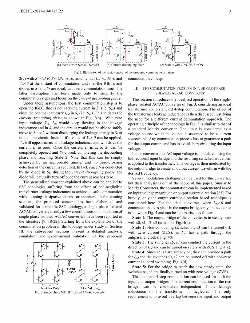
As mentioned in the previous section, the basic concept of the proposed leakage-inductance-tolerant commutation strategy relies on the introduction of a current decoupling phase that enables manipulation of the leakage inductance current in order to match the sign and magnitude imposed by the output current after commutation. To illustrate the basic idea, consider the minimal circuit shown in Fig. 2. It is assumed that the converter has a voltage source at the input and a current source at the output, represented by the filter inductor Lo. The filter inductor is much larger than the leakage inductance, i.e. Lo>>Lleak, so that during commutation the leakage inductance current can be modified while the output current remains nearly constant. In this simple and general example, the input voltage comes from a previous stage of the converter, from an independent voltage source or from a controllable voltage source.
Consider now the case where the circuit has to commutate from State 1 in Fig. 2(a) with S1=ON, S2=OFF to State 2 in Fig.
JESTPE-2017-10-0713.R2
3
2(c) with S1=OFF, S2=ON. Also, assume that Iout>0, IL>0 and Vin<0 at the instant of commutation and that the IGBTs and diodes in S1 and S2 are ideal, with zero commutation time. The latter assumption has been made only to simplify the commutation steps and focus on the current decoupling phase.
Under these assumptions, the first commutation step is to open the IGBT that is not carrying current in S1 (i.e. S1n) and close the one that can carry Iout in S2 (i.e. S2n). This initiates the current decoupling phase as shown in Fig. 2(b). With zero input voltage Vin, Iout would keep flowing in the leakage inductance and in S1 and the circuit would not be able to safely move to State 2 without discharging the leakage energy in S1 or in a clamp circuit. Instead, if a value of Vin<0 can be applied, Vin will appear across the leakage inductance and will drive the current IL to zero. Once the current IL is zero, S1 can be completely opened and S2 closed, completing the decoupling phase and reaching State 2. Note that this can be simply achieved by an appropriate timing, and no zero-crossing detection of the current is required. In fact, since IL is conducted by the diode in S1n during the current decoupling phase, the diode will naturally turn off once the current reaches zero.
The generalised concept explained above can be applied to SST topologies suffering from the effect of non-negligible transformer leakage inductance to achieve a safe-commutation without using dissipative clamps or snubbers. In the coming sections, the proposed concept has been elaborated and validated for a specific SST topology, a single-phase isolated AC/AC converter, as only a few contributions on modulation of single phase isolated AC/AC converters have been reported in the literature [9, 18-22]. Starting from the explanation of the commutation problem in the topology under study in Section III, the subsequent sections present a detailed analysis, simulation and experimental validation of the proposed
commutation concept.
III. THE COMMUTATION PROBLEM IN A SINGLE-PHASE
ISOLATED AC/AC CONVERTER
This section introduces the idealised operation of the single-phase isolated AC/AC converter of Fig. 3, considering an ideal transformer and a standard 4-step commutation. The effect of the transformer leakage inductance is then discussed, justifying the need for a different current commutation approach. The operating principle of the topology in Fig. 3 is similar to that of a standard Matrix converter. The input is considered as a voltage source while the output is assumed to be a current source/sink. Any commutation process has to guarantee a path for the output current and has to avoid short-circuiting the input voltage.
In this converter, the AC input voltage is modulated using the bidirectional input bridge and the resulting switched waveform is applied to the transformer. This voltage is then modulated by the output bridge to create an output current waveform with the desired frequency.
Several modulation strategies can be used for this converter, but their analysis is out of the scope of this paper. Similar to Matrix Converters, the commutation can be implemented based on input voltage magnitude or output current direction [23]. For brevity, only the output current direction based technique is considered here. For the ideal converter, when Iout>0 and commutation takes place in the output bridge only, the sequence is shown in Fig. 4 and can be summarised as follows:
State 1: The output bridge of the converter is in steady state with s0, s1, s2, s3 turned on. Fig. 4(a).
State 2: Non-conducting switches s1, s3 can be turned off, with zero current (ZCS), as Iout has a path through the antiparallel diodes. Fig. 4(b).
State 3: The switches s5, s7 can conduct the current in the direction of Iout and can be turned on safely with ZCS. Fig. 4(c).
State 4: Since s5, s7 are already on, they can provide a path for Iout and the switches s0, s2 can be turned off with non-zero current i.e. hard switching. Fig. 4(d).
State 5: For the bridge to reach the new steady state, the switches s4, s6 are finally turned on with zero voltage (ZVS).
This standard 4-step commutation can be used for both the input and output bridges. The current commutation of the two bridges can be considered independent if the leakage inductance of the transformer is neglected. The only requirement is to avoid overlap between the input and output
(a) State 1 with S1=ON, S2=OFF (b) Current decoupling State (c) State 2 with S1=OFF, S2=ON
Fig. 2. Illustration of the basic concept of the proposed commutation strategy
Cur
rent
Sou
rce
Vol
tage
Sou
rce
Lleak
Lo
S1
IL
s 1n
s 2p
s 2n
S2
s 1p
Iout
Vin
+
-
Cur
rent
Sou
rce
Vol
tage
Sou
rce
Lleak
Lo
S1
IL
s 1n
s 2p
s 2n
S2
s 1p
Iout
Vin
+
-
Cur
rent
Sou
rce
Vol
tage
Sou
rce
Lleak
Lo
S1
IL
s 1n
s 2p
s 2n
S2
s 1p
Iout
Vin
+
-
Fig. 3 Single phase MF/HF isolated AC/AC converter

JESTPE-2017-10-0713.R2
4
bridge commutation sequence. The ideal effect of a non-negligible leakage inductance can
be analysed by considering, for example, states 3 and 4. In state 3, IL=Iin=Iout but in state 4, when s0, s2 are turned off, the current is expected to change path to s5 and s7, thus reversing the direction of the leakage inductance current from Iin=Iout to Iin=-Iout. The change of current direction will be opposed by the inductance, causing an overvoltage across the output bridge. If Lleak is the transformer primary leakage inductance and tOFF is the turn-off time of s0 and s2, then the peak of the voltage spike VPK can be approximated by (1), assuming a linear current variation during turn-off of the switches, negligible Collector-Emitter capacitance and no clamps:
OFF
outleakPK t
ILV
2= (1)
In practical applications, the bridges will be equipped with dissipative clamps to protect the converter from commutation failures. As a result, the voltage in (1) is clamped to the clamp voltage. The drawback is that the clamp will be triggered every time the modulation requires transitions that reverse the leakage inductance current, thus leading to additional loss. Minimisation of the leakage inductance as proposed in [9] will attenuate but will not eliminate the problem. Also, minimising the leakage inductance to acceptable levels is not always achievable in practice. Hence, a different commutation approach is needed to remove the undesired over-voltages and clamp loss during current commutation.
IV. PROPOSED LEAKAGE-INDUCTANCE-TOLERANT
COMMUTATION STRATEGY
The assumption made in the proposed current commutation procedure is that the output current is an equivalent current source during commutation, but the leakage inductance current can be modified to guarantee safe commutation. The leakage inductance current must be reversed before the output bridge is commutated to match the magnitude of the output current. Therefore, a current decoupling phase can be introduced into the commutation sequence where the output current is re-circulated through the output bridge and the change of leakage inductance current direction is driven by the input voltage source [16, 24] which is applied across the leakage inductance by the input bridge. To apply the correct voltage polarity across the leakage inductance, the input voltage sign is detected, and the input bridge is driven accordingly.
An example of the proposed commutation strategy is described below for the case where the output current and input
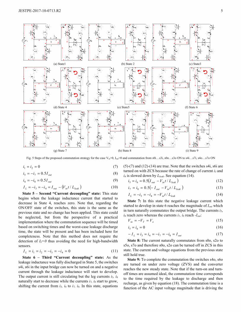
voltage are both positive and both the input and output bridges are commutated, as shown in Fig. 5. The generalisation to all the possible commutation states can be obtained by rearranging the order of the different commutation steps, as discussed in Section V. The analysis assumes that the input voltage and output current remain effectively constant during the commutation interval, given that the commutation time is a negligible fraction of the input and output fundamental periods.
A. Commutation Strategy for Vin>0, Iout>0: from s0i…s3i, s0o…s3o ON to s4i…s7i, s4o…s7o ON
State 1 – Initial state: The converter is in steady state with a total of 8 switches i.e. 4 switches of input bridge s0i, s1i, s2i, s3i and 4 switches of output bridge s0o, s1o, s2o, s3o in the on state. In this initial state:
oTin VVV == (2)
Lout IIiiii ===== 6521 (3)
08743 ==== iiii (4)
State 2: With Vin>0 and Iout>0, the non-conducting switches of both bridges i.e. s1i, s3i and s1o, s3o can be turned off with ZCS, equations (2)-(4) remain true.
State3: The switches s5i, s7i and s5o, s7o can conduct the current in the direction of Iout and therefore can be turned on safely (i.e. without short circuiting Vin) with ZCS and equations (2)-(4) still hold true. The current through s5i, s7i and s5o, s7o remains zero because the antiparallel diodes of s4i, s6i and s4o, s6o are all reverse biased.
State 4 – First “Current decoupling” state: Since the switches s5i, s7i and s5o, s7o are now in the on state, they can provide a path for Iout and the switches s0i, s1i in the input bridge can be turned off safely. Note that the switches s0i, s1i will have hard turn off. When the input side switches are turned off, the leakage inductance current forces the antiparallel diodes of s4i, s6i and s4o, s6o into conduction. As a result, the output current now circulates in s0o, s5o, s2o, s7o and in the antiparallel diodes of the output bridge switches (which are in the off state). This action effectively shorts the secondary of the transformer, decoupling the input bridge from the output bridge, and in turn decoupling Iout from the leakage inductance current IL. At the input side, the reversed input voltage appears across the leakage inductance, driving the current toward zero. During this state:
0=oV (5)
inT VV −= (6)
(a) state 1 (b) state 2 (c) state 3 (d) state 4 (e) state 5
Fig. 4 Standard 4-step Current Based Commutation for the ideal converter when Iout>0 and Commutation from s0…s3 ON to s4…s7 ON
s7
Iouts0IL
s1
s6 s2
s3
s5
s4
Iin
Iout
Iin
IL
s7
s0
s1
s6 s2
s3
s5
s4Iout
Iin
IL
s7
s0
s1
s6 s2
s3
s5
s4Iout
Iin
IL
s7
s0
s1
s6 s2
s3
s5
s4Iout
Iin
IL
s7
s0
s1
s6 s2
s3
s5
s4
JESTPE-2017-10-0713.R2
5
021 == ii (7)
outIii 5.075 =−= (8)
outIii 5.086 =−= (9)
( )leakinoutL LtVIiiI /43 −=−=−= (10)
State 5 – Second “Current decoupling” state: This state begins when the leakage inductance current that started to decrease in State 4, reaches zero. Note that, regarding the ON/OFF state of the switches, this state is the same as the previous state and no change has been applied. This state could be neglected, but from the perspective of a practical implementation where the commutation sequence will be timed based on switching times and the worst-case leakage discharge time, the state will be present and has been included here for completeness. Note that this method does not require the detection of IL=0 thus avoiding the need for high-bandwidth sensors.
04321 =−=−=== iiiiI L (11)
State 6 – Third “Current decoupling” state: As the leakage inductance was fully discharged in State 5, the switches s4i, s6i in the input bridge can now be turned on and a negative current through the leakage inductance will start to develop. The output current is still circulating but the leg currents i5, i6 naturally start to decrease while the currents i7, i8 start to grow, shifting the current from i5, i6 to i7, i8. In this state, equations
(5)-(7) and (12)-(14) are true. Note that the switches s4i, s6i are turned on with ZCS because the rate of change of current i3 and i4 is slowed down by Lleak. See equation (14).
( )leakinout LtVIii /5.065 −== (12)
( )leakinout LtVIii /5.087 −−== (13)
leakinL LtViiI /43 −=−=−= (14)
State 7: In this state the negative leakage current which started to develop in state 6 reaches the magnitude of Iout which in turn naturally commutates the output bridge. The currents i5, i6 reach zero whereas the currents i7, i8 reach -Iout:
oTin VVV =−= (15)
065 == ii (16)
outL IiiiiI =−=−===− 8743 (17)
State 8: The current naturally commutates from s0o, s2o to s5o, s7o and therefore s0o, s2o can be turned off in ZCS in this state. The current and voltage equations from the previous state still hold true.
State 9: To complete the commutation the switches s4o, s6o are turned on under zero voltage (ZVS) and the converter reaches the new steady state. Note that if the turn-on and turn-off times are assumed ideal, the commutation time corresponds to the time required by the leakage to discharge and then recharge, as given by equation (18). The commutation time is a function of the AC input voltage magnitude that is driving the
(a) State1 (b) State 2 (c) State3
(d) State 4 (e) State5 (f) State 6
(g) State 7 (h) State 8 (i) State 9
Fig. 5 Steps of the proposed commutation strategy for the case Vin>0, Iout>0 and commutation from s0i…s3i, s0o…s3o ON to s4i…s7i, s4o…s7o ON

JESTPE-2017-10-0713.R2
6
current reversal. Therefore, for a desired maximum commutation time and load profile, a minimum input voltage exists below which the commutation is not possible. In such a condition, the commutation is not immediately performed, resulting in a small zero-crossing output voltage distortion.
MIN
in
MAXout
leakcommV
ILT 2> (18)
In practical applications, the commutation time must be set for the worst-case value based on the possible instantaneous values of input voltage and output current, including the impact of switching times in each of the stages. If this condition is respected, the leakage current reversal occurs without triggering the protection clamps and therefore without generating additional loss.
It is important to note, by following the above commutation states 1-9 for the example shown in in Fig. 5, that the output bridge is completely soft-switched whereas the input bridge has only one hard-switching action per commutation sequence. In state 2, all the switching actions are soft as s1i, s3i, s1o, s3o are turned off with zero current. In state 3, all the commutations are soft because s5i, s7i, s5o, s7o are turned on with zero current. In state 4, the switching actions are hard as the input side bridge switches s0i, s2i are turned off with non-zero current. Note that state 5 is same as state 4 with respect to the state of the switches. In state 6, the commutations are soft as the input side bridge switches s4i, s6i are turned on with nearly zero current because the rate change of current is limited by the leakage inductance Lleak. State 7 is same as state 6. In state 8, all the switching actions are soft as s0o, s2o are turned off with zero current and finally in state 9, the switches s4o, s6o are turned on with zero current. Therefore, during the whole commutation process, only the input side bridge switches s0i, s2i i.e. only two switches undergo hard-switching commutation while the output side bridge achieves complete soft-switching.
V. IDEAL COMMUTATION WAVEFORMS
For the conditions discussed in the previous two sections in Fig. 4 and Fig. 5, the ideal waveforms of both commutation methods have been obtained through simulation in Plecs and are reported in Fig. 6. The leakage inductance is assumed to be Lleak=3.2µH and the commutation process starts at the instant when Vin=50V, Iout=7A. In the 4-step commutation method in Fig. 6(a), the output bridge is commutating first and the transition from state 3 to state 4 triggers the protection clamp. As a result, the output voltage Vo stays at minus the clamp voltage until IL is reversed driven by the voltage VT+Vo, causing power dissipation in the clamp. On the other hand, in the proposed commutation method, shown in Fig. 6(b), IL is reversed without triggering the clamp, thanks to the proposed current decoupling phase.
The simulation results in Fig. 7 show that the proposed commutation strategy for the single-phase isolated AC/AC converter is applicable regardless of the direction of the power flow. In Fig .7(a), the power flows from the voltage source to the current source and the commutation sequence in the zoom
in Fig. 7(b) is the same as the one discussed in Section IV. The power flow is reversed in Fig. 7(c), the commutation concept is still applicable but with a commutation path which is different from that of Fig. 7(b). For brevity, only the case of Fig. 7(a) is discussed in detail and validated experimentally in the paper. For completeness, all the commutation paths have been summarised in a Finite State Machine (FSM) later in Section VII.
VI. COMMUTATION PATHS
The commutation strategy has been discussed so far for the case where the required change of state is from VT>0, VO>0 to VT<0, Vo>0 when Vin>0, Iout>0. The same strategy can be extended to all the possible changes of the switch states of the converter, by rearranging the sequencing of the commutation procedure. The possible steady states of the converter are shown in Table I, coded with an alphabetic sequence, where the first letter represents the state matrix for the input bridge switches and the second letter the state matrix for the output bridge. The generic bridge state matrix is defined as:
],[ 3276
5410oiy
ssss
ssssX
yyyy
yyyy ∈
= (19)
Fig. 6 Ideal commutation waveforms when Vin>0, Iout>0. (a) With 4-step commutation (b) With proposed Leakage-Inductance-Tolerant
commutation method.
Clamp ON31 894542 321 7
0 0
1) 50V/div 2) 7A/div 3) 50V/div 1µs/div
(a) (b)
6
0
0 0
0
VT VT
1)
2)
3)
IL IL
Vo Vo
T
leak
V
L
( )T o
leak
V V
L
+
(a) (b) (c) (d) Fig. 7 Simulation results (a) Power flow direction from voltage source to current source (b) Zoom of (a) - single commutation (c) Power flow direction from current source to voltage source (d) Zoom of (c) - single
commutation.
3µs/div
3)250V/div 4)30A/div1)250V/div 2)30A/div
10ms/div
0
0
0
VT
Iout
IT
Vin 0
3µs/div3)250V/div 4)30A/div1)250V/div 2)30A/div
10ms/div
0
0
VT
Iout
IT
Vin

JESTPE-2017-10-0713.R2
7
Where the switch numbering 0…7 refers to the individual switches in the bidirectional bridges as shown in Fig. 5. The definition of the state matrices is given in (20). As already seen in the commutation example, only a few states (A,D,J) are used in steady state, while the remaining ones (B,C,E,F,G,H,I,K,L,M,N) are needed only during the commutation process.
11 00 10 00 01 00 00 11 00 10, , , , ,
00 11 00 10 00 01 11 00 10 00
00 01 11 01 10 01 00 00 00 00, , , , ,
01 00 01 11 01 10 01 10 11 11
01 10 01 11,
10 01 11 01
A B C D E
F G H I J
K L
= = = = = = = = = = = =
01 01 10 10, ,
01 01 10 10M N
= =
(20)
TABLE I: AVAILABLE STEADY STATES OF THE CONVERTER
Fig. 8 shows a simplified commutation path diagram to move
between the steady states listed in Table I for the case when Vin>0, Iout>0. The commutation paths are represented by arrows, temporary commutation states by small circles and steady states by large grey circles. For instance, to move from steady state ‘AA’ to ‘DA’, the converter will go through two commutation states i.e. ‘GA’ and ‘FA’. With a similar approach and using the same definitions of state matrices, three additional graphs can be derived, corresponding to the commutation paths for (Vin>0, Iout<0), (Vin<0, Iout>0) and (Vin<0, Iout<0).
VII. EXPERIMENTAL RESULTS
A proof-of-concept prototype of the converter has been built and tested to validate the proposed leakage-inductance-tolerant commutation concept. The architecture of the experimental converter is shown in Fig. 9. The experimental rig shown in Fig. 10 has been designed using SEMIKRON SKM150GM12T4G IGBT power modules, each containing two series connected IGBTs with common emitters to implement the four quadrant switches required by the fully bi-directional H bridges. The two H-bridges have been designed for a VA rating of 45kVA (600V,
75A) to develop a flexible and scalable test rig to validate different isolated AC/AC topologies. However, the experimental setup used for the results reported in this paper has total power limited to 3kW by the design of the MF transformer. This choice has been made to simplify the proof-of-concept validation and also to be able to compare the proposed leakage-inductance-tolerant commutation strategy with a 4-step method without excessive power dissipation in the clamp circuits, caused by the reversal of the current through the leakage inductance.
The parameters of the MF transformer, based on C-cores and operating at 10kHz, are reported in Table II. As shown in Fig. 9, the converter feeds a simple RL circuit, with filter inductor and load resistor reported in Table III. A filter capacitor CF, also listed in Table III, filters the input current harmonics and provides voltage source characteristics for the input side bridge. A custom DSP/FPGA control platform based on the TMS320C6713DSK optically transmits gate signals and receives voltage and current sign information, required by the proposed commutation strategy.
State Code VT sign Vo sign AA + + AD + - DD - + DA - - AJ + 0 DJ - 0
Fig. 8 Commutation paths when Vin>0, Iout>0
AA
AJ
DD
DJDA AD
GA
FA
FA
HA
BA
CD
KD
ED
FB
FH
DH
DF
LD
CD
CF
CH
AH
AB
CI
CJ
FI
FJ
DB
LF
CF
AF
GB
FB
AI
AHDH
DI
(a)
(b)
Fig. 9 Experimental setup diagram (a) Overall system (b) Output clamp circuit configuration
Ccl
am
p
R
D1o
D2o
D3o
D4o
D1i
D2i
D3i
D4i
Iclamp_2oIclamp_2i
Iclamp2
Vclamp2+
-
Fig. 10 Photo of the experimental prototype of the single-phase
isolated AC/AC converter built for proof-of-concept validation of the proposed leakage-inductance-tolerant commutation strategy.

JESTPE-2017-10-0713.R2
8
TABLE II: TRANSFORMER PARAMETERS
Parameter Value
Core Material and shape 2xAMCC16B C-cores
Amorphous alloy 2605SA1 Leakage Inductance Lleak 3.2µH
Magnetisation Inductance Lm 1.5mH
Operating Frequency fsw 10kHz
Number of Turns N 16
Turns Ratio N1/N2 1:1
RMS current at fsw 15A
RMS voltage at fsw 200V
Power rating 3kVA
As discussed in Section V and depicted in Fig. 8 for Vin>0,
Iout>0, different commutation paths exist and for each of them a leakage-inductance-tolerant commutation strategy based on the current decoupling concept can be developed. For the sake of brevity, experimental results are shown in a simplified open-loop operating mode where the input bridge modulates the low frequency input voltage (50Hz) at 10kHz with 50% duty cycle. After the MF transformer, the voltage waveform is demodulated by the output bridge to reconstruct – in the assumption of ideal and instantaneous commutation - the same input voltage waveform, thus obtaining a simple 1:1, 50Hz to 50Hz, isolated AC/AC converter. As a result, the power
converter always moves between the two steady states ‘AA’ and ‘DD’. Defining s(t) as a square wave function at 10kHz and 50% duty cycle:
( )( ) ( )
21 0,1,2..( )2 11
sw sw sw
sw sw sw
for nT t nT T state AA ns tfor nT T t n T state DD
< < + → == + < < + →− (21)
In the case of ideal commutation, the transformer voltage and the output voltage in the simple operating mode under study can be written as:
( )
( )T in
o T in
V s t V
V s t V V
= = =
(22)
TABLE III: PROTOTYPE PARAMETERS
Parameter Symbol Value 50Hz Input Voltage Amplitude Vin 100V RMS Load Resistance R 7.8 Ω Load Inductance L 18mH Input Filter Capacitance CF 30µF Clamp capacitor Cclamp 300µF Clamp resistor R 22kΩ
In the following subsections, the proposed leakage-inductance-tolerant commutation process for the simplified operating mode discussed above is validated experimentally and compared against a standard 4-step commutation strategy. All the experimental tests have been conducted with the converter in Fig. 10 operating with the parameters reported in Table III.
(a) (b)
(c) (d) Fig. 11 Experimental results with standard 4-step commutation method. (a) Voltages and currents at the converter terminals. (b) Transformer voltage and current and clamp voltages. (c) Activation of the clamp during commutation. (d) Expanded view of the region highlighted in (c), showing current through the output clamp capacitor due to the leakage inductance effect on the transition from state 3 to state 4.
JESTPE-2017-10-0713.R2
9
A. Standard 4-Step Commutation Method
The 4-step commutation method is first applied to both the input and the output bridges and the observed results are presented in Fig. 11. Fig. 11(a) shows the recorded waveforms of input voltage Vin, output voltage VO and output current Io. Fig. 11(b) shows the transformer voltage VT, transformer or leakage current IL, clamp circuit voltages Vclamp1 (input clamp) and Vclamp2 (output clamp).
To highlight the limitation of the standard 4-step current based commutation, the switching sequence of the output bridge, shown in Fig. 4, must be considered. The transition from state 3 to state 4, will cause an overvoltage that will trigger the output protection clamp and the leakage current IT together with the output current Iout will flow into the output side clamp circuit as seen observing Iclamp_2o in Fig. 11(d). This will cause the output voltage to be clamped i.e. Vo=Vclamp2. Since Vclamp2 > Vin and Vo=Vclamp2 the leakage current IL starts decreasing until IL=-Iout as shown in Fig. 11(d). Iclamp_2o and Vclamp2 are defined in Fig. 9(b).
From the discussion above, it is clear that the leakage energy is absorbed by the clamp circuit and each commutation will cause power loss as the energy gets dissipated in the clamp resistor. Therefore, it is not recommended to operate the converter with standard 4-step commutation at high power in the presence of non-negligible leakage-inductance in the transformer.
B. Proposed Leakage-Inductance-Tolerant Commutation Strategy
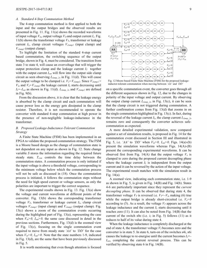
A Finite State Machine (FSM) has been implemented in an FPGA to validate the proposed commutation strategy. The FSM is a Moore based design as the change of commutation state is not dependent on any input as shown in Fig. 12. State change variable S stores the information regarding the required future steady state. Tcom controls the time delay between the commutation states. A commutation process is only initiated if the input voltage is above a threshold voltage, corresponding to the minimum voltage below which the commutation process will not be safe as discussed in (18). Once the commutation process is initiated, it follows the commutation steps without the need for high speed current or voltage sensors, as only the polarities are important to trigger the correct sequence.
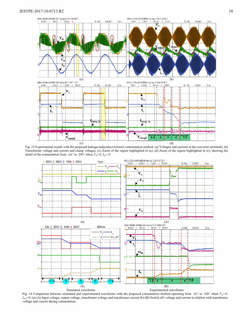
The experimental results shown in Fig. 13. Fig. 13(a) show the voltage and current waveforms at different points of the converter. Fig. 13(b) shows the corresponding transformer voltage VT, transformer or leakage current IL, clamp circuit voltages Vclamp1 (input clamp) and Vclamp2 (output clamp). Fig. 13(c) shows a zoom of the commutation events occurring during the highlighted part of Fig. 13(a), representing the case when Vin>0, Iout>0, the same case discussed in detail in the previous sections. Furthermore, Fig. 13(d) is the zoomed view of Fig. 13(c), focusing on the single commutation event required to move from steady state ‘AA’ to ‘DD’ for the case when Vin>0, Iout>0. Note that the state numbers 1-9, indicated in Fig. 13(d), are the same that have been previously discussed in Fig. 5.
It is worth mentioning that even though attention is focused
on a specific commutation event, the converter goes through all the different sequences shown in Fig. 12, due to the changes in polarity of the input voltage and output current. By observing the output clamp current Iclamp_2o in Fig. 13(c), it can be seen that the clamp circuit is not triggered during commutation. A further confirmation comes from Fig. 13(d) that zooms in on the single commutation highlighted in Fig. 13(c). In fact, during the reversal of the leakage current IL, the clamp current Iclamp_2o remains zero and consequently the converter achieves safe-commutation as expected.
A more detailed experimental validation, now compared against a set of simulation results, is proposed in Fig. 14 for the commutation event discussed in Section III and illustrated in Fig. 5, i.e. ‘AA’ to ‘DD’ when Vin>0, Iout>0. Figs. 14(a)-(b) present the simulation waveforms whereas Figs. 14(A)-(B) present the corresponding experimental waveforms. It can be observed first from Fig. 14(A) that the output voltage Vo is clamped to zero during the proposed current decoupling phase where the leakage current IL is independent from the output current and it can be reversed by the action of the input voltage. The experimental result matches with the simulation result in Fig. 14(a).
A zoomed view, indicating each commutation state, i.e. 1-9 as shown in Fig. 5, is given in Fig. 14(B) and Fig. 14(b). States 4-6 are particularly important since they represent the current decoupling phase. It can be observed that during state 4, the transformer voltage VT is reversed i.e. VT=-Vin making (6) true while the output bridge is already short-circuited i.e. Vo=0 according to (5). As a result, the voltage VT appears across the leakage inductance and the current IL starts decreasing until it reaches zero (11). It can also be noted from Fig. 14(B) that the current of the switch s0o (i.e. i5 in Fig. 5) follows (11) as it reduces to half of its value during state 4.
When the leakage inductance is completely discharged at the end of state 4, the transformer voltage VT becomes zero and the converter is in state 5. In state 6, turn-on of the switches s4i, s6i causes the leakage to re-energise until the current becomes IL=-Iout, completing the current reversal process. This can be verified by observing state 6 in Fig. 14(B).
Fig. 12 Moore based Finite State Machine (FSM) for the proposed leakage-inductor-tolerant commutation when moving between ‘AA’ and ‘DD’
DD
S=DD or|Vin|<VTH
AA
S=AA or
|Vin|<VTH
Vin>0,Iout>0
S=DD,|Vin|>VTH
Vin>0,Iout<0
BB HH FH DH DF
CC MK FK HK FE
BB NH EH KH EFVin<0,Iout>0
CC KK EK DK DEVin<0,Iout<0
AC AK BK HK FE
BB HH BH NH EF
CC KK CK MK FE
AB AH CH KH EF
S=AA,|Vin|>VTH
Vin>0,Iout>0
Vin>0,Iout<0
Vin<0,Iout>0
Vin<0,Iout<0
Vin,Iout,Tcom,S Vin,Iout,Tcom,S
JESTPE-2017-10-0713.R2
10
12
(a) (b)
(c) (d)
Fig. 13 Experimental results with the proposed leakage-inductance-tolerant commutation method. (a) Voltages and currents at the converter terminals; (b) Transformer voltage and current and clamp voltages; (c) Zoom of the region highlighted in (a); (d) Zoom of the region highlighted in (c), showing the detail of the commutation from ‘AA’ to ‘DD’ when Vin>0, Iout>0
(a) (A)
(b) (B)
Simulated waveforms Experimented waveforms Fig. 14 Comparison between simulated and experimented waveforms with the proposed commutation method operating from ‘AA’ to ‘DD’ when Vin>0, Iout>0: (a)-(A) Input voltage, output voltage, transformer voltage and transformer current (b)-(B) Switch s01 voltage and current in relation with transformer voltage and current during commutation.
-100
0
100
200
VIN
VO
IL
-VT
0
0
0
0
1. 50V/ 2. 50V/ 3. 10A/ 4. 50V/ 1µs/
200
100
0
100
200
VT
IL
-I5
Vs_01
0
0
0
0
1. 5A/ 2. 50V/ 3. 10A/ 4. 50V/ 500ns/
51-3 4 6 7-9
JESTPE-2017-10-0713.R2
11
Note that the slope of the leakage current IL, in state 4 and state 6, is dependent on the ratio Vin/Lleak. At the end of state 6, the current i5 which was carried by the switches s0o, s2o is naturally commutated to switches s5o, s7o. The switches s0o, s2o can therefore be turned OFF with ZCS. This can also be observed in Fig. 14(B) since the current of the switch s0o is approximately zero at the beginning of the turn OFF commutation (end of state 6 interval), in line with the explanation in Section III. Similarly, the ZCS turn-on of the switches s5o, s7o can also be validated by observing the current i7 and the voltage Vs45, not included for brevity.
A final observation is that the commutation results shown in Fig. 13(d) and Fig. 14 focus on the transition from ‘AA’ to ‘DD’ when Vin>0,Iout>0, for consistency with the discussion presented in section III. However, when the input voltage is sinusoidal the converter commutates between all the possible paths shown in Fig. 12. Among those, the transition from steady state ‘AA’ to ‘DD’ when Vin>0,Iout<0, takes the converter through the commutation states ‘CC’, ‘MK’, ‘FK’, ‘HK’, ‘FE’. During the intermediate state ‘HK’, the output voltage is VO=-Vin and this justifies the behaviour of the output voltage highlighted with red circles in Fig. 13(a).
VIII. SEMICONDUCTOR LOSSES AND STRESSES
In this section, the proposed method and the standard 4-step commutation method are compared in terms of the impact of semiconductor power losses and stresses, considering the operating conditions of the experimental setup. Simulation and experimental loss measurements are shown, confirming the loss reduction achieved with the proposed method. It is important to note that only semiconductor and clamp losses are included in the analysis. In addition, the experimental prototype has been designed to be a flexible proof-of-concept demonstrator, not optimised for efficiency. Therefore, the loss values reported in this section are not representative of the technology but can only be used for a relative comparison between the two commutation strategies.
A. V-I stresses
The current stress in the 4-step and in the modified commutation strategy are the same, since the currents only depend on the operating points of the converter. However, the voltage stress across the bi-directional switches is different in the two methods. In the 4-step commutation, the output protection clamp in Fig. 9(b) triggers every time the current through the transformer is flipped. In this case the voltage stress of the output bridge switches is the clamp voltage, approximately equal to the peak of the input AC voltage. The voltage stress across the input bridge switches is the instantaneous AC grid voltage. Conversely, in the proposed commutation method, the energy stored in the transformer leakage is recovered and the output clamp does not trigger in normal operation. As a result, the voltage stress of the input and output switches is always limited to the instantaneous AC grid voltage.
B. Leakage inductance related losses in 4-step commutation
As discussed above, in the 4-step method the output clamp triggers every time the transformer current is flipped, leading to two activations of the clamp per switching period. As shown in Fig. 11 (d), the clamp current Iclamp_2o can be approximated as a triangular wave with amplitude 2Iout that decreases with a slope
of ( )2( ) /in clamp leakV t V L− . In the assumption that Vclamp2 is
constant, the clamp losses caused by the leakage inductance, averaged over a switching period, can be written as:
( )( )2
_
_
2
4 sin( )
sin( )1
out pk o leak sw
in pk o
clamp
I t L fP t
V t
V
ω θ
ω
−=
−
(23)
C. Switching Losses
The switching losses for the operating conditions of the experimental prototype considered with the 4-step method can be discussed referring to Fig. 4. Each bridge undergoes a total of 8 switch transitions, 2 of which are hard, every time the state changes from ‘AA’ to ‘DD’. With the proposed method, the switch transitions when moving from ‘AA’ to ‘DD’ when Vin>0,Iout>0, have been discussed in in Section IV and are a total of 16 out of which 2 are hard. A comparison between the two methods, for the operating mode under study, is reported in Table IV.
TABLE IV: COMPARISON OF SWITCH TRANSITIONS IN 4-STEP AND LEAKAGE-INDUCTANCE-TOLERANT COMMUTATION METHODS
In addition, in the proposed commutation method di/dt at turn-off is limited by Lleak, reducing the reverse recovery loss.
Commutation Method
No. of switch transitions Input bridge
No. of switch transitions Output bridge
4-step Total 8 Total 8
Soft Hard Soft Hard 6 2 6 2
Leakage-Inductance-Tolerant
Total 8 Total 8 Soft Hard Soft Hard
6 2 8 0
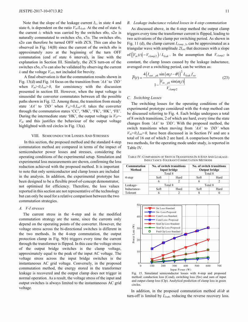
Fig. 15. Simulated semiconductor losses with 4-step and proposed method: conduction loss (Cond), switching loss (Sw) and sum of input and output clamp loss (Clp). Analytical prediction of clamp loss in green circles.
0 100 200 300 400 500 600 7000
10
20
30
40
50
Input Power (W)
Pow
er L
oss
(W)
Sw Loss-Standard
Sw- Loss-Proposed
Cond Loss-Standard
Cond Loss- Proposed
Sim Clp Loss-Standard
Sim Clp Loss-Proposed
Pred Clp Loss-Standard
JESTPE-2017-10-0713.R2
12
As a result, the proposed method is expected to considerably reduce switching losses when compared with the 4-step method, as shown in the Plecs simulation in Fig. 15. For simplicity, results are taken varying the power by varying the input voltage magnitude, maintaining the same RL load at the output. The figure also confirms that conduction losses do not change with the commutation method. Moreover, the leakage inductance related losses predicted by averaging (23) over half of the fundamental period are validated against the corresponding simulated losses.
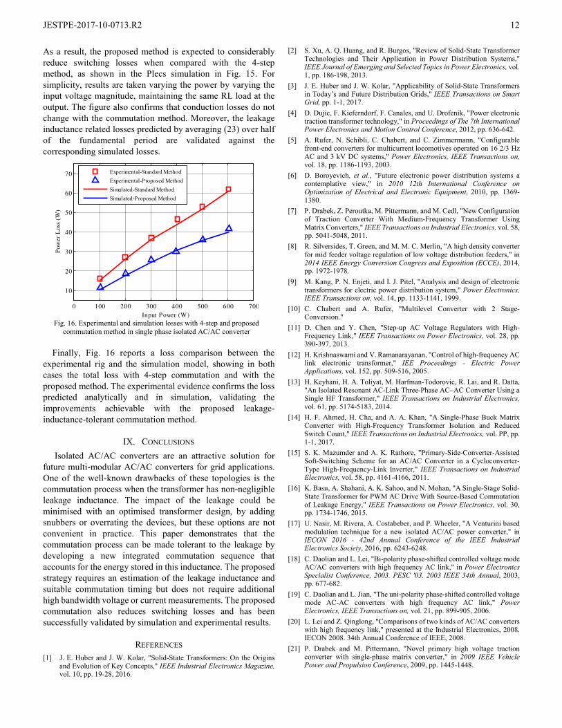
Finally, Fig. 16 reports a loss comparison between the experimental rig and the simulation model, showing in both cases the total loss with 4-step commutation and with the proposed method. The experimental evidence confirms the loss predicted analytically and in simulation, validating the improvements achievable with the proposed leakage-inductance-tolerant commutation method.
IX. CONCLUSIONS
Isolated AC/AC converters are an attractive solution for future multi-modular AC/AC converters for grid applications. One of the well-known drawbacks of these topologies is the commutation process when the transformer has non-negligible leakage inductance. The impact of the leakage could be minimised with an optimised transformer design, by adding snubbers or overrating the devices, but these options are not convenient in practice. This paper demonstrates that the commutation process can be made tolerant to the leakage by developing a new integrated commutation sequence that accounts for the energy stored in this inductance. The proposed strategy requires an estimation of the leakage inductance and suitable commutation timing but does not require additional high bandwidth voltage or current measurements. The proposed commutation also reduces switching losses and has been successfully validated by simulation and experimental results.
REFERENCES [1] J. E. Huber and J. W. Kolar, "Solid-State Transformers: On the Origins
and Evolution of Key Concepts," IEEE Industrial Electronics Magazine, vol. 10, pp. 19-28, 2016.
[2] S. Xu, A. Q. Huang, and R. Burgos, "Review of Solid-State Transformer Technologies and Their Application in Power Distribution Systems," IEEE Journal of Emerging and Selected Topics in Power Electronics, vol. 1, pp. 186-198, 2013.
[3] J. E. Huber and J. W. Kolar, "Applicability of Solid-State Transformers in Today’s and Future Distribution Grids," IEEE Transactions on Smart Grid, pp. 1-1, 2017.
[4] D. Dujic, F. Kieferndorf, F. Canales, and U. Drofenik, "Power electronic traction transformer technology," in Proceedings of The 7th International Power Electronics and Motion Control Conference, 2012, pp. 636-642.
[5] A. Rufer, N. Schibli, C. Chabert, and C. Zimmermann, "Configurable front-end converters for multicurrent locomotives operated on 16 2/3 Hz AC and 3 kV DC systems," Power Electronics, IEEE Transactions on, vol. 18, pp. 1186-1193, 2003.
[6] D. Boroyevich, et al., "Future electronic power distribution systems a contemplative view," in 2010 12th International Conference on Optimization of Electrical and Electronic Equipment, 2010, pp. 1369-1380.
[7] P. Drabek, Z. Peroutka, M. Pittermann, and M. Cedl, "New Configuration of Traction Converter With Medium-Frequency Transformer Using Matrix Converters," IEEE Transactions on Industrial Electronics, vol. 58, pp. 5041-5048, 2011.
[8] R. Silversides, T. Green, and M. M. C. Merlin, "A high density converter for mid feeder voltage regulation of low voltage distribution feeders," in 2014 IEEE Energy Conversion Congress and Exposition (ECCE), 2014, pp. 1972-1978.
[9] M. Kang, P. N. Enjeti, and I. J. Pitel, "Analysis and design of electronic transformers for electric power distribution system," Power Electronics, IEEE Transactions on, vol. 14, pp. 1133-1141, 1999.
[10] C. Chabert and A. Rufer, "Multilevel Converter with 2 Stage-Conversion."
[11] D. Chen and Y. Chen, "Step-up AC Voltage Regulators with High-Frequency Link," IEEE Transactions on Power Electronics, vol. 28, pp. 390-397, 2013.
[12] H. Krishnaswami and V. Ramanarayanan, "Control of high-frequency AC link electronic transformer," IEE Proceedings - Electric Power Applications, vol. 152, pp. 509-516, 2005.
[13] H. Keyhani, H. A. Toliyat, M. Harfman-Todorovic, R. Lai, and R. Datta, "An Isolated Resonant AC-Link Three-Phase AC–AC Converter Using a Single HF Transformer," IEEE Transactions on Industrial Electronics, vol. 61, pp. 5174-5183, 2014.
[14] H. F. Ahmed, H. Cha, and A. A. Khan, "A Single-Phase Buck Matrix Converter with High-Frequency Transformer Isolation and Reduced Switch Count," IEEE Transactions on Industrial Electronics, vol. PP, pp. 1-1, 2017.
[15] S. K. Mazumder and A. K. Rathore, "Primary-Side-Converter-Assisted Soft-Switching Scheme for an AC/AC Converter in a Cycloconverter-Type High-Frequency-Link Inverter," IEEE Transactions on Industrial Electronics, vol. 58, pp. 4161-4166, 2011.
[16] K. Basu, A. Shahani, A. K. Sahoo, and N. Mohan, "A Single-Stage Solid-State Transformer for PWM AC Drive With Source-Based Commutation of Leakage Energy," IEEE Transactions on Power Electronics, vol. 30, pp. 1734-1746, 2015.
[17] U. Nasir, M. Rivera, A. Costabeber, and P. Wheeler, "A Venturini based modulation technique for a new isolated AC/AC power converter," in IECON 2016 - 42nd Annual Conference of the IEEE Industrial Electronics Society, 2016, pp. 6243-6248.
[18] C. Daolian and L. Lei, "Bi-polarity phase-shifted controlled voltage mode AC/AC converters with high frequency AC link," in Power Electronics Specialist Conference, 2003. PESC '03. 2003 IEEE 34th Annual, 2003, pp. 677-682.
[19] C. Daolian and L. Jian, "The uni-polarity phase-shifted controlled voltage mode AC-AC converters with high frequency AC link," Power Electronics, IEEE Transactions on, vol. 21, pp. 899-905, 2006.
[20] L. Lei and Z. Qinglong, "Comparisons of two kinds of AC/AC converters with high frequency link," presented at the Industrial Electronics, 2008. IECON 2008. 34th Annual Conference of IEEE, 2008.
[21] P. Drabek and M. Pittermann, "Novel primary high voltage traction converter with single-phase matrix converter," in 2009 IEEE Vehicle Power and Propulsion Conference, 2009, pp. 1445-1448.
Fig. 16. Experimental and simulation losses with 4-step and proposed
commutation method in single phase isolated AC/AC converter
0 100 200 300 400 500 600 700
10
20
30
40
50
60
70
Input Power (W)
Pow
er L
oss
(W)
Experimental-Standard Method
Experimental-Proposed Method
Simulated-Standard Method
Simulated-Proposed Method

JESTPE-2017-10-0713.R2
13
[22] C. Daolian, "Novel Current-Mode AC/AC Converters With High-Frequency AC Link," Industrial Electronics, IEEE Transactions on, vol. 55, pp. 30-37, 2008.
[23] N. Burany, "Safe control of four-quadrant switches," in Industry Applications Society Annual Meeting, 1989., Conference Record of the 1989 IEEE, 1989, pp. 1190-1194 vol.1.
[24] S. Norrga, "Experimental Study of a Soft-Switched Isolated Bidirectional AC/DC Converter Without Auxiliary Circuit," IEEE Transactions on Power Electronics, vol. 21, pp. 1580-1587, 2006.
Usman Nasir received his B.Sc. degree in Electrical Engineering from the National University of Sciences and Technology (NUST), Islamabad, Pakistan in 2013 and he received his M.Sc. degree in Electric Power System & Its Automation from North China Electric Power University, Beijing, China in 2015. He is currently working towards his PhD degree in Electrical Engineering and is associated with PEMC group at the University of Nottingham, UK. He is a recipient of ‘Dean of Engineering Scholarship for International Research Excellence’
for his PhD studies. His research interests include new matrix converter based topologies, novel commutation algorithms, new modulation techniques and Model Predictive Control (MPC) for power electronic converters. He received best paper award in IEEE SPEC 2017, Chile.
Alessandro Costabeber received the MSc degree with honours in Electronic Engineering from the University of Padova, Italy, in 2008 and the Ph.D. in Information Engineering from the same university in 2012, on energy efficient architectures and control for future residential microgrids. In 2014 he joined the PEMC group at the University of Nottingham, UK as Lecturer in Power Electronics. His current research interests include modular multilevel converters for HVDC, high power density converters, control and stability analysis of AC and
DC microgrids. Dr. Costabeber received the IEEE Joseph John Suozzi INTELEC Fellowship Award in Power Electronics in 2011.
Marco Rivera received his B.Sc. in Electronics Engineering and M.Sc. in Electrical Engineering from the Universidad de Concepción, Chile in 2007 and 2008, respectively. He earned his PhD degree at the Department of Electronics Engineering, Universidad Técnica Federico Santa María, in Valparaíso, Chile, in 2011 with a scholarship from the Chilean Research Fund CONICYT. During 2011 and 2012, he was working as a postdoc researcher and part-time professor at the Department of Electronics Engineering, Universidad Técnica Federico Santa
María, in Valparaíso, Chile. His research interests include matrix converters, predictive and digital controls for high-power drives, four-leg converters, and the development of high performance control platforms based on Field-Programmable Gate Arrays. Currently, he is a professor in the Department of Electrical Engineering at Universidad de Talca, Curicó, Chile. In 2013 Prof. Rivera was awarded with the Premio Tesis de Doctorado Academia Chilena de Ciencias 2012, which was awarded to the best PhD Thesis developed in 2011 for national and foreign students in any exact or natural sciences program that is a member of the Academia Chilena de Ciencias, Chile. In 2015 he was awarded as the Oustanding Engineer of 2015, award given by the Chilean Association of Electrical and Electronics Industry and the IEEE-Chile.
Pat Wheeler received his BEng [Hons] degree in 1990 from the University of Bristol, UK. He received his PhD degree in Electrical Engineering for his work on Matrix Converters from the University of Bristol, UK in 1994. In 1993 he moved to the University of Nottingham and worked as a research assistant in the Department of Electrical and Electronic Engineering. In 1996 he became a Lecturer in the Power Electronics, Machines and Control Group at the University of Nottingham, UK. Since January 2008 he has been a Full Professor in the same research group. He is
currently Head of the Department of Electrical and Electronic Engineering at the University of Nottingham. He is an IEEE PELs ‘Member at Large’ and an IEEE PELs Distinguished Lecturer. He has published 400 academic publications in leading international conferences and journals.
Jon Clare was born in Bristol, U.K., in 1957. He received the B.Eng. and Ph.D. degrees in electrical engineering from the University of Bristol, Bristol, U.K., in 1979 and 1990, respectively. From 1984 to 1990, he was a Research Assistant and a Lecturer at the University of Bristol, where he was involved in teaching and research of power electronic systems. Since 1990, he has been with the Power Electronics, Machines and Control Research Group, University of Nottingham, Nottingham, U.K., where he is currently a Professor of power electronics and Head of Research
Group. His research interests include power electronic converter topologies, modulation and control strategies, and power conversion systems.