a-sige:h materials and devices deposited by hot wire cvd ... · pdf fileusing a tantalum...
TRANSCRIPT
National Renewable Energy Laboratory 1617 Cole Boulevard, Golden, Colorado 80401-3393 303-275-3000 • www.nrel.gov
Operated for the U.S. Department of Energy Office of Energy Efficiency and Renewable Energy by Midwest Research Institute • Battelle
Contract No. DE-AC36-99-GO10337
A.H. Mahan, Y. Xu, L.M. Gedvilas, R.C. Reedy and H.M. Branz National Renewable Energy Laboratory
D.L. Williamson Colorado School of Mines
S. Datta and J.D. Cohen University of Oregon
B. Yan United Solar Ovonics Corporation
Prepared for the 31st IEEE Photovoltaics Specialists Conference and Exhibition Lake Buena Vista, Florida January 3–7, 2005
February 2005 • NREL/CP-520-37475
a-SiGe:H Materials and Devices Deposited by Hot Wire CVD Using a Tantalum Filament Operated at Low Temperature
NOTICE
The submitted manuscript has been offered by an employee of the Midwest Research Institute (MRI), a contractor of the US Government under Contract No. DE-AC36-99GO10337. Accordingly, the US Government and MRI retain a nonexclusive royalty-free license to publish or reproduce the published form of this contribution, or allow others to do so, for US Government purposes.
This report was prepared as an account of work sponsored by an agency of the United States government. Neither the United States government nor any agency thereof, nor any of their employees, makes any warranty, express or implied, or assumes any legal liability or responsibility for the accuracy, completeness, or usefulness of any information, apparatus, product, or process disclosed, or represents that its use would not infringe privately owned rights. Reference herein to any specific commercial product, process, or service by trade name, trademark, manufacturer, or otherwise does not necessarily constitute or imply its endorsement, recommendation, or favoring by the United States government or any agency thereof. The views and opinions of authors expressed herein do not necessarily state or reflect those of the United States government or any agency thereof.
Available electronically at http://www.osti.gov/bridge
Available for a processing fee to U.S. Department of Energy and its contractors, in paper, from:
U.S. Department of Energy Office of Scientific and Technical Information P.O. Box 62 Oak Ridge, TN 37831-0062 phone: 865.576.8401 fax: 865.576.5728 email: mailto:[email protected]
Available for sale to the public, in paper, from: U.S. Department of Commerce National Technical Information Service 5285 Port Royal Road Springfield, VA 22161 phone: 800.553.6847 fax: 703.605.6900 email: [email protected] online ordering: http://www.ntis.gov/ordering.htm
Printed on paper containing at least 50% wastepaper, including 20% postconsumer waste
a-SiGe:H Materials and Devices Deposited by Hot Wire CVD Using a Tantalum Filament Operated at Low Temperature
A.H. Mahan, Y. Xu, L.M. Gedvilas, R.C. Reedy, D.L. Williamson*, S. Datta**, J.D. Cohen**, B. Yan***, and H.M. Branz NREL, 1617 Cole Blvd., Golden, CO 80401
*Colorado School of Mines, Golden, CO 80401 ** Physics Department, Univ. of Oregon, Eugene, OR 97403
***United Solar Ovonics Corporation, 1100 W. Maple Road, Troy, MI 48084
Abstract
We report the deposition of improved hydrogenated amorphous silicon germanium (a-SiGe:H) films by the Hot Wire CVD (HWCVD) technique using a tantalum filament operating at a low temperature. We gauge the material quality of the a-SiGe:H films by comparing infrared, small angle x-ray scattering (SAXS), photocapacitance and conductivity measurements to earlier results, and fabricate single junction n-i-p solar cell devices using these i-layers.
Introduction
The incorporation of high Ge content a-SiGe:H into a low bandgap solar cell commonly involves the use of bandgap profiling, where the lowest bandgap, or the highest Ge content, material is placed near the middle of the i-layer to avoid an abrupt bandgap transition at the n/i and p/i interfaces (1,2). Since in this approach the a-SiGe:H must be profiled over a wide range of Ge content, all i-layer alloy compositions, including that of a-Si:H without Ge, must be of device quality and must be deposited using similar process conditions. Previously, these conditions were not met in HWCVD, as the process conditions to deposit the a-Si:H and a-SiGe:H films were quite different. In particular, our best quality a-Si:H was typically deposited at high filament temperatures using a tungsten (W) filament (3,4), but we could only deposit our device quality a-SiGe:H using a smaller diameter W filament operating at temperatures so low that deposition reproducibility and filament lifetime were significant issues (5). This work reports on deposition of optimum quality a-SiGe:H by the HWCVD technique using a tantalum (Ta) filament also operating at low temperatures (6). We gauge the material quality by comparing infrared, small angle x-ray scattering (SAXS), and photocapacitance results to those presented elsewhere, and conclude that the structural heterogeneity of the HWCVD a-SiGe:H films can be significantly reduced compared to those deposited by PECVD by using low filament temperatures. We show that this improved structural homogeneity translates into improved electronic properties, as measured by the sl/sd conductivity ratio, and we also report preliminary results on single junction n-i-p solar cell devices using these i-layers.
Experimental
The a-SiGe:H films were grown by HWCVD using a 0.5-mm-diameter Ta filament located 5 cm from the substrate holder, in a tube reactor described elsewhere [7]. The filament
a T
temperature (Tfil) was estimated from the filament current (8), and was also calibrated using a two wavelength pyrometer under vacuum conditions (9). Table I gives representative deposition parameters for a 1.25 eV bandgap a-SiGe:H film containing 65 at.% Ge, deposited using a filament temperature of 1750°C and
sub of 200°C; it exhibited a photo-to-dark conductivity ratio of 140. To change the film bandgap, the film Ge content was varied by changing the GeH4/SiH4 gas flow ratio while keeping the total (SiH4 + GeH4) gas flow equal to the H2 flow (25 sccm). Previous work (6) has shown that film reproducibility and filament lifetime are not problems when using a Ta filament operated at low Tfil, in that more than 10-12 µm of material can be deposited reproducibly without a filament change.
SiH4 (sccm)
GeH4 (sccm)
H2 (sccm)
Pch (mT)
Rd (Å/s)
16 9 25 12.5 2.5 Table I.
Each film was deposited simultaneously on 1737F Corning glass and c-Si wafers, with evaporated coplanar (width to length ratio of 0.05) Cr contacts on the films for conductivity measurements. Optical measurements were performed on these films using an n&k 1280 Analyzer to determine the Tauc’s bandgap; this was obtained from fitting E vs. (ahn)1/2, where a is calculated by the method of interference-free determination of a from the transmission and reflection data (10). Fourier transmission infrared (FTIR) absorption spectra were obtained from transmission measurements, for films deposited simultaneously on c-Si wafers, using a Nicolet 510 system
-1operating between 400 and 4000 cm . The film hydrogen content (CH) was determined by calculating the total integrated absorption of the SiH and GeH wagging modes located at about 640 and 570 cm-1 respectively, while Gaussian deconvolution of the respective stretch modes gave information about the relative SiH and GeH magnitudes. Secondary ion mass spectroscopy (SIMS) measurements of the Ge content, for selected films deposited on c-Si substrates, enabled the preferential attachment ratio [PA=(SiH/Si)/(GeH/Ge)] to be calculated. In a separate series of depositions, 1.5-2.0 µm thick films covering a wide range of Ge contents were deposited on high purity Al foil for the small angle x-ray (SAXS) measurements, and on SS/n+
layers for the photocapacitance measurements. Finally, n-i structures were deposited on textured Ag/ZnO coated SS back reflectors supplied by United Solar Ovonics Corporation; these partial structures were then shipped to USOC, where the n-i-p-ITO solar cell structures were completed and analyzed.
1

Results and discussion
Since filament lifetime and film reproducibility were previously discussed (6), we concentrate in this paper on a-SiGe:H film and device properties. Figure 1 presents the IR stretch mode bonding configurations for representative HWCVD films deposited with Ge film contents ranging between 0 and 100% (11). Of interest are the virtual lack of
Ge-H Si-H
24002200200018001600
Wavelength (cm-1)
x = 0.102
x = 0
x = 0.149
x = 0.246
x = 0.40
x = 0.472
x = 0.635
x = 0.815
x = 1.0
CH =10.4 at.%
CH =14.7 at.%
CH =12.7 at.%
CH =12.3 at.%
CH =10.7 at.%
CH =9.6 at.%
CH =8.7 at.%
CH =5.2 at.%
CH =2.8 at.%
0
2.5
5.0
10
20
25
35
50100
GeH4-%
Fig. 1. IR scans of a-SiGe:H sretch mode region for different film Ge contents.
SiH2 and/or (SiH2) bonding appearing in the ‘shifted’ mode at n 2090 cm-1, and the relative amount of H bonded to Ge atoms versus Si atoms. The 2090 cm-1 mode is linked to microvoid formation, while low GeH bonding can result in significant Ge dangling bond densities that may act as recombination centers. In Figure 2 we show the IR microstructure factor (R), or the SiH2/(SiH +SiH2) intensity ratio (12), for Ge film contents ranging from 12 to 80 at.%. Also included are results from two PECVD studies (13,14). As can be seen, the present HWCVD films have R < 0.1 and the 2090 cm-1 mode becomes difficult to
0.5
0.4
0.3
0.2
0.1
0.0
Micr
ostru
ctur
e Fa
ctor
(R)
100806040200Film Ge Content (at.%)
PECVD (Julich) PECVD (Kyoto) HWCVD (NREL)
Fig. 2. Microstructure factor (R) versus film Ge content. detect for Ge film contents exceeding 50%. In contrast, for the PECVD films, R factors are a factor of 2-3 higher and, for one study, shows an opposite trend for higher Ge film contents (14). In yet another PECVD a-SiGe:H study (15), R is >1 for the same Tsub used in the present experiment
We also find that deposition of films with small R values result in significantly lower SAXS microvoid densities. In an earlier publication highlighting HWCVD a-SiGe:H films containing ~ 60-70 at.% Ge (5), SAXS densities above 1 x 1025
3
T
eu/cm , corresponding to a 2-4% microvoid volume fraction (16), were reported for films deposited using either a high Tfil or a low Tsub. These films also exhibited high R values, as seen in Figure 3. It is only when R is significantly reduced (by reducing
fil at moderate Tsub) that microvoid densities below 5 x 1024
eu/cm3 were obtained.
0.6
0.5
0.4
0.3
0.2
0.1
0.0
Micr
ostru
ctur
e Fac
tor (
R)10
232 4 6 8
1024
2 4 6 8
1025
2 4 6 8
1026
SAXS (eu/cm3)
Fig. 3. Microstructure factor (R) versus SAXS intensity.
Figure 4 compares SAXS data for low Tfil (inverted triangles) to previously measured data for film Ge contents ranging from 0 to 87 at.%. While prior trends showed a significant increase in the SAXS signal with increasing film Ge content, starting with very low Ge contents (16), the present curve remains lower than the ‘standard’ curve over the whole composition region. The only films with lower SAXS values are those deposited using high bias microwave conditions, and
Fig. 4. a-SiGe:H SAXS intensity versus film Ge content.
these apparently have high defect densities due to the high energy bombardment conditions. The low SAXS densities for the present HWCVD films, achieved with minimal bombardment energies, may have a beneficial effect on film electronic performance. Figure 5 shows the film photoconductivity versus the SAXS intensity for the previous series of films deposited using varying Tfil and Tsub (5). It can be
2
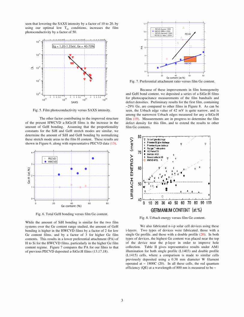
seen that lowering the SAXS intensity by a factor of 10 to 20, by using our optimal low Tfil conditions, increases the film photoconductivity by a factor of 50.
10-8
10-7
10-6
10-5
10-4
s L
10232 3 4 5 6
10242 3 4 5 6
10252 3 4 5 6
1026
SAXS
Eg = 1.20-1.35eV, Ge = 40-70%
Fig. 5. Film photoconductivity versus SAXS intensity.
The other factor contributing to the improved structure of the present HWCVD a-SiGe:H films is the increase in the amount of GeH bonding. Assuming that the proportionality constants for the SiH and GeH stretch modes are similar, we determine the amount of SiH and GeH bonding by normalizing these stretch mode areas to the film H content. These results are shown in Figure 6, along with representative PECVD data (13).
4
3
2
1
0
Ge-H
(at
.%)
806040200Ge content (%)
PECVDHWCVD
Fig. 6. Total GeH bonding versus film Ge content.
While the amount of SiH bonding is similar for the two film systems over the Ge content range studied, the amount of GeH bonding is higher in the HWCVD films by a factor of 2 for low Ge content films, and by a factor of 3 for higher Ge film contents. This results in a lower preferential attachment (PA) of H to Si for the HWCVD films, particularly in the higher Ge film content regime. Figure 7 compares the PA for our films to that of previous PECVD deposited a-SiGe:H films (13,17,18).
12
10
8
6
4
2
0
PA
806040200Ge content (at.%)
PECVD
HWCVD
PECVD (Kyoto) 1999HWCVD (NREL) 2004 PECVD (Harvard) 1990PECVD (U. Nebr.) 2004
Fig. 7. Preferential attachment ratio versus film Ge content.
Because of these improvements in film homogeneity and GeH bond content, we deposited a series of a-SiGe:H films for photocapacitance measurements of the film bandtails and defect densities. Preliminary results for the first film, containing ~29% Ge, are compared to other films in Figure 8. As can be seen, the Urbach edge value of 42 mV is quite narrow, and is among the narrowest Urbach edges measured for any a-SiGe:H film (19). Measurements are in progress to determine the film defect density for this film, and to extend the results to other film Ge contents.
Fig. 8. Urbach energy versus film Ge content.
We also fabricated n-i-p solar cell devices using these i-layers. Two types of devices were fabricated, those with a single Ge profile, and those with a double profile (20). In both types of devices, the highest Ge content was placed near the top of the device near the p-layer in order to improve hole collection. Table II gives representative results under AM1 illumination for both single profile (L1403) and double profile (L1415) cells, where a comparison is made to similar cells previously deposited using a 0.38 mm diameter W filament operated at ~ 1800C (20). In all these cells, the red quantum efficiency (QE) at a wavelength of 800 nm is measured to be ~
3

Single (Ref. 20)
Single L1403
Double (Ref. 20)
Double L1415
Voc (mV) .556 .601 .620 .625 Jsc (mA/cm2) 19.59 19.59 20.03 20.91
FF (%) .56 .549 .48 .536 h (%) 6.10 6.47 5.95 7.00
Table II.
40%. Table II shows an improvement in both types of grading structures. This has been achieved in spite of oxygen contamination in the L1403 and L1415 device i-layers. Figure 9 shows a SIMS O depth profile for a film with ~ 65 at.% Ge which is likely similar to the other recent devices. Most likely, our house hydrogen has recently contained trace amounts of oxygen, a problem that did not exist when the devices of Ref. 20 were made. At that earlier time, SIMS oxygen depth profiles indicated a very low oxygen level in our films (< 1 x 1018 cm-3), However, SIMS profiles taken on other films, deposited at other times using identical deposition conditions, can show significantly higher contamination levels. From an earlier study
-3relating to a-Si:H, oxygen levels exceeding 1-2 x 1019 cm would be expected to significantly affect device performance (21). We are currently installing purifiers on the H2 gas lines to the deposition system. This should allow us to better evaluate the device quality of the low Tfil Ta wire HWCVD material.
Figure 9. SIMS depth profiles of selected elements for a film containing 65 at.% Ge, measured during the time device fabrication was ongoing.
Acknowledgements
The work at NREL is funded by the US DOE under subcontract number DE-AC36-99-GO10337. The authors thank Q. Wang for helpful discussions.
References
1. S. Guha, J. Yang, A. Pawlikiew, T. Glatfeilter, R. Ross, and S.R. Ovshinsky, Appl. Phys. Lett. 54 (1989) 2330.
2. J. Fölsch, H. Stiebig, F. Finger, B. Rech, D. Lundszien, A. Lambertz, and H. Wagner, Proc. 25th PVSC IEEE Conference, Washington, D.C. (1996) 1133.
3. A.H. Mahan, J. Carapella, B.P. Nelson, R.S. Crandall, and I. Balberg, J. Appl. Phys. 69 (1991) 6728.
4. A.H. Mahan, R.C. Reedy, E. Iwaniczko, Q. Wang, B.P. Nelson, Y. Xu, A.C. Gallagher, H.M. Branz, R.S. Crandall, J. Yang, and S. Guha, MRS Symp. Proc. 507 (1998) 119.
5. Y. Xu, B.P. Nelson, D.L. Williamson, L.M. Gedvilas, and R.C. Reedy, MRS Symp. Proc. 762 (2003) 455.
6. A.H. Mahan, Y. Xu, and L.M. Gedvilas, MRS Symp. Proc. 808 (2004) 407.
7. Y. Xu, B.P. Nelson, L.M. Gedvilas, and R.C. Reedy, Thin Solid Films 430 (2003) 197-201.
8. M.K. van Veen, Ph.D. Thesis (Utrecht University, 2003).
9. Q. Wang, private communication. 10. Y. Hishikawa, N. Nakamura, S. Tsuda, S. Nakano, Y.
Kishi, and Y. Kuwano, Jpn. J. Appl. Phys. 30 (1991) 1008.
11. Y. Xu, L.M. Gedvilas, R.C. Reedy, H.M. Branz and A.H. Mahan, Proc. 3rd Intl. Conf. on Hot-Wire CVD (Cat-CVD) Process, Utrecht, The Netherlands, 2004, to be published in Thin Solid Films.
12. A.H. Mahan, P. Raboisson, D.L. Williamson, and R. Tsu, Solar Cells 21 (1987) 117.
13. A. Terakawa, Ph.D. Thesis, Kyoto University (1999). 14. J. Folsch, F. Finger, T. Kulessa, F. Siebke, W. Beyer,
and H. Wagner, MRS Symp. Proc. 377 (1995) 517. 15. Y-P. Chou and S-C. Lee, J. Appl. Phys. 83 (1998)
4111. 16. D.L. Williamson, NREL Report SR-520-31908 (2002)
37. 17. Y-M. Li, Ph.D. Thesis, Harvard University (1990). 18. R.J. Soukup, N.J. Ianno, S.A. Darveau, and C.L.
Exstrom. MRS Symp. Proc. 808 (2004) 359. 19. J.D. Cohen, EMIS Data Review Series 19 (1998) 180. 20. Y. Xu, B. Yan, B.P. Nelson, E. Iwaniczko, R.C.
Reedy, A.H. Mahan, and H.M. Branz, MRS Symp. Proc. 808 (2004) 617.
21. B. Yan, private communiction.
4
F1147-E(12/2004)
REPORT DOCUMENTATION PAGE Form Approved OMB No. 0704-0188
The public reporting burden for this collection of information is estimated to average 1 hour per response, including the time for reviewing instructions, searching existing data sources, gathering and maintaining the data needed, and completing and reviewing the collection of information. Send comments regarding this burden estimate or any other aspect of this collection of information, including suggestions for reducing the burden, to Department of Defense, Executive Services and Communications Directorate (0704-0188). Respondents should be aware that notwithstanding any other provision of law, no person shall be subject to any penalty for failing to comply with a collection of information if it does not display a currently valid OMB control number. PLEASE DO NOT RETURN YOUR FORM TO THE ABOVE ORGANIZATION. 1. REPORT DATE (DD-MM-YYYY)
February 2005 2. REPORT TYPE
Conference Paper 3. DATES COVERED (From - To)
3-7 January 2005 5a. CONTRACT NUMBER
DE-AC36-99-GO10337
5b. GRANT NUMBER
4. TITLE AND SUBTITLE a-SiGe:H Materials and Devices Deposited by Hot Wire CVD Using a Tantalum Filament Operated at Low Temperature
5c. PROGRAM ELEMENT NUMBER
5d. PROJECT NUMBER NREL/CP-520-37475
5e. TASK NUMBER PVA54201
6. AUTHOR(S) A.H. Mahan, Y. Xu, L.M. Gedvilas, R.C. Reedy, D.L. Williamson, S. Datta, J.D. Cohen, B. Yan, and H.M. Branz
5f. WORK UNIT NUMBER
7. PERFORMING ORGANIZATION NAME(S) AND ADDRESS(ES) National Renewable Energy Laboratory 1617 Cole Blvd. Golden, CO 80401-3393
8. PERFORMING ORGANIZATION REPORT NUMBER NREL/CP-520-37475
10. SPONSOR/MONITOR'S ACRONYM(S) NREL
9. SPONSORING/MONITORING AGENCY NAME(S) AND ADDRESS(ES)
11. SPONSORING/MONITORING AGENCY REPORT NUMBER
12. DISTRIBUTION AVAILABILITY STATEMENT National Technical Information Service U.S. Department of Commerce 5285 Port Royal Road Springfield, VA 22161
13. SUPPLEMENTARY NOTES
14. ABSTRACT (Maximum 200 Words) We report the deposition of improved hydrogenated amorphous silicon germanium (a-SiGe:H) films by the hot wire CVD (HWCVD) technique using a tantalum filament operating at a low temperature. We gauge the material quality of the a-SiGe:H films by comparing infrared, small angle X-ray scattering (SAXS), photocapacitance, and conductivity measurements to earlier results, and fabricate single-junction n-i-p solar cell devices using these i-layers.
15. SUBJECT TERMS PV; hot-wire chemical vapor deposition (HWCVD); tantalum filament; low temperature; small-angle X-ray scattering (SAXS); photocapacitance; solar cells;
16. SECURITY CLASSIFICATION OF: 19a. NAME OF RESPONSIBLE PERSON a. REPORT
Unclassified b. ABSTRACT Unclassified
c. THIS PAGE Unclassified
17. LIMITATION OF ABSTRACT
UL
18. NUMBER OF PAGES
19b. TELEPHONE NUMBER (Include area code)
Standard Form 298 (Rev. 8/98) Prescribed by ANSI Std. Z39.18