ac/dc converter ics, power factor correction (pfc ......sge0001 mar. 18, 2019 p.1 ac/dc converter...
TRANSCRIPT
P.1 SGE0001 Mar. 18, 2019
AC/DC Converter
Power Factor Control (PFC) IC
SANKEN ELECTRIC CO.,LTD
All the contents in this document are as of date of publication. Make sure that this is the latest revision of the document before use. Please check the details of the product by data sheet. https://www.sanken-ele.co.jp/en
Selection Guide
P.2 SGE0001 Mar. 18, 2019
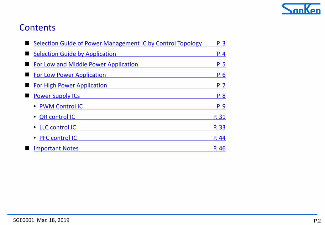
Selection Guide of Power Management IC by Control Topology P. 3 Selection Guide by Application P. 4 For Low and Middle Power Application P. 5 For Low Power Application P. 6 For High Power Application P. 7 Power Supply ICs P. 8
• PWM Control IC P. 9 • QR control IC P. 31 • LLC control IC P. 33 • PFC control IC P. 44
Important Notes P. 46
Contents
P.3 SGE0001 Mar. 18, 2019
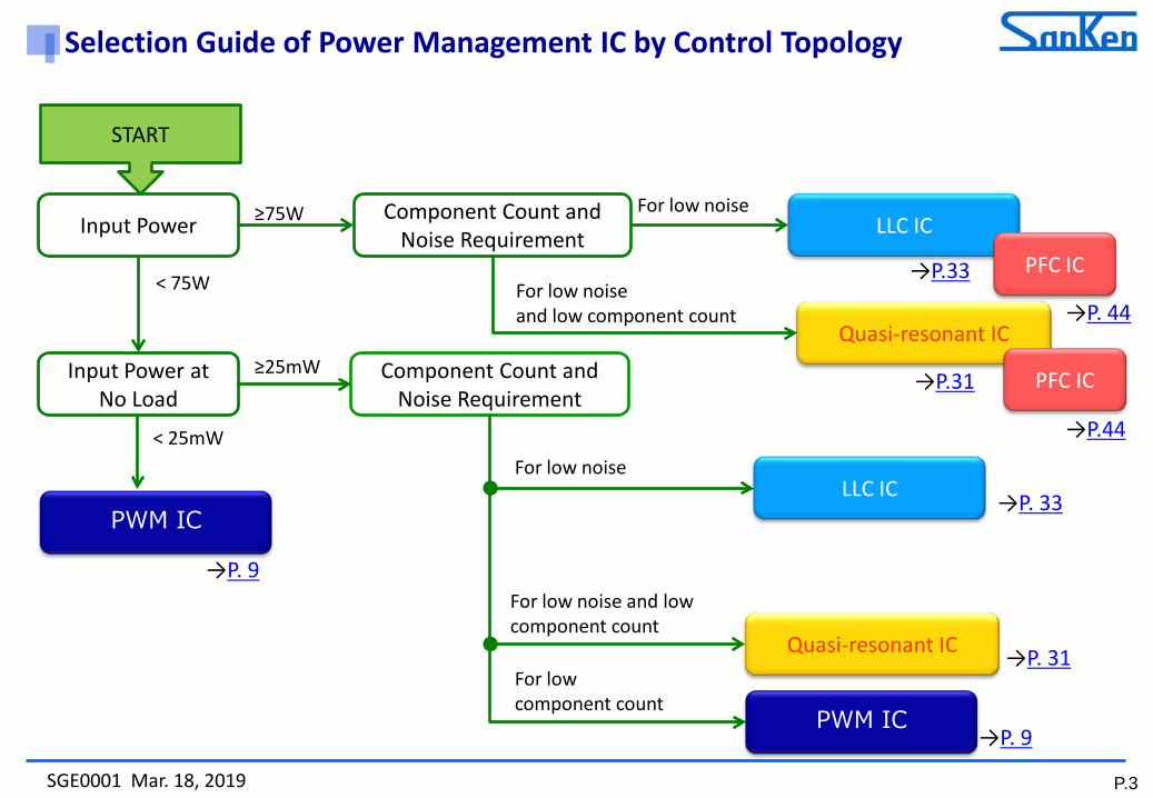
Input Power
< 75W
≥75W
Input Power at No Load
PWM IC
< 25mW
Component Count and Noise Requirement
LLC IC
Quasi-resonant IC For low component count
PWM IC
Component Count and Noise Requirement
For low noise LLC IC
For low noise and low component count
Quasi-resonant IC
PFC IC
PFC IC
START
≥25mW
For low noise
For low noise and low component count
→P. 9
→P.33
→P. 44
→P. 31
→P. 9
→P.31
→P. 33
→P.44
Selection Guide of Power Management IC by Control Topology
P.4 SGE0001 Mar. 18, 2019
Back to contents
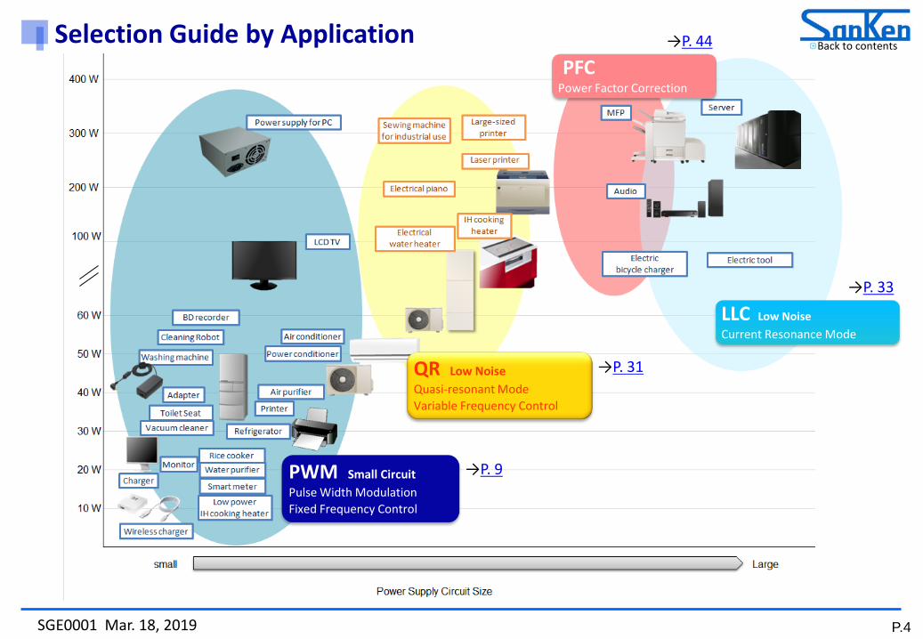
PFC Power Factor Correction
PWM Small Circuit Pulse Width Modulation Fixed Frequency Control
QR Low Noise Quasi-resonant Mode Variable Frequency Control
LLC Low Noise Current Resonance Mode
→P. 9
→P. 31
→P. 33
→P. 44 Selection Guide by Application
P.5 SGE0001 Mar. 18, 2019
Power Management IC
VAC
Cont.
Photo lsolator
FB GND
VOUT
GND
Error Amp.
PWM IC
Diode for Snubber
Diode for Secondary Rectification
QR IC
Off-line Controllers For low power application: Auxiliary power supply, white goods and adapter, etc.
For middle power application: White goods and OA etc.
Back to contents
→P. 31
→P. 9
*See Selection Guide of Diode about peripheral diodes.
For Low and Middle Power Application OFF-line Controllers with Integrated Power MOSFET and the Peripheral Diodes
P.6 SGE0001 Mar. 18, 2019
AC/DC Convertor
VAC Cont.
VOUT
(-)
(+)
AC/DC Convertor
VAC Cont.
VOUT
(-)
(+)
PWM IC Power supply for small consumer electronics and motor control, and auxiliary power supply for lighting etc.
Off-line Controllers
Freewheel Diode
→STR5A460 Series P. 27 → STR5A450 Series P. 29
Buck Converter Inverting Converter
*See Selection Guide of Diode about peripheral diodes.
Back to contents
For Low Power Application OFF-line Controllers with Integrated Power MOSFET and the Peripheral Diodes
P.7 SGE0001 Mar. 18, 2019
VAC
PFCControl IC
Photo lsolator
Control IC for Auxiliary power supply
VOUT2
Cont.
Photo lsolator
GNDFB
LLC Control IC
FB GND
REG
VS
Error Amp.
Error Amp.
VOUT1
Diode for PFC
Boot Strap Diode
PWM IC
LLC IC
PFC IC
For high power application, industrial equipment, etc.
Power Factor Correction Diode for Secondary
Rectification
For auxiliary power supply
Back to contents
Diode for Snubber
→P. 33
→P. 44
→P. 9
*See Selection Guide of Diode about peripheral diodes.
For High Power Application PFC and OFF-line Controllers and the Peripheral Diode
P.8 SGE0001 Mar. 18, 2019
Control Topology
Power MOSFET PO Circuit Size PIN at No
Load Noise Control Method Page #
PWM Built-in Lower Most Compact Fewest Large Fixed frequency P. 9
Quasi-resonant External Compact Fewer Low
(Bottom-on control)
Variable frequency P. 31
LLC External Higher Large Few Lowest Current resonance P. 33
Sanken provides the optimal power supply IC according to control topology. Please refer to Sanken’s website for detail information.
Power MOSFET PO Control Method Page #
PFC External ≥75W Critical Conduction Mode (CRM) Operation P. 44
Back to contents Power Supply ICs
P.9 SGE0001 Mar. 18, 2019
For low power, auxiliary power supply, white goods and adapter etc. Low standby power and low component count PWM: Pulse Width Modulation, fixed frequency control
Back to contents
DIP8 SOIC8
OFF-line PWM Controllers with Integrated Power MOSFET
Control Method Series Package fOSC No Load Power Consumption
Features Page #
Flyback (Secondary Side Regulation)
Low Noise in High Power
STR6A100MV STR6A100HVD DIP8 67kHz/100kHz < 15 mW Selectable Standby Operation Point .
Improving Efficiency in All Load Area. P. 11
Line Voltage Protection Model
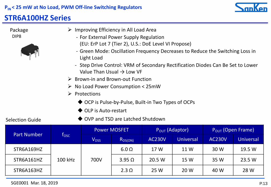
STR6A100HZ DIP8 100kHz < 25 mW Brown in / out Improving Efficiency in All Load Area. P. 13
STR-A6000xZ DIP8 67kHz/100kHz < 25 mW Brown in / out P. 15
Low Component Count Model
STR3A400 STR3A400HDL DIP8 65 kHz
100 kHz < 15 mW Low Thermal Resistance Package. Improving Efficiency in All Load Area.
P. 17 P. 19
STR3A200 DIP8 67 kHz Low Thermal Resistance Package. P. 21 STR4A100 DIP8 / SOIC8 65kHz/100kHz < 10 mW Built in OCP detection resistor P. 23
Flyback (Primary Side Regulation) STR5A100D DIP8 65 kHz < 30 mW Built in OCP detection resistor P. 25
Non-isolated Buck / Inverting
STR5A460 DIP8 / SOIC8 60 kHz ― Built in OCP detection resistor IDLIM=~0.41 A P. 27
STR5A450 DIP8 60 kHz ― Built in OCP detection resistor IO=1.2A(max.) P. 29
P.10 SGE0001 Mar. 18, 2019
White Goods, Adapter
Low Power White Goods
Maximum Output Power (Open Frame, Universal) (W)
Low Power Consumption at No Load Low Component Count Green Mode (STR5A100D)
Non-isolation Type (Buck/Inverting Converter) Low Component Count Green Mode
Aar Conditioner
Refrigerator
Adapter
Washing Machine
Microwave Oven
Cleaner
→P. 23
→P. 13
→P. 17
→P. 15
→P. 21
STR3A400*
STR6A100MV/HVD*
STR6A100HZ *
STR-A6000xZ
STR3A200
*For ErP Lot 7 (Tier 2), DoE Level VI propose
STR5A450 (Buck/Inverting Converter) →P. 29
Selectable Standby Operation Point Audible Noise Suppression in High Power
High Efficiency (Step Drive, Green Mode) →P. 11
PWM Control IC Selection Guide
→P. 27
STR4A100
STR5A100D (Primary Side Sensing) →P. 25
STR5A460 (Buck / Inverting Converter)
Low Thermal Resistance DIP8 Package Low Power Consumption at No Load Low Component Count
Line Voltage Protection (Brown-In / out)
Rice Cooker
→P. 19
10 20 30 40 50 60 70 80
STR3A400HDL*
P.11 SGE0001 Mar. 18, 2019
Part Number fOSC Power MOSFET POUT (Adaptor) POUT (Open frame) OVP, TSD
operation VDSS RDS(ON) AC230V Universal AC230V Universal
STR6A153MV 65 kHz 650 V 1.9 Ω 26 W 21 W 40 W 28 W Latched Shutdown
STR6A163HVD 100 kHz 700 V
2.3 Ω 25 W 20 W 40 W 28 W Auto-restart STR6A161HVD 3.95 Ω 20.5 W 15 W 35 W 23.5 W
STR6A169HVD 6.0 Ω 17 W 11 W 30 W 19.5 W
PIN < 15 mW at No Load, PWM Off-line Switching Regulators
Selection Guide
Improving Efficiency in All Load Area - For External Power Supply Regulation
(EU: ErP Lot 7 (Tier 2), U.S.: DoE Level VI Propose) - Green Mode: Oscillation Frequency Decreases to Reduce the Switching Loss in
Light Load - Step Drive Control: VRM of Secondary Rectification Diodes Can Be Set to Lower
Value Than Usual → Low VF
Adjustable standby operating point No Load Power Consumption < 15mW Protections OCP is Pulse-by-Pulse, Built-in two types of OCPs OLP is Auto-restart OLP and TSD are Latched Shutdown or Auto-restart
Package DIP8
UD
: Under development UD
STR6A100xV Series
P.12 SGE0001 Mar. 18, 2019
Pin No. Symbol Function
1 S/OCP Power MOSFET Source and Overcurrent Protection
2 BA Input of Selectable Standby Operation Point Signal
3 GND Ground
4 FB/OLP Feedback Control and Overload Protection
5 VCC Power supply Input and Overvoltage Protection
6 - (Pin Removed)
7 D/ST Power MOSFET Drain and Startup Current Input
8
Pin Assignment
Package DIP8
Features Step Drive Control Adjustable standby operating point Automatically Changed Operation Mode in Response to Load Conditions
- Fixed Switching Frequency Mode in normal operation (67kHz or100 kHz) . - Green Mode, 25 kHz to 67kHz or100 kHz in middle to light load. - Burst Oscillation Mode in Light Load Soft Start Function
No Load Power Consumption < 15mW Random Switching Function
Slope Compensation Function Leading Edge Blanking Function Bias Assist Function Two Chip Structure (Avalanche Energy Guaranteed) Protections
- Overcurrent Protection (OCP): Pulse-by-Pulse, Two Types of OCPs - Overload Protection (OLP): Auto-restart with Delay Timer - Overvoltage Protection (OVP): Latched Shutdown or Auto-restart - Thermal Shutdown (TSD): Latched Shutdown or Auto-restart with
Hysteresis
VAC
C1 C6 R1
D1
BR1
R2
C2
T1
D
P
PC1
C3
ROCP
CY
CRD clamp snubber
C5
C(RC)damper snubber
D2C4
D51
C51
R51
R52
U51
R54
R56
C52
S
PC1
R53
R55
L51
C53
VOUT
(-)
TC_STR6A100xV_2_R1
(+)
RBA
NC
8
7
5
STR6A100×VD
U11
2
3
4
D/ST
D/STBA
S/OCP
FB/OLP
GND
VCC
Typical Application Circuit
PIN < 15 mW at No Load, PWM Off-line Switching Regulators
STR6A100xV Series
P.13 SGE0001 Mar. 18, 2019
Package DIP8
PIN < 25 mW at No Load, PWM Off-line Switching Regulators
Part Number fOSC Power MOSFET POUT (Adaptor) POUT (Open Frame)
VDSS RDS(ON) AC230V Universal AC230V Universal
STR6A169HZ
100 kHz 700V
6.0 Ω 17 W 11 W 30 W 19.5 W
STR6A161HZ 3.95 Ω 20.5 W 15 W 35 W 23.5 W
STR6A163HZ 2.3 Ω 25 W 20 W 40 W 28 W
Selection Guide
Improving Efficiency in All Load Area - For External Power Supply Regulation
(EU: ErP Lot 7 (Tier 2), U.S.: DoE Level VI Propose) - Green Mode: Oscillation Frequency Decreases to Reduce the Switching Loss in
Light Load - Step Drive Control: VRM of Secondary Rectification Diodes Can Be Set to Lower
Value Than Usual → Low VF Brown-in and Brown-out Function No Load Power Consumption < 25mW Protections OCP is Pulse-by-Pulse, Built-in Two Types of OCPs OLP is Auto-restart OVP and TSD are Latched Shutdown
STR6A100HZ Series
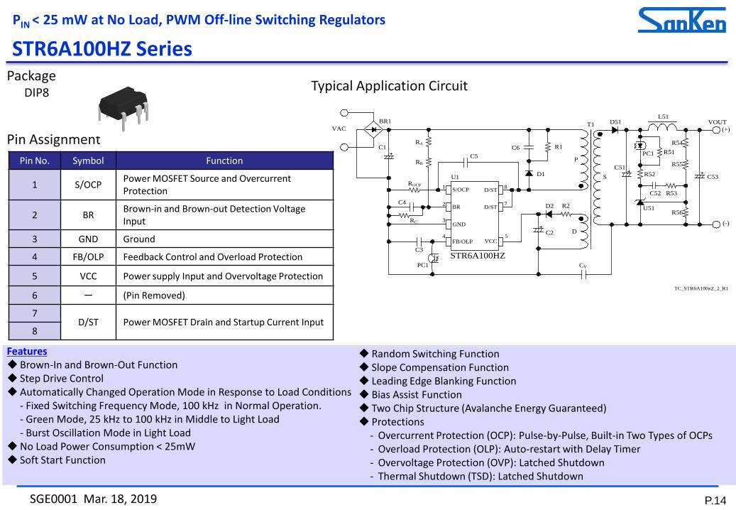
P.14 SGE0001 Mar. 18, 2019
Pin No. Symbol Function
1 S/OCP Power MOSFET Source and Overcurrent Protection
2 BR Brown-in and Brown-out Detection Voltage Input
3 GND Ground
4 FB/OLP Feedback Control and Overload Protection
5 VCC Power supply Input and Overvoltage Protection
6 - (Pin Removed)
7 D/ST Power MOSFET Drain and Startup Current Input
8
Pin Assignment
Package DIP8
VAC
C1 C6 R1
D1
BR1
R2
C2
T1
D
P
PC1
C3
ROCP
CY
C5
D2C4
D51
C51
R51
R52
U51
R54
R56
C52
S
PC1
R53
R55
L51
C53
VOUT
(-)
(+)
RC
NC
8
7
5
STR6A100HZ
U11
2
3
4
D/ST
D/STBR
S/OCP
FB/OLP
GND
VCC
RA
RB
TC_STR6A100xZ_2_R1
PIN < 25 mW at No Load, PWM Off-line Switching Regulators
Typical Application Circuit
Features Brown-In and Brown-Out Function Step Drive Control Automatically Changed Operation Mode in Response to Load Conditions
- Fixed Switching Frequency Mode, 100 kHz in Normal Operation. - Green Mode, 25 kHz to 100 kHz in Middle to Light Load - Burst Oscillation Mode in Light Load
No Load Power Consumption < 25mW Soft Start Function
Random Switching Function Slope Compensation Function Leading Edge Blanking Function Bias Assist Function Two Chip Structure (Avalanche Energy Guaranteed) Protections
- Overcurrent Protection (OCP): Pulse-by-Pulse, Built-in Two Types of OCPs - Overload Protection (OLP): Auto-restart with Delay Timer - Overvoltage Protection (OVP): Latched Shutdown - Thermal Shutdown (TSD): Latched Shutdown
STR6A100HZ Series
P.15 SGE0001 Mar. 18, 2019
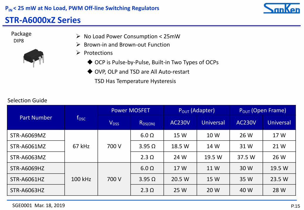
PIN < 25 mW at No Load, PWM Off-line Switching Regulators
Part Number fOSC Power MOSFET POUT (Adapter) POUT (Open Frame)
VDSS RDS(ON) AC230V Universal AC230V Universal
STR-A6069MZ
67 kHz 700 V
6.0 Ω 15 W 10 W 26 W 17 W
STR-A6061MZ 3.95 Ω 18.5 W 14 W 31 W 21 W
STR-A6063MZ 2.3 Ω 24 W 19.5 W 37.5 W 26 W
STR-A6069HZ
100 kHz 700 V
6.0 Ω 17 W 11 W 30 W 19.5 W
STR-A6061HZ 3.95 Ω 20.5 W 15 W 35 W 23.5 W
STR-A6063HZ 2.3 Ω 25 W 20 W 40 W 28 W
Selection Guide
No Load Power Consumption < 25mW Brown-in and Brown-out Function Protections OCP is Pulse-by-Pulse, Built-in Two Types of OCPs OVP, OLP and TSD are All Auto-restart
TSD Has Temperature Hysteresis
Package DIP8
STR-A6000xZ Series
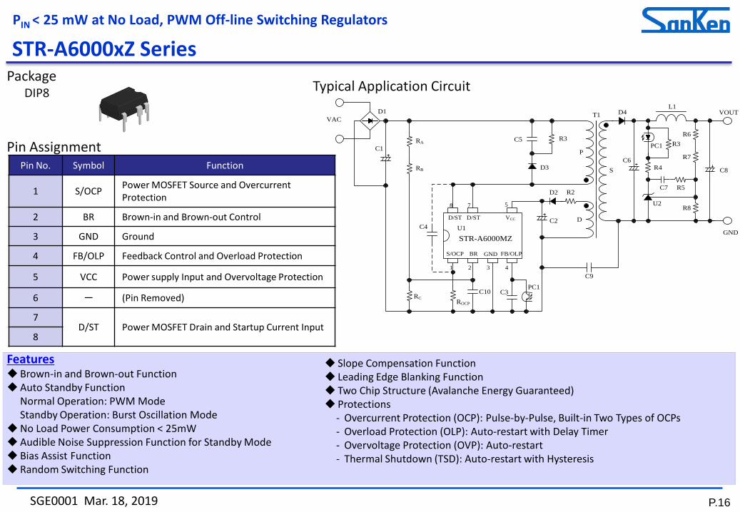
P.16 SGE0001 Mar. 18, 2019
VAC
C1C5 R3
D3
D1
R2
C2
T1
D
P
PC1C3
ROCP
C9
C4
1 2 3 4
D/ST D/ST
BR
NC
S/OCP FB/OLPGND
VCC
8 7 5
STR-A6000MZU1
D2
C10RC
RB
RA
D4
C6
R3
R4
U2
R6
R8
C7
S
PC1
R5
R7
L1
C8
VOUT
GND
Features Brown-in and Brown-out Function Auto Standby Function
Normal Operation: PWM Mode Standby Operation: Burst Oscillation Mode
No Load Power Consumption < 25mW Audible Noise Suppression Function for Standby Mode Bias Assist Function Random Switching Function
Pin No. Symbol Function
1 S/OCP Power MOSFET Source and Overcurrent Protection
2 BR Brown-in and Brown-out Control
3 GND Ground
4 FB/OLP Feedback Control and Overload Protection
5 VCC Power supply Input and Overvoltage Protection
6 - (Pin Removed)
7 D/ST Power MOSFET Drain and Startup Current Input
8
Pin Assignment
Slope Compensation Function Leading Edge Blanking Function Two Chip Structure (Avalanche Energy Guaranteed) Protections
- Overcurrent Protection (OCP): Pulse-by-Pulse, Built-in Two Types of OCPs - Overload Protection (OLP): Auto-restart with Delay Timer - Overvoltage Protection (OVP): Auto-restart - Thermal Shutdown (TSD): Auto-restart with Hysteresis
Package DIP8
PIN < 25 mW at No Load, PWM Off-line Switching Regulators
Typical Application Circuit
STR-A6000xZ Series
P.17 SGE0001 Mar. 18, 2019
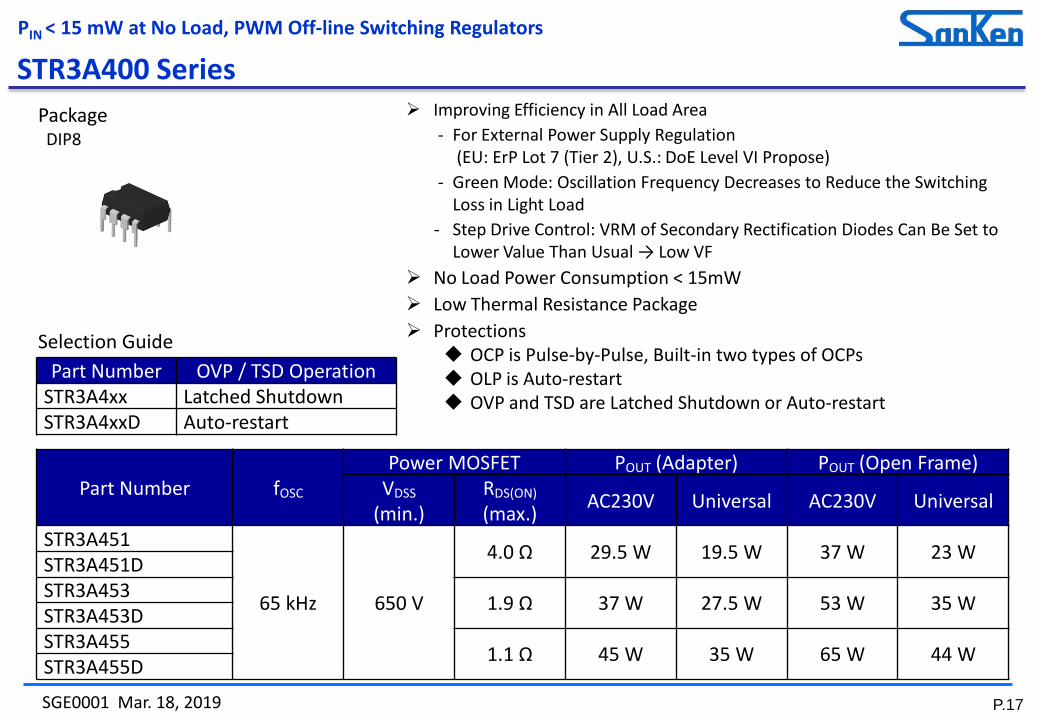
PIN < 15 mW at No Load, PWM Off-line Switching Regulators
Part Number fOSC Power MOSFET POUT (Adapter) POUT (Open Frame)
VDSS
(min.) RDS(ON) (max.) AC230V Universal AC230V Universal
STR3A451
65 kHz 650 V
4.0 Ω 29.5 W 19.5 W 37 W 23 W STR3A451D STR3A453 1.9 Ω 37 W 27.5 W 53 W 35 W STR3A453D STR3A455 1.1 Ω 45 W 35 W 65 W 44 W STR3A455D
Selection Guide
Improving Efficiency in All Load Area - For External Power Supply Regulation
(EU: ErP Lot 7 (Tier 2), U.S.: DoE Level VI Propose) - Green Mode: Oscillation Frequency Decreases to Reduce the Switching
Loss in Light Load - Step Drive Control: VRM of Secondary Rectification Diodes Can Be Set to
Lower Value Than Usual → Low VF
No Load Power Consumption < 15mW Low Thermal Resistance Package Protections
OCP is Pulse-by-Pulse, Built-in two types of OCPs OLP is Auto-restart OVP and TSD are Latched Shutdown or Auto-restart
Package DIP8
Part Number OVP / TSD Operation STR3A4xx Latched Shutdown STR3A4xxD Auto-restart
STR3A400 Series
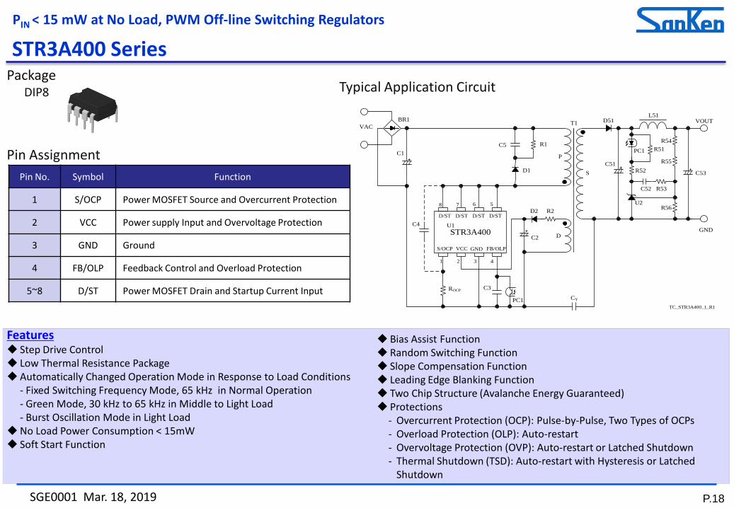
P.18 SGE0001 Mar. 18, 2019
Features Step Drive Control Low Thermal Resistance Package Automatically Changed Operation Mode in Response to Load Conditions
- Fixed Switching Frequency Mode, 65 kHz in Normal Operation - Green Mode, 30 kHz to 65 kHz in Middle to Light Load - Burst Oscillation Mode in Light Load
No Load Power Consumption < 15mW Soft Start Function
Pin No. Symbol Function
1 S/OCP Power MOSFET Source and Overcurrent Protection
2 VCC Power supply Input and Overvoltage Protection
3 GND Ground
4 FB/OLP Feedback Control and Overload Protection
5~8 D/ST Power MOSFET Drain and Startup Current Input
Pin Assignment
Bias Assist Function Random Switching Function Slope Compensation Function Leading Edge Blanking Function Two Chip Structure (Avalanche Energy Guaranteed) Protections
- Overcurrent Protection (OCP): Pulse-by-Pulse, Two Types of OCPs - Overload Protection (OLP): Auto-restart - Overvoltage Protection (OVP): Auto-restart or Latched Shutdown - Thermal Shutdown (TSD): Auto-restart with Hysteresis or Latched
Shutdown
Package DIP8
PIN < 15 mW at No Load, PWM Off-line Switching Regulators
Typical Application Circuit
VAC
C1C5 R1
D1
D2 R2
C2
T1 D51
C51
R51
R52
U2
R54
R56
C52
D
P
S
PC1
PC1
C3ROCP
BR1
R53
R55
L51
C53
C4
VOUT
GND
1 2 3 4
D/ST D/ST
VCC
NC
S/OCP FB/OLPGND
D/ST D/ST
8 7 6 5
STR3A400U1
CY
TC_STR3A400_1_R1
STR3A400 Series
P.19 SGE0001 Mar. 18, 2019
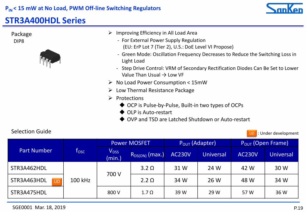
PIN < 15 mW at No Load, PWM Off-line Switching Regulators
Selection Guide
Improving Efficiency in All Load Area - For External Power Supply Regulation
(EU: ErP Lot 7 (Tier 2), U.S.: DoE Level VI Propose) - Green Mode: Oscillation Frequency Decreases to Reduce the Switching Loss in
Light Load - Step Drive Control: VRM of Secondary Rectification Diodes Can Be Set to Lower
Value Than Usual → Low VF
No Load Power Consumption < 15mW Low Thermal Resistance Package Protections
OCP is Pulse-by-Pulse, Built-in two types of OCPs OLP is Auto-restart OVP and TSD are Latched Shutdown or Auto-restart
Package DIP8
STR3A400HDL Series
Part Number fOSC Power MOSFET POUT (Adapter) POUT (Open Frame)
VDSS
(min.) RDS(ON) (max.) AC230V Universal AC230V Universal
STR3A462HDL
100 kHz 700 V
3.2 Ω 31 W 24 W 42 W 30 W
STR3A463HDL 2.2 Ω 34 W 26 W 48 W 34 W
STR3A475HDL 800 V 1.7 Ω 39 W 29 W 57 W 36 W
: Under development UD
UD
P.20 SGE0001 Mar. 18, 2019
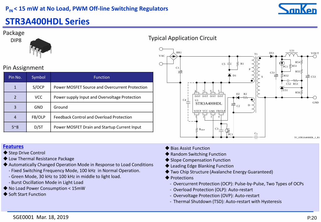
Features Step Drive Control Low Thermal Resistance Package Automatically Changed Operation Mode in Response to Load Conditions
- Fixed Switching Frequency Mode, 100 kHz in Normal Operation. - Green Mode, 30 kHz to 100 kHz in middle to light load. - Burst Oscillation Mode in Light Load
No Load Power Consumption < 15mW Soft Start Function
Pin No. Symbol Function
1 S/OCP Power MOSFET Source and Overcurrent Protection
2 VCC Power supply Input and Overvoltage Protection
3 GND Ground
4 FB/OLP Feedback Control and Overload Protection
5~8 D/ST Power MOSFET Drain and Startup Current Input
Pin Assignment
Bias Assist Function Random Switching Function Slope Compensation Function Leading Edge Blanking Function Two Chip Structure (Avalanche Energy Guaranteed) Protections
- Overcurrent Protection (OCP): Pulse-by-Pulse, Two Types of OCPs - Overload Protection (OLP): Auto-restart - Overvoltage Protection (OVP): Auto-restart - Thermal Shutdown (TSD): Auto-restart with Hysteresis
Package DIP8
PIN < 15 mW at No Load, PWM Off-line Switching Regulators
Typical Application Circuit
STR3A400HDL Series
VAC
C1C5 R1
D1
D2 R2
C2
T1 D51
C51
R51
R52
U51
R54
R56
C52
D
P
S
PC1
PC1
C3ROCP
BR1
R53
R55
L51
C53
C4
VOUT
GND
1 2 3 4
D/ST D/ST
VCC
NC
S/OCP FB/OLPGND
D/ST D/ST
8 7 6 5
STR3A400HDLU1
CY
TC_STR3A400HDL_1_R1
P.21 SGE0001 Mar. 18, 2019
PIN < 15 mW at No Load, PWM Off-line Switching Regulators
Part Number fOSC(AVG) Power MOSFET POUT (Adapter) POUT (Open Frame)
VDSS RDS(ON) AC230V Universal AC230V Universal STR3A251
67 kHz 650 V
4.0 Ω 29.5 W 19.5 W 37 W 23 W STR3A251D STR3A253
1.9 Ω 37 W 27.5 W 53 W 35 W STR3A253D STR3A255
1.1 Ω 45 W 35 W 65 W 44 W STR3A255D
Selection Guide
No Load Power Consumption < 15mW Low Thermal Resistance Package Protections OCP is Pulse-by-Pulse, Built-in Two Types of OCPs OLP is Auto-restart OVP is Auto-restart or Latched Shutdown TSD is Auto-restart with Temperature Hysteresis or Latched Shutdown
Part Number OVP / TSD Operation STR3A2xx Latched Shutdown STR3A2xxD Auto-restart
Package DIP8
UD
UD
UD
: Under development UD
STR3A200 Series
P.22 SGE0001 Mar. 18, 2019
Features Low Thermal Resistance Package Soft Start Function Operation Mode
Normal Operation: PWM Mode Standby Operation: Burst Oscillation Mode
No Load Power Consumption < 15mW Random Switching Function
Pin No. Symbol Function
1 S/OCP Power MOSFET Source and Overcurrent Protection
2 VCC Power supply Input and Overvoltage Protection
3 GND Ground
4 FB/OLP Feedback Control and Overload Protection
5
D/ST Power MOSFET Drain and Startup Current Input 6
7
8
Pin Assignment
Slope Compensation Function Leading Edge Blanking Function Bias Assist Function Two Chip Structure (Avalanche Energy Guaranteed) Protections
- Overcurrent Protection (OCP): Pulse-by-Pulse, Built-in Two Types of OCPs - Overload Protection (OLP): Auto-restart with Delay Timer - Overvoltage Protection (OVP): Latched Shutdown or Auto-restart - Thermal Shutdown (TSD): Latched Shutdown or Auto-restart with Hysteresis
Package DIP8
PIN < 15 mW at No Load, PWM Off-line Switching Regulators
VAC
C1C5 R1
D1
D2 R2
C2
T1 D51
C51
R51
R52
U2
R54
R56
C52
D
P
S
PC1
PC1
C3ROCP
BR1
R53
R55
L51
C53
C4
VOUT
GND
1 2 3 4
D/ST D/ST
VCC
NC
S/OCP FB/OLPGND
D/ST D/ST
8 7 6 5
STR3A200U1
CY
Typical Application Circuit
STR3A200 Series
P.23 SGE0001 Mar. 18, 2019
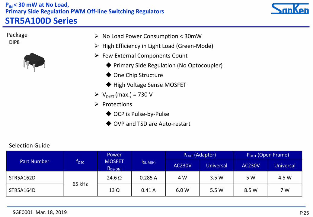
No Load Power Consumption < 10 mW High Voltage Sense MOSFET One Chip Structure (Eliminating External Components) VD/ST (max.) = 730 V Protections OCP is Pulse-by-Pulse OVP, OLP and TSD are All Auto-restart
Part Number Package fOSC Power MOSFET RDS(ON)
IDLIM(H)
POUT (Adapter) POUT (Open Frame)
AC230V Universal AC230V Universal
STR4A162S SOIC8
65 kHz 24.6 Ω 0.365 A
5 W 4 W 7 W 5.5 W
STR4A162D DIP8 5.5 W 4.5 W 7.5 W 6 W
STR4A164D DIP8 12.9 Ω 0.520 A 8 W 6 W 10 W 8.5 W
STR4A164HD DIP8 100 kHz 12.9 Ω 0.485 A 9 W 7 W 13 W 10.5 W
PIN < 10 mW at No Load, PWM Off-line Switching Regulators
Selection Guide
Package DIP8 SOIC8
STR4A100 Series
P.24 SGE0001 Mar. 18, 2019
Pin No. Symbol Function
1 FB/OLP Feedback Control and Overload Protection
2 VCC Power supply Input and Overvoltage Protection
3 ― (Pin Removed)
4 D/ST Power MOSFET Drain and Startup Current Input
5
S/GND Power MOSFET Source and Ground 6
7
8
Pin Assignment
Features High Voltage Sense MOSFET One Chip Structure (Eliminating External Components) Auto Standby Function
Normal Operation: PWM Mode Standby Operation: Burst Oscillation Mode
No Load Power Consumption < 10 mW Soft Start Function Bias Assist Function
Random Switching Function Slope Compensation Function Leading Edge Blanking Function Protections
- Overcurrent Protection (OCP): Pulse-by-Pulse, with Input Compensation Circuit
- Overload Protection (OLP): Auto-restart with Delay Timer - Overvoltage Protection (OVP): Auto-restart - Thermal Shutdown (TSD): Auto-restart
PIN < 10 mW at No Load, PWM Off-line Switching Regulators
Typical Application Circuit Package DIP8 SOIC8
STR4A100 Series
P.25 SGE0001 Mar. 18, 2019
Part Number fOSC Power
MOSFET RDS(ON)
IDLIM(H)
POUT (Adapter) POUT (Open Frame)
AC230V Universal AC230V Universal
STR5A162D 65 kHz
24.6 Ω 0.285 A 4 W 3.5 W 5 W 4.5 W
STR5A164D 13 Ω 0.41 A 6.0 W 5.5 W 8.5 W 7 W
PIN < 30 mW at No Load, Primary Side Regulation PWM Off-line Switching Regulators
No Load Power Consumption < 30mW High Efficiency in Light Load (Green-Mode) Few External Components Count Primary Side Regulation (No Optocoupler) One Chip Structure High Voltage Sense MOSFET
VD/ST (max.) = 730 V Protections OCP is Pulse-by-Pulse OVP and TSD are Auto-restart
Selection Guide
Package DIP8
STR5A100D Series
P.26 SGE0001 Mar. 18, 2019
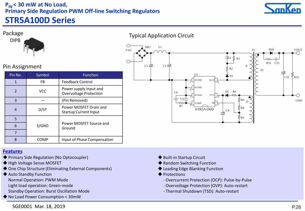
Pin Assignment
Features Primary Side Regulation (No Optocoupler) High Voltage Sense MOSFET One Chip Structure (Eliminating External Components) Auto Standby Function
Normal Operation: PWM Mode Light load operation: Green-mode Standby Operation: Burst Oscillation Mode
No Load Power Consumption < 30mW
Built-in Startup Circuit Random Switching Function Leading Edge Blanking Function Protections
- Overcurrent Protection (OCP): Pulse-by-Pulse - Overvoltage Protection (OVP): Auto-restart - Thermal Shutdown (TSD): Auto-restart
Pin No. Symbol Function
1 FB Feedback Control
2 VCC Power supply Input and Overvoltage Protection
3 ― (Pin Removed)
4 D/ST Power MOSFET Drain and Startup Current Input
5
S/GND Power MOSFET Source and Ground 6
7
8 COMP Input of Phase Compensation
Package DIP8
PIN < 30 mW at No Load, Primary Side Regulation PWM Off-line Switching Regulators
VAC
C1
R1
D1
T1
D
P
C5
C4
C3
R6
R3
R5
D2
BR1
COMP
S/GND VCC
NC
FB
D/ST
S/GND
S/GND
8
7
6
5
STR5A100D
U1
1
2
4
R2
L1
C2
R4
D50
S1
VOUT
GND
C52
C51R51
C6
R7
R52
Typical Application Circuit
STR5A100D Series
P.27 SGE0001 Mar. 18, 2019
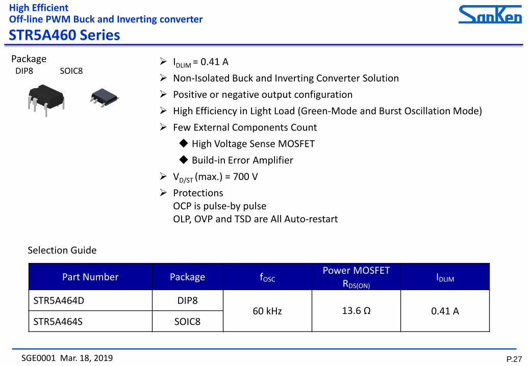
IDLIM = 0.41 A Non-Isolated Buck and Inverting Converter Solution Positive or negative output configuration High Efficiency in Light Load (Green-Mode and Burst Oscillation Mode) Few External Components Count High Voltage Sense MOSFET Build-in Error Amplifier
VD/ST (max.) = 700 V Protections
OCP is pulse-by pulse OLP, OVP and TSD are All Auto-restart
Part Number Package fOSC Power MOSFET RDS(ON)
IDLIM
STR5A464D DIP8 60 kHz 13.6 Ω 0.41 A
STR5A464S SOIC8
Selection Guide
High Efficient Off-line PWM Buck and Inverting converter
Package DIP8 SOIC8
STR5A460 Series
P.28 SGE0001 Mar. 18, 2019
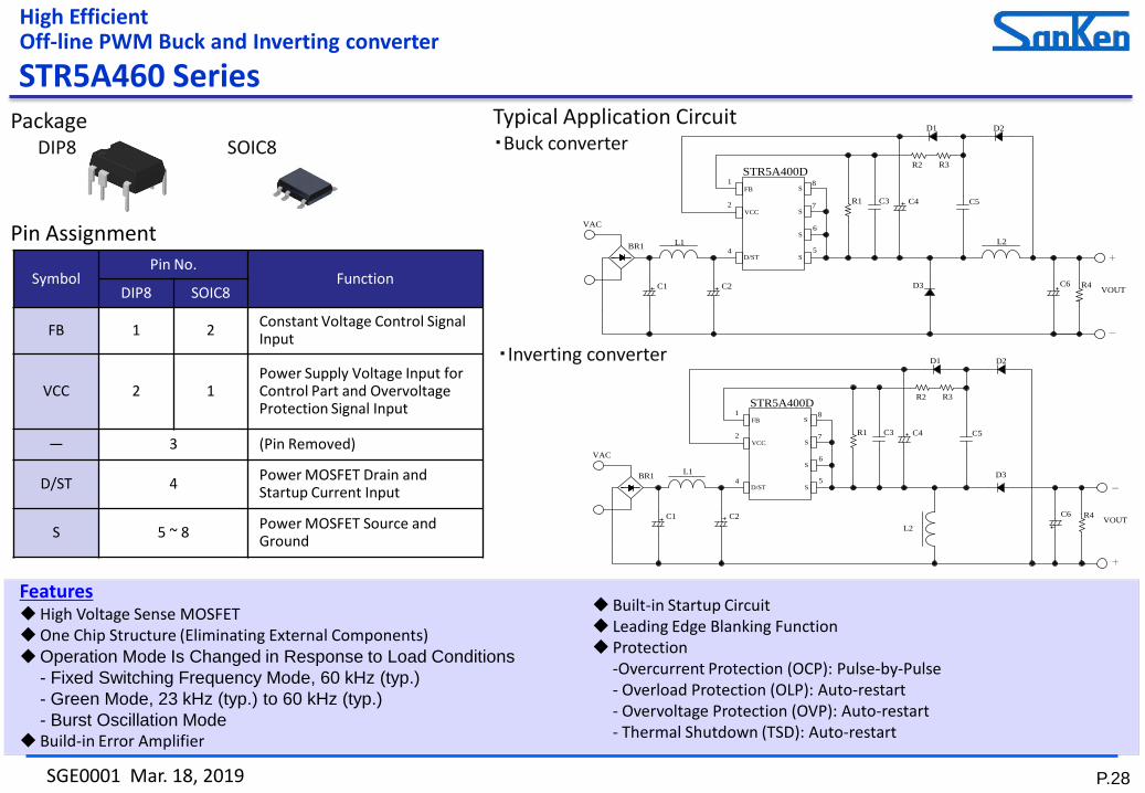
Pin Assignment
Typical Application Circuit ・Buck converter
Features High Voltage Sense MOSFET One Chip Structure (Eliminating External Components) Operation Mode Is Changed in Response to Load Conditions
- Fixed Switching Frequency Mode, 60 kHz (typ.) - Green Mode, 23 kHz (typ.) to 60 kHz (typ.) - Burst Oscillation Mode
Build-in Error Amplifier
Built-in Startup Circuit Leading Edge Blanking Function Protection
-Overcurrent Protection (OCP): Pulse-by-Pulse - Overload Protection (OLP): Auto-restart - Overvoltage Protection (OVP): Auto-restart - Thermal Shutdown (TSD): Auto-restart
VAC
VOUT
SVCC
NC
FB
D/ST
S
S
8
7
6
5
STR5A400D
4
2
1
C2
C4R1 C3
R2 R3
C5
C6 R4D3
D2D1
L2L1
C1
S
+
-
BR1
VOUT
SVCC
NC
FB
D/ST
S
S
8
7
6
5
STR5A400D
4
2
1
C2
C4R1 C3
R2 R3
C5
C6 R4
D3
D2D1
L2
L1
C1
S
-
+
VAC
BR1
・Inverting converter
Symbol Pin No.
Function DIP8 SOIC8
FB 1 2 Constant Voltage Control Signal Input
VCC 2 1 Power Supply Voltage Input for Control Part and Overvoltage Protection Signal Input
― 3 (Pin Removed)
D/ST 4 Power MOSFET Drain and Startup Current Input
S 5 ~ 8 Power MOSFET Source and Ground
High Efficient Off-line PWM Buck and Inverting converter
Package DIP8 SOIC8
STR5A460 Series
P.29 SGE0001 Mar. 18, 2019
Maximum Output Current is 1.2 A Non-Isolated Buck and Inverting Converter Solution High Efficiency in Light Load (Green-Mode and Burst Oscillation Mode) Few External Components Count Build-in Error Amplifier
VDSS (min.) = 650 V Protections
OCP is pulse-by pulse. OLP, OVP and TSD are All Auto-restart.
Selection Guide
High Efficient Off-line PWM Buck and Inverting converter
Package DIP8
Part Number Package fOSC Power MOSFET RDS(ON)
IOUT(MAX)
(VOUT = 24 V)
STR5A451D DIP8 60 kHz
4.0 Ω 0.7 A
STR5A453D 1.9 Ω 0.9 A
STR5A450 Series
P.30 SGE0001 Mar. 18, 2019
Pin Assignment
Typical Application Circuit ・Buck Converter
Features Operation Mode Is Changed in Response to Load Conditions,
- Fixed Switching Frequency Mode, 60 kHz (typ.) - Green Mode, 23 kHz (typ.) to 60 kHz (typ.) - Burst Oscillation Mode
Build-in Error Amplifier Built-in Startup Circuit
Leading Edge Blanking Function Protection
-Overcurrent Protection (OCP): Pulse-by-Pulse, with Input Compensation Circuit - Overload Protection (OLP): Auto-restart - Overvoltage Protection (OVP): Auto-restart - Thermal Shutdown (TSD): Auto-restart
・Inverting Converter
High Efficient Off-line PWM Buck and Inverting converter
Package DIP8
VOUT
C1
C4 R1
R2 R3
C5
C2 R4D3
D2
D1
L1(+)
(-)
VAC
TC_STR5A450_2_R1
D/ST
D/ST FB
S/OCP
VCC
D/ST
D/ST
8
7
6
5
STR5A450D
4
2
1
GND3
ROCP
C3
D2 D3
D4D1
VOUT
C1
C4 R1
R2 R3
C5
C2 R4
D3
D2
D1
L1
(+)
(-)
VAC
TC_STR5A450_3_R1
D/ST
D/ST FB
S/OCP
VCC
D/ST
D/ST
8
7
6
5
STR5A450D
4
2
1
GND3
ROCP
C3
D2 D3
D4D1
Pin No. Symbol Function
1 S/OCP Power MOSFET Source and Overcurrent Protection (OCP) Signal Input
2 FB Constant Voltage Control Signal Input
3 GND Ground
4 VCC Power Supply Voltage Input for Control Part and Overvoltage Protection (OVP) Signal Input
5
D/ST Power MOSFET Drain and Startup Current Input
6
7
8
STR5A450 Series
P.31 SGE0001 Mar. 18, 2019
For Middle Power Application: White Goods and OA, Etc. High Efficiency Operation Across the Full Range of Loads Is Achieved by Multi-Mode Control Low Noise Due to Bottom on Switching
Back to contents
Off-line Quasi-resonant (QR) Controllers
Series Package Features Page #
SSC1S311A SSC1S312A
SOIC8
Low Power Consumption at No Load ( < 30 mW) Few External Components Count (Built-in Startup Circuit) P. 32
P.32 SGE0001 Mar. 18, 2019
Low Noise, No Load Power Consumption < 30mW Quasi-resonant (QR) Off-line Switching Regulators SSC1S310A Series
Features Auto standby function
No load power consumption < 30mW Auto burst function
Normal operation: Quasi-resonant Standby operation: Burst oscillation mode (1 bottom skip)
Leading edge blanking function Built-in Startup Circuit Protection functions
Overcurrent Protection (OCP): Pulse by pulse Overload Protection (OLP) Overvoltage Protection (OVP) Thermal Shutdown (TSD)
Package SOIC8
VAC
C1
D2 R2
C2
T1 D4
C6
R6
R7
U2
R9
R11
C7
D
P
S
PC1
PC1C4
ROCP
D1
R8
R10
L1
C8CV
VOUT
GND
1 2 4
GND VCC
BDFB/OLP ST
OCP DRV
8 7 6 5
SSC1S310AU1
D3 R5
R4R3
Q1
C3
RBD2
RBD1
DZBD
CBD
R1
C5
R12C9
Pin assignment Pin No. Symbol Function
1 FB/OLP Feedback control and Overload Protection signal input
2 BD Bottom detection signal input and input compensation detection signal input
3 ― (Pin removed) 4 ST Startup current input 5 DRV Gate drive output 6 OCP Overcurrent Protection signal input
7 VCC Power supply input and Overvoltage Protection signal input
8 GND Ground
Typical application circuit
Part Number OLP, OVP, TSD Operation
SSC1S311A Auto-restart
SSC1S312A Latched Shutdown
Selection Guide
P.33 SGE0001 Mar. 18, 2019
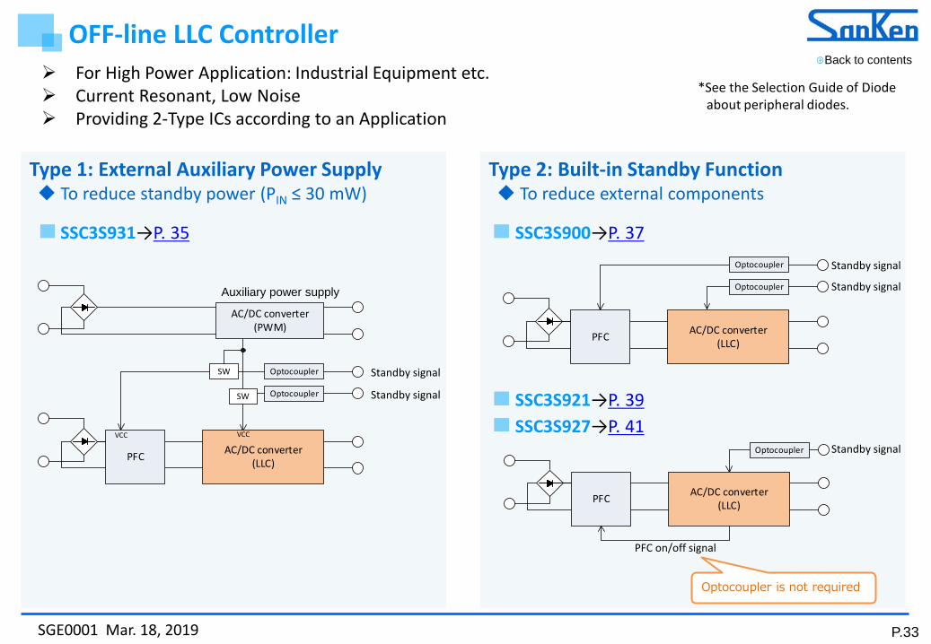
Type 2: Built-in Standby Function To reduce external components
Type 1: External Auxiliary Power Supply To reduce standby power (PIN ≤ 30 mW)
Optocoupler
AC/DC converter(PWM)
OptocouplerSW
SW
PFC
VCC
AC/DC converter(LLC)
VCC
Optocoupler
Optocoupler
PFC AC/DC converter(LLC)
Optocoupler
PFC AC/DC converter(LLC)
Back to contents For High Power Application: Industrial Equipment etc. Current Resonant, Low Noise Providing 2-Type ICs according to an Application
*See the Selection Guide of Diode about peripheral diodes.
OFF-line LLC Controller
SSC3S931→P. 35 SSC3S900→P. 37
Optocoupler is not required
SSC3S927→P. 41
Standby signal
Standby signal
Auxiliary power supply
SSC3S921→P. 39
Standby signal
Standby signal
Standby signal
PFC on/off signal
P.34 SGE0001 Mar. 18, 2019
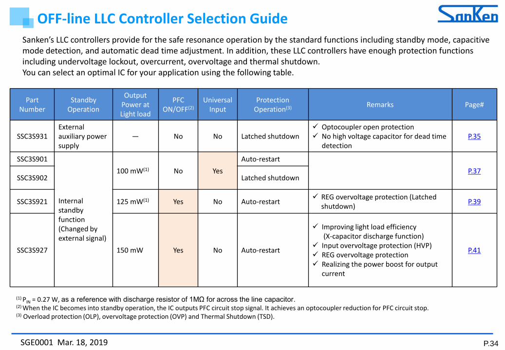
OFF-line LLC Controller Selection Guide
(1) PIN = 0.27 W, as a reference with discharge resistor of 1MΩ for across the line capacitor. (2) When the IC becomes into standby operation, the IC outputs PFC circuit stop signal. It achieves an optocoupler reduction for PFC circuit stop. (3) Overload protection (OLP), overvoltage protection (OVP) and Thermal Shutdown (TSD).
Sanken’s LLC controllers provide for the safe resonance operation by the standard functions including standby mode, capacitive mode detection, and automatic dead time adjustment. In addition, these LLC controllers have enough protection functions including undervoltage lockout, overcurrent, overvoltage and thermal shutdown. You can select an optimal IC for your application using the following table.
Part Number
Standby Operation
Output Power at Light load
PFC ON/OFF(2)
Universal Input
Protection Operation(3) Remarks Page#
SSC3S931 External auxiliary power supply
― No No Latched shutdown Optocoupler open protection No high voltage capacitor for dead time
detection P.35
SSC3S901
Internal standby function (Changed by external signal)
100 mW(1) No Yes Auto-restart
P.37 SSC3S902 Latched shutdown
SSC3S921 125 mW(1) Yes No Auto-restart REG overvoltage protection (Latched shutdown) P.39
SSC3S927 150 mW Yes No Auto-restart
Improving light load efficiency (X-capacitor discharge function)
Input overvoltage protection (HVP) REG overvoltage protection Realizing the power boost for output
current
P.41
P.35 SGE0001 Mar. 18, 2019
VAC
VOUT
Error Amp.
SSC3S931
GND
REG VS
PFCControl IC
Auxiliary power supply
Standby signal
SWSW
AC/DC Converter
Optocoupler
Optocoupler Standby signal
VCCGND VCC
VAC
VOUT
Error Amp.
SSC9522S
GND
REGVS
RV
PFCControl IC
Auxiliary power supply
Standby signal
SWSW
AC/DC Converter
Optocoupler
Optocoupler Standby signal
VCCGND VCC
Package SOP18
Features Floating drive circuit Soft-start Function Capacitive Mode Detection Function Reset Detection Function Automatic Dead Time Adjustment Function Protections
- High-side driver UVLO : Auto-restart - VCC Pin Overvoltage Protection (VCC_OVP): Latched Shutdown
- Overcurrent Protection (OCP) : Peak drain current detection, 2 step detections, auto-restart - Input Overvoltage Protection (HVP) : Latched Shutdown - Input Undervoltage Protection (UVP): Auto-restart - Overload Protection (OLP) : Latched Shutdown - Thermal Shutdown (TSD): Latched Shutdown - Optocoupler Open Protection (OOP): Latched Shutdown
SSC3S931 The product achieves high efficiency and few external components count. Capacitive Mode Detection Function:
Improving the ability of transformer output power Wide operating range (11.9 V ≤ VCC ≤ 32 V)
Flexible transformer design when VCC is supplied by an auxiliary power supply
No high voltage capacitor for dead time detection Optocoupler Open Protection
The IC is the type of using external auxiliary power supply, and is optimal for low no-load power consumption application. (PWM control IC, PIN ≤ 30 mW)
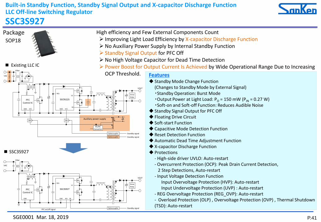
■ Existing LLC IC
■ SSC3S931
LLC Off-line Switching Regulator
P.36 SGE0001 Mar. 18, 2019
Pin Assignment No. Symbol Functions No. Symbol Functions
1 VSEN Mains input voltage detection signal input 10 GND Ground
2 VCC Supply voltage input for the IC with VCC pin overvoltage protection (VCC_OVP) 11 VGL Low-side gate drive output
3 FB Feedback signal input for constant voltage control and optocoupler open protection (OOP) signal input 12 REG Supply voltage output for gate drive circuit
4 DTS Dead time control selection: a fixed on the minimum value, or an automatically adjustment 13 — (Pin removed)
5 CSS Soft-start setting capacitor connection 14 VB Supply voltage input for high-side driver with UVLO
6 CL Overload detection (OLP) capacitor connection 15 VS Floating ground for high-side driver
7 RC Resonant current detection signal input and overcurrent protection (OCP) signal input 16 VGH High-side gate drive output
8 CD Delay time setting capacitor connection for optocoupler open protection (OOP) 17 — (Pin removed)
9 NC Not connected 18 NC Not connected
Parameter Value
VCC Pin Maximum Ratings 35 V
VCC(ON) 11.9 V (typ.)
VCC(OFF) 10.0 V (typ.)
Minimum Oscillation Frequency 31.5 kHz (typ.)
Maximum Oscillation Frequency 300 kHz (typ.)
Maximum Source Current -540 mA (typ.)
Maximum Sink Current 1.50 A (typ.)
VREG 10.0 V (typ.)
Electrical Characteristics Typical Application Circuit
Built-in Standby Function, Standby Signal Output and X-capacitor Discharge Function LLC Off-line Switching Regulator SSC3S931
P.37 SGE0001 Mar. 18, 2019
VAC
VOUT
Error Amp.
SSC9522S
GND
REGVS
RV
PFCControl IC
Auxiliary power supply
Standby signal
SWSW
AC/DC Converter
Optocoupler
Optocoupler Standby signal
VCCGND VCC
VAC
VOUT
Error Amp.
SSC3S900
GND
REGVS
Standby signal Optocoupler
SB
Package SOP18
High efficiency and Few External Components Count
No Auxiliary Power Supply by Internal Standby Function
80 VAC to 265 VAC Input without PFC Circuit < 75 W
No High Voltage Capacitor for Dead Time Detection
Features Standby Mode Change Function
(Changes to Standby Mode by External Signal) ・Standby Operation: Burst Mode ・Output Power at Light Load: PO = 100 mW (PIN = 0.27 W) ・Soft-on and Soft-off Function: Reduces Audible Noise
Floating Drive Circuit Soft-start Function Capacitive Mode Detection Function Reset Detection Function Automatic Dead Time Adjustment Function Brown-in and Brown-out Function Input Electrolytic Capacitor Discharge Function Protections
- High-side driver UVLO: Auto-restart - Overcurrent Protection (OCP): Peak Drain Current Detection, 2 Step Detections, Auto-restart - Overload Protection (OLP) with Input Compensation : Latched Shutdown or Auto-restart - Overvoltage Protection (OVP): Auto-restart - Thermal Shutdown (TSD): Latched Shutdown or Auto-restart
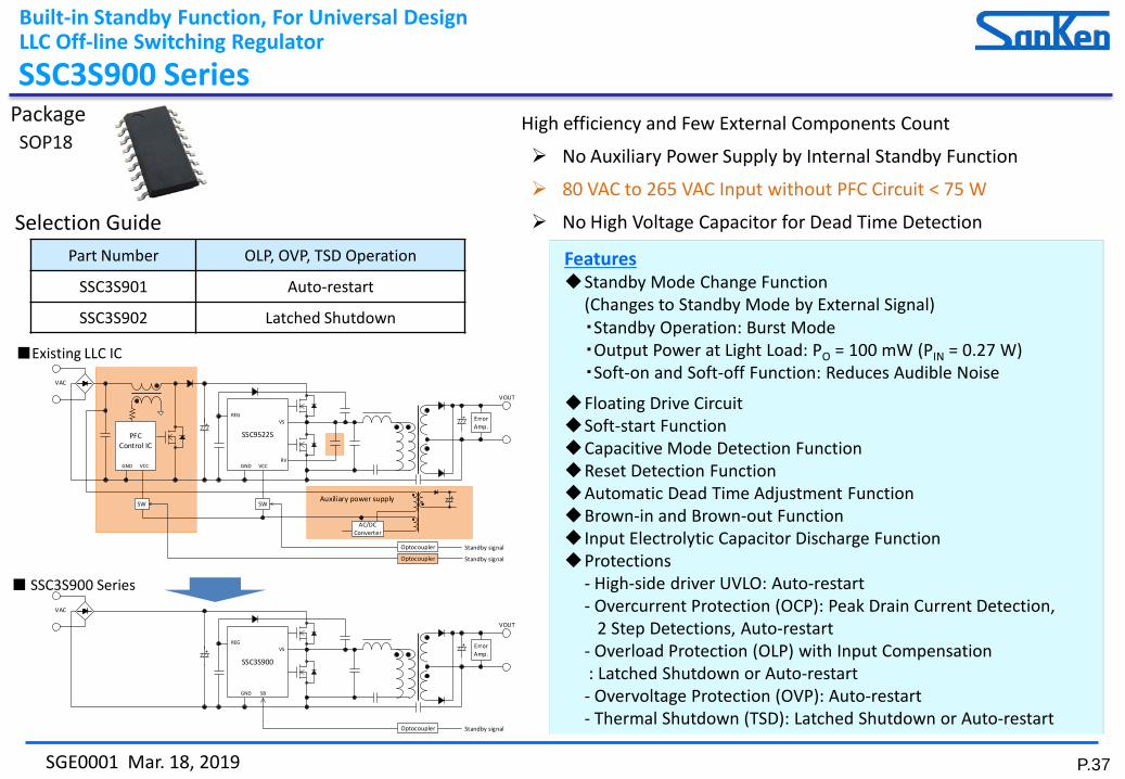
■ SSC3S900 Series
■Existing LLC IC
Built-in Standby Function, For Universal Design LLC Off-line Switching Regulator
Part Number OLP, OVP, TSD Operation
SSC3S901 Auto-restart
SSC3S902 Latched Shutdown
Selection Guide
SSC3S900 Series
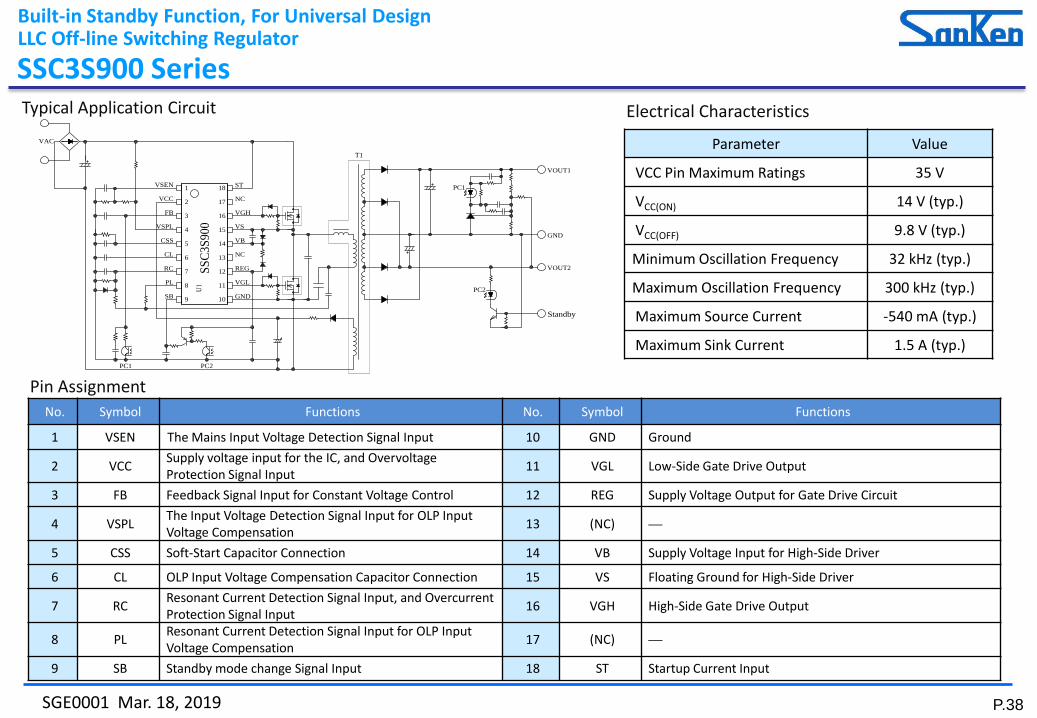
P.38 SGE0001 Mar. 18, 2019
VAC
VSPL
VSEN
VCC
FB
ST
NC
VGH
VS
VB
NC
REG
CSS
CL
PL VGL
GND
RC
SB
Standby
VOUT2
GND
VOUT1
T1
PC1 PC2
PC1
PC2
1
15
16
17
18
4
3
2U
1SS
C3S9
00
7
6
5
12
13
14
9
8
10
11
Pin Assignment No. Symbol Functions No. Symbol Functions
1 VSEN The Mains Input Voltage Detection Signal Input 10 GND Ground
2 VCC Supply voltage input for the IC, and Overvoltage Protection Signal Input 11 VGL Low-Side Gate Drive Output
3 FB Feedback Signal Input for Constant Voltage Control 12 REG Supply Voltage Output for Gate Drive Circuit
4 VSPL The Input Voltage Detection Signal Input for OLP Input Voltage Compensation 13 (NC) —
5 CSS Soft-Start Capacitor Connection 14 VB Supply Voltage Input for High-Side Driver
6 CL OLP Input Voltage Compensation Capacitor Connection 15 VS Floating Ground for High-Side Driver
7 RC Resonant Current Detection Signal Input, and Overcurrent Protection Signal Input 16 VGH High-Side Gate Drive Output
8 PL Resonant Current Detection Signal Input for OLP Input Voltage Compensation 17 (NC) —
9 SB Standby mode change Signal Input 18 ST Startup Current Input
Built-in Standby Function, For Universal Design LLC Off-line Switching Regulator
Parameter Value
VCC Pin Maximum Ratings 35 V
VCC(ON) 14 V (typ.)
VCC(OFF) 9.8 V (typ.)
Minimum Oscillation Frequency 32 kHz (typ.)
Maximum Oscillation Frequency 300 kHz (typ.)
Maximum Source Current -540 mA (typ.)
Maximum Sink Current 1.5 A (typ.)
Electrical Characteristics Typical Application Circuit
SSC3S900 Series
P.39 SGE0001 Mar. 18, 2019
Package SOP18 High efficiency and Few External Components Count
No Auxiliary Power Supply by Internal Standby Function Standby Signal Output for PFC Off No High Voltage Capacitor for Dead Time Detection
Features Standby Mode Change Function
(Changes to Standby Mode by External Signal) ・Standby Operation: Burst Mode ・Output Power at Light Load: PO = 125 mW (PIN = 0.27 W) ・Soft-on and Soft-off Function: Reduces Audible Noise Standby Signal Output for PFC Off Floating Drive Circuit Soft-start Function Capacitive Mode Detection Function Reset Detection Function Automatic Dead Time Adjustment Function Brown-in and Brown-out Function Input Electrolytic Capacitor Discharge Function Protections
- High-side driver UVLO: Auto-restart - Overcurrent Protection (OCP): Peak Drain Current Detection, 2 Step Detections, Auto-restart - Overload Protection (OLP) : Auto-restart - Overvoltage Protection (OVP): Auto-restart - Thermal Shutdown (TSD): Auto-restart
■ Existing LLC IC
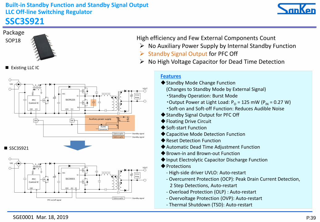
Built-in Standby Function and Standby Signal Output LLC Off-line Switching Regulator
■ SSC3S921
SSC3S921
VAC
VOUT
Error Amp.
SSC9522S
GND
REGVS
RV
PFCControl IC
Auxiliary power supply
Standby signal
SWSW
AC/DC Converter
Optocoupler
Optocoupler Standby signal
VCCGND VCC
VAC
VOUT
Error Amp.
SSC3S921
GND
REGVS
PFCControl IC
Standby signal OptocouplerPFC on/off signal
SBGND ADJ
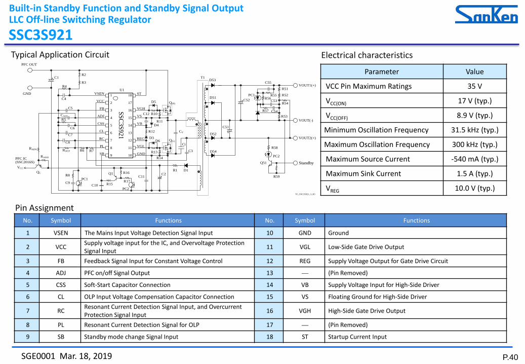
P.40 SGE0001 Mar. 18, 2019
Pin Assignment No. Symbol Functions No. Symbol Functions
1 VSEN The Mains Input Voltage Detection Signal Input 10 GND Ground
2 VCC Supply voltage input for the IC, and Overvoltage Protection Signal Input 11 VGL Low-Side Gate Drive Output
3 FB Feedback Signal Input for Constant Voltage Control 12 REG Supply Voltage Output for Gate Drive Circuit
4 ADJ PFC on/off Signal Output 13 — (Pin Removed)
5 CSS Soft-Start Capacitor Connection 14 VB Supply Voltage Input for High-Side Driver
6 CL OLP Input Voltage Compensation Capacitor Connection 15 VS Floating Ground for High-Side Driver
7 RC Resonant Current Detection Signal Input, and Overcurrent Protection Signal Input 16 VGH High-Side Gate Drive Output
8 PL Resonant Current Detection Signal for OLP 17 — (Pin Removed)
9 SB Standby mode change Signal Input 18 ST Startup Current Input
Parameter Value
VCC Pin Maximum Ratings 35 V
VCC(ON) 17 V (typ.)
VCC(OFF) 8.9 V (typ.)
Minimum Oscillation Frequency 31.5 kHz (typ.)
Maximum Oscillation Frequency 300 kHz (typ.)
Maximum Source Current -540 mA (typ.)
Maximum Sink Current 1.5 A (typ.)
VREG 10.0 V (typ.)
Electrical characteristics Typical Application Circuit
Built-in Standby Function and Standby Signal Output LLC Off-line Switching Regulator
ADJ
VSEN
VCC
FB
ST
VGH
VS
VB
REG
CSS
CL
PL VGL
GND
RC
SB
Standby
VOUT2(+)
VOUT(-)
VOUT1(+)
T1
PC1
PC2
PC1
PC2
1
15
16
17
18
4
3
2
U1
SSC3S921
7
6
5
12
13
14
9
8
10
11
C1R2
R3R4
C4
C5
R5
C7
C8
ROCP R6 R7
R8R1
R10
R11
R12
R13
R14
R15
R16
R17
Q1
Q(H)
Q(L)
C2
C3
C9C10
C11
C12
D1
D3
D4
D5
D6Ci
CV
D51
D52
D53
D54
C51
C52 C53
C54
C55
R51
R52
R53
R54R56
R55
R57
R58
R59
Q51
C6
TC_SSC3S921_3_R3
PFC OUT
PFC IC (SSC2016S)VCC
GND
QC
RADJ1
RADJ2
CADJ
SSC3S921
P.41 SGE0001 Mar. 18, 2019
VOUT
Error Amp.
SSC9522S
GND
REGVS
RV
PFCControl IC
Auxiliary power supply
Standby signal
SWSW
AC/DC Converter
Optocoupler
Optocoupler Standby signal
VCCGND VCC
VAC
Filter
VOUT
Error Amp.
SSC3S927
GND
REGVS
PFCControl IC
Standby signal Optocoupler
SBGND
VAC
Filter
ADJ
PFC on/off signal
Package SOP18
Features Standby Mode Change Function
(Changes to Standby Mode by External Signal) ・Standby Operation: Burst Mode ・Output Power at Light Load: PO = 150 mW (PIN = 0.27 W) ・Soft-on and Soft-off Function: Reduces Audible Noise Standby Signal Output for PFC Off Floating Drive Circuit Soft-start Function Capacitive Mode Detection Function Reset Detection Function Automatic Dead Time Adjustment Function X-capacitor Discharge Function Protections
- High-side driver UVLO: Auto-restart - Overcurrent Protection (OCP): Peak Drain Current Detection, 2 Step Detections, Auto-restart - Input Voltage Detection Function Input Overvoltage Protection (HVP): Auto-restart Input Undervoltage Protection (UVP) : Auto-restart - REG Overvoltage Protection (REG_OVP): Auto-restart - Overload Protection (OLP) , Overvoltage Protection (OVP) , Thermal Shutdown (TSD): Auto-restart
■ Existing LLC IC
Built-in Standby Function, Standby Signal Output and X-capacitor Discharge Function LLC Off-line Switching Regulator
■ SSC3S927
SSC3S927 High efficiency and Few External Components Count Improving Light Load Efficiency by X-capacitor Discharge Function No Auxiliary Power Supply by Internal Standby Function Standby Signal Output for PFC Off No High Voltage Capacitor for Dead Time Detection Power Boost for Output Current Is Achieved by Wide Operational Range Due to Increasing
OCP Threshold.
P.42 SGE0001 Mar. 18, 2019
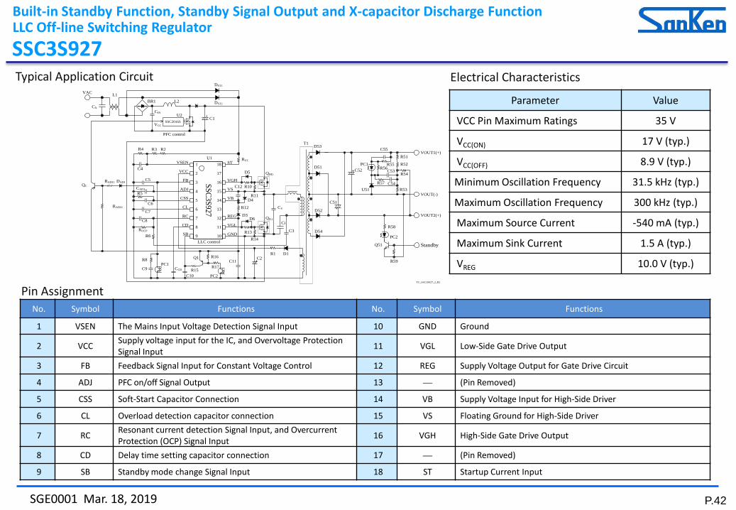
Pin Assignment No. Symbol Functions No. Symbol Functions
1 VSEN The Mains Input Voltage Detection Signal Input 10 GND Ground
2 VCC Supply voltage input for the IC, and Overvoltage Protection Signal Input 11 VGL Low-Side Gate Drive Output
3 FB Feedback Signal Input for Constant Voltage Control 12 REG Supply Voltage Output for Gate Drive Circuit
4 ADJ PFC on/off Signal Output 13 — (Pin Removed)
5 CSS Soft-Start Capacitor Connection 14 VB Supply Voltage Input for High-Side Driver
6 CL Overload detection capacitor connection 15 VS Floating Ground for High-Side Driver
7 RC Resonant current detection Signal Input, and Overcurrent Protection (OCP) Signal Input 16 VGH High-Side Gate Drive Output
8 CD Delay time setting capacitor connection 17 — (Pin Removed)
9 SB Standby mode change Signal Input 18 ST Startup Current Input
Parameter Value
VCC Pin Maximum Ratings 35 V
VCC(ON) 17 V (typ.)
VCC(OFF) 8.9 V (typ.)
Minimum Oscillation Frequency 31.5 kHz (typ.)
Maximum Oscillation Frequency 300 kHz (typ.)
Maximum Source Current -540 mA (typ.)
Maximum Sink Current 1.5 A (typ.)
VREG 10.0 V (typ.)
Electrical Characteristics Typical Application Circuit
Built-in Standby Function, Standby Signal Output and X-capacitor Discharge Function LLC Off-line Switching Regulator SSC3S927
ADJ
VSEN
VCC
FB
ST
VGH
VS
VB
REG
CSS
CL
CD VGL
GND
RC
SB
Standby
VOUT2(+)
VOUT(-)
VOUT1(+)
T1
PC1
PC2
PC1
PC2
1
15
16
17
18
4
3
2
U1
SSC3S927
7
6
5
12
13
14
9
8
10
11
C1
R2R3R4
C4
C5
R5
C7
C8
ROCP
R6
R8R1
R10
R11
R12
R13
R14
R15
R16
R17
Q1
Q(H)
Q(L)
C2
C3
C9
C10
C11
C12
D1
D3
D4
D5
D6Ci
CV
D51
D52
D53
D54
C51
C52 C53
C54
C55
R51
R52
R53
R54R56
R55
R57
R58
R59
Q51
C6
TC_SSC3S927_2_R2
VCC
QCRADJ1
RADJ2
CADJ
RST
CCD
VAC
DST1
CX
L1
DST2
SSC2016S
U2
PFC control
LLC control
U51
L2BR1
CIN
DADJ
P.43 SGE0001 Mar. 18, 2019
REG12
SSC3S921/27
ADJ
GND
PFC IC(SSC2016S)
VCC
GND
4
10
REG12
SSC3S921/27
ADJ
GND
PFC IC
VCC
GND
4
10
2 VCC
D
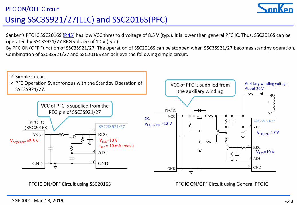
PFC ON/OFF Circuit
Sanken’s PFC IC SSC2016S (P.45) has low VCC threshold voltage of 8.5 V (typ.). It is lower than general PFC IC. Thus, SSC2016S can be operated by SSC3S921/27 REG voltage of 10 V (typ.). By PFC ON/OFF Function of SSC3S921/27, The operation of SSC2016S can be stopped when SSC3S921/27 becomes standby operation. Combination of SSC3S921/27 and SSC2016S can achieve the following simple circuit.
ex. VCC(ON)PFC =12 V
VREG=10 V
VCC(ON)=17 V
Auxiliary winding voltage, About 20 V
VREG=10 V IREG=-10 mA (max.)
VCC(ON)PFC =8.5 V
PFC IC ON/OFF Circuit using General PFC IC PFC IC ON/OFF Circuit using SSC2016S
VCC of PFC is supplied from the auxiliary winding
VCC of PFC is supplied from the REG pin of SSC3S921/27
Simple Circuit. PFC Operation Synchronous with the Standby Operation of
SSC3S921/27.
Using SSC3S921/27(LLC) and SSC2016S(PFC)
P.44 SGE0001 Mar. 18, 2019
VAC
VPFCOUT
GND
PFCControl IC
Rectification Diode
Bypass Diode
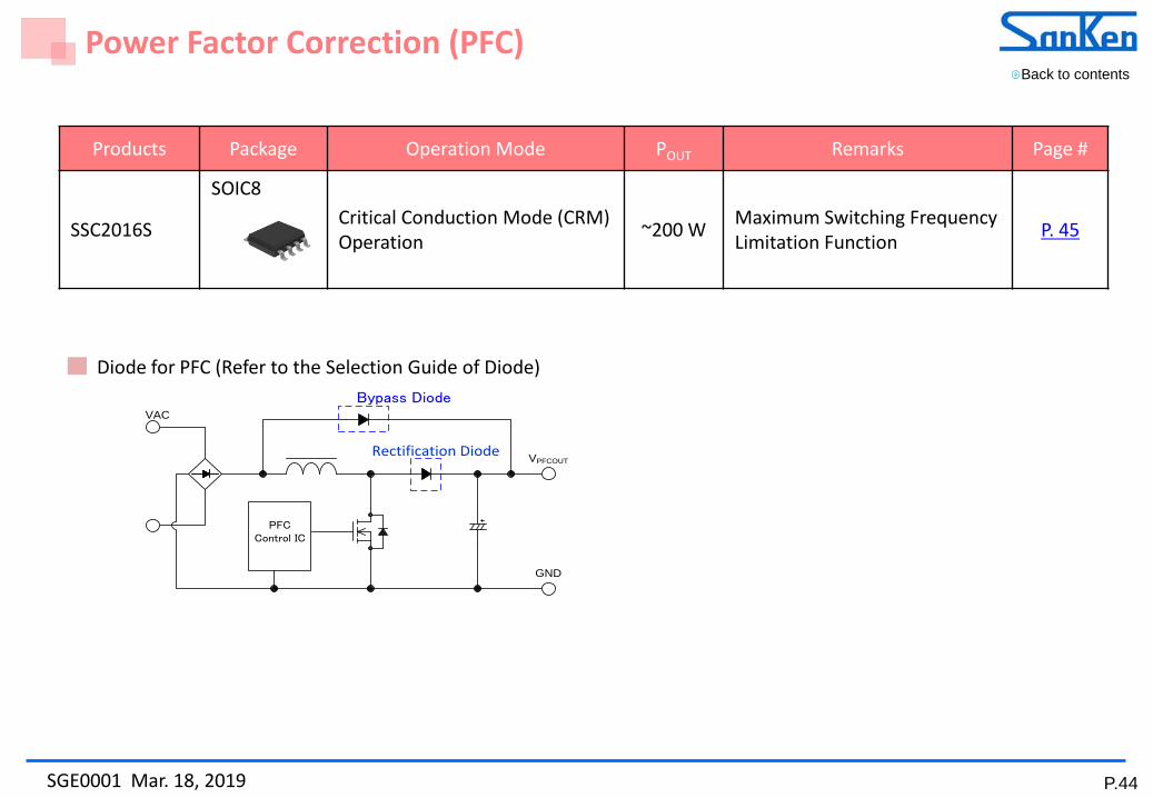
Products Package Operation Mode POUT Remarks Page #
SSC2016S
SOIC8 Critical Conduction Mode (CRM) Operation ~200 W Maximum Switching Frequency
Limitation Function P. 45
Back to contents
Diode for PFC (Refer to the Selection Guide of Diode)
Power Factor Correction (PFC)
P.45 SGE0001 Mar. 18, 2019
Power Factor Correction (PFC) IC of CRM Operation
Part Number VCC(ON) VFB(REF)
IOUT
Source IOUT
Sink
SSC2016S 8.5 V 2.50 V −500 mA 1000 mA
Critical Conduction Mode (CRM) For PFC Circuit up to 200 W of Output Power Light Load Efficiency Is Improved by Maximum Switching
Frequency Limitation Function Low Standby Power
(No Input Voltage Sensing Resistors Required)
Features Critical Conduction Mode (CRM) Low Standby Power (No Input Voltage Sensing Resistors Required) Maximum Switching Frequency Limitation Function Maximum on-Time Limiting Function Restart Function
Protections - Overcurrent Protection 1(OCP1): Pulse-by-Pulse - Overcurrent Protection 2(OCP2): Latched Shutdown - Overvoltage Protection (OVP): Auto-restart - FB Pin Undervoltage Protection (FB_UVP): Auto-restart - Thermal Shutdown (TSD): Auto-restart
Pin No. Symbol Functions
1 FB Feedback, OVP and UVLO Signal Input
2 CT Timing capacitor connection
3 COMP Phase compensation
4 CS Overcurrent protection Signal Input
5 ZCD ZCD Signal Input and delay time adjustment
6 GND Ground
7 OUT Gate drive output
8 VCC Power supply input for control circuit
Pin Assignment Circuit
Package SOIC8
VAC
C1
BR1P
C2
RVS2
VOUT
VCC
OUT CT
NC
FB
CS
GND
ZCD
8
7
6
5
SSC2016S
U1
1
2
4
3COMPCSRS
C7
External power supply
R5
C4
C5
C6
C3
Q1
DFW
DBYP
R2
R3 R4
LINE GND
RVS1
RCS
D
D1T1
R1
TC_SSC2016S_1_R2
CP
SSC2016S
P.46 SGE0001 Mar. 18, 2019
Important Notes
All data, illustrations, graphs, tables and any other information included in this document (the “Information”) as to Sanken’s products listed herein (the “Sanken Products”) are current as of the date this document is issued. The Information is subject to any change without notice due to improvement of the Sanken Products, etc. Please make sure to confirm with a Sanken sales representative that the contents set forth in this document reflect the latest revisions before use. The Sanken Products are intended for use as components of general purpose electronic
equipment or apparatus (such as home appliances, office equipment, telecommunication equipment, measuring equipment, etc.). Prior to use of the Sanken Products, please put your signature, or affix your name and seal, on the specification documents of the Sanken Products and return them to Sanken. When considering use of the Sanken Products for any applications that require higher reliability (such as transportation equipment and its control systems, traffic signal control systems or equipment, disaster/crime alarm systems, various safety devices, etc.), you must contact a Sanken sales representative to discuss the suitability of such use and put your signature, or affix your name and seal, on the specification documents of the Sanken Products and return them to Sanken, prior to the use of the Sanken Products. The Sanken Products are not intended for use in any applications that require extremely high reliability such as: aerospace equipment; nuclear power control systems; and medical equipment or systems, whose failure or malfunction may result in death or serious injury to people, i.e., medical devices in Class III or a higher class as defined by relevant laws of Japan (collectively, the “Specific Applications”). Sanken assumes no liability or responsibility whatsoever for any and all damages and losses that may be suffered by you, users or any third party, resulting from the use of the Sanken Products in the Specific Applications or in manner not in compliance with the instructions set forth herein. In the event of using the Sanken Products by either (i) combining other products or materials or
both therewith or (ii) physically, chemically or otherwise processing or treating or both the same, you must duly consider all possible risks that may result from all such uses in advance and proceed therewith at your own responsibility. Although Sanken is making efforts to enhance the quality and reliability of its products, it is
impossible to completely avoid the occurrence of any failure or defect or both in semiconductor products at a certain rate. You must take, at your own responsibility, preventative measures including using a sufficient safety design and confirming safety of any equipment or systems in/for which the Sanken Products are used, upon due consideration of a failure occurrence rate and derating, etc., in order not to cause any human injury or death, fire accident or social harm which may result from any failure or malfunction of the Sanken Products. Please refer to the relevant specification documents and Sanken’s official website in relation to derating. No anti-radioactive ray design has been adopted for the Sanken Products. The circuit constant, operation examples, circuit examples, pattern layout examples, design
examples, recommended examples, all information and evaluation results based thereon, etc., described in this document are presented for the sole purpose of reference of use of the Sanken Products.
Sanken assumes no responsibility whatsoever for any and all damages and losses that may be suffered by you, users or any third party, or any possible infringement of any and all property rights including intellectual property rights and any other rights of you, users or any third party, resulting from the Information. No information in this document can be transcribed or copied or both without Sanken’s prior
written consent. Regarding the Information, no license, express, implied or otherwise, is granted hereby under
any intellectual property rights and any other rights of Sanken. Unless otherwise agreed in writing between Sanken and you, Sanken makes no warranty of any
kind, whether express or implied, including, without limitation, any warranty (i) as to the quality or performance of the Sanken Products (such as implied warranty of merchantability, and implied warranty of fitness for a particular purpose or special environment), (ii) that any Sanken Product is delivered free of claims of third parties by way of infringement or the like, (iii) that may arise from course of performance, course of dealing or usage of trade, and (iv) as to the Information (including its accuracy, usefulness, and reliability). In the event of using the Sanken Products, you must use the same after carefully examining all
applicable environmental laws and regulations that regulate the inclusion or use or both of any particular controlled substances, including, but not limited to, the EU RoHS Directive, so as to be in strict compliance with such applicable laws and regulations. You must not use the Sanken Products or the Information for the purpose of any military
applications or use, including but not limited to the development of weapons of mass destruction. In the event of exporting the Sanken Products or the Information, or providing them for non-residents, you must comply with all applicable export control laws and regulations in each country including the U.S. Export Administration Regulations (EAR) and the Foreign Exchange and Foreign Trade Act of Japan, and follow the procedures required by such applicable laws and regulations. Sanken assumes no responsibility for any troubles, which may occur during the transportation of
the Sanken Products including the falling thereof, out of Sanken’s distribution network. Although Sanken has prepared this document with its due care to pursue the accuracy thereof,
Sanken does not warrant that it is error free and Sanken assumes no liability whatsoever for any and all damages and losses which may be suffered by you resulting from any possible errors or omissions in connection with the Information. Please refer to our official website in relation to general instructions and directions for using the
Sanken Products, and refer to the relevant specification documents in relation to particular precautions when using the Sanken Products. All rights and title in and to any specific trademark or tradename belong to Sanken and such
original right holder(s). DSGN-CEZ-16003