ad-i24633 rdinade r)iin oeseatchec ola using a ia i
TRANSCRIPT
AD-i24633 RDINADE R)IIN OESEATCHEC OLA USING A iA i/R~~~D-RODE 6A33() B RESEAGAN RINGOPHTCHEI HLAB USIN G JOSM CA
POKROWdSKY ET AL. 87 FEB 83 TR-5 N8@@14-8i-C-8i65
UNCLASSIFIED F/G 7/5 N
FENDmm LL

1..
S.2.0
t MICROCOPY RESOLUTION TEST CHART ,
ii NATINAL. BUREAU OF STANDARD-1963-A
'.
7" ~~ 3

~.-... .:. .-.... . .. . ---. -., - -.. _ .. . _ . . . . -_ . . . . . . . .. . .......:.-.... .-.* ~fn~iassif led a..
SECURITY CLASSIFICATION OF THIS PAGE ("mn Data Entero*
REPORT DOCUMENTATION PAGE READ INSTRUCTIONSBEFORE COMPLETING FORM1. REPORT NUMBER 12. GOVT ACCESSION NO. 3. RECIPIENT'S CATALOG NUMBER
4. TITLE (and Subitl.) S. TYPE Of REPORT & PERIOD COVERED
Reading and Writing of Photochemical HolesUsing GaAlAs Diode Lasers Technical Report
6. PERFORMING ORO. REPORT NUMBER
* 7. AUTHOR(a) S. CONTRACT OR GRANT NUMBER(@)
P. Pokrowsky, W. E. Moerner, F. Chu,G. C. Bjorklund N00014-81-C-0165
S. PERFORMING ORGANIZATION NAME AND ADDRESS 10. PROGRAM ELEMENT. PROJECT. TASK
International Business Machines, Dept. K46 AREA A WORK UNIT NUMBERS
5600 Cottle RoadSan Jose, California NR 421-001
11. CONTROLLING OFFICE NAME AND ADDRESS 12. REPORT OATS
Office of Naval Research I 19"800 N. Quincy Street C 2. NUMUErOPPAGtS 7
Arlington, VA 22217 Code 24014. MONITORING AGENCY NAME & ADORESS(If dillfrent fom Contirollig Office) IS. SECURITY CLASS. (of this report)
UnclassifiedOS. OECL ASSI PI CATION/OOWNGRADINGSCHEDULE
IS. OISTRIBUTION STATEMENT (of thl Report)
This document has been approved for public release and sale;its distribution is unlimited. DTICE""
17. DISTRIBUTION STATEMENT (of the abstract entered In Block 20, If dilfllet from Reol)
"-.FEB 1 8 1983
Il. SUPPLEMENTARY NOTES
Submitted to Optics Letters
19. KEY WORDS (Continue on rever@e aide It nocoeeoay &d identify by block number)
Optical storage, optical memories, cryogenics, tunable lasers, diodelasers, photochemistry
20. ABSTRACT (Cantlnn. i rov aie I nee**Oa aid Identify by block numbe)
0...A current tuned Ga*l.As diode laser is utilized both to burn and to detect
narrow photochemicalholes in the inhomogeneously broadened 833 ram zerophonon line of the RI color center in LIF. Applications for reading and
" U writing data into frequency domain optical memories based on photochemical. _hole burning are discussed.
DD I5=16 1473 EDITION OI Novis OSSOE UnclassifiedS/N 0102- LF-014- 6601 SECURITY CLASSIFICATION OF THIS PAGE (Whim Dole an ereo
a AL
".5
• -.°- ./.: -.- ,, - ..-+:. : : .I< -" - - ' - : "- - " i . - =, d . i ' - " '' ""
OFFICE OF NAVAL RESEARCH
Contract N00014-81 -C-0165
Task No. NR 421-001
TECHNICAL REPORT NO. 5
Reading and Writing of Photochemical Holes Using
GaAIAs Diode Lasers
by
P. Pokrowsky, W. E. Moerner, F. Chu, and G. C. Bjorklund
Prepared for PublicationL~cio o!ZTTS GRA&I
in L''CT1IT-i'inuiied E
* Optics Letters JU r. t ificat jo
SBy -
Avx.X l' Codes
IBM Research Laboratory A.San Jose, California 95193
February 7, 1983A
Reproduction In whole or in part is permitted for aany purpose of the United States Government
This document has been approved for public releaseand sale; its distribution Is unlimited

READING AND WRITING OF PHOTOCHEMICAL HOLES
P. Pokrowsky*W. E. Moerner
F. Chui:".:Z ' .G. C. Bjorklund
i-: IBM Research Laboratory~San Jose, California 95193
ABSTRACT: A current tuned GaAIAs diode laser is utilized both to burn and to detect
narrow photochemical holes in the inhomogeneously broadened 833 nm zero phonon line of
the R' color center in LiF. Applications for reading and writing data into frequency domain
optical memories based on photochemical hole burning are discussed.
*On leave from GKSS-Forschungszentrum Geesthacht, West Germany.
b-a
,,
-. . . . . . . .
.. . . . . . . . . . . . .

"- 1
There has recently been considerable interest in the cryogenic phenomenon of
photochemical hole burning1 both as a tool for high resolution solid state spectroscopy2 ,3
and as a means for frequency domain optical storage. 4 ,5 This phenomenon occurs whenever
persistent photochemical changes can be induced by exposure to narrow band optical
radiation tuned to a frequency within the inhomogeneously broadened zero phonon line of a
photoactive material contained in a crystalline or an amorphous host. The narrow band
radiation selectively excites that fraction of the molecules of photoactive material whose local
environment is such that their resonant absorption frequency is within a homogeneous
linewidth of the excitation frequency. The ensuing photochemical reaction alters the excited
molecules so that they no longer contribute to absorption at the laser wavelength, resulting in
a persistent narrow hole or dip in the fineshape. Typical ratios of inhomogeneous to
homogeneous widths are on the order of 103 . Thus, 103 resolvable holes can be burned into
the inhomogeneous line at each spatial location in the sample. If one bit of information is
encoded by the presence or absence of a hole at a given location in frequency space and if
the exciting laser is focused to a diffraction limited spot 1 ism in diameter, spatial storage
densities of 103 bits/.um2 or 1011 bits/cm2 might ultimately be possible.
In this paper, we report the first demonstration of photochemical hole burning using
*. GaAIAs diode lasers. These lasers have many advantageous properties for optical storage
" applications. They are compact, reliable, have modest power requirements, operate in a single
* longitudinal and transverse mode with no external cavity, and can be rapidly tuned by
varying the injection current. 6 In our experiments, a current-tuned commercially available
S'.GaAIAs diode laser was utilized both to burn (write) and detect (read) persistent narrow
photochemical holes in the 0.4 nm wide inhomogeneously broadened 833.0 nm zero phonon
line of the R' aggregate color center contained in Mg++ doped LiF. Exposures on the order
o-A
-a -- .. . . . . ..- - - - -. . . . . .- . - - . . , l
* 2
of several J/cm2 were sufficient to write 500 MHz (0.001 nm) wide holes with a depth
equal to approximately 5% of the inhomogeneous lineshape.
The R' in LiF:Mg + + system was chosen because photochemical hole burning in this
system has recently been demonstrated using actively stabilized IR dye lasers.7 The
R' center is not actually a molecule, but rather is a negatively charged intrinsic aggregate
color center consisting of 3 trigonally-arranged anion vacancies surrounded by 4 trapped
electrons. The center is produced in LiF:Mg++ by x-ray irradiation at room temperature. 8
Doping with Mg++ ions in the melt has been shown to enhance the achievable R'
population.9 When cooled to liquid He temperatures, irradiated crystals exhibit a prominent
zero phonon line centered at 833.0 nm. The photochemical mechanism responsible for the
hole burning is conjectured to be ionization caused by electron.tunneling from photoexcited
centers to nearby traps.3,7 Preliminary materials studies7 suggest that the hole-burning
mechanism may also involve a weak photophysical component.
The sample used in our experiments consisted of a 0.6 cm x 0.5 cm x 0.3 cm thick
crystal of LiF doped with 0.05 mole % MgF 2 and exposed to Cu x-rays for 100 hours at
room temperature. Immediately after x-ray irradiation, the sample was cooled to 2K, and the
833 nm zero phonon line observed in absorption using white light illumination and a
spectrometer. The peak absorption at the linecenter was 30% for a 0.3 cm pathlength and
the observed inhomogeneous linewidth was 0.4 nm (full width at half-maximum absorption).
The setup for the GaAIAs diode laser hole burning experiments is shown in Figure 1.
A single Mitsubishi 3001 TIS GaAIAs diode laser was utilized in all of the experiments. The
. laser output beam was collimated by a microscope objective and then focused onto the
crystal sample which was fixed on a mount contained in a liquid He immersion dewar at 20K.

3
Pinholes of various diameters between 50 and 500 ;m were mounted directly in front of the
crystal to produce a controlled spot size. Intensity and exposure times were adjusted by a
shutter and attenuators before the dewar. The power of the transmitted beam was monitored
with a fast PIN photodiode (Motorola type MRD5 10).
Coarse wavelength tuning was provided by temperature tuning. The GaAlAs diode was
mounted on a Peltier Cooler which could be adjusted between 00 and 50 C with a stability
of 0.05*C. Fine tuning was provided by varying the injection current using specially built
electronics. For writing holes, the injection current was stabilized to ±0.02 mA, resulting in
a measured laser emission jitter bandwidth of 200 MHz. For reading holes, the injection
current was periodically linearly ramped in a sawtooth manner and at the same time rapidly
modulated with a low amplitude, sinusoidal waveform. The ramping caused the laser
frequency to repetitively scan over the spectral region containing the hole, while the
..- sinusoidal modulation caused a rapid dithering of the laser frequency for derivative
spectroscopy.
The ramping rate was varied from less than 1 Hz to over 20 kHz. Under these
conditions, such lasers can be smoothly tuned over impressive ranges. In fact, 60 GHz of
tuning without a mode hop has been achieved with slow ramping and 40 GHz of tuning has
been achieved at 25 kHz ramping rates.1 0 The sinusoidal modulation was performed at a
frequency of 2.5 kHz for the slow ramping experiments and at frequencies above 10 MHz for
the fast ramping experiments. Derivative *spectroscopy of the holes was performed by
Smonitoring the transmitted laser power and detecting the amplitude of the Fourier component
of the signal at the sinusoidal modulation frequency. For slow ramping, the 2.5 kHz signals
were detected using a lock-in amplifier and displayed on an x-y recorder. For fast ramping,
the high frequency signals were homodyne detected using a Mini-Circuits type ZFM-4 double
4
balanced mixer and an oscilloscope for display. 10 In both cases, the displayed signals should
show the derivative of the absorptive profile, however, at fast ramping speeds the derivative
lineshapes were distorted due to the limited 1 MHz bandwidth of the oscilloscope amplifier
(Tektronix 7A22 Differential Amplifier).
The best signal to noise was obtained at slow ramping rates. Since the bandwidth of
the detection electronics could be narrowed to less than 100 Hz, the optical detection system
was very sensitive. All of the slow ramping experiments were done with the laser power
attenuated to I pW or less. This prevented deleterious additional hole burning while reading
and allowed holes to last for several hours under conditions of continuous repetitive reading.
Figure 2 shows typical derivative spectra taken before burning a hole (upper trace), after
burning one hole (middlq trace), and after burning one additional hole (bottom trace). All
-three traces were taken at one spot on the sample. For each trace, the laser injection current
was slowly ramped between 19.6 and 20.6 mA, resulting in a 9 GHz optical frequency scan.
The focused spot size on the sample was 0.002 cm2 . The holes were burned by stabilizing
the injection current to a constant value, turning off the sinusoidal modulation, and removing
the attenuators to expose the sample to 2 mW of laser power for 15 seconds.
The derivative spectra of the holes is somewhat more complicated than would have
been expected for a simple Lorentzian UIneshape, since each hole appears to be accompanied
by several weaker "sideholes." (Similar sideholes were observed in the JR dye laser
experiments of Reference 7.) The predominant central feature is always centered at the
burning wavelength. Neglecting the sideholes, an "effective holewidth" can be defined as the
frequency displacement between the extrema of the central feature. In these experiments,
the effective holewidth was 500 MHz (or 0.001 nm). A comparison of the middle and
bottom traces shows that the depth of a previously written hole decreases if a new hole is
.

burned next to it. This "hole interaction" effect is quite reproducible, but does not pose a
3 serious problem for the optical storage application, since the effect becomes much less
significant for widely separated holes.
Optical storage applications require data rates which can only be achieved using fast
ramping. Figure 3 shows signals which were taken before burning a photochemical hole,
after burning one hole and after burning a second hole. (The hole burning conditions were
essentially the same as for Figure 2.) However, in this case, the laser frequency was scanned
over 17 GHz at a 30 kHz rate, corresponding to a slewing rate of 1 GHz/j~sc. The
sinusoidal modulation frequency was 179 MHz and the reading laser power was about
0.5 mW. The signal lineshapes are considerably distorted from the true derivative shape due
to the limited bandwidth of the detection electronics. This, however, is not a disadvantage
for reading data from an optical storage device, since the only relevant information is the
presence or absence of the hole. The fastest detection time we could achieve for these
relatively shallow, 500 MHz wide holes, was 500 nsec. Under these conditions, the hole
could be detected for at least 5 minutes, Corsndg to 10 reads, before deleterious
additional hole burning became significant.
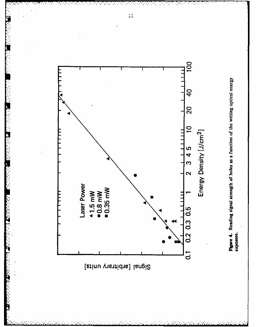
Finally, a series of experiments was conducted to determine the required optical energy
density exposure necessary to burn detectable photochemical holes. The focused spot size
was carefully controlled by placing a thin foil with pinholes of known diameter directly
against the front surface of the crystal. The total laser power incident on the crystal was
determined by measuring the power transmitted by the pinhole, crystal, and dewar and then
correcting for the known values of the crystal loss and dewar window losses. The energy
density exposure was then controlled by varying the exposure time over the range 0.1 to
10 seconds. Figure 4 shows results for an 125 #~m diameter pinhole. There is an

w. . . .. . .. . . .
6
approximately linear relationship between the derivative signal amplitude and the logarithm
of the exposure. It can be seen that very high exposures of several J/cm2 are necessary.
For practical optical storage applications, where detectable holes must be written in 100 nsec
or less with a nominal 3 mW of laser power and nominal spot size of 10-7 cm2 , this
sensitivity would have to be improved by 3 orders of magnitude.
In conclusion, we have demonstrated both writing (burning) and reading (detection) of
narrow photochemical holes using practical, current tuned GaAIAs diode lasers. The
recording material consisted of R' aggregate color centers contained in Mg++ doped LiF.
The effective holewidth was about 500 MHz (0.001 nm), implying that 500 resolvable holes
could be written into the 250 GHz (0.5 nm) wide zero phonon line at 833.0 nm. We are
currently searching for means to enhance the sensitivity of this material to achieve the
writing speeds necessary for optical storage applications.
This work was partially supported by the Office of Naval Research.
"~1.

- . . 7
REFERENCES
1. B. M. Kharlamov, R. I. Personov, and L. A. Bykovskaya, Opt. Comm. 12, 191 (1974);
A. A. Gorokovskii, R. K. Kaarli, and L. A. Rebane, JETP Lett. 20, 216 (1974);
H. de Vries and D. A. Wiersma, Phys. Rev. Lett. 36, 91 (1976).
2. S. Voelker, R. M. Macfarlane, A. Z. Genack, H. P. Trommsdorff, and
J. H. van Der Waals, J. Chem. Phys. 67, 1759 (1977).
3. R. M. Macfarlane and R. M. Shelby, Phys. Rev. Lett. 42, 788 (1979);
M. D. Levenson, R. M. Macfarlane, and R. M. Shelby, Phys. Rev. B22, 4915 (1980).
4. A. Szabo, U.S. Patent No. 3, 896, 420 (1975); G. Castro, D. Haarer,
R. M. Macfarlane, and H. P. Trommsdorff, U.S. Patent No. 4, 101, 976 (1978).
5. D. Haarer, SPIE 177, 97 (1979); C. Ortiz, R. M. Macfarlane, R. M. Shelby,
W. Lenth, and G. C. Bjorklund, Appl. Phys. 25, 87 (1981); W. Lenth, C. Ortiz,
G. C. Bjorklund, Opt. Lett. 6, 351 (1981); G. C. Bjorklund, W. Lenth, and C. Ortiz,
SPIE 298, 107 (1981).
6. H. Kressel and J. K. Butler, Semiconductor Lasers and Heterojunction LEDs
,.:. (Academic Press, 1977).
7. W. E. Moerner, F. M. Schellenberg, and G. C. Bjorklund, Appi. Phys. B28, 268
(1982); W. E. Moerner, P. Pokrowsky, F. M. Schelienberg, and G. C. Bjorklund (to
be published).
8. D. B. Fitchen, H. R. Fetterman, and C. B. Pierce, Solid State Comm. 4, 205 (1966).
9. A. E. Hughes, Solid State Comm. 4, 337 (1966).
10. P. Pokrowsky, W. Zapka, F. Chu, and 0. C. Bjorklund Opt. Comm. (to be published).
-. S4S~........ . ....',°.... o.'.r. ......... ," .. ... ,.... ..... ,...... .. . ..... ........... .... - .

0 4)
II CIACA
041%0
CC*E
CL

(b)
(C)
0 2 4 6 8I, v [GHzJ
19.6 19.8 20.0 20.2 20.4 20.6I (mA]
Figure 2. Reading of holes using derivative spectroscopy and slow ramping: (a) beforewriting a hole, (b) after writing one hole, and (c) after burning a second hole.

=N--
1m 1
F~gue 3. Reading of holes with fast ramping: (a) before writing a hole, (b) after writingone hole, and (c) after writing a second hole.
CV3o
4' A
CV4)ogCN
EC
VIM,
d0
[siun jej~qj] luNO

472-3/A1 472:GAN: 716:enj78u472-608
TECHNICAL REPORT DISTRIBUTION LIST, GEN
NO.* No.Copies Copies
- Office of Naval Research U.S. Army Research OfficeAttn: Code 472 Attn: CRD-AA-IP800 North (aincy Street P.O. Box 1211Arlington, Virginia 22217 2 Research Triangle Park, N.C. 27709
ONR Western Regional Office Naval Ocean Systems Center. Attn: Dr. R. J. Marcus Attn: Mr. Joe McCartney
1030 East Green Street San Diego, California 92152 1Pasadena, California 91106 1
Naval Weapons CenterONR Eastern Regional Office Attn: Dr. A. B. Amster,Attn: Dr. L. H. Pebles Chemistry DivisionBuilding 114, Section D China Lake, California 93555
-: 666 Sumer StreetBoston, Massachusetts 02210 Naval Civil Engineering Laboratory
Attn: Dr. R. W. DriskoDirector, Naval Research Laboratory Port Hueneme, California 93401Attu: Code 6100W Washington, D.C. 20390 1 Department of Physics & Chemistry
Naval Postgraduate Schooli The Assistant Secretary Monterey, California 93940of the Navy (RE&S)
Department of the Navy Scientific Advisor* Room 4E736, Pentagon Commandant of the Marine Corps
Washington, D.C. 20350 1 (Code RD-I)Washington, D.C. 20380
Comander, Naval Air Systems CommandAtta: Code 310C (H. Rosenmasser) Naval Ship Research and DevelopmentDepartment of the Navy CenterWasbingt.oj, D.C. 20360 1 Attn: Dr. G. Bosmajian, Applied
Chemistry DivisionDefense Technical Information Center Annapolis, Maryland 21401Building 5, Cameron StationAlexandria, Virginia 22314 12 Naval Ocean Sysiems Center
Attn: Dr. S. Yamamoto, MarineDr. Fred Saalfeld Sciences DivisionChemistry Division, Code 6100 San Diego, California 91232Naval Research LaboratoryWashington, D.C. 20375 1 ft. John Boyle
Materials BranchNaval Ship Engineering CenterPhiladelphia, Pennsylvania 19112
o.. .J

SP472-3/A3 472: GAN:
* 7&&4 7 2-6 08
TECHICAL REPORT DISTRIBUTION LIST, GEN
Copies
Mr. James ZalleyDTNSRDC Code 2803
* Annapolis, Maryland 21402 1
M r. A. Me An-aloneAdministrative Librarian
* PLA STE C/ARRADCOM.* Bldg 3401* Dover, New Jersey 078011
2

SP482-3/A23 472:GAN:716:ddc
78u 472-608
TECIICAL REPORT DISTRIBUTION LIST, 051A
o. * No.Copies Copies
Dr. M. A. El-Sayed Dr. M. RauhutDepartment of Chemistry Chemical Research DivisionUniversity of California, American Cyanamid Company
Los Angeles Bound Brook, New Jersey 08805Los Angeles, California 90024 1
Dr. J. I. ZinkDr. E. R. Bernstein Department of ChemistryDepartment of'Chemistry University of California,Colorado State University Los AngelesFort Collins, Colorado 80521 Los Angeles, California 90024
Dr. C. A. HellerNaval Weapons CenterCode 6059China Lake, California 93555 1
Dr. J. R. MacDonaldChemistry Division Dr. John CooperNaval Research Laboratory Code 6130Code 6110 Naval Research LaboratoryWashington, D.C. 20375 1 Washington, D.C. 20375
Dr. G. B. Schuster Dr. William M. JacksonChemistry Department Department of ChemistryUniversity of Illinois Howard UniversityUrbana, 1inois 61801 1 Washington, DC 20059
Dr. A. Adamson Dr. George E. WalraffenDepartment of Chemistry Department of ChemistryUniversity of Southern Howard University
California Washington, DC 20059' Los Angeles, California 90007 1
Dr. D. Burland
Dr. M. S. Wrighton IBMDepartment of Chemistry San Jose Research CenterMassachusetts Institute of 5600 Cottle Road
Technology San Jose, California 95143Cambridge, Massachusetts 02139 1
Dr. A. Paul SchaapChemistry DepartmentWayne State UniversityDetroit, Michigan 49202
:..7

TECHNICAL REPORT DISTRIBUTION LIST, 240
NO.Copies
Mr. Phil AndrewsNAVSEA 8802221 Jefferson Davis HighwayArlington, VA 203601
Mr. Romulus FratilloNAVELEX 6132511 Jefferson Davis HighwayArlington, VA 203601
Mr. B. ZempolichNAVAIR 360B1411 Jefferson Davis HighwayArlington, VA 203601
Mr. R. FedorakNaval Air Development CenterWarmuinster, PA 189741

II I