ad9856 cmos 200 mhz quadrature digital … 200 mhz quadrature digital upconverter ... information...
TRANSCRIPT
CMOS 200 MHzQuadrature Digital Upconverter
AD9856
Rev. C Information furnished by Analog Devices is believed to be accurate and reliable. However, no responsibility is assumed by Analog Devices for its use, nor for any infringements of patents or other rights of third parties that may result from its use. Specifications subject to change without notice. No license is granted by implication or otherwise under any patent or patent rights of Analog Devices. Trademarks and registered trademarks are the property of their respective owners.
One Technology Way, P.O. Box 9106, Norwood, MA 02062-9106, U.S.A. Tel: 781.329.4700 www.analog.com Fax: 781.326.8703 © 2005 Analog Devices, Inc. All rights reserved.
FEATURES Universal low cost modulator solution for communications
applications DC to 80 MHz output bandwidth Integrated 12-bit D/A converter Programmable sample rate interpolation filter Programmable reference clock multiplier Internal SIN(x)/x compensation filter >52 dB SFDR @ 40 MHz AOUT
>48 dB SFDR @ 70 MHz AOUT
>80 dB narrow-band SFDR @ 70 MHz AOUT
+3 V single-supply operation Space-saving surface-mount packaging Bidirectional control bus interface Supports burst and continuous Tx modes Single-tone mode for frequency synthesis applications Four programmable, pin-selectable, modulator profiles Direct interface to AD8320/AD8321 PGA cable driver
APPLICATIONS HFC data, telephony, and video modems Wireless and satellite communications Cellular base stations
GENERAL DESCRIPTION
The AD9856 integrates a high speed, direct digital synthesizer (DDS), a high performance, high speed, 12-bit digital-to-analog converter (DAC), clock multiplier circuitry, digital filters, and other DSP functions on a single chip to form a complete quadrature digital upconverter device. The AD9856 is intended to function as a universal I/Q modulator and agile upconverter for communications applications where cost, size, power dissipation, and dynamic performance are critical attributes.
The AD9856 is available in a space-saving surface-mount package, and is specified to operate over the extended industrial temperature range of −40°C to +85°C.
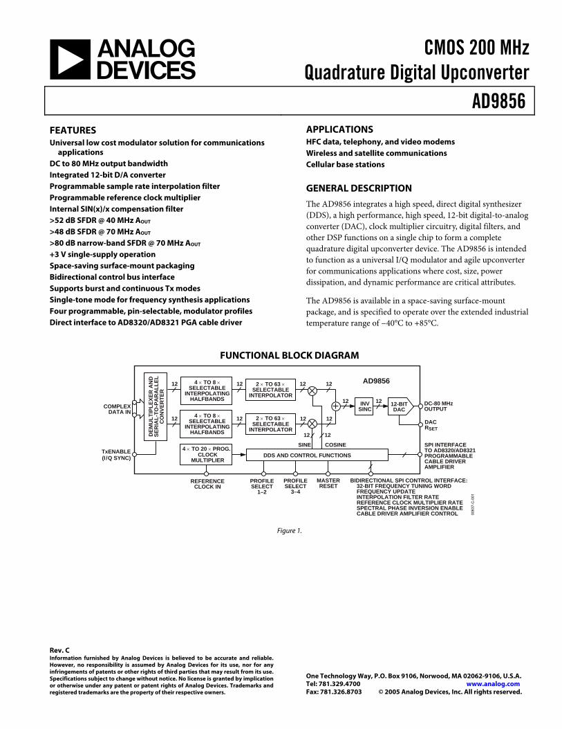
FUNCTIONAL BLOCK DIAGRAM
0063
7-C
-001
12-BITDAC
12
1212
COSINESINE
COMPLEXDATA IN
REFERENCECLOCK IN
TxENABLE(I /Q SYNC)
PROFILESELECT
1–2
PROFILESELECT
3–4
MASTERRESET
SPI INTERFACETO AD8320/AD8321PROGRAMMABLECABLE DRIVERAMPLIFIER
DACRSET
DC-80 MHzOUTPUT
BIDIRECTIONAL SPI CONTROL INTERFACE:32-BIT FREQUENCY TUNING WORDFREQUENCY UPDATEINTERPOLATION FILTER RATEREFERENCE CLOCK MULTIPLIER RATESPECTRAL PHASE INVERSION ENABLECABLE DRIVER AMPLIFIER CONTROL
12
1212
12
12
12
DEM
ULT
IPLE
XER
AN
DSE
RIA
L-TO
-PA
RA
LLEL
CO
NVE
RTE
R
12
12 INVSINC
12
AD98564 × TO 8 × 2 × TO 63 ×
2 × TO 63 ×
4 × TO 20 × PROG.
4 × TO 8 ×
SELECTABLEINTERPOLATING
HALFBANDS
SELECTABLEINTERPOLATING
HALFBANDS
CLOCKMULTIPLIER
SELECTABLEINTERPOLATOR
SELECTABLEINTERPOLATOR
DDS AND CONTROL FUNCTIONS
Figure 1.
AD9856
Rev. C | Page 2 of 36
TABLE OF CONTENTS Specifications..................................................................................... 3
Absolute Maximum Ratings............................................................ 5
Explanation of Test Levels ........................................................... 5
ESD Caution.................................................................................. 5
Pin Configuration and Function Descriptions............................. 6
Typical Performance Characteristics ............................................. 8
Typical Modulated Output Spectral Plots ................................. 8
Typical Single-Tone Output Spectral Plots ............................... 9
Typical Narrow-Band SFDR Spectral Plots ............................ 10
Typical Phase Noise Spectral Plots........................................... 10
Typical Plots of Output Constellations.................................... 11
Power Consumption .................................................................. 12
Serial Control Bus Register ........................................................... 13
Register Bit Definitions.............................................................. 14
Theory of Operation ...................................................................... 15
Modulation Mode Operation ................................................... 15
Input Word Rate (fW) vs. REFCLK Relationship .................... 16
I/Q Data Synchronization ......................................................... 16
Half-Band Filters (HBFs) .......................................................... 20
Cascaded Integrator Comb (CIC) Filter.................................. 21
Digital Quadrature Modulator ................................................. 23
Inverse Sinc Filter (ISF) ............................................................. 24
Direct Digital Synthesizer Function ........................................ 25
D/A Converter ............................................................................ 25
Reference Clock Multiplier ....................................................... 26
Throughput and Latency........................................................... 26
Control Interface ........................................................................ 26
General Operation of the Serial Interface............................... 26
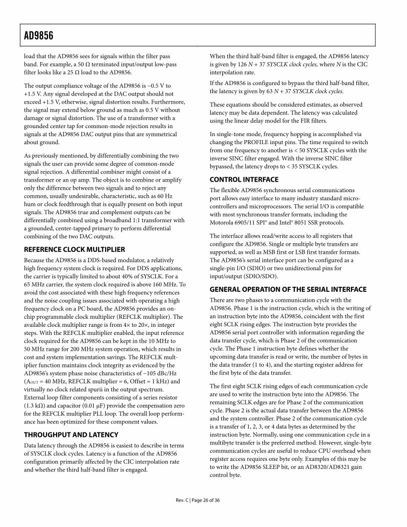
Instruction Byte .......................................................................... 27
Serial Interface Port Pin Descriptions ..................................... 28
MSB/LSB Transfers .................................................................... 28
Notes on Serial Port Operation ................................................ 28
Programming/Writing the AD8320/AD8321 Cable Driver Amplifier Gain Control ............................................................. 30
Understanding and Using Pin-Selectable Modulator Profiles....................................................................................................... 31
Power Dissipation Considerations........................................... 31
AD9856 Evaluation Board ........................................................ 32
Support ........................................................................................ 32
Outline Dimensions ....................................................................... 35
Ordering Guide .......................................................................... 35
REVISION HISTORY
1/05—Rev. B to Rev. C Updated Format..................................................................Universal Changes to Table 2............................................................................ 5 Changes to Input Word Rate (fw) vs. REFCLK Relationship Section.................................................................. 16 Changes to Cascaded Integrator Comb (CIC) Filter Section ... 21 Updates to Direct Digital Synthesizer Function Section........... 25 Added Support Section.................................................................. 32 Updated Outline Dimensions ....................................................... 35 Changes to Ordering Guide .......................................................... 35
9/99—Rev. A to Rev. B
AD9856
Rev. C | Page 3 of 36
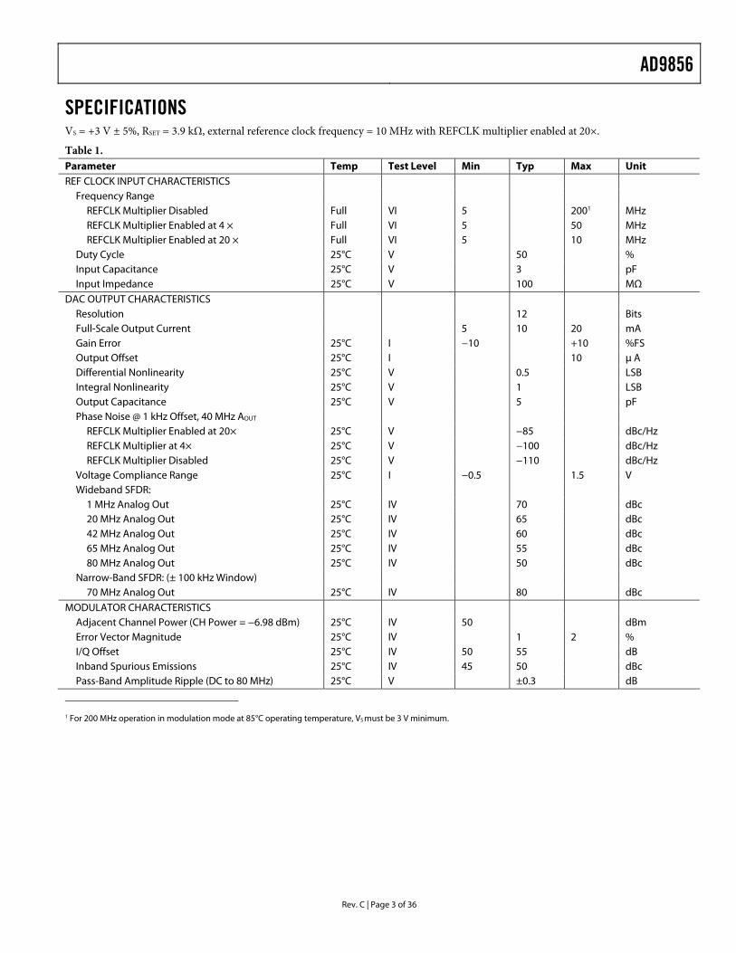
SPECIFICATIONS VS = +3 V ± 5%, RSET = 3.9 kΩ, external reference clock frequency = 10 MHz with REFCLK multiplier enabled at 20×.
Table 1. Parameter Temp Test Level Min Typ Max Unit REF CLOCK INPUT CHARACTERISTICS
Frequency Range REFCLK Multiplier Disabled Full VI 5 2001 MHz REFCLK Multiplier Enabled at 4 × Full VI 5 50 MHz REFCLK Multiplier Enabled at 20 × Full VI 5 10 MHz
Duty Cycle 25°C V 50 % Input Capacitance 25°C V 3 pF Input Impedance 25°C V 100 MΩ
DAC OUTPUT CHARACTERISTICS Resolution 12 Bits Full-Scale Output Current 5 10 20 mA Gain Error 25°C I −10 +10 %FS Output Offset 25°C I 10 µ A Differential Nonlinearity 25°C V 0.5 LSB Integral Nonlinearity 25°C V 1 LSB Output Capacitance 25°C V 5 pF Phase Noise @ 1 kHz Offset, 40 MHz AOUT
REFCLK Multiplier Enabled at 20× 25°C V −85 dBc/Hz REFCLK Multiplier at 4× 25°C V −100 dBc/Hz REFCLK Multiplier Disabled 25°C V −110 dBc/Hz
Voltage Compliance Range 25°C I −0.5 1.5 V Wideband SFDR:
1 MHz Analog Out 25°C IV 70 dBc 20 MHz Analog Out 25°C IV 65 dBc 42 MHz Analog Out 25°C IV 60 dBc 65 MHz Analog Out 25°C IV 55 dBc 80 MHz Analog Out 25°C IV 50 dBc
Narrow-Band SFDR: (± 100 kHz Window) 70 MHz Analog Out 25°C IV 80 dBc
MODULATOR CHARACTERISTICS Adjacent Channel Power (CH Power = −6.98 dBm) 25°C IV 50 dBm Error Vector Magnitude 25°C IV 1 2 % I/Q Offset 25°C IV 50 55 dB Inband Spurious Emissions 25°C IV 45 50 dBc Pass-Band Amplitude Ripple (DC to 80 MHz) 25°C V ±0.3 dB
1 For 200 MHz operation in modulation mode at 85°C operating temperature, VS must be 3 V minimum.
AD9856
Rev. C | Page 4 of 36
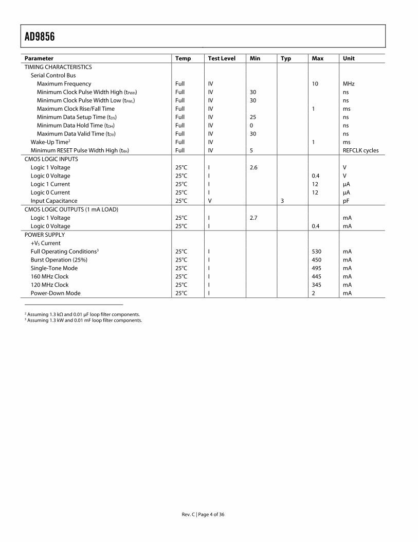
Parameter Temp Test Level Min Typ Max Unit TIMING CHARACTERISTICS
Serial Control Bus Maximum Frequency Full IV 10 MHz Minimum Clock Pulse Width High (tPWH) Full IV 30 ns Minimum Clock Pulse Width Low (tPWL) Full IV 30 ns Maximum Clock Rise/Fall Time Full IV 1 ms Minimum Data Setup Time (tDS) Full IV 25 ns Minimum Data Hold Time (tDH) Full IV 0 ns Maximum Data Valid Time (tDV) Full IV 30 ns
Wake-Up Time2 Full IV 1 ms Minimum RESET Pulse Width High (tRH) Full IV 5 REFCLK cycles
CMOS LOGIC INPUTS Logic 1 Voltage 25°C I 2.6 V Logic 0 Voltage 25°C I 0.4 V Logic 1 Current 25°C I 12 µA Logic 0 Current 25°C I 12 µA Input Capacitance 25°C V 3 pF
CMOS LOGIC OUTPUTS (1 mA LOAD) Logic 1 Voltage 25°C I 2.7 mA Logic 0 Voltage 25°C I 0.4 mA
POWER SUPPLY +VS Current Full Operating Conditions3 25°C I 530 mA Burst Operation (25%) 25°C I 450 mA Single-Tone Mode 25°C I 495 mA 160 MHz Clock 25°C I 445 mA 120 MHz Clock 25°C I 345 mA Power-Down Mode 25°C I 2 mA
2 Assuming 1.3 kΩ and 0.01 µF loop filter components. 3 Assuming 1.3 kW and 0.01 mF loop filter components.
AD9856
Rev. C | Page 5 of 36
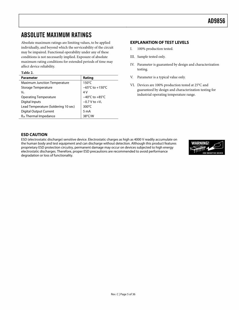
ABSOLUTE MAXIMUM RATINGS Absolute maximum ratings are limiting values, to be applied individually, and beyond which the serviceability of the circuit may be impaired. Functional operability under any of these conditions is not necessarily implied. Exposure of absolute maximum rating conditions for extended periods of time may affect device reliability.
Table 2. Parameter Rating Maximum Junction Temperature 150°C Storage Temperature −65°C to +150°C VS 4 V Operating Temperature −40°C to +85°C Digital Inputs −0.7 V to +Vs
Lead Temperature (Soldering 10 sec) 300°C Digital Output Current 5 mA θJA Thermal Impedance 38°C/W
EXPLANATION OF TEST LEVELS I. 100% production tested.
III. Sample tested only.
IV. Parameter is guaranteed by design and characterization testing.
V. Parameter is a typical value only.
VI. Devices are 100% production tested at 25°C and guaranteed by design and characterization testing for industrial operating temperature range.
ESD CAUTION ESD (electrostatic discharge) sensitive device. Electrostatic charges as high as 4000 V readily accumulate on the human body and test equipment and can discharge without detection. Although this product features proprietary ESD protection circuitry, permanent damage may occur on devices subjected to high energy electrostatic discharges. Therefore, proper ESD precautions are recommended to avoid performance degradation or loss of functionality.
AD9856
Rev. C | Page 6 of 36
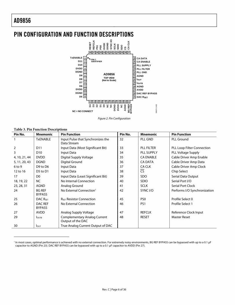
PIN CONFIGURATION AND FUNCTION DESCRIPTIONS
0063
7-C
-002
36
35
34
33
32
31
30
29
28
27
26
25
13 14 15 16 17 18 19 20 21 22 23 24
12
3
45
6
78
9
10
11
12
48 47 46 45 44 39 3843 42 41 40 37
PIN 1IDENTIFIER
TOP VIEW(Not to Scale)
AD9856
CA DATACA ENABLEPLL SUPPLYPLL FILTERPLL GNDAGNDIOUT
TxENABLED11D10
DVDDDGND
D9D8
NC = NO CONNECT
D7D6
DVDDDGND
IOUTBAGNDAVDDDAC REF BYPASS
BG
REF
BYP
ASS
D5 DAC RSET
NC
DVD
DD
GN
DN
CD0
D1
D2D3
D4
NC
AG
ND
SYN
C I/
O
CSREF
CLK
SCLK
RES
ET
PS0
DVD
DD
GN
D
CA
CLK
PS1
SDO
SDIO
Figure 2. Pin Configuration
Table 3. Pin Function Descriptions Pin No. Mnemonic Pin Function Pin No. Mnemonic Pin Function 1 TxENABLE Input Pulse that Synchronizes the
Data Stream 32 PLL GND PLL Ground
2 D11 Input Data (Most Significant Bit) 33 PLL FILTER PLL Loop Filter Connection 3 D10 Input Data 34 PLL SUPPLY PLL Voltage Supply 4, 10, 21, 44 DVDD Digital Supply Voltage 35 CA ENABLE Cable Driver Amp Enable 5, 11, 20, 43 DGND Digital Ground 36 CA DATA Cable Driver Amp Data 6 to 9 D9 to D6 Input Data 37 CA CLK Cable Driver Amp Clock 12 to 16 D5 to D1 Input Data 38 CS Chip Select
17 D0 Input Data (Least Significant Bit) 39 SDO Serial Data Output 18, 19, 22 NC No Internal Connection 40 SDIO Serial Port I/O 23, 28, 31 AGND Analog Ground 41 SCLK Serial Port Clock 24 BG REF
BYPASS No External Connection1 42 SYNC I/O Performs I/O Synchronization
25 DAC RSET RSET Resistor Connection 45 PS0 Profile Select 0 26 DAC REF
BYPASS No External Connection1 46 PS1 Profile Select 1
27 AVDD Analog Supply Voltage 47 REFCLK Reference Clock Input 29 IOUTB Complementary Analog Current
Output of the DAC 48 RESET Master Reset
30 IOUT True Analog Current Output of DAC
1 In most cases, optimal performance is achieved with no external connection. For extremely noisy environments, BG REF BYPASS can be bypassed with up to a 0.1 µF
capacitor to AGND (Pin 23). DAC REF BYPASS can be bypassed with up to a 0.1 µF capacitor to AVDD (Pin 27).
AD9856
Rev. C | Page 7 of 36
Table 4. Functional Block Mode Descriptions Functional Block Mode Description Operating Modes 1. Complex quadrature modulator mode.
2. Single-tone output mode. Input Data Format Programmable: 12-bit, 6-bit, or 3-bit input formats. Data input to the AD9856 is 12-bit, twos complement. Complex
I/Q symbol component data is required to be at least 2× oversampled, depending upon configuration. Input Sample Rate Up to 50 Msamples/sec @ 200 MHz SYSCLK rate. Input Reference Clock Frequency
For DC to 80 MHz AOUT operation (200 MHz SYSCLK rate) with REFCLK multiplier enabled: 10 MHz to50 MHz, programmable via control bus; with REFCLK multiplier disabled: 200 MHz. Note: For optimum data synchronization, the AD9856 reference clock and the input data clock should be derived from the same clock source.
Internal Reference Clock Multiplier
Programmable in integer steps over the range of 4× to 20×. Can be disabled (effective REFCLK multiplier = 1) via control bus. Output of REFCLK multiplier = SYSCLK rate, which is the internal clock rate applied to the DDS and DAC function.
Profile Select Four pin-selectable, preprogrammed formats. Available for modulation and single-tone operating modes. Interpolating Range Fixed 4×, selectable 2×, and selectable 2× to 63× range. Half-Band Filters Interpolating filters that provide upsampling and reduce the effects of the CIC passband roll-off characteristics. TxENABLE Function–Burst Mode
When burst mode is enabled via the control bus, the rising edge of the applied TxENABLE pulse should be coincident with, and frame, the input data packet. This establishes data sampling synchronization.
TxENABLE Function–Continuous Mode
When continuous mode is enabled via the control bus, the TxENABLE pin becomes an I/Q control line. A Logic 1 on TxENABLE indicates I data is being presented to the AD9856. A Logic 0 on TxENABLE indicates Q data is being presented to the AD9856. Each rising edge of TxENABLE resynchronizes the AD9856 input sampling capability.
Inverse SINC Filter Precompensates for SIN(x)/x roll-off of DAC; user bypassable. I/Q Channel Invert [I ×Cos(ωt) + Q ×Sin(ωt)] or [I ×Cos(ωt) − Q ×Sin(ωt)] (default), configurable via control bus, per profile. Full Sleep Mode Power dissipation reduced to less than 6 mW when full sleep mode is active; programmable via the control bus.
AD9856
Rev. C | Page 8 of 36
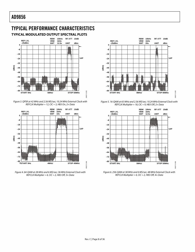
TYPICAL PERFORMANCE CHARACTERISTICS TYPICAL MODULATED OUTPUT SPECTRAL PLOTS
–80
–72
–64
–56
–48
–40
–32
–24
–16
–8
0
(dB
m)
STOP 50MHzSTART 0Hz 5MHz/
REF LVL–25dBm
RBWVBWSWT
10dB
dBm
RF ATT
UNIT
10kHz1kHz12.5s
1AP
0063
7-C
-003
Figure 3. QPSK at 42 MHz and 2.56 MS/sec; 10.24 MHz External Clock with REFCLK Multiplier = 12, CIC = 3, HB3 On, 2× Data
–80
–72
–64
–56
–48
–40
–32
–24
–16
–8
0
(dB
m)
STOP 40MHzSTART 0Hz 4MHz/
REF LVL–30dBm
RBWVBWSWT
10dB
dBm
RF ATT
UNIT
10kHz1kHz10s
1AP
0063
7-C
-0040
Figure 4. 64-QAM at 28 MHz and 6 MS/sec; 36 MHz External Clock with REFCLK Multiplier = 4, CIC = 2, HB3 Off, 3× Data
–80
–72
–64
–56
–48
–40
–32
–24
–16
–8
0
(dB
m)
STOP 80MHzSTART 0Hz 8MHz/
REF LVL–25dBm
RBWVBWSWT
10dB
dBm
RF ATT
UNIT
10kHz1kHz20s
1AP
0063
7-C
-005
Figure 5. 16-QAM at 65 MHz and 2.56 MS/sec; 10.24 MHz External Clock with REFCLK Multiplier = 18, CIC = 9, HB3 Off, 2× Data
–80
–72
–64
–56
–48
–40
–32
–24
–16
–8
0
(dB
m)
STOP 50MHzSTART 0Hz 5MHz/
REF LVL–30dBm
RBWVBWSWT
10dB
dBm
RF ATT
UNIT
10kHz1kHz12.5s
1AP
0063
7-C
-006
Figure 6. 256-QAM at 38 MHz and 6 MS/sec; 48 MHz External Clock with REFCLK Multiplier = 4, CIC = 2, HB3 Off, 4× Data
AD9856
Rev. C | Page 9 of 36
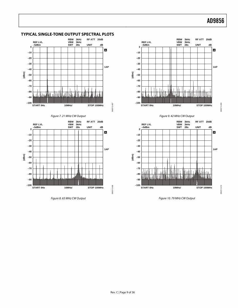
TYPICAL SINGLE-TONE OUTPUT SPECTRAL PLOTS
–100
–90
–80
–70
–60
–50
–40
–30
–20
–10
0
(dB
m)
STOP 100MHzSTART 0Hz 10MHz/
REF LVL–5dBm
RBWVBWSWT
RF ATT
UNIT
3kHz3kHz28s
20dB
dB
1AP
A
0063
7-C
-007
Figure 7. 21 MHz CW Output
–100
–90
–80
–70
–60
–50
–40
–30
–20
–10
0
(dB
m)
STOP 100MHzSTART 0Hz 10MHz/
REF LVL–5dBm
RBWVBWSWT
RF ATT
UNIT
3kHz3kHz28s
20dB
dB
1AP
A
0063
7-C
-008
Figure 8. 65 MHz CW Output
–100
–90
–80
–70
–60
–50
–40
–30
–20
–10
0
(dB
m)
STOP 100MHzSTART 0Hz 10MHz/
REF LVL–5dBm
RBWVBWSWT
RF ATT
UNIT
3kHz3kHz28s
20dB
dB
1AP
A
0063
7-C
-009
Figure 9. 42 MHz CW Output
–100
–90
–80
–70
–60
–50
–40
–30
–20
–10
0(d
Bm
)
STOP 100MHzSTART 0Hz 10MHz/
REF LVL–5dBm
RBWVBWSWT
RF ATT
UNIT
3kHz3kHz28s
20dB
dB
1AP
A
0063
7-C
-010
Figure 10. 79 MHz CW Output
AD9856
Rev. C | Page 10 of 36
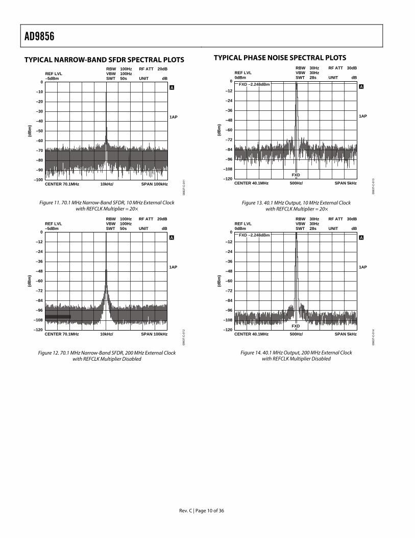
TYPICAL NARROW-BAND SFDR SPECTRAL PLOTS
–100
–90
–80
–70
–60
–50
–40
–30
–20
–10
0
(dB
m)
SPAN 100kHzCENTER 70.1MHz 10kHz/
REF LVL–5dBm
RBWVBWSWT
20dB
dB
RF ATT
UNIT
100Hz100Hz50s
1AP
A
0063
7-C
-011
Figure 11. 70.1 MHz Narrow-Band SFDR, 10 MHz External Clock with REFCLK Multiplier = 20×
–120
–108
–96
–84
–72
–60
–48
–36
–24
–12
0
(dB
m)
SPAN 100kHzCENTER 70.1MHz 10kHz/
REF LVL–5dBm
RBWVBWSWT
20dBRF ATT
UNIT
100Hz100Hz50s dB
1AP
A
0063
7-C
-012
Figure 12. 70.1 MHz Narrow-Band SFDR, 200 MHz External Clock with REFCLK Multiplier Disabled
TYPICAL PHASE NOISE SPECTRAL PLOTS
–120
–108
–96
–84
–72
–60
–48
–36
–24
–12
0
(dB
m)
SPAN 5kHzCENTER 40.1MHz 500Hz/
REF LVL0dBm
RBWVBWSWT
30dB
dB
RF ATT
UNIT
30Hz30Hz28s
1AP
AFXD –2.248dBm
FXD
0063
7-C
-013
Figure 13. 40.1 MHz Output, 10 MHz External Clock with REFCLK Multiplier = 20×
–120
–108
–96
–84
–72
–60
–48
–36
–24
–12
0
(dB
m)
SPAN 5kHzCENTER 40.1MHz 500Hz/
REF LVL0dBm
RBWVBWSWT
30dBRF ATT
UNIT
30Hz30Hz28s dB
1AP
AFXD –2.248dBm
FXD
0063
7-C
-014
Figure 14. 40.1 MHz Output, 200 MHz External Clock with REFCLK Multiplier Disabled
AD9856
Rev. C | Page 11 of 36
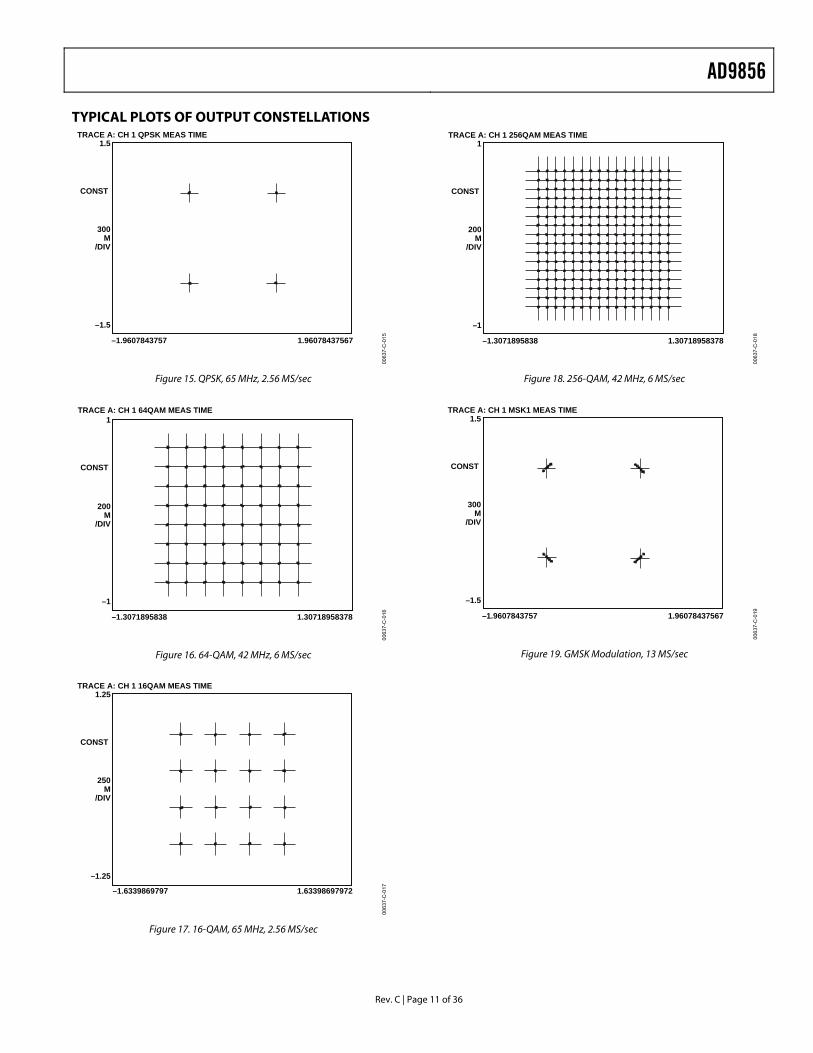
TYPICAL PLOTS OF OUTPUT CONSTELLATIONS
0063
7-C
-015–1.9607843757 1.96078437567
1.5TRACE A: CH 1 QPSK MEAS TIME
CONST
300M
/DIV
–1.5
Figure 15. QPSK, 65 MHz, 2.56 MS/sec
0063
7-C
-016–1.3071895838 1.30718958378
1TRACE A: CH 1 64QAM MEAS TIME
CONST
200M
/DIV
–1
Figure 16. 64-QAM, 42 MHz, 6 MS/sec
0063
7-C
-017–1.6339869797 1.63398697972
1.25TRACE A: CH 1 16QAM MEAS TIME
CONST
250M
/DIV
–1.25
Figure 17. 16-QAM, 65 MHz, 2.56 MS/sec
0063
7-C
-018–1.3071895838 1.30718958378
1TRACE A: CH 1 256QAM MEAS TIME
CONST
200M
/DIV
–1
Figure 18. 256-QAM, 42 MHz, 6 MS/sec
0063
7-C
-019–1.9607843757 1.96078437567
1.5TRACE A: CH 1 MSK1 MEAS TIME
CONST
300M
/DIV
–1.5
Figure 19. GMSK Modulation, 13 MS/sec
AD9856
Rev. C | Page 12 of 36
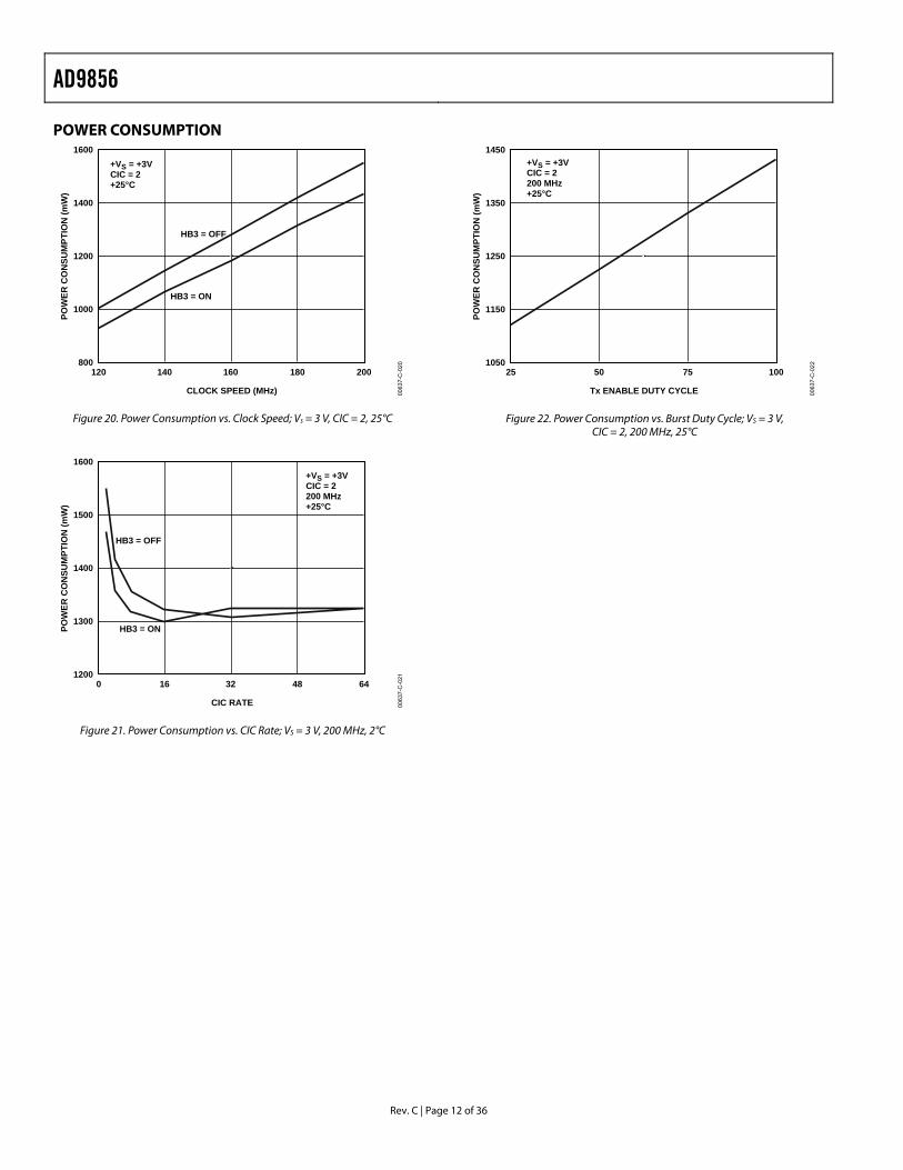
POWER CONSUMPTION
POW
ER C
ON
SUM
PTIO
N (m
W)
800
1000
1200
1400
1600
CLOCK SPEED (MHz)
140120 160 180 200
0063
7-C
-020
HB3 = OFF
HB3 = ON
+VS = +3VCIC = 2+25°C
Figure 20. Power Consumption vs. Clock Speed; Vs = 3 V, CIC = 2, 25°C
POW
ER C
ON
SUM
PTIO
N (m
W)
1200
1300
1400
1500
1600
CIC RATE
160 32 48
0063
7-C
-021
HB3 = OFF
HB3 = ON
+VS = +3VCIC = 2200 MHz+25°C
64
Figure 21. Power Consumption vs. CIC Rate; VS = 3 V, 200 MHz, 2°C
POW
ER C
ON
SUM
PTIO
N (m
W)
1050
1150
1250
1350
1450
Tx ENABLE DUTY CYCLE
25 7550 100
0063
7-C
-022
+VS = +3VCIC = 2200 MHz+25°C
Figure 22. Power Consumption vs. Burst Duty Cycle; VS = 3 V, CIC = 2, 200 MHz, 25°C
AD9856
Rev. C | Page 13 of 36
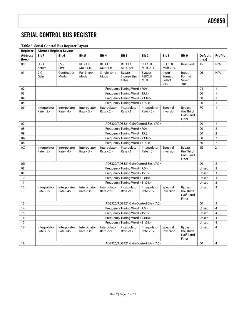
SERIAL CONTROL BUS REGISTER Table 5. Serial Control Bus Register Layout Register AD9856 Register Layout
Address (hex)
Bit 7 Bit 6 Bit 5 Bit 4 Bit 3 Bit 2 Bit 1 Bit 0 Default (hex)
Profile
00 SDO Active
LSB First
REFCLK Mult.<4>
REFCLK Mult.<3>
REFCLK Mult.<2>
REFCLK Mult.<1>
REFCLK Mult.<0>
Reserved 15 N/A
01 CIC Gain
Continuous Mode
Full Sleep Mode
Single-tone Mode
Bypass Inverse Sinc Filter
Bypass REFCLK Mult.
Input Format Select <1>
Input Format Select <0>
06 N/A
02 Frequency Tuning Word <7:0> 04 1
03 Frequency Tuning Word <15:8> 00 1
04 Frequency Tuning Word <23:16> 00 1
05 Frequency Tuning Word <31:24> 00 1
06 Interpolator Rate <5>
Interpolator Rate <4>
Interpolator Rate <3>
Interpolator Rate <2>
Interpolator Rate <1>
Interpolator Rate <0>
Spectral Inversion
Bypass the Third Half-Band Filter
FC 1
07 AD8320/AD8321 Gain Control Bits <7:0> 00 1
08 Frequency Tuning Word <7:0> 00 2
09 Frequency Tuning Word <15:8> 00 2
0A Frequency Tuning Word <23:16> 00 2
0B Frequency Tuning Word <31:24> 80 2
0C Interpolator Rate <5>
Interpolator Rate <4>
Interpolator Rate <3>
Interpolator Rate <2>
Interpolator Rate <1>
Interpolator Rate <0>
Spectral Inversion
Bypass the Third Half-Band Filter
1E 2
0D AD8320/AD8321 Gain Control Bits <7:0> 00 2
0E Frequency Tuning Word <7:0> Unset 3
0F Frequency Tuning Word <15:8> Unset 3
10 Frequency Tuning Word <23:16> Unset 3
11 Frequency Tuning Word <31:24> Unset 3
12 Interpolator Rate <5>
Interpolator Rate <4>
Interpolator Rate <3>
Interpolator Rate <2>
Interpolator Rate <1>
Interpolator Rate <0>
Spectral Inversion
Bypass the Third Half-Band Filter
Unset 3
13 AD8320/AD8321 Gain Control Bits <7:0> 00 3
14 Frequency Tuning Word <7:0> Unset 4
15 Frequency Tuning Word <15:8> Unset 4
16 Frequency Tuning Word <23:16> Unset 4
17 Frequency Tuning Word <31:24> Unset 4
18 Interpolator Rate <5>
Interpolator Rate <4>
Interpolator Rate <3>
Interpolator Rate <2>
Interpolator Rate <1>
Interpolator Rate <0>
Spectral Inversion
Bypass the Third Half-Band Filter
Unset 4
19 AD8320/AD8321 Gain Control Bits <7:0> 00 4
AD9856
Rev. C | Page 14 of 36
REGISTER BIT DEFINITIONSControl Bits—Register Address 00h and 01h
SDO Active—Register Address 00h, Bit 7. Active high indicates serial port uses dedicated in/out lines. Default low configures serial port as single-line I/O.
LSB First—Register Address 00h, Bit 6. Active high indicates serial port access is LSB-to-MSB format. Default low indicates MSB-to-LSB format.
REFCLK Multiplier—Register Address 00h, Bits 5, 4, 3, 2, 1 form the reference clock multiplier. Valid entries range from 4–20 (decimal). Straight binary to decimal conversion is implemented. For example, to multiply the reference clock by 19 decimal, Program Register Address 00h, Bits 5–1, as 13h. Default value is 0A (hex).
Reserved Bit—Register Address 00h, Bit 0. This bit is reserved. Always set this bit to Logic 1 when writing to this register.
CIC Gain—Register Address 01h, Bit 7. The CIC GAIN bit multiplies the CIC filter output by 2. See the Cascaded Integrator Comb (CIC) Filter section for more details. Default value is 0 (inactive).
Continuous Mode—Register Address 01h, Bit 6 is the continuous mode configuration bit. Active high configures the AD9856 to accept continuous-mode timing on the TxENABLE input. A low configures the device for burst-mode timing. Default value is 0 (burst mode).
Full Sleep Mode—Register Address 01h, Bit 5. Active high full sleep mode bit. When activated, the AD9856 enters a full shutdown mode, consuming less than 2 mA after completing a shutdown sequence. Default value is 0 (awake).
Single-Tone Mode—Register Address 01h, Bit 4. Active high configures the AD9856 for single-tone applications. The AD9856 supplies a single-frequency output as determined by the frequency tuning word (FTW) selected by the active profile. In this mode, the 12 input data pins are ignored but should be tied high or low. Default value is 0 (inactive).
Bypass Inverse Sinc Filter—Register Address 01h, Bit 3. Active high configures the AD9856 to bypass the SIN(x)/x compensation filter. Default value is 0 (inverse SINC filter enabled).
Bypass REFCLK Multiplier—Register Address 01h, Bit 2. Active high configures the AD9856 to bypass the REFCLK multiplier function. When active, effectively causes the REFCLK multiplier factor to be 1. Default value is 1 (REFCLK multiplier bypassed).
Input Format Select—Register Address 01h, Bits 1 and 0, form the input format mode bits.
10b = 12-bit mode 01b = 6-bit mode 00b = 3-bit mode
Default value is 10b (12-bit mode).
Profile 1 Registers—Active when PROFILE Inputs are 00b
Frequency Tuning Word (FTW)—The frequency tuning word for Profile 1 is formed via a concatenation of register addresses 05h, 04h, 03h, and 02h. Bit 7 of Register Address 05h is the most significant bit of the Profile 1 frequency tuning word. Bit 0 of Register Address 02h is the least significant bit of the Profile 1 frequency tuning word. The output frequency equation is given as: fOUT = (FTW SYSCLK)/232.
Interpolation Rate—Register Address 06h, Bit 7 through Bit 2 form the Profile 1 CIC filter interpolation rate value. Allowed values range from 2 to 63 (decimal).
Spectral Inversion—Register Address 06h, Bit 1. Active high, Profile 1 spectral inversion bit. When active, inverted modulation is performed [I Cos(ωt) + Q × Sin( t)]. The Default is inactive, Logic 0, noninverted modulation [I × Cos(ωt) − Q × Sin(ωt)].
Bypass Half-Band Filter 3—Register Address 06h, Bit 0. Active high, causes the AD9856 to bypass the third half-band filter stage that precedes the CIC interpolation filter. Bypassing the third half-band filter negates the 2× upsample inherent with this filter and reduces the overall interpolation rate of the half-band filter chain from 8× to 4×. Default value is 0 (Half-Band 3 enabled).
AD8320/AD8321 Gain Control—Register Address 07h, Bit 7 through Bit 0 form the Profile 1 AD8320/AD8321 gain bits. The AD9856 dedicates three output pins, which directly interface to the AD8320/AD8321 cable driver amp. This allows direct control of the cable driver via the AD9856. See the Error! Reference source not found. section for more details. Bit 7 is the MSB, Bit 0 is the LSB. Default value is 00h.
Profile 2 Registers—Active when PROFILE Inputs are 01b Profile 2 register functionality is identical to Profile 1, with the exception of the register addresses.
Profile 3 Registers—Active when PROFILE Inputs are 10b Profile 3 register functionality is identical to Profile 1, with the exception of the register addresses.
Profile 4 Registers—Active when PROFILE Inputs are 11b Profile 4 register functionality is identical to Profile 1, with the exception of the register addresses.
AD9856
Rev. C | Page 15 of 36
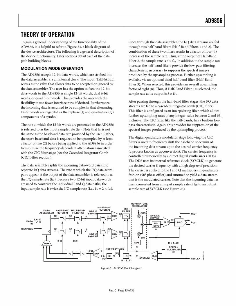
THEORY OF OPERATION To gain a general understanding of the functionality of the AD9856, it is helpful to refer to Figure 23, a block diagram of the device architecture. The following is a general description of the device functionality. Later sections detail each of the data path building blocks.
MODULATION MODE OPERATION The AD9856 accepts 12-bit data-words, which are strobed into the data assembler via an internal clock. The input, TxENABLE, serves as the valve that allows data to be accepted or ignored by the data assembler. The user has the option to feed the 12-bit data-words to the AD9856 as single 12-bit words, dual 6-bit words, or quad 3-bit words. This provides the user with the flexibility to use fewer interface pins, if desired. Furthermore, the incoming data is assumed to be complex in that alternating 12-bit words are regarded as the inphase (I) and quadrature (Q) components of a symbol.
The rate at which the 12-bit words are presented to the AD9856 is referred to as the input sample rate (fIN). Note that fIN is not the same as the baseband data rate provided by the user. Rather, the user’s baseband data is required to be upsampled by at least a factor of two (2) before being applied to the AD9856 in order to minimize the frequency-dependent attenuation associated with the CIC filter stage (see the Cascaded Integrator Comb (CIC) Filter section ).
The data assembler splits the incoming data-word pairs into separate I/Q data streams. The rate at which the I/Q data-word pairs appear at the output of the data assembler is referred to as the I/Q sample rate (fIQ). Because two 12-bit input data-words are used to construct the individual I and Q data paths, the input sample rate is twice the I/Q sample rate (i.e., fIN = 2 × fIQ).
Once through the data assembler, the I/Q data streams are fed through two half-band filters (Half-Band Filters 1 and 2). The combination of these two filters results in a factor of four (4) increase of the sample rate. Thus, at the output of Half-Band Filter 2, the sample rate is 4 × fIQ. In addition to the sample rate increase, the half-band filters provide the low-pass filtering characteristic necessary to suppress the spectral images produced by the upsampling process. Further upsampling is available via an optional third half-band filter (Half-Band Filter 3). When selected, this provides an overall upsampling factor of eight (8). Thus, if Half-Band Filter 3 is selected, the sample rate at its output is 8 × fIQ.
After passing through the half-band filter stages, the I/Q data streams are fed to a cascaded integrator comb (CIC) filter. This filter is configured as an interpolating filter, which allows further upsampling rates of any integer value between 2 and 63, inclusive. The CIC filter, like the half-bands, has a built-in low-pass characteristic. Again, this provides for suppression of the spectral images produced by the upsampling process.
The digital quadrature modulator stage following the CIC filters is used to frequency shift the baseband spectrum of the incoming data stream up to the desired carrier frequency (a process known as upconversion). The carrier frequency is controlled numerically by a direct digital synthesizer (DDS). The DDS uses its internal reference clock (SYSCLK) to generate the desired carrier frequency with a high degree of precision. The carrier is applied to the I and Q multipliers in quadrature fashion (90° phase offset) and summed to yield a data stream that is the modulated carrier. Note that the incoming data has been converted from an input sample rate of fIN to an output sample rate of SYSCLK (see Figure 23).
0063
7-C
-023
DATAIN
TxENABLE
DATAASSEMBLER
HALF-BANDFILTER #1
HALF-BANDFILTER #2
I
Q
HALF-BANDFILTER #3
12
12
12
DDS
INVSINC
INV SINCBYPASS
RSET
AOUT
M = 4...20
REFCLKN = 2...63
(SYSCLK)(F4)
(F3)
(F2)(F1)
3, 6, 12MUX1212
12
COS
SIN
CICFILTER
QUADRATUREMODULATOR
MUX12
DAC
12
12 1212
HBF #3BYPASS
HBF #3BYPASS
MUX
MUX
÷2 ÷2 MUX
HBF #3 BYPASS
÷N(F5)
MUX
REFCLKMULTIPLIER
(M)
÷2
Figure 23. AD9856 Block Diagram
AD9856
Rev. C | Page 16 of 36
The sampled carrier is ultimately destined to serve as the input data to the digital-to-analog converter (DAC) integrated on the AD9856. The DAC output spectrum is distorted due to the intrinsic zero-order hold effect associated with DAC-generated signals. This distortion is deterministic, however, and follows the familiar SIN(x)/x (or SINC) envelope. Because the SINC distortion is predictable, it is also correctable—therefore, the presence of the optional inverse SINC filter preceding the DAC. This is a FIR filter, which has a transfer function conforming to the inverse of the SINC response. Thus, when selected, it modifies the incoming data stream so that the SINC distortion, which would otherwise appear in the DAC output spectrum, is virtually eliminated.
As mentioned earlier, the output data is sampled at the rate of SYSCLK. Because the AD9856 is designed to operate at SYSCLK frequencies up to 200 MHz, there is the potential difficulty of trying to provide a stable input clock (REFCLK). Although stable, commercial high frequency oscillators tend to be cost prohibitive. To alleviate this problem, the AD9856 has a built-in programmable clock multiplier circuit. This allows the user to use a relatively low frequency (thus, less expensive) oscillator to generate the REFCLK signal. The low frequency REFCLK signal can then be multiplied in frequency by an integer factor between 4 and 20, inclusive, to become the SYSCLK signal.
Single-Tone Output Operation
The AD9856 can be configured for frequency synthesis applications by writing the single-tone bit true. In single-tone mode, the AD9856 disengages the modulator and preceding data path logic to output a spectrally pure, single-frequency sine wave. The AD9856 provides for a 32-bit frequency tuning word, which results in a tuning resolution of 0.046 Hz at a SYSCLK rate of 200 MHz.
When using the AD9856 as a frequency synthesizer, a general rule is to limit the fundamental output frequency to 40% of SYSCLK. This avoids generating aliases too close to the desired fundamental output frequency, thus minimizing the cost of filtering the aliases.
All applicable programming features of the AD9856 apply when configured in single-tone mode. These features include:
• Frequency hopping via the profile inputs and associated tuning word, which allows frequency shift keying (FSK) modulation.
• Ability to bypass the REFCLK multiplier, which results in lower phase noise and reduced output jitter.
• Ability to bypass the SIN(x)/x compensation filter. • Full power-down mode.
INPUT WORD RATE (FW) vs. REFCLK RELATIONSHIP There is a fundamental relationship between the input word rate (fW) and the frequency of the clock that serves as the timing source for the AD9856 (REFCLK). The fW is defined as the rate at which K-bit data-words (K = 3, 6, or 12) are presented to the AD9856. However, the following factors affect this relationship: • The interpolation rate of the CIC filter stage. • Whether or not Half-Band Filter 3 is bypassed. • The value of the REFCLK multiplier (if selected). • Input word length.
This relationship can be summed as ( ) MIHNfREFCLK W /2=
where H, N, I, and M are integers determined as follows:
H = 1: Half-Band Filter 3 bypassed 2: Half-Band Filter 3 enabled M = 1: REFCLK multiplier bypassed 4 ≤ M ≤ 20: REFCLK multiplier enabled I = 1: Full-word input format 2: Half-word input format 4: Quarter-Word input format N = CIC interpolation rate (2 ≤ N ≤ 63)
These conditions show that REFCLK and fW have an integer ratio relationship. It is very important that users choose a value of REFCLK to ensure that this integer ratio relationship is maintained.
I/Q DATA SYNCHRONIZATION As mentioned previously, the AD9856 accepts I/Q data pairs and a twos complement numbering system in three different word length modes. The full-word mode accepts 12-bit parallel I and Q data. The half-word mode accepts dual 6-bit I and Q data inputs to form a 12-bit word. The quarter-word mode accepts multiple 3-bit I and Q data inputs to form a 12-bit word. For all word length modes, the AD9856 assembles the data for signal processing into time-aligned, parallel, 12-bit I/Q pairs. In addition to the word length flexibility, the AD9856 has two input timing modes, burst or continuous, that are programmable via the serial port.
For burst-mode input timing, no external data clock needs to be provided, because the data is oversampled at the D<11:0> pins using the system clock (SYSCLK). The TxENABLE pin is required to frame the data burst, because the rising edge of TxENABLE is used to synchronize the AD9856 to the input data rate. The AD9856 registers the input data at the approx-imate center of the data valid time. Thus, for larger CIC interpolation rates, more SYSCLK cycles are available to oversample the input data, maximizing clock jitter tolerances.
AD9856
Rev. C | Page 17 of 36
For continuous-mode input timing, the TxENABLE pin can be thought of as a data input clock running at half the input sample rate (fW/2). In addition to synchronization, for contin-uous mode timing, the TxENABLE input indicates whether an I or Q input is being presented to the D<11:0> pins. It is intended that data is presented in alternating fashion such that I data is followed by Q data. Stated another way, the TxENABLE pin should maintain approximately a 50/50 duty cycle. As in burst mode, the rising edge of TxENABLE synchronizes the AD9856 to the input data rate and the data is registered at the approximate center of the data-valid time. The continuous operating mode can only be used in conjunction with the full-word input format.
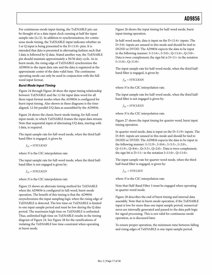
Burst Mode Input Timing
Figure 24 through Figure 28 show the input timing relationship between TxENABLE and the 12-bit input data-word for all three input format modes when the AD9856 is configured for burst input timing. Also shown in these diagrams is the time-aligned, 12-bit parallel I/Q data as assembled by the AD9856.
Figure 24 shows the classic burst-mode timing, for full-word input mode, in which TxENABLE frames the input data stream. Note that sequential input of alternating I/Q data, starting with I data, is required.
The input sample rate for full-word mode, when the third half-band filter is engaged, is given by
NSYSCLKfIN 4/=
where N is the CIC interpolation rate.
The input sample rate for full-word mode, when the third half-band filter is not engaged is given by:
NSYSCLKfIN 2/=
where N is the CIC interpolation rate
Figure 25 shows an alternate timing method for TxENABLE when the AD9856 is configured in full-word, burst-mode operation. The benefit of this timing is that the AD9856 resynchronizes the input sampling logic when the rising edge of TxENABLE is detected. The low time on TxENABLE is limited to one input sample period and must be low during the Q data period. The maximum high time on TxENABLE is unlimited. Thus, unlimited high time on TxENABLE results in the timing diagram of Figure 24. See Figure 28 for the ramifications of violating the TxENABLE low time constraint when operating in burst mode.
Figure 26 shows the input timing for half-word mode, burst input timing operation.
In half-word mode, data is input on the D<11:6> inputs. The D<5:0> inputs are unused in this mode and should be tied to DGND or DVDD. The AD9856 expects the data to be input in the following manner: I<11:6>, I<5:0>, Q<11:6>, Q<5:0>. Data is twos complement; the sign bit is D<11> in the notation I<11:0>, Q<11:0>.
The input sample rate for half-word mode, when the third half-band filter is engaged, is given by
NSYSCLKfIN 4/=
where N is the CIC interpolation rate.
The input sample rate for half-word mode, when the third half-band filter is not engaged is given by:
NSYSCLKfIN 2/=
where N is the CIC interpolation rate.
Figure 27 shows the input timing for quarter-word, burst input timing operation.
In quarter-word mode, data is input on the D<11:9> inputs. The D<8:0> inputs are unused in this mode and should be tied to DGND or DVDD. The AD9856 expects the data to be input in the following manner: I<11:9>, I<8:6>, I<5:3>, I<2:0>, Q<11:9>, Q<8:6>, Q<5:3>, Q<2:0>. Data is twos complement; the sign bit is D<11> in the notation I<11:0>, Q<11:0>.
The input sample rate for quarter-word mode, when the third half-band filter is engaged, is given by:
NSYSCLKf IN /=
where N is the CIC interpolation rate.
Note that Half-Band Filter 3 must be engaged when operating in quarter-word mode.
Figure 28 describes the end of burst timing and internal data assembly. Note that in burst-mode operation, if the TxENABLE input is low for more than one input sample period, numerical zeros are internally generated and passed to the data path logic for signal processing. This is not valid for continuous-mode operation, as is discussed later.
To ensure proper operation, the minimum time between falling and rising edges of TxENABLE is one input sample period.
AD9856
Rev. C | Page 18 of 36
0063
7-C
-024
TxENABLE
D(11:0)
INTERNAL I
INTERNAL Q
I0 Q0 I1 Q1 I2 Q2 I3 Q3 I4 Q4
I0 I1 I2 I3
Q0 Q2 Q3Q1
Figure 24. 12-Bit Input Mode, Classic Burst Timing
0063
7-C
-025
TxENABLE
D(11:0)
INTERNAL I
INTERNAL Q
I0 Q0 I1 Q1 I2 Q2 I3 Q3 I4 Q4
I0 I1 I2 I3
Q0 Q1 Q2 Q3
Figure 25. 12-Bit Input Mode, Alternate TxENABLE Timing
0063
7-C
-026
TxENABLE
D(11:6)
INTERNAL I
INTERNAL Q
I0 I1
Q0 Q1
I0(11:6) I0(5:0) Q0(5:0) I1(11:6) I1(5:0) Q1(11:6) Q1(5:0) I2(11:6)Q0(11:6) I2(5:0)
Figure 26. 6-Bit Input Mode, Burst Mode Timing
0063
7-C
-027
I0(11:9) I0(8:6) I0(5:3) I0(2:0) Q0(11:9) Q0(8:6) Q0(5:3) Q0(2:0) I1(11:9) I1(8:6)
TxENABLE
D(11:9)
INTERNAL I
INTERNAL Q
I0
Q0
Figure 27. 3-Bit Input Mode, Burst Mode Timing
0063
7-C
-028
TxENABLE
D(11:0)
INTERNAL I
INTERNAL Q
IN QN I0 Q0 I1 Q1
ININ–2 IN–1
QN–2 QN–1 QN
LOGIC 0
LOGIC 0
I0
Q0
Figure 28. End of Burst Mode Input Timing
AD9856
Rev. C | Page 19 of 36
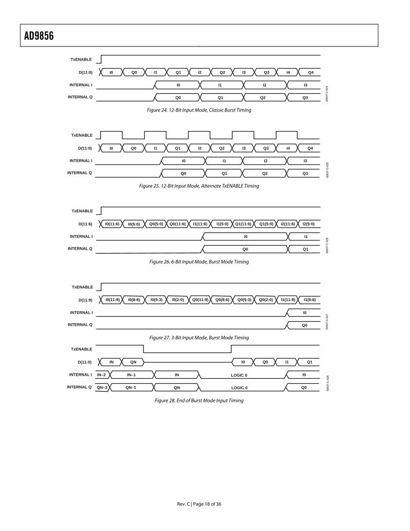
Continuous Mode Input Timing
The AD9856 is configured for continuous mode input timing by writing the continuous mode bit true (Logic 1). The continuous mode bit is in register address 01h, Bit 6. The AD9856 must be configured for full-word input format when operating in continuous mode input timing. The input data rate equations described previously for full-word mode apply for continuous mode. Figure 25, which is the alternate burst mode timing diagram, is also the continuous mode input timing. Figure 29 and Figure 30 show what the internal data assembler presents to the signal processing logic when the TxENABLE input is held static for greater than one input sample period. Please note that the timing diagram shown in Figure 29 and Figure 30 detail INCORRECT timing relationships between TxENABLE and data. They are only presented to indicate that the AD9856 resynchronizes properly after detecting a rising
edge of TxENABLE. Also note that the significant difference between burst and continuous mode operation is that in addition to synchronizing the data, TxENABLE is used to indicate whether an I or Q input is being sampled.
Do not engage continuous mode simultaneously with the REFCLK multiplier function. This corrupts the CIC inter-polating filter, forcing unrecoverable mathematical overflow that can only be resolved by issuing a RESET command. The problem is due to the PLL failing to be locked to the reference clock while nonzero data is being clocked into the interpolation stages from the data inputs. The recommended sequence is to first engage the REFCLK multiplier function (allowing at least 1 ms for loop stabilization) and then engage continuous mode via software.
0063
7-C
-029
QN IN+1 QN+1 IN+2 QN+2 IN+3 QN+3 IN+4 QN+4 IN+5
IN+1ININ–1 IN+2 IN+3
TxENABLE
D(11:0)
INTERNAL I
INTERNAL Q QN–1 QN QN+3 QN+4
IN+4
Figure 29. Continuous Mode Input Timing—TxENABLE Static High (for illustrative purposes only)
0063
7-C
-030
QN IN+1 QN+1 IN+2 QN+2 IN+3 QN+3 IN+4 QN+4IN
QN+2QN+1
ININ–1 IN+3
TxENABLE
D(11:0)
INTERNAL I
INTERNAL Q QN–1 QN QN+3
Figure 30. Continuous Mode Input Timing—TxENABLE Static Low (for illustrative purposes only)
AD9856
Rev. C | Page 20 of 36
HALF-BAND FILTERS (HBFS) Before presenting a detailed description of the HBFs, recall that the input data stream is representative of complex data; i.e., two input samples are required to produce one I/Q data pair. The I/Q sample rate is one-half the input data rate. The I/Q sample rate (the rate at which I or Q samples are presented to the input of the first half-band filter) is referred to as fIQ. Because the AD9856 is a quadrature modulator, fIQ represents the baseband of the internal I/Q sample pairs. It should be emphasized here that fIQ is not the same as the baseband of the user’s symbol rate data, which must be upsampled before presentation to the AD9856 (as is explained later). The I/Q sample rate (fIQ) puts a limit on the minimum bandwidth necessary to transmit the fIQ spectrum. This is the familiar Nyquist limit and is equal to one half fIQ, which is referred to as fNYQ.
HBF 1 is a 47-tap filter that provides a factor-of-two increase in the sampling rate. HBF 2 is a 15-tap filter offering an additional factor-of-two increase in the sampling rate. Together, HBF 1 and HBF 2 provide a factor-of-four increase in the sampling rate (4 × fIQ or 8 × fNYQ). Their combined insertion loss is a mere 0.01 dB, so virtually no loss of signal level occurs through the first two HBFs. HBF 3 is an 11-tap filter and, if selected, increases the sampling rate by an additional factor of two. Thus, the output sample rate of HBF 3 is 8 × fIQ or 16 × fNYQ. HBF 3 exhibits 0.03 dB of signal-level loss. As such, the loss in signal level through all three HBFs is only 0.04 dB and may be ignored for all practical purposes.
In relation to phase response, all three HBFs are linear phase filters. As such, virtually no phase distortion is introduced within the pass band of the filters. This is an important feature as phase distortion is generally intolerable in a data transmission system.
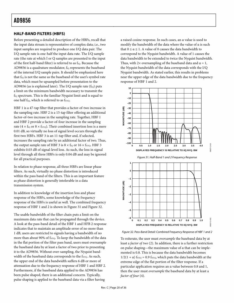
In addition to knowledge of the insertion loss and phase response of the HBFs, some knowledge of the frequency response of the HBFs is useful as well. The combined frequency response of HBF 1 and 2 is shown in Figure 31 and Figure 32.
The usable bandwidth of the filter chain puts a limit on the maximum data rate that can be propagated through the device. A look at the pass-band detail of the HBF 1 and HFB 2 response indicates that to maintain an amplitude error of no more than 1 dB, users are restricted to signals having a bandwidth of no more than about 90% of fNYQ. To keep the bandwidth of the data in the flat portion of the filter pass band, users must oversample the baseband data by at least a factor of two prior to presenting it to the AD9856. Without over-sampling, the Nyquist band-width of the baseband data corresponds to the fNYQ. As such, the upper end of the data bandwidth suffers 6 dB or more of attenuation due to the frequency response of HBF 1 and HBF 2. Furthermore, if the baseband data applied to the AD9856 has been pulse shaped, there is an additional concern. Typically, pulse shaping is applied to the baseband data via a filter having
a raised cosine response. In such cases, an α value is used to modify the bandwidth of the data where the value of α is such that 0 ≤ α ≤ 1. A value of 0 causes the data bandwidth to correspond to the Nyquist bandwidth. A value of 1 causes the data bandwidth to be extended to twice the Nyquist bandwidth. Thus, with 2× oversampling of the baseband data and α = 1, the Nyquist bandwidth of the data corresponds with the I/Q Nyquist bandwidth. As stated earlier, this results in problems near the upper edge of the data bandwidth due to the frequency response of HBF 1 and 2.
–100
–90
–70
–30
–10
10
–50
–80
–40
–20
0
–60MA
GN
ITU
DE
(dB
)
2.01.50.5 1.00 2.5 3.0 3.5 4.0
DISPLAYED FREQUENCY IS RELATIVE TO I/Q NYQ. BW 0063
7-C
-031
Figure 31. Half-Band 1 and 2 Frequency Response
–6
–5
–4
–3
–2
–1
0
1
MA
GN
ITU
DE
(dB
)
0 0.1 0.2 0.3 0.4 0.5 0.6 0.7 0.8 0.9 1.0
DISPLAYED FREQUENCY IS RELATIVE TO I/Q NYQ. BW 0063
7-C
-032
Figure 32. Pass-Band Detail: Combined Frequency Response of HBF 1 and 2
To reiterate, the user must oversample the baseband data by at least a factor of two (2). In addition, there is a further restriction on pulse shaping—the maximum value of α that can be imple-mented is 0.8. This is because the data bandwidth becomes 1/2(1 + α) fNYQ = 0.9 fNYQ, which puts the data bandwidth at the extreme edge of the flat portion of the filter response. If a particular application requires an α value between 0.8 and 1, then the user must oversample the baseband data by at least a factor of four (4).
AD9856
Rev. C | Page 21 of 36
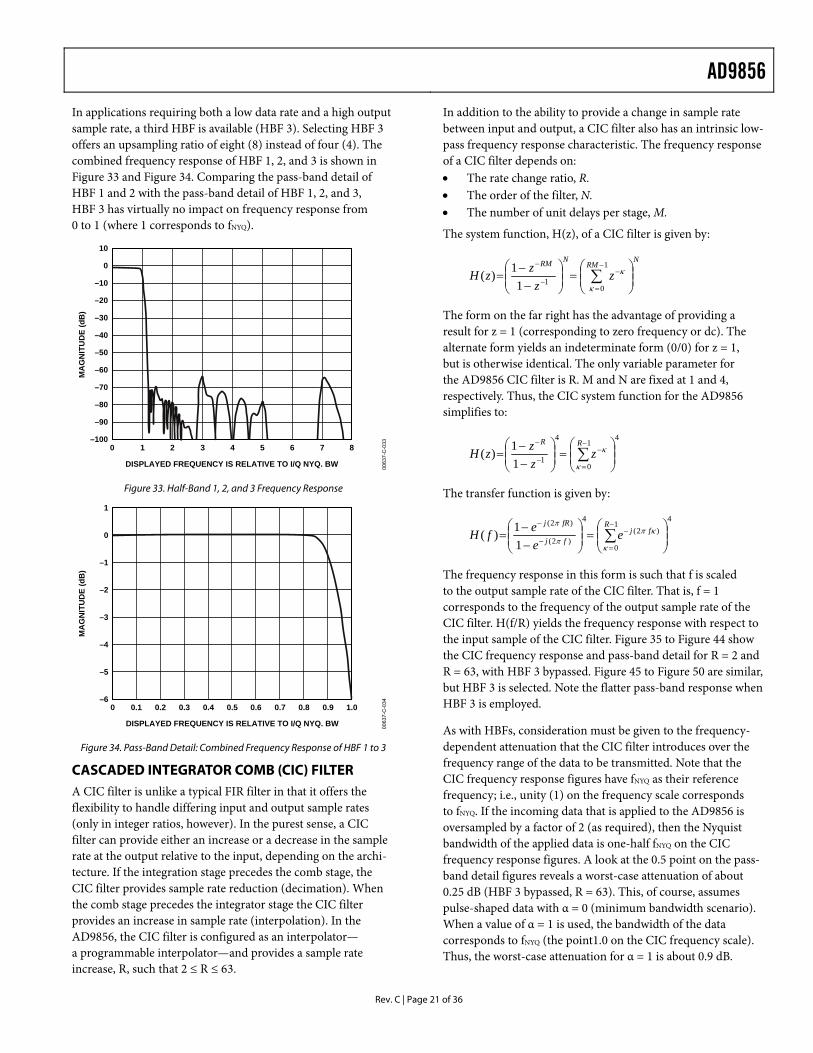
In applications requiring both a low data rate and a high output sample rate, a third HBF is available (HBF 3). Selecting HBF 3 offers an upsampling ratio of eight (8) instead of four (4). The combined frequency response of HBF 1, 2, and 3 is shown in Figure 33 and Figure 34. Comparing the pass-band detail of HBF 1 and 2 with the pass-band detail of HBF 1, 2, and 3, HBF 3 has virtually no impact on frequency response from 0 to 1 (where 1 corresponds to fNYQ).
–100
–90
–70
–30
–10
10
–50
–80
–40
–20
0
–60MA
GN
ITU
DE
(dB
)
431 20 5
DISPLAYED FREQUENCY IS RELATIVE TO I/Q NYQ. BW
6 7 8
0063
7-C
-033
Figure 33. Half-Band 1, 2, and 3 Frequency Response
–6
–5
–4
–3
–2
–1
0
1
MA
GN
ITU
DE
(dB
)
0 0.1 0.2 0.3 0.4 0.5 0.6 0.7 0.8 0.9 1.0
DISPLAYED FREQUENCY IS RELATIVE TO I/Q NYQ. BW 0063
7-C
-034
Figure 34. Pass-Band Detail: Combined Frequency Response of HBF 1 to 3
CASCADED INTEGRATOR COMB (CIC) FILTER A CIC filter is unlike a typical FIR filter in that it offers the flexibility to handle differing input and output sample rates (only in integer ratios, however). In the purest sense, a CIC filter can provide either an increase or a decrease in the sample rate at the output relative to the input, depending on the archi-tecture. If the integration stage precedes the comb stage, the CIC filter provides sample rate reduction (decimation). When the comb stage precedes the integrator stage the CIC filter provides an increase in sample rate (interpolation). In the AD9856, the CIC filter is configured as an interpolator— a programmable interpolator—and provides a sample rate increase, R, such that 2 ≤ R ≤ 63.
In addition to the ability to provide a change in sample rate between input and output, a CIC filter also has an intrinsic low-pass frequency response characteristic. The frequency response of a CIC filter depends on: • The rate change ratio, R. • The order of the filter, N. • The number of unit delays per stage, M.
The system function, H(z), of a CIC filter is given by:
NRM
NRM
zz
zzH ⎟⎟⎠
⎞⎜⎜⎝
⎛=⎟⎟
⎠
⎞⎜⎜⎝
⎛
−−
= ∑−
=
−−
− 1
011
1)(κ
κ
The form on the far right has the advantage of providing a result for z = 1 (corresponding to zero frequency or dc). The alternate form yields an indeterminate form (0/0) for z = 1, but is otherwise identical. The only variable parameter for the AD9856 CIC filter is R. M and N are fixed at 1 and 4, respectively. Thus, the CIC system function for the AD9856 simplifies to:
41
0
4
111)( ⎟⎟
⎠
⎞⎜⎜⎝
⎛=⎟⎟
⎠
⎞⎜⎜⎝
⎛
−−
= ∑−
=
−−
− RR
zzzzH
κ
κ
The transfer function is given by:
41
0
)2(4
)2(
)2(
11)( ⎟⎟
⎠
⎞⎜⎜⎝
⎛=⎟⎟
⎠
⎞⎜⎜⎝
⎛
−−
= ∑−
=
−−
− Rfj
fj
fRj
eeefH
κ
κππ
π
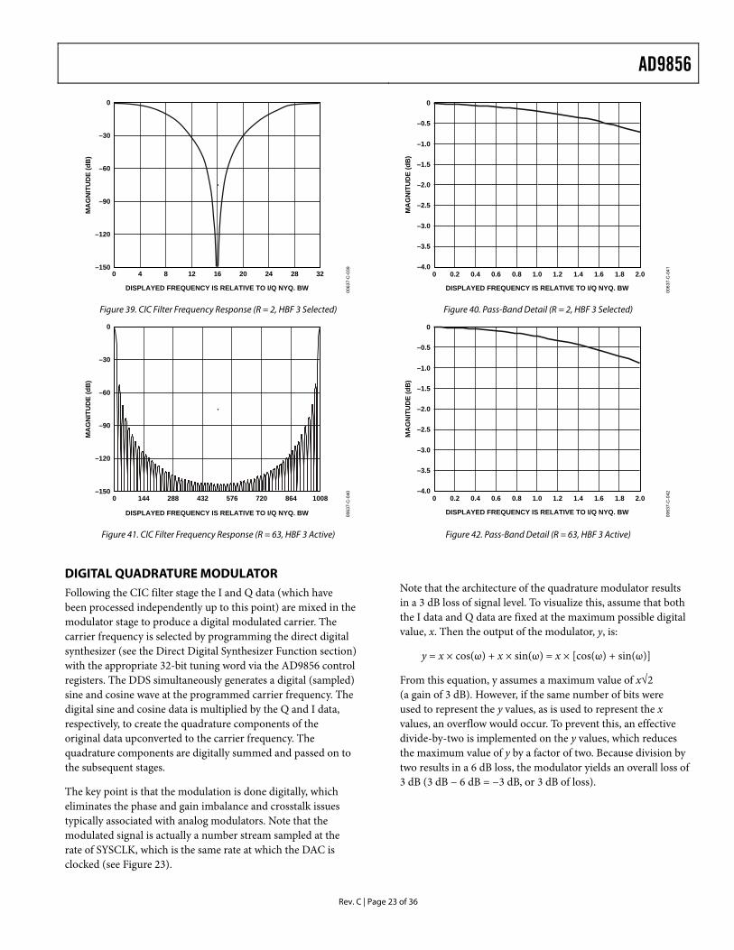
The frequency response in this form is such that f is scaled to the output sample rate of the CIC filter. That is, f = 1 corresponds to the frequency of the output sample rate of the CIC filter. H(f/R) yields the frequency response with respect to the input sample of the CIC filter. Figure 35 to Figure 44 show the CIC frequency response and pass-band detail for R = 2 and R = 63, with HBF 3 bypassed. Figure 45 to Figure 50 are similar, but HBF 3 is selected. Note the flatter pass-band response when HBF 3 is employed.
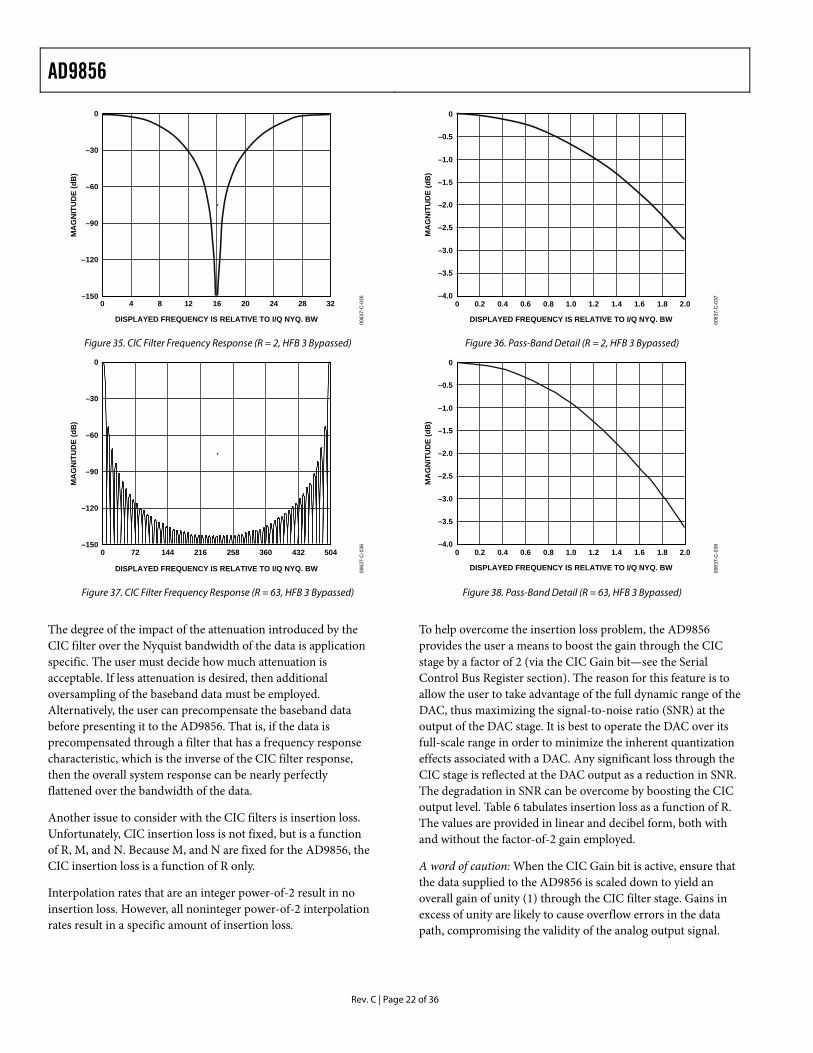
As with HBFs, consideration must be given to the frequency-dependent attenuation that the CIC filter introduces over the frequency range of the data to be transmitted. Note that the CIC frequency response figures have fNYQ as their reference frequency; i.e., unity (1) on the frequency scale corresponds to fNYQ. If the incoming data that is applied to the AD9856 is oversampled by a factor of 2 (as required), then the Nyquist bandwidth of the applied data is one-half fNYQ on the CIC frequency response figures. A look at the 0.5 point on the pass-band detail figures reveals a worst-case attenuation of about 0.25 dB (HBF 3 bypassed, R = 63). This, of course, assumes pulse-shaped data with α = 0 (minimum bandwidth scenario). When a value of α = 1 is used, the bandwidth of the data corresponds to fNYQ (the point1.0 on the CIC frequency scale). Thus, the worst-case attenuation for α = 1 is about 0.9 dB.
AD9856
Rev. C | Page 22 of 36
–150
–120
–90
–60
–30
0
MA
GN
ITU
DE
(dB
)
16124 80 20 24 2
DISPLAYED FREQUENCY IS RELATIVE TO I/Q NYQ. BW 0063
7-C
-0358 32
–4.0
–3.5
–3.0
–2.5
–2.0
–1.5
MA
GN
ITU
DE
(dB
)
–1.0
–0.5
0
0 0.2 0.4 0.6 0.8 1.0 1.2 1.4 1.6 1.8 2.0
DISPLAYED FREQUENCY IS RELATIVE TO I/Q NYQ. BW 0063
7-C
-037
Figure 35. CIC Filter Frequency Response (R = 2, HFB 3 Bypassed) Figure 36. Pass-Band Detail (R = 2, HFB 3 Bypassed)
–150
–120
–90
–60
–30
0
MA
GN
ITU
DE
(dB
)
0 72 144 216 258 360 432 504
DISPLAYED FREQUENCY IS RELATIVE TO I/Q NYQ. BW 0063
7-C
-036
–4.0
–3.5
–3.0
–2.5
–2.0
–1.5M
AG
NIT
UD
E (d
B)
–1.0
–0.5
0
0 0.2 0.4 0.6 0.8 1.0 1.2 1.4 1.6 1.8 2.0
DISPLAYED FREQUENCY IS RELATIVE TO I/Q NYQ. BW 0063
7-C
-038
Figure 37. CIC Filter Frequency Response (R = 63, HFB 3 Bypassed) Figure 38. Pass-Band Detail (R = 63, HFB 3 Bypassed)
The degree of the impact of the attenuation introduced by the CIC filter over the Nyquist bandwidth of the data is application specific. The user must decide how much attenuation is acceptable. If less attenuation is desired, then additional oversampling of the baseband data must be employed. Alternatively, the user can precompensate the baseband data before presenting it to the AD9856. That is, if the data is precompensated through a filter that has a frequency response characteristic, which is the inverse of the CIC filter response, then the overall system response can be nearly perfectly flattened over the bandwidth of the data.
Another issue to consider with the CIC filters is insertion loss. Unfortunately, CIC insertion loss is not fixed, but is a function of R, M, and N. Because M, and N are fixed for the AD9856, the CIC insertion loss is a function of R only.
Interpolation rates that are an integer power-of-2 result in no insertion loss. However, all noninteger power-of-2 interpolation rates result in a specific amount of insertion loss.
To help overcome the insertion loss problem, the AD9856 provides the user a means to boost the gain through the CIC stage by a factor of 2 (via the CIC Gain bit—see the Serial Control Bus Register section). The reason for this feature is to allow the user to take advantage of the full dynamic range of the DAC, thus maximizing the signal-to-noise ratio (SNR) at the output of the DAC stage. It is best to operate the DAC over its full-scale range in order to minimize the inherent quantization effects associated with a DAC. Any significant loss through the CIC stage is reflected at the DAC output as a reduction in SNR. The degradation in SNR can be overcome by boosting the CIC output level. Table 6 tabulates insertion loss as a function of R. The values are provided in linear and decibel form, both with and without the factor-of-2 gain employed.
A word of caution: When the CIC Gain bit is active, ensure that the data supplied to the AD9856 is scaled down to yield an overall gain of unity (1) through the CIC filter stage. Gains in excess of unity are likely to cause overflow errors in the data path, compromising the validity of the analog output signal.
AD9856
Rev. C | Page 23 of 36
–150
–120
–90
–60
–30
0
MA
GN
ITU
DE
(dB
)
16124 80 20 24 2
DISPLAYED FREQUENCY IS RELATIVE TO I/Q NYQ. BW 0063
7-C
-0398 32
–4.0
–3.5
–3.0
–2.5
–2.0
–1.5
MA
GN
ITU
DE
(dB
)
–1.0
–0.5
0
0 0.2 0.4 0.6 0.8 1.0 1.2 1.4 1.6 1.8 2.0
DISPLAYED FREQUENCY IS RELATIVE TO I/Q NYQ. BW 0063
7-C
-041
Figure 39. CIC Filter Frequency Response (R = 2, HBF 3 Selected) Figure 40. Pass-Band Detail (R = 2, HBF 3 Selected)
–150
–120
–90
–60
–30
0
MA
GN
ITU
DE
(dB
)
0 144 288 432 576 720 864 1008
DISPLAYED FREQUENCY IS RELATIVE TO I/Q NYQ. BW 0063
7-C
-040
–4.0
–3.5
–3.0
–2.5
–2.0
–1.5
MA
GN
ITU
DE
(dB
)
–1.0
–0.5
0
0 0.2 0.4 0.6 0.8 1.0 1.2 1.4 1.6 1.8 2.0
DISPLAYED FREQUENCY IS RELATIVE TO I/Q NYQ. BW 0063
7-C
-042
Figure 41. CIC Filter Frequency Response (R = 63, HBF 3 Active) Figure 42. Pass-Band Detail (R = 63, HBF 3 Active)
DIGITAL QUADRATURE MODULATOR Following the CIC filter stage the I and Q data (which have been processed independently up to this point) are mixed in the modulator stage to produce a digital modulated carrier. The carrier frequency is selected by programming the direct digital synthesizer (see the Direct Digital Synthesizer Function section) with the appropriate 32-bit tuning word via the AD9856 control registers. The DDS simultaneously generates a digital (sampled) sine and cosine wave at the programmed carrier frequency. The digital sine and cosine data is multiplied by the Q and I data, respectively, to create the quadrature components of the original data upconverted to the carrier frequency. The quadrature components are digitally summed and passed on to the subsequent stages.
The key point is that the modulation is done digitally, which eliminates the phase and gain imbalance and crosstalk issues typically associated with analog modulators. Note that the modulated signal is actually a number stream sampled at the rate of SYSCLK, which is the same rate at which the DAC is clocked (see Figure 23).
Note that the architecture of the quadrature modulator results in a 3 dB loss of signal level. To visualize this, assume that both the I data and Q data are fixed at the maximum possible digital value, x. Then the output of the modulator, y, is:
y = x × cos(ω) + x × sin(ω) = x × [cos(ω) + sin(ω)]
From this equation, y assumes a maximum value of x√2 (a gain of 3 dB). However, if the same number of bits were used to represent the y values, as is used to represent the x values, an overflow would occur. To prevent this, an effective divide-by-two is implemented on the y values, which reduces the maximum value of y by a factor of two. Because division by two results in a 6 dB loss, the modulator yields an overall loss of 3 dB (3 dB − 6 dB = −3 dB, or 3 dB of loss).
AD9856
Rev. C | Page 24 of 36
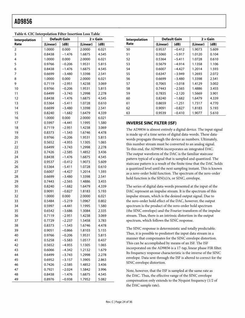
Table 6. CIC Interpolation Filter Insertion Loss Table Default Gain 2 × Gain Interpolation
Rate (Linear) (dB) (Linear) (dB) 2 1.0000 0.000 2.0000 6.021 3 0.8438 −1.476 1.6875 4.545 4 1.0000 0.000 2.0000 6.021 5 0.9766 −0.206 1.9531 5.815 6 0.8438 −1.476 1.6875 4.545 7 0.6699 −3.480 1.3398 2.541 8 1.0000 0.000 2.0000 6.021 9 0.7119 −2.951 1.4238 3.069 10 0.9766 −0.206 1.9531 5.815 11 0.6499 −3.743 1.2998 2.278 12 0.8438 −1.476 1.6875 4.545 13 0.5364 −5.411 1.0728 0.610 14 0.6699 −3.480 1.3398 2.541 15 0.8240 −1.682 1.6479 4.339 16 1.0000 0.000 2.0000 6.021 17 0.5997 −4.441 1.1995 1.580 18 0.7119 −2.951 1.4238 3.069 19 0.8373 −1.543 1.6746 4.478 20 0.9766 −0.206 1.9531 5.815 21 0.5652 −4.955 1.1305 1.065 22 0.6499 −3.743 1.2998 2.278 23 0.7426 −2.585 1.4852 3.436 24 0.8438 −1.476 1.6875 4.545 25 0.9537 −0.412 1.9073 5.609 26 0.5364 −5.411 1.0728 0.610 27 0.6007 −4.427 1.2014 1.593 28 0.6699 −3.480 1.3398 2.541 29 0.7443 −2.565 1.4886 3.455 30 0.8240 −1.682 1.6479 4.339 31 0.9091 −0.827 1.8183 5.193 32 1.0000 0.000 2.0000 6.021 33 0.5484 −5.219 1.0967 0.802 34 0.5997 −4.441 1.1995 1.580 35 0.6542 −3.686 1.3084 2.335 36 0.7119 −2.951 1.4238 3.069 37 0.7729 −2.237 1.5458 3.783 38 0.8373 −1.543 1.6746 4.478 39 0.9051 −0.866 1.8103 5.155 40 0.9766 −0.206 1.9531 5.815 41 0.5258 −5.583 1.0517 0.437 42 0.5652 −4.955 1.1305 1.065 43 0.6066 −4.342 1.2132 1.679 44 0.6499 −3.743 1.2998 2.278 45 0.6952 −3.157 1.3905 2.863 46 0.7426 −2.585 1.4852 3.436 47 0.7921 −2.024 1.5842 3.996 48 0.8438 −1.476 1.6875 4.545 49 0.8976 −0.938 1.7952 5.082
Default Gain 2 × Gain Interpolation Rate (Linear) (dB) (Linear) (dB) 50 0.9537 −0.412 1.9073 5.609 51 0.5060 −5.917 1.0120 0.104 52 0.5364 −5.411 1.0728 0.610 53 0.5679 −4.914 1.1358 1.106 54 0.6007 −4.427 1.2014 1.593 55 0.6347 −3.949 1.2693 2.072 56 0.6699 −3.480 1.3398 2.541 57 0.7065 −3.018 1.4129 3.002 58 0.7443 −2.565 1.4886 3.455 59 0.7835 −2.120 1.5669 3.901 60 0.8240 −1.682 1.6479 4.339 61 0.8659 −1.251 1.7317 4.770 62 0.9091 −0.827 1.8183 5.193 63 0.9539 −0.410 1.9077 5.610
INVERSE SINC FILTER (ISF) The AD9856 is almost entirely a digital device. The input signal is made up of a time series of digital data-words. These data-words propagate through the device as numbers. Ultimately, this number stream must be converted to an analog signal. To this end, the AD9856 incorporates an integrated DAC. The output waveform of the DAC is the familiar staircase pattern typical of a signal that is sampled and quantized. The staircase pattern is a result of the finite time that the DAC holds a quantized level until the next sampling instant. This is known as a zero-order hold function. The spectrum of the zero-order hold function is the SIN(x)/x, or SINC, envelope.
The series of digital data-words presented at the input of the DAC represent an impulse stream. It is the spectrum of this impulse stream, which is the desired output signal. Due to the zero-order hold effect of the DAC, however, the output spectrum is the product of the zero-order hold spectrum (the SINC envelope) and the Fourier transform of the impulse stream. Thus, there is an intrinsic distortion in the output spectrum, which follows the SINC response.
The SINC response is deterministic and totally predictable. Thus, it is possible to predistort the input data stream in a manner that compensates for the SINC envelope distortion. This can be accomplished by means of an ISF. The ISF incorporated on the AD9856 is a 17-tap, linear phase FIR filter. Its frequency response characteristic is the inverse of the SINC envelope. Data sent through the ISF is altered to correct for the SINC envelope distortion.
Note, however, that the ISF is sampled at the same rate as the DAC. Thus, the effective range of the SINC envelope compensation only extends to the Nyquist frequency (1/2 of the DAC sample rate).

AD9856
Rev. C | Page 25 of 36
Figure 43 shows the effectiveness of the ISF in correcting for the SINC distortion. The plot includes a graph of the SINC envelope, the ISF response and the SYSTEM response (which is the product of the SINC and ISF responses). Note that the ISF exhibits an insertion loss of 3.1 dB. Thus, signal levels at the output of the AD9856 with the ISF bypassed are 3.1 dB higher than with the ISF engaged. For modulated output signals, however, which have a relatively wide bandwidth, the benefits of the SINC compensation usually outweigh the 3 dB loss in output level. The decision of whether to use the ISF is an application specific system design issue.
–4
–3
–2
–1
0
1
(dB
)
2
3
4
0 0.1 0.2 0.3 0.4 0.5
FREQUENCY NORMALIZED TO SAMPLE RATE
ISF
SINC
SYSTEM00
637-
C-0
43
Figure 43. Inverse SINC Filter Response
DIRECT DIGITAL SYNTHESIZER FUNCTION The direct digital synthesizer (DDS) block generates the sine/ cosine carrier reference signals that are digitally modulated by the I/Q data paths. The DDS function is frequency tuned via the serial control port with a 32-bit tuning word. This allows the AD9856’s output carrier frequency to be very precisely tuned while still providing output frequency agility.
The equation relating output frequency of the AD9856 digital modulator to the frequency tuning word (FTWORD) and the system clock (SYSCLK) is given as:
( ) 322/SYSCLKFTWORDAOUT ×=
where AOUT and SYSCLK frequencies are in Hz and FTWORD is a decimal number from 0 to 4,294,967,296 (231).
For example, find the FTWORD for AOUT = 41 MHz and SYSCLK = 122.88 MHz.
If AOUT = 41 MHz and SYSCLK = 122.88 MHz, then:
hexAAAABFTWORD 556=
Loading 556AAAABh into control bus registers 02h–05h (for Profile 1) programs the AD9856 for AOUT = 41 MHz, given a SYSCLK frequency of 122.88 MHz.
A Technical Tutorial on Digital Signal Synthesis is available on the Analog Devices website at: http://www.analog.com/UploadedFiles/Tutorials/450968421DDS_Tutorial_rev12-2-99.pdf
The tutorial provides basic applications information for a variety of digital synthesis implementations, as well as a detailed explanation of aliases.
D/A CONVERTER A 12-bit digital-to-analog converter (DAC) is used to convert the digitally processed waveform into an analog signal. The worst-case spurious signals due to the DAC are the harmonics of the fundamental signal and their aliases (see the AD9851 Complete-DDS data sheet for a details about aliased images). The wideband 12-bit DAC in the AD9856 maintains spurious-free dynamic range (SFDR) performance of −60 dBc up to AOUT = 42 MHz and −55 dBc up to AOUT = 65 MHz.
The conversion process produces aliased components of the fundamental signal at n × SYSCLK ± FCARRIER (n = 1, 2, 3). These are typically filtered with an external RLC filter at the DAC output. It is important for this analog filter to have a sufficiently flat gain and linear phase response across the bandwidth of interest to avoid modulation impairments. An inexpensive seventh-order elliptical low-pass filter is sufficient to suppress the aliased components for HFC network applications.
The AD9856 provides true and complement current outputs on pins 30 and 29, respectively. The full-scale output current is set by the RSET resistor at Pin 25. The value of RSET for a particular IOUT is determined by
OUTSET IR 39.936/=
For example, if a full-scale output current of 20 mA is desired, then RSET = (39.936/0.02), or approximately 2 kΩ. Every doubling of the RSET value halves the output current. Maximum output current is specified as 20 mA.
The full-scale output current range of the AD9856 is 5 mA to 20 mA. Full-scale output currents outside of this range degrade SFDR performance. SFDR is also slightly affected by output matching, that is, the two outputs should be terminated equally for best SFDR performance.
The output load should be located as close as possible to the AD9856 package to minimize stray capacitance and inductance. The load may be a simple resistor to ground, an op amp current-to-voltage converter, or a transformer-coupled circuit. It is best not to attempt to directly drive highly reactive loads (such as an LC filter). Driving an LC filter without a transformer requires that the filter be doubly terminated for best performance, that is, the filter input and output should both be resistively terminated with the appropriate values. The parallel combination of the two terminations determines the
AD9856
Rev. C | Page 26 of 36
load that the AD9856 sees for signals within the filter pass band. For example, a 50 Ω terminated input/output low-pass filter looks like a 25 Ω load to the AD9856.
The output compliance voltage of the AD9856 is −0.5 V to +1.5 V. Any signal developed at the DAC output should not exceed +1.5 V, otherwise, signal distortion results. Furthermore, the signal may extend below ground as much as 0.5 V without damage or signal distortion. The use of a transformer with a grounded center tap for common-mode rejection results in signals at the AD9856 DAC output pins that are symmetrical about ground.
As previously mentioned, by differentially combining the two signals the user can provide some degree of common-mode signal rejection. A differential combiner might consist of a transformer or an op amp. The object is to combine or amplify only the difference between two signals and to reject any common, usually undesirable, characteristic, such as 60 Hz hum or clock feedthrough that is equally present on both input signals. The AD9856 true and complement outputs can be differentially combined using a broadband 1:1 transformer with a grounded, center-tapped primary to perform differential combining of the two DAC outputs.
REFERENCE CLOCK MULTIPLIER Because the AD9856 is a DDS-based modulator, a relatively high frequency system clock is required. For DDS applications, the carrier is typically limited to about 40% of SYSCLK. For a 65 MHz carrier, the system clock required is above 160 MHz. To avoid the cost associated with these high frequency references and the noise coupling issues associated with operating a high frequency clock on a PC board, the AD9856 provides an on-chip programmable clock multiplier (REFCLK multiplier). The available clock multiplier range is from 4× to 20×, in integer steps. With the REFCLK multiplier enabled, the input reference clock required for the AD9856 can be kept in the 10 MHz to 50 MHz range for 200 MHz system operation, which results in cost and system implementation savings. The REFCLK mult-iplier function maintains clock integrity as evidenced by the AD9856’s system phase noise characteristics of −105 dBc/Hz (AOUT = 40 MHz, REFCLK multiplier = 6, Offset = 1 kHz) and virtually no clock related spurii in the output spectrum. External loop filter components consisting of a series resistor (1.3 kΩ) and capacitor (0.01 µF) provide the compensation zero for the REFCLK multiplier PLL loop. The overall loop perform-ance has been optimized for these component values.
THROUGHPUT AND LATENCY Data latency through the AD9856 is easiest to describe in terms of SYSCLK clock cycles. Latency is a function of the AD9856 configuration primarily affected by the CIC interpolation rate and whether the third half-band filter is engaged.
When the third half-band filter is engaged, the AD9856 latency is given by 126 N + 37 SYSCLK clock cycles, where N is the CIC interpolation rate.
If the AD9856 is configured to bypass the third half-band filter, the latency is given by 63 N + 37 SYSCLK clock cycles.
These equations should be considered estimates, as observed latency may be data dependent. The latency was calculated using the linear delay model for the FIR filters.
In single-tone mode, frequency hopping is accomplished via changing the PROFILE input pins. The time required to switch from one frequency to another is < 50 SYSCLK cycles with the inverse SINC filter engaged. With the inverse SINC filter bypassed, the latency drops to < 35 SYSCLK cycles.
CONTROL INTERFACE The flexible AD9856 synchronous serial communications port allows easy interface to many industry standard micro-controllers and microprocessors. The serial I/O is compatible with most synchronous transfer formats, including the Motorola 6905/11 SPI® and Intel® 8051 SSR protocols.
The interface allows read/write access to all registers that configure the AD9856. Single or multiple byte transfers are supported, as well as MSB first or LSB first transfer formats. The AD9856’s serial interface port can be configured as a single-pin I/O (SDIO) or two unidirectional pins for input/output (SDIO/SDO).
GENERAL OPERATION OF THE SERIAL INTERFACE There are two phases to a communication cycle with the AD9856. Phase 1 is the instruction cycle, which is the writing of an instruction byte into the AD9856, coincident with the first eight SCLK rising edges. The instruction byte provides the AD9856 serial port controller with information regarding the data transfer cycle, which is Phase 2 of the communication cycle. The Phase 1 instruction byte defines whether the upcoming data transfer is read or write, the number of bytes in the data transfer (1 to 4), and the starting register address for the first byte of the data transfer.
The first eight SCLK rising edges of each communication cycle are used to write the instruction byte into the AD9856. The remaining SCLK edges are for Phase 2 of the communication cycle. Phase 2 is the actual data transfer between the AD9856 and the system controller. Phase 2 of the communication cycle is a transfer of 1, 2, 3, or 4 data bytes as determined by the instruction byte. Normally, using one communication cycle in a multibyte transfer is the preferred method. However, single-byte communication cycles are useful to reduce CPU overhead when register access requires one byte only. Examples of this may be to write the AD9856 SLEEP bit, or an AD8320/AD8321 gain control byte.
AD9856
Rev. C | Page 27 of 36
At the completion of any communication cycle, the AD9856 serial port controller expects the next eight rising SCLK edges to be the instruction byte of the next communication cycle.
All data input to the AD9856 is registered on the rising edge of SCLK. All data is driven out of the AD9856 on the falling edge of SCLK. Figure 44 through Figure 47 show the general operation of the AD9856 serial port.
INSTRUCTION BYTE The instruction byte contains the following information as shown in Table 7.
Table 7. Instruction Byte Information MSB D6 D5 D4 D3 D2 D1 LSB R/W N1 N0 A4 A3 A2 A1 A0
R/W—Bit 7 determines whether a read or write data transfer occurs after the instruction byte write. Logic high indicates a read operation. Logic zero indicates a write operation.
N1, N0—Bits 6 and 5 of the instruction byte determine the number of bytes to be transferred during the data transfer cycle of the communications cycle. Table 8 shows the decode bits.
Table 8. N1, N0 Decode Bits N1 N0 Description 0 0 Transfer 1 byte 0 1 Transfer 2 bytes 1 0 Transfer 3 bytes 1 1 Transfer 4 bytes
A4, A3, A2, A1, A0—Bits 4, 3, 2, 1, 0 of the instruction byte determine which register is accessed during the data transfer portion of the communications cycle. For multibyte transfers, this address is the starting byte address. The remaining register addresses are generated by the AD9856.
I7SDIO
INSTRUCTION CYCLE DATA TRANSFER CYCLE
SCLK
CS
I6 I5 I4 I3 I2 I1 I0 D7 D6 D5 D4 D3 D2 D1 D0
0063
7-C
-044
Figure 44. Serial Port Writing Timing—Clock Stall Low
DO 7
INSTRUCTION CYCLE DATA TRANSFER CYCLE
DON'T CAREI7 I6 I5 I4 I3 I2 I1 I0SDIO
SCLK
CS
SDO DO 6 DO 5 DO 4 DO 3 DO 2 DO 1 DO 000
637-
C-0
45
Figure 45. Three-Wire Serial Port Read Timing—Clock Stall Low
I7SDIO
INSTRUCTION CYCLE DATA TRANSFER CYCLE
SCLK
CS
I6 I5 I4 I3 I2 I1 I0 D7 D6 D5 D4 D3 D2 D1 D0
0063
7-C
-046
Figure 46. Serial Port Write Timing—Clock Stall High
I7SDIO
INSTRUCTION CYCLE DATA TRANSFER CYCLE
SCLK
CS
I6 I5 I4 I3 I2 I1 I0 DO 7 DO 6 DO 5 DO 4 DO 3 DO 2 DO 1 DO 0
0063
7-C
-047
Figure 47. Two-Wire Serial Port Read Timing—Clock Stall High
AD9856
Rev. C | Page 28 of 36
SERIAL INTERFACE PORT PIN DESCRIPTIONS
SCLK—Serial Clock
The serial clock pin is used to synchronize data to and from the AD9856 and to run the internal state machines. SCLK maximum frequency is 10 MHz.
CS—Chip Select Active low input that allows more than one device on the same serial communications lines. The SDO and SDIO pins go to a high impedance state when this input is high. If driven high during any communications cycle, that cycle is suspended until CS is reactivated low. Chip Select can be tied low in systems that maintain control of SCLK.
SDIO—Serial Data I/O Data is always written into the AD9856 on this pin. However, this pin can be used as a bidirectional data line. The config-uration of this pin is controlled by Bit 7 of register address 0h. The default is Logic 0, which configures the SDIO pin as bidirectional.
SDO—Serial Data Out Data is read from this pin for protocols that use separate lines for transmitting and receiving data. In the case where the AD9856 operates in a single bidirectional I/O mode, this pin does not output data and is set to a high impedance state.
SYNC I/O Synchronizes the I/O port state machines without affecting the addressable registers contents. An active high input on the SYNC I/O pin causes the current communication cycle to abort. After SYNC I/O returns low (Logic 0), another communication cycle may begin, starting with the instruction byte write.
CA CLK Output clock pin to the AD8320/AD8321. If using the AD9856 to control the AD8320/AD8321 programmable cable driver amplifier, connect this pin to the CLK input of the AD8320/ AD8321.
CA DATA Output data pin to the AD8320/AD8321. If using the AD9856 to control the AD8320/AD8321 programmable cable driver amplifier, connect this pin to the SDATA input of the AD8320/ AD8321.
CA ENABLE Output Enable pin to the AD8320/AD8321. If using the AD9856 to control the AD8320/AD8321 programmable cable driver amplifier, connect this pin to the DATEN input of the AD8320/AD8321.
MSB/LSB TRANSFERS The AD9856 serial port can support both MSB-first or LSB-first data formats. This functionality is controlled by the REG0<6> bit. The default value of REG0<6> is low (MSB first). When
REG0<6> is set active high, the AD9856 serial port is in LSB first format. The instruction byte must be written in the format indicated by REG0<6>. That is, if the AD9856 is in LSB-first mode, the instruction byte must be written from least significant bit to most significant bit. Multibyte data transfers in MSB format can be completed by writing an instruction byte that includes the register address of the most significant byte. In MSB-first mode, the serial port internal byte address generator decrements for each byte required of the multibyte commun-ication cycle. Multibyte data transfers in LSB-first format can be completed by writing an instruction byte that includes the register address of the least significant byte. In LSB-first mode, the serial port internal byte address generator increments for each byte required of the multibyte communication cycle.
NOTES ON SERIAL PORT OPERATION The AD9856 serial port configuration bits reside in Bit 6 and Bit 7 of register address 0h. It is important to note that the configuration changes immediately upon writing to this register. For multibyte transfers, writing to this register may occur during the middle of a communication cycle. Care must be taken to compensate for this new configuration for the remainder of the current communication cycle.
The AD9856 serial port controller address can roll from 19h to 0h for multibyte I/O operations if the MSB-first mode is active. The serial port controller address can roll from 0h to 19h for multibyte I/O operations if the LSB-first mode is active.
The system must maintain synchronization with the AD9856 or the internal control logic is not able to recognize further instructions. For example, if the system sends an instruction byte for a 2-byte write, then pulses the SCLK pin for a 3-byte write (24 additional SCLK rising edges), communication synchronization is lost. In this case, the first 16 SCLK rising edges after the instruction cycle properly write the first two data bytes into the AD9856, but the next eight rising SCLK edges are interpreted as the next instruction byte, not the final byte of the previous communication cycle.
In the case where synchronization is lost between the system and the AD9856, the SYNC I/O pin provides a means to reestablish synchronization without reinitializing the entire chip. The SYNC I/O pin enables the user to reset the AD9856 state machine to accept the next eight SCLK rising edges to be coincident with the instruction phase of a new communication cycle. By applying and removing a high signal to the SYNC I/O pin, the AD9856 is set to once again begin performing the communication cycle in synchronization with the system. Any information that had been written to the AD9856 registers during a valid communication cycle prior to loss of synchronization remains intact.
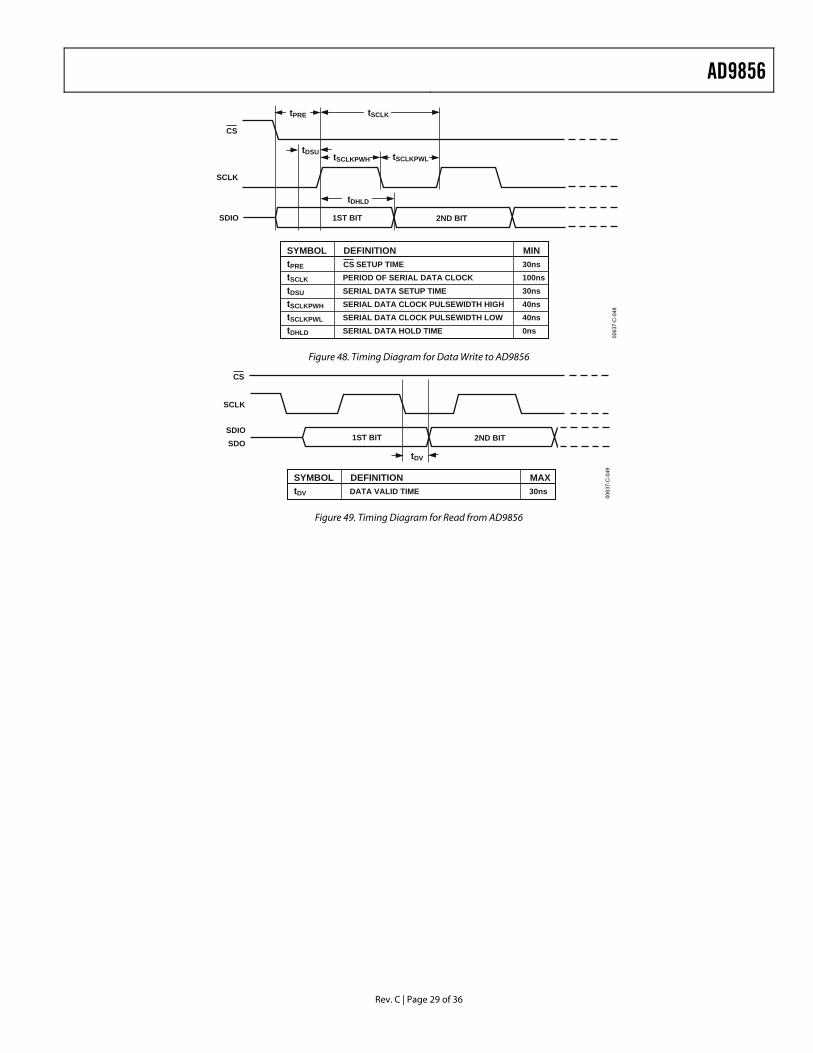
AD9856
Rev. C | Page 29 of 36
SYMBOL DEFINITION MINtPRE SETUP TIME 30nstSCLK PERIOD OF SERIAL DATA CLOCK 100nstDSU SERIAL DATA SETUP TIME 30nstSCLKPWH SERIAL DATA CLOCK PULSEWIDTH HIGH 40nstSCLKPWL SERIAL DATA CLOCK PULSEWIDTH LOW 40nstDHLD SERIAL DATA HOLD TIME 0ns
CS
SCLK
SDIO 1ST BIT 2ND BIT
tDSU
tDHLD
tSCLKPWH tSCLKPWL
tSCLKtPRE
CS
0063
7-C
-048
Figure 48. Timing Diagram for Data Write to AD9856
SYMBOL DEFINITION MAXtDV DATA VALID TIME 30ns
CS
SCLK
SDIO1ST BIT 2ND BIT
tDV
SDO
0063
7-C
-049
Figure 49. Timing Diagram for Read from AD9856

AD9856
Rev. C | Page 30 of 36
PROGRAMMING/WRITING THE AD8320/AD8321 CABLE DRIVER AMPLIFIER GAIN CONTROL Programming the gain control register of the AD8320/AD8321 programmable cable driver amplifier can be accomplished via the AD9856 serial port. Four 8-bit registers (one per profile) within the AD9856 store the gain value to be written to the AD8320/AD8321. The AD8320/AD8321 is written via three dedicated AD9856 output pins that are directly connected to the AD8320/AD8321 serial input port. The transfer of data from the AD9856 to the AD8320/AD8321 requires 136 SYSCLK clock cycles and occurs upon detection of three conditions. Each condition is described next.
Power-Up Reset Upon initial power up, the AD9856 clears (Logic 0) the contents of control registers 07h, 0Dh, 13h, and 19h, which defines the lowest gain setting of the AD8320/AD8321. Thus, the AD9856 writes all 0s out of the AD8320/AD8321 serial interface.
Change in Profile Selection Bits (PS1, PS0) The AD9856 samples the PS1, PS0 input pins and writes to the AD8320/ AD8321 gain control register when a change in profile is determined. The data written to the AD8320/AD8321 comes from the AD9856 gain control register associated with the current profile. Serial Port Write of AD9856 Registers Containing AD8320/AD8321 Data The AD9856 writes to the AD8320/AD8321 with data from the gain control register associated with the current profile whenever any AD9856 gain control register is updated. The user does not have to write the AD9856 in any particular order or to be concerned with time between writes. If the AD9856 is currently writing to the AD8320/AD8321 while one of the four AD9856 gain control registers is being addressed, the AD9856 immediately terminates the AD8320/AD8321 write sequence (without updating the AD8320/AD8321) and begins a new AD8320/AD8321 write sequence.
GAIN TRANSFERG2GAIN TRANSFER
G1CA ENABLE
CA CLK
tDS
CA DATA VALID DATA WORD G1MSB...LSB VALID DATA WORD G2
tWH
tCK
tES tEH8 CLOCK CYCLES
SYMBOL DEFINITION MINtDS CA DATA SETUP TIME 6.5nstDH CA DATA HOLD TIME 2nstWH CA CLOCK PULSE HIGH 9nstCK CA CLOCK PERIOD 25nstES CA ENABLE SETUP TIME 17nstEH CA ENABLE HOLD TIME 2.0ns
0063
7-C
-050
Figure 50. Programmable Cable Driver Amplifier Output Control Interface Timing
AD9856
Rev. C | Page 31 of 36
UNDERSTANDING AND USING PIN-SELECTABLE MODULATOR PROFILES The AD9856 quadrature digital upconverter is capable of storing four preconfigured modulation modes called profiles that define the following: • Output frequency—32 bits • Interpolation rate—6 bits • Spectral inversion status—1 bit • Bypass third half-band filter—1 bit • Gain control of AD8320/AD8321—8 bits
Output Frequency This attribute consists of four 8-bit words loaded into four register addresses to form a 32-bit frequency tuning word (FTW) for each profile. The lowest register address corresponds to the least significant 8-bit word. Ascending addresses correspond to increasingly significant 8-bit words. The output frequency equation is given as: fOUT = (FTW × SYSCLK)/232.
Interpolation Rate Consists of a 6-bit word representing the allowed interpolation values from 2 to 63. Interpolation is the mechanism used to up sample or multiply the input data rate such that it exactly matches that of the DDS sample rate (SYSCLK). This implies that the system clock must be an exact multiple of the symbol rate. This 6-bit word represents the 6 MSBs of the eight bits allocated for that address. The remaining two bits contain the spectral inversion status bit and half-band bypass bit.
Spectral Inversion Single bit that when at Logic 0 the default or noninverted output from the adder is sent to the following stages. A Logic 1 causes the inverted output to be sent to the following stages. The noninverted output is described as
I × Cos(ωt) − Q × Sin(ωt). The inverted output is described as
I × Cos(ωt) + Q × Sin(ωt). This bit is located adjacent to the LSB at the same address as the interpolation rate previously described.
Bypass Third Half-Band Filter A single bit located in the LSB position of the same address as the interpolation rate. When this bit is Logic 0, the third half-band filter is engaged and its inherent 2× interpolation rate is applied. When this bit is Logic 1, the third half-band filter is bypassed and the 2× interpolation rate is negated. This allows users to input higher data rates—rates that may be too high for the minimum interpolation rate if all three half-band filters with their inherent 2× interpolation rate are engaged. The effect is to reduce the minimum interpolation rate from 8× to 4×.
AD8320/AD8321 Gain Control
An 8-bit word that controls the gain of an AD8320/AD8321 programmable gain amplifier connected to the AD9856 with the 3-bit SPI interface bus. Gain range is from −10 dB (00 hex) to +26 dB (FFhex). The gain is linear in V/V/LSB and follows the equation AV = 0.316 + 0.077 × Code, where Code is the decimal equivalent of the 8-bit gain word.
Profile Selection After profiles have been loaded into the appropriate registers, the user may select which profile to use with two input pins: PS0 and PS1, Pins 45 and 46. Table 9 shows how profiles are selected. Table 9. Profile Select Matrix PS1 PS0 PROFILE 0 0 1 0 1 2 1 0 3 1 1 4
Except while in single-tone mode, it is recommended that users suspend the TxENABLE function by bringing the pin to Logic 0 prior to changing from one profile to another and then re-asserting TxENABLE. This assures that any discontinuities resulting from register data transfer are not transmitted up or downstream. Furthermore, changing interpolation rates during a burst may create an unrecoverable digital overflow condition that interrupts transmission of the current burst until a RESET and reloading procedure is completed.
POWER DISSIPATION CONSIDERATIONS The majority of the AD9856 power dissipation comes from digital switching currents. As such, power dissipation is highly dependent upon chip configuration.
The major contributor to switching current is the maximum clock rate at which the device is operated, but other factors can play a significant role. Factors such as the CIC interpolation rate, and whether the third half-band filter and inverse SINC filters are active, can affect the power dissipation of the device.
It is important for the user to consider all of these factors when optimizing performance for power dissipation. For example, there are two ways to achieve a 6 MS/s transmission rate with the AD9856. The first method uses an fMAX of 192 MHz; the other method uses an fMAX of 144 MHz, which reduces power dissipation by nearly 25%.
For the first method, the input data must be externally 4× upsampled. The AD9856 must be configured for a CIC interpolation rate of three while bypassing the 3rd half-band filter. This results in an I/Q input sample rate of 24 MHz which is further upsampled by a factor of 8 MHz to 192 MHz.
AD9856
Rev. C | Page 32 of 36
The second method requires an fMAX of 144 MHz with externally 2× upsampled input data. The AD9856 is configured for a CIC interpolation rate of 3 while bypassing the 3rd half-band filter. The input I/Q sample rate is 12 MHz, which is further upsampled by a factor of 12 MHz to 144 MHz.
For burst applications with relatively long nonbursting periods, the sleep bit is useful for saving power. When in sleep mode, power is reduced to below 6 mW. Consideration must be given to wake-up time, which generally is in the 400 µs to 750 µs range. For applications that cannot use the sleep bit due to this wake-up time, there is an alternate method of reducing power dissipation when not transmitting. By writing the bypass REFCLK multiplier bit active, the power is reduced by nearly the REFCLK multiplier factor. For example, if the external reference clock is 16 MHz and REFCLK multiplier is set to 10×, all clocks divide down by a factor of 10 when the REFCLK multiplier is bypassed. This effectively scales down the power dissipation by nearly a factor of 10. In this case, both the REFCLK multiplier function and the DAC, which use relatively little power, remain fully powered. The REFCLK multiplier circuit is locked to the 16 MHz external reference clock, but its output is driving a very small load—thus, there is little power dissipation. When the REFCLK multiplier is reactivated, the acquisition time is small. In this power reduction technique, the larger the REFCLK multiplier factor, the larger the power savings.
The AD9856 is specified for operation at +3.0 V ±5%. The thermal impedance of the device in the 48-LQFP plastic package is 38°C/W. At 200 MHz operation, power dissipation
is 1.5 W. This permits operation over the industrial temperature range without exceeding the maximum junction temperature of 150°C. To realize this quoted thermal impedance, all power and ground pins must be soldered down to a multilayer PCB with power and ground copper planes directly available at the package pins.
Under worst-case conditions, that is, with power supplies at 2.85 V and ambient temperatures of 85°C, device operation at 200 MHz is guaranteed for single-tone mode only. For modulation mode at 200 MHz, 85°C operation, the minimum power supply voltage is 3.0 V.
AD9856 EVALUATION BOARD An evaluation board is available to facilitate bench and system analysis of AD9856 quadrature digital upconverter. The AD9856 printed circuit board (PCB) contains the AD9856 device and Windows® software that the device to be controlled via the printer port of a PC. The DAC output is provided on a jack for spectral analysis. The AD9856/PCB provides a single-ended 65 MHz, 5 Ω, elliptical low-pass filter on the output of the DAC.
The user can also implement the AD8320/AD8321 program-mable cable driver amplifier on the AD9856/PCB evaluation board. The AD8320/AD8321 gain is programmed through the AD9856 via the menu driven control software.
SUPPORT Applications assistance is available for the AD9856 and the AD9856/PCB evaluation board. Please call 1-800-ANALOGD or visit www.analog.com.
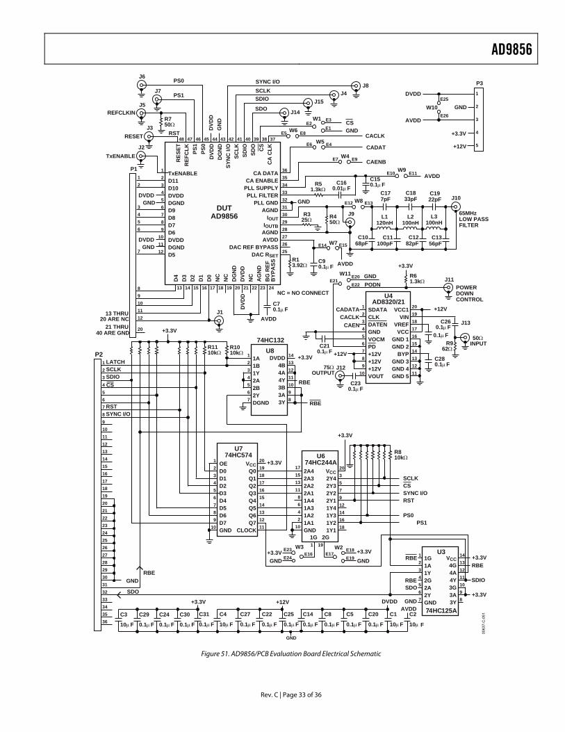
AD9856
Rev. C | Page 33 of 36
DVDD+12V+3.3V
GND
C3
10µF
C29
0.1µF
C24
0.1µF
C30
0.1µF
C31
0.1µF
C4
10µF
C27
0.1µF
C22
0.1µF
C25
0.1µF
C14
0.1µF
C8
0.1µF
C5
0.1µF
C20
0.1µF
C1
10µF
C2
10µ F
AVDD
GND
W2
VCC2Y42Y32Y22Y11Y41Y31Y21Y1
2A42A32A22A11A41A31A21A1GND
U674HC244A
1G 2G
171513118642
10
20357912141618
+3.3V
+3.3VGND
W3+3.3V
74HC132
1A1B1Y2A2B2YDGND
DVDD4B4A4Y3B3A3Y
U8
123456789101112131415161718192021222324252627282930313233343536
CS
RBE +3.3VRBE
SDIO
+3.3VSDO
GND
P2
74HC125A
1G1A1Y2G2A2YGND
VCC4G4A4Y3G3A3Y
U3 141312111098
1234567
RBE
VCCQ0Q1Q2Q3Q4Q5Q6Q7
CLOCK
OED0D1D2D3D4D5D6D7GND
U774HC574
+3.3V
R810kΩ
+3.3V
R1110kΩ
R1010kΩ
SCLKCSSYNC I/ORST
PS0PS1
GND
RBE
+3.3V
RBE
LATCHSCLKSDIO
RSTSYNC I/O
E23
E24E16
191
E17E18
E19
+3.3V
CADATA 20191817161514131211
123456789
10
VCC1VIN
VREFVCC
GND 1GND 2
BYPGND 3GND 4GND 5
SDATACLKDATENGNDVOCMPD+12V+12V+12VVOUT
U4AD8320/21
C280.1µF
+12VCACLK
CAEN
R962Ω
J13
+12V
J12
C230.1µF
75ΩOUTPUT
J11GNDW11
PODNR61.3kΩ
C260.1µF
C210.1µF
E20E21
E22
RBE
SDO
123456789
10
20191817161514131211
POWERDOWNCONTROL
50ΩINPUT
0.1µF
141312111098
1234567
0063
7-C
-051
48 47 45 42 40 38
J3RST
SYNC I/O J8SCLK J4
SDO J14
CACLK
J6
J7
J5
R750Ω
PS0
PS1
CAENB
R13.92Ω
GNDDVDD C17
7pFC1833pF
C1922pF
L1120nH
L2100nH
L3100nH
C1068pF
C11100pF
C1282pF
C1356pF
J9
C160.01µF
R51.3kΩ
C150.1µF
13 THRU20 ARE NC
21 THRU40 ARE GND
J2
TxENABLED11D10DVDDDGNDD9D8D7D6DVDDDGNDD5
CA DATACA ENABLE
PLL SUPPLYPLL FILTER
PLL GNDAGND
IOUTIOUTB
AGNDAVDD
DAC REF BYPASSDAC RSET
363534333231302928272625
J10
RES
ETR
EFC
LK PS1
PS0
DVD
DD
GN
DSY
NC
I/OSC
LKSD
IOSD
O CS
CA
CLK
D4
D3
D2
D1
D0
NC
NC
DG
ND
DVD
DN
CA
GN
DB
G R
EFB
YPA
SS
13 15 16 17 18
123456789
101112
12
3456
7
89101112
20
GNDDVDD
P1
GN
DD
VDD
DUTAD9856
SDIO J15
GND
W6
W5
W4CADAT
AVDD
C90.1µF
W7
AVDD
R325Ω R4
50Ω
DVD
D
C70.1µF
AVDDJ1
W8
CSGND
W1
E14 E15
E12 E13
W9E10 E11
E7 E9
E6 E4
E5 E8
E2E3
E1
P3
GND
+3.3V
+12V
1
2
3
4
5
AVDD
DVDD
W10E25
E26REFCLKIN
TxENABLE
65MHzLOW PASSFILTER
RESET
NC = NO CONNECT
46 44 43 41 39 37
14 19 20 21 22 23 24
Figure 51. AD9856/PCB Evaluation Board Electrical Schematic
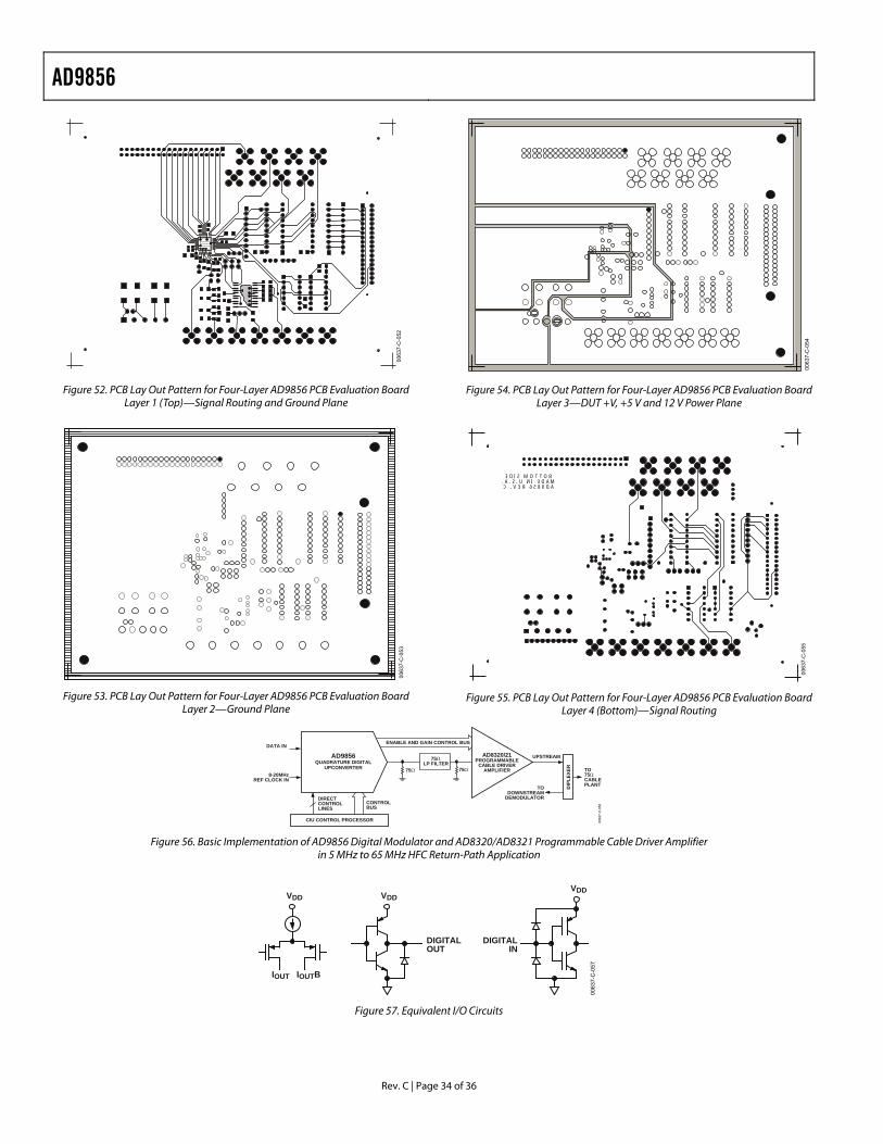
AD9856
Rev. C | Page 34 of 36
0063
7-C
-052
Figure 52. PCB Lay Out Pattern for Four-Layer AD9856 PCB Evaluation Board Layer 1 (Top)—Signal Routing and Ground Plane
0063
7-C
-053
Figure 53. PCB Lay Out Pattern for Four-Layer AD9856 PCB Evaluation Board Layer 2—Ground Plane
0063
7-C
-054
Figure 54. PCB Lay Out Pattern for Four-Layer AD9856 PCB Evaluation Board Layer 3—DUT +V, +5 V and 12 V Power Plane
BOTTOMSIDEMADEINU.S.A.AD9856REV.C
0063
7-C
-055
Figure 55. PCB Lay Out Pattern for Four-Layer AD9856 PCB Evaluation Board Layer 4 (Bottom)—Signal Routing
AD8320/21PROGRAMMABLE
CABLE DRIVERAMPLIFIER
ENABLE AND GAIN CONTROL BUS
75ΩLP FILTER
AD9856QUADRATURE DIGITAL
UPCONVERTER
CIU CONTROL PROCESSOR
DIRECTCONTROLLINES
CONTROLBUS
75Ω
DIP
LEXE
R TO75ΩCABLEPLANT
UPSTREAM
TODOWNSTREAM
DEMODULATOR
75Ω
DATA IN
8-20MHzREF CLOCK IN
0063
7-C
-056
Figure 56. Basic Implementation of AD9856 Digital Modulator and AD8320/AD8321 Programmable Cable Driver Amplifier in 5 MHz to 65 MHz HFC Return-Path Application
VDD
DIGITALOUT
IOUT IOUTB
VDDVDD
DIGITALIN
0063
7-C
-057
Figure 57. Equivalent I/O Circuits
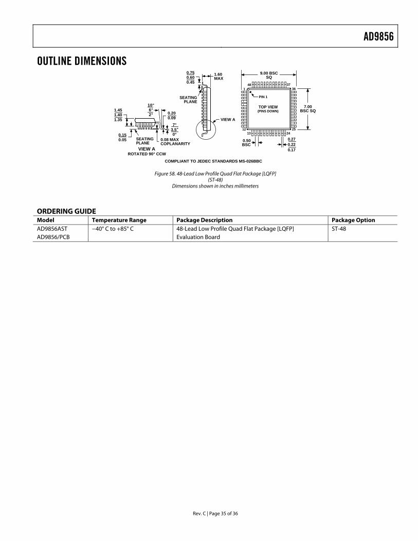
AD9856
Rev. C | Page 35 of 36
OUTLINE DIMENSIONS
TOP VIEW(PINS DOWN)
1
1213
2524
363748
0.270.220.17
0.50BSC
7.00BSC SQ
SEATINGPLANE
1.60MAX
0.750.600.45
VIEW A
9.00 BSCSQ
PIN 1
0.200.09
1.451.401.35
0.08 MAXCOPLANARITY
VIEW AROTATED 90° CCW
SEATINGPLANE
10°6°2°
7°3.5°0°0.15
0.05
COMPLIANT TO JEDEC STANDARDS MS-026BBC
Figure 58. 48-Lead Low Profile Quad Flat Package [LQFP] (ST-48)
Dimensions shown in inches millimeters
ORDERING GUIDE Model Temperature Range Package Description Package Option AD9856AST −40° C to +85° C 48-Lead Low Profile Quad Flat Package [LQFP] ST-48 AD9856/PCB Evaluation Board

AD9856
Rev. C | Page 36 of 36
NOTES
© 2005 Analog Devices, Inc. All rights reserved. Trademarks and registered trademarks are the property of their respective owners. C00637–0–1/05(C)