ald atomic layer deposition - swissphotonics · pdf fileald atomic layer deposition. 1. ......
TRANSCRIPT

Laboratoire des Technologies de la Microélectronique (LTM)
Univ. Grenoble Alpes, Lab. LTM (CEA-LETI/MINATEC) - Grenoble – France
Christophe Vallée
ALD
Atomic Layer Deposition

1. Atomic Layer Deposition
2. ALD set-up: thermal, plasma assisted, batch, temporal vs spatial
3. ALD for SC / Barrier layer / optics
4. Conclusions

Atomic Layer Deposition
Atomic Layer Deposition (ALD) is a sort of CVD process where precursors are admitted
separately and alternately into the reactor
Advantages:
Self-limiting surface reactions relatively
insensitive to gas pressure and temperature:
→ Conformal in nm-scale features to aspect
ratios of e.g. 100:1
→ Pinhole-free films
→ Uniform across m-scale objects
→ Low impurity levels, high quality
→ Å-level control of thickness
→ i.e. slow
Disadvantages:
Very low growth rate (1Å/cycle)
time for cycle ~ few seconds to tens of seconds
Ref: "Technology Backgrounder: Atomic Layer Deposition," IC Knowledge LLC, 24 April 06. <www.icknowledge.com/misc_technology/Atomic%20Layer%20Deposition%20Briefing.pdf>.

Atomic Layer Deposition
Reactant gas
OFF
ON
Precursor
OFF
ON
Reactant gas
OFF
ON
Pulsing the
precursor ON
OFF
Pulsed CVD with DLI
Precursor
Purge
Reactant gas
1
2 4
3OFF
ON
OFF
ON
OFF
ON
CVD
ALD
time time time
1 ALD cycle = 4 steps : precursor / purge / reactant / purge
E Langereis et al, 2009 J. Phys.
D: Appl. Phys. 42 073001
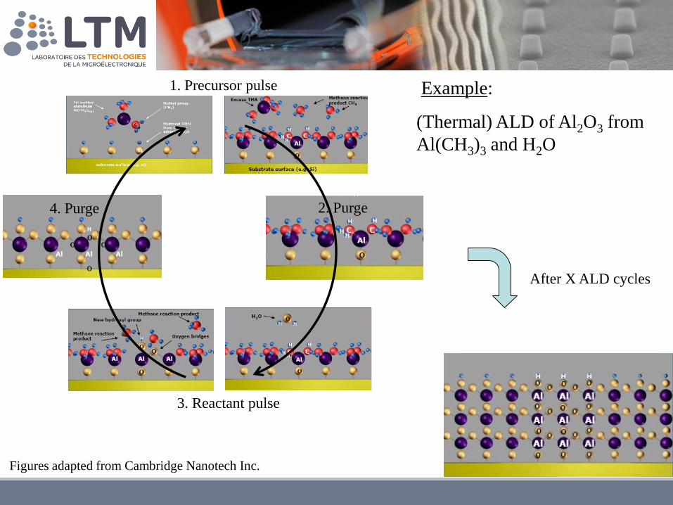
Example:
(Thermal) ALD of Al2O3 from
Al(CH3)3 and H2O
1. Precursor pulse
3. Reactant pulse
4. Purge 2. Purge
After X ALD cycles
Figures adapted from Cambridge Nanotech Inc.

ALD of hafnium oxide from HfCl4 and water
Video from
S. Elliott (Tyndall)
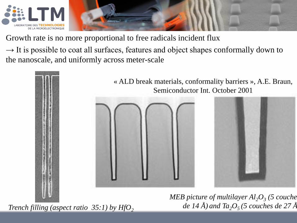
MEB picture of multilayer Al2O3 (5 couches
de 14 Å) and Ta2O5 (5 couches de 27 Å)
« ALD break materials, conformality barriers », A.E. Braun,
Semiconductor Int. October 2001
Growth rate is no more proportional to free radicals incident flux
→ It is possible to coat all surfaces, features and object shapes conformally down to
the nanoscale, and uniformly across meter-scale
Trench filling (aspect ratio 35:1) by HfO2
1. Atomic Layer Deposition
2. ALD set-up: thermal, plasma assisted, batch, temporal vs
spatial
3. ALD for SC / barrier layer / optics
4. Conclusions

Cross flow / Traveling Wave Reactor
Typical pressure 1-10 Torr
Sources: Univ. Colorado
Batch ALD
Large reactor volume
Typically long deposition runs with
50-100 planes substrates in parallel

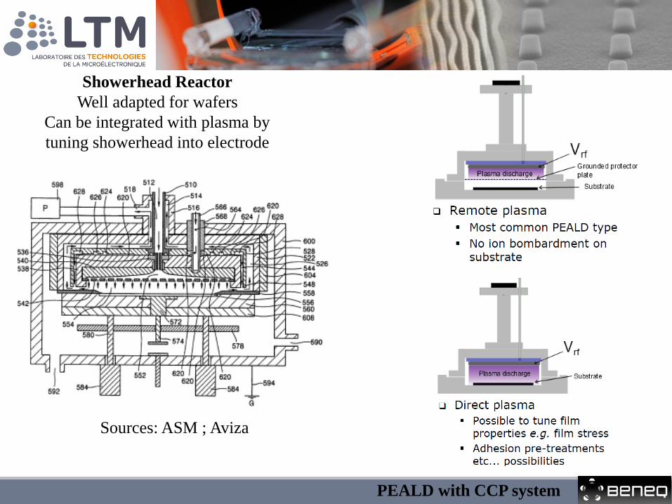
Showerhead Reactor
Well adapted for wafers
Can be integrated with plasma by
tuning showerhead into electrode
Sources: ASM ; Aviza
PEALD with CCP system

PEALD with remote plasma
Source: TU Eindhoven

1)
2)
3) Purge 4) 5) Purge
Al(CH3)3 exposure
Surface Initiale
H2O exposureO2 plasma
exposure
O2 plasma
Al2O3 - Al(CH3)3 and O2 plasma
Comparison between
thermal ALD and PE-ALD
From Oxford instrumentProfijt et al., J. Vac. Sci. Technol. A 29 (5) 050801 (2011)
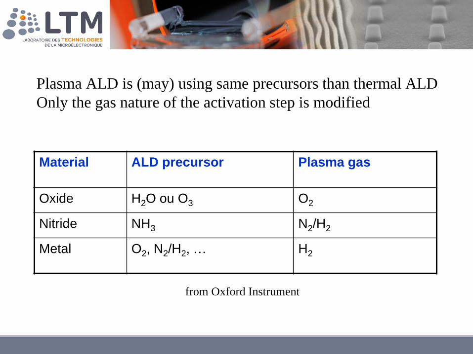
Plasma ALD is (may) using same precursors than thermal ALD
Only the gas nature of the activation step is modified
Material ALD precursor Plasma gas
Oxide H2O ou O3 O2
Nitride NH3 N2/H2
Metal O2, N2/H2, … H2
from Oxford Instrument

TEMPORAL ALD:
Precursor pulses alternate in time, separated by purges.
Substrate is stationary and is exposed to each precursor for a limited period
of time.
SPATIAL ALD:
Continuous flow of precursors limited to certain zones in space, separated
by inert gas curtains.
Substrate moves so as to alternate periodically between precursor zones.
TMA
20 ms
H2O
60 ms
Purge/Pump
2 s
Purge/Pump
4 s
> 100
cycles( )
timeTemporal ALD: deposition rate < 2 nm/min @ 100 mtorr
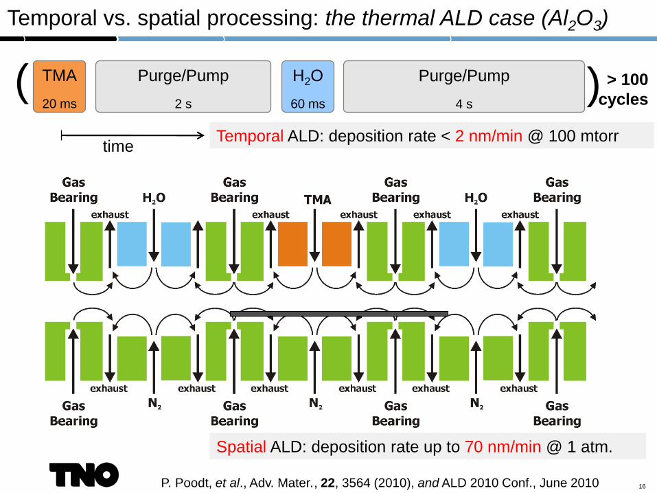
Temporal vs. spatial processing: the thermal ALD case (Al2O3)
16
Spatial ALD: deposition rate up to 70 nm/min @ 1 atm.
P. Poodt, et al., Adv. Mater., 22, 3564 (2010), and ALD 2010 Conf., June 2010
TMA
20 ms
H2O
60 ms
Purge/Pump
2 s
Purge/Pump
4 s
> 100
cycles( )
timeTemporal ALD: deposition rate < 2 nm/min @ 100 mtorr

From Lotus Technology, Beneq
Spatial ALD with
Roll to Roll system
1. Atomic Layer Deposition
2. ALD set-up: thermal, plasma assisted, batch, temporal vs spatial
3. ALD for SC / barrier layer / optics
4. Conclusions

HfO2 for CMOS: mass production by Intel since 2007 (45 nm node)
22 nm 1st generation
Tri-gate Transistor14 nm 2nd generation
Tri-gate Transistor
Source: Intel
Johnson et al., Mater. Today 17 (5), 236-246 (2014)
b: W-gate structure c: pi-gate strustured: Carbon nanotube
with gate all around
Intel Xeon PMOS transistor features embedded SiGe
(25-30% Ge) and a replacement high-k/metal gate
Semiconductor International, 5/6/2008
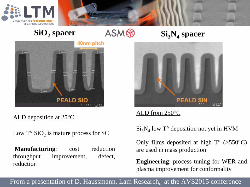
SiO2 spacer Si3N4 spacer
ALD deposition at 25°C
Low T° SiO2 is mature process for SC
Manufacturing: cost reduction
throughput improvement, defect,
reduction
ALD from 250°C
Si3N4 low T° deposition not yet in HVM
Only films deposited at high T° (>550°C)
are used in mass production
Engineering: process tuning for WER and
plasma improvement for conformality
From a presentation of D. Haussmann, Lam Research, at the AVS2015 conference

ALD allows multilayers structures
whole MIM stack could be made by ALD
Years 2009 – 2016 2017 – 2024
Top electr. TiN Ru, RuO2, Ir, IrO2
High-k ZrO2, HfO2, Ta2O5 TiO2, ATO, STO, BST
Bottom electr. TiN Ru, RuO2, Ir, IrO2, SrRuO2
Source: ITRS Roadmap
Ru on SiO2 (AR 17)
Kim et al., JES 154 (2),
D95:D101 (2007)
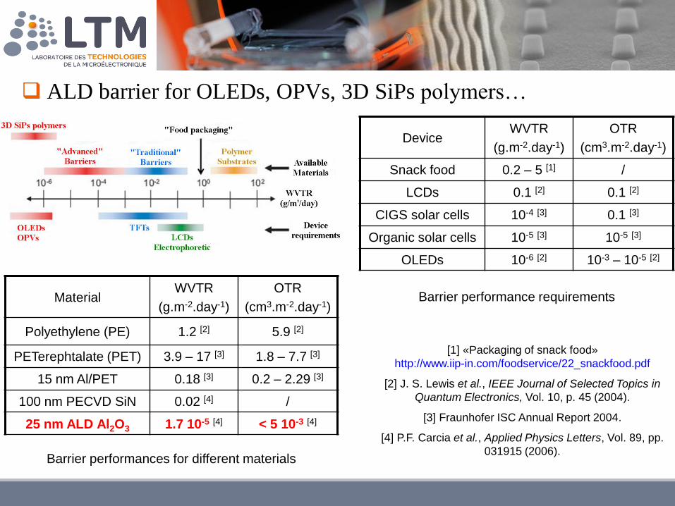
MaterialWVTR
(g.m-2.day-1)
OTR
(cm3.m-2.day-1)
Polyethylene (PE) 1.2 [2] 5.9 [2]
PETerephtalate (PET) 3.9 – 17 [3] 1.8 – 7.7 [3]
15 nm Al/PET 0.18 [3] 0.2 – 2.29 [3]
100 nm PECVD SiN 0.02 [4] /
25 nm ALD Al2O3 1.7 10-5 [4] < 5 10-3 [4]
Barrier performances for different materials
[1] «Packaging of snack food»
http://www.iip-in.com/foodservice/22_snackfood.pdf
[2] J. S. Lewis et al., IEEE Journal of Selected Topics in
Quantum Electronics, Vol. 10, p. 45 (2004).
[3] Fraunhofer ISC Annual Report 2004.
[4] P.F. Carcia et al., Applied Physics Letters, Vol. 89, pp.
031915 (2006).
DeviceWVTR
(g.m-2.day-1)
OTR
(cm3.m-2.day-1)
Snack food 0.2 – 5 [1] /
LCDs 0.1 [2] 0.1 [2]
CIGS solar cells 10-4 [3] 0.1 [3]
Organic solar cells 10-5 [3] 10-5 [3]
OLEDs 10-6 [2] 10-3 – 10-5 [2]
Barrier performance requirements
ALD barrier for OLEDs, OPVs, 3D SiPs polymers…
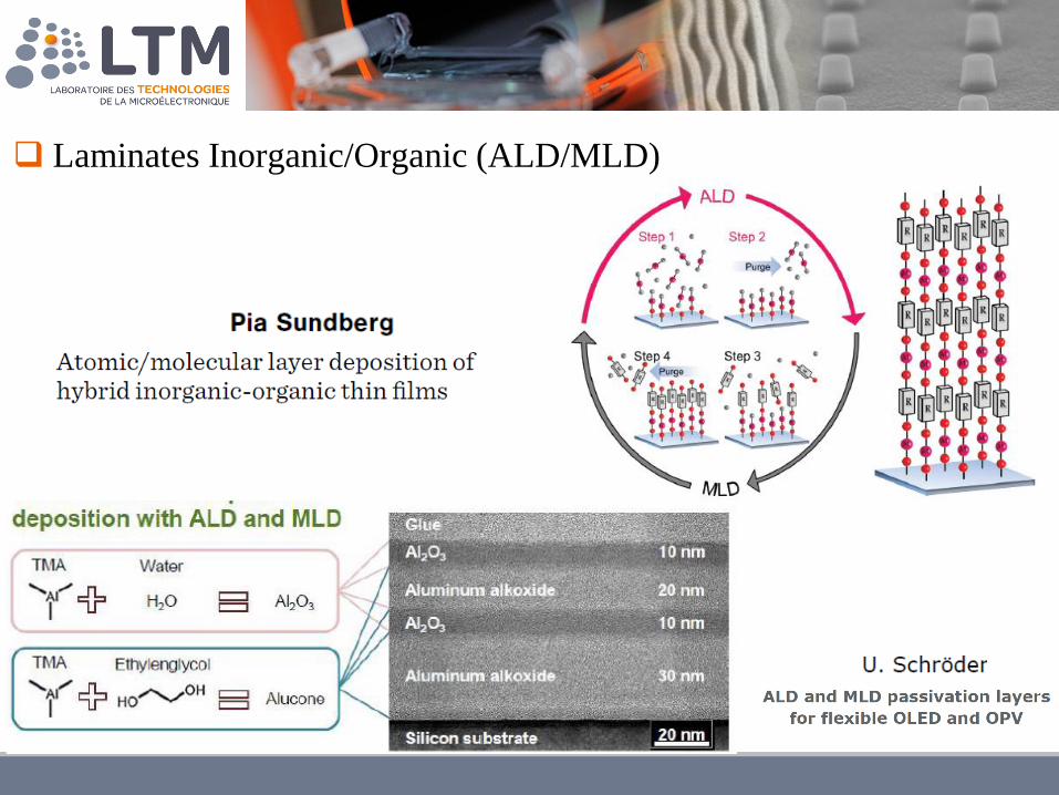
Laminates Inorganic/Organic (ALD/MLD)

ALD process delivers pinhole-free, very large optics
MLD Technologies has scaled up its
atomic-layer-deposition (ALD) process to
provide uniform (less than ±1% variation),
low-loss (typically less than 50 ppm total
loss) precision optical coatings on
substrates up to 800 mm in diameter.
Coatings are pinhole-free and can be
deposited from a number of metal-oxide
film materials.
The production-scale ALD chamber
designed and built by MLD is capable of
coating planar, 3D, and large curved
optical elements..
http://www.laserfocusworld.com/articles/print/volume-49/issue-07/newsbreaks/ald-process-delivers-pinhole-free-very-large-optics.html
http://mldtech.com/technology/atomic-layer-deposition/
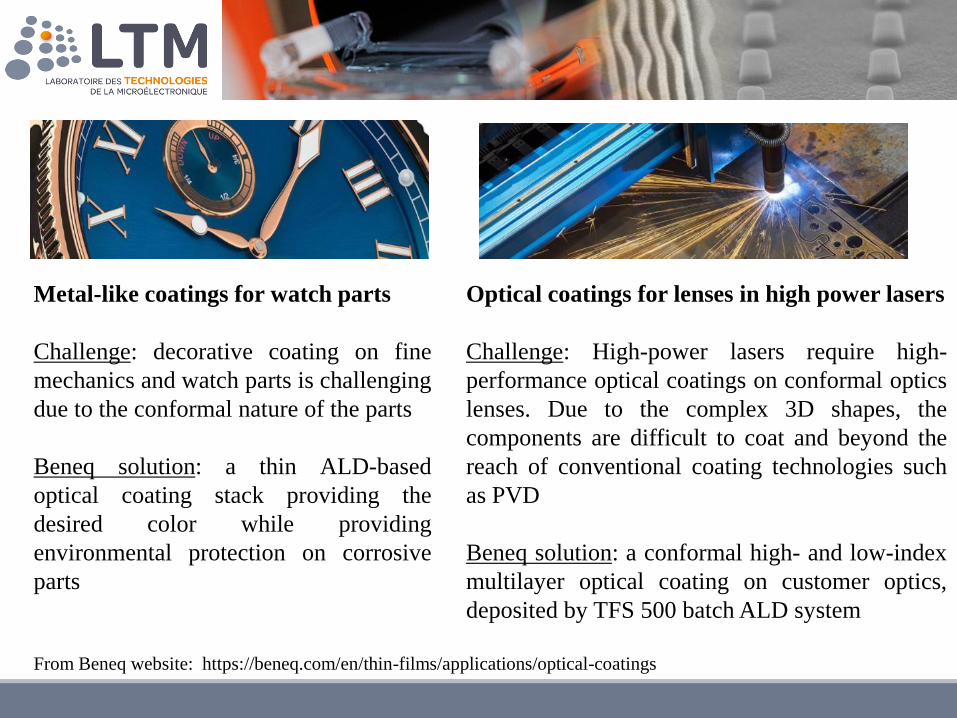
Metal-like coatings for watch parts
Challenge: decorative coating on fine
mechanics and watch parts is challenging
due to the conformal nature of the parts
Beneq solution: a thin ALD-based
optical coating stack providing the
desired color while providing
environmental protection on corrosive
parts
Optical coatings for lenses in high power lasers
Challenge: High-power lasers require high-
performance optical coatings on conformal optics
lenses. Due to the complex 3D shapes, the
components are difficult to coat and beyond the
reach of conventional coating technologies such
as PVD
Beneq solution: a conformal high- and low-index
multilayer optical coating on customer optics,
deposited by TFS 500 batch ALD system
From Beneq website: https://beneq.com/en/thin-films/applications/optical-coatings

Optique / photonique
(a, b) Scanning electron micrographs
of a diffractive Fresnel zone plate X-
ray lens where ALD Ir has been
deposited on a hydrogen
silsesquioxane resist template to
double the frequency of the
diffractive rings.
(c−f) High-magnification top and tilted
images
(c, e) before and (d, f) after ALD Ir
coating.
1. Atomic Layer Deposition
2. ALD set-up: thermal, plasma assisted, batch, temporal vs spatial
3. ALD for SC / passivation / optics
4. Conclusions
ALD is a unique self-limiting process for growing ultra-thin
pinhole-free films that is enabling new developments in high-tech
manufacturing sectors such as electronics, energy and coatings
ALD gives highly conformal and dense films (1 – 100 nm)
Just a few review articles:
S. M. George, Chem. Rev. 110, 111 (2010)
R. L. Puurunen, J. Appl. Phys. 97, 121301 (2005)
V. Miikkulainen, M. Leskelä, M. Ritala, R. L. Puurunen, J. Appl. Phys. 113,
021301 (2013)
H.B. Profijt et al, J. Vac. Sci. Technol. A 29, 050801 (2011)

Number of delegates at annual International Conference on Atomic Layer
Deposition has grown by factor of 4 in the last decade. At the 2016 conference, 150
companies attended, comprising 50% of the delegates, of which 50 were exhibitors
and 26 were sponsors.
https://aldconference.avs.org/

European action for ALD: COST HERALDHooking together European research in Atomic Layer Deposition
French research group: GDR RAFALD + workshop RAFALDRéseau des Acteurs Français de l'ALD
7-9 Nov. Montpellier (France)
http://www.european-ald.net/
https://sites.google.com/site/rafaldepot/home

Thank you for your attention