am335x pru-icss reference guide (rev. a)
TRANSCRIPT

AM335x PRU-ICSS Reference Guide
Literature Number: SPRUHF8AMay 2012–Revised June 2013

Contents
1 Introduction ...................................................................................................................... 131.1 Features ................................................................................................................. 15
2 Integration ........................................................................................................................ 162.1 PRU-ICSS Connectivity Attributes ................................................................................... 172.2 PRU-ICSS Clock and Reset Management ......................................................................... 172.3 PRU-ICSS Pin List ..................................................................................................... 18
3 PRU-ICSS Register Overview .............................................................................................. 193.1 Local Memory Map .................................................................................................... 193.2 Global Memory Map ................................................................................................... 20
4 PRU-ICSS Internal Pinmux Overview .................................................................................... 215 PRU ................................................................................................................................. 23
5.1 Introduction ............................................................................................................. 235.2 Functional Description ................................................................................................. 255.3 Basic Programming Model ............................................................................................ 365.4 PRUSS_PRU_CTRL Registers ...................................................................................... 755.5 PRU_ICSS_PRU_DEBUG Registers ............................................................................... 85
6 Interrupt Controller .......................................................................................................... 1526.1 Introduction ............................................................................................................ 1526.2 Functional Description ............................................................................................... 1536.3 Basic Programming Model .......................................................................................... 1566.4 PRU_ICSS_INTC Registers ........................................................................................ 156
7 PRU-ICSS Interrupts ......................................................................................................... 2228 Universal Asynchronous Receiver/Transmitter .................................................................... 224
8.1 Introduction ............................................................................................................ 2248.2 Functional Description ............................................................................................... 2268.3 Registers .............................................................................................................. 237
9 Industrial Ethernet Peripheral (IEP) .................................................................................... 2569.1 Introduction ............................................................................................................ 2569.2 Functional Description ............................................................................................... 2569.3 PRU_ICSS_IEP Registers .......................................................................................... 256
10 CFG ................................................................................................................................ 27210.1 PRU_ICSS_CFG Registers ......................................................................................... 272
2 SPRUHF8A–May 2012–Revised June 2013

List of Figures1 Block Diagram ............................................................................................................. 142 PRU-ICSS Integration..................................................................................................... 163 PRU-ICSS Internal Signal Muxing: pin_mux_sel[0]................................................................... 214 PRU-ICSS Internal Signal Muxing: pin_mux_sel[1]................................................................... 225 PRU Block Diagram ....................................................................................................... 246 PRU R31 (GPI) Direct Connection Mode Block Diagram ............................................................ 287 PRU R31 (GPI) 16-Bit Parallel Capture Mode Block Diagram ...................................................... 288 PRU R31 (GPI) 28-Bit Shift Mode....................................................................................... 299 PRU R30 (GPO) Direct Connection Mode Block Diagram........................................................... 3010 PRU R30 (GPO) Shift Out Mode Block Diagram...................................................................... 3011 Integration of the PRU and MAC ........................................................................................ 3212 Multiply-Only Mode Functional Diagram................................................................................ 3313 Multiply and Accumulate Mode Functional Diagram.................................................................. 3314 Integration of PRU and Scratch Pad.................................................................................... 3415 PRU Peripherals Mapped to PRU Transfer Bus ...................................................................... 6816 Possible Implementations of a 32-Byte Data Window Peripheral................................................... 6817 PRU Registers Mapped into Multiple Internal Device Registers .................................................... 6918 CONTROL Register ....................................................................................................... 7619 STATUS Register ......................................................................................................... 7820 WAKEUP_EN Register ................................................................................................... 7921 CYCLE Register ........................................................................................................... 8022 STALL Register ............................................................................................................ 8123 CTBIR0 Register........................................................................................................... 8224 CTBIR1 Register........................................................................................................... 8325 CTPPR0 Register ......................................................................................................... 8426 CTPPR1 Register ......................................................................................................... 8527 GPREG0 Register ......................................................................................................... 8828 GPREG1 Register ......................................................................................................... 8929 GPREG2 Register ......................................................................................................... 9030 GPREG3 Register ......................................................................................................... 9131 GPREG4 Register ......................................................................................................... 9232 GPREG5 Register ......................................................................................................... 9333 GPREG6 Register ......................................................................................................... 9434 GPREG7 Register ......................................................................................................... 9535 GPREG8 Register ......................................................................................................... 9636 GPREG9 Register ......................................................................................................... 9737 GPREG10 Register ....................................................................................................... 9838 GPREG11 Register ....................................................................................................... 9939 GPREG12 Register ...................................................................................................... 10040 GPREG13 Register ...................................................................................................... 10141 GPREG14 Register ...................................................................................................... 10242 GPREG15 Register ...................................................................................................... 10343 GPREG16 Register ...................................................................................................... 10444 GPREG17 Register ...................................................................................................... 10545 GPREG18 Register ...................................................................................................... 10646 GPREG19 Register ...................................................................................................... 10747 GPREG20 Register ...................................................................................................... 108
3SPRUHF8A–May 2012–Revised June 2013

48 GPREG21 Register ...................................................................................................... 10949 GPREG22 Register ...................................................................................................... 11050 GPREG23 Register ...................................................................................................... 11151 GPREG24 Register ...................................................................................................... 11252 GPREG25 Register ...................................................................................................... 11353 GPREG26 Register ...................................................................................................... 11454 GPREG27 Register ...................................................................................................... 11555 GPREG28 Register ...................................................................................................... 11656 GPREG29 Register ...................................................................................................... 11757 GPREG30 Register ...................................................................................................... 11858 GPREG31 Register ...................................................................................................... 11959 CT_REG0 Register ...................................................................................................... 12060 CT_REG1 Register ...................................................................................................... 12161 CT_REG2 Register ...................................................................................................... 12262 CT_REG3 Register ...................................................................................................... 12363 CT_REG4 Register ...................................................................................................... 12464 CT_REG5 Register ...................................................................................................... 12565 CT_REG6 Register ...................................................................................................... 12666 CT_REG7 Register ...................................................................................................... 12767 CT_REG8 Register ...................................................................................................... 12868 CT_REG9 Register ...................................................................................................... 12969 CT_REG10 Register..................................................................................................... 13070 CT_REG11 Register..................................................................................................... 13171 CT_REG12 Register..................................................................................................... 13272 CT_REG13 Register..................................................................................................... 13373 CT_REG14 Register..................................................................................................... 13474 CT_REG15 Register..................................................................................................... 13575 CT_REG16 Register..................................................................................................... 13676 CT_REG17 Register..................................................................................................... 13777 CT_REG18 Register..................................................................................................... 13878 CT_REG19 Register..................................................................................................... 13979 CT_REG20 Register..................................................................................................... 14080 CT_REG21 Register..................................................................................................... 14181 CT_REG22 Register..................................................................................................... 14282 CT_REG23 Register..................................................................................................... 14383 CT_REG24 Register..................................................................................................... 14484 CT_REG25 Register..................................................................................................... 14585 CT_REG26 Register..................................................................................................... 14686 CT_REG27 Register..................................................................................................... 14787 CT_REG28 Register..................................................................................................... 14888 CT_REG29 Register..................................................................................................... 14989 CT_REG30 Register..................................................................................................... 15090 CT_REG31 Register..................................................................................................... 15191 Interrupt Controller Block Diagram .................................................................................... 15392 Flow of System Interrupts to Host ..................................................................................... 15493 REVID Register .......................................................................................................... 15994 CR Register............................................................................................................... 16095 GER Register............................................................................................................. 16196 GNLR Register ........................................................................................................... 162
4 SPRUHF8A–May 2012–Revised June 2013

97 SISR Register ............................................................................................................ 16398 SICR Register ............................................................................................................ 16499 EISR Register ............................................................................................................ 165100 EICR Register ............................................................................................................ 166101 HIEISR Register.......................................................................................................... 167102 HIDISR Register ......................................................................................................... 168103 GPIR Register ............................................................................................................ 169104 SRSR0 Register.......................................................................................................... 170105 SRSR1 Register.......................................................................................................... 171106 SECR0 Register.......................................................................................................... 172107 SECR1 Register.......................................................................................................... 173108 ESR0 Register............................................................................................................ 174109 ERS1 Register............................................................................................................ 175110 ECR0 Register ........................................................................................................... 176111 ECR1 Register ........................................................................................................... 177112 CMR0 Register ........................................................................................................... 178113 CMR1 Register ........................................................................................................... 179114 CMR2 Register ........................................................................................................... 180115 CMR3 Register ........................................................................................................... 181116 CMR4 Register ........................................................................................................... 182117 CMR5 Register ........................................................................................................... 183118 CMR6 Register ........................................................................................................... 184119 CMR7 Register ........................................................................................................... 185120 CMR8 Register ........................................................................................................... 186121 CMR9 Register ........................................................................................................... 187122 CMR10 Register ......................................................................................................... 188123 CMR11 Register ......................................................................................................... 189124 CMR12 Register ......................................................................................................... 190125 CMR13 Register ......................................................................................................... 191126 CMR14 Register ......................................................................................................... 192127 CMR15 Register ......................................................................................................... 193128 HMR0 Register ........................................................................................................... 194129 HMR1 Register ........................................................................................................... 195130 HMR2 Register ........................................................................................................... 196131 HIPIR0 Register .......................................................................................................... 197132 HIPIR1 Register .......................................................................................................... 198133 HIPIR2 Register .......................................................................................................... 199134 HIPIR3 Register .......................................................................................................... 200135 HIPIR4 Register .......................................................................................................... 201136 HIPIR5 Register .......................................................................................................... 202137 HIPIR6 Register .......................................................................................................... 203138 HIPIR7 Register .......................................................................................................... 204139 HIPIR8 Register .......................................................................................................... 205140 HIPIR9 Register .......................................................................................................... 206141 SIPR0 Register ........................................................................................................... 207142 SIPR1 Register ........................................................................................................... 208143 SITR0 Register ........................................................................................................... 209144 SITR1 Register ........................................................................................................... 210145 HINLR0 Register ......................................................................................................... 211
5SPRUHF8A–May 2012–Revised June 2013

146 HINLR1 Register ......................................................................................................... 212147 HINLR2 Register ......................................................................................................... 213148 HINLR3 Register ......................................................................................................... 214149 HINLR4 Register ......................................................................................................... 215150 HINLR5 Register ......................................................................................................... 216151 HINLR6 Register ......................................................................................................... 217152 HINLR7 Register ......................................................................................................... 218153 HINLR8 Register ......................................................................................................... 219154 HINLR9 Register ......................................................................................................... 220155 HIER Register ............................................................................................................ 221156 UART Block Diagram.................................................................................................... 225157 UART Clock Generation Diagram ..................................................................................... 226158 Relationships Between Data Bit, BCLK, and UART Input Clock .................................................. 227159 UART Protocol Formats................................................................................................. 229160 UART Interface Using Autoflow Diagram ............................................................................. 232161 Autoflow Functional Timing Waveforms for UARTn_RTS ......................................................... 233162 Autoflow Functional Timing Waveforms for UARTn_CTS ......................................................... 233163 UART Interrupt Request Enable Paths ............................................................................... 235164 Receiver Buffer Register (RBR)........................................................................................ 238165 Transmitter Holding Register (THR) ................................................................................... 239166 Interrupt Enable Register (IER) ........................................................................................ 240167 Interrupt Identification Register (IIR)................................................................................... 241168 FIFO Control Register (FCR) ........................................................................................... 243169 Line Control Register (LCR) ............................................................................................ 244170 Modem Control Register (MCR) ....................................................................................... 246171 Line Status Register (LSR) ............................................................................................. 247172 Modem Status Register (MSR)......................................................................................... 250173 Scratch Pad Register (SCR)............................................................................................ 251174 Divisor LSB Latch (DLL) ................................................................................................ 252175 Divisor MSB Latch (DLH) ............................................................................................... 252176 Revision Identification Register 1 (REVID1).......................................................................... 253177 Revision Identification Register 2 (REVID2).......................................................................... 253178 Power and Emulation Management Register (PWREMU_MGMT)................................................ 254179 Mode Definition Register (MDR) ....................................................................................... 255180 GLOBAL_CFG Register................................................................................................. 258181 GLOBAL_STATUS Register............................................................................................ 259182 COMPEN Register....................................................................................................... 260183 COUNT Register ......................................................................................................... 261184 CMP_CFG Register ..................................................................................................... 262185 CMP_STATUS Register ................................................................................................ 263186 CMP0 Register ........................................................................................................... 264187 CMP1 Register ........................................................................................................... 265188 CMP2 Register ........................................................................................................... 266189 CMP3 Register ........................................................................................................... 267190 CMP4 Register ........................................................................................................... 268191 CMP5 Register ........................................................................................................... 269192 CMP6 Register ........................................................................................................... 270193 CMP7 Register ........................................................................................................... 271194 REVID Register .......................................................................................................... 273
6 SPRUHF8A–May 2012–Revised June 2013

195 SYSCFG Register........................................................................................................ 274196 GPCFG0 Register........................................................................................................ 275197 GPCFG1 Register........................................................................................................ 277198 CGR Register............................................................................................................. 279199 ISRP Register ............................................................................................................ 281200 ISP Register .............................................................................................................. 282201 IESP Register ............................................................................................................ 283202 IECP Register ............................................................................................................ 284203 PMAO Register........................................................................................................... 285204 MII_RT Register.......................................................................................................... 286205 IEPCLK Register ......................................................................................................... 287206 SPP Register ............................................................................................................. 288207 PIN_MX Register......................................................................................................... 289
7SPRUHF8A–May 2012–Revised June 2013

List of Tables1 PRU-ICSS Connectivity Attributes ...................................................................................... 172 PRU-ICSS Clock Signals ................................................................................................. 173 PRU-ICSS Pin List ........................................................................................................ 184 Local Instruction Memory Map........................................................................................... 195 Local Data Memory Map ................................................................................................. 196 Global Memory Map....................................................................................................... 207 PRU-ICSS Internal Signal Muxing: pin_mux_sel[0]................................................................... 218 PRU-ICSS Internal Signal Muxing: pin_mux_sel[1]................................................................... 219 PRU0/1 Constant Table .................................................................................................. 2510 Real-Time Status Interface Mapping (R31) Field Descriptions...................................................... 2611 Event Interface Mapping (R31) Field Descriptions.................................................................... 2612 PRU 31 (GPI) Modes ..................................................................................................... 2713 GPI Mode Descriptions ................................................................................................... 2714 Effective Clock Values .................................................................................................... 2815 PRU R30 (GPO) Output Mode .......................................................................................... 2916 GPO Mode Descriptions.................................................................................................. 2917 Effective Clock Values .................................................................................................... 3018 MAC_CTRL_STATUS Register (R25) Field Descriptions............................................................ 3219 Scratch Pad XFR ID ...................................................................................................... 3520 Scratch Pad XFR Collision Conditions ................................................................................. 3521 Register Byte Mapping in Little Endian ................................................................................. 5322 SBBO Result for Little Endian Mode.................................................................................... 5323 First Byte Affected in Little Endian Mode............................................................................... 5324 Register Addressing in Little Endian .................................................................................... 5425 PRUSS_PRU_CTRL REGISTERS...................................................................................... 7526 CONTROL Register Field Descriptions................................................................................. 7627 STATUS Register Field Descriptions ................................................................................... 7828 WAKEUP_EN Register Field Descriptions ............................................................................. 7929 CYCLE Register Field Descriptions ..................................................................................... 8030 STALL Register Field Descriptions...................................................................................... 8131 CTBIR0 Register Field Descriptions .................................................................................... 8232 CTBIR1 Register Field Descriptions .................................................................................... 8333 CTPPR0 Register Field Descriptions ................................................................................... 8434 CTPPR1 Register Field Descriptions ................................................................................... 8535 PRU_ICSS_PRU_DEBUG REGISTERS............................................................................... 8536 GPREG0 Register Field Descriptions................................................................................... 8837 GPREG1 Register Field Descriptions................................................................................... 8938 GPREG2 Register Field Descriptions................................................................................... 9039 GPREG3 Register Field Descriptions................................................................................... 9140 GPREG4 Register Field Descriptions................................................................................... 9241 GPREG5 Register Field Descriptions................................................................................... 9342 GPREG6 Register Field Descriptions................................................................................... 9443 GPREG7 Register Field Descriptions................................................................................... 9544 GPREG8 Register Field Descriptions................................................................................... 9645 GPREG9 Register Field Descriptions................................................................................... 9746 GPREG10 Register Field Descriptions ................................................................................. 9847 GPREG11 Register Field Descriptions ................................................................................. 99
8 SPRUHF8A–May 2012–Revised June 2013

48 GPREG12 Register Field Descriptions................................................................................ 10049 GPREG13 Register Field Descriptions................................................................................ 10150 GPREG14 Register Field Descriptions................................................................................ 10251 GPREG15 Register Field Descriptions................................................................................ 10352 GPREG16 Register Field Descriptions................................................................................ 10453 GPREG17 Register Field Descriptions................................................................................ 10554 GPREG18 Register Field Descriptions................................................................................ 10655 GPREG19 Register Field Descriptions................................................................................ 10756 GPREG20 Register Field Descriptions................................................................................ 10857 GPREG21 Register Field Descriptions................................................................................ 10958 GPREG22 Register Field Descriptions................................................................................ 11059 GPREG23 Register Field Descriptions................................................................................ 11160 GPREG24 Register Field Descriptions................................................................................ 11261 GPREG25 Register Field Descriptions................................................................................ 11362 GPREG26 Register Field Descriptions................................................................................ 11463 GPREG27 Register Field Descriptions................................................................................ 11564 GPREG28 Register Field Descriptions................................................................................ 11665 GPREG29 Register Field Descriptions................................................................................ 11766 GPREG30 Register Field Descriptions................................................................................ 11867 GPREG31 Register Field Descriptions................................................................................ 11968 CT_REG0 Register Field Descriptions ................................................................................ 12069 CT_REG1 Register Field Descriptions ................................................................................ 12170 CT_REG2 Register Field Descriptions ................................................................................ 12271 CT_REG3 Register Field Descriptions ................................................................................ 12372 CT_REG4 Register Field Descriptions ................................................................................ 12473 CT_REG5 Register Field Descriptions ................................................................................ 12574 CT_REG6 Register Field Descriptions ................................................................................ 12675 CT_REG7 Register Field Descriptions ................................................................................ 12776 CT_REG8 Register Field Descriptions ................................................................................ 12877 CT_REG9 Register Field Descriptions ................................................................................ 12978 CT_REG10 Register Field Descriptions .............................................................................. 13079 CT_REG11 Register Field Descriptions .............................................................................. 13180 CT_REG12 Register Field Descriptions .............................................................................. 13281 CT_REG13 Register Field Descriptions .............................................................................. 13382 CT_REG14 Register Field Descriptions .............................................................................. 13483 CT_REG15 Register Field Descriptions .............................................................................. 13584 CT_REG16 Register Field Descriptions .............................................................................. 13685 CT_REG17 Register Field Descriptions .............................................................................. 13786 CT_REG18 Register Field Descriptions .............................................................................. 13887 CT_REG19 Register Field Descriptions .............................................................................. 13988 CT_REG20 Register Field Descriptions .............................................................................. 14089 CT_REG21 Register Field Descriptions .............................................................................. 14190 CT_REG22 Register Field Descriptions .............................................................................. 14291 CT_REG23 Register Field Descriptions .............................................................................. 14392 CT_REG24 Register Field Descriptions .............................................................................. 14493 CT_REG25 Register Field Descriptions .............................................................................. 14594 CT_REG26 Register Field Descriptions .............................................................................. 14695 CT_REG27 Register Field Descriptions .............................................................................. 14796 CT_REG28 Register Field Descriptions .............................................................................. 148
9SPRUHF8A–May 2012–Revised June 2013

97 CT_REG29 Register Field Descriptions .............................................................................. 14998 CT_REG30 Register Field Descriptions .............................................................................. 15099 CT_REG31 Register Field Descriptions .............................................................................. 151100 PRU_ICSS_INTC REGISTERS........................................................................................ 156101 REVID Register Field Descriptions .................................................................................... 159102 CR Register Field Descriptions ........................................................................................ 160103 GER Register Field Descriptions ...................................................................................... 161104 GNLR Register Field Descriptions ..................................................................................... 162105 SISR Register Field Descriptions ...................................................................................... 163106 SICR Register Field Descriptions ...................................................................................... 164107 EISR Register Field Descriptions ...................................................................................... 165108 EICR Register Field Descriptions ...................................................................................... 166109 HIEISR Register Field Descriptions ................................................................................... 167110 HIDISR Register Field Descriptions ................................................................................... 168111 GPIR Register Field Descriptions...................................................................................... 169112 SRSR0 Register Field Descriptions ................................................................................... 170113 SRSR1 Register Field Descriptions ................................................................................... 171114 SECR0 Register Field Descriptions ................................................................................... 172115 SECR1 Register Field Descriptions ................................................................................... 173116 ESR0 Register Field Descriptions ..................................................................................... 174117 ERS1 Register Field Descriptions ..................................................................................... 175118 ECR0 Register Field Descriptions ..................................................................................... 176119 ECR1 Register Field Descriptions ..................................................................................... 177120 CMR0 Register Field Descriptions..................................................................................... 178121 CMR1 Register Field Descriptions..................................................................................... 179122 CMR2 Register Field Descriptions..................................................................................... 180123 CMR3 Register Field Descriptions..................................................................................... 181124 CMR4 Register Field Descriptions..................................................................................... 182125 CMR5 Register Field Descriptions..................................................................................... 183126 CMR6 Register Field Descriptions..................................................................................... 184127 CMR7 Register Field Descriptions..................................................................................... 185128 CMR8 Register Field Descriptions..................................................................................... 186129 CMR9 Register Field Descriptions..................................................................................... 187130 CMR10 Register Field Descriptions ................................................................................... 188131 CMR11 Register Field Descriptions ................................................................................... 189132 CMR12 Register Field Descriptions ................................................................................... 190133 CMR13 Register Field Descriptions ................................................................................... 191134 CMR14 Register Field Descriptions ................................................................................... 192135 CMR15 Register Field Descriptions ................................................................................... 193136 HMR0 Register Field Descriptions..................................................................................... 194137 HMR1 Register Field Descriptions..................................................................................... 195138 HMR2 Register Field Descriptions..................................................................................... 196139 HIPIR0 Register Field Descriptions.................................................................................... 197140 HIPIR1 Register Field Descriptions.................................................................................... 198141 HIPIR2 Register Field Descriptions.................................................................................... 199142 HIPIR3 Register Field Descriptions.................................................................................... 200143 HIPIR4 Register Field Descriptions.................................................................................... 201144 HIPIR5 Register Field Descriptions.................................................................................... 202145 HIPIR6 Register Field Descriptions.................................................................................... 203
10 SPRUHF8A–May 2012–Revised June 2013

146 HIPIR7 Register Field Descriptions.................................................................................... 204147 HIPIR8 Register Field Descriptions.................................................................................... 205148 HIPIR9 Register Field Descriptions.................................................................................... 206149 SIPR0 Register Field Descriptions .................................................................................... 207150 SIPR1 Register Field Descriptions .................................................................................... 208151 SITR0 Register Field Descriptions..................................................................................... 209152 SITR1 Register Field Descriptions..................................................................................... 210153 HINLR0 Register Field Descriptions................................................................................... 211154 HINLR1 Register Field Descriptions................................................................................... 212155 HINLR2 Register Field Descriptions................................................................................... 213156 HINLR3 Register Field Descriptions................................................................................... 214157 HINLR4 Register Field Descriptions................................................................................... 215158 HINLR5 Register Field Descriptions................................................................................... 216159 HINLR6 Register Field Descriptions................................................................................... 217160 HINLR7 Register Field Descriptions................................................................................... 218161 HINLR8 Register Field Descriptions................................................................................... 219162 HINLR9 Register Field Descriptions................................................................................... 220163 HIER Register Field Descriptions ...................................................................................... 221164 PRU-ICSS Interrupts .................................................................................................... 222165 Baud Rate Examples for 150-MHZ UART Input Clock and 16× Over-sampling Mode ......................... 227166 Baud Rate Examples for 150-MHZ UART Input Clock and 13× Over-sampling Mode ......................... 227167 UART Signal Descriptions .............................................................................................. 228168 Character Time for Word Lengths ..................................................................................... 231169 UART Interrupt Requests Descriptions ............................................................................... 235170 UART Registers .......................................................................................................... 237171 Receiver Buffer Register (RBR) Field Descriptions ................................................................. 238172 Transmitter Holding Register (THR) Field Descriptions............................................................. 239173 Interrupt Enable Register (IER) Field Descriptions .................................................................. 240174 Interrupt Identification Register (IIR) Field Descriptions ............................................................ 241175 Interrupt Identification and Interrupt Clearing Information .......................................................... 242176 FIFO Control Register (FCR) Field Descriptions .................................................................... 243177 Line Control Register (LCR) Field Descriptions...................................................................... 244178 Relationship Between ST, EPS, and PEN Bits in LCR ............................................................. 245179 Number of STOP Bits Generated...................................................................................... 245180 Modem Control Register (MCR) Field Descriptions ................................................................. 246181 Line Status Register (LSR) Field Descriptions ....................................................................... 247182 Modem Status Register (MSR) Field Descriptions .................................................................. 250183 Scratch Pad Register (MSR) Field Descriptions ..................................................................... 251184 Divisor LSB Latch (DLL) Field Descriptions .......................................................................... 252185 Divisor MSB Latch (DLH) Field Descriptions ......................................................................... 252186 Revision Identification Register 1 (REVID1) Field Descriptions ................................................... 253187 Revision Identification Register 2 (REVID2) Field Descriptions ................................................... 253188 Power and Emulation Management Register (PWREMU_MGMT) Field Descriptions ......................... 254189 Mode Definition Register (MDR) Field Descriptions................................................................. 255190 PRU_ICSS_IEP REGISTERS.......................................................................................... 256191 GLOBAL_CFG Register Field Descriptions .......................................................................... 258192 GLOBAL_STATUS Register Field Descriptions ..................................................................... 259193 COMPEN Register Field Descriptions ................................................................................ 260194 COUNT Register Field Descriptions................................................................................... 261
11SPRUHF8A–May 2012–Revised June 2013

195 CMP_CFG Register Field Descriptions ............................................................................... 262196 CMP_STATUS Register Field Descriptions .......................................................................... 263197 CMP0 Register Field Descriptions ..................................................................................... 264198 CMP1 Register Field Descriptions ..................................................................................... 265199 CMP2 Register Field Descriptions ..................................................................................... 266200 CMP3 Register Field Descriptions ..................................................................................... 267201 CMP4 Register Field Descriptions ..................................................................................... 268202 CMP5 Register Field Descriptions ..................................................................................... 269203 CMP6 Register Field Descriptions ..................................................................................... 270204 CMP7 Register Field Descriptions ..................................................................................... 271205 PRU_ICSS_CFG REGISTERS ........................................................................................ 272206 REVID Register Field Descriptions .................................................................................... 273207 SYSCFG Register Field Descriptions ................................................................................. 274208 GPCFG0 Register Field Descriptions ................................................................................. 275209 GPCFG1 Register Field Descriptions ................................................................................. 277210 CGR Register Field Descriptions ...................................................................................... 279211 ISRP Register Field Descriptions ...................................................................................... 281212 ISP Register Field Descriptions ........................................................................................ 282213 IESP Register Field Descriptions ...................................................................................... 283214 IECP Register Field Descriptions ...................................................................................... 284215 PMAO Register Field Descriptions .................................................................................... 285216 MII_RT Register Field Descriptions ................................................................................... 286217 IEPCLK Register Field Descriptions................................................................................... 287218 SPP Register Field Descriptions ....................................................................................... 288219 PIN_MX Register Field Descriptions .................................................................................. 289
12 SPRUHF8A–May 2012–Revised June 2013

The hardware module(s) and the features described in this Reference Guide are not supported byTexas Instruments. "Community" support may be offered at BeagleBoard.org/discuss. Theinformation contained in this Reference Guide is for informational purpose only and any use of theinformation contained herein is done so at the user's own risk. The Reference Guide, including thehardware module(s) and associated features, are provided "AS IS" and Texas Instrumentsdisclaims all warranties, express or implied, including but not limited to any implied warranties ofmerchantability or fitness for a particular purpose.
1 IntroductionThe Programmable Real-Time Unit and Industrial Communication Subsystem (PRU-ICSS) consists of dual32-bit RISC cores (Programmable Real-Time Units, or PRUs), shared, data, and instruction memories,internal peripheral modules, and an interrupt controller (INTC). The programmable nature of the PRUs,along with their access to pins and events, provide flexibility in implementing custom peripheral interfaces,fast real-time responses, power saving techniques, specialized data handling and DMA operations, and inoffloading tasks from the other processor cores of the system-on-chip (SoC).
Figure 1 shows the PRU-ICSS details. The subsystem available on this device is the next-generation PRU(PRUSSv2). Compared to the previous generation available on AM1x and OMAP-L13x, this versionincludes the following enhancements:• Additional data memory (8 KB compared with 512 B) and instruction memory (8 KB compared with 4
KB)• 12 KB Shared RAM• Enhanced GPIO (EGPIO), adding serial, parallel, and MII capture of the PRU input/output pins• Scratch pad (SPAD) shared by the PRU cores• Multiplier with optional accumulation (MAC)• Internal peripheral modules (UART, eCAP, MII_RT, MDIO, and IEP)
Similar to the previous generation, the PRUs have access to all resources on the SoC through theInterface/OCP master port, and the external host processors can access the PRU-ICSS resources throughthe Interface/OCP Master port. The Switched Central Resource (SCR) connects the various internal andexternal masters to the resources inside the PRU-ICSS. The INTC handles system input events and postsevents back to the device-level host CPU.
The PRU cores are programmed with a small, deterministic instruction set. Each PRU can operateindependently or in coordination with each other and can also work in coordination with the device-levelhost CPU. This interaction between processors is determined by the nature of the firmware loaded into thePRU’s instruction memory.
13SPRUHF8A–May 2012–Revised June 2013

PRU1 Core(8KB Program)
PRU-ICSS
PRU0 Core(8KB Program)
Data Mem0(8KB)
Data Mem1(8KB)
Shared RAM(12KB)
eCAP0
MII0_RT
IEP
UART0
CFG
32-B
it Inte
rconnect B
us
SPAD
EGP MAC
EGP MAC
INTC
Introduction
Figure 1. Block Diagram
The subsystem available on this device is the next-generation PRU (PRUSSv2).
14 SPRUHF8A–May 2012–Revised June 2013

Introduction
1.1 Features
The PRU subsystem includes the following main features:• Two PRUs each with:
– 8KB program memory– 8KB data memory– High Performance Interface/OCP Master port for accessing external memories– Enhanced GPIO (EGPIO) with async capture and serial support– Multiplier with optional accumulation (MAC)
• One scratch pad (SPAD) memory and broadside direct connect– 3 Banks of 30 32-bit registers
• 12 KB general purpose shared memory• One Interrupt Controller (INTC)
– Up to 64 input events supported– Interrupt mapping to 10 interrupt channels– 10 Host interrupts (2 to PRU0 and PRU1, 8 output to chip level)– Each system event can be enabled and disabled– Each host event can be enabled and disabled– Hardware prioritization of events
• 16 software Events generation by 2 PRUs• One Ethernet MII_RT module with two MII ports and configurable connections to PRUs*• One MDIO Port*• One Industrial Ethernet Peripheral (IEP) to manage/generate Industrial Ethernet functions
– One Industrial Ethernet timer with 10 capture* and eight compare events– Two Industrial Ethernet sync signals*– Two Industrial Ethernet 16-bit watchdog timers*– Industrial Ethernet digital IOs*
• One 16550-compatible UART with a dedicated 192-MHz clock• One Enhanced Capture Module (ECAP)• Flexible power management support• Integrated switched central resource (SCR) bus for connecting the various internal and external
masters to the resources inside the PRU-ICSS• Interface/OCP Slave port for external masters to access PRU-ICSS memories• Optional address translation for PRU transaction to External Host• All memories within the PRU-ICSS support parity
NOTE: * — Module or feature is used by EtherCAT. For availability of EtherCAT and thesefeatures, see the device features in Chapter 1, Introduction, in the AM335x ARM® Cortex™-A8 Microprocessors (MPUs) Technical Reference Manual (literature number SPRUH73).
15SPRUHF8A–May 2012–Revised June 2013

PRU-ICSS
Interface/OCP Slave port
Async
Bridge
L4 Fast
Async
Bridge
L3 Fast
OCP_HP0(Interface/OCP
Master port)
PRU0 Core(8KB Program RAM)
32-b
it Inte
rconnect S
CR
MII_RT
Data RAM0(8KB)
Data RAM1(8KB)
Shared RAM(12KB)
CFG
IndustrialEthernet
Peripheral(IEP)
UART0
eCAP pr1_ecap0_ecap_capin_apwm_o
pr1_uart0_cts_npr1_uart0_rts_npr1_uart0_rxdpr1_uart0_txd
pr1_edio_sofpr1_edio_latch_inpr1_edio_data_in/out[7:0]pr1_edc_latch0_inpr1_edc_latch1_inpr1_edc_sync0_rxdpr1_edc_sync1_txd
pr1_mii_mt0_clkpr1_mii0_rxlinkpr1_mii0_crspr1_mii0_colpr1_mii0_rxerpr1_mii0_txenpr1_mii0_txd3pr1_mii0_txd2pr1_mii0_txd1pr1_mii0_txd0pr1_mii_mr0_clkpr1_mii0_rxdvpr1_mii0_rxd3pr1_mii0_rxd2pr1_mii0_rxd1pr1_mii0_rxd0pr1_mdio_datapr1_mdio_mdclkpr1_mii_mt1_clkpr1_mii1_rxlinkpr1_mii1_crspr1_mii1_colpr1_mii1_rxerpr1_mii1_txenpr1_mii1_txd3pr1_mii1_txd2pr1_mii1_txd1pr1_mii1_txd0pr1_mii_mr1_clkpr1_mii1_rxdvpr1_mii1_rxd3pr1_mii1_rxd2pr1_mii1_rxd1pr1_mii1_rxd0
EnhancedGPIO
pr1_pru0_pru_r31[16:0]pr1_pru0_pru_r30[15:0]
Clocks/ResetPRCM
ocp_clkuart_clkiep_clk
rst_main_arst_n
Async
Bridge
L3 FastOCP_HP1
(Interface/OCPMaster port)
PRU1 Core(8KB Program RAM)
EnhancedGPIO
pr1_pru1_pru_r31[16:0]pr1_pru1_pru_r30[15:0]
To Host ARM InterruptsTo EDMA Events
To TSC_ADC EventINTC
Events from SelectPeripherals
MAC
ScratchPad
MAC
Integration
2 IntegrationThe device includes a programmable real-time unit subsystem (PRU-ICSS) consisting of two independentProgrammable Real-time Units (PRUs). Each PRU is a 32-bit Load/Store RISC processor with dedicatedmemories. The PRU-ICSS integration is shown in Figure 2.
Figure 2. PRU-ICSS Integration
For the availability of all features, see the device features in Chapter 1, Introduction, in the AM335x ARM® Cortex™-A8 Microprocessors (MPUs) Technical Reference Manual (literature number SPRUH73).
16 SPRUHF8A–May 2012–Revised June 2013
Integration
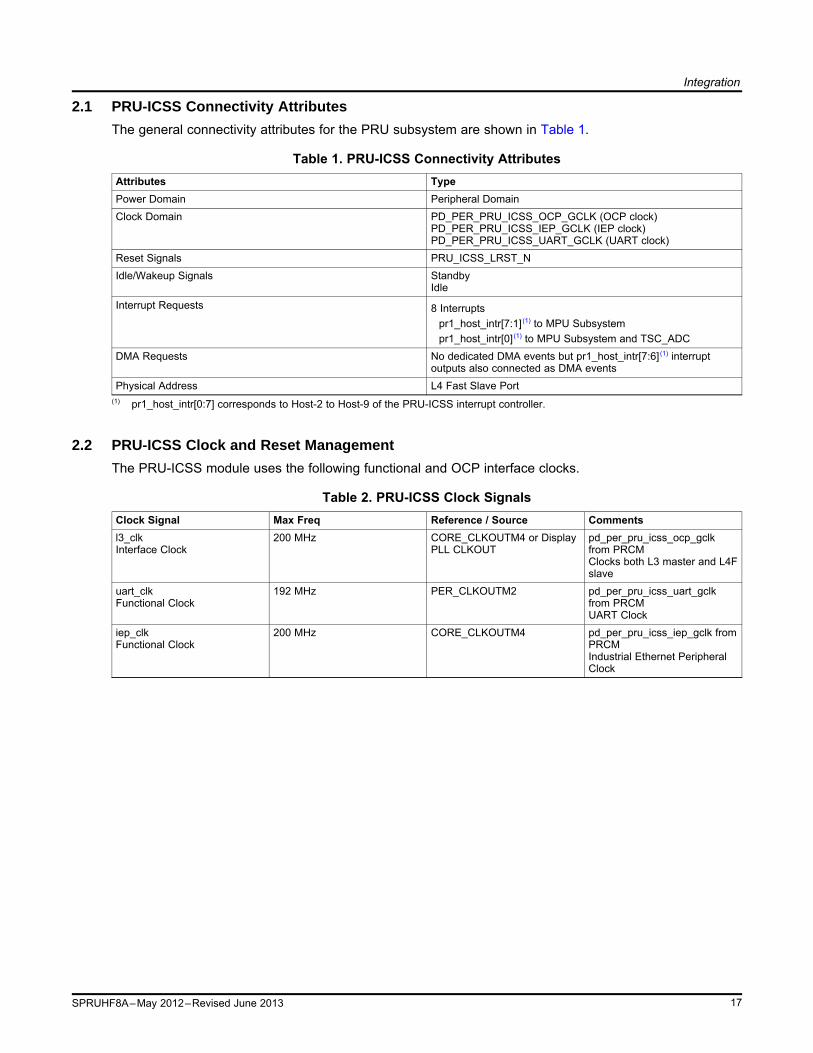
2.1 PRU-ICSS Connectivity Attributes
The general connectivity attributes for the PRU subsystem are shown in Table 1.
Table 1. PRU-ICSS Connectivity AttributesAttributes TypePower Domain Peripheral DomainClock Domain PD_PER_PRU_ICSS_OCP_GCLK (OCP clock)
PD_PER_PRU_ICSS_IEP_GCLK (IEP clock)PD_PER_PRU_ICSS_UART_GCLK (UART clock)
Reset Signals PRU_ICSS_LRST_NIdle/Wakeup Signals Standby
IdleInterrupt Requests 8 Interrupts
pr1_host_intr[7:1] (1) to MPU Subsystempr1_host_intr[0] (1) to MPU Subsystem and TSC_ADC
DMA Requests No dedicated DMA events but pr1_host_intr[7:6] (1) interruptoutputs also connected as DMA events
Physical Address L4 Fast Slave Port(1) pr1_host_intr[0:7] corresponds to Host-2 to Host-9 of the PRU-ICSS interrupt controller.
2.2 PRU-ICSS Clock and Reset Management
The PRU-ICSS module uses the following functional and OCP interface clocks.
Table 2. PRU-ICSS Clock SignalsClock Signal Max Freq Reference / Source Commentsl3_clk 200 MHz CORE_CLKOUTM4 or Display pd_per_pru_icss_ocp_gclkInterface Clock PLL CLKOUT from PRCM
Clocks both L3 master and L4Fslave
uart_clk 192 MHz PER_CLKOUTM2 pd_per_pru_icss_uart_gclkFunctional Clock from PRCM
UART Clockiep_clk 200 MHz CORE_CLKOUTM4 pd_per_pru_icss_iep_gclk fromFunctional Clock PRCM
Industrial Ethernet PeripheralClock
17SPRUHF8A–May 2012–Revised June 2013

Integration
2.3 PRU-ICSS Pin List
The PRU-ICSS external interface signals are shown in Table 3. The PRU-ICSS has a large number ofavailable I/O signals. Most of these are multiplexed with other functional signals at the chip level. Pleaserefer to the device's System Reference Guide or datasheet for specific signal availability through pinmuxing.
Table 3. PRU-ICSS Pin ListPin Type Descriptionpr1_mii_mr0_clk I MII0 Receive Clockpr1_mii0_rxdv I MII0 Receive Data Validpr1_mii0_rxd[3:0] I MII0 Receive Datapr1_mii0_rxlink I MII0 Receive Linkpr1_mii0_rxer I MII0 Receive Data Errorpr1_mii0_crs I MII0 Carrier Sensepr1_mii0_col I MII0 Carrier Sensepr1_mii_mt0_clk I MII0 Transmit Clockpr1_mii0_txen O MII0 Transmit Enablepr1_mii0_txd[3:0] O MII0 Transmit Datapr1_mii_mr1_clk I MII1 Receive Clockpr1_mii1_rxdv I MII1 Receive Data Validpr1_mii1_rxd[3:0] I MII1 Receive Datapr1_mii1_rxlink I MII1 Receive Linkpr1_mii1_rxer I MII1 Receive Data Errorpr1_mii1_crs I MII1 Carrier Sensepr1_mii1_col I MII1 Carrier Sensepr1_mii_mt1_clk I MII1 Transmit Clockpr1_mii1_txen O MII1 Transmit Enablepr1_mii1_txd[3:0] O MII1 Transmit Datapr1_mdio_mdclk O MDIO Clkpr1_mdio_data I/O MDIO Datapr1_edio_sof O ECAT Digital I/O Start of Framepr1_edio_latch_in I ECAT Digital I/O Latch Inpr1_edio_data_in[7:0] I ECAT Digital I/O Data Inpr1_edio_data_out[7:0] O ECAT Digital I/O Data Outpr1_edc_sync0_out O ECAT Distributed Clock Sync Outpr1_edc_sync1_out O ECAT Distributed Clock Sync Outpr1_edc_latch0_in I ECAT Distributed Clock Latch Inpr1_edc_latch1_in I ECAT Distributed Clock Latch Inpr1_uart0_cts_n I UART Clear to Sendpr1_uart0_rts_n O UART Request to Sendpr1_uart0_rxd I UART Receive Datapr1_uart0_txd O UART Transmit Datapr1_ecap0_ecap_capin_apwm_o IO Enhanced capture (ECAP) input or
Auxiliary PWM outpr1_pru0_pru_r30[15:0] O PRU0 Register R30 Outputspr1_pru0_pru_r31[16:0] I PRU0 Register R31 Inputspr1_pru1_pru_r30[15:0] O PRU1 Register R30 Outputspr1_pru1_pru_r31[16:0] I PRU1 Register R31 Inputs
18 SPRUHF8A–May 2012–Revised June 2013

PRU-ICSS Register Overview
3 PRU-ICSS Register OverviewThe PRU-ICSS comprises various distinct addressable regions that are mapped to both a local and globalmemory map. The local memory maps are maps with respect to the PRU point of view. The globalmemory maps are maps with respect to the Host point of view, but can also be accessed by the PRU-ICSS.
3.1 Local Memory Map
The PRU-ICSS memory map is documented in Table 4 (Instruction Space) and in Table 5 (Data Space).Note that these two memory maps are implemented inside the PRU-ICSS and are local to thecomponents of the PRU-ICSS.
3.1.1 Local Instruction Memory MapEach PRU has a dedicated 8KB of Instruction Memory which needs to be initialized by a Host processorbefore the PRU executes instructions. This region is only accessible to masters via the interface/ OCPslave port when the PRU is not running.
Table 4. Local Instruction Memory MapStart Address PRU0 PRU10x0000_0000 8KB IRAM 8KB IRAM
3.1.2 Local Data Memory MapThe local data memory map in Table 5 allows each PRU core to access the PRU-ICSS addressableregions and the external host’s memory map.
The PRU accesses the external Host memory map through the Interface/OCP Master port (SystemOCP_HP0/1) starting at address 0x0008_0000. By default, memory addresses between 0x0000_0000 –0x0007_FFFF will correspond to the PRU-ICSS local address in Table 5. To access an address between0x0000_0000–0x0007_FFFF of the external Host map, the address offset of –0x0008_0000 feature isenabled through the PMAO register of the PRU-ICSS CFG register space.
Table 5. Local Data Memory MapStart Address PRU0 PRU10x0000_0000 Data 8KB RAM 0 (1) Data 8KB RAM 1 (1)
0x0000_2000 Data 8KB RAM 1 (1) Data 8KB RAM 0 (1)
0x0001_0000 Data 12KB RAM2 (Shared) Data 12KB RAM2 (Shared)0x0002_0000 INTC INTC0x0002_2000 PRU0 Control Registers PRU0 Control Registers0x0002_2400 Reserved Reserved0x0002_4000 PRU1 Control PRU1 Control0x0002_4400 Reserved Reserved0x0002_6000 CFG CFG0x0002_8000 UART 0 UART 00x0002_A000 Reserved Reserved0x0002_C000 Reserved Reserved0x0002_E000 IEP IEP0x0003_0000 eCAP 0 eCAP 00x0003_2000 MII_RT_CFG MII_RT_CFG0x0003_2400 MII_MDIO MII_MDIO0x0003_4000 Reserved Reserved
(1) When PRU0 accesses Data RAM0 at address 0x00000000, PRU1 also accesses Data RAM1 at address 0x00000000. DataRAM0 is intended to be the primary data memory for PRU0 and Data RAM1 for PRU1. However, for passing informationbetween PRUs, each PRU can access the data ram of the other PRU at address 0x0001_0000.
19SPRUHF8A–May 2012–Revised June 2013

PRU-ICSS Register Overview
Table 5. Local Data Memory Map (continued)Start Address PRU0 PRU10x0003_8000 Reserved Reserved0x0004_0000 Reserved Reserved0x0008_0000 System OCP_HP0 System OCP_HP1
3.2 Global Memory Map
The global view of the PRU-ICSS internal memories and control ports is shown in Table 6. The offsetaddresses of each region are implemented inside the PRU-ICSS but the global device memory mappingplaces the PRU-ICSS slave port in the address range shown in the external Host top-level memory map.
The global memory map is with respect to the Host point of view, but it can also be accessed by the PRU-ICSS. Note that PRU0 and PRU1 can use either the local or global addresses to access their internalmemories, but using the local addresses will provide access time several cycles faster than using theglobal addresses. This is because when accessing via the global address the access needs to be routedthrough the switch fabric outside PRU-ICSS and back in through the PRU-ICSS slave port.
Each of the PRUs can access the rest of the device memory (including memory mapped peripheral andconfiguration registers) using the global memory space addresses. See Table 6, Memory Map, for baseaddresses of each module in the device.
Table 6. Global Memory MapOffset Address PRU-ICSS0x0000_0000 Data 8KB RAM 00x0000_2000 Data 8KB RAM 10x0001_0000 Data 12KB RAM 2 (Shared)0x0002_0000 INTC0x0002_2000 PRU0 Control0x0002_2400 PRU0 Debug0x0002_4000 PRU1 Control0x0002_4400 PRU1 Debug0x0002_6000 CFG0x0002_8000 UART 00x0002_A000 Reserved0x0002_C000 Reserved0x0002_E000 IEP0x0003_0000 eCAP 00x0003_2000 MII_RT_CFG0x0003_2400 MII_MDIO0x0003_4000 PRU0 8KB IRAM0x0003_8000 PRU1 8KB IRAM0x0004_0000 Reserved
20 SPRUHF8A–May 2012–Revised June 2013

PRU-ICSSpr1_mii0_rxd[3:0]
pin_mux_sel[0]
1
0
pr1_pru1_pru_r31[11:8]
mii0_rxd[3:0]
pru1_r31[11:8]
PRU-ICSS Internal Pinmux Overview
4 PRU-ICSS Internal Pinmux OverviewThe PRU-ICSS supports an internal pinmux selection option that expands the device-level pinmuxing. Theinternal pinmuxing is programmable through the PIN_MX register of the PRU-ICSS CFG register space.
The pin_mux_sel[0] determines the external signals routed to the internal input signals, mii0_rxd[3:0]. Thepin_mux_sel[1] determines the internal output signals routed to the external signals,pr1_pru0_pru_r30[13:8], and the external signals routed to the internal input signals, pru0_r30[5:0].
Note: pin_mux_sel[x] = 0 is always the standard pin mapping (default).
Table 7. PRU-ICSS Internal Signal Muxing: pin_mux_sel[0]pin_mux_sel[0] = 1 pin_mux_sel[0] = 0
Internal PRU-ICSS Signal Name External Chip Level Signal Namemii0_rxd[3:0] pr1_pru1_pru_r31[11:8] pr1_mii0_rxd[3:0]
Figure 3. PRU-ICSS Internal Signal Muxing: pin_mux_sel[0]
Table 8. PRU-ICSS Internal Signal Muxing: pin_mux_sel[1]pin_mux_sel[1] = 1 pin_mux_sel[1] = 0
External Chip Level Signal Name Internal PRU-ICSS Signal Namepr1_pru0_pru_r30[13:8] pru1_r30[5:0] pru0_r30[13:8]Internal PRU-ICSS Signal Name External Chip Level Signal Namepru1_r31[5:0] pr1_pru0_pru_r31[13:8] pr1_pru1_pru_r31[5:0]
21SPRUHF8A–May 2012–Revised June 2013

PRU-ICSS
pr1_pru0_pru_r30[13:8]
pr1_pru1_pru_r30[5:0]
pru0_r30[13:8]
pru1_r30[5:0]
pin_mux_sel[1]
pr1_pru1_pru_r31[5:0]
pin_mux_sel[1]
pr1_pru0_pru_r31[13:8]
pru1_r31[5:0]
pru0_r31[13:8]
1
0
1
0
PRU-ICSS Internal Pinmux Overview
Figure 4. PRU-ICSS Internal Signal Muxing: pin_mux_sel[1]
22 SPRUHF8A–May 2012–Revised June 2013

PRU
5 PRU
5.1 Introduction
The PRU is a processor optimized for performing embedded tasks that require manipulation of packedmemory mapped data structures, handling of system events that have tight real-time constraints andinterfacing with systems external to the SoC. The PRU is both very small and very efficient at handlingsuch tasks.
The major attributes of the PRU are as follows.
Attribute ValueIO Architecture Load / StoreData Flow Architecture Register to Register
Core Level Bus Architecture4-Bus Harvard (1 Instruction, 3 Data)Type32-BitInstruction I/F32-BitMemory I/F 032-BitMemory I/F 1
Execution ModelScalarIssue TypeNone (Purposefully)PipeliningIn OrderOrderingUnsigned IntegerALU Type
Registers29 (R1 – R30)General Purpose (GP)1 (R31)External Status1 (R0)GP / IndexingBit, Byte (8-bit), Halfword (16-bit), Word (32-bit), PointerAddressability in Instruction
Addressing Modes16-bit ImmediateLoad Immediate
Register Base + Register OffsetLoad / Store – MemoryRegister Base + 8-bit Immediate OffsetRegister Base with auto increment / decrementConstant Table Base + Register OffsetConstant Table Base + 8-bit Immediate OffsetConstant Table Base with auto increment / decrement
Data Path Width 32-BitsInstruction Width 32-BitsAccessibility to Internal PRU Structures Provides 32-bit slave with three regions:
• Instruction RAM• Control / Status registers• Debug access to internal registers (R0-R31) and constant
table
23SPRUHF8A–May 2012–Revised June 2013

Destination S
ele
cto
r
R0
R1
R2
. . .
R29
R30
R31(Status)
R31(Event)
op3 M
ux
RegisterFile
OutputMultiplexers
Execution Unit
PRU Core
events_out[31:0]
R0
R1
. . .
R30
R31
R0
R1
. . .
R30
R31
R0
R1
. . .
R30
R31
op2 M
ux
op1 M
ux
Decode and Control
OutputShifter
ProgramCounter
ALUDataPath
ConstantsI/F
MemoryI/F
Coprocessor I/F
Shift/Mask
Shift/Mask
Shift/Mask
regs_XXX
mem1_XXX
mem0_XXX
const_base_sel[4:0]
Constants Table
const_base[31:0]
PRU
i_data[31:0]
InstructionRAM/ROM(Clocked)
i_addr[31:0]
iram_XXXOp4
status_in[31:0]
PRU
The processor is based on a four-bus architecture which allows instructions to be fetched and executedconcurrently with data transfers. In addition, an input is provided in order to allow external statusinformation to be reflected in the internal processor status register. Figure 5 shows a block diagram of theprocessing element and the associated instruction RAM/ROM that contains the code that is to beexecuted.
Figure 5. PRU Block Diagram
24 SPRUHF8A–May 2012–Revised June 2013

PRU
5.2 Functional Description
This section describes the supported functionality of the PRU by describing the constant table, moduleinterface and enhanced GPIOs.
5.2.1 Constant TableThe PRU Constants Table is a structure connected to a dedicated interface on the PRU core within thePRU that is used to provide the base address for the Load Burst Constant + Offset (LBCO) and StoreBurst Constant + Offset (SBCO). The PRU constants table is provided in order to maximize the usage ofthe PRU register file for embedded processing applications by moving many of the commonly usedconstant or deterministically calculated base addresses from the internal register file to an external table.Since this table is accessed using a dedicated interface, no performance difference is realized betweenthe LBCO and LBBO or SBCO and SBBO instructions.
Table 9. PRU0/1 Constant TableEntry No. Region Pointed To Value [31:0]0 PRU0/1 Local INTC 0x0002_00001 DMTIMER2 0x4804_00002 I2C1 0x4802_A0003 eCAP (local) 0x0003_00004 PRU-ICSS CFG (local) 0x0002_60005 MMCHS 0 0x4806_00006 MCSPI 0 0x4803_00007 UART 0(local) 0x0002_80008 McASP0 DMA 0x4600_00009 GEMAC 0x4A10_000010 Reserved 0x4831_800011 UART1 0x4802_200012 UART2 0x4802_400013 Reserved 0x4831_000014 DCAN0 0x481C_C00015 DCAN1 0x481D_000016 MCSPI 1 0x481A_000017 I2C2 0x4819_C00018 eHRPWM1/eCAP1/eQEP1 0x4830_000019 eHRPWM2/eCAP2/ePWM2 0x4830_200020 eHRPWM3/eCAP3/ePWM3 0x4830_400021 MDIO (local) 0x0003_240022 Mailbox 0 0x480C_800023 Spinlock 0x480C_A00024 PRU0/1 Local Data 0x0000_0n00, n = c24_blk_index[3:0]25 PRU1/0 Local Data 0x0000_2n00, n = c25_blk_index[3:0]26 IEP (local) 0x0002_En00, n = c26_blk_index[3:0]27 MII_RT (local) 0x0003_2n00, n = c27_blk_index[3:0]28 Shared PRU RAM (local) 0x00nn_nn00, nnnn = c28_pointer[15:0]29 TPCC 0x49nn_nn00, nnnn = c29_pointer[15:0]30 L3 OCMC0 0x40nn_nn00, nnnn = c30_pointer[15:0]31 EMIF0 DDR Base 0x80nn_nn00, nnnn = c31_pointer[15:0]
25SPRUHF8A–May 2012–Revised June 2013

PRU
NOTE: Constants not in this table can be created ‘on the fly’ by two consecutive LDI #16instructions. These constants are just ones that are expected to be commonly used, enoughso to be hard-coded in the PRU constants table.
Constants entries 24–31 are not fully hardcoded. They contain a programmable bit field (e.g.,c24_blk_index[3:0]) that is programmable through the PRU control register space.
5.2.2 PRU Module InterfaceThe PRU module interface consists of the PRU internal registers 30 and 31 (R30 and R31). The registerR31 serves as an interface with the dedicated PRU general purpose input (GPI) pins and INTC. ReadingR31 returns status information from the GPI pins and INTC via the PRU Real Time Status Interface.Writing to R31generates PRU system events via the PRU Event Interface. The register R30 serves as aninterface with the dedicated PRU general purpose output (GPO) pins.
5.2.2.1 Real-Time Status Interface Mapping (R31): Interrupt Events Input
The PRU Real Time Status Interface directly feeds information into register 31 (R31) of the PRU’s internalregister file. The firmware on the PRU uses the status information to make decisions during execution.The status interface is comprised of signals from different modules inside of the PRU-ICSS which requiresome level of interaction with the PRU. More details on the Host interrupts imported into bit 30 and 31 ofregister R31 of both the PRUs is provided in Section 6, Interrupt Controller.
Table 10. Real-Time Status Interface Mapping (R31) Field Descriptions
Bit Field Value Description31 pru_intr_in[1] PRU Interrupt 1 from local INTC30 pru_intr_in[0] PRU Interrupt 0 from local INTC
29-0 pru<n>_r31_statu Status inputs from primary input via Enhanced GPI ports[29:0]
5.2.2.2 Event Interface Mapping (R31): PRU System Events
This PRU Event Interface directly feeds pulsed event information out of the PRU’s internal ALU. Theseevents are exported out of the PRU-ICSS and need to be connected to the system interrupt controller atthe SoC level. The event interface can be used by the firmware to create software interrupts from the PRUto the Host processor.
Table 11. Event Interface Mapping (R31) Field Descriptions
Bit Field Value Description31-6 Reserved
5 pru<n>_r31_vec_ Valid strobe for vector outputvalid
4 Reserved3-0 pru<n>_r31_vec[3 Vector output
:0]
Writing a ‘1’ to pru<n>_r31_vec_valid (R31 bit 5) simultaneously with a channel number from 0 to 16written to pru<n>_r31_vec[3:0] (R31 bits 3:0) creates a pulse on the output of the appropriatedemultiplexer output. For example, writing ‘100000’ will generate a pulse on demux channel 0, writing‘100001’ will generate a pulse on demux channel 1, and so on to where writing ‘101111’ will generate apulse on demux channel 15 and writing ‘0xxxxx’ will not generate any pulse on the demux output. Thedemultiplexed values from both PRU are ORed together. The composite demultiplexed output channels0–15 are connected to system interrupts 16–31, respectively.
26 SPRUHF8A–May 2012–Revised June 2013

PRU
This allows the PRU to assert one of the system interrupts 16-31 by writing to its own R31 register. Thesystem interrupt is used to either post a completion event to one of the host CPUs (ARM) or to signal theother PRU. The host to be signaled is determined by the system interrupt to interrupt channel mapping(programmable). The 16 events are named as pr<0/1>_pru_mst_intr<15:0>_intr_req. See the PRU-ICSSInterrupt Controller (INTC) for more details.
5.2.2.3 General-Purpose Inputs (R31): Enhanced PRU GP Module
The PRU-ICSS implements an enhanced General Purpose Input Output (GPIO) module that supportsdirect connection, 16-bit parallel capture, 28-bit serial shift, and MII_RT modes for general purpose inputs.Register R31 serves as an interface with the general purpose inputs. Table 12 describes the four inputmodes in detail.
Table 12. PRU 31 (GPI) ModesMode Function ConfigurationDirect connection PRU<n>_DATAIN (pru<n>_r31_status Default state
[16:0]) feeds directly into the PRU16-bit parallel capture PRU<n>_DATAIN (pru<n>_r31_status Enabled by CFG
[15:0]) is captured by posedge ofPRU<n>_CLOCK (pru<n>_r31_status[16]) or the negedge of PRU<n>_CLOCK
28-bit shift PRU<n>_DATAIN (pru<n>_r31_status [0]) Enabled by CFGis sampled and shifted into a 28-bit shift Start Bit (SB) is cleared by CFGregister. Cnt_16 is cleared by CFGShift Counter (Cnt_16) feature usespru<n>_r31_status [28].Start Bit detection (SB) feature usespru<n>_r31_status [29].
MII_RT mii_rt_r31_status [29:0] internally driven Enabled by CFGby the MII_RT module
Only one GPI mode is active at a time. Each mode uses the same R31 signals and internal register bitsfor different purposes. A summary of the naming convention for each mode and corresponding signalnames and aliases are found in the following table
Table 13. GPI Mode DescriptionsFunction Alias Internal Signal Name
Direct ModeData input PRU<n>_DATAIN pru<n>_r31_status[16:0]
Parallel Capture ModeData input PRU<n>_DATAIN pru<n>_r31_status[15:0]Clock PRU<n>_CLOCK pru<n>_r31_status[16]
Shift ModeData input PRU<n>_DATAIN pru<n>_r31_status[0]Shift counter PRU<n>_CNT_16 pru<n>_r31_status[28]Start bit detection PRU<n>_GPI_SB pru<n>_r31_status[29]
5.2.2.3.1 Direct Connection
The pru<n>_r31_status [16:0] (PRU<n>_DATAIN) signals are mapped out of the PRU-ICSS and arebrought out as general purpose input pins. Each PRU of the PRU-ICSS has a separate mapping to pinsso that there are 34 total general purpose inputs to the PRU-ICSS. See the device's system referenceguide or datasheet for device specific pin mapping.
27SPRUHF8A–May 2012–Revised June 2013

PRU<n>_R31
01…1415
PR1_PRU<n>_PRU_R31[15:0]
PR1_PRU<n>_PRU_R31[16]
PRU<n>DATAIN
PRU<n>CLOCK
16
16
200 MHzSync Flop
200 MHzSync Flop
200 MHzSync Flop
PRU<n>_R31
PR1_PRU<n>_PRU_R31[16:0]
0
1
…
15
16
17
PRU<n>DATAIN
PRU
Figure 6. PRU R31 (GPI) Direct Connection Mode Block Diagram
5.2.2.3.2 16-Bit Parallel Capture
The pru<n>_r31_status [16:0] are mapped out of the PRU-ICSS and are brought out as general-purposeinput pins. The pru<n>_r31_status [16] (PRU<n>_CLOCK) is designated for an external strobe clock andis used to capture pru<n>_r31_status [15:0] (PRU<n>_DATAIN). The PRU<n>_DATAIN can be capturedeither by the positive or the negative edge of PRU<n>_CLOCK, programmable through the PRU-ICSSCFG register space.
If the clocking is configured through the PRU-ICSS CFG register to be positive, then it will equalPRU<n>_CLOCK. However, if the clocking is configured to be negative, then it will equalPRU<n>_CLOCK inverted.
Figure 7. PRU R31 (GPI) 16-Bit Parallel Capture Mode Block Diagram
5.2.2.3.3 28-Bit Shift
The pru<n>_r31_status [0] (PRU<n>_DATAIN) is sampled and shifted into a 28-bit shift register on aninternal clock pulse. The register fills in LSB order (from bit 0 to 27) and then overflows into a bit bucket.The 28-bit register can be cleared in software through the PRU-ICSS CFG register space.
The shift rate is controlled by the effective divisor of two cascaded dividers applied to the 200-MHz clock.These cascaded dividers can each be configured through the PRU-ICSS CFG register space to a value of{1, 1.5, …, 16}. Table 14 shows sample effective clock values and the divisor values that can be used togenerate these clocks.
Table 14. Effective Clock ValuesGenerated clock PRU<n>_GPI_DIV0 PRU<n>_GPI_DIV18-MHz 12.5 (0x15) 2 (0x02)10-MHz 10 (0x10) 2 (0x02)16-MHz 16 (0x1e) 1 (0x00)20-MHz 10 (0x10) 1 (0x00)
28 SPRUHF8A–May 2012–Revised June 2013

200 MHz
Bit 0 Bit 27
28-bit shift register 29 (GPI_SB)
27
PR1_PRU<n>_PRU_R31[0] 0
PRU<n>_R31
…
PRU<n>DATAIN
PRU<n>GPO_DIV0
PRU<n>GPO_DIV1
Bit Bucket
27
28 (Cnt_16)
PRU
The 28-bit shift mode also supports the following features:• Start Bit (PRU<n>_GPI_SB or pru<n>_r31_status [29]) is set when the first 1 is captured on
PRUn_DATAIN. PRUn_GPI_SB is cleared in software through the PRU-ICSS CFG register space.• Cnt_16 (PRU<n>_CNT_16 or pru<n>_r31_status [28]) is set on every 16 shift clock samples after the
Start Bit has been received. PRU<n>_CNT_16 is self clearing and is connected to the PRU-ICSSINTC. See the PRU-ICSS Interrupt Controller (INTC) section for more details.
Figure 8. PRU R31 (GPI) 28-Bit Shift Mode
5.2.2.3.4 General-Purpose Outputs (R30): Enhanced PRU GP Module
The PRU-ICSS implements an enhanced General Purpose Input Output (GPIO) module that supportsdirect connection and shift out modes for general purpose outputs. Table 15 describes these modes indetail.
Table 15. PRU R30 (GPO) Output ModeMode Function ConfigurationDirect connection PRU<n>_DATAOUT (pru<n>_r30 [15:0]) Default state
feeds directly out of the PRUShift out PRU<n>_DATAOUT (pru<n>r30 [0]) is Enabled by CFG
shifted out on every rising edge ofPRU<n>_CLOCK (pru<n>r30 [1])
Only one GPO mode is active at a time. Each mode uses the same R30 signals and internal register bitsfor different purposes. A summary of the naming convention for each mode and corresponding signalnames and aliases are found in the following table.
Table 16. GPO Mode DescriptionsFunction Alias Internal Signal Name
Direct ModeData output PRU<n>_DATAOUT pru<n>_r30 [15:0]
Shift ModeData output PRU<n>_DATAOUT pru<n>_r30 [0]Clock PRU<n>_CLOCK pru<n>_r30 [1]Load gpo_sh0 PRU<n>_LOAD_GPO_SH0 pru<n>_r30 [29]Load gpo_sh1 PRU<n>_LOAD_GPO_SH1 pru<n>_r30 [30]Enable shift PRU<n>_ENABLE_SHIFT pru<n>_r30 [31]
29SPRUHF8A–May 2012–Revised June 2013

200 MHz
PRU<n>DATAOUT
PRU<n>_R30
PRU<n>CLOCK
0
1
…
15
…
29 (gp_sh0_load)
30 (gp_sh1_load)
31 (enable_shift)
16
16
16
16
GP_SH0
GP_SH1
16PR1_PRU<n>_PRU_R30[0]
PR1_PRU<n>_PRU_R30[1]PRU<n>
GPO_DIV0PRU<n>
GPO_DIV1
PRU<n>_R30
PR1_PRU<n>_PRU_R30[15:0]0
1
…
1516
PRU<n>DATAOUT
PRU
5.2.2.3.4.1 Direct Connction
The pru<n>_r30 [15:0] (PRU<n>_DATAOUT) bits are exported out of the PRU-ICSS and are brought outas general purpose output pins. Each PRU of the PRU-ICSS has a separate mapping to pins, so thatthere are 32 total general-purpose outputs from the PRU-ICSS. See the device's system reference guideor datasheet for device-specific pin mapping.
Figure 9. PRU R30 (GPO) Direct Connection Mode Block Diagram
5.2.2.3.4.2 Shift Out
In shift out mode, data is shifted out of pru<n>_r30[0] (PRU<n>_DATAOUT) on every rising edge ofpru<n>_r30[1] (PRU<n>_CLOCK). The shift rate is controlled by the effective divisor of two cascadeddividers applied to the 200-MHz clock. These cascaded dividers can each be configured through the PRU-ICSS CFG register space to a value of {1, 1.5, …, 16}. Table 17 shows sample effective clock values andthe divisor values that can be used to generate these clocks.
Table 17. Effective Clock ValuesGenerated Clock PRU<n>_GPO_DIV0 PRU<n>_GPO_DIV18 MHz 12.5 (0x15) 2 (0x02)10 MHz 10 (0x10) 2 (0x02)16 MHz 16 (0x1e) 1 (0x00)20 MHz 10 (0x10) 1 (0x00)
Shift out mode uses two 16-bit shadow registers (gpo_sh0 and gpo_sh1) to support ping-pong buffers.Each shadow register has independent load controls programmable through pru<n>_r30[29:30](PRU<n>_LOAD_GPO_SH [0:1]). The data shift will start from gpo_sh0 when pru<n>_r30[31](PRU<n>_ENABLE_SHIFT) is set. Note that if no new data is loaded into gpo_shn<n> after shiftoperation, the shift operation will continue looping and shifting out the pre-loaded data. The shift operationwill stop and reset when PRU<n>_ENABLE_SHIFT is cleared.
Figure 10. PRU R30 (GPO) Shift Out Mode Block Diagram
30 SPRUHF8A–May 2012–Revised June 2013

PRU
Follow these steps to use the GPO shift out mode:Initialization:
Load 16-bits of data into gpo_sh0Set R30[29] = 1 (PRU<n>_LOAD_GPO_SH0)Load data in R30[15:0]Clear R30[29] to turn off load controller
Load 16-bits of data into gpo_sh1Set R30[30] = 1 (PRU<n>_LOAD_GPO_SH1)Load data in R30[15:0]Clear R30[30] to turn off load controller
Start shift operationSet R30[31] = 1 (PRU<n>_ENABLE_SHIFT)
Shift Loop:Monitor when a shadow register has finished shifting out data and can be loaded with new data
Poll PRU<n>_GPI_SH_SEL bit of the GPCFG<n> registerLoad new 16-bits of data into gpo_sh0 if PRU<n>_GPI_SH_SEL = 1Load new 16-bits of data into gpo_sh1 if PRU<n>_GPI_SH_SEL = 0
If more data to be shifted out, loop to Shift LoopIf no more data, exit loop
Exit:End shift operation
Clear R30[31] to turn off shift operation
NOTE: Until the shift operation is disabled, the shift loop will continue looping and shifting out thepre-loaded data if no new data has been loaded into gpo_sh<n>.
5.2.3 Multiplier With Optional AccumulationEach PRU core has a designated multiplier with optional accumulation (MAC). The MAC has two modesof operation: Multiply Only or Multiply and Accumulate. The MAC is directly connected with the PRUinternal registers R25–R29 and uses the broadside load/store PRU interface and XFR instructions to bothcontrol the mode of the MAC and import the multiplication results into the PRU.
5.2.3.1 Features• Configurable Multiply Only and Multiply and Accumulate functionality via PRU register R25• 32-bit operands with direct connection to PRU registers R29 and R28• 64-bit result (with carry flag) with direct connection to PRU registers R26 and R27• PRU broadside interface and XFR instructions (XIN, XOUT) allow for importing multiplication results
and initiating accumulate function
5.2.3.2 PRU and MAC Interface
The MAC directly connects with the PRU internal registers R25–R29 through use of the PRU broadsideinterface and XFR instructions. Figure 11 shows the functionality of each register.
31SPRUHF8A–May 2012–Revised June 2013
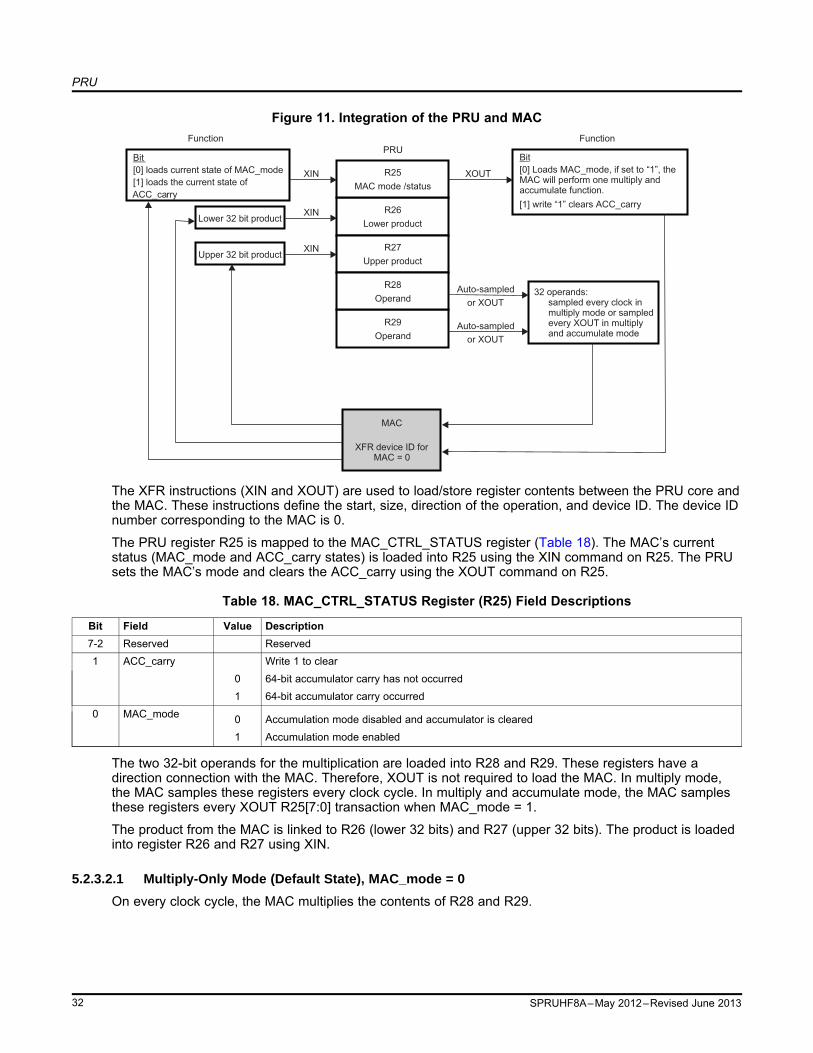
Auto-sampled
or XOUT
XOUT
MAC
XFR device ID forMAC = 0
R26
R27
R28
R29
XIN
Bit
[0] loads current state of MAC_mode
[1] loads the current state of
XINLower 32 bit product
XINUpper 32 bit product
R25
MAC mode /status
R26
R27
R28
R29
R25
MAC mode /status
R26
Lower product
R27
Upper product
R25
MAC mode /status
Bit
[0] Loads MAC_mode, if set to “1”, theMAC will perform one multiply andaccumulate function.
[1] write “1” clears ACC_carry
Auto-sampled
or XOUT
R29
Operand
R28
Operand32 operands:
sampled every clock inmultiply mode or sampledevery XOUT in multiplyand accumulate mode
Function Function
PRU
ACC_carry
PRU
Figure 11. Integration of the PRU and MAC
The XFR instructions (XIN and XOUT) are used to load/store register contents between the PRU core andthe MAC. These instructions define the start, size, direction of the operation, and device ID. The device IDnumber corresponding to the MAC is 0.
The PRU register R25 is mapped to the MAC_CTRL_STATUS register (Table 18). The MAC’s currentstatus (MAC_mode and ACC_carry states) is loaded into R25 using the XIN command on R25. The PRUsets the MAC’s mode and clears the ACC_carry using the XOUT command on R25.
Table 18. MAC_CTRL_STATUS Register (R25) Field Descriptions
Bit Field Value Description7-2 Reserved Reserved1 ACC_carry Write 1 to clear
0 64-bit accumulator carry has not occurred1 64-bit accumulator carry occurred
0 MAC_mode 0 Accumulation mode disabled and accumulator is cleared1 Accumulation mode enabled
The two 32-bit operands for the multiplication are loaded into R28 and R29. These registers have adirection connection with the MAC. Therefore, XOUT is not required to load the MAC. In multiply mode,the MAC samples these registers every clock cycle. In multiply and accumulate mode, the MAC samplesthese registers every XOUT R25[7:0] transaction when MAC_mode = 1.
The product from the MAC is linked to R26 (lower 32 bits) and R27 (upper 32 bits). The product is loadedinto register R26 and R27 using XIN.
5.2.3.2.1 Multiply-Only Mode (Default State), MAC_mode = 0
On every clock cycle, the MAC multiplies the contents of R28 and R29.
32 SPRUHF8A–May 2012–Revised June 2013

R28
32-bit operand
X
R29
32-bit operand
=
R27
Upper 32-bit product
R26
Lower 32-bit operand
MACXIN
Multiply and Accumulate mode:sampled every XOUT of R25
R28
32-bit operand
X
R29
32-bit operand
=
R27
Upper 32-bit product
R26
Lower 32-bit operand
MACXIN
Multiply mode:sampled every clock cycle
PRU
Figure 12. Multiply-Only Mode Functional Diagram
The following steps are performed by the PRU firmware for multiply-only mode:1. Enable multiply only MAC_mode.
• Clear R25[0] for multiply only mode.• Store MAC_mode to MAC using XOUT instruction on R25. For example: XOUT 0, R25, 1.
2. Load operands into R29 and R28.3. Load product into PRU using XIN instruction on R27, R26.
Repeat steps 2 and 3 for each new operand.
5.2.3.2.2 Multiply and Accumulate Mode, MAC_mode = 1
On every XOUT R25_reg[7:0] transaction, the MAC multiplies the contents of R28 and R29, adds theproduct to its accumulated result, and sets ACC_carry if an accumulation overflow occurs.
Figure 13. Multiply and Accumulate Mode Functional Diagram
The following steps are performed by the PRU firmware for multiply and accumulate mode:1. Enable multiply and accumulate MAC_mode.
• Set R25[1:0] = 1 for accumulate mode.• Store MAC_mode to MAC using XOUT instruction on R25. For example: XOUT 0, R25, 1.
2. Clear accumulator and carry flag.• Set R25[1:0] = 3 to clear accumulator.• Store accumlator to MAC using XOUT instruction on R25. For example: XOUT 0, R25, 1.
3. Load operands into R29 and R28.4. Multiply and accumulate, XOUT R25_reg[1:0] = 1
Repeat step 4 for each multiply and accumulate using same operands.Repeat step 3 and 4 for each multiply and accumulate for new operands.
5. Load the accumulated product into R27_reg, R26_reg and the ACC_carry status into R25_reg usingthe XIN instruction.
Note: Steps one and two are required to set the accumulator mode and clear the accumulator and carryflag.
33SPRUHF8A–May 2012–Revised June 2013

PRU0
R0R1R2…
R28R29
PRU1
R0R1R2…
R28R29
Bank0
R0R1R2…
R28R29
Bank1
R0R1R2…
R28R29
Bank2
R0R1R2…
R28R29
bro
adsid
ein
terf
ace
bro
adsid
e in
terf
ace
PRU
5.2.4 PRU0/1 Scratch PadThe PRU-ICSS supports a scratch pad with three independent banks accessible by the PRU cores. ThePRU cores interact with the scratch pad through broadside load/store PRU interface and XFR instructions.The scratch pad can be used as a temporary place holder for the register contents of the PRU cores.Direct connection between the PRU cores is also supported for transferring register contents directlybetween the cores.
5.2.4.1 Features
The PRU-ICSS scratch pad supports the following features:• Three scratch pad banks of 30, 32-bit registers (R29:0)• Flexible load/store options
– User-defined start byte and length of the transfer– Length of transfer ranges from one byte of a register to the entire register content (R29 to R0)– Simultaneous transactions supported between PRU0 ↔ Bank<n> and PRU1 ↔ Bank<m>– Direct connection of PRU0 → PRU1 or PRU1 → PRU0 for all registers R29–R0
• XFR instruction operate in one clock cycle• Optional XIN/XOUT shift functionality allows remapping of registers (R<n> → R<m>) during load/store
operation
Figure 14. Integration of PRU and Scratch Pad
5.2.4.2 Implementations and Operations
XFR instructions are used to load/store register contents between the PRU cores and the scratch padbanks. These instructions define the start, size, direction of the operation, and device ID. The device IDcorresponds to the external source or destination (either a scratch pad bank or the other PRU core). Thedevice ID numbers are shown in Table 19. Note the direct connect mode (device ID 14) can be used tosynchronize the PRU cores.
34 SPRUHF8A–May 2012–Revised June 2013

PRU
Table 19. Scratch Pad XFR IDDevice ID Function10 Selects Bank011 Selects Bank112 Selects Bank213 Reserved14 Selects other PRU core (Direct connect mode)
A collision occurs when two XOUT commands simultaneously access the same asset or device ID.Table 20 shows the priority assigned to each operation when a collision occurs. In direct connect mode(device ID 14), any PRU transaction will be terminated if the stall is greater than 1024 cycles. This willgenerate the event pr<1/0>_xfr_timeout that is connected to INTC.
Table 20. Scratch Pad XFR Collision ConditionsOperation Collision HandlingPRU<n> XOUT (→) bank[j] If both PRU cores access the same bank simultaneously, PRU0
is given priority. PRU1 will temporarily stall until the PRU0operation completes.
PRU<n> XOUT (→) PRU<m> If PRU<n> executes XOUT before PRU<m> executes XIN, thenPRU<n> will stall until either PRU<m> executes XIN or the stallis greater than 1024 cycles.
PRU<n> XIN (←) PRU<m> If PRU<n> executes XIN before PRU<m> executes XOUT, thenPRU<n> will stall until either PRU<m> executes XIN or the stallis greater than 1024 cycles.
5.2.4.2.1 Optional XIN/XOUT Shift
The optional XIN/XOUT shift functionality allows register contents to be remapped or shifted within thedestination’s register space. For example, the contents of PRU0 R6-R8 could be remapped to Bank1 R10-12. The XIN/XOUT shift feature is not supported for direct connect mode, only for transfers between aPRU core and scratch pad bank.
The shift feature is enabled or disabled through the SPP register of the PRU-ICSS CFG register space.When enabled, R0[4:0] (internal to the PRU) defines the number of 32-bit registers in which content isshifted in the scratch pad bank. Note that scratch pad banks do not have registers R30 or R31.
5.2.4.2.2 Example Scratch Pad Operations
The following PRU firmware examples demonstrate the shift functionality. Note these assume theSHIFT_EN bit of the SPP register of the PRU-ICSS CFG register space has been set.
XOUT Shift By 4 RegistersMOV R0.b0, 4XOUT 10, R4, 16 // Store R4:R7 to R8:R11 in bank0
XOUT Shift By 9 Registers, With Wrap AroundMOV R0.b0, 9XOUT 11, R25, 20 // Store R25:R29 to R4:R9 in bank1
XIN Shift By 10 RegistersMOV R0.b0, 10XIN 12, R4, 12 // Load R14:R16 from bank2 to R4:R6
35SPRUHF8A–May 2012–Revised June 2013

PRU
5.3 Basic Programming Model
5.3.1 PASM — PRU Assembler OverviewPASM is a command-line-driven assembler for the programmable real-time execution unit (PRU) of theprogrammable real-time unit subsystem (PRUSS). It is designed to build single executable images using aflexible source code syntax and a variety of output options. PASM is available for Windows and Linux.
5.3.1.1 Calling Syntax
The command line syntax to PASM is:pasm_2 -V3 [bcmldz] SourceFile [OutFileBasename] [-Dname=value] [-CArrayName]
Note that only the source file SourceFile is required on the command line. The assembler will default tooutput option "-c" which generates a C array containing the binary opcode data. The majority of the optionflags select a variety of output formats.
The output file OutFileBasename is a base name only. It defaults to the same name as the source file (forexample "myprog.p" would have a default base name of "myprog"). Standard filename extensions areapplied to the base name to create the final output filename(s), depending on the output option(s)selected.
When specifying PASM options, options can be specified individually or as a group. For example, either ofthe two invocations below is valid:pasm_2 -V3 -cdl myprog.ppasm_2 -V3 -c -d -l myprog.p
Filenames and options can also be mixed, for example:pasm_2 -V3 myprog.p -cdlpasm_2 -V3 -cd myprog.p -DMYVAL=1 -l
5.3.1.1.1 Output Formats
All program images start at Programmable Real-Time Unit (PRU) address 0. For example, if a programhas an internal origin of 8, the first eight 32 bit words of the program image output will be zero.
The following output options are supported. The output file name shown in the table is generatedassuming a base name of “myprog”:
Command Line Option Output Format Output Filename-b Little endian binary file myprog.bin-c C include file containing unsigned long myprog_bin.h
array called PRUcode[] (1)
-m Image file containing one 32 bit hex myprog.imgopcode per line
-L Listing file containing original source code myprog.txtand generated opcodes.
-l Listing file containing post-processed code myprog.lstand generated opcodes
-d Debugger output file (opcodes with source myprog.dbgand label info)
(1) The name “PRUcode[]” can be redefined using the –C option.
36 SPRUHF8A–May 2012–Revised June 2013

PRU
5.3.1.1.2 Additional Options
PASM supports some additional command line options that are not associated with output file format:
Command Line Option Function-V# PRU core version number. V3 for PRUSSv2.-C Rename the code array declared when using the -c option-D Constant definition-z Enable PASM assembler debug output
5.3.1.1.2.1 Rename the Code Array for the -c Option
By default, the –c option will create an output file with a name ending in “_bin.h”. Inside this createdinclude file, the output code is defined as a C array of 32 bit values. The default name of the array is“PRUcode[]”. The –C option allows the user to redefine this name to something more appropriate. Forexample the following command line will create an output file named “myprog_bin.h”, and the C arrayinside the created file will be called “MyProg_Release_003a[]”.pasm_2 -V3 -c myprog.p -CMyProg_Release_003a
5.3.1.1.2.2 Constant Definitions
When the “-D” option is specified, the remaining command line argument is interpreted as a constantassignment. For example, to add an assignment “1” to the constant “MYVAL”, any of the following is valid:pasm_2 -V3 -cdl myprog.p -DMYVAL=1pasm_2 -V3 -c -d -l -DMYVAL=1 myprog.ppasm_2 -V3 myprog.p -cdlDMYVAL=1
Since the default value assigned to a constant is “1”, the following is also equivalent:pasm_2 -V3 -c -d -l -DMYVAL myprog.p
Note that constants defined on the command line do not override constants defined in the source code.
5.3.2 PASM Source File SyntaxPASM is a non-linking two pass assembler. It assembles programs as a single monolithic image anddirectly generates executable code. As there is no linking stage in a PASM build, there are no section orsegment directives, nor memory maps or command files.
In PASM, there are four basic assembly operators. These include dot “.” commands, hash “#” commands,labels, and instructions (mnemonics). The user may supply comments that are invisible to the assembler.
5.3.2.1 Dot Commands
Dot commands are used to control the assembler, for example “.origin” and “.proc”. They can also be usedto declare complex data types as in the “.struct” directive.
5.3.2.1.1 Syntax
The rules for a dot command are as follows:• Must be the only assembly type on the line• Can be followed by a comment• Does not need to start in column 0
37SPRUHF8A–May 2012–Revised June 2013

PRU
5.3.2.1.2 Origin (.origin) Command
The origin command is used to specify a code offset in the PRU source file. Typically a single originstatement is specified before any instructions, but multiple origin commands can be specified in order toinsert space into the code map.
Example:.origin 8 // Start the next instruction at code offset 8
5.3.2.1.3 Entry Point (.entrypoint) Command
The entry point command is used to specify the code entry point to the debugger, and stores theinformation in the debug output file (*.dbg). It has no affect on any other output file type.
By default PASM will set the entry point to the first instruction generated by the assembly.
Examples:.entrypoint 0 // Set code entrypoint to address 0.entrypoint Start // Set code entrypoint to the code label "Start"
5.3.2.1.4 Set Call/Return Register (.setcallreg) Command
This command sets the call/return register that is used in the CALL and RET pseudo op instructions. If thiscommand is not specified, a default register of R30.w0 is used. This command must appear in the sourcecode prior to any program instructions, and it must specify a 16-bit register field.
Example:.setcallreg r15.w2 // Use R15.W2 in the CALL/RET pseudo ops
5.3.2.1.5 Start Macro Definition (.macro)
The .macro command is used to begin the definition of a macro. In the assembler, a macro can only beused in place of an opcode. There is always a single parameter to the command, being the name of themacro. Each macro section must start with a “.macro” and end with an “.endm”.
See Section 5.3.3.1 for more details on using macros.
Example:.macro mov32 // Define macro "mov32"
5.3.2.1.6 Specific Macro Parameter(s) (.mparam)
The .mparam command is used to add one or more parameters to a macro. The form of the command is:.mparam param1 [= default_value] [, param2 [= default_value] ]
When a parameter is given a default value, it is considered an optional parameter. Any optionalparameters must be the last parameters specified in the parameter list. It is acceptable to supply bothrequired and optional parameters on the same .mparam line.
See Section 5.3.3.1 for more details on using macros.
Example:.mparam dst, src // Define 2 required parameters, "dst" and "src".mparam temp = r0 // Define an optional parameter "temp" that
// defaults to the value 'r0'.
5.3.2.1.7 End Macro Definition (.endm)
The .endm command is used to complete the definition of a macro. It is required at the end of any macrospecification. There are no parameters.
See Section 5.3.3.1 for more details on using macros.
Example:.endm // Completed defining macro
38 SPRUHF8A–May 2012–Revised June 2013

PRU
5.3.2.1.8 Structure (.struct) Command
The structure command is used to open a declaration to a new structure in PASM. PASM uses structuresto generate standard equates, and allow the user to perform register allocation to private structureinstances.
See Section 5.3.3.2 for more details on using scope and structures.
Example:.struct myStruct // Declare a structure template called "myStruct"
5.3.2.1.9 End Structure (.ends) Command
The end structure command is used to close a structure declaration. PASM uses structures to generatestandard equates, and allow the user to perform register allocation to private structure instances.
See Section 5.3.3.2 for more details on using scope and structures.
Example:.ends
5.3.2.1.10 Field Directives (.u8, .u16, .u32)
Field directives are used within an open structure declaration to define fields within the structure.
See Section 5.3.3.2 for more details on using scope and structures.
Example:.struct MyStruct
.u32 MyInt // 32-bit field
.u16 MyShort // 16-bit field
.u8 MyByte1 // 8-bit field
.u8 MyByte2 // 8-bit field.ends
5.3.2.1.11 Assignment Directive (.assign)
The assignment directive is used to map a defined structure onto the PRU register file. An assignstatement can begin on any register boundary.
The programmer may declare the full assignment span manually (both starting and ending register), orleave the ending register blank. When the programmer declares a full register span, PASM will generatean error when the specified span is incorrect. This allows the programmer to formally map structures tospecific register spans, reducing the chance that register assignments will accidentally overlap.
Some structures will also require specific alignments due to how their fields are arranged within thestructure. PASM will generate an error if the structure alignment requirements can not be met with thespecified starting register.
See Section 5.3.3.2 for more details on using scope and structures.
Example:.assign MyStruct, R4, R5, MyName1 // Make sure this uses R4 thru R5.assign MyStruct, R6, *, MyName2 // Don’t need to validate the range
5.3.2.1.12 Enter New Variable Scope (.enter)
The .enter command is used to create and enter a new variable scope. There is a single parameter to thecommand that specifies the name of the scope. Any structures that are assigned inside a named scopecan only be accessed when the scope is open. Use of variable scopes is optional.
See Section 5.3.3.2 for more details on using scope and structures.
Example:.enter Scope1 // Create and enter scope named "Scope1"
39SPRUHF8A–May 2012–Revised June 2013

PRU
5.3.2.1.13 Leave a Variable Scope (.leave)
The .leave command is used to leave a specific variable scope. There is a single parameter to thecommand that specifies the name of the scope to leave. Scopes do not need to be entered or left in anyparticular order, but a natural ordering can be enforced by the programmer.
See Section 5.3.3.2 for more details on using scope and structures.
Example:.enter Scope1 // Create and enter scope named "Scope1"
.enter Scope2 // Create and enter scope named "Scope2"
.leave Scope2 // Leave scope named "Scope2".leave Scope1 // Leave scope named "Scope1"
5.3.2.1.14 Referencing an Existing Variable Scope (.using)
The .using command is used to enter a specific variable scope that has been previously created and left.There is a single parameter to the command that specifies the name of the scope to enter. The .leavecommand is then used to leave the scope after being entered with .using.
See Section 5.3.3.2 for more details on using scope and structures.
Example:.using Scope1 // Enter existing scope named "Scope1"
.using Scope2 // Enter existing scope named "Scope2"
.leave Scope2 // Leave scope named "Scope2".leave Scope1 // Leave scope named "Scope1"
5.3.2.2 Hash Commands
Hash commands are used to control the assembler pre-processor. They are quite similar to their Ccounterparts.
5.3.2.2.1 Syntax
The rules for a hash command are as follows:• Must be the only assembly type on the line• Can be followed by a comment• Does not need to start in column 0
5.3.2.2.2 Include (#include) Command
The #include command is used to include additional source files in the assembly process. When a“#include” is specified, the included file is immediately opened, parsed, and processed.
The calling syntax for #include can use quotes ‘” “’ or brackets “< >". Specifying quotes is functionallyequivalent to specifying brackets. For example:#include "localInclude.h"
#include "c:\include\myInclude.h"
#include <inc\myInclude.h>
As PASM uses a monolithic single source approach, the #include statement can be used to specifyexternal source files. This allows a developer to break up a complicated application into several smallersource files.
For example, an application may consist of a master source file “myApp.p” which itself contains nothingbut include commands for including sub source files. The contents of “myApp.p” may appear as follows:#include "myInitialization.p"#include "myMainLoop.p"#include "mySubroutines.p"
40 SPRUHF8A–May 2012–Revised June 2013

PRU
The above lines would include each source file in turn, concatenating one after the other in the final codeimage. Each of these included source files may have additional include files of their own.
Including the same include file multiple times will not result in an error, however including files recursivelywill result in an error.
5.3.2.2.3 Define (#define) Command
The “#define” command is used to specify a simple text substitution. Any text defined in a #define issubstituted for the defined name within the code.
For example, if the programmer writes:#define BUFFER_ADDRESS 0x08001000
ldi r1.w0, BUFFER_ADDRESS & 0xFFFFldi r1.w2, BUFFER_ADDRESS >> 16
This would load 0x1000 into register r1.w0 and then 0x0800 into register r1.w2.
Equates are expanded recursively, so the value of the define does not need to be resolved until it is used.For example:#define B A#define A 1
ldi r1, B
The above will load “1” in register r1.
5.3.2.2.4 Undefine (#undef) Command
The “#undef” command is used to undefined a constant that was previously assigned via #define.
For example:// Redefine our buffer address without generating an assmbler warning#undef BUFFER_ADDRESS#define BUFFER_ADDRESS 0x08001000
5.3.2.2.5 Error (#error) Command
The “#error” command is used to specify an error during assembly. For example, if the programmerwishes to verify the constant value MYMODE is defined, they can write:#ifndef MYMODE#error Mode not specified#endif
The above will produce an error if the program is assembled and MYMODE is not defined.
5.3.2.2.6 Warning (#warn) Command
The “#warn” command is used to specify a warning during pass 1 of the assembly. For example, if theprogrammer wishes to verify the constant value MYMODE is defined, but still allow a default mode, theycan write:#ifndef MYMODE#warn Mode not specified - setting default#define MYMODE DEFAULT_MODE#endif
The above will produce an assembler warning if the program is assembled and MYMODE is not defined.
41SPRUHF8A–May 2012–Revised June 2013

PRU
5.3.2.2.7 Notation (#note) Command
The “#note” command is used to specify a notation during pass 1 of the assembly. For example, if theprogrammer wishes to allow a default setting of the constant value MYMODE, but still notify theprogrammer what is happening, they can write:#ifndef MYMODE#note Using default MYMODE#define MYMODE DEFAULT_MODE#endif
The above will produce an assembler notation if the program is assembled and MYMODE is not defined,but it is not counted as an error or a warning.
5.3.2.2.8 If Defined (#ifdef) Command
The “#ifdef” command is used to specify a block of conditional code based on whether the suppliedconstant is defined. Here, the code inside the #ifdef block will be assembled only if the constant is defined,regardless of its defined value. Every #ifdef must be followed by a #endif. For example:#define MYVAL 1#ifdef MYVAL
// This code in this block will be assembled#endif
#undef MYVAL#ifdef MYVAL
// This code in this block will NOT be assembled#endif
5.3.2.2.9 If Not Defined (#ifndef) Command
The “#ifndef” command is used to specify a block of conditional code based on whether the suppliedconstant is defined. Here, the code inside the #ifndef block will be assembled only if the constant is notdefined. Every #ifndef must be followed by a #endif. For example:#define MYVAL 1#ifndef MYVAL
// This code in this block will NOT be assembled#endif
#undef MYVAL#ifndef MYVAL
// This code in this block will be assembled#endif
5.3.2.2.10 End If (#endif) Command
The “#endif” command is used to close a previously open #ifdef or #ifndef, thus closing the conditionalassembly block.
5.3.2.2.11 Else (#else) Command
The “#else” command is used to specify a block of conditional code based on a previous #ifdef or #ifndef,allowing for the opposite case. For example:#define MYVAL 1#ifdef MYVAL
// This code in this block will be assembled#else
// This code in this block will NOT be assembled#endif
42 SPRUHF8A–May 2012–Revised June 2013

PRU
5.3.2.3 Labels
Labels are used denote program addresses. When placed at the beginning of a source line andimmediately followed by a colon ‘:’, they mark a program address location. When referenced by aninstruction, the corresponding marked address is substituted for the label.
The syntax rules for labels are as follows:• A label definition must be immediately followed by a colon.• Only instructions and/or comments can occupy the same source line as a label.• Labels can use characters ‘A’-‘Z’, ‘a’-‘z’, ‘0’-‘9’ plus underscores ‘_’ and dots ‘.’.• A label can not begin with a number (‘0’-‘9’).
The following illustrates defining and using the label named “loop_label”:ldi r0, 100
loop_label:sub r0, r0, 1qbne loop_label, r0, 0ret
5.3.2.4 Comments
In PASM comments are transparent to all other operations, thus they can appear anywhere on any sourceline. However, since comments are terminated by the end of line, they are by definition, the last field on aline.
The syntax rules for comments are as follows:• Comments must be preceded by '//'.• Comments are always the last field to appear on a line.
The following illustrates defining a comment://-------------------------// This is a comment//-------------------------ldi r0, 100 // This is a comment
5.3.2.5 PRU Assembly Instructions
Instruction lines include a PRU mnemonic, followed by a list of parameters appropriate for the mnemonic.See Section 5.3.4, PRU Instruction Set, for supported instructions. Note that some of these are pseudoops, which do not affect their use, but may affect how they are displayed when disassembled by adebugger.
5.3.2.5.1 Syntax
An instruction line consists of a mnemonic is followed by a specific number of parameters appropriate forthe instruction. Parameters are always separated by commas. For example:mnemonic parameter1, parameter2, parameter3, parameter4
Each instruction accepts either a fixed or varying number of parameters. Those that use a varying numberof parameters do so for either flexibility in formatting, or to adjust to different use cases. In most cases, atleast one of the parameters can be one of a couple different types. For example, on many instructions thethird parameter can be either a register or an immediate value.
All parameters take the form a register, label, or immediate value. There exists both a formal and informalsyntax for instruction lines. The formal syntax was inherited from an earlier assembler. Modernapplications typically use the informal syntax. These are discussed in more detail later in section dealingwith parameter type, but here are some examples of both formal and informal syntax.
43SPRUHF8A–May 2012–Revised June 2013

PRU
Formal Syntax:LDI R2, #5LDI R3, #3ADD R1, R2, R3QBNE (LABEL), R1, #8JMP (LABEL)
Informal Syntax:ldi r2, 5ldi r3, 3add r1, r2, r3qbne label, r1, 8jmp label
5.3.2.5.2 Registers
The PASM assembler treats PRU registers as bit fields within the register file. All registers start with abase register (R0 through R31). A base register defines an unsigned 32 bit quantity. This 32 bit base fieldcan be modified by appending different register modifier suffixes. The modifier suffix selects which portionof the register on which to operate. The suffixes are as follows:
Suffix Range of n Meaning.wn 0 to 2 16 bit field with a byte offset of n within
the parent field.bn 0 to 3 8 bit field with a byte offset of n within the
parent field.tn 0 to 31 1 bit field with a bit offset of n within the
parent field
Multiple suffixes may appear on a base register to further modify the desired field. For example:
Register MeaningR5 32 bit value, bits 0 to 32 of register R5
R5.w0 16 bit value, bits 0 to 15 of register R5R5.w1 16 bit value, bits 8 to 23 of register R5R5.b1 8 bit value, bits 8 to 15 of register R5R5.t7 1 bit value, bit 7 of register R5
R5.w1.b1 8 bit value, bits 8 to 15 of “R5.w1”(this corresponds to bits 16 to 23 of register R5)
R5.w1.b1.t7 1 bit value, bit 7 of R5.w1.b1(since R5.w1.b1 is bits 16 to 23 of R5, this is bit 23 of registerR5)
Note that some suffix combinations are illegal. A combination is illegal when a modifier attempts to extracta field that is not contained in the parent field. For example:
Illegal Register Reason for IllegalityR5.t0.b0 A byte field can be extracted from a single bit fieldR5.w2.b2 Bits 16 to 23 can not be extracted out of a 16 bit fieldR5.b0.t8 Bit 8 can not be extracted out of an 8 bit field
R5.w0.w1 Bits 8 to 23 can not be extracted out of a 16 bit field. Note thatR5.w1.w0 would be legal, but not of much use as R5.w1.w0 ==R5.w1
44 SPRUHF8A–May 2012–Revised June 2013

PRU
5.3.2.5.3 Loop/Byte Count Registers
Register R0 is used in some instructions to specify a loop count or byte count value. A count of this type isalways the last parameter in the parameter list. A loop/byte count is always an 8 bit sub-field of R0. Forlegacy reasons, the register is expressed only by its modifier suffix. For example: “b0” is taken to mean“R0.b0” and “b2” is taken to mean “R0.b2”.
Register loop/byte counts are allowed only in very specific circumstances which are detailed in theappropriate instruction description.
5.3.2.5.4 Labels
Labels are used to reference code locations in a program. In PASM, labels are used to specify targets ofjump instructions, but can also be used in an instruction that calls for an immediate value (so long as thelabel’s value fits in the immediate field’s specified bit width). When specifying a label, the user has theoption of enclosing it in parenthesis “( )” for legacy concerns, but it is not required or recommended. Forexample:
QBNE (MyLabel), R1, #8JMP (MyLabel)LDI R1.W0, #MyLabelqbne MyLabel, r1, 8jmp MyLabelldi r1.w0, MyLabel
5.3.2.5.5 Immediate Values
Immediate values are simple numbers or expressions that compute to constant values. Immediate valuesor expressions can be preceded by a hash character ‘#’ for legacy concerns, but this is not required orrecommended. For example:
LDI R1, #0x25and r2, r1, 0b1001011ldi r1.w0, 0x12345678 & 0xFFFFldi r1.w2, 0x12345678 >> 16add r2, r3, (6*(5-3)/2) << 2
Note that if an immediate value is lead by a ‘0’ without a format notation of ‘x’ or ‘b’, then the base isassumed to be in octal format.
5.3.2.5.6 Syntax Terms and Definitions
The following terms are definitions are used to specify parameters in a formal instruction definition.
Field Name Meaning ExamplesREG, REG1, REG2, … Any register field from 8 to 32 bits r0
r1.w0r3.b2
Rn, Rn1, Rn2, … Any 32 bit register field (r0 through r31) r0r1
Rn.tx Any 1 bit register field (x denotes the bit r0.t23position) r1.b1.t4
Cn, Cn1, Cn2, … Any 32 bit constant register entry (c0 c0through c31) c1
bn Specifies a field that must be b0, b1, b2, b0or b3 – denoting r0.b0, r0.b1, r0.b2, andr0.b3 respectively.
LABEL Any valid label, specified with or without loop1parenthesis. An immediate value denoting (loop1)an instruction address is also acceptable. 0
IM(n) An immediate value from 0 to n. #23Immediate values can be specified with or 0b0110without a leading hash “#” character. 2+2Immediate values, labels, and register &r3.w2addresses are all acceptable.
45SPRUHF8A–May 2012–Revised June 2013

PRU
Field Name Meaning ExamplesOP(n) This is a combination (or the union) of r0
REG and IM(n). It specifies a register field r1.w0from 8 to 32 bits, or an immediate value #0x7Ffrom 0 to n. A label or register address 1<<3that resolves to a value within the denoted loop1range is also acceptable. &r1.w0
For example the following is the definition for the ADD instruction:ADD REG1, REG2, OP(255)
This means that the first and second parameters can be any register field from 8 to 32 bits. The thirdparameter can be any register field from 8 to 32 bits or an immediate value from 0 to 255. Thus thefollowing are all legal ADD instructions:
ADD R1, R1, #0x25 // r1 += 37ADD r1, r1, 0x25 // r1 += 37ADD r3, r1, r2 // r3 = r1 + r2ADD r1.b0, r1.b0, 0b100 // r1.b0 += 4ADD r2, r1.w0, 1<<3 // r2 = r1.w0 + 8
5.3.3 Advanced Topics
5.3.3.1 Using Macros
Macros are used to define custom instructions for the CPU. They are similar to in-line subroutines in C.
5.3.3.1.1 Defining a Macro
A macro is defined by first declaring the start of a macro block and specifying the macro name, thenspecifying the assembly code to implement the intended function, and finally closing the macro block.
.macro macro name
.mparam macro parameters< lines of assembly code >< lines of assembly code >< lines of assembly code >
.endm
The assembly code within a macro block is identical to that used outside a macro block with minorvariances:• Macros cannot be nested• No dot commands may appear within a macro block other than “.mparam”.• Pre-processor definitions and conditional assembly are processed when the macro is defined.• Structure references are expanded when the macro is used.• Labels defined within a macro are considered local and can only be referenced from within the macro.• References to external labels from within a macro are allowed.
46 SPRUHF8A–May 2012–Revised June 2013

PRU
5.3.3.1.2 Macro Parameters
The macro parameters can be specified on one “.mparam” line or multiple. They are processed in theorder that they are encountered. There are two types of parameters, mandatory and optional. Optionalparameters are assigned a default value that is used in the event that they are not specified when themacro is used. Since parameters are always processed in order, any optional parameters must come last,and once an optional parameter is used, none of the remaining parameters may be specified.
For example:.macro mv1 // Define macro "mv1".mparam dst=r0, src=5 // Two optional parameters
mov dst, src.endm
For the above macro, the following expansions are possible:
Macro Invocation Resultmv1 r1, 7 mov r1, 7mv1 r2 mov r2, 5mv1 mov r0, 5
Note that optional parameters can not be passed by using “empty” delimiters. For example, the followinginvocation of “mv1” is illegal:
mv1 , 7 // Illegal attempt to do ‘mov r0, 7’
5.3.3.1.3 Example Macros
5.3.3.1.3.1 Example 1: Move 32-bit Value (mov32)
The mov32 macro is a good example of a simple macro that saves some typing and makes a source codelook a little cleaner.
Note: The latest assembler supports 32-bit immediate values natively, making this MACRO undesirablefor general use (but it makes a good macro example).
Specification://// mov32 : Move a 32bit value to a register//// Usage:// mov32 dst, src//// Sets dst = src. Src must be a 32 bit immediate value.//.macro mov32.mparam dst, src
mov dst.w0, (src) & 0xFFFFmov dst.w2, (src) >> 16
.endm
Example Invocation:The invocation for this macro is the same as the standard mov pseudo op:
mov32 r0, 0x12345678
Example Expansion:The expansion of the above invocation uses to immediate value moves to accomplish the 32-bit load.
mov r0.w0, (0x12345678) & 0xFFFFmov r0.w2, (0x12345678) >> 16
47SPRUHF8A–May 2012–Revised June 2013

PRU
5.3.3.1.3.2 Example 2: Quick Branch If in Range (qbir)
Any label defined within a macro is altered upon expansion to be unique. Thus internal labels are local tothe macro and code defined outside of a macro cannot make direct use of a label that is defined inside amacro. However code contained within a macro can make free use of externally defined labels.
The qbir macro is a simple example that uses a local label. The macro instruction will jump to the suppliedlabel if the test value is within the specified range.
Specification://// qbir : Quick branch in range//// Usage:// qbir label, test, low, high//// Jumps to label if (low <= test <= high).// Test must be a register. Low and high can be// a register or a 8 bit immediate value.//.macro qbir.mparam label, test, low, high
qbgt out_of_range, test, lowqbge label, test, high
out_of_range:.endm
Example Invocation:The example below checks the value in R5 for membership of two different ranges. Note that the range“low” and “high” values could also come from registers. They do not need to be immediate values:
qbir range1, r5, 1, 9 // Jump if (1 <= r5 <= 9)qbir range2, r5, 25, 50 // Jump if (25 <= r5 <= 50)
Example Expansion:The expansion of the above invocation illustrates how external labels are used unmodified while internallabels are altered on expansion to make them unique.
qbgt _out_of_range_1_, R5, 1qbge range1, r5, 9
_out_of_range_1_:qbgt _out_of_range_2_, R5, 25qbge range2, r5, 50
_out_of_range_2_:
48 SPRUHF8A–May 2012–Revised June 2013

PRU
5.3.3.2 Using Structures and Scope
5.3.3.2.1 Basic Structures
Structures are used in PASM to eliminate the tedious process of defining structure offset fields for using inLBBO/SBBO, and the even more painful process of mapping structures to registers.
5.3.3.2.1.1 Declaring Structure Types
Structures are declared in PASM using the “.struct” dot command. This is similar to using a “typedef” in C.PASM automatically processes each declared structure template and creates an internal structure type.The named structure type is not yet associated with any registers or storage. For example, say theapplication programmer has the following structure in C:typedef struct _PktDesc {
struct _PktDesc *pNext;char *pBuffer;unsigned short Offset;unsigned short BufLength;unsigned short Flags;unsigned short PktLength;
} PKTDESC;
The equivalent PASM structure type is created using the following syntax:.struct PktDesc
.u32 pNext
.u32 pBuffer
.u16 Offset
.u16 BufLength
.u16 Flags
.u16 PktLength.ends
5.3.3.2.1.2 Assigning Structure Interfaces to Registers
The second function of the PASM structure is to allow the application developer to map structures onto thePRU register file without the need to manually allocate registers to each field. This is done through the“.assign” dot command. For example, say the application programmer performs the following assignment:
.assign PktDesc, R4, R7, RxDesc // Make sure this uses R4 thru R7
When PASM sees this assignment, it will perform three tasks for the application developer:1. PASM will verify that the structure perfectly spans the declared range (in this case R4 through R7).
The application developer can avoid the formal range declaration by substituting ‘*’ for ‘R7’ above.2. PASM will verify that all structure fields are able to be mapped onto the declared range without any
alignment issues. If an alignment issue is found, it is reported as an error along with the field inquestion. Note that assignments can begin on any register boundary.
3. PASM will create an internal data type named “RxDesc”, which is of type “PktDesc”.
For the above assignment, PASM will use the following variable equivalencies. Note that PASM willautomatically adjust for endian mode.
Variable Little EndianRxDesc R4RxDesc.pNext R4RxDesc.pBuffer R5RxDesc.Offset R6.w0RxDesc.BufLength R6.w2RxDesc.Flags R7.w0RxDesc.PktLength R7.w2
49SPRUHF8A–May 2012–Revised June 2013

PRU
For example the source line below will be converted to the output shown:// Input Source LineADD r20, RxDesc.pBuffer, RxDesc.Offset
// Output Source LineADD r20, R5, R6.w0
5.3.3.2.2 SIZE and OFFSET Operators
SIZE and OFFSET are two useful operators that can be applied to either structure types or structureassignments. The SIZE operator returns the byte size of the supplied structure or structure field. TheOFFSET operator returns the byte offset of the supplied field from the start of the structure.
5.3.3.2.2.1 SIZE Operator Example
Using the assignment example from the previous section, the following SIZE equivalencies would apply:
Variable Operation ResultsSIZE(PktDesc) 16SIZE(PktDesc.pNext) 4SIZE(PktDesc.pBuffer) 4SIZE(PktDesc.Offset) 2SIZE(PktDesc.BufLength) 2SIZE(PktDesc.Flags) 2SIZE(PktDesc.PktLength) 2SIZE(RxDesc) 16SIZE(RxDesc.pNext) 4SIZE(RxDesc.pBuffer) 4SIZE(RxDesc.Offset) 2SIZE(RxDesc.BufLength) 2SIZE(RxDesc.Flags) 2SIZE(RxDesc.PktLength) 2
5.3.3.2.2.2 OFFSET Operator Example
Using the assignment example from the previous section, the following OFFSET equivalencies wouldapply:
Variable Operation ResultsOFFSET(PktDesc) 0OFFSET(PktDesc.pNext) 0OFFSET(PktDesc.pBuffer) 4OFFSET(PktDesc.Offset) 8OFFSET(PktDesc.BufLength) 10OFFSET(PktDesc.Flags) 12OFFSET(PktDesc.PktLength) 14OFFSET(RxDesc) 0OFFSET(RxDesc.pNext) 0OFFSET(RxDesc.pBuffer) 4OFFSET(RxDesc.Offset) 8OFFSET(RxDesc.BufLength) 10OFFSET(RxDesc.Flags) 12OFFSET(RxDesc.PktLength) 14
50 SPRUHF8A–May 2012–Revised June 2013

PRU
5.3.3.2.3 Using Variable Scopes
On larger PASM applications, it is common for different structures to be applied to the same register rangefor use at different times in the code. For example, assume the programmer uses three structures, onecalled “global”, one called “init” and one called “work”. Assume that the global structure is always valid, butthat the init and work structures do not need to be used at the same time.
The programmer could assign the structures as follows:.assign struct_global, R2, R8, myGlobal.assign struct_init R9, R12, init // Registers shared with "work".assign struct_work R9, R13, work // Registers shared with "init"
The program code may look something like the following:
Start:
call InitGlobalData
Using R9 to R12 for "init" structuremov init.suff, myGlobal.data
call InitProcessing
qbbs InitComplete, init.flags.fComplete
DoWork:
call LoadWorkRecord
Using R9 to R13 for "work" structuremov r0, myGlobal.Status
qbeq type1, work.type, myGlobal.WorkType1
...
InitProcessing:
mov init.start, init.stuff
Using R9 to R12 for "init" structureset init.flags.fComplete
ret
The code has been shaded to emphasize when the shared registers are being used for the “init” structureand when they are been used for the “work” structure. The above is quite legal, but in this example, PASMdoes not provide any enforcement for the register sharing. For example, assume the work section of thecode contained a reference to the “init” structure:
DoWork:
call LoadWorkRecord
mov r0, myGlobal.Status
The reference to "init" would not cause anset init.flags.fWorkStarted assembly error.
qbeq type1, work.type, myGlobal.WorkType1
...
The above example would not result in an assembly error even though using the same registers for twodifferent purposes at the same time would result in a functional error.
51SPRUHF8A–May 2012–Revised June 2013

PRU
To solve this potential problem, named variable scopes can be defined in which the register assignmentsare to be made. For example, the above shared assignments can be revised to as shown below to includethe creation of variable scopes:.assign struct_global, R2, R8, myGlobal // Available in all scopes
.enter Init_Scope // Create new scope Init_Scope.assign struct_init R9, R12, init // Only available in Init_Scope
.leave Init_Scope // Leave scope Init_Scope
.enter Work_Scope // Create new scope Work_Scope.assign struct_work R9, R13, work // Only available in Work_Scope
.leave Work_Scope // Leave scope Work_Scope
Once the scopes have been defined, the structures assigned within can only be accessed while the scopeis open. Previously defined scopes can be reopened via the “.using” command.
.using Init_Scope
Start:
call InitGlobalData
Using "Init_Scope"mov init.suff, myGlobal.data
call InitProcessing
qbbs InitComplete, init.flags.fComplete
.leave Init_Scope
.using Work_Scope
DoWork:
call LoadWorkRecord
Using "Work_Scope"mov r0, myGlobal.Status
qbeq type1, work.type, myGlobal.WorkType1
...
.leave Work_Scope
.using Init_Scope
InitProcessing:
mov init.start, init.stuff
Using "Init_Scope"set init.flags.fComplete
ret
.leave Init_Scope
When using scopes as in the above example, any attempted reference to a structure assignment madeoutside a currently open scope will result in an assembly error.
5.3.3.3 Register Addressing and Spanning
Certain PRU instructions act upon or affect more than a single register field. These include MVIx, ZERO,SCAN, LBxO, and SBxO. It is important to understand how register fields are packed into registers, andhow these fields are addressed when using one of these PRU functions.
5.3.3.3.1 Little Endian Register Mapping
The registers of the PRU are memory mapped with the little endian byte ordering scheme. For example,say we have the following registers set to the given values:
R0 = 0x80818283
R1 = 0x84858687
Table 21 is the register mapping to byte offset in little endian:
52 SPRUHF8A–May 2012–Revised June 2013

PRU
Table 21. Register Byte Mapping in Little EndianByte Offset 0 1 2 3 4 5 6 7Register R0.b0 R0.b1 R0.b2 R0.b3 R1.b0 R1.b1 R1.b2 R1.b3FieldExample 0x83 0x82 0x81 0x80 0x87 0x86 0x85 0x84Value
There are three factors affected by register mapping and little endian mapping. There are register spans,the first byte affected in a register field, and register addressing. In addition, there are some alterations inPRU opcode encoding.
5.3.3.3.1.1 Register Spans
The concept of how the register file is spanned can be best viewed using the tables created in theexample from section 3.3.1. Registers are spanned by incrementing the byte offset from the start of theregister file for each subsequent byte.
For example assume we have the following registers set to their indicated values:
R0 = 0x80818283
R1 = 0x84858687
R2 = 0x00001000
If the instruction “SBBO R0.b2, R2, 0, 5” is executed, it will result in a memory write to memory address0x1000 as shown in little endian:
Table 22. SBBO Result for Little Endian ModeByte Address 0x1000 0x1001 0x1002 0x1003 0x1004Value 0x81 0x80 0x87 0x86 0x85
5.3.3.3.1.2 First Byte Affected
The first affected byte in a register field is literally the first byte to be altered when executing a PRUinstruction. For example, in the instruction “LBBO R0, R1, 0, 4”, the first byte to be affected by the LBBOis R0.b0 in little endian. The width of a field in a register span operation is almost irrelevant in little endian,since the first byte affected is independent of field width. For example, consider the following table:
Table 23. First Byte Affected in Little Endian ModeRegister Expression First Byte AffectedR0 R0.b0R0.w0 R0.b0R0.w1 R0.b1R0.w2 R0.b2R0.b0 R0.b0R0.b1 R0.b1R0.b2 R0.b2R0.b3 R0.b3
As can be seen in the table above, for any expression the first byte affected is always the byte offset ofthe field within the register. Thus in little endian, the expressions listed below all result in identicalbehavior.• LBBO R0, R1, 0, 4• LBBO R0.w0, R1, 0, 4• LBBO R0.b0, R1, 0, 4
53SPRUHF8A–May 2012–Revised June 2013

PRU
5.3.3.3.1.3 Register Address
The MVIx, ZERO, SCAN, LBxO, and SBxO instructions may use or require a register address instead ofthe direct register field in the instruction. In the assembler a leading ‘&’ character is used to specify that aregister address is to be used. The address of a register is defined to be the byte offset within the registerfile of the first affected byte in the supplied field.
Given the information already presented in this chapter, it should be straight forward to verify the followingregister address mappings:
Table 24. Register Addressing in Little EndianRegister Address Expression Little Endian
First Byte Affected Register Address&Rn Rn.b0 (n*4)&Rn.w0 Rn.b0 (n*4)&Rn.w1 Rn.b1 (n*4) + 1&Rn.w2 Rn.b2 (n*4) + 2&Rn.b0 Rn.b0 (n*4)&Rn.b1 Rn.b1 (n*4) + 1&Rn.b2 Rn.b2 (n*4) + 2&Rn.b3 Rn.b3 (n*4) + 3
Register addresses are very useful for writing endian agnostic code, or for overriding the declared fieldwidths in a structure element.
5.3.3.3.1.4 PRU Opcode Generation
The PRU binary opcode formats for LBBO, SBBO, LBCO, and SBCO use a byte offset for thesource/destination register in the PRU register file. For example, only the following destination fields canactually be encoded into a PRU opcode for register R1:• LBBO R1.b0, R0, 0, 4• LBBO R1.b1, R0, 0, 4• LBBO R1.b2, R0, 0, 4• LBBO R1.b3, R0, 0, 4
54 SPRUHF8A–May 2012–Revised June 2013

PRU
5.3.4 PRU Instruction Set
5.3.4.1 Arithmetic and Logical
All operations are 32 bits wide (with a 33-bit result in the case of arithmetic). The source values are zeroextended prior to the operation. If the destination is too small to accept the result, the result is truncated.
On arithmetic operations, the first bit to the right of the destination width becomes the carry value. Thus ifthe destination register is an 8 bit field, bit 8 of the result becomes the carry. For 16 and 32 bitdestinations, bit 16 and bit 32 are used as the carry bit respectively.
5.3.4.1.1 Unsigned Integer Add (ADD)
Performs 32-bit add on two 32 bit zero extended source values.
Definition:ADD REG1, REG2, OP(255)
Operation:REG1 = REG2 + OP(255)carry = (( REG2 + OP(255) ) >> bitwidth(REG1)) & 1
Example:add r3, r1, r2add r3, r1.b0, r2.w2add r3, r3, 10
5.3.4.1.2 Unsigned Integer Add with Carry (ADC)
Performs 32-bit add on two 32 bit zero extended source values, plus a stored carry bit.
Definition:ADC REG1, REG2, OP(255)
Operation:REG1 = REG2 + OP(255) + carrycarry = (( REG2 + OP(255) + carry ) >> bitwidth(REG1)) & 1
Example:adc r3, r1, r2adc r3, r1.b0, r2.w2adc r3, r3, 10
5.3.4.1.3 Unsigned Integer Subtract (SUB)
Performs 32-bit subtract on two 32 bit zero extended source values.
Definition:SUB REG1, REG2, OP(255)
Operation:REG1 = REG2 - OP(255)carry = (( REG2 - OP(255) ) >> bitwidth(REG1)) & 1
Example:sub r3, r1, r2sub r3, r1.b0, r2.w2sub r3, r3, 10
55SPRUHF8A–May 2012–Revised June 2013

PRU
5.3.4.1.4 Unsigned Integer Subtract with Carry (SUC)
Performs 32-bit subtract on two 32 bit zero extended source values with carry (borrow).
Definition:SUC REG1, REG2, OP(255)
Operation:REG1 = REG2 - OP(255) - carrycarry = (( REG2 - OP(255) - carry ) >> bitwidth(REG1)) & 1
Example:suc r3, r1, r2suc r3, r1.b0, r2.w2suc r3, r3, 10
5.3.4.1.5 Reverse Unsigned Integer Subtract (RSB)
Performs 32-bit subtract on two 32 bit zero extended source values. Source values reversed.
Definition:RSB REG1, REG2, OP(255)
Operation:REG1 = OP(255) - REG2carry = (( OP(255) - REG2 ) >> bitwidth(REG1)) & 1
Example:rsb r3, r1, r2rsb r3, r1.b0, r2.w2rsb r3, r3, 10
5.3.4.1.6 Reverse Unsigned Integer Subtract with Carry (RSC)
Performs 32-bit subtract on two 32 bit zero extended source values with carry (borrow). Source valuesreversed.
Definition:RSC REG1, REG2, OP(255)
Operation:REG1 = OP(255) - REG2 - carrycarry = (( OP(255) - REG2 - carry ) >> bitwidth(REG1)) & 1
Example:rsc r3, r1, r2rsc r3, r1.b0, r2.w2rsc r3, r3, 10
5.3.4.1.7 Logical Shift Left (LSL)
Performs 32-bit shift left of the zero extended source value.
Definition:LSL REG1, REG2, OP(31)
Operation:REG1 = REG2 << ( OP(31) & 0x1f )
Example:lsl r3, r3, 2lsl r3, r3, r1.b0lsl r3, r3.b0, 10
56 SPRUHF8A–May 2012–Revised June 2013
PRU
5.3.4.1.8 Logical Shift Right (LSR)
Performs 32-bit shift right of the zero extended source value.
Definition:LSR REG1, REG2, OP(31)
Operation:REG1 = REG2 >> ( OP(31) & 0x1f )
Example:lsr r3, r3, 2lsr r3, r3, r1.b0lsr r3, r3.b0, 10
5.3.4.1.9 Bitwise AND (AND)
Performs 32-bit logical AND on two 32 bit zero extended source values.
Definition:AND REG1, REG2, OP(255)
Operation:REG1 = REG2 & OP(255)
Example:and r3, r1, r2and r3, r1.b0, r2.w2and r3.b0, r3.b0, ~(1<<3) // Clear bit 3
5.3.4.1.10 Bitwise OR (OR)
Performs 32-bit logical OR on two 32 bit zero extended source values.
Definition:OR REG1, REG2, OP(255)
Operation:REG1 = REG2 | OP(255)
Example:or r3, r1, r2or r3, r1.b0, r2.w2or r3.b0, r3.b0, 1<<3 // Set bit 3
5.3.4.1.11 Bitwise Exclusive OR (XOR)
Performs 32-bit logical XOR on two 32 bit zero extended source values.
Definition:XOR REG1, REG2, OP(255)
Operation:REG1 = REG2 ^ OP(255)
Example:xor r3, r1, r2xor r3, r1.b0, r2.w2xor r3.b0, r3.b0, 1<<3 // Toggle bit 3
57SPRUHF8A–May 2012–Revised June 2013
PRU
5.3.4.1.12 Bitwise NOT (NOT)
Performs 32-bit logical NOT on the 32 bit zero extended source value.
Definition:NOT REG1, REG2
Operation:REG1 = ~REG2
Example:not r3, r3not r1.w0, r1.b0
5.3.4.1.13 Copy Minimum (MIN)
Compares two 32 bit zero extended source values and copies the minimum value to the destinationregister.
Definition:MIN REG1, REG2, OP(255)
Operation:if( OP(255) > REG2 )
REG1 = REG2;else
REG1 = OP(255);
Example:min r3, r1, r2min r1.w2, r1.b0, 127
5.3.4.1.14 Copy Maximum (MAX)
Compares two 32 bit zero extended source values and copies the maximum value to the destinationregister.
Definition:MAX REG1, REG2, OP(255)
Operation:if( OP(255) > REG2 )
REG1 = REG2;else
REG1 = OP(255);
Example:max r3, r1, r2max r1.w2, r1.b0, 127
58 SPRUHF8A–May 2012–Revised June 2013
PRU
5.3.4.1.15 Clear Bit (CLR)
Clears the specified bit in the source and copies the result to the destination. Various calling formats aresupported:
Format 1:Definition:CLR REG1, REG2, OP(255)
Operation:REG1 = REG2 & ~( 1 << (OP(31) & 0x1f) )
Example:clr r3, r1, r2 // r3 = r1 & ~(1<<r2)clr r1.b1, r1.b0, 5 // r1.b1 = r1.b0 & ~(1<<5)
Format 2 (same source and destination):Definition:CLR REG1, OP(255)
Operation:REG1 = REG1 & ~( 1 << (OP(31) & 0x1f) )
Example:clr r3, r1 // r3 = r3 & ~(1<<r1)clr r1.b1, 5 // r1.b1 = r1.b1 & ~(1<<5)
Format 3 (source abbreviated):Definition:CLR REG1, Rn.tx
Operation:REG1 = Rn & ~Rn.tx
Example:clr r3, r1.t2 // r3 = r1 & ~(1<<2)clr r1.b1, r1.b0.t5 // r1.b1 = r1.b0 & ~(1<<5)
Format 4 (same source and destination – abbreviated):Definition:CLR Rn.tx
Operation:Rn = Rn & ~Rn.tx
Example:clr r3.t2 // r3 = r3 & ~(1<<2)
5.3.4.1.16 Set Bit
Sets the specified bit in the source and copies the result to the destination. Various calling formats aresupported.
Note: Whenever R31 is selected as the source operand to a SET, the resulting source bits will be NULL,and not reflect the current input event flags that are normally obtained by reading R31.
Format 1:Definition:SET REG1, REG2, OP(255)
Operation:REG1 = REG2 | ( 1 << (OP(31) & 0x1f) )
59SPRUHF8A–May 2012–Revised June 2013

PRU
Example:set r3, r1, r2 // r3 = r1 | (1<<r2)set r1.b1, r1.b0, 5 // r1.b1 = r1.b0 | (1<<5)
Format 2 (same source and destination):Definition:SET REG1, OP(255)
Operation:REG1 = REG1 | ( 1 << (OP(31) & 0x1f) )
Example:set r3, r1 // r3 = r3 | (1<<r1)set r1.b1, 5 // r1.b1 = r1.b1 | 1<<5)
Format 3 (source abbreviated):Definition:SET REG1, Rn.tx
Operation:REG1 = Rn | Rn.tx
Example:set r3, r1.t2 // r3 = r1 | (1<<2)set r1.b1, r1.b0.t5 // r1.b1 = r1.b0 | (1<<5)
Format 4 (same source and destination – abbreviated):Definition:SET Rn.tx
Operation:Rn = Rn | Rn.tx
Example:set r3.t2 // r3 = r3 | (1<<2)
5.3.4.1.17 Left-Most Bit Detect (LMBD)
Scans REG2 from its left-most bit for a bit value matching bit 0 of OP(255), and writes the bit number inREG1 (writes 32 to REG1 if the bit is not found).
Definition:LMBD REG1, REG2, OP(255)
Operation:for( i=(bitwidth(REG2)-1); i>=0; i-- )if( !((( REG2>>i) ^ OP(255))&1) )
break;if( i<0 )
REG1 = 32;else
REG1 = i;
Example:lmbd r3, r1, r2lmbd r3, r1, 1lmbd r3.b3, r3.w0, 0
60 SPRUHF8A–May 2012–Revised June 2013

PRU
5.3.4.1.18 NULL Operation (NOPn)
This instruction performs no standard operation. The instruction may or may not provide customfunctionality that will vary from platform to platform.
There are 16 forms of the instruction including NOP0 through NOP9, and NOPA through NOPF.
Definition:NOPn REG1, REG2, OP(255)
Operation:NULL operation or Platform dependent
Example:nop0 r3, r1, r2nop9 r3, r1.b0, r2.w2nopf r3, r3, 10
5.3.4.2 Register Load and Store
5.3.4.2.1 Copy Value (MOV)
The MOV instruction moves the value from OP(0xFFFFFFFF), zero extends it, and stores it into REG1.The instruction is a pseudo op, and is coded with different PRU instructions, depending on how it is used.When used with a constant, it is similar to the LDI instruction except that it allows for moving values up to32-bits by automatically inserting two LDI instructions. It will always select the optimal coding method toperform the desired operation.
Definition:MOV REG1, OP(0xFFFFFFFF)
Operation:REG1 = OP(0xFFFFFFFF)
Example:mov r3, r1mov r3, r1.b0 // Zero extend r1.b0 into r3mov r1, 10 // Move 10 into r1mov r1, #10 // Move 10 into r1mov r1, 0b10 + 020/2 // Move 10 into r1mov r1, 0x12345678 // Move 0x12345678 into r1mov r30.b0, &r2 // Move the offset of r2 into r30.b0
5.3.4.2.2 Load Immediate (LDI)
The LDI instruction moves the value from IM(65535), zero extends it, and stores it into REG1. Thisinstruction is one form of MOV (the MOV pseudo op uses LDI when the source data is an immediatevalue).
Definition:LDI REG1, IM(65535)
Operation:REG1 = IM(65535)
Example:ldi r1, 10 // Load 10 into r1ldi r1, #10 // Load 10 into r1ldi r1, 0b10 + 020/2 // Load 10 into r1ldi r30.b0, &r2 // Load the offset of r2 into r30.b0
61SPRUHF8A–May 2012–Revised June 2013

PRU
5.3.4.2.3 Move Register File Indirect (MVIx)
The MVIx instruction family moves an 8-, 16-, or 32-bit value from the source to the destination. The sizeof the value is determined by the exact instruction used; MVIB, MVIW, and MVID, for 8-, 16-, and 32-bitvalues respectively. The source, destination, or both can be register pointers. There is an option for auto-increment and auto-decrement on register pointers.
Definition:MVIB [*][&][--]REG1[++], [*][&][--]REG2[++]MVIW [*][&][--]REG1[++], [*][&][--]REG2[++]MVID [*][&][--]REG1[++], [*][&][--]REG2[++]
Operation:• Register pointers are byte offsets into the register file• Auto increment and decrement operations are done by the byte width of the operation
– Increments are post-increment; incremented after the register offset is used– Decrements are pre-decrement; decremented before the register offset is used
• When the destination register is not expressed as register pointer, the size of the data written isdetermined by the field width of the destination register. If the data transfer size is less than the widthof the destination, the data is zero extended. Size conversion occurs after indirect reads, and beforeindirect writes.
• When the source register is not expressed as a register pointer, the size of the data read is the lesserof register source width and the instruction width. For example, a MVIB from R0 will read only 8 bitsfrom R0.b3, and a MVID from R0.b3 will read 8 bits from R0.b3 (and then zero extend it to a 32-bitvalue).
Note that register pointer registers are restricted to r1.b0, r1.b1, r1.b2, and r1.b3.
5.3.4.2.3.1 Notes on Endian Mode and Size Conversion
On an indirect read operation, the data is first read indirectly using the source pointer. The resulting datasize is the size specified by the MVIx opcode. It is then converted to the destination register size usingtruncation or zero extend.
Say we have the following registers set:R1.b0 = 8 (this is &R2)R2 = 0x01020304R3 = 0
The following are some indirect read examples:
ResultOperation
Little Endianmvib r3, *r1.b0 R3 = 0x00000004mviw r3, *r1.b0 R3 = 0x00000304mvid r3, *r1.b0 R3 = 0x01020304mvid r3.w0, *r1.b0 R3 = 0x00000304mvid r3.b0, *r1.b0 R3 = 0x00000004
On an indirect write operation, the data is first converted to the size as specified by the MVIx opcode usingzero extend or truncation. It is then written indirectly using the destination pointer.
Say we have the following registers set:R1.b0 = 8 (this is &R2)R2 = 0R3 = 0x01020304
The following are some indirect write examples:
62 SPRUHF8A–May 2012–Revised June 2013

PRU
ResultOperation
Little Endianmvib *r1.b0, r3 R2 = 0x00000004mviw *r1.b0, r3 R2 = 0x00000304mvid *r1.b0, r3 R2 = 0x01020304mvid *r1.b0, r3.w0 R2 = 0x00000304mvid *r1.b0, r3.b0 R2 = 0x00000004
5.3.4.2.4 Load Byte Burst (LBBO)
The LBBO instruction is used to read a block of data from memory into the register file. The memoryaddress to read from is specified by a 32 bit register (Rn2), using an optional offset. The destination in theregister file can be specified as a direct register, or indirectly through a register pointer.
Note: Either the traditional direct register syntax or the more recent register address offset syntax can beused for the first parameter.
Format 1 (immediate count):Definition:LBBO REG1, Rn2, OP(255), IM(124)
Operation:memcpy( offset(REG1), Rn2+OP(255), IM(124) );
Example:lbbo r2, r1, 5, 8 // Copy 8 bytes into r2/r3 from the
// memory address r1+5
lbbo &r2, r1, 5, 8 // Copy 8 bytes into r2/r3 from the// memory address r1+5
Format 2 (register count):Definition:LBBO REG1, Rn2, OP(255), bn
Operation:memcpy( offset(REG1), Rn2+OP(255), bn );
Example:lbbo r3, r1, r2.w0, b0 // Copy "r0.b0" bytes into r3 from the
// memory address r1+r2.w0
lbbo &r3, r1, r2.w0, b0 // Copy "r0.b0" bytes into r3 from the// memory address r1+r2.w0
5.3.4.2.5 Store Byte Burst (SBBO)
The SBBO instruction is used to write a block of data from the register file into memory. The memoryaddress to write to is specified by a 32 bit register (Rn2), using an optional offset. The source in theregister file can be specified as a direct register, or indirectly through a register pointer.
Note: Either the traditional direct register syntax or the more recent register address offset syntax can beused for the first parameter.
Format 1 (immediate count):Definition:SBBO REG1, Rn2, OP(255), IM(124)
Operation:memcpy( Rn2+OP(255), offset(REG1), IM(124) );
63SPRUHF8A–May 2012–Revised June 2013

PRU
Example:sbbo r2, r1, 5, 8 // Copy 8 bytes from r2/r3 to the
// memory address r1+5
sbbo &r2, r1, 5, 8 // Copy 8 bytes from r2/r3 to the// memory address r1+5
Format 2 (register count):Definition:SBBO REG1, Rn2, OP(255), bn
Operation:memcpy( Rn2+OP(255), offset(REG1), bn );
Example:sbbo r3, r1, r2.w0, b0 // Copy "r0.b0" bytes from r3 to the
// memory address r1+r2.w0
sbbo &r3, r1, r2.w0, b0 // Copy "r0.b0" bytes from r3 to the// memory address r1+r2.w0
5.3.4.2.6 Load Byte Burst with Constant Table Offset (LBCO)
The LBCO instruction is used to read a block of data from memory into the register file. The memoryaddress to read from is specified by a 32 bit constant register (Cn2), using an optional offset from animmediate or register value. The destination in the register file is specified as a direct register.
Note: Either the traditional direct register syntax or the more recent register address offset syntax can beused for the first parameter.
Format 1 (immediate count):Definition:LBCO REG1, Cn2, OP(255), IM(124)
Operation:memcpy( offset(REG1), Cn2+OP(255), IM(124) );
Example:lbco r2, c1, 5, 8 // Copy 8 bytes into r2/r3 from the
// memory address c1+5
lbco &r2, c1, 5, 8 // Copy 8 bytes into r2/r3 from the// memory address c1+5
Format 2 (register count):Definition:LBCO REG1, Cn2, OP(255), bn
Operation:memcpy( offset(REG1), Cn2+OP(255), bn );
Example:lbco r3, c1, r2.w0, b0 // Copy "r0.b0" bytes into r3 from the
// memory address c1+r2.w0
lbco &r3, c1, r2.w0, b0 // Copy "r0.b0" bytes into r3 from the// memory address c1+r2.w0
64 SPRUHF8A–May 2012–Revised June 2013

PRU
5.3.4.2.7 Store Byte Burst with Constant Table Offset (SBCO)
The SBCO instruction is used to write a block of data from the register file into memory. The memoryaddress to write to is specified by a 32 bit constant register (Cn2), using an optional offset from animmediate or register value. The source in the register file is specified as a direct register.
Note: Either the traditional direct register syntax or the more recent register address offset syntax can beused for the first parameter.
Format 1 (immediate count):Definition:SBCO REG1, Cn2, OP(255), IM(124)
Operation:memcpy( Cn2+OP(255), offset(REG1), IM(124) );
Example:sbco r2, c1, 5, 8 // Copy 8 bytes from r2/r3 to the
// memory address c1+5
sbco &r2, c1, 5, 8 // Copy 8 bytes from r2/r3 to the// memory address c1+5
Format 2 (register count):Definition:SBCO REG1, Cn2, OP(255), bn
Operation:SBCO REG1, Cn2, OP(255), bn
Example:sbco r3, c1, r2.w0, b0 // Copy "r0.b0" bytes from r3 to the
// memory address c1+r2.w0
sbco &r3, c1, r2.w0, b0 // Copy "r0.b0" bytes from r3 to the// memory address c1+r2.w0
65SPRUHF8A–May 2012–Revised June 2013

PRU
5.3.4.2.8 Clear Register Space (ZERO)
Clear space in the register file (set to zero).
Definition:ZERO IM(123), IM(124)ZERO ®1, IM(124)
Operation: The register file data starting at offset IM(123) (or ®1) with a length of IM(124) is clearedto zero.
Example:zero 0, 8 // Set R0 and R1 to zerozero &r0, 8 // Set R0 and R1 to zero// Set all elements in myStruct zerozero &myStruct, SIZE(myStruct)
This pseudo-op is implemented using a form of the XFR instruction, and always completes in a singleclock cycle.
5.3.4.2.9 Fill Register Space (FILL)
Set all bits in a register file range.
Definition:FILL IM(123), IM(124)FILL ®1, IM(124)
Operation: The register file data starting at offset IM(123) (or ®1) with a length of IM(124) is set toone.
Example:fill 0, 8 // Set R0 and R1 to 0xFFFFFFFFfill &r0, 8 // Set R0 and R1 to 0xFFFFFFFF// Set all elements in myStruct 0xFFfill &myStruct, SIZE(myStruct)
This pseudo-op will generate the necessary XFR instruction and will always complete in a single clockcycle.
5.3.4.2.10 Register Transfer In, Out, and Exchange (XIN, XOUT, XCHG)
These XFR pseudo-ops use the XFR wide transfer bus to read in a range of bytes into the register file,write out a range of bytes from the register file, or exchange the range of bytes to/from the register file.
Definition:XIN IM(253), REG, IM(124)XIN IM(253), REG, bnXOUT IM(253), REG, IM(124)XOUT IM(253), REG, bnXCHG IM(253), REG, IM(124)XCHG IM(253), REG, bn
Operation:On XIN, the register file data starting at the register REG with a length of IM(124) is read in from theparallel XFR interface from the hardware device with the device id specified in IM(253).On XOUT, the register file data starting at the register REG with a length of IM(124) is written out tothe parallel XFR interface to the hardware device with the device id specified in IM(253).On XCHG, the register file data starting at the register REG with a length of IM(124) is exchanged onthe parallel XFR interface between the register file and the hardware device with the device idspecified in IM(253).
66 SPRUHF8A–May 2012–Revised June 2013

PRU
Example:XIN XID_SCRATCH, R2, 8 // Read 8 bytes from scratch to R2:R3XOUT XID_SCRATCH, R2, b2 // Write ‘b2’ byte to scratch starting at R2XCHG XID_SCRATCH, R2, 8 // Exchange the values of R2:R3 with 8 bytes
// from scratchXIN XID_PKTFIFO, R6, 24 // Read 24 bytes from the "Packet FIFO"
// info R6:R7:R8:R9
5.3.4.2.11 Register and Status Transfer In, Out, and Exchange (SXIN, SXOUT, SXCHG)
These XFR pseudo-ops use the XFR wide transfer bus to read in a range of bytes into the register file,write out a range of bytes from the register file, or exchange the range of bytes to/from the register file.This version also transfers status along with any specified registers.
Definition:SXIN IM(253), REG, IM(124)SXIN IM(253), REG, bnSXOUT IM(253), REG, IM(124)SXOUT IM(253), REG, bnSXCHG IM(253), REG, IM(124)SXCHG IM(253), REG, bn
Operation: Operation of their instructions is identical to their non-status counterparts, except that corestatus is transferred along with any specified registers. Status includes things such as instruction pointerand the carry/borrow bit.
5.3.4.2.11.1 Notes on the Register Transfer Bus
All register transfers use the same fixed alignment. For example, the contents of R0.b3 may only betransferred to the exact byte location that is mapped to R0.b3 on the destination device. Althoughtransfers ideally complete in one cycle, peripherals have the ability to stall the PRU when a transfer cannot be completed.
A transfer can start and end on a register byte boundary, but must be contiguous. For example, a transferof 9 bytes starting at R0.b1 will transfer the following bytes:
Endian Mode Bytes Transferred (9 bytes starting with R0.b1)Little Endian R0.b1, R0.b2, R0.b3, R1.b0, R1.b1, R1.b2, R1.b3, R2.b0, R2.b1
Some peripherals may limit transfers to multiples of 4 bytes on word boundaries.
5.3.4.2.11.2 Transfer Bus Hardware Connection
The transfer bus coming out of the PRU consists of 124 bytes of data and a sufficient number of controllines to control the transfer. Any given transfer will consist of a direction (in or out of the PRU), aperipheral ID, a starting byte offset, and a length. These can be represented in hardware as register andbyte enable signals as needed for a proper implementation (which is beyond the scope of this description).
How the bus transfer is used is entirely up to the peripherals that connect to it. The number of registersthat are implemented on the peripheral and how they align to the PRU register file is determined by theperipheral connection. For example, the system below connects PRU registers R1::R3 to “peripheral A”registers A0::A2, and connects PRU registers R2::R4 to “peripheral B” registers B0::B2.
67SPRUHF8A–May 2012–Revised June 2013

R31
R14
R30
R6
R13
Peripheral with Single Range
Register Mapping
32 bytedata
window
R31
R30
Peripheral with Replicated
Register Mapping
R0
R5
PRURegisters Peripheral
RegisterSpace
PeripheralRegisterSpace
PRURegisters
R6
R13
R0
R5
32 bytedata
window
R14
R21
R22
R29
ID’n’ ID’n’
...
Two PRU Peripherals Mapped onto
the PRU Transfer BusPDSP
Registers R0
A0
A1
A2
Peripheral APeripheral ID = 1
B0
B1
B2
R1
R2
R3
R5
R4
Peripheral BPeripheral ID = 2
PRU
Figure 15. PRU Peripherals Mapped to PRU Transfer Bus
5.3.4.2.11.3 Device Register Mappings
Using the XFR command, the PRU can transfer register contents between its register file and externallyconnected peripherals. The transfer id used for the source and destination allows for up to 253 additionalperipherals to be connected to the PRU with register transfer capability.
Not all peripherals will implement the entire 32 PRU register space, and any transfer from space that isnot implemented on the peripheral will return undefined results. Peripherals that do not implement the fullspace can define which register range to implement, and can even replicated a smaller set of registersacross the PRU register space.
The example below shows two possible implementations of a peripheral that only contains a 32 byte datawindow (8 registers). The first example has a straight register mapping. The second example maps threePRU register spans onto the same local peripheral space. This allows the PRU to transfer peripheral datato or from any one of the three possible spans, allowing for much greater flexibility in using the peripheral.
Figure 16. Possible Implementations of a 32-Byte Data Window Peripheral
68 SPRUHF8A–May 2012–Revised June 2013

R6
R21
Peripheral with Single Range
Register Mapping
32 bytedata
window
R31
R30
Peripheral with Dual Register
Mapping using 2 Transfer ID values
R0
R5
PRURegisters Peripheral
RegisterSpace
PeripheralRegisterSpace
PRURegisters
R6
R13
R0
R5
64 bytedata
window R14
R29
R31
R30
R22
R29
32 bytedata
window
ID’n’
ID’n+1’
ID’n’
PRU
It is also possible for a peripheral to map the same PRU registers into multiple internal device registers byusing more that one peripheral ID. For example, below are two possible implementations of a peripheralwith a 64 byte register space. The first uses a standard transfer, while the second makes use of 2 transferID values to allow the same PRU register span to be mapped to both of its internal register sets. Mappingthe same PRU register space into multiple peripheral registers can benefit the PRU when the entire spaceneed not be valid at any particular time. For example, a network packet search engine may map the Layer2 fields to the same PRU register space at the Layer 3 fields, knowing that they both do not need to bevalid at the same time and thus freeing up addition PRU registers for other use.
Figure 17. PRU Registers Mapped into Multiple Internal Device Registers
5.3.4.3 Flow Control
5.3.4.3.1 Unconditional Jump (JMP)
Unconditional jump to a 16 bit instruction address, specified by register or immediate value.
Definition:JMP OP(65535)
Operation:PRU Instruction Pointer = OP(65535)
Example:jmp r2.w0 // Jump to the address stored in r2.w0jmp myLabel // Jump to the supplied code label
69SPRUHF8A–May 2012–Revised June 2013

PRU
5.3.4.3.2 Unconditional Jump and Link (JAL)
Unconditional jump to a 16 bit instruction address, specified by register or immediate value. The addressfollowing the JAL instruction is stored into REG1, so that REG1 can later be used as a “return” address.
Definition:JAL REG1, OP(65535)
Operation:REG1 = Current PRU Instruction Pointer + 1PRU Instruction Pointer = OP(65535)
Example:jal r2.w2, r2.w0 // Jump to the address stored in r2.w0
// put return location in r2.w2jal r30.w0, myLabel // Jump to the supplied code label and
// put the return location in r30.w0
5.3.4.3.3 Call Procedure (CALL)
The CALL instruction is a pseudo op designed to emulate a subroutine call on a stack based processor.Here, the JAL instruction is used with a specific call/ret register being the location to save the returnpointer. The default register is R30.w0, but this can be changed by using the .setcallreg dot command.This instruction works in conjunction with the “.ret” dot command (deprecated) or the RET pseudo opinstruction.
Definition:CALL OP(65535)
Operation:JAL call register, OP(65535) (where call register defaults to r30.w0)
Example:call r2.w0 // Call to the address stored in r2.w0call myLabel // Call to the supplied code label
5.3.4.3.4 Return from Procedure (RET)
The RET instruction is a pseudo op designed to emulate a subroutine return on a stack based processor.Here, the JMP instruction is used with a specific call/ret register being the location of the return pointer.The default register is R30.w0, but this can be changed by using the .setcallreg dot command. Thisinstruction works in conjunction with the CALL pseudo op instruction.
Definition:RET
Operation:JMP call register (where call register defaults to r30.w0)
Example:ret // Return address stored in our call register
5.3.4.3.5 Quick Branch if Greater Than (QBGT)
Jumps if the value of OP(255) is greater than REG1.
Definition:QBGT LABEL, REG1, OP(255)
Operation: Branch to LABEL if OP(255) > REG1
Example:qbgt myLabel, r2.w0, 5 // Branch if 5 > r2.w0qbgt myLabel, r3, r4 // Branch if r4 > r3
70 SPRUHF8A–May 2012–Revised June 2013

PRU
5.3.4.3.6 Quick Branch if Greater Than or Equal (QBGE)
Jumps if the value of OP(255) is greater than or equal to REG1.
Definition:QBGE LABEL, REG1, OP(255)
Operation:Branch to LABEL if OP(255) >= REG1
Example:qbge myLabel, r2.w0, 5 // Branch if 5 >= r2.w0qbge myLabel, r3, r4 // Branch if r4 >= r3
5.3.4.3.7 Quick Branch if Less Than (QBLT)
Jumps if the value of OP(255) is less than REG1.
Definition:QBLT LABEL, REG1, OP(255)
Operation:Branch to LABEL if OP(255) < REG1
Example:qblt myLabel, r2.w0, 5 // Branch if 5 < r2.w0qblt myLabel, r3, r4 // Branch if r4 < r3
5.3.4.3.8 Quick Branch if Less Than or Equal (QBLE)
Jumps if the value of OP(255) is less than or equal to REG1.
Definition:QBLE LABEL, REG1, OP(255)
Operation:Branch to LABEL if OP(255) <= REG1
Example:qble myLabel, r2.w0, 5 // Branch if 5 <= r2.w0qble myLabel, r3, r4 // Branch if r4 <= r3
5.3.4.3.9 Quick Branch if Equal (QBEQ)
Jumps if the value of OP(255) is equal to REG1.
Definition:QBGT LABEL, REG1, OP(255)
Operation:Branch to LABEL if OP(255) == REG1
Example:qbeq myLabel, r2.w0, 5 // Branch if r2.w0==5qbeq myLabel, r3, r4 // Branch if r4==r3
71SPRUHF8A–May 2012–Revised June 2013

PRU
5.3.4.3.10 Quick Branch if Not Equal (QBNE)
Jumps if the value of OP(255) is NOT equal to REG1.
Definition:QBNE LABEL, REG1, OP(255)
Operation:Branch to LABEL if OP(255) != REG1
Example:qbne myLabel, r2.w0, 5 // Branch if r2.w0==5qbne myLabel, r3, r4 // Branch if r4!=r3
5.3.4.3.11 Quick Branch Always (QBA)
Jump always. This is similar to the JMP instruction, only QBA uses an address offset and thus can berelocated in memory.
Definition:QBA LABEL
Operation:Branch to LABEL
Example:qba myLabel // Branch
5.3.4.3.12 Quick Branch if Bit is Set (QBBS)
Jumps if the bit OP(31) is set in REG1.
Format 1:Definition:QBBS LABEL, REG1, OP(255)
Operation:Branch to LABEL if( REG1 & ( 1 << (OP(31) & 0x1f) ) )
Example:qbbs myLabel r3, r1 // Branch if( r3&(1<<r1) )qbbs myLabel, r1.b1, 5 // Branch if( r1.b1 & 1<<5 )
Format 2:Definition:QBBS LABEL, Rn.tx
Operation:Branch to LABEL if( Rn & Rn.tx )
Example:qbbs myLabel, r1.b1.t5 // Branch if( r1.b1 & 1<<5 )qbbs myLabel, r0.t0 // Brach if bit 0 in R0 is set
72 SPRUHF8A–May 2012–Revised June 2013

PRU
5.3.4.3.13 Quick Branch if Bit is Clear (QBBC)
Jumps if the bit OP(31) is clear in REG1.
Format 1:Definition:QBBC LABEL, REG1, OP(255)
Operation:Branch to LABEL if( !(REG1 & ( 1 << (OP(31) & 0x1f) )) )
Example:qbbc myLabel r3, r1 // Branch if( !(r3&(1<<r1)) )qbbc myLabel, r1.b1, 5 // Branch if( !(r1.b1 & 1<<5) )
Format 2:Definition:QBBC LABEL, Rn.tx
Operation:Branch to LABEL if( !(Rn & Rn.tx) )
Example:qbbc myLabel, r1.b1.t5 // Branch if( !(r1.b1 & 1<<5) )qbbc myLabel, r0.t0 // Brach if bit 0 in R0 is clear
5.3.4.3.14 Wait Until Bit Set (WBS)
The WBS instruction is a pseudo op that uses the QBBC instruction. It is used to poll on a status bit,spinning until the bit is set. In this case, REG1 is almost certainly R31, else this instruction could lead toan infinite loop.
Format 1:Definition:WBS REG1, OP(255)
Operation:QBBC $, REG1, OP(255)
Example:wbs r31, r1 // Spin here while ( !(r31&(1<<r1)) )wbs r31.b1, 5 // Spin here while ( !(r31.b1 & 1<<5) )
Format 2:Definition:WBS Rn.tx
Operation:QBBC $, Rn.tx
Example:wbs r31.b1.t5 // Spin here while ( !(r31.b1 & 1<<5) )wbs r31.t0 // Spin here while bit 0 in R31 is clear
73SPRUHF8A–May 2012–Revised June 2013

PRU
5.3.4.3.15 Wait Until Bit Clear (WBC)
The WBC instruction is a pseudo op that uses the QBBS instruction. It is used to poll on a status bit,spinning until the bit is clear. In this case, REG1 is almost certainly R31, else this instruction could lead toan infinite loop.
Format 1:Definition:WBC REG1, OP(255)
Operation:QBBS $, REG1, OP(255)
Example:wbc r31, r1 // Spin here while ( r31&(1<<r1) )wbc r31.b1, 5 // Spin here while ( r31.b1 & 1<<5 )
Format 2:Definition:WBC Rn.tx
Operation:QBBS $, Rn.tx
Example:wbc r31.b1.t5 // Spin here while ( r31.b1 & 1<<5 )wbc r31.t0 // Spin here while bit 0 in R31 is set
5.3.4.3.16 Halt Operation (HALT)
The HALT instruction disables the PRU. This instruction is used to implement software breakpoints in adebugger. The PRU program counter remains at its current location (the location of the HALT). When thePRU is re-enabled, the instruction is re-fetched from instruction memory.
Definition: HALT
Operation: Disable PRU
Example: halt
5.3.4.3.17 Sleep Operation (SLP)
The SLP instruction will sleep the PRU, causing it to disable its clock. This instruction can specify either apermanent sleep (requiring a PRU reset to recover) or a “wake on event”. When the wake on event optionis set to “1”, the PRU will wake on any event that is enabled in the PRU Wakeup Enable register.
Definition: SLP IM(1)
Operation: Sleep the PRU with operational "wake on event" flag.
Example:SLP 0 // Sleep without wake eventsSLP 1 // Sleep until wake event set
74 SPRUHF8A–May 2012–Revised June 2013

PRU
5.3.4.3.18 Hardware Loop Assist (LOOP, ILOOP)
Defines a hardware-assisted loop operation. The loop can be non-interruptible (LOOP), or can beinterruptible based on an external break signal (ILOOP). The loop operation works by detecting when theinstruction pointer would normal hit the instruction at the designated target label, and insteaddecrementing a loop counter and jumping back to the instruction immediately following the loopinstruction.
Definition:LOOP LABEL, OP(256)
ILOOP LABEL, OP(256)
Operation:LoopCounter = OP(256)
LoopTop = $+1While (LoopCounter>0)
{If (InstructionPointer==LABEL)
{LoopCounter--;InstructionPointer = LoopTop;
}}
Example 1:loop EndLoop, 5 // Peform the loop 5 times
mvi r2, *r1.b0 // Get valuexor r2, r2, r3 // Change valuemvi *r1.b0++, r1 // Save value
EndLoop:
Example 2:mvi r2, *r1.b0++ // Get the number of elements
loop EndLoop, r2 // Peform the loop for each elementmvi r2, *r1.b0 // Get valuecall ProcessValue // It is legal to jump outside the loopmvi *r1.b0++, r1 // Save value
EndLoop:
Note: When the loop count is set from a register, only the 16 LS bits are used (regardless of the fieldsize). If this 16-bit value is zero, the instruction jumps directly to the end of loop.
5.4 PRUSS_PRU_CTRL Registers
Table 25 lists the memory-mapped registers for the PRUSS_PRU_CTRL. All register offset addresses notlisted in Table 25 should be considered as reserved locations and the register contents should not bemodified.
Table 25. PRUSS_PRU_CTRL REGISTERSOffset Acronym Register Name Section
0h CONTROL Section 5.4.14h STATUS Section 5.4.28h WAKEUP_EN Section 5.4.3Ch CYCLE Section 5.4.410h STALL Section 5.4.520h CTBIR0 Section 5.4.624h CTBIR1 Section 5.4.728h CTPPR0 Section 5.4.82Ch CTPPR1 Section 5.4.9
75SPRUHF8A–May 2012–Revised June 2013

PRU
5.4.1 CONTROL Register (offset = 0h) [reset = 1h]CONTROL is shown in Figure 18 and described in Table 26.
CONTROL REGISTER
Figure 18. CONTROL Register31 30 29 28 27 26 25 24
PCOUNTER_RST_VAL
R/W-0h
23 22 21 20 19 18 17 16
PCOUNTER_RST_VAL
R/W-0h
15 14 13 12 11 10 9 8
RUNSTATE Reserved Reserved SINGLE_STEP
R-0h R-0h R/W-0h
7 6 5 4 3 2 1 0
Reserved COUNTER_ENABLE SLEEPING ENABLE SOFT_RST_N
R/W-0h R/W-0h R/W-0h R-1h
LEGEND: R/W = Read/Write; R = Read only; W1toCl = Write 1 to clear bit; -n = value after reset
Table 26. CONTROL Register Field Descriptions
Bit Field Type Reset Description31-16 PCOUNTER_RST_VAL R/W 0h Program Counter Reset Value: This field controls the address where
the PRU will start executing code from after it is taken out of reset.15 RUNSTATE R 0h Run State: This bit indicates whether the PRU is currently executing
an instruction or is halted.0 = PRU is halted and host has access to the instruction RAM anddebug registers regions.1 = PRU is currently running and the host is locked out of theinstruction RAM and debug registers regions.This bit is used by an external debug agent to know when the PRUhas actually halted when waiting for a HALT instruction to execute, asingle step to finish, or any other time when the pru_enable hasbeen cleared.
14 Reserved R 0h Reserved.8 SINGLE_STEP R/W 0h Single Step Enable: This bit controls whether or not the PRU will
only execute a single instruction when enabled.0 = PRU will free run when enabled.1 = PRU will execute a single instruction and then the pru_enable bitwill be cleared.Note that this bit does not actually enable the PRU, it only sets thepolicy for how much code will be run after the PRU is enabled.The pru_enable bit must be explicitly asserted.It is legal to initialize both the single_step and pru_enable bitssimultaneously.(Two independent writes are not required to cause the statedfunctionality.)
3 COUNTER_ENABLE R/W 0h PRU Cycle Counter Enable: Enables PRU cycle counters.0 = Counters not enabled1 = Counters enabled
2 SLEEPING R/W 0h PRU Sleep Indicator: This bit indicates whether or not the PRU iscurrently asleep.0 = PRU is not asleep1 = PRU is asleep If this bit is written to a 0, the PRU will be forcedto power up from sleep mode.
76 SPRUHF8A–May 2012–Revised June 2013
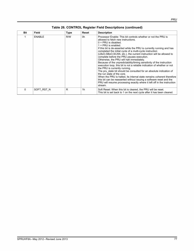
PRU
Table 26. CONTROL Register Field Descriptions (continued)Bit Field Type Reset Description1 ENABLE R/W 0h Processor Enable: This bit controls whether or not the PRU is
allowed to fetch new instructions.0 = PRU is disabled.1 = PRU is enabled.If this bit is de-asserted while the PRU is currently running and hascompleted the initial cycle of a multi-cycle instruction(LBxO,SBxO,SCAN, etc.), the current instruction will be allowed tocomplete before the PRU pauses execution.Otherwise, the PRU will halt immediately.Because of the unpredictability/timing sensitivity of the instructionexecution loop, this bit is not a reliable indication of whether or notthe PRU is currently running.The pru_state bit should be consulted for an absolute indication ofthe run state of the core.When the PRU is halted, its internal state remains coherent thereforethis bit can be reasserted without issuing a software reset and thePRU will resume processing exactly where it left off in the instructionstream.
0 SOFT_RST_N R 1h Soft Reset: When this bit is cleared, the PRU will be reset.This bit is set back to 1 on the next cycle after it has been cleared.
77SPRUHF8A–May 2012–Revised June 2013

PRU
5.4.2 STATUS Register (offset = 4h) [reset = 0h]STATUS is shown in Figure 19 and described in Table 27.
STATUS REGISTER
Figure 19. STATUS Register31 30 29 28 27 26 25 24 23 22 21 20 19 18 17 16 15 14 13 12 11 10 9 8 7 6 5 4 3 2 1 0
Reserved PCOUNTER
R-0h
LEGEND: R/W = Read/Write; R = Read only; W1toCl = Write 1 to clear bit; -n = value after reset
Table 27. STATUS Register Field Descriptions
Bit Field Type Reset Description15-0 PCOUNTER R 0h Program Counter: This field is a registered (1 cycle delayed)
reflection of the PRU program counter.Note that the PC is an instruction address where each instruction isa 32 bit word.This is not a byte address and to compute the byte address justmultiply the PC by 4 (PC of2 = byte address of 0x8, or PC of8 = byte address of 0x20).
78 SPRUHF8A–May 2012–Revised June 2013

PRU
5.4.3 WAKEUP_EN Register (offset = 8h) [reset = 0h]WAKEUP_EN is shown in Figure 20 and described in Table 28.
WAKEUP ENABLE REGISTER
Figure 20. WAKEUP_EN Register31 30 29 28 27 26 25 24 23 22 21 20 19 18 17 16 15 14 13 12 11 10 9 8 7 6 5 4 3 2 1 0
BITWISE_ENABLES
R/W-0h
LEGEND: R/W = Read/Write; R = Read only; W1toCl = Write 1 to clear bit; -n = value after reset
Table 28. WAKEUP_EN Register Field Descriptions
Bit Field Type Reset Description31-0 BITWISE_ENABLES R/W 0h Wakeup Enables: This field is ANDed with the incoming R31 status
inputs (whose bit positions were specified in the stmap parameter) toproduce a vector which is unary ORed to produce thestatus_wakeup source for the core.Setting any bit in this vector will allow the corresponding status inputto wake up the core when it is asserted high.The PRU should set this enable vector prior to executing a SLP(sleep) instruction to ensure that the desired sources can wake upthe core.
79SPRUHF8A–May 2012–Revised June 2013

PRU
5.4.4 CYCLE Register (offset = Ch) [reset = 0h]CYCLE is shown in Figure 21 and described in Table 29.
CYCLE COUNT. This register counts the number of cycles for which the PRU has been enabled.
Figure 21. CYCLE Register31 30 29 28 27 26 25 24 23 22 21 20 19 18 17 16 15 14 13 12 11 10 9 8 7 6 5 4 3 2 1 0
CYCLECOUNT
0h
LEGEND: R/W = Read/Write; R = Read only; W1toCl = Write 1 to clear bit; -n = value after reset
Table 29. CYCLE Register Field Descriptions
Bit Field Type Reset Description31-0 CYCLECOUNT 0h This value is incremented by 1 for every cycle during which the PRU
is enabled and the counter is enabled (both bits ENABLE andCOUNTENABLE set in the PRU control register).Counting halts while the PRU is disabled or counter is disabled, andresumes when re-eneabled.Counter clears the COUNTENABLE bit in the PRU control registerwhen the count reaches 0xFFFFFFFF.(Count does does not wrap).The register can be read at any time.The register can be cleared when the counter or PRU is disabled.Clearing this register also clears the PRU Stall Count Register.
80 SPRUHF8A–May 2012–Revised June 2013

PRU
5.4.5 STALL Register (offset = 10h) [reset = 0h]STALL is shown in Figure 22 and described in Table 30.
STALL COUNT. This register counts the number of cycles for which the PRU has been enabled, butunable to fetch a new instruction. It is linked to the Cycle Count Register (0x0C) such that this registerreflects the stall cycles measured over the same cycles as counted by the cycle count register. Thus thevalue of this register is always less than or equal to cycle count.
Figure 22. STALL Register31 30 29 28 27 26 25 24 23 22 21 20 19 18 17 16 15 14 13 12 11 10 9 8 7 6 5 4 3 2 1 0
STALLCOUNT
0h
LEGEND: R/W = Read/Write; R = Read only; W1toCl = Write 1 to clear bit; -n = value after reset
Table 30. STALL Register Field Descriptions
Bit Field Type Reset Description31-0 STALLCOUNT 0h This value is incremented by 1 for every cycle during which the PRU
is enabled and the counter is enabled (both bits ENABLE andCOUNTENABLE set in the PRU control register), and the PRU wasunable to fetch a new instruction for any reason.
81SPRUHF8A–May 2012–Revised June 2013

PRU
5.4.6 CTBIR0 Register (offset = 20h) [reset = 0h]CTBIR0 is shown in Figure 23 and described in Table 31.
CONSTANT TABLE BLOCK INDEX REGISTER 0. This register is used to set the block indices which areused to modify entries 24 and 25 in the PRU Constant Table. This register can be written by the PRUwhenever it needs to change to a new base pointer for a block in the State / Scratchpad RAM. Thisfunction is useful since the PRU is often processing multiple processing threads which require it to changecontexts. The PRU can use this register to avoid requiring excessive amounts of code for repetitivecontext switching. The format of this register is as follows:
Figure 23. CTBIR0 Register31 30 29 28 27 26 25 24
Reserved
23 22 21 20 19 18 17 16
C25_BLK_INDEX
R/W-0h
15 14 13 12 11 10 9 8
Reserved
7 6 5 4 3 2 1 0
C24_BLK_INDEX
R/W-0h
LEGEND: R/W = Read/Write; R = Read only; W1toCl = Write 1 to clear bit; -n = value after reset
Table 31. CTBIR0 Register Field Descriptions
Bit Field Type Reset Description23-16 C25_BLK_INDEX R/W 0h PRU Constant Entry 25 Block Index: This field sets the value that will
appear in bits11:8 of entry 25 in the PRU Constant Table.
7-0 C24_BLK_INDEX R/W 0h PRU Constant Entry 24 Block Index: This field sets the value that willappear in bits11:8 of entry 24 in the PRU Constant Table.
82 SPRUHF8A–May 2012–Revised June 2013

PRU
5.4.7 CTBIR1 Register (offset = 24h) [reset = 0h]CTBIR1 is shown in Figure 24 and described in Table 32.
CONSTANT TABLE BLOCK INDEX REGISTER 1. This register is used to set the block indices which areused to modify entries 24 and 25 in the PRU Constant Table. This register can be written by the PRUwhenever it needs to change to a new base pointer for a block in the State / Scratchpad RAM. Thisfunction is useful since the PRU is often processing multiple processing threads which require it to changecontexts. The PRU can use this register to avoid requiring excessive amounts of code for repetitivecontext switching. The format of this register is as follows:
Figure 24. CTBIR1 Register31 30 29 28 27 26 25 24
Reserved
23 22 21 20 19 18 17 16
C27_BLK_INDEX
R/W-0h
15 14 13 12 11 10 9 8
Reserved
7 6 5 4 3 2 1 0
C26_BLK_INDEX
R/W-0h
LEGEND: R/W = Read/Write; R = Read only; W1toCl = Write 1 to clear bit; -n = value after reset
Table 32. CTBIR1 Register Field Descriptions
Bit Field Type Reset Description23-16 C27_BLK_INDEX R/W 0h PRU Constant Entry 27 Block Index: This field sets the value that will
appear in bits11:8 of entry 27 in the PRU Constant Table.
7-0 C26_BLK_INDEX R/W 0h PRU Constant Entry 26 Block Index: This field sets the value that willappear in bits11:8 of entry 26 in the PRU Constant Table.
83SPRUHF8A–May 2012–Revised June 2013

PRU
5.4.8 CTPPR0 Register (offset = 28h) [reset = 0h]CTPPR0 is shown in Figure 25 and described in Table 33.
CONSTANT TABLE PROGRAMMABLE POINTER REGISTER 0. This register allows the PRU to set upthe 256-byte page index for entries 28 and 29 in the PRU Constant Table which serve as general purposepointers which can be configured to point to any locations inside the session router address map. Thisregister is useful when the PRU needs to frequently access certain structures inside the session routeraddress space whose locations are not hard coded such as tables in scratchpad memory. This register isformatted as follows:
Figure 25. CTPPR0 Register31 30 29 28 27 26 25 24
C29_POINTER
R/W-0h
23 22 21 20 19 18 17 16
C29_POINTER
R/W-0h
15 14 13 12 11 10 9 8
C28_POINTER
R/W-0h
7 6 5 4 3 2 1 0
C28_POINTER
R/W-0h
LEGEND: R/W = Read/Write; R = Read only; W1toCl = Write 1 to clear bit; -n = value after reset
Table 33. CTPPR0 Register Field Descriptions
Bit Field Type Reset Description31-16 C29_POINTER R/W 0h PRU Constant Entry 29 Pointer: This field sets the value that will
appear in bits23:8 of entry 29 in the PRU Constant Table.
15-0 C28_POINTER R/W 0h PRU Constant Entry 28 Pointer: This field sets the value that willappear in bits23:8 of entry 28 in the PRU Constant Table.
84 SPRUHF8A–May 2012–Revised June 2013

PRU
5.4.9 CTPPR1 Register (offset = 2Ch) [reset = 0h]CTPPR1 is shown in Figure 26 and described in Table 34.
CONSTANT TABLE PROGRAMMABLE POINTER REGISTER 1. This register functions the same as thePRU Constant Table Programmable Pointer Register 0 but allows the PRU to control entries 30 and 31 inthe PRU Constant Table. This register is formatted as follows:
Figure 26. CTPPR1 Register31 30 29 28 27 26 25 24
C31_POINTER
R/W-0h
23 22 21 20 19 18 17 16
C31_POINTER
R/W-0h
15 14 13 12 11 10 9 8
C30_POINTER
R/W-0h
7 6 5 4 3 2 1 0
C30_POINTER
R/W-0h
LEGEND: R/W = Read/Write; R = Read only; W1toCl = Write 1 to clear bit; -n = value after reset
Table 34. CTPPR1 Register Field Descriptions
Bit Field Type Reset Description31-16 C31_POINTER R/W 0h PRU Constant Entry 31 Pointer: This field sets the value that will
appear in bits23:8 of entry 31 in the PRU Constant Table.
15-0 C30_POINTER R/W 0h PRU Constant Entry 30 Pointer: This field sets the value that willappear in bits23:8 of entry 30 in the PRU Constant Table.
5.5 PRU_ICSS_PRU_DEBUG Registers
Table 35 lists the memory-mapped registers for the PRU_ICSS_PRU_DEBUG. All register offsetaddresses not listed in Table 35 should be considered as reserved locations and the register contentsshould not be modified.
Table 35. PRU_ICSS_PRU_DEBUG REGISTERSOffset Acronym Register Name Section
0h GPREG0 Section 5.5.14h GPREG1 Section 5.5.28h GPREG2 Section 5.5.3Ch GPREG3 Section 5.5.410h GPREG4 Section 5.5.514h GPREG5 Section 5.5.618h GPREG6 Section 5.5.71Ch GPREG7 Section 5.5.820h GPREG8 Section 5.5.924h GPREG9 Section 5.5.1028h GPREG10 Section 5.5.112Ch GPREG11 Section 5.5.1230h GPREG12 Section 5.5.1334h GPREG13 Section 5.5.14
85SPRUHF8A–May 2012–Revised June 2013

PRU
Table 35. PRU_ICSS_PRU_DEBUG REGISTERS (continued)Offset Acronym Register Name Section
38h GPREG14 Section 5.5.153Ch GPREG15 Section 5.5.1640h GPREG16 Section 5.5.1744h GPREG17 Section 5.5.1848h GPREG18 Section 5.5.194Ch GPREG19 Section 5.5.2050h GPREG20 Section 5.5.2154h GPREG21 Section 5.5.2258h GPREG22 Section 5.5.235Ch GPREG23 Section 5.5.2460h GPREG24 Section 5.5.2564h GPREG25 Section 5.5.2668h GPREG26 Section 5.5.276Ch GPREG27 Section 5.5.2870h GPREG28 Section 5.5.2974h GPREG29 Section 5.5.3078h GPREG30 Section 5.5.317Ch GPREG31 Section 5.5.3280h CT_REG0 Section 5.5.3384h CT_REG1 Section 5.5.3488h CT_REG2 Section 5.5.358Ch CT_REG3 Section 5.5.3690h CT_REG4 Section 5.5.3794h CT_REG5 Section 5.5.3898h CT_REG6 Section 5.5.399Ch CT_REG7 Section 5.5.40A0h CT_REG8 Section 5.5.41A4h CT_REG9 Section 5.5.42A8h CT_REG10 Section 5.5.43ACh CT_REG11 Section 5.5.44B0h CT_REG12 Section 5.5.45B4h CT_REG13 Section 5.5.46B8h CT_REG14 Section 5.5.47BCh CT_REG15 Section 5.5.48C0h CT_REG16 Section 5.5.49C4h CT_REG17 Section 5.5.50C8h CT_REG18 Section 5.5.51CCh CT_REG19 Section 5.5.52D0h CT_REG20 Section 5.5.53D4h CT_REG21 Section 5.5.54D8h CT_REG22 Section 5.5.55DCh CT_REG23 Section 5.5.56E0h CT_REG24 Section 5.5.57E4h CT_REG25 Section 5.5.58E8h CT_REG26 Section 5.5.59ECh CT_REG27 Section 5.5.60F0h CT_REG28 Section 5.5.61
86 SPRUHF8A–May 2012–Revised June 2013

PRU
Table 35. PRU_ICSS_PRU_DEBUG REGISTERS (continued)Offset Acronym Register Name Section
F4h CT_REG29 Section 5.5.62F8h CT_REG30 Section 5.5.63FCh CT_REG31 Section 5.5.64
87SPRUHF8A–May 2012–Revised June 2013

PRU
5.5.1 GPREG0 Register (offset = 0h) [reset = 0h]GPREG0 is shown in Figure 27 and described in Table 36.
DEBUG PRU GENERAL PURPOSE REGISTER 0. This register allows an external agent to debug thePRU while it is disabled. Reading or writing to these registers will have the same effect as a read or writeto these registers from an internal instruction in the PRU. For R30, this includes generation of the pulseoutputs whenever the register is written.
Figure 27. GPREG0 Register31 30 29 28 27 26 25 24 23 22 21 20 19 18 17 16 15 14 13 12 11 10 9 8 7 6 5 4 3 2 1 0
GP_REGISTER0
R/W-0h
LEGEND: R/W = Read/Write; R = Read only; W1toCl = Write 1 to clear bit; -n = value after reset
Table 36. GPREG0 Register Field Descriptions
Bit Field Type Reset Description31-0 GP_REGISTER0 R/W 0h PRU Internal GP Register n: Reading / writing this field directly
inspects/modifies the corresponding internal register in the PRUinternal regfile.
88 SPRUHF8A–May 2012–Revised June 2013

PRU
5.5.2 GPREG1 Register (offset = 4h) [reset = 0h]GPREG1 is shown in Figure 28 and described in Table 37.
DEBUG PRU GENERAL PURPOSE REGISTER 1. This register allows an external agent to debug thePRU while it is disabled. Reading or writing to these registers will have the same effect as a read or writeto these registers from an internal instruction in the PRU. For R30, this includes generation of the pulseoutputs whenever the register is written.
Figure 28. GPREG1 Register31 30 29 28 27 26 25 24 23 22 21 20 19 18 17 16 15 14 13 12 11 10 9 8 7 6 5 4 3 2 1 0
GP_REGISTER1
R/W-0h
LEGEND: R/W = Read/Write; R = Read only; W1toCl = Write 1 to clear bit; -n = value after reset
Table 37. GPREG1 Register Field Descriptions
Bit Field Type Reset Description31-0 GP_REGISTER1 R/W 0h PRU Internal GP Register n: Reading / writing this field directly
inspects/modifies the corresponding internal register in the PRUinternal regfile.
89SPRUHF8A–May 2012–Revised June 2013

PRU
5.5.3 GPREG2 Register (offset = 8h) [reset = 0h]GPREG2 is shown in Figure 29 and described in Table 38.
DEBUG PRU GENERAL PURPOSE REGISTER 2. This register allows an external agent to debug thePRU while it is disabled. Reading or writing to these registers will have the same effect as a read or writeto these registers from an internal instruction in the PRU. For R30, this includes generation of the pulseoutputs whenever the register is written.
Figure 29. GPREG2 Register31 30 29 28 27 26 25 24 23 22 21 20 19 18 17 16 15 14 13 12 11 10 9 8 7 6 5 4 3 2 1 0
GP_REGISTER2
R/W-0h
LEGEND: R/W = Read/Write; R = Read only; W1toCl = Write 1 to clear bit; -n = value after reset
Table 38. GPREG2 Register Field Descriptions
Bit Field Type Reset Description31-0 GP_REGISTER2 R/W 0h PRU Internal GP Register n: Reading / writing this field directly
inspects/modifies the corresponding internal register in the PRUinternal regfile.
90 SPRUHF8A–May 2012–Revised June 2013

PRU
5.5.4 GPREG3 Register (offset = Ch) [reset = 0h]GPREG3 is shown in Figure 30 and described in Table 39.
DEBUG PRU GENERAL PURPOSE REGISTER 3. This register allows an external agent to debug thePRU while it is disabled. Reading or writing to these registers will have the same effect as a read or writeto these registers from an internal instruction in the PRU. For R30, this includes generation of the pulseoutputs whenever the register is written.
Figure 30. GPREG3 Register31 30 29 28 27 26 25 24 23 22 21 20 19 18 17 16 15 14 13 12 11 10 9 8 7 6 5 4 3 2 1 0
GP_REGISTER3
R/W-0h
LEGEND: R/W = Read/Write; R = Read only; W1toCl = Write 1 to clear bit; -n = value after reset
Table 39. GPREG3 Register Field Descriptions
Bit Field Type Reset Description31-0 GP_REGISTER3 R/W 0h PRU Internal GP Register n: Reading / writing this field directly
inspects/modifies the corresponding internal register in the PRUinternal regfile.
91SPRUHF8A–May 2012–Revised June 2013

PRU
5.5.5 GPREG4 Register (offset = 10h) [reset = 0h]GPREG4 is shown in Figure 31 and described in Table 40.
DEBUG PRU GENERAL PURPOSE REGISTER 4. This register allows an external agent to debug thePRU while it is disabled. Reading or writing to these registers will have the same effect as a read or writeto these registers from an internal instruction in the PRU. For R30, this includes generation of the pulseoutputs whenever the register is written.
Figure 31. GPREG4 Register31 30 29 28 27 26 25 24 23 22 21 20 19 18 17 16 15 14 13 12 11 10 9 8 7 6 5 4 3 2 1 0
GP_REGISTER4
R/W-0h
LEGEND: R/W = Read/Write; R = Read only; W1toCl = Write 1 to clear bit; -n = value after reset
Table 40. GPREG4 Register Field Descriptions
Bit Field Type Reset Description31-0 GP_REGISTER4 R/W 0h PRU Internal GP Register n: Reading / writing this field directly
inspects/modifies the corresponding internal register in the PRUinternal regfile.
92 SPRUHF8A–May 2012–Revised June 2013

PRU
5.5.6 GPREG5 Register (offset = 14h) [reset = 0h]GPREG5 is shown in Figure 32 and described in Table 41.
DEBUG PRU GENERAL PURPOSE REGISTER 5. This register allows an external agent to debug thePRU while it is disabled. Reading or writing to these registers will have the same effect as a read or writeto these registers from an internal instruction in the PRU. For R30, this includes generation of the pulseoutputs whenever the register is written.
Figure 32. GPREG5 Register31 30 29 28 27 26 25 24 23 22 21 20 19 18 17 16 15 14 13 12 11 10 9 8 7 6 5 4 3 2 1 0
GP_REGISTER5
R/W-0h
LEGEND: R/W = Read/Write; R = Read only; W1toCl = Write 1 to clear bit; -n = value after reset
Table 41. GPREG5 Register Field Descriptions
Bit Field Type Reset Description31-0 GP_REGISTER5 R/W 0h PRU Internal GP Register n: Reading / writing this field directly
inspects/modifies the corresponding internal register in the PRUinternal regfile.
93SPRUHF8A–May 2012–Revised June 2013

PRU
5.5.7 GPREG6 Register (offset = 18h) [reset = 0h]GPREG6 is shown in Figure 33 and described in Table 42.
DEBUG PRU GENERAL PURPOSE REGISTER 6. This register allows an external agent to debug thePRU while it is disabled. Reading or writing to these registers will have the same effect as a read or writeto these registers from an internal instruction in the PRU. For R30, this includes generation of the pulseoutputs whenever the register is written.
Figure 33. GPREG6 Register31 30 29 28 27 26 25 24 23 22 21 20 19 18 17 16 15 14 13 12 11 10 9 8 7 6 5 4 3 2 1 0
GP_REGISTER6
R/W-0h
LEGEND: R/W = Read/Write; R = Read only; W1toCl = Write 1 to clear bit; -n = value after reset
Table 42. GPREG6 Register Field Descriptions
Bit Field Type Reset Description31-0 GP_REGISTER6 R/W 0h PRU Internal GP Register n: Reading / writing this field directly
inspects/modifies the corresponding internal register in the PRUinternal regfile.
94 SPRUHF8A–May 2012–Revised June 2013

PRU
5.5.8 GPREG7 Register (offset = 1Ch) [reset = 0h]GPREG7 is shown in Figure 34 and described in Table 43.
DEBUG PRU GENERAL PURPOSE REGISTER 7. This register allows an external agent to debug thePRU while it is disabled. Reading or writing to these registers will have the same effect as a read or writeto these registers from an internal instruction in the PRU. For R30, this includes generation of the pulseoutputs whenever the register is written.
Figure 34. GPREG7 Register31 30 29 28 27 26 25 24 23 22 21 20 19 18 17 16 15 14 13 12 11 10 9 8 7 6 5 4 3 2 1 0
GP_REGISTER7
R/W-0h
LEGEND: R/W = Read/Write; R = Read only; W1toCl = Write 1 to clear bit; -n = value after reset
Table 43. GPREG7 Register Field Descriptions
Bit Field Type Reset Description31-0 GP_REGISTER7 R/W 0h PRU Internal GP Register n: Reading / writing this field directly
inspects/modifies the corresponding internal register in the PRUinternal regfile.
95SPRUHF8A–May 2012–Revised June 2013

PRU
5.5.9 GPREG8 Register (offset = 20h) [reset = 0h]GPREG8 is shown in Figure 35 and described in Table 44.
DEBUG PRU GENERAL PURPOSE REGISTER 8. This register allows an external agent to debug thePRU while it is disabled. Reading or writing to these registers will have the same effect as a read or writeto these registers from an internal instruction in the PRU. For R30, this includes generation of the pulseoutputs whenever the register is written.
Figure 35. GPREG8 Register31 30 29 28 27 26 25 24 23 22 21 20 19 18 17 16 15 14 13 12 11 10 9 8 7 6 5 4 3 2 1 0
GP_REGISTER8
R/W-0h
LEGEND: R/W = Read/Write; R = Read only; W1toCl = Write 1 to clear bit; -n = value after reset
Table 44. GPREG8 Register Field Descriptions
Bit Field Type Reset Description31-0 GP_REGISTER8 R/W 0h PRU Internal GP Register n: Reading / writing this field directly
inspects/modifies the corresponding internal register in the PRUinternal regfile.
96 SPRUHF8A–May 2012–Revised June 2013

PRU
5.5.10 GPREG9 Register (offset = 24h) [reset = 0h]GPREG9 is shown in Figure 36 and described in Table 45.
DEBUG PRU GENERAL PURPOSE REGISTER 9. This register allows an external agent to debug thePRU while it is disabled. Reading or writing to these registers will have the same effect as a read or writeto these registers from an internal instruction in the PRU. For R30, this includes generation of the pulseoutputs whenever the register is written.
Figure 36. GPREG9 Register31 30 29 28 27 26 25 24 23 22 21 20 19 18 17 16 15 14 13 12 11 10 9 8 7 6 5 4 3 2 1 0
GP_REGISTER9
R/W-0h
LEGEND: R/W = Read/Write; R = Read only; W1toCl = Write 1 to clear bit; -n = value after reset
Table 45. GPREG9 Register Field Descriptions
Bit Field Type Reset Description31-0 GP_REGISTER9 R/W 0h PRU Internal GP Register n: Reading / writing this field directly
inspects/modifies the corresponding internal register in the PRUinternal regfile.
97SPRUHF8A–May 2012–Revised June 2013

PRU
5.5.11 GPREG10 Register (offset = 28h) [reset = 0h]GPREG10 is shown in Figure 37 and described in Table 46.
DEBUG PRU GENERAL PURPOSE REGISTER 10. This register allows an external agent to debug thePRU while it is disabled. Reading or writing to these registers will have the same effect as a read or writeto these registers from an internal instruction in the PRU. For R30, this includes generation of the pulseoutputs whenever the register is written.
Figure 37. GPREG10 Register31 30 29 28 27 26 25 24 23 22 21 20 19 18 17 16 15 14 13 12 11 10 9 8 7 6 5 4 3 2 1 0
GP_REGISTER10
R/W-0h
LEGEND: R/W = Read/Write; R = Read only; W1toCl = Write 1 to clear bit; -n = value after reset
Table 46. GPREG10 Register Field Descriptions
Bit Field Type Reset Description31-0 GP_REGISTER10 R/W 0h PRU Internal GP Register n: Reading / writing this field directly
inspects/modifies the corresponding internal register in the PRUinternal regfile.
98 SPRUHF8A–May 2012–Revised June 2013

PRU
5.5.12 GPREG11 Register (offset = 2Ch) [reset = 0h]GPREG11 is shown in Figure 38 and described in Table 47.
DEBUG PRU GENERAL PURPOSE REGISTER 11. This register allows an external agent to debug thePRU while it is disabled. Reading or writing to these registers will have the same effect as a read or writeto these registers from an internal instruction in the PRU. For R30, this includes generation of the pulseoutputs whenever the register is written.
Figure 38. GPREG11 Register31 30 29 28 27 26 25 24 23 22 21 20 19 18 17 16 15 14 13 12 11 10 9 8 7 6 5 4 3 2 1 0
GP_REGISTER11
R/W-0h
LEGEND: R/W = Read/Write; R = Read only; W1toCl = Write 1 to clear bit; -n = value after reset
Table 47. GPREG11 Register Field Descriptions
Bit Field Type Reset Description31-0 GP_REGISTER11 R/W 0h PRU Internal GP Register n: Reading / writing this field directly
inspects/modifies the corresponding internal register in the PRUinternal regfile.
99SPRUHF8A–May 2012–Revised June 2013

PRU
5.5.13 GPREG12 Register (offset = 30h) [reset = 0h]GPREG12 is shown in Figure 39 and described in Table 48.
DEBUG PRU GENERAL PURPOSE REGISTER 12. This register allows an external agent to debug thePRU while it is disabled. Reading or writing to these registers will have the same effect as a read or writeto these registers from an internal instruction in the PRU. For R30, this includes generation of the pulseoutputs whenever the register is written.
Figure 39. GPREG12 Register31 30 29 28 27 26 25 24 23 22 21 20 19 18 17 16 15 14 13 12 11 10 9 8 7 6 5 4 3 2 1 0
GP_REGISTER12
R/W-0h
LEGEND: R/W = Read/Write; R = Read only; W1toCl = Write 1 to clear bit; -n = value after reset
Table 48. GPREG12 Register Field Descriptions
Bit Field Type Reset Description31-0 GP_REGISTER12 R/W 0h PRU Internal GP Register n: Reading / writing this field directly
inspects/modifies the corresponding internal register in the PRUinternal regfile.
100 SPRUHF8A–May 2012–Revised June 2013

PRU
5.5.14 GPREG13 Register (offset = 34h) [reset = 0h]GPREG13 is shown in Figure 40 and described in Table 49.
DEBUG PRU GENERAL PURPOSE REGISTER 13. This register allows an external agent to debug thePRU while it is disabled. Reading or writing to these registers will have the same effect as a read or writeto these registers from an internal instruction in the PRU. For R30, this includes generation of the pulseoutputs whenever the register is written.
Figure 40. GPREG13 Register31 30 29 28 27 26 25 24 23 22 21 20 19 18 17 16 15 14 13 12 11 10 9 8 7 6 5 4 3 2 1 0
GP_REGISTER13
R/W-0h
LEGEND: R/W = Read/Write; R = Read only; W1toCl = Write 1 to clear bit; -n = value after reset
Table 49. GPREG13 Register Field Descriptions
Bit Field Type Reset Description31-0 GP_REGISTER13 R/W 0h PRU Internal GP Register n: Reading / writing this field directly
inspects/modifies the corresponding internal register in the PRUinternal regfile.
101SPRUHF8A–May 2012–Revised June 2013

PRU
5.5.15 GPREG14 Register (offset = 38h) [reset = 0h]GPREG14 is shown in Figure 41 and described in Table 50.
DEBUG PRU GENERAL PURPOSE REGISTER 14. This register allows an external agent to debug thePRU while it is disabled. Reading or writing to these registers will have the same effect as a read or writeto these registers from an internal instruction in the PRU. For R30, this includes generation of the pulseoutputs whenever the register is written.
Figure 41. GPREG14 Register31 30 29 28 27 26 25 24 23 22 21 20 19 18 17 16 15 14 13 12 11 10 9 8 7 6 5 4 3 2 1 0
GP_REGISTER14
R/W-0h
LEGEND: R/W = Read/Write; R = Read only; W1toCl = Write 1 to clear bit; -n = value after reset
Table 50. GPREG14 Register Field Descriptions
Bit Field Type Reset Description31-0 GP_REGISTER14 R/W 0h PRU Internal GP Register n: Reading / writing this field directly
inspects/modifies the corresponding internal register in the PRUinternal regfile.
102 SPRUHF8A–May 2012–Revised June 2013

PRU
5.5.16 GPREG15 Register (offset = 3Ch) [reset = 0h]GPREG15 is shown in Figure 42 and described in Table 51.
DEBUG PRU GENERAL PURPOSE REGISTER 15. This register allows an external agent to debug thePRU while it is disabled. Reading or writing to these registers will have the same effect as a read or writeto these registers from an internal instruction in the PRU. For R30, this includes generation of the pulseoutputs whenever the register is written.
Figure 42. GPREG15 Register31 30 29 28 27 26 25 24 23 22 21 20 19 18 17 16 15 14 13 12 11 10 9 8 7 6 5 4 3 2 1 0
GP_REGISTER15
R/W-0h
LEGEND: R/W = Read/Write; R = Read only; W1toCl = Write 1 to clear bit; -n = value after reset
Table 51. GPREG15 Register Field Descriptions
Bit Field Type Reset Description31-0 GP_REGISTER15 R/W 0h PRU Internal GP Register n: Reading / writing this field directly
inspects/modifies the corresponding internal register in the PRUinternal regfile.
103SPRUHF8A–May 2012–Revised June 2013

PRU
5.5.17 GPREG16 Register (offset = 40h) [reset = 0h]GPREG16 is shown in Figure 43 and described in Table 52.
DEBUG PRU GENERAL PURPOSE REGISTER 16. This register allows an external agent to debug thePRU while it is disabled. Reading or writing to these registers will have the same effect as a read or writeto these registers from an internal instruction in the PRU. For R30, this includes generation of the pulseoutputs whenever the register is written.
Figure 43. GPREG16 Register31 30 29 28 27 26 25 24 23 22 21 20 19 18 17 16 15 14 13 12 11 10 9 8 7 6 5 4 3 2 1 0
GP_REGISTER16
R/W-0h
LEGEND: R/W = Read/Write; R = Read only; W1toCl = Write 1 to clear bit; -n = value after reset
Table 52. GPREG16 Register Field Descriptions
Bit Field Type Reset Description31-0 GP_REGISTER16 R/W 0h PRU Internal GP Register n: Reading / writing this field directly
inspects/modifies the corresponding internal register in the PRUinternal regfile.
104 SPRUHF8A–May 2012–Revised June 2013

PRU
5.5.18 GPREG17 Register (offset = 44h) [reset = 0h]GPREG17 is shown in Figure 44 and described in Table 53.
DEBUG PRU GENERAL PURPOSE REGISTER 17. This register allows an external agent to debug thePRU while it is disabled. Reading or writing to these registers will have the same effect as a read or writeto these registers from an internal instruction in the PRU. For R30, this includes generation of the pulseoutputs whenever the register is written.
Figure 44. GPREG17 Register31 30 29 28 27 26 25 24 23 22 21 20 19 18 17 16 15 14 13 12 11 10 9 8 7 6 5 4 3 2 1 0
GP_REGISTER17
R/W-0h
LEGEND: R/W = Read/Write; R = Read only; W1toCl = Write 1 to clear bit; -n = value after reset
Table 53. GPREG17 Register Field Descriptions
Bit Field Type Reset Description31-0 GP_REGISTER17 R/W 0h PRU Internal GP Register n: Reading / writing this field directly
inspects/modifies the corresponding internal register in the PRUinternal regfile.
105SPRUHF8A–May 2012–Revised June 2013
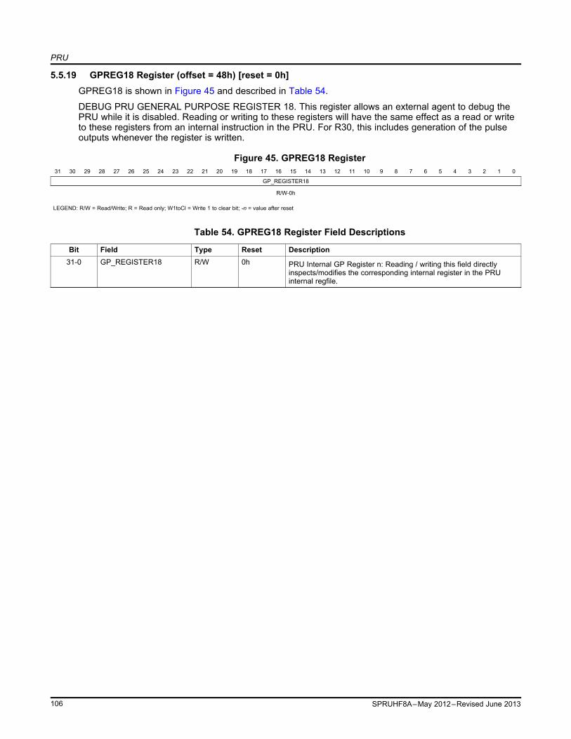
PRU
5.5.19 GPREG18 Register (offset = 48h) [reset = 0h]GPREG18 is shown in Figure 45 and described in Table 54.
DEBUG PRU GENERAL PURPOSE REGISTER 18. This register allows an external agent to debug thePRU while it is disabled. Reading or writing to these registers will have the same effect as a read or writeto these registers from an internal instruction in the PRU. For R30, this includes generation of the pulseoutputs whenever the register is written.
Figure 45. GPREG18 Register31 30 29 28 27 26 25 24 23 22 21 20 19 18 17 16 15 14 13 12 11 10 9 8 7 6 5 4 3 2 1 0
GP_REGISTER18
R/W-0h
LEGEND: R/W = Read/Write; R = Read only; W1toCl = Write 1 to clear bit; -n = value after reset
Table 54. GPREG18 Register Field Descriptions
Bit Field Type Reset Description31-0 GP_REGISTER18 R/W 0h PRU Internal GP Register n: Reading / writing this field directly
inspects/modifies the corresponding internal register in the PRUinternal regfile.
106 SPRUHF8A–May 2012–Revised June 2013

PRU
5.5.20 GPREG19 Register (offset = 4Ch) [reset = 0h]GPREG19 is shown in Figure 46 and described in Table 55.
DEBUG PRU GENERAL PURPOSE REGISTER 19. This register allows an external agent to debug thePRU while it is disabled. Reading or writing to these registers will have the same effect as a read or writeto these registers from an internal instruction in the PRU. For R30, this includes generation of the pulseoutputs whenever the register is written.
Figure 46. GPREG19 Register31 30 29 28 27 26 25 24 23 22 21 20 19 18 17 16 15 14 13 12 11 10 9 8 7 6 5 4 3 2 1 0
GP_REGISTER19
R/W-0h
LEGEND: R/W = Read/Write; R = Read only; W1toCl = Write 1 to clear bit; -n = value after reset
Table 55. GPREG19 Register Field Descriptions
Bit Field Type Reset Description31-0 GP_REGISTER19 R/W 0h PRU Internal GP Register n: Reading / writing this field directly
inspects/modifies the corresponding internal register in the PRUinternal regfile.
107SPRUHF8A–May 2012–Revised June 2013

PRU
5.5.21 GPREG20 Register (offset = 50h) [reset = 0h]GPREG20 is shown in Figure 47 and described in Table 56.
DEBUG PRU GENERAL PURPOSE REGISTER 20. This register allows an external agent to debug thePRU while it is disabled. Reading or writing to these registers will have the same effect as a read or writeto these registers from an internal instruction in the PRU. For R30, this includes generation of the pulseoutputs whenever the register is written.
Figure 47. GPREG20 Register31 30 29 28 27 26 25 24 23 22 21 20 19 18 17 16 15 14 13 12 11 10 9 8 7 6 5 4 3 2 1 0
GP_REGISTER20
R/W-0h
LEGEND: R/W = Read/Write; R = Read only; W1toCl = Write 1 to clear bit; -n = value after reset
Table 56. GPREG20 Register Field Descriptions
Bit Field Type Reset Description31-0 GP_REGISTER20 R/W 0h PRU Internal GP Register n: Reading / writing this field directly
inspects/modifies the corresponding internal register in the PRUinternal regfile.
108 SPRUHF8A–May 2012–Revised June 2013

PRU
5.5.22 GPREG21 Register (offset = 54h) [reset = 0h]GPREG21 is shown in Figure 48 and described in Table 57.
DEBUG PRU GENERAL PURPOSE REGISTER 21. This register allows an external agent to debug thePRU while it is disabled. Reading or writing to these registers will have the same effect as a read or writeto these registers from an internal instruction in the PRU. For R30, this includes generation of the pulseoutputs whenever the register is written.
Figure 48. GPREG21 Register31 30 29 28 27 26 25 24 23 22 21 20 19 18 17 16 15 14 13 12 11 10 9 8 7 6 5 4 3 2 1 0
GP_REGISTER21
R/W-0h
LEGEND: R/W = Read/Write; R = Read only; W1toCl = Write 1 to clear bit; -n = value after reset
Table 57. GPREG21 Register Field Descriptions
Bit Field Type Reset Description31-0 GP_REGISTER21 R/W 0h PRU Internal GP Register n: Reading / writing this field directly
inspects/modifies the corresponding internal register in the PRUinternal regfile.
109SPRUHF8A–May 2012–Revised June 2013

PRU
5.5.23 GPREG22 Register (offset = 58h) [reset = 0h]GPREG22 is shown in Figure 49 and described in Table 58.
DEBUG PRU GENERAL PURPOSE REGISTER 22. This register allows an external agent to debug thePRU while it is disabled. Reading or writing to these registers will have the same effect as a read or writeto these registers from an internal instruction in the PRU. For R30, this includes generation of the pulseoutputs whenever the register is written.
Figure 49. GPREG22 Register31 30 29 28 27 26 25 24 23 22 21 20 19 18 17 16 15 14 13 12 11 10 9 8 7 6 5 4 3 2 1 0
GP_REGISTER22
R/W-0h
LEGEND: R/W = Read/Write; R = Read only; W1toCl = Write 1 to clear bit; -n = value after reset
Table 58. GPREG22 Register Field Descriptions
Bit Field Type Reset Description31-0 GP_REGISTER22 R/W 0h PRU Internal GP Register n: Reading / writing this field directly
inspects/modifies the corresponding internal register in the PRUinternal regfile.
110 SPRUHF8A–May 2012–Revised June 2013

PRU
5.5.24 GPREG23 Register (offset = 5Ch) [reset = 0h]GPREG23 is shown in Figure 50 and described in Table 59.
DEBUG PRU GENERAL PURPOSE REGISTER 23. This register allows an external agent to debug thePRU while it is disabled. Reading or writing to these registers will have the same effect as a read or writeto these registers from an internal instruction in the PRU. For R30, this includes generation of the pulseoutputs whenever the register is written.
Figure 50. GPREG23 Register31 30 29 28 27 26 25 24 23 22 21 20 19 18 17 16 15 14 13 12 11 10 9 8 7 6 5 4 3 2 1 0
GP_REGISTER23
R/W-0h
LEGEND: R/W = Read/Write; R = Read only; W1toCl = Write 1 to clear bit; -n = value after reset
Table 59. GPREG23 Register Field Descriptions
Bit Field Type Reset Description31-0 GP_REGISTER23 R/W 0h PRU Internal GP Register n: Reading / writing this field directly
inspects/modifies the corresponding internal register in the PRUinternal regfile.
111SPRUHF8A–May 2012–Revised June 2013

PRU
5.5.25 GPREG24 Register (offset = 60h) [reset = 0h]GPREG24 is shown in Figure 51 and described in Table 60.
DEBUG PRU GENERAL PURPOSE REGISTER 24. This register allows an external agent to debug thePRU while it is disabled. Reading or writing to these registers will have the same effect as a read or writeto these registers from an internal instruction in the PRU. For R30, this includes generation of the pulseoutputs whenever the register is written.
Figure 51. GPREG24 Register31 30 29 28 27 26 25 24 23 22 21 20 19 18 17 16 15 14 13 12 11 10 9 8 7 6 5 4 3 2 1 0
GP_REGISTER24
R/W-0h
LEGEND: R/W = Read/Write; R = Read only; W1toCl = Write 1 to clear bit; -n = value after reset
Table 60. GPREG24 Register Field Descriptions
Bit Field Type Reset Description31-0 GP_REGISTER24 R/W 0h PRU Internal GP Register n: Reading / writing this field directly
inspects/modifies the corresponding internal register in the PRUinternal regfile.
112 SPRUHF8A–May 2012–Revised June 2013

PRU
5.5.26 GPREG25 Register (offset = 64h) [reset = 0h]GPREG25 is shown in Figure 52 and described in Table 61.
DEBUG PRU GENERAL PURPOSE REGISTER 25. This register allows an external agent to debug thePRU while it is disabled. Reading or writing to these registers will have the same effect as a read or writeto these registers from an internal instruction in the PRU. For R30, this includes generation of the pulseoutputs whenever the register is written.
Figure 52. GPREG25 Register31 30 29 28 27 26 25 24 23 22 21 20 19 18 17 16 15 14 13 12 11 10 9 8 7 6 5 4 3 2 1 0
GP_REGISTER25
R/W-0h
LEGEND: R/W = Read/Write; R = Read only; W1toCl = Write 1 to clear bit; -n = value after reset
Table 61. GPREG25 Register Field Descriptions
Bit Field Type Reset Description31-0 GP_REGISTER25 R/W 0h PRU Internal GP Register n: Reading / writing this field directly
inspects/modifies the corresponding internal register in the PRUinternal regfile.
113SPRUHF8A–May 2012–Revised June 2013

PRU
5.5.27 GPREG26 Register (offset = 68h) [reset = 0h]GPREG26 is shown in Figure 53 and described in Table 62.
DEBUG PRU GENERAL PURPOSE REGISTER 26. This register allows an external agent to debug thePRU while it is disabled. Reading or writing to these registers will have the same effect as a read or writeto these registers from an internal instruction in the PRU. For R30, this includes generation of the pulseoutputs whenever the register is written.
Figure 53. GPREG26 Register31 30 29 28 27 26 25 24 23 22 21 20 19 18 17 16 15 14 13 12 11 10 9 8 7 6 5 4 3 2 1 0
GP_REGISTER26
R/W-0h
LEGEND: R/W = Read/Write; R = Read only; W1toCl = Write 1 to clear bit; -n = value after reset
Table 62. GPREG26 Register Field Descriptions
Bit Field Type Reset Description31-0 GP_REGISTER26 R/W 0h PRU Internal GP Register n: Reading / writing this field directly
inspects/modifies the corresponding internal register in the PRUinternal regfile.
114 SPRUHF8A–May 2012–Revised June 2013

PRU
5.5.28 GPREG27 Register (offset = 6Ch) [reset = 0h]GPREG27 is shown in Figure 54 and described in Table 63.
DEBUG PRU GENERAL PURPOSE REGISTER 27. This register allows an external agent to debug thePRU while it is disabled. Reading or writing to these registers will have the same effect as a read or writeto these registers from an internal instruction in the PRU. For R30, this includes generation of the pulseoutputs whenever the register is written.
Figure 54. GPREG27 Register31 30 29 28 27 26 25 24 23 22 21 20 19 18 17 16 15 14 13 12 11 10 9 8 7 6 5 4 3 2 1 0
GP_REGISTER27
R/W-0h
LEGEND: R/W = Read/Write; R = Read only; W1toCl = Write 1 to clear bit; -n = value after reset
Table 63. GPREG27 Register Field Descriptions
Bit Field Type Reset Description31-0 GP_REGISTER27 R/W 0h PRU Internal GP Register n: Reading / writing this field directly
inspects/modifies the corresponding internal register in the PRUinternal regfile.
115SPRUHF8A–May 2012–Revised June 2013

PRU
5.5.29 GPREG28 Register (offset = 70h) [reset = 0h]GPREG28 is shown in Figure 55 and described in Table 64.
DEBUG PRU GENERAL PURPOSE REGISTER 28. This register allows an external agent to debug thePRU while it is disabled. Reading or writing to these registers will have the same effect as a read or writeto these registers from an internal instruction in the PRU. For R30, this includes generation of the pulseoutputs whenever the register is written.
Figure 55. GPREG28 Register31 30 29 28 27 26 25 24 23 22 21 20 19 18 17 16 15 14 13 12 11 10 9 8 7 6 5 4 3 2 1 0
GP_REGISTER28
R/W-0h
LEGEND: R/W = Read/Write; R = Read only; W1toCl = Write 1 to clear bit; -n = value after reset
Table 64. GPREG28 Register Field Descriptions
Bit Field Type Reset Description31-0 GP_REGISTER28 R/W 0h PRU Internal GP Register n: Reading / writing this field directly
inspects/modifies the corresponding internal register in the PRUinternal regfile.
116 SPRUHF8A–May 2012–Revised June 2013

PRU
5.5.30 GPREG29 Register (offset = 74h) [reset = 0h]GPREG29 is shown in Figure 56 and described in Table 65.
DEBUG PRU GENERAL PURPOSE REGISTER 29. This register allows an external agent to debug thePRU while it is disabled. Reading or writing to these registers will have the same effect as a read or writeto these registers from an internal instruction in the PRU. For R30, this includes generation of the pulseoutputs whenever the register is written.
Figure 56. GPREG29 Register31 30 29 28 27 26 25 24 23 22 21 20 19 18 17 16 15 14 13 12 11 10 9 8 7 6 5 4 3 2 1 0
GP_REGISTER29
R/W-0h
LEGEND: R/W = Read/Write; R = Read only; W1toCl = Write 1 to clear bit; -n = value after reset
Table 65. GPREG29 Register Field Descriptions
Bit Field Type Reset Description31-0 GP_REGISTER29 R/W 0h PRU Internal GP Register n: Reading / writing this field directly
inspects/modifies the corresponding internal register in the PRUinternal regfile.
117SPRUHF8A–May 2012–Revised June 2013

PRU
5.5.31 GPREG30 Register (offset = 78h) [reset = 0h]GPREG30 is shown in Figure 57 and described in Table 66.
DEBUG PRU GENERAL PURPOSE REGISTER 30. This register allows an external agent to debug thePRU while it is disabled. Reading or writing to these registers will have the same effect as a read or writeto these registers from an internal instruction in the PRU. For R30, this includes generation of the pulseoutputs whenever the register is written.
Figure 57. GPREG30 Register31 30 29 28 27 26 25 24 23 22 21 20 19 18 17 16 15 14 13 12 11 10 9 8 7 6 5 4 3 2 1 0
GP_REGISTER30
R/W-0h
LEGEND: R/W = Read/Write; R = Read only; W1toCl = Write 1 to clear bit; -n = value after reset
Table 66. GPREG30 Register Field Descriptions
Bit Field Type Reset Description31-0 GP_REGISTER30 R/W 0h PRU Internal GP Register n: Reading / writing this field directly
inspects/modifies the corresponding internal register in the PRUinternal regfile.
118 SPRUHF8A–May 2012–Revised June 2013

PRU
5.5.32 GPREG31 Register (offset = 7Ch) [reset = 0h]GPREG31 is shown in Figure 58 and described in Table 67.
DEBUG PRU GENERAL PURPOSE REGISTER 31. This register allows an external agent to debug thePRU while it is disabled. Reading or writing to these registers will have the same effect as a read or writeto these registers from an internal instruction in the PRU. For R30, this includes generation of the pulseoutputs whenever the register is written.
Figure 58. GPREG31 Register31 30 29 28 27 26 25 24 23 22 21 20 19 18 17 16 15 14 13 12 11 10 9 8 7 6 5 4 3 2 1 0
GPREG31
R/W-0h
LEGEND: R/W = Read/Write; R = Read only; W1toCl = Write 1 to clear bit; -n = value after reset
Table 67. GPREG31 Register Field Descriptions
Bit Field Type Reset Description31-0 GPREG31 R/W 0h
119SPRUHF8A–May 2012–Revised June 2013

PRU
5.5.33 CT_REG0 Register (offset = 80h) [reset = 20000h]CT_REG0 is shown in Figure 59 and described in Table 68.
DEBUG PRU CONSTANTS TABLE ENTRY 0. This register allows an external agent to debug the PRUwhile it is disabled. Since some of the constants table entries may actually depend on system inputs / andor the internal state of the PRU, these registers are provided to allow an external agent to easilydetermine the state of the constants table.
Figure 59. CT_REG0 Register31 30 29 28 27 26 25 24 23 22 21 20 19 18 17 16 15 14 13 12 11 10 9 8 7 6 5 4 3 2 1 0
CT_REGISTER0
R-20000h
LEGEND: R/W = Read/Write; R = Read only; W1toCl = Write 1 to clear bit; -n = value after reset
Table 68. CT_REG0 Register Field Descriptions
Bit Field Type Reset Description31-0 CT_REGISTER0 R 20000h PRU Internal Constants Table Entry n: Reading this field directly
inspects the corresponding entry in the PRU internal constants table.
120 SPRUHF8A–May 2012–Revised June 2013

PRU
5.5.34 CT_REG1 Register (offset = 84h) [reset = 48040000h]CT_REG1 is shown in Figure 60 and described in Table 69.
DEBUG PRU CONSTANTS TABLE ENTRY 1. This register allows an external agent to debug the PRUwhile it is disabled. Since some of the constants table entries may actually depend on system inputs / andor the internal state of the PRU, these registers are provided to allow an external agent to easilydetermine the state of the constants table.
Figure 60. CT_REG1 Register31 30 29 28 27 26 25 24 23 22 21 20 19 18 17 16 15 14 13 12 11 10 9 8 7 6 5 4 3 2 1 0
CT_REGISTER1
R-48040000h
LEGEND: R/W = Read/Write; R = Read only; W1toCl = Write 1 to clear bit; -n = value after reset
Table 69. CT_REG1 Register Field Descriptions
Bit Field Type Reset Description31-0 CT_REGISTER1 R 48040000h PRU Internal Constants Table Entry n: Reading this field directly
inspects the corresponding entry in the PRU internal constants table.
121SPRUHF8A–May 2012–Revised June 2013

PRU
5.5.35 CT_REG2 Register (offset = 88h) [reset = 4802A000h]CT_REG2 is shown in Figure 61 and described in Table 70.
DEBUG PRU CONSTANTS TABLE ENTRY 2. This register allows an external agent to debug the PRUwhile it is disabled. Since some of the constants table entries may actually depend on system inputs / andor the internal state of the PRU, these registers are provided to allow an external agent to easilydetermine the state of the constants table.
Figure 61. CT_REG2 Register31 30 29 28 27 26 25 24 23 22 21 20 19 18 17 16 15 14 13 12 11 10 9 8 7 6 5 4 3 2 1 0
CT_REGISTER2
R-4802A000h
LEGEND: R/W = Read/Write; R = Read only; W1toCl = Write 1 to clear bit; -n = value after reset
Table 70. CT_REG2 Register Field Descriptions
Bit Field Type Reset Description31-0 CT_REGISTER2 R 4802A000h PRU Internal Constants Table Entry n: Reading this field directly
inspects the corresponding entry in the PRU internal constants table.
122 SPRUHF8A–May 2012–Revised June 2013

PRU
5.5.36 CT_REG3 Register (offset = 8Ch) [reset = 30000h]CT_REG3 is shown in Figure 62 and described in Table 71.
DEBUG PRU CONSTANTS TABLE ENTRY 3. This register allows an external agent to debug the PRUwhile it is disabled. Since some of the constants table entries may actually depend on system inputs / andor the internal state of the PRU, these registers are provided to allow an external agent to easilydetermine the state of the constants table.
Figure 62. CT_REG3 Register31 30 29 28 27 26 25 24 23 22 21 20 19 18 17 16 15 14 13 12 11 10 9 8 7 6 5 4 3 2 1 0
CT_REGISTER3
R-30000h
LEGEND: R/W = Read/Write; R = Read only; W1toCl = Write 1 to clear bit; -n = value after reset
Table 71. CT_REG3 Register Field Descriptions
Bit Field Type Reset Description31-0 CT_REGISTER3 R 30000h PRU Internal Constants Table Entry n: Reading this field directly
inspects the corresponding entry in the PRU internal constants table.
123SPRUHF8A–May 2012–Revised June 2013

PRU
5.5.37 CT_REG4 Register (offset = 90h) [reset = 26000h]CT_REG4 is shown in Figure 63 and described in Table 72.
DEBUG PRU CONSTANTS TABLE ENTRY 4. This register allows an external agent to debug the PRUwhile it is disabled. Since some of the constants table entries may actually depend on system inputs / andor the internal state of the PRU, these registers are provided to allow an external agent to easilydetermine the state of the constants table.
Figure 63. CT_REG4 Register31 30 29 28 27 26 25 24 23 22 21 20 19 18 17 16 15 14 13 12 11 10 9 8 7 6 5 4 3 2 1 0
CT_REGISTER4
R-26000h
LEGEND: R/W = Read/Write; R = Read only; W1toCl = Write 1 to clear bit; -n = value after reset
Table 72. CT_REG4 Register Field Descriptions
Bit Field Type Reset Description31-0 CT_REGISTER4 R 26000h PRU Internal Constants Table Entry n: Reading this field directly
inspects the corresponding entry in the PRU internal constants table.
124 SPRUHF8A–May 2012–Revised June 2013

PRU
5.5.38 CT_REG5 Register (offset = 94h) [reset = 48060000h]CT_REG5 is shown in Figure 64 and described in Table 73.
DEBUG PRU CONSTANTS TABLE ENTRY 5. This register allows an external agent to debug the PRUwhile it is disabled. Since some of the constants table entries may actually depend on system inputs / andor the internal state of the PRU, these registers are provided to allow an external agent to easilydetermine the state of the constants table.
Figure 64. CT_REG5 Register31 30 29 28 27 26 25 24 23 22 21 20 19 18 17 16 15 14 13 12 11 10 9 8 7 6 5 4 3 2 1 0
CT_REGISTER5
R-48060000h
LEGEND: R/W = Read/Write; R = Read only; W1toCl = Write 1 to clear bit; -n = value after reset
Table 73. CT_REG5 Register Field Descriptions
Bit Field Type Reset Description31-0 CT_REGISTER5 R 48060000h PRU Internal Constants Table Entry n: Reading this field directly
inspects the corresponding entry in the PRU internal constants table.
125SPRUHF8A–May 2012–Revised June 2013

PRU
5.5.39 CT_REG6 Register (offset = 98h) [reset = 48030000h]CT_REG6 is shown in Figure 65 and described in Table 74.
DEBUG PRU CONSTANTS TABLE ENTRY 6. This register allows an external agent to debug the PRUwhile it is disabled. Since some of the constants table entries may actually depend on system inputs / andor the internal state of the PRU, these registers are provided to allow an external agent to easilydetermine the state of the constants table.
Figure 65. CT_REG6 Register31 30 29 28 27 26 25 24 23 22 21 20 19 18 17 16 15 14 13 12 11 10 9 8 7 6 5 4 3 2 1 0
CT_REGISTER6
R-48030000h
LEGEND: R/W = Read/Write; R = Read only; W1toCl = Write 1 to clear bit; -n = value after reset
Table 74. CT_REG6 Register Field Descriptions
Bit Field Type Reset Description31-0 CT_REGISTER6 R 48030000h PRU Internal Constants Table Entry n: Reading this field directly
inspects the corresponding entry in the PRU internal constants table.
126 SPRUHF8A–May 2012–Revised June 2013

PRU
5.5.40 CT_REG7 Register (offset = 9Ch) [reset = 28000h]CT_REG7 is shown in Figure 66 and described in Table 75.
DEBUG PRU CONSTANTS TABLE ENTRY 7. This register allows an external agent to debug the PRUwhile it is disabled. Since some of the constants table entries may actually depend on system inputs / andor the internal state of the PRU, these registers are provided to allow an external agent to easilydetermine the state of the constants table.
Figure 66. CT_REG7 Register31 30 29 28 27 26 25 24 23 22 21 20 19 18 17 16 15 14 13 12 11 10 9 8 7 6 5 4 3 2 1 0
CT_REGISTER7
R-28000h
LEGEND: R/W = Read/Write; R = Read only; W1toCl = Write 1 to clear bit; -n = value after reset
Table 75. CT_REG7 Register Field Descriptions
Bit Field Type Reset Description31-0 CT_REGISTER7 R 28000h PRU Internal Constants Table Entry n: Reading this field directly
inspects the corresponding entry in the PRU internal constants table.
127SPRUHF8A–May 2012–Revised June 2013

PRU
5.5.41 CT_REG8 Register (offset = A0h) [reset = 46000000h]CT_REG8 is shown in Figure 67 and described in Table 76.
DEBUG PRU CONSTANTS TABLE ENTRY 8. This register allows an external agent to debug the PRUwhile it is disabled. Since some of the constants table entries may actually depend on system inputs / andor the internal state of the PRU, these registers are provided to allow an external agent to easilydetermine the state of the constants table.
Figure 67. CT_REG8 Register31 30 29 28 27 26 25 24 23 22 21 20 19 18 17 16 15 14 13 12 11 10 9 8 7 6 5 4 3 2 1 0
CT_REGISTER8
R-46000000h
LEGEND: R/W = Read/Write; R = Read only; W1toCl = Write 1 to clear bit; -n = value after reset
Table 76. CT_REG8 Register Field Descriptions
Bit Field Type Reset Description31-0 CT_REGISTER8 R 46000000h PRU Internal Constants Table Entry n: Reading this field directly
inspects the corresponding entry in the PRU internal constants table.
128 SPRUHF8A–May 2012–Revised June 2013

PRU
5.5.42 CT_REG9 Register (offset = A4h) [reset = 4A100000h]CT_REG9 is shown in Figure 68 and described in Table 77.
DEBUG PRU CONSTANTS TABLE ENTRY 9. This register allows an external agent to debug the PRUwhile it is disabled. Since some of the constants table entries may actually depend on system inputs / andor the internal state of the PRU, these registers are provided to allow an external agent to easilydetermine the state of the constants table.
Figure 68. CT_REG9 Register31 30 29 28 27 26 25 24 23 22 21 20 19 18 17 16 15 14 13 12 11 10 9 8 7 6 5 4 3 2 1 0
CT_REGISTER9
R-4A100000h
LEGEND: R/W = Read/Write; R = Read only; W1toCl = Write 1 to clear bit; -n = value after reset
Table 77. CT_REG9 Register Field Descriptions
Bit Field Type Reset Description31-0 CT_REGISTER9 R 4A100000h PRU Internal Constants Table Entry n: Reading this field directly
inspects the corresponding entry in the PRU internal constants table.
129SPRUHF8A–May 2012–Revised June 2013

PRU
5.5.43 CT_REG10 Register (offset = A8h) [reset = 48318000h]CT_REG10 is shown in Figure 69 and described in Table 78.
DEBUG PRU CONSTANTS TABLE ENTRY 10. This register allows an external agent to debug the PRUwhile it is disabled. Since some of the constants table entries may actually depend on system inputs / andor the internal state of the PRU, these registers are provided to allow an external agent to easilydetermine the state of the constants table.
Figure 69. CT_REG10 Register31 30 29 28 27 26 25 24 23 22 21 20 19 18 17 16 15 14 13 12 11 10 9 8 7 6 5 4 3 2 1 0
CT_REGISTER10
R-48318000h
LEGEND: R/W = Read/Write; R = Read only; W1toCl = Write 1 to clear bit; -n = value after reset
Table 78. CT_REG10 Register Field Descriptions
Bit Field Type Reset Description31-0 CT_REGISTER10 R 48318000h PRU Internal Constants Table Entry n: Reading this field directly
inspects the corresponding entry in the PRU internal constants table.
130 SPRUHF8A–May 2012–Revised June 2013

PRU
5.5.44 CT_REG11 Register (offset = ACh) [reset = 48022000h]CT_REG11 is shown in Figure 70 and described in Table 79.
DEBUG PRU CONSTANTS TABLE ENTRY 11. This register allows an external agent to debug the PRUwhile it is disabled. Since some of the constants table entries may actually depend on system inputs / andor the internal state of the PRU, these registers are provided to allow an external agent to easilydetermine the state of the constants table.
Figure 70. CT_REG11 Register31 30 29 28 27 26 25 24 23 22 21 20 19 18 17 16 15 14 13 12 11 10 9 8 7 6 5 4 3 2 1 0
CT_REGISTER11
R-48022000h
LEGEND: R/W = Read/Write; R = Read only; W1toCl = Write 1 to clear bit; -n = value after reset
Table 79. CT_REG11 Register Field Descriptions
Bit Field Type Reset Description31-0 CT_REGISTER11 R 48022000h PRU Internal Constants Table Entry n: Reading this field directly
inspects the corresponding entry in the PRU internal constants table.
131SPRUHF8A–May 2012–Revised June 2013

PRU
5.5.45 CT_REG12 Register (offset = B0h) [reset = 48024000h]CT_REG12 is shown in Figure 71 and described in Table 80.
DEBUG PRU CONSTANTS TABLE ENTRY 12. This register allows an external agent to debug the PRUwhile it is disabled. Since some of the constants table entries may actually depend on system inputs / andor the internal state of the PRU, these registers are provided to allow an external agent to easilydetermine the state of the constants table.
Figure 71. CT_REG12 Register31 30 29 28 27 26 25 24 23 22 21 20 19 18 17 16 15 14 13 12 11 10 9 8 7 6 5 4 3 2 1 0
CT_REGISTER12
R-48024000h
LEGEND: R/W = Read/Write; R = Read only; W1toCl = Write 1 to clear bit; -n = value after reset
Table 80. CT_REG12 Register Field Descriptions
Bit Field Type Reset Description31-0 CT_REGISTER12 R 48024000h PRU Internal Constants Table Entry n: Reading this field directly
inspects the corresponding entry in the PRU internal constants table.
132 SPRUHF8A–May 2012–Revised June 2013

PRU
5.5.46 CT_REG13 Register (offset = B4h) [reset = 48310000h]CT_REG13 is shown in Figure 72 and described in Table 81.
DEBUG PRU CONSTANTS TABLE ENTRY 13. This register allows an external agent to debug the PRUwhile it is disabled. Since some of the constants table entries may actually depend on system inputs / andor the internal state of the PRU, these registers are provided to allow an external agent to easilydetermine the state of the constants table.
Figure 72. CT_REG13 Register31 30 29 28 27 26 25 24 23 22 21 20 19 18 17 16 15 14 13 12 11 10 9 8 7 6 5 4 3 2 1 0
CT_REGISTER13
R-48310000h
LEGEND: R/W = Read/Write; R = Read only; W1toCl = Write 1 to clear bit; -n = value after reset
Table 81. CT_REG13 Register Field Descriptions
Bit Field Type Reset Description31-0 CT_REGISTER13 R 48310000h PRU Internal Constants Table Entry n: Reading this field directly
inspects the corresponding entry in the PRU internal constants table.
133SPRUHF8A–May 2012–Revised June 2013

PRU
5.5.47 CT_REG14 Register (offset = B8h) [reset = 481CC000h]CT_REG14 is shown in Figure 73 and described in Table 82.
DEBUG PRU CONSTANTS TABLE ENTRY 14. This register allows an external agent to debug the PRUwhile it is disabled. Since some of the constants table entries may actually depend on system inputs / andor the internal state of the PRU, these registers are provided to allow an external agent to easilydetermine the state of the constants table.
Figure 73. CT_REG14 Register31 30 29 28 27 26 25 24 23 22 21 20 19 18 17 16 15 14 13 12 11 10 9 8 7 6 5 4 3 2 1 0
CT_REGISTER14
R-481CC000h
LEGEND: R/W = Read/Write; R = Read only; W1toCl = Write 1 to clear bit; -n = value after reset
Table 82. CT_REG14 Register Field Descriptions
Bit Field Type Reset Description31-0 CT_REGISTER14 R 481CC000h PRU Internal Constants Table Entry n: Reading this field directly
inspects the corresponding entry in the PRU internal constants table.
134 SPRUHF8A–May 2012–Revised June 2013

PRU
5.5.48 CT_REG15 Register (offset = BCh) [reset = 481D0000h]CT_REG15 is shown in Figure 74 and described in Table 83.
DEBUG PRU CONSTANTS TABLE ENTRY 15. This register allows an external agent to debug the PRUwhile it is disabled. Since some of the constants table entries may actually depend on system inputs / andor the internal state of the PRU, these registers are provided to allow an external agent to easilydetermine the state of the constants table.
Figure 74. CT_REG15 Register31 30 29 28 27 26 25 24 23 22 21 20 19 18 17 16 15 14 13 12 11 10 9 8 7 6 5 4 3 2 1 0
CT_REGISTER15
R-481D0000h
LEGEND: R/W = Read/Write; R = Read only; W1toCl = Write 1 to clear bit; -n = value after reset
Table 83. CT_REG15 Register Field Descriptions
Bit Field Type Reset Description31-0 CT_REGISTER15 R 481D0000h PRU Internal Constants Table Entry n: Reading this field directly
inspects the corresponding entry in the PRU internal constants table.
135SPRUHF8A–May 2012–Revised June 2013

PRU
5.5.49 CT_REG16 Register (offset = C0h) [reset = 481A0000h]CT_REG16 is shown in Figure 75 and described in Table 84.
DEBUG PRU CONSTANTS TABLE ENTRY 16. This register allows an external agent to debug the PRUwhile it is disabled. Since some of the constants table entries may actually depend on system inputs / andor the internal state of the PRU, these registers are provided to allow an external agent to easilydetermine the state of the constants table.
Figure 75. CT_REG16 Register31 30 29 28 27 26 25 24 23 22 21 20 19 18 17 16 15 14 13 12 11 10 9 8 7 6 5 4 3 2 1 0
CT_REGISTER16
R-481A0000h
LEGEND: R/W = Read/Write; R = Read only; W1toCl = Write 1 to clear bit; -n = value after reset
Table 84. CT_REG16 Register Field Descriptions
Bit Field Type Reset Description31-0 CT_REGISTER16 R 481A0000h PRU Internal Constants Table Entry n: Reading this field directly
inspects the corresponding entry in the PRU internal constants table.
136 SPRUHF8A–May 2012–Revised June 2013

PRU
5.5.50 CT_REG17 Register (offset = C4h) [reset = 4819C000h]CT_REG17 is shown in Figure 76 and described in Table 85.
DEBUG PRU CONSTANTS TABLE ENTRY 17. This register allows an external agent to debug the PRUwhile it is disabled. Since some of the constants table entries may actually depend on system inputs / andor the internal state of the PRU, these registers are provided to allow an external agent to easilydetermine the state of the constants table.
Figure 76. CT_REG17 Register31 30 29 28 27 26 25 24 23 22 21 20 19 18 17 16 15 14 13 12 11 10 9 8 7 6 5 4 3 2 1 0
CT_REGISTER17
R-4819C000h
LEGEND: R/W = Read/Write; R = Read only; W1toCl = Write 1 to clear bit; -n = value after reset
Table 85. CT_REG17 Register Field Descriptions
Bit Field Type Reset Description31-0 CT_REGISTER17 R 4819C000h PRU Internal Constants Table Entry n: Reading this field directly
inspects the corresponding entry in the PRU internal constants table.
137SPRUHF8A–May 2012–Revised June 2013

PRU
5.5.51 CT_REG18 Register (offset = C8h) [reset = 48300000h]CT_REG18 is shown in Figure 77 and described in Table 86.
DEBUG PRU CONSTANTS TABLE ENTRY 18. This register allows an external agent to debug the PRUwhile it is disabled. Since some of the constants table entries may actually depend on system inputs / andor the internal state of the PRU, these registers are provided to allow an external agent to easilydetermine the state of the constants table.
Figure 77. CT_REG18 Register31 30 29 28 27 26 25 24 23 22 21 20 19 18 17 16 15 14 13 12 11 10 9 8 7 6 5 4 3 2 1 0
CT_REGISTER18
R-48300000h
LEGEND: R/W = Read/Write; R = Read only; W1toCl = Write 1 to clear bit; -n = value after reset
Table 86. CT_REG18 Register Field Descriptions
Bit Field Type Reset Description31-0 CT_REGISTER18 R 48300000h PRU Internal Constants Table Entry n: Reading this field directly
inspects the corresponding entry in the PRU internal constants table.
138 SPRUHF8A–May 2012–Revised June 2013

PRU
5.5.52 CT_REG19 Register (offset = CCh) [reset = 48302000h]CT_REG19 is shown in Figure 78 and described in Table 87.
DEBUG PRU CONSTANTS TABLE ENTRY 19. This register allows an external agent to debug the PRUwhile it is disabled. Since some of the constants table entries may actually depend on system inputs / andor the internal state of the PRU, these registers are provided to allow an external agent to easilydetermine the state of the constants table.
Figure 78. CT_REG19 Register31 30 29 28 27 26 25 24 23 22 21 20 19 18 17 16 15 14 13 12 11 10 9 8 7 6 5 4 3 2 1 0
CT_REGISTER19
R-48302000h
LEGEND: R/W = Read/Write; R = Read only; W1toCl = Write 1 to clear bit; -n = value after reset
Table 87. CT_REG19 Register Field Descriptions
Bit Field Type Reset Description31-0 CT_REGISTER19 R 48302000h PRU Internal Constants Table Entry n: Reading this field directly
inspects the corresponding entry in the PRU internal constants table.
139SPRUHF8A–May 2012–Revised June 2013

PRU
5.5.53 CT_REG20 Register (offset = D0h) [reset = 48304000h]CT_REG20 is shown in Figure 79 and described in Table 88.
DEBUG PRU CONSTANTS TABLE ENTRY 20. This register allows an external agent to debug the PRUwhile it is disabled. Since some of the constants table entries may actually depend on system inputs / andor the internal state of the PRU, these registers are provided to allow an external agent to easilydetermine the state of the constants table.
Figure 79. CT_REG20 Register31 30 29 28 27 26 25 24 23 22 21 20 19 18 17 16 15 14 13 12 11 10 9 8 7 6 5 4 3 2 1 0
CT_REGISTER20
R-48304000h
LEGEND: R/W = Read/Write; R = Read only; W1toCl = Write 1 to clear bit; -n = value after reset
Table 88. CT_REG20 Register Field Descriptions
Bit Field Type Reset Description31-0 CT_REGISTER20 R 48304000h PRU Internal Constants Table Entry n: Reading this field directly
inspects the corresponding entry in the PRU internal constants table.
140 SPRUHF8A–May 2012–Revised June 2013

PRU
5.5.54 CT_REG21 Register (offset = D4h) [reset = 32400h]CT_REG21 is shown in Figure 80 and described in Table 89.
DEBUG PRU CONSTANTS TABLE ENTRY 21. This register allows an external agent to debug the PRUwhile it is disabled. Since some of the constants table entries may actually depend on system inputs / andor the internal state of the PRU, these registers are provided to allow an external agent to easilydetermine the state of the constants table.
Figure 80. CT_REG21 Register31 30 29 28 27 26 25 24 23 22 21 20 19 18 17 16 15 14 13 12 11 10 9 8 7 6 5 4 3 2 1 0
CT_REGISTER21
R-32400h
LEGEND: R/W = Read/Write; R = Read only; W1toCl = Write 1 to clear bit; -n = value after reset
Table 89. CT_REG21 Register Field Descriptions
Bit Field Type Reset Description31-0 CT_REGISTER21 R 32400h PRU Internal Constants Table Entry n: Reading this field directly
inspects the corresponding entry in the PRU internal constants table.
141SPRUHF8A–May 2012–Revised June 2013

PRU
5.5.55 CT_REG22 Register (offset = D8h) [reset = 480C8000h]CT_REG22 is shown in Figure 81 and described in Table 90.
DEBUG PRU CONSTANTS TABLE ENTRY 22. This register allows an external agent to debug the PRUwhile it is disabled. Since some of the constants table entries may actually depend on system inputs / andor the internal state of the PRU, these registers are provided to allow an external agent to easilydetermine the state of the constants table.
Figure 81. CT_REG22 Register31 30 29 28 27 26 25 24 23 22 21 20 19 18 17 16 15 14 13 12 11 10 9 8 7 6 5 4 3 2 1 0
CT_REGISTER22
R-480C8000h
LEGEND: R/W = Read/Write; R = Read only; W1toCl = Write 1 to clear bit; -n = value after reset
Table 90. CT_REG22 Register Field Descriptions
Bit Field Type Reset Description31-0 CT_REGISTER22 R 480C8000h PRU Internal Constants Table Entry n: Reading this field directly
inspects the corresponding entry in the PRU internal constants table.
142 SPRUHF8A–May 2012–Revised June 2013

PRU
5.5.56 CT_REG23 Register (offset = DCh) [reset = 480CA000h]CT_REG23 is shown in Figure 82 and described in Table 91.
DEBUG PRU CONSTANTS TABLE ENTRY 23. This register allows an external agent to debug the PRUwhile it is disabled. Since some of the constants table entries may actually depend on system inputs / andor the internal state of the PRU, these registers are provided to allow an external agent to easilydetermine the state of the constants table.
Figure 82. CT_REG23 Register31 30 29 28 27 26 25 24 23 22 21 20 19 18 17 16 15 14 13 12 11 10 9 8 7 6 5 4 3 2 1 0
CT_REGISTER23
R-480CA000h
LEGEND: R/W = Read/Write; R = Read only; W1toCl = Write 1 to clear bit; -n = value after reset
Table 91. CT_REG23 Register Field Descriptions
Bit Field Type Reset Description31-0 CT_REGISTER23 R 480CA000h PRU Internal Constants Table Entry n: Reading this field directly
inspects the corresponding entry in the PRU internal constants table.
143SPRUHF8A–May 2012–Revised June 2013

PRU
5.5.57 CT_REG24 Register (offset = E0h) [reset = 0h]CT_REG24 is shown in Figure 83 and described in Table 92.
DEBUG PRU CONSTANTS TABLE ENTRY 24. This register allows an external agent to debug the PRUwhile it is disabled. Since some of the constants table entries may actually depend on system inputs / andor the internal state of the PRU, these registers are provided to allow an external agent to easilydetermine the state of the constants table.
Figure 83. CT_REG24 Register31 30 29 28 27 26 25 24 23 22 21 20 19 18 17 16 15 14 13 12 11 10 9 8 7 6 5 4 3 2 1 0
CT_REGISTER24
R-0h
LEGEND: R/W = Read/Write; R = Read only; W1toCl = Write 1 to clear bit; -n = value after reset
Table 92. CT_REG24 Register Field Descriptions
Bit Field Type Reset Description31-0 CT_REGISTER24 R 0h PRU Internal Constants Table Entry n: Reading this field directly
inspects the corresponding entry in the PRU internal constants table.This entry is partially programmable through the C24_BLK_INDEX inthe PRU Control register.The reset value for this Constant Table Entry is 0x00000n00,n=C24_BLK_INDEX[3:0].
144 SPRUHF8A–May 2012–Revised June 2013

PRU
5.5.58 CT_REG25 Register (offset = E4h) [reset = 0h]CT_REG25 is shown in Figure 84 and described in Table 93.
DEBUG PRU CONSTANTS TABLE ENTRY 25. This register allows an external agent to debug the PRUwhile it is disabled. Since some of the constants table entries may actually depend on system inputs / andor the internal state of the PRU, these registers are provided to allow an external agent to easilydetermine the state of the constants table.
Figure 84. CT_REG25 Register31 30 29 28 27 26 25 24 23 22 21 20 19 18 17 16 15 14 13 12 11 10 9 8 7 6 5 4 3 2 1 0
CT_REGISTER25
R-0h
LEGEND: R/W = Read/Write; R = Read only; W1toCl = Write 1 to clear bit; -n = value after reset
Table 93. CT_REG25 Register Field Descriptions
Bit Field Type Reset Description31-0 CT_REGISTER25 R 0h PRU Internal Constants Table Entry n: Reading this field directly
inspects the corresponding entry in the PRU internal constants table.This entry is partially programmable through the C25_BLK_INDEX inthe PRU Control register.The reset value for this Constant Table Entry is 0x00002n00,n=C25_BLK_INDEX[3:0].
145SPRUHF8A–May 2012–Revised June 2013

PRU
5.5.59 CT_REG26 Register (offset = E8h) [reset = 0h]CT_REG26 is shown in Figure 85 and described in Table 94.
DEBUG PRU CONSTANTS TABLE ENTRY 26. This register allows an external agent to debug the PRUwhile it is disabled. Since some of the constants table entries may actually depend on system inputs / andor the internal state of the PRU, these registers are provided to allow an external agent to easilydetermine the state of the constants table.
Figure 85. CT_REG26 Register31 30 29 28 27 26 25 24 23 22 21 20 19 18 17 16 15 14 13 12 11 10 9 8 7 6 5 4 3 2 1 0
CT_REGISTER26
R-0h
LEGEND: R/W = Read/Write; R = Read only; W1toCl = Write 1 to clear bit; -n = value after reset
Table 94. CT_REG26 Register Field Descriptions
Bit Field Type Reset Description31-0 CT_REGISTER26 R 0h PRU Internal Constants Table Entry n: Reading this field directly
inspects the corresponding entry in the PRU internal constants table.This entry is partially programmable through the C26_BLK_INDEX inthe PRU Control register.The reset value for this Constant Table Entry is 0x0002En00,n=C26_BLK_INDEX[3:0].
146 SPRUHF8A–May 2012–Revised June 2013

PRU
5.5.60 CT_REG27 Register (offset = ECh) [reset = 0h]CT_REG27 is shown in Figure 86 and described in Table 95.
DEBUG PRU CONSTANTS TABLE ENTRY 27. This register allows an external agent to debug the PRUwhile it is disabled. Since some of the constants table entries may actually depend on system inputs / andor the internal state of the PRU, these registers are provided to allow an external agent to easilydetermine the state of the constants table.
Figure 86. CT_REG27 Register31 30 29 28 27 26 25 24 23 22 21 20 19 18 17 16 15 14 13 12 11 10 9 8 7 6 5 4 3 2 1 0
CT_REGISTER27
R-0h
LEGEND: R/W = Read/Write; R = Read only; W1toCl = Write 1 to clear bit; -n = value after reset
Table 95. CT_REG27 Register Field Descriptions
Bit Field Type Reset Description31-0 CT_REGISTER27 R 0h PRU Internal Constants Table Entry n: Reading this field directly
inspects the corresponding entry in the PRU internal constants table.This entry is partially programmable through the C27_BLK_INDEX inthe PRU Control register.The reset value for this Constant Table Entry is 0x00032n00,n=C27_BLK_INDEX[3:0].
147SPRUHF8A–May 2012–Revised June 2013

PRU
5.5.61 CT_REG28 Register (offset = F0h) [reset = 0h]CT_REG28 is shown in Figure 87 and described in Table 96.
DEBUG PRU CONSTANTS TABLE ENTRY 28. This register allows an external agent to debug the PRUwhile it is disabled. Since some of the constants table entries may actually depend on system inputs / andor the internal state of the PRU, these registers are provided to allow an external agent to easilydetermine the state of the constants table.
Figure 87. CT_REG28 Register31 30 29 28 27 26 25 24 23 22 21 20 19 18 17 16 15 14 13 12 11 10 9 8 7 6 5 4 3 2 1 0
CT_REGISTER28
R-0h
LEGEND: R/W = Read/Write; R = Read only; W1toCl = Write 1 to clear bit; -n = value after reset
Table 96. CT_REG28 Register Field Descriptions
Bit Field Type Reset Description31-0 CT_REGISTER28 R 0h PRU Internal Constants Table Entry n: Reading this field directly
inspects the corresponding entry in the PRU internal constants table.This entry is partially programmable through the C28_POINTER inthe PRU Control register.The reset value for this Constant Table Entry is 0x00nnnn00,nnnn=C28_POINTER[15:0].
148 SPRUHF8A–May 2012–Revised June 2013

PRU
5.5.62 CT_REG29 Register (offset = F4h) [reset = 0h]CT_REG29 is shown in Figure 88 and described in Table 97.
DEBUG PRU CONSTANTS TABLE ENTRY 29. This register allows an external agent to debug the PRUwhile it is disabled. Since some of the constants table entries may actually depend on system inputs / andor the internal state of the PRU, these registers are provided to allow an external agent to easilydetermine the state of the constants table.
Figure 88. CT_REG29 Register31 30 29 28 27 26 25 24 23 22 21 20 19 18 17 16 15 14 13 12 11 10 9 8 7 6 5 4 3 2 1 0
CT_REGISTER29
R-0h
LEGEND: R/W = Read/Write; R = Read only; W1toCl = Write 1 to clear bit; -n = value after reset
Table 97. CT_REG29 Register Field Descriptions
Bit Field Type Reset Description31-0 CT_REGISTER29 R 0h PRU Internal Constants Table Entry n: Reading this field directly
inspects the corresponding entry in the PRU internal constants table.This entry is partially programmable through the C29_POINTER inthe PRU Control register.The reset value for this Constant Table Entry is 0x49nnnn00,nnnn=C29_POINTER[15:0].
149SPRUHF8A–May 2012–Revised June 2013

PRU
5.5.63 CT_REG30 Register (offset = F8h) [reset = 0h]CT_REG30 is shown in Figure 89 and described in Table 98.
DEBUG PRU CONSTANTS TABLE ENTRY 30. This register allows an external agent to debug the PRUwhile it is disabled. Since some of the constants table entries may actually depend on system inputs / andor the internal state of the PRU, these registers are provided to allow an external agent to easilydetermine the state of the constants table.
Figure 89. CT_REG30 Register31 30 29 28 27 26 25 24 23 22 21 20 19 18 17 16 15 14 13 12 11 10 9 8 7 6 5 4 3 2 1 0
CT_REGISTER30
R-0h
LEGEND: R/W = Read/Write; R = Read only; W1toCl = Write 1 to clear bit; -n = value after reset
Table 98. CT_REG30 Register Field Descriptions
Bit Field Type Reset Description31-0 CT_REGISTER30 R 0h PRU Internal Constants Table Entry n: Reading this field directly
inspects the corresponding entry in the PRU internal constants table.This entry is partially programmable through the C30_POINTER inthe PRU Control register.The reset value for this Constant Table Entry is 0x40nnnn00,nnnn=C30_POINTER[15:0].
150 SPRUHF8A–May 2012–Revised June 2013

PRU
5.5.64 CT_REG31 Register (offset = FCh) [reset = 0h]CT_REG31 is shown in Figure 90 and described in Table 99.
DEBUG PRU CONSTANTS TABLE ENTRY 31. This register allows an external agent to debug the PRUwhile it is disabled. Since some of the constants table entries may actually depend on system inputs / andor the internal state of the PRU, these registers are provided to allow an external agent to easilydetermine the state of the constants table.
Figure 90. CT_REG31 Register31 30 29 28 27 26 25 24 23 22 21 20 19 18 17 16 15 14 13 12 11 10 9 8 7 6 5 4 3 2 1 0
CT_REGISTER31
R-0h
LEGEND: R/W = Read/Write; R = Read only; W1toCl = Write 1 to clear bit; -n = value after reset
Table 99. CT_REG31 Register Field Descriptions
Bit Field Type Reset Description31-0 CT_REGISTER31 R 0h PRU Internal Constants Table Entry n: Reading this field directly
inspects the corresponding entry in the PRU internal constants table.This entry is partially programmable through the C31_POINTER inthe PRU Control register.The reset value for this Constant Table Entry is 0x80nnnn00,nnnn=C31_POINTER[15:0].
151SPRUHF8A–May 2012–Revised June 2013

Interrupt Controller
6 Interrupt Controller
6.1 Introduction
The PRU-ICSS interrupt controller (INTC) is an interface between interrupts coming from different parts ofthe system (referred to as system events) and the PRU-ICSS interrupt interface.
The PRU-ICSS INTC has the following features:• Capturing up to 64 System Events• Supports up to 10 interrupt channels.• Generation of 10 Host Interrupts
– 2 Host Interrupts for the PRUs.– 8 Host Interrupts exported from the PRU-ICSS for signaling the ARM interrupt controllers.
• Each system event can be enabled and disabled.• Each host event can be enabled and disabled.• Hardware prioritization of events.
152 SPRUHF8A–May 2012–Revised June 2013

Channel-0
Channel-1
Channel-2
Channel-3
Channel-4
Channel-5
Channel-6
Channel-7
Channel-8
Channel-9
Peripheral A
Host-0
Host-1
Host-2
Host-3
Host-4
Host-5
Host-6
Host-7
Host-8
Host-9Peripheral Z
Sys_event 1
Sys_event 2
Sys_event 30
Sys_event 31
Sys_event 58
Sys_event 34
PRU0/1R31 bit 30
PRU0/1R31 bit 31
Channel Mapping of System eventsHost Mapping of channels
Interrupt Controller
6.2 Functional Description
The PRU-ICSS INTC supports up to 64 system interrupts from different peripherals and PRUs to bemapped to 10 channels inside the INTC (see Figure 91). Interrupts from these 10 channels are furthermapped to 10 Host Interrupts.• Any of the 64 system interrupts can be mapped to any of the 10 channels.• Multiple interrupts can be mapped to a single channel.• An interrupt should not be mapped to more than one channel.• Any of the 10 channels can be mapped to any of the 10 host interrupts. It is recommended to map
channel “x” to host interrupt “x”, where x is from 0 to 9• A channel should not be mapped to more than one host interrupt• For channels mapping to the same host interrupt, lower number channels have higher priority.• For interrupts on same channel, priority is determined by the hardware interrupt number. The lower the
interrupt number, the higher the priority.• Host Interrupt 0 is connected to bit 30 in register 31 of PRU0 and PRU1.• Host Interrupt 1 is connected to bit 31 in register 31 for PRU0 and PRU1.• Host Interrupts 2 through 9 exported from PRU-ICSS for signaling ARM interrupt controllers or other
machines like EDMA.
Figure 91. Interrupt Controller Block Diagram
6.2.1 PRU-ICSS System EventsThe PRU-ICSS system events can be found in the interrupt section of TRM. The device includes a internalmux that selects the Non Ethercat (default) or Ethercat mode system events. The mux control signal iscontrolled by MIIRTEEN [MII_RT_EVENT_EN], which can be modified by software in PRU-ICSS CFGregister space.
6.2.2 INTC MethodologyThe INTC module controls the system event mapping to the host interrupt interface. System events aregenerated by the device peripherals or PRUs. The INTC receives the system interrupts and maps them tointernal channels. The channels are used to group interrupts together and to prioritize them. Thesechannels are then mapped onto the host interrupts. Interrupts from the system side are active high inpolarity. They are also pulse type of interrupts.
153SPRUHF8A–May 2012–Revised June 2013
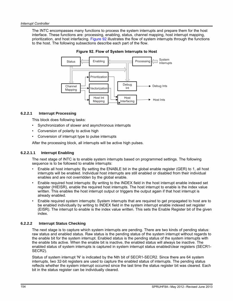
Prioritization
Vectorization
Host IntMapping
ChannelMapping
DebugInt
HostInterfacing
SystemInterrupts
Debug Ints
Host Ints
Enabling ProcessingStatus
Interrupt Controller
The INTC encompasses many functions to process the system interrupts and prepare them for the hostinterface. These functions are: processing, enabling, status, channel mapping, host interrupt mapping,prioritization, and host interfacing. Figure 92 illustrates the flow of system interrupts through the functionsto the host. The following subsections describe each part of the flow.
Figure 92. Flow of System Interrupts to Host
6.2.2.1 Interrupt Processing
This block does following tasks:• Synchronization of slower and asynchronous interrupts• Conversion of polarity to active high• Conversion of interrupt type to pulse interrupts
After the processing block, all interrupts will be active high pulses.
6.2.2.1.1 Interrupt Enabling
The next stage of INTC is to enable system interrupts based on programmed settings. The followingsequence is to be followed to enable interrupts:• Enable all host interrupts: By setting the ENABLE bit in the global enable register (GER) to 1, all host
interrupts will be enabled. Individual host interrupts are still enabled or disabled from their individualenables and are not overridden by the global enable.
• Enable required host interrupts: By writing to the INDEX field in the host interrupt enable indexed setregister (HIEISR), enable the required host interrupts. The host interrupt to enable is the index valuewritten. This enables the host interrupt output or triggers the output again if that host interrupt isalready enabled.
• Enable required system interrupts: System interrupts that are required to get propagated to host are tobe enabled individually by writing to INDEX field in the system interrupt enable indexed set register(EISR). The interrupt to enable is the index value written. This sets the Enable Register bit of the givenindex.
6.2.2.2 Interrupt Status Checking
The next stage is to capture which system interrupts are pending. There are two kinds of pending status:raw status and enabled status. Raw status is the pending status of the system interrupt without regards tothe enable bit for the system interrupt. Enabled status is the pending status of the system interrupts withthe enable bits active. When the enable bit is inactive, the enabled status will always be inactive. Theenabled status of system interrupts is captured in system interrupt status enabled/clear registers (SECR1-SECR2).
Status of system interrupt 'N' is indicated by the Nth bit of SECR1-SECR2. Since there are 64 systeminterrupts, two 32-bit registers are used to capture the enabled status of interrupts. The pending statusreflects whether the system interrupt occurred since the last time the status register bit was cleared. Eachbit in the status register can be individually cleared.
154 SPRUHF8A–May 2012–Revised June 2013

Interrupt Controller
6.2.2.3 Interrupt Channel Mapping
The INTC has 10 internal channels to which enabled system interrupts can be mapped. Channel 0 hashighest priority and channel 9 has the lowest priority. Channels are used to group the system interruptsinto a smaller number of priorities that can be given to a host interface with a very small number ofinterrupt inputs.
When multiple system interrupts are mapped to the same channel their interrupts are ORed together sothat when either is active the output is active. The channel map registers (CMRm) define the channel foreach system interrupt. There is one register per 4 system interrupts; therefore, there are16 channel mapregisters for a system of 64 interrupts. The channel for each system interrupt can be set using theseregisters.
6.2.2.3.1 Host Interrupt Mapping
The hosts can be the PRUs or ARM CPU. The 10 channels from the INTC can mapped to any of the 10Host interrupts. The Host map registers (HMRm) define the channel for each system interrupt. There isone register per 4 channels; therefore, there are 3 host map registers for 10 channels. When multiplechannels are mapped to the same host interrupt, then prioritization is done to select which interrupt is inthe highest-priority channel and which should be sent first to the host.
6.2.2.3.2 Interrupt Prioritization
The next stage of the INTC is prioritization. Since multiple interrupts can feed into a single channel andmultiple channels can feed into a single host interrupt, it is to read the status of all system interrupts todetermine the highest priority interrupt that is pending. The INTC provides hardware to perform thisprioritization with a given scheme so that software does not have to do this. There are two levels ofprioritizations:• The first level of prioritization is between the active channels for a host interrupt. Channel 0 has the
highest priority and channel 9 has the lowest. So the first level of prioritization picks the lowestnumbered active channel.
• The second level of prioritization is between the active system interrupts for the prioritized channel.The system interrupt in position 0 has the highest priority and system interrupt 63 has the lowestpriority. So the second level of prioritization picks the lowest position active system interrupt.
This is the final prioritized system interrupt for the host interrupt and is stored in the global prioritized indexregister (GPIR). The highest priority pending interrupt with respect to each host interrupts can be obtainedusing the host interrupt prioritized index registers (HIPIRn).
6.2.2.4 Interrupt Nesting
The INTC can also perform a nesting function in its prioritization. Nesting is a method of disabling certaininterrupts (usually lower-priority interrupts) when an interrupt is taken so that only those desired interruptscan trigger to the host while it is servicing the current interrupt. The typical usage is to nest on the currentinterrupt and disable all interrupts of the same or lower priority (or channel). Then the host will only beinterrupted from a higher priority interrupt.
The nesting is done in one of three methods:1. Nesting for all host interrupts, based on channel priority: When an interrupt is taken, the nesting level is
set to its channel priority. From then, that channel priority and all lower priority channels will bedisabled from generating host interrupts and only higher priority channels are allowed. When theinterrupt is completely serviced, the nesting level is returned to its original value. When there is nointerrupt being serviced, there are no channels disabled due to nesting. The global nesting levelregister (GNLR) allows the checking and setting of the global nesting level across all host interrupts.The nesting level is the channel (and all of lower priority channels) that are nested out because of acurrent interrupt.
2. Nesting for individual host interrupts, based on channel priority: Always nest based on channel priorityfor each host interrupt individually. When an interrupt is taken on a host interrupt, then, the nestinglevel is set to its channel priority for just that host interrupt, and other host interrupts do not have theirnesting affected. Then for that host interrupt, equal or lower priority channels will not interrupt the hostbut may on other host interrupts if programmed. When the interrupt is completely serviced the nesting
155SPRUHF8A–May 2012–Revised June 2013

Interrupt Controller
level for the host interrupt is returned to its original value. The host interrupt nesting level registers(HINLR1 and HINLR2) display and control the nesting level for each host interrupt. The nesting levelcontrols which channel and lower priority channels are nested. There is one register per host interrupt.
3. Software manually performs the nesting of interrupts. When an interrupt is taken, the software willdisable all the host interrupts, manually update the enables for any or all the system interrupts, andthen re-enables all the host interrupts. This now allows only the system interrupts that are still enabledto trigger to the host. When the interrupt is completely serviced the software must reverse the changesto re-enable the nested out system interrupts. This method requires the most software interaction butgives the most flexibility if simple channel based nesting mechanisms are not adequate.
6.2.2.5 Interrupt Status Clearing
After servicing the interrupt (after execution of the ISR), interrupt status is to be cleared. If a systeminterrupt status is not cleared, then another host interrupt may not be triggered or another host interruptmay be triggered incorrectly. It is also essential to clear all system interrupts before the PRU is halted asthe PRU does not power down unless all the interrupt status are cleared. For clearing the status of aninterrupt, whose interrupt number is N, write a 1 to the Nth bit position in the system interrupt statusenabled/clear registers (SECR1-SECR2). System interrupt N can also be cleared by writing the value Ninto the system interrupt status indexed clear register (SICR).
6.2.3 Interrupt DisablingAt any time, if any interrupt is not to be propagated to the host, then that interrupt should be disabled. Fordisabling an interrupt whose interrupt number is N, write a 1 to the Nth bit in the system interrupt enableclear registers (ECR1-ECR2). System interrupt N can also be disabled by writing the value N in thesystem interrupt enable indexed clear register (EICR).
6.3 Basic Programming Model
Follow these steps to configure the interrupt controller.1. Set polarity and type of system event through the System Interrupt Polarity Registers (SIPR1 and
SPIR2) and the System Interrupt Type Registers (SITR1 and SITR2). Polarity of all system interrupts isalways high. Type of all system interrupts is always pulse.
2. Map system event to INTC channel through CHANMAP registers.3. Map channel to host interrupt through HOSTMAP registers. Recommend channel “x” be mapped to
host interrupt “x”.4. Clear system interrupt by writing 1s to SECR registers.5. Enable host interrupt by writing index value to HOSTINTENIDX register.6. Enable interrupt nesting if desired.7. Globally enable all interrupts through GLBLEN register.
6.4 PRU_ICSS_INTC Registers
Table 100 lists the memory-mapped registers for the PRU_ICSS_INTC. All register offset addresses notlisted in Table 100 should be considered as reserved locations and the register contents should not bemodified.
Table 100. PRU_ICSS_INTC REGISTERSOffset Acronym Register Name Section
0h REVID Section 6.4.14h CR Section 6.4.2
10h GER Section 6.4.31Ch GNLR Section 6.4.420h SISR Section 6.4.524h SICR Section 6.4.628h EISR Section 6.4.7
156 SPRUHF8A–May 2012–Revised June 2013

Interrupt Controller
Table 100. PRU_ICSS_INTC REGISTERS (continued)Offset Acronym Register Name Section2Ch EICR Section 6.4.834h HIEISR Section 6.4.938h HIDISR Section 6.4.1080h GPIR Section 6.4.11200h SRSR0 Section 6.4.12204h SRSR1 Section 6.4.13280h SECR0 Section 6.4.14284h SECR1 Section 6.4.15300h ESR0 Section 6.4.16304h ERS1 Section 6.4.17380h ECR0 Section 6.4.18384h ECR1 Section 6.4.19400h CMR0 Section 6.4.20404h CMR1 Section 6.4.21408h CMR2 Section 6.4.2240Ch CMR3 Section 6.4.23410h CMR4 Section 6.4.24414h CMR5 Section 6.4.25418h CMR6 Section 6.4.2641Ch CMR7 Section 6.4.27420h CMR8 Section 6.4.28424h CMR9 Section 6.4.29428h CMR10 Section 6.4.3042Ch CMR11 Section 6.4.31430h CMR12 Section 6.4.32434h CMR13 Section 6.4.33438h CMR14 Section 6.4.3443Ch CMR15 Section 6.4.35800h HMR0 Section 6.4.36804h HMR1 Section 6.4.37808h HMR2 Section 6.4.38900h HIPIR0 Section 6.4.39904h HIPIR1 Section 6.4.40908h HIPIR2 Section 6.4.4190Ch HIPIR3 Section 6.4.42910h HIPIR4 Section 6.4.43914h HIPIR5 Section 6.4.44918h HIPIR6 Section 6.4.4591Ch HIPIR7 Section 6.4.46920h HIPIR8 Section 6.4.47924h HIPIR9 Section 6.4.48D00h SIPR0 Section 6.4.49D04h SIPR1 Section 6.4.50D80h SITR0 Section 6.4.51D84h SITR1 Section 6.4.521100h HINLR0 Section 6.4.531104h HINLR1 Section 6.4.54
157SPRUHF8A–May 2012–Revised June 2013

Interrupt Controller
Table 100. PRU_ICSS_INTC REGISTERS (continued)Offset Acronym Register Name Section1108h HINLR2 Section 6.4.55110Ch HINLR3 Section 6.4.561110h HINLR4 Section 6.4.571114h HINLR5 Section 6.4.581118h HINLR6 Section 6.4.59111Ch HINLR7 Section 6.4.601120h HINLR8 Section 6.4.611124h HINLR9 Section 6.4.621500h HIER Section 6.4.63
158 SPRUHF8A–May 2012–Revised June 2013

Interrupt Controller
6.4.1 REVID Register (offset = 0h) [reset = 4E82A900h]REVID is shown in Figure 93 and described in Table 101.
Revision ID Register
Figure 93. REVID Register31 30 29 28 27 26 25 24
REV_SCHEME Reserved REV_MODULE
R-1h R-E82h
23 22 21 20 19 18 17 16
REV_MODULE
R-E82h
15 14 13 12 11 10 9 8
REV_RTL REV_MAJOR
R-15h R-1h
7 6 5 4 3 2 1 0
REV_CUSTOM REV_MINOR
R-0h R-0h
LEGEND: R/W = Read/Write; R = Read only; W1toCl = Write 1 to clear bit; -n = value after reset
Table 101. REVID Register Field Descriptions
Bit Field Type Reset Description31-30 REV_SCHEME R 1h SCHEME27-16 REV_MODULE R E82h MODULE ID15-11 REV_RTL R 15h RTL REVISIONS10-8 REV_MAJOR R 1h MAJOR REVISION7-6 REV_CUSTOM R 0h CUSTOM REVISION5-0 REV_MINOR R 0h MINOR REVISION
159SPRUHF8A–May 2012–Revised June 2013

Interrupt Controller
6.4.2 CR Register (offset = 4h) [reset = 0h]CR is shown in Figure 94 and described in Table 102.
The Control Register holds global control parameters and can forces a soft reset on the module.
Figure 94. CR Register31 30 29 28 27 26 25 24
Reserved
23 22 21 20 19 18 17 16
Reserved
15 14 13 12 11 10 9 8
Reserved
7 6 5 4 3 2 1 0
Reserved Reserved NEST_MODE Reserved Reserved
R-0h R/W-0h R/W-0h
LEGEND: R/W = Read/Write; R = Read only; W1toCl = Write 1 to clear bit; -n = value after reset
Table 102. CR Register Field Descriptions
Bit Field Type Reset Description4 Reserved R 0h Reserved.
3-2 NEST_MODE R/W 0h The nesting mode.0 = no nesting1 = automatic individual nesting (per host interrupt)2 = automatic global nesting (over all host interrupts)3 = manual nesting
1 Reserved R/W 0h Reserved.
160 SPRUHF8A–May 2012–Revised June 2013

Interrupt Controller
6.4.3 GER Register (offset = 10h) [reset = 0h]GER is shown in Figure 95 and described in Table 103.
The Global Host Interrupt Enable Register enables all the host interrupts. Individual host interrupts are stillenabled or disabled from their individual enables and are not overridden by the global enable.
Figure 95. GER Register31 30 29 28 27 26 25 24 23 22 21 20 19 18 17 16 15 14 13 12 11 10 9 8 7 6 5 4 3 2 1 0
Reserved ENABLE_HINT_ANY
R/W-0h
LEGEND: R/W = Read/Write; R = Read only; W1toCl = Write 1 to clear bit; -n = value after reset
Table 103. GER Register Field Descriptions
Bit Field Type Reset Description0 ENABLE_HINT_ANY R/W 0h The current global enable value when read.
Writes set the global enable.
161SPRUHF8A–May 2012–Revised June 2013

Interrupt Controller
6.4.4 GNLR Register (offset = 1Ch) [reset = 100h]GNLR is shown in Figure 96 and described in Table 104.
The Global Nesting Level Register allows the checking and setting of the global nesting level across allhost interrupts when automatic global nesting mode is set. The nesting level is the channel (and all oflower priority) that are nested out because of a current interrupt. This register is only available whennesting is configured.
Figure 96. GNLR Register31 30 29 28 27 26 25 24
AUTO_OVERRIDE Reserved
W-0h
23 22 21 20 19 18 17 16
Reserved
15 14 13 12 11 10 9 8
Reserved GLB_NEST_LEVEL
R/W-100h
7 6 5 4 3 2 1 0
GLB_NEST_LEVEL
R/W-100h
LEGEND: R/W = Read/Write; R = Read only; W1toCl = Write 1 to clear bit; -n = value after reset
Table 104. GNLR Register Field Descriptions
Bit Field Type Reset Description31 AUTO_OVERRIDE W 0h Always read as 0.
Writes of 1 override the automatic nesting and set the nesting_levelto the written data.
8-0 GLB_NEST_LEVEL R/W 100h The current global nesting level (highest channel that is nested).Writes set the nesting level.In auto nesting mode this value is updated internally unless theauto_override bit is set.
162 SPRUHF8A–May 2012–Revised June 2013

Interrupt Controller
6.4.5 SISR Register (offset = 20h) [reset = 0h]SISR is shown in Figure 97 and described in Table 105.
The System Interrupt Status Indexed Set Register allows setting the status of an interrupt. The interrupt toset is the index value written. This sets the Raw Status Register bit of the given index.
Figure 97. SISR Register31 30 29 28 27 26 25 24 23 22 21 20 19 18 17 16 15 14 13 12 11 10 9 8 7 6 5 4 3 2 1 0
Reserved STATUS_SET_INDEX
W-0h
LEGEND: R/W = Read/Write; R = Read only; W1toCl = Write 1 to clear bit; -n = value after reset
Table 105. SISR Register Field Descriptions
Bit Field Type Reset Description9-0 STATUS_SET_INDEX W 0h Writes set the status of the interrupt given in the index value.
Reads return 0.
163SPRUHF8A–May 2012–Revised June 2013

Interrupt Controller
6.4.6 SICR Register (offset = 24h) [reset = 0h]SICR is shown in Figure 98 and described in Table 106.
The System Interrupt Status Indexed Clear Register allows clearing the status of an interrupt. Theinterrupt to clear is the index value written. This clears the Raw Status Register bit of the given index.
Figure 98. SICR Register31 30 29 28 27 26 25 24 23 22 21 20 19 18 17 16 15 14 13 12 11 10 9 8 7 6 5 4 3 2 1 0
Reserved STATUS_CLR_INDEX
W-0h
LEGEND: R/W = Read/Write; R = Read only; W1toCl = Write 1 to clear bit; -n = value after reset
Table 106. SICR Register Field Descriptions
Bit Field Type Reset Description9-0 STATUS_CLR_INDEX W 0h Writes clear the status of the interrupt given in the index value.
Reads return 0.
164 SPRUHF8A–May 2012–Revised June 2013

Interrupt Controller
6.4.7 EISR Register (offset = 28h) [reset = 0h]EISR is shown in Figure 99 and described in Table 107.
The System Interrupt Enable Indexed Set Register allows enabling an interrupt. The interrupt to enable isthe index value written. This sets the Enable Register bit of the given index.
Figure 99. EISR Register31 30 29 28 27 26 25 24 23 22 21 20 19 18 17 16 15 14 13 12 11 10 9 8 7 6 5 4 3 2 1 0
Reserved ENABLE_SET_INDEX
W-0h
LEGEND: R/W = Read/Write; R = Read only; W1toCl = Write 1 to clear bit; -n = value after reset
Table 107. EISR Register Field Descriptions
Bit Field Type Reset Description9-0 ENABLE_SET_INDEX W 0h Writes set the enable of the interrupt given in the index value.
Reads return 0.
165SPRUHF8A–May 2012–Revised June 2013

Interrupt Controller
6.4.8 EICR Register (offset = 2Ch) [reset = 0h]EICR is shown in Figure 100 and described in Table 108.
The System Interrupt Enable Indexed Clear Register allows disabling an interrupt. The interrupt to disableis the index value written. This clears the Enable Register bit of the given index.
Figure 100. EICR Register31 30 29 28 27 26 25 24 23 22 21 20 19 18 17 16 15 14 13 12 11 10 9 8 7 6 5 4 3 2 1 0
Reserved ENABLE_CLR_INDEX
W-0h
LEGEND: R/W = Read/Write; R = Read only; W1toCl = Write 1 to clear bit; -n = value after reset
Table 108. EICR Register Field Descriptions
Bit Field Type Reset Description9-0 ENABLE_CLR_INDEX W 0h Writes clear the enable of the interrupt given in the index value.
Reads return 0.
166 SPRUHF8A–May 2012–Revised June 2013

Interrupt Controller
6.4.9 HIEISR Register (offset = 34h) [reset = 0h]HIEISR is shown in Figure 101 and described in Table 109.
The Host Interrupt Enable Indexed Set Register allows enabling a host interrupt output. The host interruptto enable is the index value written. This enables the host interrupt output or triggers the output again ifalready enabled.
Figure 101. HIEISR Register31 30 29 28 27 26 25 24 23 22 21 20 19 18 17 16 15 14 13 12 11 10 9 8 7 6 5 4 3 2 1 0
Reserved HINT_ENABLE_SET_INDEX
R/W-0h
LEGEND: R/W = Read/Write; R = Read only; W1toCl = Write 1 to clear bit; -n = value after reset
Table 109. HIEISR Register Field Descriptions
Bit Field Type Reset Description9-0 HINT_ENABLE_SET_IND R/W 0h Writes set the enable of the host interrupt given in the index value.
EX Reads return 0.
167SPRUHF8A–May 2012–Revised June 2013

Interrupt Controller
6.4.10 HIDISR Register (offset = 38h) [reset = 0h]HIDISR is shown in Figure 102 and described in Table 110.
The Host Interrupt Enable Indexed Clear Register allows disabling a host interrupt output. The hostinterrupt to disable is the index value written. This disables the host interrupt output.
Figure 102. HIDISR Register31 30 29 28 27 26 25 24 23 22 21 20 19 18 17 16 15 14 13 12 11 10 9 8 7 6 5 4 3 2 1 0
Reserved HINT_ENABLE_CLR_INDEX
R/W-0h
LEGEND: R/W = Read/Write; R = Read only; W1toCl = Write 1 to clear bit; -n = value after reset
Table 110. HIDISR Register Field Descriptions
Bit Field Type Reset Description9-0 HINT_ENABLE_CLR_IND R/W 0h Writes clear the enable of the host interrupt given in the index value.
EX Reads return 0.
168 SPRUHF8A–May 2012–Revised June 2013

Interrupt Controller
6.4.11 GPIR Register (offset = 80h) [reset = 80000000h]GPIR is shown in Figure 103 and described in Table 111.
The Global Prioritized Index Register shows the interrupt number of the highest priority interrupt pendingacross all the host interrupts.
Figure 103. GPIR Register31 30 29 28 27 26 25 24
GLB_NONE Reserved
R-1h
23 22 21 20 19 18 17 16
Reserved
15 14 13 12 11 10 9 8
Reserved GLB_PRI_INTR
R-0h
7 6 5 4 3 2 1 0
GLB_PRI_INTR
R-0h
LEGEND: R/W = Read/Write; R = Read only; W1toCl = Write 1 to clear bit; -n = value after reset
Table 111. GPIR Register Field Descriptions
Bit Field Type Reset Description31 GLB_NONE R 1h No Interrupt is pending.
Can be used by host to test for a negative value to see if nointerrupts are pending.
9-0 GLB_PRI_INTR R 0h The currently highest priority interrupt index pending across all thehost interrupts.
169SPRUHF8A–May 2012–Revised June 2013

Interrupt Controller
6.4.12 SRSR0 Register (offset = 200h) [reset = 0h]SRSR0 is shown in Figure 104 and described in Table 112.
The System Interrupt Status Raw/Set Register0 show the pending enabled status of the system interrupts0 to 31. Software can write to the Status Set Registers to set a system interrupt without a hardwaretrigger. There is one bit per system interrupt.
Figure 104. SRSR0 Register31 30 29 28 27 26 25 24 23 22 21 20 19 18 17 16 15 14 13 12 11 10 9 8 7 6 5 4 3 2 1 0
RAW_STATUS_31_0
R/W-0h
LEGEND: R/W = Read/Write; R = Read only; W1toCl = Write 1 to clear bit; -n = value after reset
Table 112. SRSR0 Register Field Descriptions
Bit Field Type Reset Description31-0 RAW_STATUS_31_0 R/W 0h System interrupt raw status and setting of the system interrupts 0 to
31.Reads return the raw status.Write a 1 in a bit position to set the status of the system interrupt.Writing a 0 has no effect.
170 SPRUHF8A–May 2012–Revised June 2013

Interrupt Controller
6.4.13 SRSR1 Register (offset = 204h) [reset = 0h]SRSR1 is shown in Figure 105 and described in Table 113.
The System Interrupt Status Raw/Set Register1 show the pending enabled status of the system interrupts32 to 63. Software can write to the Status Set Registers to set a system interrupt without a hardwaretrigger. There is one bit per system interrupt.
Figure 105. SRSR1 Register31 30 29 28 27 26 25 24 23 22 21 20 19 18 17 16 15 14 13 12 11 10 9 8 7 6 5 4 3 2 1 0
RAW_STATUS_63_32
R/W-0h
LEGEND: R/W = Read/Write; R = Read only; W1toCl = Write 1 to clear bit; -n = value after reset
Table 113. SRSR1 Register Field Descriptions
Bit Field Type Reset Description31-0 RAW_STATUS_63_32 R/W 0h System interrupt raw status and setting of the system interrupts 32 to
63.Reads return the raw status.Write a 1 in a bit position to set the status of the system interrupt.Writing a 0 has no effect.
171SPRUHF8A–May 2012–Revised June 2013

Interrupt Controller
6.4.14 SECR0 Register (offset = 280h) [reset = 0h]SECR0 is shown in Figure 106 and described in Table 114.
The System Interrupt Status Enabled/Clear Register0 show the pending enabled status of the systeminterrupts 0 to 31. Software can write to the Status Clear Registers to clear a system interrupt after it hasbeen serviced. If a system interrupt status is not cleared then another host interrupt may not be triggeredor another host interrupt may be triggered incorrectly. There is one bit per system interrupt.
Figure 106. SECR0 Register31 30 29 28 27 26 25 24 23 22 21 20 19 18 17 16 15 14 13 12 11 10 9 8 7 6 5 4 3 2 1 0
ENA_STATUS_31_0
R/W-0h
LEGEND: R/W = Read/Write; R = Read only; W1toCl = Write 1 to clear bit; -n = value after reset
Table 114. SECR0 Register Field Descriptions
Bit Field Type Reset Description31-0 ENA_STATUS_31_0 R/W 0h System interrupt enabled status and clearing of the system interrupts
0 to 31.Reads return the enabled status (before enabling with the EnableRegisters).Write a 1 in a bit position to clear the status of the system interrupt.Writing a 0 has no effect.
172 SPRUHF8A–May 2012–Revised June 2013

Interrupt Controller
6.4.15 SECR1 Register (offset = 284h) [reset = 0h]SECR1 is shown in Figure 107 and described in Table 115.
The System Interrupt Status Enabled/Clear Register1 show the pending enabled status of the systeminterrupts 32 to 63. Software can write to the Status Clear Registers to clear a system interrupt after it hasbeen serviced. If a system interrupt status is not cleared then another host interrupt may not be triggeredor another host interrupt may be triggered incorrectly. There is one bit per system interrupt.
Figure 107. SECR1 Register31 30 29 28 27 26 25 24 23 22 21 20 19 18 17 16 15 14 13 12 11 10 9 8 7 6 5 4 3 2 1 0
ENA_STATUS_63_32
R/W-0h
LEGEND: R/W = Read/Write; R = Read only; W1toCl = Write 1 to clear bit; -n = value after reset
Table 115. SECR1 Register Field Descriptions
Bit Field Type Reset Description31-0 ENA_STATUS_63_32 R/W 0h System interrupt enabled status and clearing of the system interrupts
32 to 63.Reads return the enabled status (before enabling with the EnableRegisters).Write a 1 in a bit position to clear the status of the system interrupt.Writing a 0 has no effect.
173SPRUHF8A–May 2012–Revised June 2013

Interrupt Controller
6.4.16 ESR0 Register (offset = 300h) [reset = 0h]ESR0 is shown in Figure 108 and described in Table 116.
The System Interrupt Enable Set Register0 enables system interrupts 0 to 31 to trigger outputs. Systeminterrupts that are not enabled do not interrupt the host. There is a bit per system interrupt.
Figure 108. ESR0 Register31 30 29 28 27 26 25 24 23 22 21 20 19 18 17 16 15 14 13 12 11 10 9 8 7 6 5 4 3 2 1 0
ENABLE_SET_31_0
0h
LEGEND: R/W = Read/Write; R = Read only; W1toCl = Write 1 to clear bit; -n = value after reset
Table 116. ESR0 Register Field Descriptions
Bit Field Type Reset Description31-0 ENABLE_SET_31_0 0h System interrupt enables system interrupts 0 to 31.
Read returns the enable value (0 = disabled,1 = enabled).Write a 1 in a bit position to set that enable.Writing a 0 has no effect.
174 SPRUHF8A–May 2012–Revised June 2013

Interrupt Controller
6.4.17 ERS1 Register (offset = 304h) [reset = 0h]ERS1 is shown in Figure 109 and described in Table 117.
The System Interrupt Enable Set Register1 enables system interrupts 32 to 63 to trigger outputs. Systeminterrupts that are not enabled do not interrupt the host. There is a bit per system interrupt.
Figure 109. ERS1 Register31 30 29 28 27 26 25 24 23 22 21 20 19 18 17 16 15 14 13 12 11 10 9 8 7 6 5 4 3 2 1 0
ENABLE_SET_63_32
0h
LEGEND: R/W = Read/Write; R = Read only; W1toCl = Write 1 to clear bit; -n = value after reset
Table 117. ERS1 Register Field Descriptions
Bit Field Type Reset Description31-0 ENABLE_SET_63_32 0h System interrupt enables system interrupts 32 to 63.
Read returns the enable value (0 = disabled,1 = enabled).Write a 1 in a bit position to set that enable.Writing a 0 has no effect.
175SPRUHF8A–May 2012–Revised June 2013

Interrupt Controller
6.4.18 ECR0 Register (offset = 380h) [reset = 0h]ECR0 is shown in Figure 110 and described in Table 118.
The System Interrupt Enable Clear Register0 disables system interrupts 0 to 31 to map to channels.System interrupts that are not enabled do not interrupt the host. There is a bit per system interrupt.
Figure 110. ECR0 Register31 30 29 28 27 26 25 24 23 22 21 20 19 18 17 16 15 14 13 12 11 10 9 8 7 6 5 4 3 2 1 0
ENABLE_CLR_31_0
0h
LEGEND: R/W = Read/Write; R = Read only; W1toCl = Write 1 to clear bit; -n = value after reset
Table 118. ECR0 Register Field Descriptions
Bit Field Type Reset Description31-0 ENABLE_CLR_31_0 0h System interrupt enables system interrupts 0 to 31.
Read returns the enable value (0 = disabled,1 = enabled).Write a 1 in a bit position to clear that enable.Writing a 0 has no effect.
176 SPRUHF8A–May 2012–Revised June 2013

Interrupt Controller
6.4.19 ECR1 Register (offset = 384h) [reset = 0h]ECR1 is shown in Figure 111 and described in Table 119.
The System Interrupt Enable Clear Register1 disables system interrupts 32 to 63 to map to channels.System interrupts that are not enabled do not interrupt the host. There is a bit per system interrupt.
Figure 111. ECR1 Register31 30 29 28 27 26 25 24 23 22 21 20 19 18 17 16 15 14 13 12 11 10 9 8 7 6 5 4 3 2 1 0
ENABLE_CLR_63_32
0h
LEGEND: R/W = Read/Write; R = Read only; W1toCl = Write 1 to clear bit; -n = value after reset
Table 119. ECR1 Register Field Descriptions
Bit Field Type Reset Description31-0 ENABLE_CLR_63_32 0h System interrupt enables system interrupts 32 to 63.
Read returns the enable value (0 = disabled,1 = enabled).Write a 1 in a bit position to clear that enable.Writing a 0 has no effect.
177SPRUHF8A–May 2012–Revised June 2013

Interrupt Controller
6.4.20 CMR0 Register (offset = 400h) [reset = 0h]CMR0 is shown in Figure 112 and described in Table 120.
The Channel Map Register0 specify the channel for the system interrupts 0 to 3. There is one register per4 system interrupts.
Figure 112. CMR0 Register31 30 29 28 27 26 25 24
Reserved CH_MAP_3
R/W-0h
23 22 21 20 19 18 17 16
Reserved CH_MAP_2
R/W-0h
15 14 13 12 11 10 9 8
Reserved CH_MAP_1
R/W-0h
7 6 5 4 3 2 1 0
Reserved CH_MAP_0
R/W-0h
LEGEND: R/W = Read/Write; R = Read only; W1toCl = Write 1 to clear bit; -n = value after reset
Table 120. CMR0 Register Field Descriptions
Bit Field Type Reset Description27-24 CH_MAP_3 R/W 0h Sets the channel for the system interrupt 319-16 CH_MAP_2 R/W 0h Sets the channel for the system interrupt 211-8 CH_MAP_1 R/W 0h Sets the channel for the system interrupt 13-0 CH_MAP_0 R/W 0h Sets the channel for the system interrupt 0
178 SPRUHF8A–May 2012–Revised June 2013

Interrupt Controller
6.4.21 CMR1 Register (offset = 404h) [reset = 0h]CMR1 is shown in Figure 113 and described in Table 121.
The Channel Map Register1 specify the channel for the system interrupts 4 to 7. There is one register per4 system interrupts.
Figure 113. CMR1 Register31 30 29 28 27 26 25 24
Reserved CH_MAP_7
R/W-0h
23 22 21 20 19 18 17 16
Reserved CH_MAP_6
R/W-0h
15 14 13 12 11 10 9 8
Reserved CH_MAP_5
R/W-0h
7 6 5 4 3 2 1 0
Reserved CH_MAP_4
R/W-0h
LEGEND: R/W = Read/Write; R = Read only; W1toCl = Write 1 to clear bit; -n = value after reset
Table 121. CMR1 Register Field Descriptions
Bit Field Type Reset Description27-24 CH_MAP_7 R/W 0h Sets the channel for the system interrupt 719-16 CH_MAP_6 R/W 0h Sets the channel for the system interrupt 611-8 CH_MAP_5 R/W 0h Sets the channel for the system interrupt 53-0 CH_MAP_4 R/W 0h Sets the channel for the system interrupt 4
179SPRUHF8A–May 2012–Revised June 2013

Interrupt Controller
6.4.22 CMR2 Register (offset = 408h) [reset = 0h]CMR2 is shown in Figure 114 and described in Table 122.
The Channel Map Register2 specify the channel for the system interrupts 8 to 11. There is one registerper 4 system interrupts.
Figure 114. CMR2 Register31 30 29 28 27 26 25 24
Reserved CH_MAP_11
R/W-0h
23 22 21 20 19 18 17 16
Reserved CH_MAP_10
R/W-0h
15 14 13 12 11 10 9 8
Reserved CH_MAP_9
R/W-0h
7 6 5 4 3 2 1 0
Reserved CH_MAP_8
R/W-0h
LEGEND: R/W = Read/Write; R = Read only; W1toCl = Write 1 to clear bit; -n = value after reset
Table 122. CMR2 Register Field Descriptions
Bit Field Type Reset Description27-24 CH_MAP_11 R/W 0h Sets the channel for the system interrupt 1119-16 CH_MAP_10 R/W 0h Sets the channel for the system interrupt 1011-8 CH_MAP_9 R/W 0h Sets the channel for the system interrupt 93-0 CH_MAP_8 R/W 0h Sets the channel for the system interrupt 8
180 SPRUHF8A–May 2012–Revised June 2013

Interrupt Controller
6.4.23 CMR3 Register (offset = 40Ch) [reset = 0h]CMR3 is shown in Figure 115 and described in Table 123.
The Channel Map Register3 specify the channel for the system interrupts 12 to 15. There is one registerper 4 system interrupts.
Figure 115. CMR3 Register31 30 29 28 27 26 25 24
Reserved CH_MAP_15
R/W-0h
23 22 21 20 19 18 17 16
Reserved CH_MAP_14
R/W-0h
15 14 13 12 11 10 9 8
Reserved CH_MAP_13
R/W-0h
7 6 5 4 3 2 1 0
Reserved CH_MAP_12
R/W-0h
LEGEND: R/W = Read/Write; R = Read only; W1toCl = Write 1 to clear bit; -n = value after reset
Table 123. CMR3 Register Field Descriptions
Bit Field Type Reset Description27-24 CH_MAP_15 R/W 0h Sets the channel for the system interrupt 1519-16 CH_MAP_14 R/W 0h Sets the channel for the system interrupt 1411-8 CH_MAP_13 R/W 0h Sets the channel for the system interrupt 133-0 CH_MAP_12 R/W 0h Sets the channel for the system interrupt 12
181SPRUHF8A–May 2012–Revised June 2013

Interrupt Controller
6.4.24 CMR4 Register (offset = 410h) [reset = 0h]CMR4 is shown in Figure 116 and described in Table 124.
The Channel Map Register4 specify the channel for the system interrupts 16 to 19. There is one registerper 4 system interrupts.
Figure 116. CMR4 Register31 30 29 28 27 26 25 24
Reserved CH_MAP_19
R/W-0h
23 22 21 20 19 18 17 16
Reserved CH_MAP_18
R/W-0h
15 14 13 12 11 10 9 8
Reserved CH_MAP_17
R/W-0h
7 6 5 4 3 2 1 0
Reserved CH_MAP_16
R/W-0h
LEGEND: R/W = Read/Write; R = Read only; W1toCl = Write 1 to clear bit; -n = value after reset
Table 124. CMR4 Register Field Descriptions
Bit Field Type Reset Description27-24 CH_MAP_19 R/W 0h Sets the channel for the system interrupt 1919-16 CH_MAP_18 R/W 0h Sets the channel for the system interrupt 1811-8 CH_MAP_17 R/W 0h Sets the channel for the system interrupt 173-0 CH_MAP_16 R/W 0h Sets the channel for the system interrupt 16
182 SPRUHF8A–May 2012–Revised June 2013

Interrupt Controller
6.4.25 CMR5 Register (offset = 414h) [reset = 0h]CMR5 is shown in Figure 117 and described in Table 125.
The Channel Map Register5 specify the channel for the system interrupts 20 to 23. There is one registerper 4 system interrupts.
Figure 117. CMR5 Register31 30 29 28 27 26 25 24
Reserved CH_MAP_23
R/W-0h
23 22 21 20 19 18 17 16
Reserved CH_MAP_22
R/W-0h
15 14 13 12 11 10 9 8
Reserved CH_MAP_21
R/W-0h
7 6 5 4 3 2 1 0
Reserved CH_MAP_20
R/W-0h
LEGEND: R/W = Read/Write; R = Read only; W1toCl = Write 1 to clear bit; -n = value after reset
Table 125. CMR5 Register Field Descriptions
Bit Field Type Reset Description27-24 CH_MAP_23 R/W 0h Sets the channel for the system interrupt 2319-16 CH_MAP_22 R/W 0h Sets the channel for the system interrupt 2211-8 CH_MAP_21 R/W 0h Sets the channel for the system interrupt 213-0 CH_MAP_20 R/W 0h Sets the channel for the system interrupt 20
183SPRUHF8A–May 2012–Revised June 2013

Interrupt Controller
6.4.26 CMR6 Register (offset = 418h) [reset = 0h]CMR6 is shown in Figure 118 and described in Table 126.
The Channel Map Register6 specify the channel for the system interrupts 24 to 27. There is one registerper 4 system interrupts.
Figure 118. CMR6 Register31 30 29 28 27 26 25 24
Reserved CH_MAP_27
R/W-0h
23 22 21 20 19 18 17 16
Reserved CH_MAP_26
R/W-0h
15 14 13 12 11 10 9 8
Reserved CH_MAP_25
R/W-0h
7 6 5 4 3 2 1 0
Reserved CH_MAP_24
R/W-0h
LEGEND: R/W = Read/Write; R = Read only; W1toCl = Write 1 to clear bit; -n = value after reset
Table 126. CMR6 Register Field Descriptions
Bit Field Type Reset Description27-24 CH_MAP_27 R/W 0h Sets the channel for the system interrupt 2719-16 CH_MAP_26 R/W 0h Sets the channel for the system interrupt 2611-8 CH_MAP_25 R/W 0h Sets the channel for the system interrupt 253-0 CH_MAP_24 R/W 0h Sets the channel for the system interrupt 24
184 SPRUHF8A–May 2012–Revised June 2013

Interrupt Controller
6.4.27 CMR7 Register (offset = 41Ch) [reset = 0h]CMR7 is shown in Figure 119 and described in Table 127.
The Channel Map Register7 specify the channel for the system interrupts 28 to 31. There is one registerper 4 system interrupts.
Figure 119. CMR7 Register31 30 29 28 27 26 25 24
Reserved CH_MAP_31
R/W-0h
23 22 21 20 19 18 17 16
Reserved CH_MAP_30
R/W-0h
15 14 13 12 11 10 9 8
Reserved CH_MAP_29
R/W-0h
7 6 5 4 3 2 1 0
Reserved CH_MAP_28
R/W-0h
LEGEND: R/W = Read/Write; R = Read only; W1toCl = Write 1 to clear bit; -n = value after reset
Table 127. CMR7 Register Field Descriptions
Bit Field Type Reset Description27-24 CH_MAP_31 R/W 0h Sets the channel for the system interrupt 3119-16 CH_MAP_30 R/W 0h Sets the channel for the system interrupt 3011-8 CH_MAP_29 R/W 0h Sets the channel for the system interrupt 293-0 CH_MAP_28 R/W 0h Sets the channel for the system interrupt 28
185SPRUHF8A–May 2012–Revised June 2013

Interrupt Controller
6.4.28 CMR8 Register (offset = 420h) [reset = 0h]CMR8 is shown in Figure 120 and described in Table 128.
The Channel Map Register8 specify the channel for the system interrupts 32 to 35. There is one registerper 4 system interrupts.
Figure 120. CMR8 Register31 30 29 28 27 26 25 24
Reserved CH_MAP_35
R/W-0h
23 22 21 20 19 18 17 16
Reserved CH_MAP_34
R/W-0h
15 14 13 12 11 10 9 8
Reserved CH_MAP_33
R/W-0h
7 6 5 4 3 2 1 0
Reserved CH_MAP_32
R/W-0h
LEGEND: R/W = Read/Write; R = Read only; W1toCl = Write 1 to clear bit; -n = value after reset
Table 128. CMR8 Register Field Descriptions
Bit Field Type Reset Description27-24 CH_MAP_35 R/W 0h Sets the channel for the system interrupt 3519-16 CH_MAP_34 R/W 0h Sets the channel for the system interrupt 3411-8 CH_MAP_33 R/W 0h Sets the channel for the system interrupt 333-0 CH_MAP_32 R/W 0h Sets the channel for the system interrupt 32
186 SPRUHF8A–May 2012–Revised June 2013

Interrupt Controller
6.4.29 CMR9 Register (offset = 424h) [reset = 0h]CMR9 is shown in Figure 121 and described in Table 129.
The Channel Map Register9 specify the channel for the system interrupts 36 to 39. There is one registerper 4 system interrupts.
Figure 121. CMR9 Register31 30 29 28 27 26 25 24
Reserved CH_MAP_39
R/W-0h
23 22 21 20 19 18 17 16
Reserved CH_MAP_38
R/W-0h
15 14 13 12 11 10 9 8
Reserved CH_MAP_37
R/W-0h
7 6 5 4 3 2 1 0
Reserved CH_MAP_36
R/W-0h
LEGEND: R/W = Read/Write; R = Read only; W1toCl = Write 1 to clear bit; -n = value after reset
Table 129. CMR9 Register Field Descriptions
Bit Field Type Reset Description27-24 CH_MAP_39 R/W 0h Sets the channel for the system interrupt 3919-16 CH_MAP_38 R/W 0h Sets the channel for the system interrupt 3811-8 CH_MAP_37 R/W 0h Sets the channel for the system interrupt 373-0 CH_MAP_36 R/W 0h Sets the channel for the system interrupt 36
187SPRUHF8A–May 2012–Revised June 2013
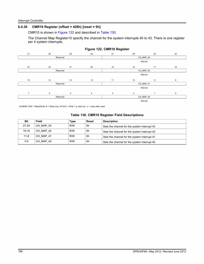
Interrupt Controller
6.4.30 CMR10 Register (offset = 428h) [reset = 0h]CMR10 is shown in Figure 122 and described in Table 130.
The Channel Map Register10 specify the channel for the system interrupts 40 to 43. There is one registerper 4 system interrupts.
Figure 122. CMR10 Register31 30 29 28 27 26 25 24
Reserved CH_MAP_43
R/W-0h
23 22 21 20 19 18 17 16
Reserved CH_MAP_42
R/W-0h
15 14 13 12 11 10 9 8
Reserved CH_MAP_41
R/W-0h
7 6 5 4 3 2 1 0
Reserved CH_MAP_40
R/W-0h
LEGEND: R/W = Read/Write; R = Read only; W1toCl = Write 1 to clear bit; -n = value after reset
Table 130. CMR10 Register Field Descriptions
Bit Field Type Reset Description27-24 CH_MAP_43 R/W 0h Sets the channel for the system interrupt 4319-16 CH_MAP_42 R/W 0h Sets the channel for the system interrupt 4211-8 CH_MAP_41 R/W 0h Sets the channel for the system interrupt 413-0 CH_MAP_40 R/W 0h Sets the channel for the system interrupt 40
188 SPRUHF8A–May 2012–Revised June 2013

Interrupt Controller
6.4.31 CMR11 Register (offset = 42Ch) [reset = 0h]CMR11 is shown in Figure 123 and described in Table 131.
The Channel Map Register11 specify the channel for the system interrupts 44 to 47. There is one registerper 4 system interrupts.
Figure 123. CMR11 Register31 30 29 28 27 26 25 24
Reserved CH_MAP_47
R/W-0h
23 22 21 20 19 18 17 16
Reserved CH_MAP_46
R/W-0h
15 14 13 12 11 10 9 8
Reserved CH_MAP_45
R/W-0h
7 6 5 4 3 2 1 0
Reserved CH_MAP_44
R/W-0h
LEGEND: R/W = Read/Write; R = Read only; W1toCl = Write 1 to clear bit; -n = value after reset
Table 131. CMR11 Register Field Descriptions
Bit Field Type Reset Description27-24 CH_MAP_47 R/W 0h Sets the channel for the system interrupt 4719-16 CH_MAP_46 R/W 0h Sets the channel for the system interrupt 4611-8 CH_MAP_45 R/W 0h Sets the channel for the system interrupt 453-0 CH_MAP_44 R/W 0h Sets the channel for the system interrupt 44
189SPRUHF8A–May 2012–Revised June 2013

Interrupt Controller
6.4.32 CMR12 Register (offset = 430h) [reset = 0h]CMR12 is shown in Figure 124 and described in Table 132.
The Channel Map Register12 specify the channel for the system interrupts 48 to 51. There is one registerper 4 system interrupts.
Figure 124. CMR12 Register31 30 29 28 27 26 25 24
Reserved CH_MAP_51
R/W-0h
23 22 21 20 19 18 17 16
Reserved CH_MAP_50
R/W-0h
15 14 13 12 11 10 9 8
Reserved CH_MAP_49
R/W-0h
7 6 5 4 3 2 1 0
Reserved CH_MAP_48
R/W-0h
LEGEND: R/W = Read/Write; R = Read only; W1toCl = Write 1 to clear bit; -n = value after reset
Table 132. CMR12 Register Field Descriptions
Bit Field Type Reset Description27-24 CH_MAP_51 R/W 0h Sets the channel for the system interrupt 5119-16 CH_MAP_50 R/W 0h Sets the channel for the system interrupt 5011-8 CH_MAP_49 R/W 0h Sets the channel for the system interrupt 493-0 CH_MAP_48 R/W 0h Sets the channel for the system interrupt 48
190 SPRUHF8A–May 2012–Revised June 2013

Interrupt Controller
6.4.33 CMR13 Register (offset = 434h) [reset = 0h]CMR13 is shown in Figure 125 and described in Table 133.
The Channel Map Register13 specify the channel for the system interrupts 52 to 55. There is one registerper 4 system interrupts.
Figure 125. CMR13 Register31 30 29 28 27 26 25 24
Reserved CH_MAP_55
R/W-0h
23 22 21 20 19 18 17 16
Reserved CH_MAP_54
R/W-0h
15 14 13 12 11 10 9 8
Reserved CH_MAP_53
R/W-0h
7 6 5 4 3 2 1 0
Reserved CH_MAP_52
R/W-0h
LEGEND: R/W = Read/Write; R = Read only; W1toCl = Write 1 to clear bit; -n = value after reset
Table 133. CMR13 Register Field Descriptions
Bit Field Type Reset Description27-24 CH_MAP_55 R/W 0h Sets the channel for the system interrupt 5519-16 CH_MAP_54 R/W 0h Sets the channel for the system interrupt 5411-8 CH_MAP_53 R/W 0h Sets the channel for the system interrupt 533-0 CH_MAP_52 R/W 0h Sets the channel for the system interrupt 52
191SPRUHF8A–May 2012–Revised June 2013

Interrupt Controller
6.4.34 CMR14 Register (offset = 438h) [reset = 0h]CMR14 is shown in Figure 126 and described in Table 134.
The Channel Map Register14 specify the channel for the system interrupts 56 to 59. There is one registerper 4 system interrupts.
Figure 126. CMR14 Register31 30 29 28 27 26 25 24
Reserved CH_MAP_59
R/W-0h
23 22 21 20 19 18 17 16
Reserved CH_MAP_58
R/W-0h
15 14 13 12 11 10 9 8
Reserved CH_MAP_57
R/W-0h
7 6 5 4 3 2 1 0
Reserved CH_MAP_56
R/W-0h
LEGEND: R/W = Read/Write; R = Read only; W1toCl = Write 1 to clear bit; -n = value after reset
Table 134. CMR14 Register Field Descriptions
Bit Field Type Reset Description27-24 CH_MAP_59 R/W 0h Sets the channel for the system interrupt 5919-16 CH_MAP_58 R/W 0h Sets the channel for the system interrupt 5811-8 CH_MAP_57 R/W 0h Sets the channel for the system interrupt 573-0 CH_MAP_56 R/W 0h Sets the channel for the system interrupt 56
192 SPRUHF8A–May 2012–Revised June 2013

Interrupt Controller
6.4.35 CMR15 Register (offset = 43Ch) [reset = 0h]CMR15 is shown in Figure 127 and described in Table 135.
The Channel Map Register15 specify the channel for the system interrupts 60 to 63. There is one registerper 4 system interrupts.
Figure 127. CMR15 Register31 30 29 28 27 26 25 24
Reserved CH_MAP_63
R/W-0h
23 22 21 20 19 18 17 16
Reserved CH_MAP_62
R/W-0h
15 14 13 12 11 10 9 8
Reserved CH_MAP_61
R/W-0h
7 6 5 4 3 2 1 0
Reserved CH_MAP_60
R/W-0h
LEGEND: R/W = Read/Write; R = Read only; W1toCl = Write 1 to clear bit; -n = value after reset
Table 135. CMR15 Register Field Descriptions
Bit Field Type Reset Description27-24 CH_MAP_63 R/W 0h Sets the channel for the system interrupt 6319-16 CH_MAP_62 R/W 0h Sets the channel for the system interrupt 6211-8 CH_MAP_61 R/W 0h Sets the channel for the system interrupt 613-0 CH_MAP_60 R/W 0h Sets the channel for the system interrupt 60
193SPRUHF8A–May 2012–Revised June 2013

Interrupt Controller
6.4.36 HMR0 Register (offset = 800h) [reset = 0h]HMR0 is shown in Figure 128 and described in Table 136.
The Host Interrupt Map Register0 define the host interrupt for channels 0 to 3. There is one register per 4channels. Channels with forced host interrupt mappings will have their fields read-only.
Figure 128. HMR0 Register31 30 29 28 27 26 25 24
Reserved HINT_MAP_3
R/W-0h
23 22 21 20 19 18 17 16
Reserved HINT_MAP_2
R/W-0h
15 14 13 12 11 10 9 8
Reserved HINT_MAP_1
R/W-0h
7 6 5 4 3 2 1 0
Reserved HINT_MAP_0
R/W-0h
LEGEND: R/W = Read/Write; R = Read only; W1toCl = Write 1 to clear bit; -n = value after reset
Table 136. HMR0 Register Field Descriptions
Bit Field Type Reset Description27-24 HINT_MAP_3 R/W 0h HOST INTERRUPT MAP FOR CHANNEL 319-16 HINT_MAP_2 R/W 0h HOST INTERRUPT MAP FOR CHANNEL 211-8 HINT_MAP_1 R/W 0h HOST INTERRUPT MAP FOR CHANNEL 13-0 HINT_MAP_0 R/W 0h HOST INTERRUPT MAP FOR CHANNEL 0
194 SPRUHF8A–May 2012–Revised June 2013

Interrupt Controller
6.4.37 HMR1 Register (offset = 804h) [reset = 0h]HMR1 is shown in Figure 129 and described in Table 137.
The Host Interrupt Map Register1 define the host interrupt for channels 4 to 7. There is one register per 4channels. Channels with forced host interrupt mappings will have their fields read-only.
Figure 129. HMR1 Register31 30 29 28 27 26 25 24
Reserved HINT_MAP_7
R/W-0h
23 22 21 20 19 18 17 16
Reserved HINT_MAP_6
R/W-0h
15 14 13 12 11 10 9 8
Reserved HINT_MAP_5
R/W-0h
7 6 5 4 3 2 1 0
Reserved HINT_MAP_4
R/W-0h
LEGEND: R/W = Read/Write; R = Read only; W1toCl = Write 1 to clear bit; -n = value after reset
Table 137. HMR1 Register Field Descriptions
Bit Field Type Reset Description27-24 HINT_MAP_7 R/W 0h HOST INTERRUPT MAP FOR CHANNEL 719-16 HINT_MAP_6 R/W 0h HOST INTERRUPT MAP FOR CHANNEL 611-8 HINT_MAP_5 R/W 0h HOST INTERRUPT MAP FOR CHANNEL 53-0 HINT_MAP_4 R/W 0h HOST INTERRUPT MAP FOR CHANNEL 4
195SPRUHF8A–May 2012–Revised June 2013

Interrupt Controller
6.4.38 HMR2 Register (offset = 808h) [reset = 0h]HMR2 is shown in Figure 130 and described in Table 138.
The Host Interrupt Map Register2 define the host interrupt for channels 8 to 9. There is one register per 4channels. Channels with forced host interrupt mappings will have their fields read-only.
Figure 130. HMR2 Register31 30 29 28 27 26 25 24
Reserved
23 22 21 20 19 18 17 16
Reserved
15 14 13 12 11 10 9 8
Reserved HINT_MAP_9
R/W-0h
7 6 5 4 3 2 1 0
Reserved HINT_MAP_8
R/W-0h
LEGEND: R/W = Read/Write; R = Read only; W1toCl = Write 1 to clear bit; -n = value after reset
Table 138. HMR2 Register Field Descriptions
Bit Field Type Reset Description11-8 HINT_MAP_9 R/W 0h HOST INTERRUPT MAP FOR CHANNEL 93-0 HINT_MAP_8 R/W 0h HOST INTERRUPT MAP FOR CHANNEL 8
196 SPRUHF8A–May 2012–Revised June 2013

Interrupt Controller
6.4.39 HIPIR0 Register (offset = 900h) [reset = 80000000h]HIPIR0 is shown in Figure 131 and described in Table 139.
The Host Interrupt Prioritized Index Register0 shows the highest priority current pending interrupt for thehost interrupt 0. There is one register per host interrupt.
Figure 131. HIPIR0 Register31 30 29 28 27 26 25 24
NONE_HINT_0 Reserved
R-1h
23 22 21 20 19 18 17 16
Reserved
15 14 13 12 11 10 9 8
Reserved PRI_HINT_0
R-0h
7 6 5 4 3 2 1 0
PRI_HINT_0
R-0h
LEGEND: R/W = Read/Write; R = Read only; W1toCl = Write 1 to clear bit; -n = value after reset
Table 139. HIPIR0 Register Field Descriptions
Bit Field Type Reset Description31 NONE_HINT_0 R 1h No pending interrupt.9-0 PRI_HINT_0 R 0h HOST INT 0 PRIORITIZED INTERRUPT.
Interrupt number of the highest priority pending interrupt for this hostinterrupt.
197SPRUHF8A–May 2012–Revised June 2013

Interrupt Controller
6.4.40 HIPIR1 Register (offset = 904h) [reset = 80000000h]HIPIR1 is shown in Figure 132 and described in Table 140.
The Host Interrupt Prioritized Index Register1 shows the highest priority current pending interrupt for thehost interrupt 1. There is one register per host interrupt.
Figure 132. HIPIR1 Register31 30 29 28 27 26 25 24
NONE_HINT_1 Reserved
R-1h
23 22 21 20 19 18 17 16
Reserved
15 14 13 12 11 10 9 8
Reserved PRI_HINT_1
R-0h
7 6 5 4 3 2 1 0
PRI_HINT_1
R-0h
LEGEND: R/W = Read/Write; R = Read only; W1toCl = Write 1 to clear bit; -n = value after reset
Table 140. HIPIR1 Register Field Descriptions
Bit Field Type Reset Description31 NONE_HINT_1 R 1h No pending interrupt.9-0 PRI_HINT_1 R 0h HOST INT 1 PRIORITIZED INTERRUPT.
Interrupt number of the highest priority pending interrupt for this hostinterrupt.
198 SPRUHF8A–May 2012–Revised June 2013

Interrupt Controller
6.4.41 HIPIR2 Register (offset = 908h) [reset = 80000000h]HIPIR2 is shown in Figure 133 and described in Table 141.
The Host Interrupt Prioritized Index Register2 shows the highest priority current pending interrupt for thehost interrupt 2. There is one register per host interrupt.
Figure 133. HIPIR2 Register31 30 29 28 27 26 25 24
NONE_HINT_2 Reserved
R-1h
23 22 21 20 19 18 17 16
Reserved
15 14 13 12 11 10 9 8
Reserved PRI_HINT_2
R-0h
7 6 5 4 3 2 1 0
PRI_HINT_2
R-0h
LEGEND: R/W = Read/Write; R = Read only; W1toCl = Write 1 to clear bit; -n = value after reset
Table 141. HIPIR2 Register Field Descriptions
Bit Field Type Reset Description31 NONE_HINT_2 R 1h No pending interrupt.9-0 PRI_HINT_2 R 0h HOST INT 2 PRIORITIZED INTERRUPT.
Interrupt number of the highest priority pending interrupt for this hostinterrupt.
199SPRUHF8A–May 2012–Revised June 2013

Interrupt Controller
6.4.42 HIPIR3 Register (offset = 90Ch) [reset = 80000000h]HIPIR3 is shown in Figure 134 and described in Table 142.
The Host Interrupt Prioritized Index Register3 shows the highest priority current pending interrupt for thehost interrupt 3. There is one register per host interrupt.
Figure 134. HIPIR3 Register31 30 29 28 27 26 25 24
NONE_HINT_3 Reserved
R-1h
23 22 21 20 19 18 17 16
Reserved
15 14 13 12 11 10 9 8
Reserved PRI_HINT_3
R-0h
7 6 5 4 3 2 1 0
PRI_HINT_3
R-0h
LEGEND: R/W = Read/Write; R = Read only; W1toCl = Write 1 to clear bit; -n = value after reset
Table 142. HIPIR3 Register Field Descriptions
Bit Field Type Reset Description31 NONE_HINT_3 R 1h No pending interrupt.9-0 PRI_HINT_3 R 0h HOST INT 3 PRIORITIZED INTERRUPT.
Interrupt number of the highest priority pending interrupt for this hostinterrupt.
200 SPRUHF8A–May 2012–Revised June 2013

Interrupt Controller
6.4.43 HIPIR4 Register (offset = 910h) [reset = 80000000h]HIPIR4 is shown in Figure 135 and described in Table 143.
The Host Interrupt Prioritized Index Register4 shows the highest priority current pending interrupt for thehost interrupt 4. There is one register per host interrupt.
Figure 135. HIPIR4 Register31 30 29 28 27 26 25 24
NONE_HINT_4 Reserved
R-1h
23 22 21 20 19 18 17 16
Reserved
15 14 13 12 11 10 9 8
Reserved PRI_HINT_4
R-0h
7 6 5 4 3 2 1 0
PRI_HINT_4
R-0h
LEGEND: R/W = Read/Write; R = Read only; W1toCl = Write 1 to clear bit; -n = value after reset
Table 143. HIPIR4 Register Field Descriptions
Bit Field Type Reset Description31 NONE_HINT_4 R 1h No pending interrupt.9-0 PRI_HINT_4 R 0h HOST INT 4 PRIORITIZED INTERRUPT.
Interrupt number of the highest priority pending interrupt for this hostinterrupt.
201SPRUHF8A–May 2012–Revised June 2013

Interrupt Controller
6.4.44 HIPIR5 Register (offset = 914h) [reset = 80000000h]HIPIR5 is shown in Figure 136 and described in Table 144.
The Host Interrupt Prioritized Index Register5 shows the highest priority current pending interrupt for thehost interrupt 5. There is one register per host interrupt.
Figure 136. HIPIR5 Register31 30 29 28 27 26 25 24
NONE_HINT_5 Reserved
R-1h
23 22 21 20 19 18 17 16
Reserved
15 14 13 12 11 10 9 8
Reserved PRI_HINT_5
R-0h
7 6 5 4 3 2 1 0
PRI_HINT_5
R-0h
LEGEND: R/W = Read/Write; R = Read only; W1toCl = Write 1 to clear bit; -n = value after reset
Table 144. HIPIR5 Register Field Descriptions
Bit Field Type Reset Description31 NONE_HINT_5 R 1h No pending interrupt.9-0 PRI_HINT_5 R 0h HOST INT 5 PRIORITIZED INTERRUPT.
Interrupt number of the highest priority pending interrupt for this hostinterrupt.
202 SPRUHF8A–May 2012–Revised June 2013

Interrupt Controller
6.4.45 HIPIR6 Register (offset = 918h) [reset = 80000000h]HIPIR6 is shown in Figure 137 and described in Table 145.
The Host Interrupt Prioritized Index Register6 shows the highest priority current pending interrupt for thehost interrupt 6. There is one register per host interrupt.
Figure 137. HIPIR6 Register31 30 29 28 27 26 25 24
NONE_HINT_6 Reserved
R-1h
23 22 21 20 19 18 17 16
Reserved
15 14 13 12 11 10 9 8
Reserved PRI_HINT_6
R-0h
7 6 5 4 3 2 1 0
PRI_HINT_6
R-0h
LEGEND: R/W = Read/Write; R = Read only; W1toCl = Write 1 to clear bit; -n = value after reset
Table 145. HIPIR6 Register Field Descriptions
Bit Field Type Reset Description31 NONE_HINT_6 R 1h No pending interrupt.9-0 PRI_HINT_6 R 0h HOST INT 6 PRIORITIZED INTERRUPT.
Interrupt number of the highest priority pending interrupt for this hostinterrupt.
203SPRUHF8A–May 2012–Revised June 2013

Interrupt Controller
6.4.46 HIPIR7 Register (offset = 91Ch) [reset = 80000000h]HIPIR7 is shown in Figure 138 and described in Table 146.
The Host Interrupt Prioritized Index Register7 shows the highest priority current pending interrupt for thehost interrupt 7. There is one register per host interrupt.
Figure 138. HIPIR7 Register31 30 29 28 27 26 25 24
NONE_HINT_7 Reserved
R-1h
23 22 21 20 19 18 17 16
Reserved
15 14 13 12 11 10 9 8
Reserved PRI_HINT_7
R-0h
7 6 5 4 3 2 1 0
PRI_HINT_7
R-0h
LEGEND: R/W = Read/Write; R = Read only; W1toCl = Write 1 to clear bit; -n = value after reset
Table 146. HIPIR7 Register Field Descriptions
Bit Field Type Reset Description31 NONE_HINT_7 R 1h No pending interrupt.9-0 PRI_HINT_7 R 0h HOST INT 7 PRIORITIZED INTERRUPT.
Interrupt number of the highest priority pending interrupt for this hostinterrupt.
204 SPRUHF8A–May 2012–Revised June 2013

Interrupt Controller
6.4.47 HIPIR8 Register (offset = 920h) [reset = 80000000h]HIPIR8 is shown in Figure 139 and described in Table 147.
The Host Interrupt Prioritized Index Register8 shows the highest priority current pending interrupt for thehost interrupt 8. There is one register per host interrupt.
Figure 139. HIPIR8 Register31 30 29 28 27 26 25 24
NONE_HINT_8 Reserved
R-1h
23 22 21 20 19 18 17 16
Reserved
15 14 13 12 11 10 9 8
Reserved PRI_HINT_8
R-0h
7 6 5 4 3 2 1 0
PRI_HINT_8
R-0h
LEGEND: R/W = Read/Write; R = Read only; W1toCl = Write 1 to clear bit; -n = value after reset
Table 147. HIPIR8 Register Field Descriptions
Bit Field Type Reset Description31 NONE_HINT_8 R 1h No pending interrupt.9-0 PRI_HINT_8 R 0h HOST INT 8 PRIORITIZED INTERRUPT.
Interrupt number of the highest priority pending interrupt for this hostinterrupt.
205SPRUHF8A–May 2012–Revised June 2013
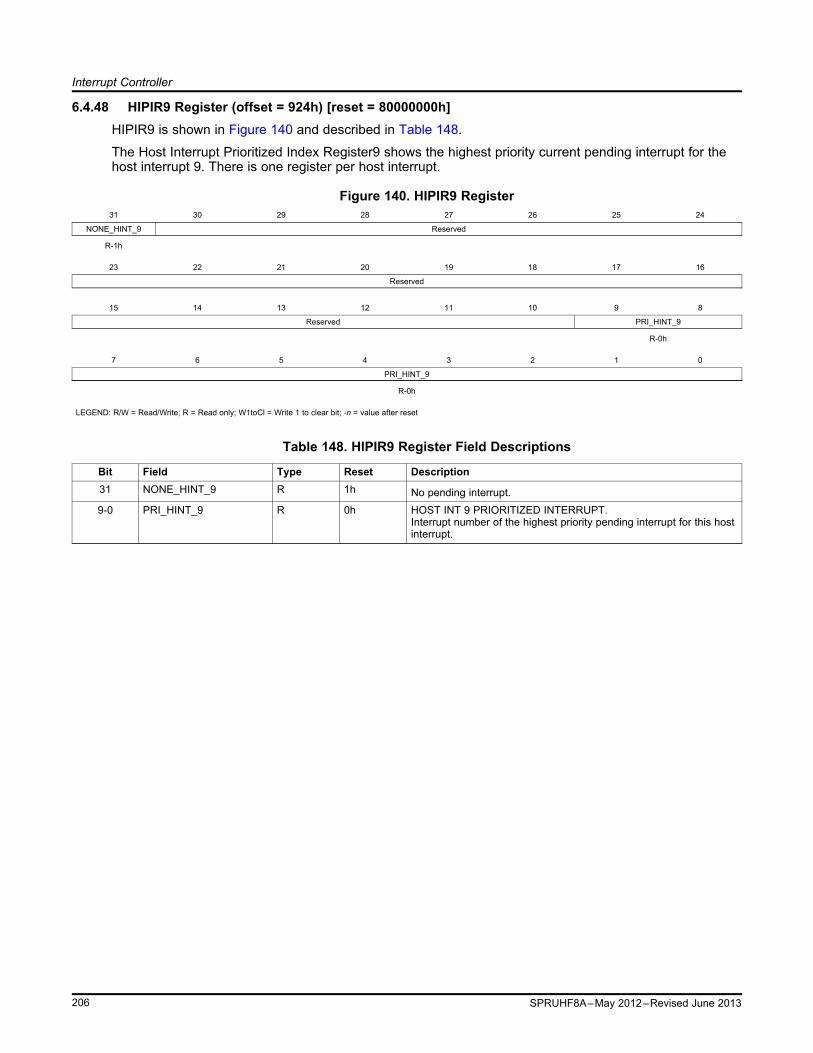
Interrupt Controller
6.4.48 HIPIR9 Register (offset = 924h) [reset = 80000000h]HIPIR9 is shown in Figure 140 and described in Table 148.
The Host Interrupt Prioritized Index Register9 shows the highest priority current pending interrupt for thehost interrupt 9. There is one register per host interrupt.
Figure 140. HIPIR9 Register31 30 29 28 27 26 25 24
NONE_HINT_9 Reserved
R-1h
23 22 21 20 19 18 17 16
Reserved
15 14 13 12 11 10 9 8
Reserved PRI_HINT_9
R-0h
7 6 5 4 3 2 1 0
PRI_HINT_9
R-0h
LEGEND: R/W = Read/Write; R = Read only; W1toCl = Write 1 to clear bit; -n = value after reset
Table 148. HIPIR9 Register Field Descriptions
Bit Field Type Reset Description31 NONE_HINT_9 R 1h No pending interrupt.9-0 PRI_HINT_9 R 0h HOST INT 9 PRIORITIZED INTERRUPT.
Interrupt number of the highest priority pending interrupt for this hostinterrupt.
206 SPRUHF8A–May 2012–Revised June 2013

Interrupt Controller
6.4.49 SIPR0 Register (offset = D00h) [reset = 1h]SIPR0 is shown in Figure 141 and described in Table 149.
The System Interrupt Polarity Register0 define the polarity of the system interrupts 0 to 31. There is apolarity for each system interrupt. The polarity of all system interrupts is active high; always write 1 to thebits of this register.
Figure 141. SIPR0 Register31 30 29 28 27 26 25 24 23 22 21 20 19 18 17 16 15 14 13 12 11 10 9 8 7 6 5 4 3 2 1 0
POLARITY_31_0
R/W-1h
LEGEND: R/W = Read/Write; R = Read only; W1toCl = Write 1 to clear bit; -n = value after reset
Table 149. SIPR0 Register Field Descriptions
Bit Field Type Reset Description31-0 POLARITY_31_0 R/W 1h Interrupt polarity of the system interrupts 0 to 31.
0 = active low.1 = active high.
207SPRUHF8A–May 2012–Revised June 2013

Interrupt Controller
6.4.50 SIPR1 Register (offset = D04h) [reset = 1h]SIPR1 is shown in Figure 142 and described in Table 150.
The System Interrupt Polarity Register1 define the polarity of the system interrupts 32 to 63. There is apolarity for each system interrupt. The polarity of all system interrupts is active high; always write 1 to thebits of this register.
Figure 142. SIPR1 Register31 30 29 28 27 26 25 24 23 22 21 20 19 18 17 16 15 14 13 12 11 10 9 8 7 6 5 4 3 2 1 0
POLARITY_63_32
R/W-1h
LEGEND: R/W = Read/Write; R = Read only; W1toCl = Write 1 to clear bit; -n = value after reset
Table 150. SIPR1 Register Field Descriptions
Bit Field Type Reset Description31-0 POLARITY_63_32 R/W 1h Interrupt polarity of the system interrupts 32 to 63.
0 = active low.1 = active high.
208 SPRUHF8A–May 2012–Revised June 2013

Interrupt Controller
6.4.51 SITR0 Register (offset = D80h) [reset = 0h]SITR0 is shown in Figure 143 and described in Table 151.
The System Interrupt Type Register0 define the type of the system interrupts 0 to 31. There is a type foreach system interrupt. The type of all system interrupts is pulse; always write 0 to the bits of this register.
Figure 143. SITR0 Register31 30 29 28 27 26 25 24 23 22 21 20 19 18 17 16 15 14 13 12 11 10 9 8 7 6 5 4 3 2 1 0
TYPE_31_0
R/W-0h
LEGEND: R/W = Read/Write; R = Read only; W1toCl = Write 1 to clear bit; -n = value after reset
Table 151. SITR0 Register Field Descriptions
Bit Field Type Reset Description31-0 TYPE_31_0 R/W 0h Interrupt type of the system interrupts 0 to 31.
0 = level or pulse interrupt.1 = edge interrupt (required edge detect).
209SPRUHF8A–May 2012–Revised June 2013

Interrupt Controller
6.4.52 SITR1 Register (offset = D84h) [reset = 0h]SITR1 is shown in Figure 144 and described in Table 152.
The System Interrupt Type Register1 define the type of the system interrupts 32 to 63. There is a type foreach system interrupt. The type of all system interrupts is pulse; always write 0 to the bits of this register.
Figure 144. SITR1 Register31 30 29 28 27 26 25 24 23 22 21 20 19 18 17 16 15 14 13 12 11 10 9 8 7 6 5 4 3 2 1 0
TYPE_63_32
R/W-0h
LEGEND: R/W = Read/Write; R = Read only; W1toCl = Write 1 to clear bit; -n = value after reset
Table 152. SITR1 Register Field Descriptions
Bit Field Type Reset Description31-0 TYPE_63_32 R/W 0h Interrupt type of the system interrupts 32 to 63.
0 = level or pulse interrupt.1 = edge interrupt (required edge detect).
210 SPRUHF8A–May 2012–Revised June 2013

Interrupt Controller
6.4.53 HINLR0 Register (offset = 1100h) [reset = 100h]HINLR0 is shown in Figure 145 and described in Table 153.
The Host Interrupt Nesting Level Register0 display and control the nesting level for host interrupt 0. Thenesting level controls which channel and lower priority channels are nested. There is one register per hostinterrupt.
Figure 145. HINLR0 Register31 30 29 28 27 26 25 24
AUTO_OVERRIDE Reserved
W-0h
23 22 21 20 19 18 17 16
Reserved
15 14 13 12 11 10 9 8
Reserved NEST_HINT_0
R/W-100h
7 6 5 4 3 2 1 0
NEST_HINT_0
R/W-100h
LEGEND: R/W = Read/Write; R = Read only; W1toCl = Write 1 to clear bit; -n = value after reset
Table 153. HINLR0 Register Field Descriptions
Bit Field Type Reset Description31 AUTO_OVERRIDE W 0h Reads return 0.
Writes of a 1 override the auto updating of the nesting_level and usethe write data.
8-0 NEST_HINT_0 R/W 100h Reads return the current nesting level for the host interrupt.Writes set the nesting level for the host interrupt.In auto mode the value is updated internally unless theauto_override is set and then the write data is used.
211SPRUHF8A–May 2012–Revised June 2013
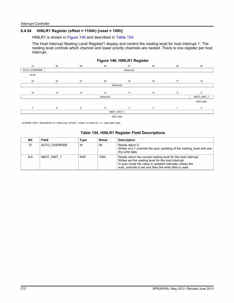
Interrupt Controller
6.4.54 HINLR1 Register (offset = 1104h) [reset = 100h]HINLR1 is shown in Figure 146 and described in Table 154.
The Host Interrupt Nesting Level Register1 display and control the nesting level for host interrupt 1. Thenesting level controls which channel and lower priority channels are nested. There is one register per hostinterrupt.
Figure 146. HINLR1 Register31 30 29 28 27 26 25 24
AUTO_OVERRIDE Reserved
W-0h
23 22 21 20 19 18 17 16
Reserved
15 14 13 12 11 10 9 8
Reserved NEST_HINT_1
R/W-100h
7 6 5 4 3 2 1 0
NEST_HINT_1
R/W-100h
LEGEND: R/W = Read/Write; R = Read only; W1toCl = Write 1 to clear bit; -n = value after reset
Table 154. HINLR1 Register Field Descriptions
Bit Field Type Reset Description31 AUTO_OVERRIDE W 0h Reads return 0.
Writes of a 1 override the auto updating of the nesting_level and usethe write data.
8-0 NEST_HINT_1 R/W 100h Reads return the current nesting level for the host interrupt.Writes set the nesting level for the host interrupt.In auto mode the value is updated internally unless theauto_override is set and then the write data is used.
212 SPRUHF8A–May 2012–Revised June 2013

Interrupt Controller
6.4.55 HINLR2 Register (offset = 1108h) [reset = 100h]HINLR2 is shown in Figure 147 and described in Table 155.
The Host Interrupt Nesting Level Register2 display and control the nesting level for host interrupt 2. Thenesting level controls which channel and lower priority channels are nested. There is one register per hostinterrupt.
Figure 147. HINLR2 Register31 30 29 28 27 26 25 24
AUTO_OVERRIDE Reserved
W-0h
23 22 21 20 19 18 17 16
Reserved
15 14 13 12 11 10 9 8
Reserved NEST_HINT_2
R/W-100h
7 6 5 4 3 2 1 0
NEST_HINT_2
R/W-100h
LEGEND: R/W = Read/Write; R = Read only; W1toCl = Write 1 to clear bit; -n = value after reset
Table 155. HINLR2 Register Field Descriptions
Bit Field Type Reset Description31 AUTO_OVERRIDE W 0h Reads return 0.
Writes of a 1 override the auto updating of the nesting_level and usethe write data.
8-0 NEST_HINT_2 R/W 100h Reads return the current nesting level for the host interrupt.Writes set the nesting level for the host interrupt.In auto mode the value is updated internally unless theauto_override is set and then the write data is used.
213SPRUHF8A–May 2012–Revised June 2013

Interrupt Controller
6.4.56 HINLR3 Register (offset = 110Ch) [reset = 100h]HINLR3 is shown in Figure 148 and described in Table 156.
The Host Interrupt Nesting Level Register3 display and control the nesting level for host interrupt 3. Thenesting level controls which channel and lower priority channels are nested. There is one register per hostinterrupt.
Figure 148. HINLR3 Register31 30 29 28 27 26 25 24
AUTO_OVERRIDE Reserved
W-0h
23 22 21 20 19 18 17 16
Reserved
15 14 13 12 11 10 9 8
Reserved NEST_HINT_3
R/W-100h
7 6 5 4 3 2 1 0
NEST_HINT_3
R/W-100h
LEGEND: R/W = Read/Write; R = Read only; W1toCl = Write 1 to clear bit; -n = value after reset
Table 156. HINLR3 Register Field Descriptions
Bit Field Type Reset Description31 AUTO_OVERRIDE W 0h Reads return 0.
Writes of a 1 override the auto updating of the nesting_level and usethe write data.
8-0 NEST_HINT_3 R/W 100h Reads return the current nesting level for the host interrupt.Writes set the nesting level for the host interrupt.In auto mode the value is updated internally unless theauto_override is set and then the write data is used.
214 SPRUHF8A–May 2012–Revised June 2013

Interrupt Controller
6.4.57 HINLR4 Register (offset = 1110h) [reset = 100h]HINLR4 is shown in Figure 149 and described in Table 157.
The Host Interrupt Nesting Level Register4 display and control the nesting level for host interrupt 4. Thenesting level controls which channel and lower priority channels are nested. There is one register per hostinterrupt.
Figure 149. HINLR4 Register31 30 29 28 27 26 25 24
AUTO_OVERRIDE Reserved
W-0h
23 22 21 20 19 18 17 16
Reserved
15 14 13 12 11 10 9 8
Reserved NEST_HINT_4
R/W-100h
7 6 5 4 3 2 1 0
NEST_HINT_4
R/W-100h
LEGEND: R/W = Read/Write; R = Read only; W1toCl = Write 1 to clear bit; -n = value after reset
Table 157. HINLR4 Register Field Descriptions
Bit Field Type Reset Description31 AUTO_OVERRIDE W 0h Reads return 0.
Writes of a 1 override the auto updating of the nesting_level and usethe write data.
8-0 NEST_HINT_4 R/W 100h Reads return the current nesting level for the host interrupt.Writes set the nesting level for the host interrupt.In auto mode the value is updated internally unless theauto_override is set and then the write data is used.
215SPRUHF8A–May 2012–Revised June 2013

Interrupt Controller
6.4.58 HINLR5 Register (offset = 1114h) [reset = 100h]HINLR5 is shown in Figure 150 and described in Table 158.
The Host Interrupt Nesting Level Register5 display and control the nesting level for host interrupt 5. Thenesting level controls which channel and lower priority channels are nested. There is one register per hostinterrupt.
Figure 150. HINLR5 Register31 30 29 28 27 26 25 24
AUTO_OVERRIDE Reserved
W-0h
23 22 21 20 19 18 17 16
Reserved
15 14 13 12 11 10 9 8
Reserved NEST_HINT_5
R/W-100h
7 6 5 4 3 2 1 0
NEST_HINT_5
R/W-100h
LEGEND: R/W = Read/Write; R = Read only; W1toCl = Write 1 to clear bit; -n = value after reset
Table 158. HINLR5 Register Field Descriptions
Bit Field Type Reset Description31 AUTO_OVERRIDE W 0h Reads return 0.
Writes of a 1 override the auto updating of the nesting_level and usethe write data.
8-0 NEST_HINT_5 R/W 100h Reads return the current nesting level for the host interrupt.Writes set the nesting level for the host interrupt.In auto mode the value is updated internally unless theauto_override is set and then the write data is used.
216 SPRUHF8A–May 2012–Revised June 2013

Interrupt Controller
6.4.59 HINLR6 Register (offset = 1118h) [reset = 100h]HINLR6 is shown in Figure 151 and described in Table 159.
The Host Interrupt Nesting Level Register6 display and control the nesting level for host interrupt 6. Thenesting level controls which channel and lower priority channels are nested. There is one register per hostinterrupt.
Figure 151. HINLR6 Register31 30 29 28 27 26 25 24
AUTO_OVERRIDE Reserved
W-0h
23 22 21 20 19 18 17 16
Reserved
15 14 13 12 11 10 9 8
Reserved NEST_HINT_6
R/W-100h
7 6 5 4 3 2 1 0
NEST_HINT_6
R/W-100h
LEGEND: R/W = Read/Write; R = Read only; W1toCl = Write 1 to clear bit; -n = value after reset
Table 159. HINLR6 Register Field Descriptions
Bit Field Type Reset Description31 AUTO_OVERRIDE W 0h Reads return 0.
Writes of a 1 override the auto updating of the nesting_level and usethe write data.
8-0 NEST_HINT_6 R/W 100h Reads return the current nesting level for the host interrupt.Writes set the nesting level for the host interrupt.In auto mode the value is updated internally unless theauto_override is set and then the write data is used.
217SPRUHF8A–May 2012–Revised June 2013

Interrupt Controller
6.4.60 HINLR7 Register (offset = 111Ch) [reset = 100h]HINLR7 is shown in Figure 152 and described in Table 160.
The Host Interrupt Nesting Level Register7 display and control the nesting level for host interrupt 7. Thenesting level controls which channel and lower priority channels are nested. There is one register per hostinterrupt.
Figure 152. HINLR7 Register31 30 29 28 27 26 25 24
AUTO_OVERRIDE Reserved
W-0h
23 22 21 20 19 18 17 16
Reserved
15 14 13 12 11 10 9 8
Reserved NEST_HINT_7
R/W-100h
7 6 5 4 3 2 1 0
NEST_HINT_7
R/W-100h
LEGEND: R/W = Read/Write; R = Read only; W1toCl = Write 1 to clear bit; -n = value after reset
Table 160. HINLR7 Register Field Descriptions
Bit Field Type Reset Description31 AUTO_OVERRIDE W 0h Reads return 0.
Writes of a 1 override the auto updating of the nesting_level and usethe write data.
8-0 NEST_HINT_7 R/W 100h Reads return the current nesting level for the host interrupt.Writes set the nesting level for the host interrupt.In auto mode the value is updated internally unless theauto_override is set and then the write data is used.
218 SPRUHF8A–May 2012–Revised June 2013

Interrupt Controller
6.4.61 HINLR8 Register (offset = 1120h) [reset = 100h]HINLR8 is shown in Figure 153 and described in Table 161.
The Host Interrupt Nesting Level Register8 display and control the nesting level for host interrupt 8. Thenesting level controls which channel and lower priority channels are nested. There is one register per hostinterrupt.
Figure 153. HINLR8 Register31 30 29 28 27 26 25 24
AUTO_OVERRIDE Reserved
W-0h
23 22 21 20 19 18 17 16
Reserved
15 14 13 12 11 10 9 8
Reserved NEST_HINT_8
R/W-100h
7 6 5 4 3 2 1 0
NEST_HINT_8
R/W-100h
LEGEND: R/W = Read/Write; R = Read only; W1toCl = Write 1 to clear bit; -n = value after reset
Table 161. HINLR8 Register Field Descriptions
Bit Field Type Reset Description31 AUTO_OVERRIDE W 0h Reads return 0.
Writes of a 1 override the auto updating of the nesting_level and usethe write data.
8-0 NEST_HINT_8 R/W 100h Reads return the current nesting level for the host interrupt.Writes set the nesting level for the host interrupt.In auto mode the value is updated internally unless theauto_override is set and then the write data is used.
219SPRUHF8A–May 2012–Revised June 2013
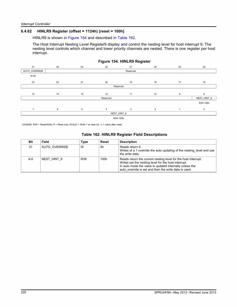
Interrupt Controller
6.4.62 HINLR9 Register (offset = 1124h) [reset = 100h]HINLR9 is shown in Figure 154 and described in Table 162.
The Host Interrupt Nesting Level Register9 display and control the nesting level for host interrupt 9. Thenesting level controls which channel and lower priority channels are nested. There is one register per hostinterrupt.
Figure 154. HINLR9 Register31 30 29 28 27 26 25 24
AUTO_OVERRIDE Reserved
W-0h
23 22 21 20 19 18 17 16
Reserved
15 14 13 12 11 10 9 8
Reserved NEST_HINT_9
R/W-100h
7 6 5 4 3 2 1 0
NEST_HINT_9
R/W-100h
LEGEND: R/W = Read/Write; R = Read only; W1toCl = Write 1 to clear bit; -n = value after reset
Table 162. HINLR9 Register Field Descriptions
Bit Field Type Reset Description31 AUTO_OVERRIDE W 0h Reads return 0.
Writes of a 1 override the auto updating of the nesting_level and usethe write data.
8-0 NEST_HINT_9 R/W 100h Reads return the current nesting level for the host interrupt.Writes set the nesting level for the host interrupt.In auto mode the value is updated internally unless theauto_override is set and then the write data is used.
220 SPRUHF8A–May 2012–Revised June 2013

Interrupt Controller
6.4.63 HIER Register (offset = 1500h) [reset = 0h]HIER is shown in Figure 155 and described in Table 163.
The Host Interrupt Enable Registers enable or disable individual host interrupts. These work separatelyfrom the global enables. There is one bit per host interrupt. These bits are updated when writing to theHost Interrupt Enable Index Set and Host Interrupt Enable Index Clear registers.
Figure 155. HIER Register31 30 29 28 27 26 25 24 23 22 21 20 19 18 17 16 15 14 13 12 11 10 9 8 7 6 5 4 3 2 1 0
Reserved ENABLE_HINT
R/W-0h
LEGEND: R/W = Read/Write; R = Read only; W1toCl = Write 1 to clear bit; -n = value after reset
Table 163. HIER Register Field Descriptions
Bit Field Type Reset Description9-0 ENABLE_HINT R/W 0h The enable of the host interrupts (one per bit).
0 = disabled1 = enabled
221SPRUHF8A–May 2012–Revised June 2013

PRU-ICSS Interrupts
7 PRU-ICSS Interrupts
Table 164. PRU-ICSS InterruptsInt Number Signal Name (Non-Ethercat Source Signal Name
Mode) (Ethercat Mode) (1)
63 tpcc_int_pend_po1 TPCC (EDMA)62 tpcc_errint_pend_po TPCC (EDMA)61 tptc_erint_pend_po TPTC0 (EDMA)60 initiator_sinterrupt_q_n1 Mbox0 - mail_u1_irq (mailbox
interrupt for pru0)59 initiator_sinterrupt_q_n2 Mbox0 - mail_u2_irq (mailbox
interrupt for pru1)58 Emulation Suspend Signal Debugss
(software use)57 POINTRPEND1 GPIO056 pwm_trip_zone eHRPWM0/eHRPWM1/eHRP
WM255 mcasp_x_intr_pend McASP0 Tx pr1_mii1_crs(external)54 mcasp_r_intr_pend McASP0 Rx PRU1_RX_EOF53 gen_intr_pend ADC_TSC MDIO_MII_LINK[1]52 nirq UART2 PORT1_TX_OVERFLOW51 nirq UART0 PORT1_TX_UNDERFLOW50 c0_rx_thresh_pend 3PGSW (GEMAC) PRU1_RX_OVERFLOW49 c0_rx_pend 3PGSW (GEMAC) PRU1_RX_NIBBLE_ODD48 c0_tx_pend 3PGSW (GEMAC) PRU1_RX_CRC47 c0_misc_pend 3PGSW (GEMAC) PRU1_RX_SOF46 epwm_intr_intr_pend eHRPWM1 PRU1_RX_SFD45 eqep_intr_intr_pend eQEP0 PRU1_RX_ERR3244 SINTERRUPTN McSPI0 PRU1_RX_ERR43 epwm_intr_intr_pend eHRPWM0 pr1_mii0_crs(external)42 ecap_intr_intr_pend eCAP0 PRU0_RX_EOF41 POINTRPEND I2C0 MDIO_MII_LINK[0]40 dcan_intr DCAN0 PORT0_TX_OVERFLOW39 dcan_int1 DCAN0 PORT0_TX_UNDERFLOW38 dcan_uerr DCAN0 PRU0_RX_OVERFLOW37 epwm_intr_intr_pend eHRPWM2 PRU0_RX_NIBBLE_ODD36 ecap_intr_intr_pend eCAP2 PRU0_RX_CRC35 ecap_intr_intr_pend eCAP1 PRU0_RX_SOF34 mcasp_r_intr_pend McASP1 Rx PRU0_RX_SFD33 mcasp_x_intr_pend McASP1 Tx PRU0_RX_ERR3232 nirq UART1 PRU0_RX_ERR31 pr1_pru_mst_intr[15]_intr_req pru0 or pru130 pr1_pru_mst_intr[14]_intr_req pru0 or pru129 pr1_pru_mst_intr[13]_intr_req pru0 or pru128 pr1_pru_mst_intr[12]_intr_req pru0 or pru127 pr1_pru_mst_intr[11]_intr_req pru0 or pru1 PRU-ICSS Internal Interrupts26 pr1_pru_mst_intr[10]_intr_req pru0 or pru125 pr1_pru_mst_intr[9]_intr_req pru0 or pru124 pr1_pru_mst_intr[8]_intr_req pru0 or pru123 pr1_pru_mst_intr[7]_intr_req pru0 or pru1
(1) Signals 63–56 and 31–0 for Ethercat Mode are the same as for Non-Ethercat Mode.
22 SPRUHF8A–May 2012–Revised June 2013

PRU-ICSS Interrupts
Table 164. PRU-ICSS Interrupts (continued)Int Number Signal Name (Non-Ethercat Source Signal Name
Mode) (Ethercat Mode) (1)
22 pr1_pru_mst_intr[6]_intr_req pru0 or pru121 pr1_pru_mst_intr[5]_intr_req pru0 or pru120 pr1_pru_mst_intr[4]_intr_req pru0 or pru119 pr1_pru_mst_intr[3]_intr_req pru0 or pru118 pr1_pru_mst_intr[2]_intr_req pru0 or pru117 pr1_pru_mst_intr[1]_intr_req pru0 or pru116 pr1_pru_mst_intr[0]_intr_req pru0 or pru115 pr1_ecap_intr_req PRU-ICSS eCAP14 sync0_out_pend PRU-ICSS IEP (Ethercat)13 sync1_out_pend PRU-ICSS IEP (Ethercat)12 latch0_in (input to PRU-ICSS) PRU-ICSS IEP (Ethercat) PRU-ICSS Internal Interrupts11 latch1_in (input to PRU-ICSS) PRU-ICSS IEP (Ethercat)10 pdi_wd_exp_pend PRU-ICSS IEP (Ethercat)9 pd_wd_exp_pend PRU-ICSS IEP (Ethercat)8 digio_event_req PRU-ICSS IEP (Ethercat)7 pr1_iep_tim_cap_cmp_pend PRU-ICSS IEP6 pr1_uart_uint_intr_req PRU-ICSS UART5 pr1_uart_utxevt_intr_req PRU-ICSS UART4 pr1_uart_urxevt_intr_req PRU-ICSS UART3 pr1_xfr_timeout PRU-ICSS Scratch Pad2 pr1_pru1_r31_status_cnt16 PRU1 (Shift Capture)1 pr1_pru0_r31_status_cnt16 PRU0 (Shift Capture)0 pr1_parity_err_intr_pend PRU-ICSS Parity Logic
Note: For the availability of EtherCAT and non-EtherCAT mode, see Chapter 1, Introduction, in theAM335x ARM® Cortex™-A8 Microprocessors (MPUs) Technical Reference Manual (literature numberSPRUH73).
223SPRUHF8A–May 2012–Revised June 2013

Universal Asynchronous Receiver/Transmitter
8 Universal Asynchronous Receiver/Transmitter
8.1 Introduction
8.1.1 Purpose of the PeripheralThe UART peripheral is based on the industry standard TL16C550 asynchronous communicationselement, which in turn is a functional upgrade of the TL16C450. Functionally similar to the TL16C450 onpower up (single character or TL16C450 mode), the UART can be placed in an alternate FIFO(TL16C550) mode. This relieves the CPU of excessive software overhead by buffering received andtransmitted characters. The receiver and transmitter FIFOs store up to 16 bytes including three additionalbits of error status per byte for the receiver FIFO.
The UART performs serial-to-parallel conversions on data received from a peripheral device and parallel-to-serial conversion on data received from the CPU. The CPU can read the UART status at any time. TheUART includes control capability and a processor interrupt system that can be tailored to minimizesoftware management of the communications link.
The UART includes a programmable baud generator capable of dividing the UART input clock by divisorsfrom 1 to 65535 and producing a 16× reference clock or a 13× reference clock for the internal transmitterand receiver logic. For detailed timing and electrical specifications for the UART, see your device-specificdata manual.
8.1.2 FeaturesCheck your device-specific data manual to see the list of features that are supported and that are notsupported by the UART.
8.1.3 Functional Block DiagramA functional block diagram of the UART is shown in Figure 156.
8.1.4 Industry Standard(s) Compliance StatementThe UART peripheral is based on the industry standard TL16C550 asynchronous communicationselement, which is a functional upgrade of the TL16C450. The information in this chapter assumes you arefamiliar with these standards.
224 SPRUHF8A–May 2012–Revised June 2013

8
ReceiverBuffer
Register
DivisorLatch (LS)
DivisorLatch (MS)
BaudGenerator
ReceiverFIFO
LineStatus
Register
TransmitterHoldingRegister
Modem
Control
Register
LineControlRegister
TransmitterFIFO
InterruptEnable
Register
InterruptIdentification
Register
FIFOControlRegister
Interrupt/Event
ControlLogic
Select
DataBus
Buffer
UARTn_RXD
UARTn_TXD
PeripheralBus
Select
ReceiverShift
Register
ReceiverTiming and
Control
TransmitterTiming and
Control
TransmitterShift
Register
Control
Logic
16
8
8
8
8
8
Interrupt to CPU
16
8
signal
signal
8
88
8
Power andEmulation
ControlRegister
Event to DMA controller
Universal Asynchronous Receiver/Transmitter
Figure 156. UART Block Diagram
NOTE: The value n indicates the applicable UART where there are multiple instances. For the PRU-ICSS, there isonly one instance and all UART signals should reflect this (e.g., UART0_TXD instead of UARTn_TXD).
225SPRUHF8A–May 2012–Revised June 2013

PRU-ICSS
generator
Clock
DLH:DLL
UART input clockInput clock
UART
Receiver
timing and
control
Transmitter
timing and
control
Baud
generator
BCLK
Other logic
UART input clock frequencyDivisor MDR.OSM _ SEL 1
Desired baud rate 13= =é ùë û´
UART input clock frequencyDivisor MDR.OSM _ SEL 0
Desired baud rate 16= =é ùë û´
Universal Asynchronous Receiver/Transmitter
8.2 Functional Description
8.2.1 Clock Generation and ControlThe UART bit clock is derived from an input clock to the UART. See your device-specific data manual tocheck the maximum data rate supported by the UART.
Figure 157 is a conceptual clock generation diagram for the UART. The processor clock generatorreceives a signal from an external clock source and produces a UART input clock with a programmedfrequency. The UART contains a programmable baud generator that takes an input clock and divides it bya divisor in the range between 1 and (216 - 1) to produce a baud clock (BCLK). The frequency of BCLK issixteen times (16×) the baud rate (each received or transmitted bit lasts 16 BCLK cycles) or thirteen times(13×) the baud rate (each received or transmitted bit lasts 13 BCLK cycles). When the UART is receiving,the bit is sampled in the 8th BCLK cycle for 16× over sampling mode and on the 6th BCLK cycle for 13×over-sampling mode. The 16× or 13× reference clock is selected by configuring the OSM_SEL bit in themode definition register (MDR). The formula to calculate the divisor is:
Two 8-bit register fields (DLH and DLL), called divisor latches, hold this 16-bit divisor. DLH holds the mostsignificant bits of the divisor, and DLL holds the least significant bits of the divisor. For information aboutthese register fields, see the UART register descriptions. These divisor latches must be loaded duringinitialization of the UART in order to ensure desired operation of the baud generator. Writing to the divisorlatches results in two wait states being inserted during the write access while the baud generator is loadedwith the new value.
Figure 158 summarizes the relationship between the transferred data bit, BCLK, and the UART inputclock. Note that the timing relationship depicted in Figure 158 shows that each bit lasts for 16 BCLKcycles . This is in case of 16x over-sampling mode. For 13× over-sampling mode each bit lasts for 13BCLK cycles .
Example baud rates and divisor values relative to a 150-MHz UART input clock and 16× over-samplingmode are shown in Table 165.
Figure 157. UART Clock Generation Diagram
2 SPRUHF8A–May 2012–Revised June 2013

BCLK
Each bit lasts 16 BCLK cycles.When receiving, the UART samples the bit in the 8th cycle.
D0
UARTn_TXD,UARTn_RXD D1 D2
PARITYD7D6D5 STOP2STOP1D1 D4D2 D3START D0UARTn_TXD,UARTn_RXD
UART input clock
n UART input clock cycles, where n = divisor in DLH:DLL
n
BCLK
Universal Asynchronous Receiver/Transmitter
Figure 158. Relationships Between Data Bit, BCLK, and UART Input Clock
Table 165. Baud Rate Examples for 150-MHZ UART Input Clock and 16× Over-sampling ModeBaud Rate Divisor Value Actual Baud Rate Error (%)2400 3906 2400.154 0.014800 1953 4800.372 0.019600 977 9595.701 -0.0419200 488 19211.066 0.0638400 244 38422.131 0.0656000 167 56137.725 0.25128000 73 129807.7 0.333000000 3 3125000 4.00
Table 166. Baud Rate Examples for 150-MHZ UART Input Clock and 13× Over-sampling ModeBaud Rate Divisor Value Actual Baud Rate Error (%)2400 4808 2399 -0.014800 2404 4799.646 -0.019600 1202 9599.386 -0.0119200 601 19198.771 -0.0138400 300 38461.538 0.1656000 206 56011.949 0.02128000 90 128205.128 0.163000000 4 2884615.385 -4.00
227SPRUHF8A–May 2012–Revised June 2013

Universal Asynchronous Receiver/Transmitter
8.2.2 Signal DescriptionsThe UARTs utilize a minimal number of signal connections to interface with external devices. The UARTsignal descriptions are included in Table 167. Note that the number of UARTs and their supportedfeatures vary on each device, see your device-specific data manual for more details.
Table 167. UART Signal Descriptions
Signal Name (1) Signal Type FunctionUARTn_TXD Output Serial data transmitUARTn_RXD Input Serial data receiveUARTn_CTS (2) Input Clear-to-Send handshaking signalUARTn_RTS (2) Output Request-to-Send handshaking signal
(1) The value n indicates the applicable UART; that is, UART0, UART1, etc.(2) This signal is not supported in all UARTs. See your device-specific data manual to check if it is
supported.
8.2.3 Pin MultiplexingExtensive pin multiplexing is used to accommodate the largest number of peripheral functions in thesmallest possible package. Pin multiplexing is controlled using a combination of hardware configuration atdevice reset and software programmable register settings. See your device-specific data manual todetermine how pin multiplexing affects the UART.
8.2.4 Protocol Description
8.2.4.1 Transmission
The UART transmitter section includes a transmitter hold register (THR) and a transmitter shift register(TSR). When the UART is in the FIFO mode, THR is a 16-byte FIFO. Transmitter section control is afunction of the UART line control register (LCR). Based on the settings chosen in LCR, the UARTtransmitter sends the following to the receiving device:• 1 START bit• 5, 6, 7, or 8 data bits• 1 PARITY bit (optional)• 1, 1.5, or 2 STOP bits
8.2.4.2 Reception
The UART receiver section includes a receiver shift register (RSR) and a receiver buffer register (RBR).When the UART is in the FIFO mode, RBR is a 16-byte FIFO. Receiver section control is a function of theUART line control register (LCR). Based on the settings chosen in LCR, the UART receiver accepts thefollowing from the transmitting device:• 1 START bit• 5, 6, 7, or 8 data bits• 1 PARITY bit (optional)• 1 STOP bit (any other STOP bits transferred with the above data are not detected)
228 SPRUHF8A–May 2012–Revised June 2013

Universal Asynchronous Receiver/Transmitter
8.2.4.3 Data Format
The UART transmits in the following format:
1 START bit + data bits (5, 6, 7, 8) + 1 PARITY bit (optional) + STOP bit (1, 1.5, 2)
It transmits 1 START bit; 5, 6, 7, or 8 data bits, depending on the data width selection; 1 PARITY bit, ifparity is selected; and 1, 1.5, or 2 STOP bits, depending on the STOP bit selection.
The UART receives in the following format:
1 START bit + data bits (5, 6, 7, 8) + 1 PARITY bit (optional) + 1 STOP bit
It receives 1 START bit; 5, 6, 7, or 8 data bits, depending on the data width selection; 1 PARITY bit, ifparity is selected; and 1 STOP bit.
The protocol formats are shown in Figure 159.
Figure 159. UART Protocol FormatsTransmit/Receive for 5-bit data, parity Enable, 1 STOP bit
D0 D1 D2 D3 D4 PARITY STOP1
Transmit/Receive for 6-bit data, parity Enable, 1 STOP bit
D0 D1 D2 D3 D4 D5 PARITY STOP1
Transmit/Receive for 7-bit data, parity Enable, 1 STOP bit
D0 D1 D2 D3 D4 D5 D6 PARITY STOP1
Transmit/Receive for 8-bit data, parity Enable, 1 STOP bit
D0 D1 D2 D3 D4 D5 D6 D7 PARITY STOP1
229SPRUHF8A–May 2012–Revised June 2013

Universal Asynchronous Receiver/Transmitter
8.2.5 Operation
8.2.5.1 Transmission
The UART transmitter section includes a transmitter hold register (THR) and a transmitter shift register(TSR). When the UART is in the FIFO mode, THR is a 16-byte FIFO. Transmitter section control is afunction of the UART line control register (LCR). Based on the settings chosen in LCR, the UARTtransmitter sends the following to the receiving device:• 1 START bit• 5, 6, 7, or 8 data bits• 1 PARITY bit (optional)• 1, 1.5, or 2 STOP bits
THR receives data from the internal data bus, and when TSR is ready, the UART moves the data fromTHR to TSR. The UART serializes the data in TSR and transmits the data on the UARTn_TXD pin.
In the non-FIFO mode, if THR is empty and the THR empty (THRE) interrupt is enabled in the interruptenable register (IER), an interrupt is generated. This interrupt is cleared when a character is loaded intoTHR or the interrupt identification register (IIR) is read. In the FIFO mode, the interrupt is generated whenthe transmitter FIFO is empty, and it is cleared when at least one byte is loaded into the FIFO or IIR isread.
8.2.5.2 Reception
The UART receiver section includes a receiver shift register (RSR) and a receiver buffer register (RBR).When the UART is in the FIFO mode, RBR is a 16-byte FIFO. Timing is supplied by the 16× receiverclock. Receiver section control is a function of the UART line control register (LCR). Based on the settingschosen in LCR, the UART receiver accepts the following from the transmitting device:• 1 START bit• 5, 6, 7, or 8 data bits• 1 PARITY bit (optional)• 1 STOP bit (any other STOP bits transferred with the above data are not detected)
RSR receives the data bits from the UARTn_RXD pin. Then RSR concatenates the data bits and movesthe resulting value into RBR (or the receiver FIFO). The UART also stores three bits of error statusinformation next to each received character, to record a parity error, framing error, or break.
In the non-FIFO mode, when a character is placed in RBR and the receiver data-ready interrupt is enabledin the interrupt enable register (IER), an interrupt is generated. This interrupt is cleared when the characteris read from RBR. In the FIFO mode, the interrupt is generated when the FIFO is filled to the trigger levelselected in the FIFO control register (FCR), and it is cleared when the FIFO contents drop below thetrigger level.
230 SPRUHF8A–May 2012–Revised June 2013

Universal Asynchronous Receiver/Transmitter
8.2.5.3 FIFO Modes
The following two modes can be used for servicing the receiver and transmitter FIFOs:• FIFO interrupt mode. The FIFO is enabled and the associated interrupts are enabled. Interrupts are
sent to the CPU to indicate when specific events occur.• FIFO poll mode. The FIFO is enabled but the associated interrupts are disabled. The CPU polls status
bits to detect specific events.
Because the receiver FIFO and the transmitter FIFO are controlled separately, either one or both can beplaced into the interrupt mode or the poll mode.
8.2.5.3.1 FIFO Interrupt Mode
When the receiver FIFO is enabled in the FIFO control register (FCR) and the receiver interrupts areenabled in the interrupt enable register (IER), the interrupt mode is selected for the receiver FIFO. Thefollowing are important points about the receiver interrupts:• The receiver data-ready interrupt is issued to the CPU when the FIFO has reached the trigger level
that is programmed in FCR. It is cleared when the CPU or the DMA controller reads enough charactersfrom the FIFO such that the FIFO drops below its programmed trigger level.
• The receiver line status interrupt is generated in response to an overrun error, a parity error, a framingerror, or a break. This interrupt has higher priority than the receiver data-ready interrupt. For details,see Section 8.2.8.
• The data-ready (DR) bit in the line status register (LSR) indicates the presence or absence ofcharacters in the receiver FIFO. The DR bit is set when a character is transferred from the receivershift register (RSR) to the empty receiver FIFO. The DR bit remains set until the FIFO is empty again.
• A receiver time-out interrupt occurs if all of the following conditions exist:– At least one character is in the FIFO,– The most recent character was received more than four continuous character times ago. A
character time is the time allotted for 1 START bit, n data bits, 1 PARITY bit, and 1 STOP bit,where n depends on the word length selected with the WLS bits in the line control register (LCR).See Table 168.
– The most recent read of the FIFO has occurred more than four continuous character times before.• Character times are calculated by using the baud rate.• When a receiver time-out interrupt has occurred, it is cleared and the time-out timer is cleared when
the CPU or the EDMA controller reads one character from the receiver FIFO. The interrupt is alsocleared if a new character is received in the FIFO or if the URRST bit is cleared in the power andemulation management register (PWREMU_MGMT).
• If a receiver time-out interrupt has not occurred, the time-out timer is cleared after a new character isreceived or after the CPU or EDMA reads the receiver FIFO.
When the transmitter FIFO is enabled in FCR and the transmitter holding register empty (THRE) interruptis enabled in IER, the interrupt mode is selected for the transmitter FIFO. The THRE interrupt occurs whenthe transmitter FIFO is empty. It is cleared when the transmitter hold register (THR) is loaded (1 to 16characters may be written to the transmitter FIFO while servicing this interrupt) or the interruptidentification register (IIR) is read.
Table 168. Character Time for Word Lengths
Word Length (n) Character Time Four Character Times5 Time for 8 bits Time for 32 bits6 Time for 9 bits Time for 36 bits7 Time for 10 bits Time for 40 bits8 Time for 11 bits Time for 44 bits
231SPRUHF8A–May 2012–Revised June 2013

rts
Receiver
FIFO
D[7:0]
UART
Serial toParallel
FlowControl
Transmitter
FIFO
Parallel toSerial
FlowControl
Parallel toSerial
FlowControl
Serial toParallel
FlowControl
UART
Transmitter
FIFO
Receiver
FIFO
D[7:0]
Device Off-chip
tx
cts
rx
UARTn_RXD
UARTn_RTS
UARTn_TXD
UARTn_CTS
Universal Asynchronous Receiver/Transmitter
8.2.5.3.2 FIFO Poll Mode
When the receiver FIFO is enabled in the FIFO control register (FCR) and the receiver interrupts aredisabled in the interrupt enable register (IER), the poll mode is selected for the receiver FIFO. Similarly,when the transmitter FIFO is enabled and the transmitter interrupts are disabled, the transmitted FIFO is inthe poll mode. In the poll mode, the CPU detects events by checking bits in the line status register (LSR):• The RXFIFOE bit indicates whether there are any errors in the receiver FIFO.• The TEMT bit indicates that both the transmitter holding register (THR) and the transmitter shift
register (TSR) are empty.• The THRE bit indicates when THR is empty.• The BI (break), FE (framing error), PE (parity error), and OE (overrun error) bits specify which error or
errors have occurred.• The DR (data-ready) bit is set as long as there is at least one byte in the receiver FIFO.
Also, in the FIFO poll mode:• The interrupt identification register (IIR) is not affected by any events because the interrupts are
disabled.• The UART does not indicate when the receiver FIFO trigger level is reached or when a receiver time-
out occurs.
8.2.5.4 Autoflow Control
The UART can employ autoflow control by connecting the UARTn_CTS and UARTn_RTS signals. Notethat all UARTs do not support autoflow control, see your device-specific data manual for supportedfeatures. The UARTn_CTS input must be active before the transmitter FIFO can transmit data. TheUARTn_RTS becomes active when the receiver needs more data and notifies the sending device. WhenUARTn_RTS is connected to UARTn_CTS, data transmission does not occur unless the receiver FIFOhas space for the data. Therefore, when two UARTs are connected as shown in Figure 160 with autoflowenabled, overrun errors are eliminated.
Figure 160. UART Interface Using Autoflow Diagram
232 SPRUHF8A–May 2012–Revised June 2013

UARTn_TXD
UARTn_CTS
Start StopBits0−7 Start StopBits 0−7 Start StopBits 0−7
UARTn_RXD
UARTn_RTS
Start Start StartStopStopBits N Bits N+1Start Stop
Universal Asynchronous Receiver/Transmitter
8.2.5.4.1 UARTn_RTS Behavior
UARTn_RTS data flow control originates in the receiver block (see Figure 156). When the receiver FIFOlevel reaches a trigger level of 1, 4, 8, or 14 (see Figure 161), UARTn_RTS is deasserted. The sendingUART may send an additional byte after the trigger level is reached (assuming the sending UART hasanother byte to send), because it may not recognize the deassertion of UARTn_RTS until after it hasbegun sending the additional byte. For trigger level 1, 4, and 8, UARTn_RTS is automatically reassertedonce the receiver FIFO is emptied. For trigger level 14, UARTn_RTS is automatically reasserted once thereceiver FIFO drops below the trigger level.
Figure 161. Autoflow Functional Timing Waveforms for UARTn_RTS
(1) N = Receiver FIFO trigger level.(2) The two blocks in dashed lines cover the case where an additional byte is sent.
8.2.5.4.2 UARTn_CTS Behavior
The transmitter checks UARTn_CTS before sending the next data byte. If UARTn_CTS is active, thetransmitter sends the next byte. To stop the transmitter from sending the following byte, UARTn_CTSmust be released before the middle of the last STOP bit that is currently being sent (see Figure 162).When flow control is enabled, UARTn_CTS level changes do not trigger interrupts because the deviceautomatically controls its own transmitter. Without autoflow control, the transmitter sends any data presentin the transmitter FIFO and a receiver overrun error may result.
Figure 162. Autoflow Functional Timing Waveforms for UARTn_CTS
(1) When UARTn_CTS is active (low), the transmitter keeps sending serial data out.(2) When UARTn_CTS goes high before the middle of the last STOP bit of the current byte, the transmitter
finishes sending the current byte but it does not send the next byte.(3) When UARTn_CTS goes from high to low, the transmitter begins sending data again.
8.2.5.5 Loopback Control
The UART can be placed in the diagnostic mode using the LOOP bit in the modem control register (MCR),which internally connects the UART output back to the UART input. In this mode, the transmit and receivedata paths, the transmitter and receiver interrupts, and the modem control interrupts can be verifiedwithout connecting to another UART.
233SPRUHF8A–May 2012–Revised June 2013
Universal Asynchronous Receiver/Transmitter
8.2.6 Reset Considerations
8.2.6.1 Software Reset Considerations
Two bits in the power and emulation management register (PWREMU_MGMT) control resetting the partsof the UART:• The UTRST bit controls resetting the transmitter only. If UTRST = 1, the transmitter is active;
if UTRST = 0, the transmitter is in reset.• The URRST bit controls resetting the receiver only. If URRST = 1, the receiver is active;
if URRST = 0, the receiver is in reset.
In each case, putting the receiver and/or transmitter in reset will reset the state machine of the affectedportion but does not affect the UART registers.
8.2.6.2 Hardware Reset Considerations
When the processor RESET pin is asserted, the entire processor is reset and is held in the reset stateuntil the RESET pin is released. As part of a device reset, the UART state machine is reset and the UARTregisters are forced to their default states. The default states of the registers are shown in .
8.2.7 InitializationThe following steps are required to initialize the UART:1. Perform the necessary device pin multiplexing setup (see your device-specific data manual).2. Set the desired baud rate by writing the appropriate clock divisor values to the divisor latch registers
(DLL and DLH).3. If the FIFOs will be used, select the desired trigger level and enable the FIFOs by writing the
appropriate values to the FIFO control register (FCR). The FIFOEN bit in FCR must be set first, beforethe other bits in FCR are configured.
4. Choose the desired protocol settings by writing the appropriate values to the line control register(LCR).
5. If autoflow control is desired, write appropriate values to the modem control register (MCR). Note thatall UARTs do not support autoflow control, see your device-specific data manual for supportedfeatures.
6. Choose the desired response to emulation suspend events by configuring the FREE bit and enable theUART by setting the UTRST and URRST bits in the power and emulation management register(PWREMU_MGMT).
8.2.8 Interrupt Support
8.2.8.1 Interrupt Events and Requests
The UART generates the interrupt requests described in Table 169. All requests are multiplexed throughan arbiter to a single UART interrupt request to the CPU, as shown in Figure 163. Each of the interruptrequests has an enable bit in the interrupt enable register (IER) and is recorded in the interruptidentification register (IIR).
If an interrupt occurs and the corresponding enable bit is set to 1, the interrupt request is recorded in IIRand is forwarded to the CPU. If an interrupt occurs and the corresponding enable bit is cleared to 0, theinterrupt request is blocked. The interrupt request is neither recorded in IIR nor forwarded to the CPU.
8.2.8.2 Interrupt Multiplexing
The UARTs have dedicated interrupt signals to the CPU and the interrupts are not multiplexed with anyother interrupt source.
234 SPRUHF8A–May 2012–Revised June 2013

UART interruptrequest to CPU
IER(ETBEI)
IER(ERBI)
Transmitter holdingregister empty
Receiver data ready
THREINT
RDRINT
Overrun error
IER(ELSI)
RTOINT
Conditions Enable bits UART interrupt requests
Arbiter
Parity errorFraming error
Break
RLSINT
Receiver time-out
Universal Asynchronous Receiver/Transmitter
Table 169. UART Interrupt Requests DescriptionsUART InterruptRequest Interrupt Source CommentTHREINT THR-empty condition: The transmitter holding register If THREINT is enabled in IER, by setting the ETBEI
(THR) or the transmitter FIFO is empty. All of the data bit, it is recorded in IIR.has been copied from THR to the transmitter shift As an alternative to using THREINT, the CPU can pollregister (TSR). the THRE bit in the line status register (LSR).
RDAINT Receive data available in non-FIFO mode or trigger If RDAINT is enabled in IER, by setting the ERBI bit,level reached in the FIFO mode. it is recorded in IIR.
As an alternative to using RDAINT, the CPU can pollthe DR bit in the line status register (LSR). In theFIFO mode, this is not a functionally equivalentalternative because the DR bit does not respond tothe FIFO trigger level. The DR bit only indicates thepresence or absence of unread characters.
RTOINT Receiver time-out condition (in the FIFO mode only): The receiver time-out interrupt prevents the UARTNo characters have been removed from or input to from waiting indefinitely, in the case when the receiverthe receiver FIFO during the last four character times FIFO level is below the trigger level and thus does not(see Table 168), and there is at least one character in generate a receiver data-ready interrupt.the receiver FIFO during this time. If RTOINT is enabled in IER, by setting the ERBI bit,
it is recorded in IIR.There is no status bit to reflect the occurrence of atime-out condition.
RLSINT Receiver line status condition: An overrun error, parity If RLSINT is enabled in IER, by setting the ELSI bit, iterror, framing error, or break has occurred. is recorded in IIR.
As an alternative to using RLSINT, the CPU can pollthe following bits in the line status register (LSR):overrun error indicator (OE), parity error indicator(PE), framing error indicator (FE), and break indicator(BI).
Figure 163. UART Interrupt Request Enable Paths
235SPRUHF8A–May 2012–Revised June 2013

Universal Asynchronous Receiver/Transmitter
8.2.9 DMA Event SupportIn the FIFO mode, the UART generates the following two DMA events:• Receive event (URXEVT): The trigger level for the receiver FIFO (1, 4, 8, or 14 characters) is set with
the RXFIFTL bit in the FIFO control register (FCR). Every time the trigger level is reached or a receivertime-out occurs, the UART sends a receive event to the EDMA controller. In response, the EDMAcontroller reads the data from the receiver FIFO by way of the receiver buffer register (RBR). Note thatthe receive event is not asserted if the data at the top of the receiver FIFO is erroneous even if thetrigger level has been reached.
• Transmit event (UTXEVT): When the transmitter FIFO is empty (when the last byte in the transmitterFIFO has been copied to the transmitter shift register), the UART sends an UTXEVT signal to theEDMA controller. In response, the EDMA controller refills the transmitter FIFO by way of the transmitterholding register (THR). The UTXEVT signal is also sent to the DMA controller when the UART is takenout of reset using the UTRST bit in the power and emulation management register(PWREMU_MGMT).
Activity in DMA channels can be synchronized to these events. In the non-FIFO mode, the UARTgenerates no DMA events. Any DMA channel synchronized to either of these events must be enabled atthe time the UART event is generated. Otherwise, the DMA channel will miss the event and, unless theUART generates a new event, no data transfer will occur.
8.2.10 Power ManagementThe UART peripheral can be placed in reduced-power modes to conserve power during periods of lowactivity. The power management of the UART peripheral is controlled by the processor Power and ClockManagement (PRCM). The PRCM acts as a master controller for power management for all of theperipherals on the device. For detailed information on power management procedures using the PSC, seethe chapter Power, Reset, and Clock Management (PRCM) in the device reference manual.
8.2.11 Emulation ConsiderationsThe FREE bit in the power and emulation management register (PWREMU_MGMT) determines how theUART responds to an emulation suspend event such as an emulator halt or breakpoint. If FREE = 0 and atransmission is in progress, the UART halts after completing the one-word transmission; if FREE = 0 anda transmission is not in progress, the UART halts immediately. If FREE = 1, the UART does not halt andcontinues operating normally.
Note also that most emulator accesses are transparent to UART operation. Emulator read operations donot affect any register contents, status bits, or operating states, with the exception of the interruptidentification register (IIR). Emulator writes, however, may affect register contents and may affect UARToperation, depending on what register is accessed and what value is written.
The UART registers can be read from or written to during emulation suspend events, even if the UARTactivity has stopped.
8.2.12 Exception Processing
8.2.12.1 Divisor Latch Not Programmed
Since the processor reset signal has no effect on the divisor latch, the divisor latch will have an unknownvalue after power up. If the divisor latch is not programmed after power up, the baud clock (BCLK) will notoperate and will instead be set to a constant logic 1 state.
The divisor latch values should always be reinitialized following a processor reset.
8.2.12.2 Changing Operating Mode During Busy Serial Communication
Since the serial link characteristics are based on how the control registers are programmed, the UART willexpect the control registers to be static while it is busy engaging in a serial communication. Therefore,changing the control registers while the module is still busy communicating with another serial device willmost likely cause an error condition and should be avoided.
236 SPRUHF8A–May 2012–Revised June 2013

Universal Asynchronous Receiver/Transmitter
8.3 Registers
The system programmer has access to and control over any of the UART registers that are listed inTable 170. These registers, which control UART operations, receive data, and transmit data, are availableat 32-bit addresses in the device memory map.• RBR, THR, and DLL share one address. When the DLAB bit in LCR is 0, reading from the address
gives the content of RBR, and writing to the address modifies THR. When DLAB = 1, all accesses atthe address read or modify DLL. DLL can also be accessed with address offset 20h.
• IER and DLH share one address. When DLAB = 0, all accesses read or modify IER. When DLAB = 1,all accesses read or modify DLH. DLH can also be accessed with address offset 24h.
• IIR and FCR share one address. Regardless of the value of the DLAB bit, reading from the addressgives the content of IIR, and writing modifies FCR.
Table 170. UART RegistersOffset Acronym Register Description Section
0h RBR Receiver Buffer Register (read only) Section 8.3.10h THR Transmitter Holding Register (write only) Section 8.3.24h IER Interrupt Enable Register Section 8.3.38h IIR Interrupt Identification Register (read only) Section 8.3.48h FCR FIFO Control Register (write only) Section 8.3.5Ch LCR Line Control Register Section 8.3.610h MCR Modem Control Register Section 8.3.714h LSR Line Status Register Section 8.3.818h MSR Modem Status Register Section 8.3.91Ch SCR Scratch Pad Register Section 8.3.1020h DLL Divisor LSB Latch Section 8.3.1124h DLH Divisor MSB Latch Section 8.3.1128h REVID1 Revision Identification Register 1 Section 8.3.122Ch REVID2 Revision Identification Register 2 Section 8.3.1230h PWREMU_MGMT Power and Emulation Management Register Section 8.3.1334h MDR Mode Definition Register Section 8.3.14
237SPRUHF8A–May 2012–Revised June 2013

Universal Asynchronous Receiver/Transmitter
8.3.1 Receiver Buffer Register (RBR)The receiver buffer register (RBR) is shown in Figure 164 and described in Table 171.
The UART receiver section consists of a receiver shift register (RSR) and a receiver buffer register (RBR).When the UART is in the FIFO mode, RBR is a 16-byte FIFO. Timing is supplied by the 16x receiver clockor 13x receiver clock by programming OSM_SEL bit field of MDR register. Receiver section control is afunction of the line control register (LCR).
RSR receives serial data from the UARTn_RXD pin. Then RSR concatenates the data and moves it intoRBR (or the receiver FIFO). In the non-FIFO mode, when a character is placed in RBR and the receiverdata-ready interrupt is enabled (DR = 1 in IER), an interrupt is generated. This interrupt is cleared whenthe character is read from RBR. In the FIFO mode, the interrupt is generated when the FIFO is filled to thetrigger level selected in the FIFO control register (FCR), and it is cleared when the FIFO contents dropbelow the trigger level.
Access considerations:RBR, THR, and DLL share one address. To read RBR, write 0 to the DLAB bit in LCR, and read from theshared address. When DLAB = 0, writing to the shared address modifies THR. When DLAB = 1, allaccesses at the shared address read or modify DLL.
DLL also has a dedicated address. If you use the dedicated address, you can keep DLAB = 0, so thatRBR and THR are always selected at the shared address.
Figure 164. Receiver Buffer Register (RBR)31 16
ReservedR-0
15 8 7 0Reserved DATA
R-0 R-0LEGEND: R = Read only; -n = value after reset
Table 171. Receiver Buffer Register (RBR) Field Descriptions
Bit Field Value Description31-8 Reserved 0 Reserved7-0 DATA 0-FFh Received data
238 SPRUHF8A–May 2012–Revised June 2013

Universal Asynchronous Receiver/Transmitter
8.3.2 Transmitter Holding Register (THR)The transmitter holding register (THR) is shown in Figure 165 and described in Table 172.
The UART transmitter section consists of a transmitter hold register (THR) and a transmitter shift register(TSR). When the UART is in the FIFO mode, THR is a 16-byte FIFO. Transmitter section control is afunction of the line control register (LCR).
THR receives data from the internal data bus and when TSR is idle, the UART moves the data from THRto TSR. The UART serializes the data in TSR and transmits the data on the TX pin. In the non-FIFOmode, if THR is empty and the THR empty (THRE) interrupt is enabled (ETBEI = 1 in IER), an interrupt isgenerated. This interrupt is cleared when a character is loaded into THR or the interrupt identificationregister (IIR) is read. In the FIFO mode, the interrupt is generated when the transmitter FIFO is empty,and it is cleared when at least one byte is loaded into the FIFO or IIR is read.
Access considerations:RBR, THR, and DLL share one address. To load THR, write 0 to the DLAB bit of LCR, and write to theshared address. When DLAB = 0, reading from the shared address gives the content of RBR. WhenDLAB = 1, all accesses at the address read or modify DLL.
DLL also has a dedicated address. If you use the dedicated address, you can keep DLAB = 0, so thatRBR and THR are always selected at the shared address.
Figure 165. Transmitter Holding Register (THR)31 16
ReservedR-0
15 8 7 0Reserved DATA
R-0 W-0LEGEND: R = Read only; W = Write only; -n = value after reset
Table 172. Transmitter Holding Register (THR) Field Descriptions
Bit Field Value Description31-8 Reserved 0 Reserved7-0 DATA 0-FFh Data to transmit
239SPRUHF8A–May 2012–Revised June 2013
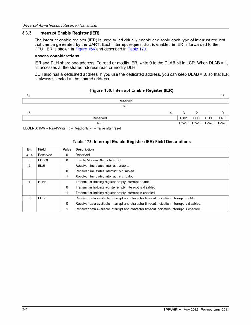
Universal Asynchronous Receiver/Transmitter
8.3.3 Interrupt Enable Register (IER)The interrupt enable register (IER) is used to individually enable or disable each type of interrupt requestthat can be generated by the UART. Each interrupt request that is enabled in IER is forwarded to theCPU. IER is shown in Figure 166 and described in Table 173.
Access considerations:IER and DLH share one address. To read or modify IER, write 0 to the DLAB bit in LCR. When DLAB = 1,all accesses at the shared address read or modify DLH.
DLH also has a dedicated address. If you use the dedicated address, you can keep DLAB = 0, so that IERis always selected at the shared address.
Figure 166. Interrupt Enable Register (IER)31 16
ReservedR-0
15 4 3 2 1 0Reserved Rsvd ELSI ETBEI ERBI
R-0 R/W-0 R/W-0 R/W-0 R/W-0LEGEND: R/W = Read/Write; R = Read only; -n = value after reset
Table 173. Interrupt Enable Register (IER) Field Descriptions
Bit Field Value Description31-4 Reserved 0 Reserved
3 EDSSI 0 Enable Modem Status Interrupt2 ELSI Receiver line status interrupt enable.
0 Receiver line status interrupt is disabled.1 Receiver line status interrupt is enabled.
1 ETBEI Transmitter holding register empty interrupt enable.0 Transmitter holding register empty interrupt is disabled.1 Transmitter holding register empty interrupt is enabled.
0 ERBI Receiver data available interrupt and character timeout indication interrupt enable.0 Receiver data available interrupt and character timeout indication interrupt is disabled.1 Receiver data available interrupt and character timeout indication interrupt is enabled.
240 SPRUHF8A–May 2012–Revised June 2013
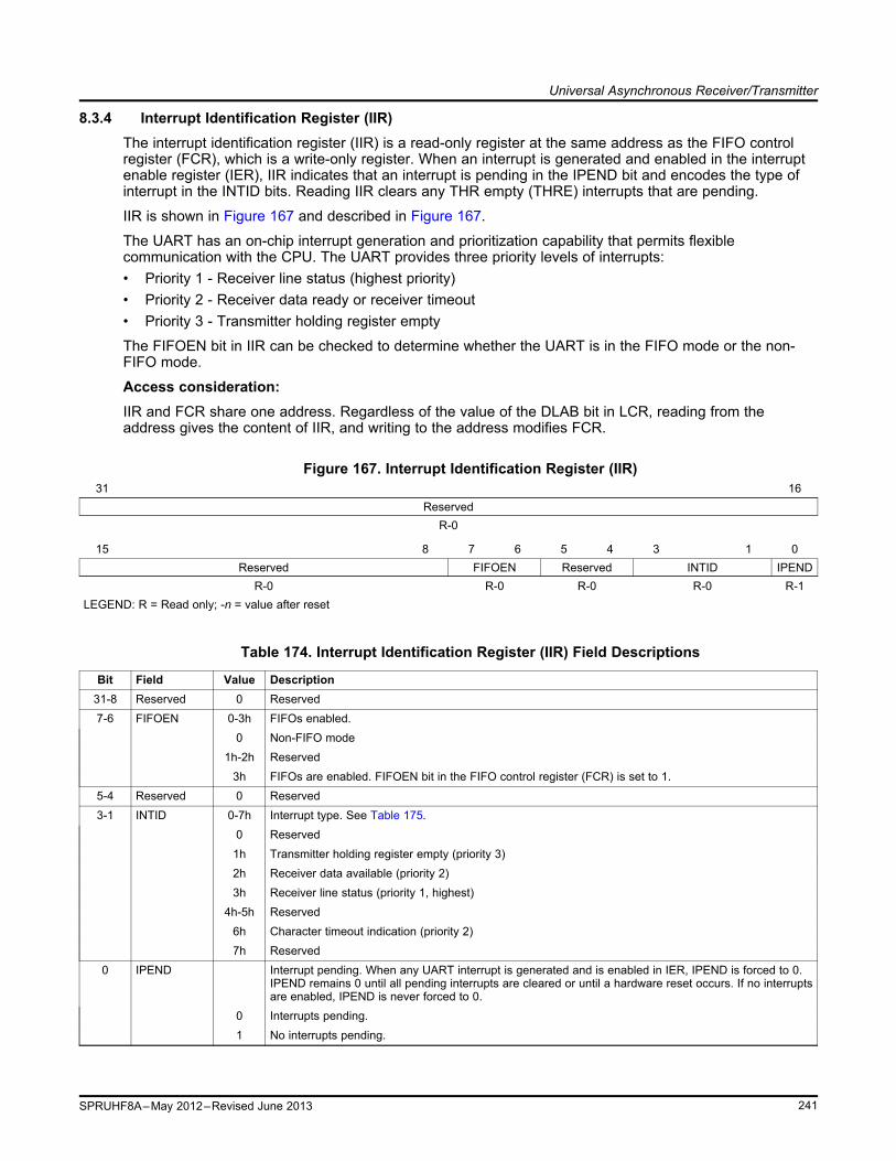
Universal Asynchronous Receiver/Transmitter
8.3.4 Interrupt Identification Register (IIR)The interrupt identification register (IIR) is a read-only register at the same address as the FIFO controlregister (FCR), which is a write-only register. When an interrupt is generated and enabled in the interruptenable register (IER), IIR indicates that an interrupt is pending in the IPEND bit and encodes the type ofinterrupt in the INTID bits. Reading IIR clears any THR empty (THRE) interrupts that are pending.
IIR is shown in Figure 167 and described in Figure 167.
The UART has an on-chip interrupt generation and prioritization capability that permits flexiblecommunication with the CPU. The UART provides three priority levels of interrupts:• Priority 1 - Receiver line status (highest priority)• Priority 2 - Receiver data ready or receiver timeout• Priority 3 - Transmitter holding register empty
The FIFOEN bit in IIR can be checked to determine whether the UART is in the FIFO mode or the non-FIFO mode.
Access consideration:IIR and FCR share one address. Regardless of the value of the DLAB bit in LCR, reading from theaddress gives the content of IIR, and writing to the address modifies FCR.
Figure 167. Interrupt Identification Register (IIR)31 16
ReservedR-0
15 8 7 6 5 4 3 1 0Reserved FIFOEN Reserved INTID IPEND
R-0 R-0 R-0 R-0 R-1LEGEND: R = Read only; -n = value after reset
Table 174. Interrupt Identification Register (IIR) Field Descriptions
Bit Field Value Description31-8 Reserved 0 Reserved7-6 FIFOEN 0-3h FIFOs enabled.
0 Non-FIFO mode1h-2h Reserved
3h FIFOs are enabled. FIFOEN bit in the FIFO control register (FCR) is set to 1.5-4 Reserved 0 Reserved3-1 INTID 0-7h Interrupt type. See Table 175.
0 Reserved1h Transmitter holding register empty (priority 3)2h Receiver data available (priority 2)3h Receiver line status (priority 1, highest)
4h-5h Reserved6h Character timeout indication (priority 2)7h Reserved
0 IPEND Interrupt pending. When any UART interrupt is generated and is enabled in IER, IPEND is forced to 0.IPEND remains 0 until all pending interrupts are cleared or until a hardware reset occurs. If no interruptsare enabled, IPEND is never forced to 0.
0 Interrupts pending.1 No interrupts pending.
241SPRUHF8A–May 2012–Revised June 2013

Universal Asynchronous Receiver/Transmitter
Table 175. Interrupt Identification and Interrupt Clearing InformationIIR BitsPriority
Level 3 2 1 0 Interrupt Type Interrupt Source Event That Clears InterruptNone 0 0 0 1 None None None
1 0 1 1 0 Receiver line status Overrun error, parity error, framing For an overrun error, reading the lineerror, or break is detected. status register (LSR) clears the
interrupt. For a parity error, framingerror, or break, the interrupt iscleared only after all the erroneousdata have been read.
2 0 1 0 0 Receiver data-ready Non-FIFO mode: Receiver data is Non-FIFO mode: The receiver bufferready. register (RBR) is read.FIFO mode: Trigger level reached. If FIFO mode: The FIFO drops belowfour character times (see Table 168) the trigger level. (1)
pass with no access of the FIFO, theinterrupt is asserted again.
2 1 1 0 0 Receiver time-out FIFO mode only: No characters have One of the following events:been removed from or input to the • A character is read from thereceiver FIFO during the last four receiver FIFO. (1)
character times (see Table 168), and • A new character arrives in thethere is at least one character in the receiver FIFO.receiver FIFO during this time.• The URRST bit in the power
and emulation managementregister (PWREMU_MGMT) isloaded with 0.
3 0 0 1 0 Transmitter holding Non-FIFO mode: Transmitter holding A character is written to theregister empty register (THR) is empty. transmitter holding register (THR) or
FIFO mode: Transmitter FIFO is the interrupt identification registerempty. (IIR) is read.
(1) In the FIFO mode, the receiver data-ready interrupt or receiver time-out interrupt is cleared by the CPU or by the DMA controller,whichever reads from the receiver FIFO first.
8.3.5 FIFO Control Register (FCR)The FIFO control register (FCR) is a write-only register at the same address as the interrupt identificationregister (IIR), which is a read-only register. Use FCR to enable and clear the FIFOs and to select thereceiver FIFO trigger level FCR is shown in Figure 168 and described in Table 176. The FIFOEN bit mustbe set to 1 before other FCR bits are written to or the FCR bits are not programmed.
Access consideration:IIR and FCR share one address. Regardless of the value of the DLAB bit, reading from the address givesthe content of IIR, and writing to the address modifies FCR.
CAUTIONFor proper communication between the UART and the EDMA controller, theDMAMODE1 bit must be set to 1. Always write a 1 to the DMAMODE1 bit, andafter a hardware reset, change the DMAMODE1 bit from 0 to 1.
242 SPRUHF8A–May 2012–Revised June 2013

Universal Asynchronous Receiver/Transmitter
Figure 168. FIFO Control Register (FCR)31 16
ReservedR-0
15 8Reserved
R-0
7 6 5 4 3 2 1 0RXFIFTL Reserved DMAMODE1 (1) TXCLR RXCLR FIFOEN
W-0 R-0 W-0 W1C-0 W1C-0 W-0LEGEND: R = Read only; W = Write only; W1C = Write 1 to clear (writing 0 has no effect); -n = value after reset
(1) Always write 1 to the DMAMODE1 bit. After a hardware reset, change the DMAMODE1 bit from 0 to 1. DMAMODE = 1 is required forproper communication between the UART and the DMA controller.
Table 176. FIFO Control Register (FCR) Field Descriptions
Bit Field Value Description31-8 Reserved 0 Reserved7-6 RXFIFTL 0-3h Receiver FIFO trigger level. RXFIFTL sets the trigger level for the receiver FIFO. When the trigger level
is reached, a receiver data-ready interrupt is generated (if the interrupt request is enabled). Once theFIFO drops below the trigger level, the interrupt is cleared.
0 1 byte1h 4 bytes2h 8 bytes3h 14 bytes
5-4 Reserved 0 Reserved3 DMAMODE1 DMA MODE1 enable if FIFOs are enabled. Always write 1 to DMAMODE1. After a hardware reset,
change DMAMODE1 from 0 to 1. DMAMOD1 = 1 is a requirement for proper communication betweenthe UART and the EDMA controller.
0 DMA MODE1 is disabled.1 DMA MODE1 is enabled.
2 TXCLR Transmitter FIFO clear. Write a 1 to TXCLR to clear the bit.0 No effect.1 Clears transmitter FIFO and resets the transmitter FIFO counter. The shift register is not cleared.
1 RXCLR Receiver FIFO clear. Write a 1 to RXCLR to clear the bit.0 No effect.1 Clears receiver FIFO and resets the receiver FIFO counter. The shift register is not cleared.
0 FIFOEN Transmitter and receiver FIFOs mode enable. FIFOEN must be set before other FCR bits are written toor the FCR bits are not programmed. Clearing this bit clears the FIFO counters.
0 Non-FIFO mode. The transmitter and receiver FIFOs are disabled, and the FIFO pointers are cleared.1 FIFO mode. The transmitter and receiver FIFOs are enabled.
243SPRUHF8A–May 2012–Revised June 2013

Universal Asynchronous Receiver/Transmitter
8.3.6 Line Control Register (LCR)The line control register (LCR) is shown in Figure 169 and described in Table 177.
The system programmer controls the format of the asynchronous data communication exchange by usingLCR. In addition, the programmer can retrieve, inspect, and modify the content of LCR; this eliminates theneed for separate storage of the line characteristics in system memory.
Figure 169. Line Control Register (LCR)31 16
ReservedR-0
15 8 7 6 5 4 3 2 1 0Reserved DLAB BC SP EPS PEN STB WLS
R-0 R/W-0 R/W-0 R/W-0 R/W-0 R/W-0 R/W-0 R/W-0LEGEND: R/W = Read/Write; R = Read only; -n = value after reset
Table 177. Line Control Register (LCR) Field Descriptions
Bit Field Value Description31-8 Reserved 0 Reserved
7 DLAB Divisor latch access bit. The divisor latch registers (DLL and DLH) can be accessed at dedicatedaddresses or at addresses shared by RBR, THR, and IER. Using the shared addresses requirestoggling DLAB to change which registers are selected. If you use the dedicated addresses, you cankeep DLAB = 0.
0 Allows access to the receiver buffer register (RBR), the transmitter holding register (THR), and theinterrupt enable register (IER) selected. At the address shared by RBR, THR, and DLL, the CPU canread from RBR and write to THR. At the address shared by IER and DLH, the CPU can read from andwrite to IER.
1 Allows access to the divisor latches of the baud generator during a read or write operation (DLL andDLH). At the address shared by RBR, THR, and DLL, the CPU can read from and write to DLL. At theaddress shared by IER and DLH, the CPU can read from and write to DLH.
6 BC Break control.0 Break condition is disabled.1 Break condition is transmitted to the receiving UART. A break condition is a condition where the
UARTn_TXD signal is forced to the spacing (cleared) state.5 SP Stick parity. The SP bit works in conjunction with the EPS and PEN bits. The relationship between the
SP, EPS, and PEN bits is summarized in Table 178.0 Stick parity is disabled.1 Stick parity is enabled.
• When odd parity is selected (EPS = 0), the PARITY bit is transmitted and checked as set.• When even parity is selected (EPS = 1), the PARITY bit is transmitted and checked as cleared.
4 EPS Even parity select. Selects the parity when parity is enabled (PEN = 1). The EPS bit works inconjunction with the SP and PEN bits. The relationship between the SP, EPS, and PEN bits issummarized in Table 178.
0 Odd parity is selected (an odd number of logic 1s is transmitted or checked in the data and PARITYbits).
1 Even parity is selected (an even number of logic 1s is transmitted or checked in the data and PARITYbits).
3 PEN Parity enable. The PEN bit works in conjunction with the SP and EPS bits. The relationship between theSP, EPS, and PEN bits is summarized in Table 178.
0 No PARITY bit is transmitted or checked.1 Parity bit is generated in transmitted data and is checked in received data between the last data word
bit and the first STOP bit.
244 SPRUHF8A–May 2012–Revised June 2013

Universal Asynchronous Receiver/Transmitter
Table 177. Line Control Register (LCR) Field Descriptions (continued)Bit Field Value Description2 STB Number of STOP bits generated. STB specifies 1, 1.5, or 2 STOP bits in each transmitted character.
When STB = 1, the WLS bit determines the number of STOP bits. The receiver clocks only the firstSTOP bit, regardless of the number of STOP bits selected. The number of STOP bits generated issummarized in Table 179.
0 1 STOP bit is generated.1 WLS bit determines the number of STOP bits:
• When WLS = 0, 1.5 STOP bits are generated.• When WLS = 1h, 2h, or 3h, 2 STOP bits are generated.
1-0 WLS 0-3h Word length select. Number of bits in each transmitted or received serial character. When STB = 1, theWLS bit determines the number of STOP bits.
0 5 bits1h 6 bits2h 7 bits3h 8 bits
Table 178. Relationship Between ST, EPS, and PEN Bits in LCRST Bit EPS Bit PEN Bit Parity Option
x x 0 Parity disabled: No PARITY bit is transmitted or checked0 0 1 Odd parity selected: Odd number of logic 1s0 1 1 Even parity selected: Even number of logic 1s1 0 1 Stick parity selected with PARITY bit transmitted and checked as set1 1 1 Stick parity selected with PARITY bit transmitted and checked as cleared
Table 179. Number of STOP Bits GeneratedWord Length Selected Number of STOP Bits Baud Clock (BCLK)
STB Bit WLS Bits with WLS Bits Generated Cycles0 x Any word length 1 161 0h 5 bits 1.5 241 1h 6 bits 2 321 2h 7 bits 2 321 3h 8 bits 2 32
245SPRUHF8A–May 2012–Revised June 2013

Universal Asynchronous Receiver/Transmitter
8.3.7 Modem Control Register (MCR)The modem control register (MCR) is shown in Figure 170 and described in Table 180. The modemcontrol register provides the ability to enable/disable the autoflow functions, and enable/disable theloopback function for diagnostic purposes.
Figure 170. Modem Control Register (MCR)31 16
ReservedR-0
15 6 5 4 3 2 1 0Reserved AFE (1) LOOP OUT2 OUT1 RTS (1) Rsvd
R-0 R/W-0 R/W-0 R/W-0 R/W-0 R/W-0 R-0LEGEND: R/W = Read/Write; R = Read only; -n = value after reset
(1) All UARTs do not support this feature, see your device-specific data manual for supported features. If this feature is not available, this bitis reserved and should be cleared to 0.
Table 180. Modem Control Register (MCR) Field Descriptions
Bit Field Value Description31-6 Reserved 0 Reserved
5 AFE Autoflow control enable. Autoflow control allows the UARTn_RTS and UARTn_CTS signals to providehandshaking between UARTs during data transfer. When AFE = 1, the RTS bit determines the autoflowcontrol enabled. Note that all UARTs do not support this feature, see your device-specific data manualfor supported features. If this feature is not available, this bit is reserved and should be cleared to 0.
0 Autoflow control is disabled.1 Autoflow control is enabled:
• When RTS = 0, UARTn_CTS is only enabled.• When RTS = 1, UARTn_RTS and UARTn_CTS are enabled.
4 LOOP Loop back mode enable. LOOP is used for the diagnostic testing using the loop back feature.0 Loop back mode is disabled.1 Loop back mode is enabled. When LOOP is set, the following occur:
• The UARTn_TXD signal is set high.• The UARTn_RXD pin is disconnected• The output of the transmitter shift register (TSR) is lopped back in to the receiver shift register (RSR)
input.3 OUT2 0 OUT2 Control Bit2 OUT1 0 OUT1 Control Bit1 RTS RTS control. When AFE = 1, the RTS bit determines the autoflow control enabled. Note that all UARTs
do not support this feature, see your device-specific data manual for supported features. If this featureis not available, this bit is reserved and should be cleared to 0.
0 UARTn_RTS is disabled, UARTn_CTS is only enabled.1 UARTn_RTS and UARTn_CTS are enabled.
0 Reserved 0 Reserved
246 SPRUHF8A–May 2012–Revised June 2013

Universal Asynchronous Receiver/Transmitter
8.3.8 Line Status Register (LSR)The line status register (LSR) is shown in Figure 171 and described in Table 181. LSR providesinformation to the CPU concerning the status of data transfers. LSR is intended for read operations only;do not write to this register. Bits 1 through 4 record the error conditions that produce a receiver line statusinterrupt.
Figure 171. Line Status Register (LSR)31 16
ReservedR-0
15 8 7 6 5 4 3 2 1 0Reserved RXFIFOE TEMT THRE BI FE PE OE DR
R-0 R-0 R-1 R-1 R-0 R-0 R-0 R-0 R-0LEGEND: R = Read only; -n = value after reset
Table 181. Line Status Register (LSR) Field Descriptions
Bit Field Value Description31-8 Reserved 0 Reserved
7 RXFIFOE Receiver FIFO error.In non-FIFO mode:
0 There has been no error, or RXFIFOE was cleared because the CPU read the erroneous characterfrom the receiver buffer register (RBR).
1 There is a parity error, framing error, or break indicator in the receiver buffer register (RBR).In FIFO mode:
0 There has been no error, or RXFIFOE was cleared because the CPU read the erroneous characterfrom the receiver FIFO and there are no more errors in the receiver FIFO.
1 At least one parity error, framing error, or break indicator in the receiver FIFO.6 TEMT Transmitter empty (TEMT) indicator.
In non-FIFO mode:0 Either the transmitter holding register (THR) or the transmitter shift register (TSR) contains a data
character.1 Both the transmitter holding register (THR) and the transmitter shift register (TSR) are empty.
In FIFO mode:0 Either the transmitter FIFO or the transmitter shift register (TSR) contains a data character.1 Both the transmitter FIFO and the transmitter shift register (TSR) are empty.
5 THRE Transmitter holding register empty (THRE) indicator. If the THRE bit is set and the correspondinginterrupt enable bit is set (ETBEI = 1 in IER), an interrupt request is generated.In non-FIFO mode:
0 Transmitter holding register (THR) is not empty. THR has been loaded by the CPU.1 Transmitter holding register (THR) is empty (ready to accept a new character). The content of THR has
been transferred to the transmitter shift register (TSR).In FIFO mode:
0 Transmitter FIFO is not empty. At least one character has been written to the transmitter FIFO. You canwrite to the transmitter FIFO if it is not full.
1 Transmitter FIFO is empty. The last character in the FIFO has been transferred to the transmitter shiftregister (TSR).
247SPRUHF8A–May 2012–Revised June 2013

Universal Asynchronous Receiver/Transmitter
Table 181. Line Status Register (LSR) Field Descriptions (continued)Bit Field Value Description4 BI Break indicator. The BI bit is set whenever the receive data input (UARTn_RXD) was held low for longer
than a full-word transmission time. A full-word transmission time is defined as the total time to transmitthe START, data, PARITY, and STOP bits. If the BI bit is set and the corresponding interrupt enable bitis set (ELSI = 1 in IER), an interrupt request is generated.In non-FIFO mode:
0 No break has been detected, or the BI bit was cleared because the CPU read the erroneous characterfrom the receiver buffer register (RBR).
1 A break has been detected with the character in the receiver buffer register (RBR).In FIFO mode:
0 No break has been detected, or the BI bit was cleared because the CPU read the erroneous characterfrom the receiver FIFO and the next character to be read from the FIFO has no break indicator.
1 A break has been detected with the character at the top of the receiver FIFO.3 FE Framing error (FE) indicator. A framing error occurs when the received character does not have a valid
STOP bit. In response to a framing error, the UART sets the FE bit and waits until the signal on the RXpin goes high. Once the RX signal goes high, the receiver is ready to detect a new START bit andreceive new data. If the FE bit is set and the corresponding interrupt enable bit is set (ELSI = 1 in IER),an interrupt request is generated.In non-FIFO mode:
0 No framing error has been detected, or the FE bit was cleared because the CPU read the erroneousdata from the receiver buffer register (RBR).
1 A framing error has been detected with the character in the receiver buffer register (RBR).In FIFO mode:
0 No framing error has been detected, or the FE bit was cleared because the CPU read the erroneousdata from the receiver FIFO and the next character to be read from the FIFO has no framing error.
1 A framing error has been detected with the character at the top of the receiver FIFO.2 PE Parity error (PE) indicator. A parity error occurs when the parity of the received character does not
match the parity selected with the EPS bit in the line control register (LCR). If the PE bit is set and thecorresponding interrupt enable bit is set (ELSI = 1 in IER), an interrupt request is generated.In non-FIFO mode:
0 No parity error has been detected, or the PE bit was cleared because the CPU read the erroneous datafrom the receiver buffer register (RBR).
1 A parity error has been detected with the character in the receiver buffer register (RBR).In FIFO mode:
0 No parity error has been detected, or the PE bit was cleared because the CPU read the erroneous datafrom the receiver FIFO and the next character to be read from the FIFO has no parity error.
1 A parity error has been detected with the character at the top of the receiver FIFO.1 OE Overrun error (OE) indicator. An overrun error in the non-FIFO mode is different from an overrun error
in the FIFO mode. If the OE bit is set and the corresponding interrupt enable bit is set (ELSI = 1 in IER),an interrupt request is generated.In non-FIFO mode:
0 No overrun error has been detected, or the OE bit was cleared because the CPU read the content ofthe line status register (LSR).
1 Overrun error has been detected. Before the character in the receiver buffer register (RBR) could beread, it was overwritten by the next character arriving in RBR.In FIFO mode:
0 No overrun error has been detected, or the OE bit was cleared because the CPU read the content ofthe line status register (LSR).
1 Overrun error has been detected. If data continues to fill the FIFO beyond the trigger level, an overrunerror occurs only after the FIFO is full and the next character has been completely received in the shiftregister. An overrun error is indicated to the CPU as soon as it happens. The new character overwritesthe character in the shift register, but it is not transferred to the FIFO.
248 SPRUHF8A–May 2012–Revised June 2013

Universal Asynchronous Receiver/Transmitter
Table 181. Line Status Register (LSR) Field Descriptions (continued)Bit Field Value Description0 DR Data-ready (DR) indicator for the receiver. If the DR bit is set and the corresponding interrupt enable bit
is set (ERBI = 1 in IER), an interrupt request is generated.In non-FIFO mode:
0 Data is not ready, or the DR bit was cleared because the character was read from the receiver bufferregister (RBR).
1 Data is ready. A complete incoming character has been received and transferred into the receiver bufferregister (RBR).In FIFO mode:
0 Data is not ready, or the DR bit was cleared because all of the characters in the receiver FIFO havebeen read.
1 Data is ready. There is at least one unread character in the receiver FIFO. If the FIFO is empty, the DRbit is set as soon as a complete incoming character has been received and transferred into the FIFO.The DR bit remains set until the FIFO is empty again.
249SPRUHF8A–May 2012–Revised June 2013

Universal Asynchronous Receiver/Transmitter
8.3.9 Modem Status Register (MSR)The Modem status register (MSR) is shown in Figure 172 and described in Table 182. MSR providesinformation to the CPU concerning the status of modem control signals. MSR is intended for readoperations only; do not write to this register.
Figure 172. Modem Status Register (MSR)31 16
ReservedR-0
15 8 7 6 5 4 3 2 1 0Reserved CD RI DSR CTS DCD TERI DDSR DCTS
R-0 R-0 R-0 R-0 R-0 R-0 R-0 R-0 R-0LEGEND: R = Read only; -n = value after reset
Table 182. Modem Status Register (MSR) Field Descriptions
Bit Field Value Description31-8 Reserved 0 Reserved
7 CD 0 Complement of the Carrier Detect input. When the UART is in the diagnostic test mode (loopback modeMCR[4] = 1), this bit is equal to the MCR bit 3 (OUT2).
6 RI 0 Complement of the Ring Indicator input. When the UART is in the diagnostic test mode (loopback modeMCR[4] = 1), this bit is equal to the MCR bit 2 (OUT1).
5 DSR 0 Complement of the Data Set Ready input. When the UART is in the diagnostic test mode (loopbackmode MCR[4] = 1), this bit is equal to the MCR bit 0 (DTR).
4 CTS 0 Complement of the Clear To Send input. When the UART is in the diagnostic test mode (loopbackmode MCR[4] = 1), this bit is equal to the MCR bit 1 (RTS).
3 DCD 0 Change in DCD indicator bit. DCD indicates that the DCD input has changed state since the last time itwas read by the CPU. When DCD is set and the modem status interrupt is enabled, a modem statusinterrupt is generated.
2 TERI 0 Trailing edge of RI (TERI) indicator bit. TERI indicates that the RI input has changed from a low to ahigh. When TERI is set and the modem status interrupt is enabled, a modem status interrupt isgenerated.
1 DDSR 0 Change in DSR indicator bit. DDSR indicates that the DSR input has changed state since the last time itwas read by the CPU. When DDSR is set and the modem status interrupt is enabled, a modem statusinterrupt is generated.
0 DCTS 0 Change in CTS indicator bit. DCTS indicates that the CTS input has changed state since the last time itwas read by the CPU. When DCTS is set (autoflow control is not enabled and the modem statusinterrupt is enabled), a modem status interrupt is generated. When autoflow control is enabled, nointerrupt is generated.
250 SPRUHF8A–May 2012–Revised June 2013
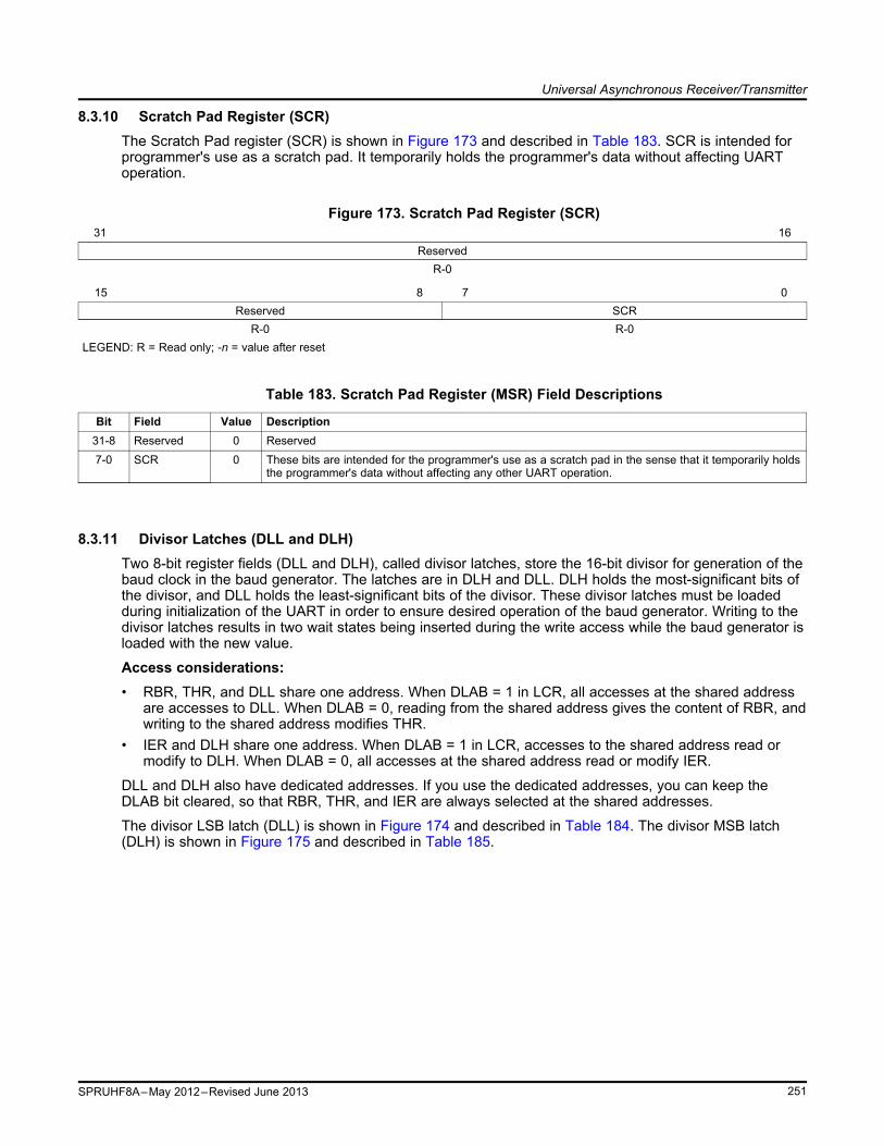
Universal Asynchronous Receiver/Transmitter
8.3.10 Scratch Pad Register (SCR)The Scratch Pad register (SCR) is shown in Figure 173 and described in Table 183. SCR is intended forprogrammer's use as a scratch pad. It temporarily holds the programmer's data without affecting UARToperation.
Figure 173. Scratch Pad Register (SCR)31 16
ReservedR-0
15 8 7 0Reserved SCR
R-0 R-0LEGEND: R = Read only; -n = value after reset
Table 183. Scratch Pad Register (MSR) Field Descriptions
Bit Field Value Description31-8 Reserved 0 Reserved7-0 SCR 0 These bits are intended for the programmer's use as a scratch pad in the sense that it temporarily holds
the programmer's data without affecting any other UART operation.
8.3.11 Divisor Latches (DLL and DLH)Two 8-bit register fields (DLL and DLH), called divisor latches, store the 16-bit divisor for generation of thebaud clock in the baud generator. The latches are in DLH and DLL. DLH holds the most-significant bits ofthe divisor, and DLL holds the least-significant bits of the divisor. These divisor latches must be loadedduring initialization of the UART in order to ensure desired operation of the baud generator. Writing to thedivisor latches results in two wait states being inserted during the write access while the baud generator isloaded with the new value.
Access considerations:• RBR, THR, and DLL share one address. When DLAB = 1 in LCR, all accesses at the shared address
are accesses to DLL. When DLAB = 0, reading from the shared address gives the content of RBR, andwriting to the shared address modifies THR.
• IER and DLH share one address. When DLAB = 1 in LCR, accesses to the shared address read ormodify to DLH. When DLAB = 0, all accesses at the shared address read or modify IER.
DLL and DLH also have dedicated addresses. If you use the dedicated addresses, you can keep theDLAB bit cleared, so that RBR, THR, and IER are always selected at the shared addresses.
The divisor LSB latch (DLL) is shown in Figure 174 and described in Table 184. The divisor MSB latch(DLH) is shown in Figure 175 and described in Table 185.
251SPRUHF8A–May 2012–Revised June 2013

Universal Asynchronous Receiver/Transmitter
Figure 174. Divisor LSB Latch (DLL)31 16
ReservedR-0
15 8 7 0Reserved DLL
R-0 R/W-0LEGEND: R/W = Read/Write; R = Read only; -n = value after reset
Table 184. Divisor LSB Latch (DLL) Field Descriptions
Bit Field Value Description31-8 Reserved 0 Reserved7-0 DLL 0-Fh The 8 least-significant bits (LSBs) of the 16-bit divisor for generation of the baud clock in the baud rate
generator.
Figure 175. Divisor MSB Latch (DLH)31 16
ReservedR-0
15 8 7 0Reserved DLH
R-0 R/W-0LEGEND: R/W = Read/Write; R = Read only; -n = value after reset
Table 185. Divisor MSB Latch (DLH) Field Descriptions
Bit Field Value Description31-8 Reserved 0 Reserved7-0 DLH 0-Fh The 8 most-significant bits (MSBs) of the 16-bit divisor for generation of the baud clock in the baud rate
generator.
252 SPRUHF8A–May 2012–Revised June 2013

Universal Asynchronous Receiver/Transmitter
8.3.12 Revision Identification Registers (REVID1 and REVID2)The revision identification registers (REVID1 and REVID2) contain peripheral identification data for theperipheral. REVID1 is shown in Figure 176 and described in Table 186. REVID2 is shown in Figure 177and described in Table 187.
Figure 176. Revision Identification Register 1 (REVID1)31 0
REVID1R-1102 0002h
LEGEND: R = Read only; -n = value after reset
Table 186. Revision Identification Register 1 (REVID1) Field Descriptions
Bit Field Value Description31-0 REVID1 1102 0002h Peripheral Identification Number
Figure 177. Revision Identification Register 2 (REVID2)31 16
ReservedR-0
15 8 7 0Reserved REVID2
R-0 R-0LEGEND: R = Read only; -n = value after reset
Table 187. Revision Identification Register 2 (REVID2) Field Descriptions
Bit Field Value Description31-8 Reserved 0 Reserved7-0 REVID2 0 Peripheral Identification Number
253SPRUHF8A–May 2012–Revised June 2013

Universal Asynchronous Receiver/Transmitter
8.3.13 Power and Emulation Management Register (PWREMU_MGMT)The power and emulation management register (PWREMU_MGMT) is shown in Figure 178 and describedin Table 188.
Figure 178. Power and Emulation Management Register (PWREMU_MGMT)31 16
ReservedR-0
15 14 13 12 1 0Rsvd UTRST URRST Reserved FREE
R/W-0 R/W-0 R/W-0 R-1 R/W-0LEGEND: R/W = Read/Write; R = Read only; -n = value after reset
Table 188. Power and Emulation Management Register (PWREMU_MGMT) Field Descriptions
Bit Field Value Description31-16 Reserved 0 Reserved
15 Reserved 0 Reserved. This bit must always be written with a 0.14 UTRST UART transmitter reset. Resets and enables the transmitter.
0 Transmitter is disabled and in reset state.1 Transmitter is enabled.
13 URRST UART receiver reset. Resets and enables the receiver.0 Receiver is disabled and in reset state.1 Receiver is enabled.
12-1 Reserved 1 Reserved0 FREE Free-running enable mode bit. This bit determines the emulation mode functionality of the UART. When
halted, the UART can handle register read/write requests, but does not generate anytransmission/reception, interrupts or events.
0 If a transmission is not in progress, the UART halts immediately. If a transmission is in progress, theUART halts after completion of the one-word transmission.
1 Free-running mode is enabled; UART continues to run normally.
254 SPRUHF8A–May 2012–Revised June 2013

Universal Asynchronous Receiver/Transmitter
8.3.14 Mode Definition Register (MDR)The Mode Definition register (MDR) determines the over-sampling mode for the UART. MDR is shown inFigure 179 and described in Table 189.
Figure 179. Mode Definition Register (MDR)31 16
ReservedR-0
15 1 0Reserved OSM_SEL
R-0 R/W-0LEGEND: R/W = Read/Write; R = Read only; -n = value after reset
Table 189. Mode Definition Register (MDR) Field Descriptions
Bit Field Value Description31-1 Reserved 0 Reserved
0 OSM_SEL Over-Sampling Mode Select.0 16× over-sampling.1 13× over-sampling.
255SPRUHF8A–May 2012–Revised June 2013
Industrial Ethernet Peripheral (IEP)
9 Industrial Ethernet Peripheral (IEP)
9.1 Introduction
The industrial ethernet peripheral (IEP) is intended to do the hardware work required for industrial ethernetfunctions. The IEP module features an industrial ethernet timer with eight compare events.
9.2 Functional Description
9.2.1 Clock GenerationThe IEP has a dedicated input clock with a configurable clock source. Two clock sources are supportedfor the IEP input clock:• iep_clk (default): Runs at 200 MHz.• ocp_clk: Programmable through the IEPCLK register of the PRU-ICSS CFG register space. When
software enables the ocp_clk (OCP_EN), no transactions must be accruing to the IEP block.
Switching from iep_clk to ocp_clk is only supported in software. Switching back from ocp_clk to iep_clk isonly supported through a hardware reset of the PRU-ICSS.
9.2.2 Industrial Ethernet TimerThe industrial ethernet timer is a simple 32-bit timer. This timer is intended for use by industrial ethernetfunctions but can also be leveraged as a generic timer in other applications.
9.2.2.1 Features
The industrial ethernet timer supports the following features:• One master 32-bit count-up counter with an overflow status bit.
– Runs on ocp_clk 200 MHz.– Write 1 to clear status.– Supports a programmable increment value from 1 to 16 (default 5).– An optional compensation method allows the increment value to apply a compensation increment
value from 1 to 16, counting up to 2^24 iep_clk/ocp_clk events.• Eight 32-bit compare registers (CMP[8:0], CMP_STAT).
– Eight status bits, write 1 to clear.– Eight individual event outputs.– One global event (any compare event) output for interrupt generation triggered by any compare
event.• 16 outputs, one high level and one high pulse for each compare hit event.• CMP[0], if enabled, will reset the counter.
9.3 PRU_ICSS_IEP Registers
Table 190 lists the memory-mapped registers for the PRU_ICSS_IEP. All register offset addresses notlisted in Table 190 should be considered as reserved locations and the register contents should not bemodified.
Table 190. PRU_ICSS_IEP REGISTERSOffset Acronym Register Name Section
0h GLOBAL_CFG Section 9.3.14h GLOBAL_STATUS Section 9.3.28h COMPEN Section 9.3.3Ch COUNT Section 9.3.4
256 SPRUHF8A–May 2012–Revised June 2013

Industrial Ethernet Peripheral (IEP)
Table 190. PRU_ICSS_IEP REGISTERS (continued)Offset Acronym Register Name Section
40h CMP_CFG Section 9.3.544h CMP_STATUS Section 9.3.648h CMP0 Section 9.3.74Ch CMP1 Section 9.3.850h CMP2 Section 9.3.954h CMP3 Section 9.3.1058h CMP4 Section 9.3.115Ch CMP5 Section 9.3.1260h CMP6 Section 9.3.1364h CMP7 Section 9.3.14
257SPRUHF8A–May 2012–Revised June 2013

Industrial Ethernet Peripheral (IEP)
9.3.1 GLOBAL_CFG Register (offset = 0h) [reset = 550h]GLOBAL_CFG is shown in Figure 180 and described in Table 191.
GLOBAL CONFIGURE
Figure 180. GLOBAL_CFG Register31 30 29 28 27 26 25 24
Reserved
R-0h
23 22 21 20 19 18 17 16
Reserved
R-0h
15 14 13 12 11 10 9 8
Reserved CMP_INC
R-0h R/W-5h
7 6 5 4 3 2 1 0
DEFAULT_INC Reserved CNT_ENABLE
R/W-5h R-0h R/W-0h
LEGEND: R/W = Read/Write; R = Read only; W1toCl = Write 1 to clear bit; -n = value after reset
Table 191. GLOBAL_CFG Register Field Descriptions
Bit Field Type Reset Description31-12 Reserved R 0h11-8 CMP_INC R/W 5h Defines the increment value when compensation is active7-4 DEFAULT_INC R/W 5h Defines the default increment value3-1 Reserved R 0h0 CNT_ENABLE R/W 0h Counter enable
0: Disables the counter.The counter maintains the current count.1: Enables the counter.
258 SPRUHF8A–May 2012–Revised June 2013

Industrial Ethernet Peripheral (IEP)
9.3.2 GLOBAL_STATUS Register (offset = 4h) [reset = 0h]GLOBAL_STATUS is shown in Figure 181 and described in Table 192.
GLOBAL STATUS
Figure 181. GLOBAL_STATUS Register31 30 29 28 27 26 25 24
Reserved
R-0h
23 22 21 20 19 18 17 16
Reserved
R-0h
15 14 13 12 11 10 9 8
Reserved
R-0h
7 6 5 4 3 2 1 0
Reserved CNT_OVF
R-0h R/W1toClr-0h
LEGEND: R/W = Read/Write; R = Read only; W1toClr = Write 1 to clear bit; -n = value after reset
Table 192. GLOBAL_STATUS Register Field Descriptions
Bit Field Type Reset Description31-1 Reserved R 0h
0 CNT_OVF R/W1toClr 0h Counter overflow status.0: No overflow1: Overflow occurred
259SPRUHF8A–May 2012–Revised June 2013

Industrial Ethernet Peripheral (IEP)
9.3.3 COMPEN Register (offset = 8h) [reset = 0h]COMPEN is shown in Figure 182 and described in Table 193.
COMPENSATION
Figure 182. COMPEN Register31 30 29 28 27 26 25 24
Reserved
R-0h
23 22 21 20 19 18 17 16
COMPEN_CNT
R/W-0h
15 14 13 12 11 10 9 8
COMPEN_CNT
R/W-0h
7 6 5 4 3 2 1 0
COMPEN_CNT
R/W-0h
LEGEND: R/W = Read/Write; R = Read only; W1toCl = Write 1 to clear bit; -n = value after reset
Table 193. COMPEN Register Field Descriptions
Bit Field Type Reset Description31-24 Reserved R 0h23-0 COMPEN_CNT R/W 0h Compensation counter.
Read returns the current COMPEN_CNT value.0: Compensation is disabled and counter will increment byDEFAULT_INC.n: Compensation is enabled until COMPEN_CNT decrements to 0.The COMPEN_CNT value decrements on every iep_clk cycle.When COMPEN_CNT is greater than 0, then count value incrementsby CMP_INC.
260 SPRUHF8A–May 2012–Revised June 2013

Industrial Ethernet Peripheral (IEP)
9.3.4 COUNT Register (offset = Ch) [reset = 0h]COUNT is shown in Figure 183 and described in Table 194.
COUNT is a free running counter with a sticky over flag status bit. The counter over flow flag will be setwhen the counter switches/rollover from 0xffff_ffff -> 0x0000_0000 and continue to count up. The softwarewill need to read and clear the counter over flow flag and increment the MSB in software variable.
Figure 183. COUNT Register31 30 29 28 27 26 25 24 23 22 21 20 19 18 17 16 15 14 13 12 11 10 9 8 7 6 5 4 3 2 1 0
COUNT
R/W1toClr-0h
LEGEND: R/W = Read/Write; R = Read only; W1toCl = Write 1 to clear bit; -n = value after reset
Table 194. COUNT Register Field Descriptions
Bit Field Type Reset Description31-0 COUNT R/W1toClr 0h 32-bit count value.
Increments by (DEFAULT_INC or CMP_INC) on every positive edgeof iep_clk (200MHz).
261SPRUHF8A–May 2012–Revised June 2013

Industrial Ethernet Peripheral (IEP)
9.3.5 CMP_CFG Register (offset = 40h) [reset = 0h]CMP_CFG is shown in Figure 184 and described in Table 195.
COMPARE CONFIGURE
Figure 184. CMP_CFG Register31 30 29 28 27 26 25 24
Reserved
R-0h
23 22 21 20 19 18 17 16
Reserved
R-0h
15 14 13 12 11 10 9 8
Reserved CMP_EN
R-0h R/W-0h
7 6 5 4 3 2 1 0
CMP_EN CMP0_RST_CNT_EN
R/W-0h R/W-0h
LEGEND: R/W = Read/Write; R = Read only; W1toCl = Write 1 to clear bit; -n = value after reset
Table 195. CMP_CFG Register Field Descriptions
Bit Field Type Reset Description31-9 Reserved R 0h8-1 CMP_EN R/W 0h Compare registers enable, where CMP_EN[n] maps to CMP[n]
0: Disables event1: Enables event
0 CMP0_RST_CNT_EN R/W 0h Counter reset enable.0: Disable1: Enable the reset of the counter if a CMP0 event occurs
262 SPRUHF8A–May 2012–Revised June 2013

Industrial Ethernet Peripheral (IEP)
9.3.6 CMP_STATUS Register (offset = 44h) [reset = 0h]CMP_STATUS is shown in Figure 185 and described in Table 196.
COMPARE STATUS
Figure 185. CMP_STATUS Register31 30 29 28 27 26 25 24
Reserved
R-0h
23 22 21 20 19 18 17 16
Reserved
R-0h
15 14 13 12 11 10 9 8
Reserved
R-0h
7 6 5 4 3 2 1 0
CMP_HIT
R/W1toClr-0h
LEGEND: R/W = Read/Write; R = Read only; W1toCl = Write 1 to clear bit; -n = value after reset
Table 196. CMP_STATUS Register Field Descriptions
Bit Field Type Reset Description31-8 Reserved R 0h7-0 CMP_HIT R/W1toClr 0h Status bit for each of the compare registers, where CMP_HIT[n]
maps to CMP[n].Note Match means the current counter is greater than or equal to thecompare value.0: Match has not occurred1: Match occurred.The associated hardware event signal will assert and remain highuntil the status is cleared
263SPRUHF8A–May 2012–Revised June 2013

Industrial Ethernet Peripheral (IEP)
9.3.7 CMP0 Register (offset = 48h) [reset = 0h]CMP0 is shown in Figure 186 and described in Table 197.
COMPARE0
Figure 186. CMP0 Register31 30 29 28 27 26 25 24 23 22 21 20 19 18 17 16 15 14 13 12 11 10 9 8 7 6 5 4 3 2 1 0
CMP0
R/W-0h
LEGEND: R/W = Read/Write; R = Read only; W1toCl = Write 1 to clear bit; -n = value after reset
Table 197. CMP0 Register Field Descriptions
Bit Field Type Reset Description31-0 CMP0 R/W 0h Compare 0 value
264 SPRUHF8A–May 2012–Revised June 2013

Industrial Ethernet Peripheral (IEP)
9.3.8 CMP1 Register (offset = 4Ch) [reset = 0h]CMP1 is shown in Figure 187 and described in Table 198.
COMPARE1
Figure 187. CMP1 Register31 30 29 28 27 26 25 24 23 22 21 20 19 18 17 16 15 14 13 12 11 10 9 8 7 6 5 4 3 2 1 0
CMP1
R/W-0h
LEGEND: R/W = Read/Write; R = Read only; W1toCl = Write 1 to clear bit; -n = value after reset
Table 198. CMP1 Register Field Descriptions
Bit Field Type Reset Description31-0 CMP1 R/W 0h Compare 1 value
265SPRUHF8A–May 2012–Revised June 2013

Industrial Ethernet Peripheral (IEP)
9.3.9 CMP2 Register (offset = 50h) [reset = 0h]CMP2 is shown in Figure 188 and described in Table 199.
COMPARE2
Figure 188. CMP2 Register31 30 29 28 27 26 25 24 23 22 21 20 19 18 17 16 15 14 13 12 11 10 9 8 7 6 5 4 3 2 1 0
CMP2
R/W-0h
LEGEND: R/W = Read/Write; R = Read only; W1toCl = Write 1 to clear bit; -n = value after reset
Table 199. CMP2 Register Field Descriptions
Bit Field Type Reset Description31-0 CMP2 R/W 0h Compare 2 value
266 SPRUHF8A–May 2012–Revised June 2013

Industrial Ethernet Peripheral (IEP)
9.3.10 CMP3 Register (offset = 54h) [reset = 0h]CMP3 is shown in Figure 189 and described in Table 200.
COMPARE3
Figure 189. CMP3 Register31 30 29 28 27 26 25 24 23 22 21 20 19 18 17 16 15 14 13 12 11 10 9 8 7 6 5 4 3 2 1 0
CMP3
R/W-0h
LEGEND: R/W = Read/Write; R = Read only; W1toCl = Write 1 to clear bit; -n = value after reset
Table 200. CMP3 Register Field Descriptions
Bit Field Type Reset Description31-0 CMP3 R/W 0h Compare 3 value
267SPRUHF8A–May 2012–Revised June 2013

Industrial Ethernet Peripheral (IEP)
9.3.11 CMP4 Register (offset = 58h) [reset = 0h]CMP4 is shown in Figure 190 and described in Table 201.
COMPARE4
Figure 190. CMP4 Register31 30 29 28 27 26 25 24 23 22 21 20 19 18 17 16 15 14 13 12 11 10 9 8 7 6 5 4 3 2 1 0
CMP4
R/W-0h
LEGEND: R/W = Read/Write; R = Read only; W1toCl = Write 1 to clear bit; -n = value after reset
Table 201. CMP4 Register Field Descriptions
Bit Field Type Reset Description31-0 CMP4 R/W 0h Compare 4 value
268 SPRUHF8A–May 2012–Revised June 2013

Industrial Ethernet Peripheral (IEP)
9.3.12 CMP5 Register (offset = 5Ch) [reset = 0h]CMP5 is shown in Figure 191 and described in Table 202.
COMPARE5
Figure 191. CMP5 Register31 30 29 28 27 26 25 24 23 22 21 20 19 18 17 16 15 14 13 12 11 10 9 8 7 6 5 4 3 2 1 0
CMP5
R/W-0h
LEGEND: R/W = Read/Write; R = Read only; W1toCl = Write 1 to clear bit; -n = value after reset
Table 202. CMP5 Register Field Descriptions
Bit Field Type Reset Description31-0 CMP5 R/W 0h Compare 5 value
269SPRUHF8A–May 2012–Revised June 2013

Industrial Ethernet Peripheral (IEP)
9.3.13 CMP6 Register (offset = 60h) [reset = 0h]CMP6 is shown in Figure 192 and described in Table 203.
COMPARE6
Figure 192. CMP6 Register31 30 29 28 27 26 25 24 23 22 21 20 19 18 17 16 15 14 13 12 11 10 9 8 7 6 5 4 3 2 1 0
CMP6
R/W-0h
LEGEND: R/W = Read/Write; R = Read only; W1toCl = Write 1 to clear bit; -n = value after reset
Table 203. CMP6 Register Field Descriptions
Bit Field Type Reset Description31-0 CMP6 R/W 0h Compare 6 value
270 SPRUHF8A–May 2012–Revised June 2013

Industrial Ethernet Peripheral (IEP)
9.3.14 CMP7 Register (offset = 64h) [reset = 0h]CMP7 is shown in Figure 193 and described in Table 204.
COMPARE7
Figure 193. CMP7 Register31 30 29 28 27 26 25 24 23 22 21 20 19 18 17 16 15 14 13 12 11 10 9 8 7 6 5 4 3 2 1 0
CMP7
R/W-0h
LEGEND: R/W = Read/Write; R = Read only; W1toCl = Write 1 to clear bit; -n = value after reset
Table 204. CMP7 Register Field Descriptions
Bit Field Type Reset Description31-0 CMP7 R/W 0h Compare 7 value
271SPRUHF8A–May 2012–Revised June 2013

CFG
10 CFGThe PRU-ICSS CFG block contains the registers for control and status of power management, memoryparity, and enhanced PRU GP ports functions. See the following register sections for details.
10.1 PRU_ICSS_CFG Registers
Table 205 lists the memory-mapped registers for the PRU_ICSS_CFG. All register offset addresses notlisted in Table 205 should be considered as reserved locations and the register contents should not bemodified.
Table 205. PRU_ICSS_CFG REGISTERSOffset Acronym Register Name Section
0h REVID Section 10.1.14h SYSCFG Section 10.1.28h GPCFG0 Section 10.1.3Ch GPCFG1 Section 10.1.410h CGR Section 10.1.514h ISRP Section 10.1.618h ISP Section 10.1.71Ch IESP Section 10.1.820h IECP Section 10.1.928h PMAO Section 10.1.102Ch MII_RT Section 10.1.1130h IEPCLK Section 10.1.1234h SPP Section 10.1.1340h PIN_MX Section 10.1.14
272 SPRUHF8A–May 2012–Revised June 2013

CFG
10.1.1 REVID Register (offset = 0h) [reset = 47000000h]REVID is shown in Figure 194 and described in Table 206.
The Revision Register contains the ID and revision information.
Figure 194. REVID Register31 30 29 28 27 26 25 24 23 22 21 20 19 18 17 16 15 14 13 12 11 10 9 8 7 6 5 4 3 2 1 0
REVID
R-47000000h
LEGEND: R/W = Read/Write; R = Read only; W1toCl = Write 1 to clear bit; -n = value after reset
Table 206. REVID Register Field Descriptions
Bit Field Type Reset Description31-0 REVID R 47000000h Revision ID
273SPRUHF8A–May 2012–Revised June 2013

CFG
10.1.2 SYSCFG Register (offset = 4h) [reset = 1Ah]SYSCFG is shown in Figure 195 and described in Table 207.
The System Configuration Register defines the power IDLE and STANDBY modes.
Figure 195. SYSCFG Register31 30 29 28 27 26 25 24
Reserved
R-0h
23 22 21 20 19 18 17 16
Reserved
R-0h
15 14 13 12 11 10 9 8
Reserved
R-0h
7 6 5 4 3 2 1 0
Reserved SUB_MWAIT STANDBY_INIT STANDBY_MODE IDLE_MODE
R-0h R-0h R/W-1h R/W-2h R/W-2h
LEGEND: R/W = Read/Write; R = Read only; W1toCl = Write 1 to clear bit; -n = value after reset
Table 207. SYSCFG Register Field Descriptions
Bit Field Type Reset Description31-6 Reserved R 0h
5 SUB_MWAIT R 0h Status bit for wait state.0 = Ready for Transaction1 = Wait until 0
4 STANDBY_INIT R/W 1h 1 = Initiate standby sequence.0 = Enable OCP master ports.
3-2 STANDBY_MODE R/W 2h 0h = Force standby mode: Initiator unconditionally in standby(standby = 1).1h = No standby mode: Initiator unconditionally out of standby(standby = 0).2h = Smart standby mode: Standby requested by initiator dependingon internal conditions.3h = Reserved.
1-0 IDLE_MODE R/W 2h 0h = Force-idle mode.1h = No-idle mode.2h = Smart-idle mode.3h = Reserved.
274 SPRUHF8A–May 2012–Revised June 2013

CFG
10.1.3 GPCFG0 Register (offset = 8h) [reset = 0h]GPCFG0 is shown in Figure 196 and described in Table 208.
The General Purpose Configuration 0 Register defines the GPI/O configuration for PRU0.
Figure 196. GPCFG0 Register31 30 29 28 27 26 25 24
Reserved PRU0_GPO_SH_SEL PRU0_GPO_DIV1
R-0h R-0h R/W-0h
23 22 21 20 19 18 17 16
PRU0_GPO_DIV1 PRU0_GPO_DIV0
R/W-0h R/W-0h
15 14 13 12 11 10 9 8
PRU0_GPO_DIV0 PRU0_GPO_MODE PRU0_GPI_SB PRU0_GPI_DIV1
R/W-0h R/W-0h 0h R/W-0h
7 6 5 4 3 2 1 0
PRU0_GPI_DIV0 PRU0_GPI_CLK_MO PRU0_GPI_MODEDE
R/W-0h R/W-0h R/W-0h
LEGEND: R/W = Read/Write; R = Read only; W1toCl = Write 1 to clear bit; -n = value after reset
Table 208. GPCFG0 Register Field Descriptions
Bit Field Type Reset Description31-26 Reserved R 0h
25 PRU0_GPO_SH_SEL R 0h Defines which shadow register is currently getting used for GPOshifting.0 = gpo_sh0 is selected1 = gpo_sh1 is selected
24-20 PRU0_GPO_DIV1 R/W 0h Divisor value (divide by PRU0_GPO_DIV1 + 1).0h = div 1.0.1h = div 1.5.2h = div 2.0...1eh = div 16.0.1fh = reserved.
19-15 PRU0_GPO_DIV0 R/W 0h Divisor value (divide by PRU0_GPO_DIV0 + 1).0h = div 1.0.1h = div 1.5.2h = div 2.0...1eh = div 16.0.1fh = reserved.
14 PRU0_GPO_MODE R/W 0h 0 = Direct output mode1 = Serial output mode
13 PRU0_GPI_SB 0h Start Bit event for 28-bit shift mode.PRU0_GPI_SB (pru0_r31_status[29]) is set when first capture of a 1on pru0_r31_status[0].Read 1: Start Bit event occurred.Read 0: Start Bit event has not occurred.Write 1: Will clear PRU0_GPI_SB and clear the whole shift register.Write 0: No Effect.
12-8 PRU0_GPI_DIV1 R/W 0h Divisor value (divide by PRU0_GPI_DIV1 + 1).0h = div 1.0.1h = div 1.5.2h = div 2.0...1eh = div 16.0.1fh = reserved.
275SPRUHF8A–May 2012–Revised June 2013

CFG
Table 208. GPCFG0 Register Field Descriptions (continued)Bit Field Type Reset Description7-3 PRU0_GPI_DIV0 R/W 0h Divisor value (divide by PRU0_GPI_DIV0 + 1).
0h = div 1.0.1h = div 1.5.2h = div 2.0...1eh = div 16.0.1fh = reserved.
2 PRU0_GPI_CLK_MODE R/W 0h Parallel16-bit capture mode clock edge.0 = Use the positive edge of pru0_r31_status[16]1 = Use the negative edge of pru0_r31_status[16]
1-0 PRU0_GPI_MODE R/W 0h 0h = Direct connection mode.1h =16-bit parallel capture mode.2h =28-bit shift mode.3h = Mii_rt mode.
276 SPRUHF8A–May 2012–Revised June 2013
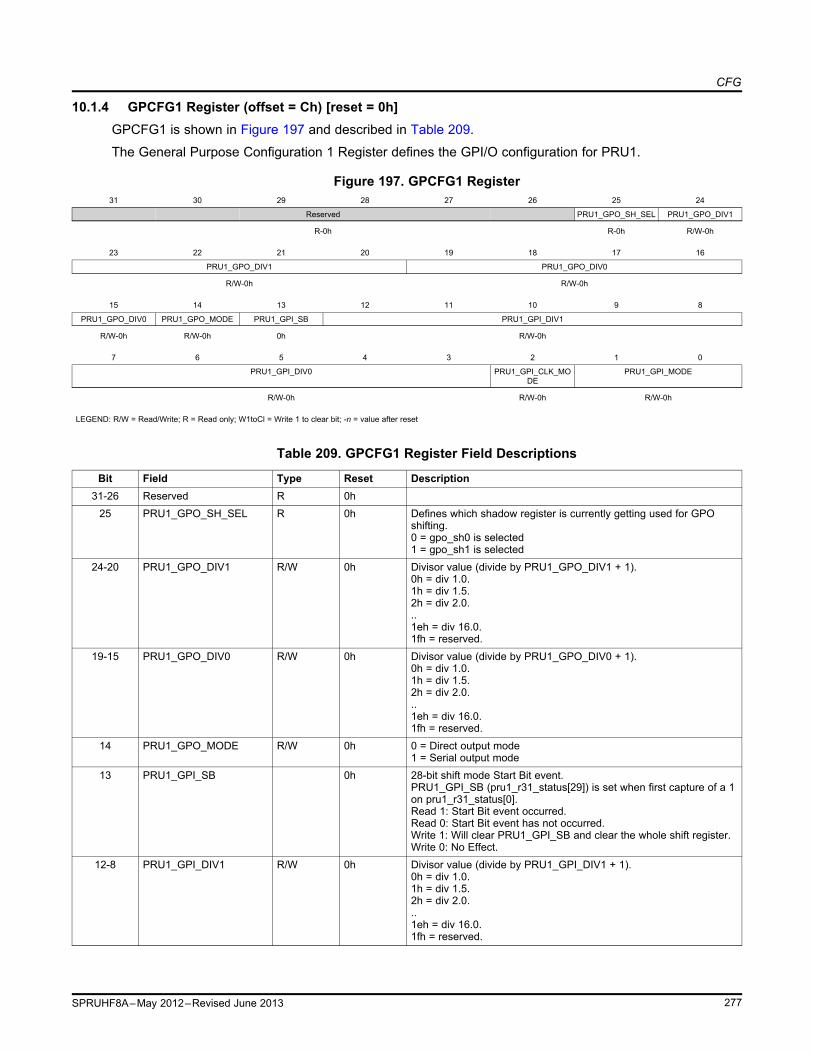
CFG
10.1.4 GPCFG1 Register (offset = Ch) [reset = 0h]GPCFG1 is shown in Figure 197 and described in Table 209.
The General Purpose Configuration 1 Register defines the GPI/O configuration for PRU1.
Figure 197. GPCFG1 Register31 30 29 28 27 26 25 24
Reserved PRU1_GPO_SH_SEL PRU1_GPO_DIV1
R-0h R-0h R/W-0h
23 22 21 20 19 18 17 16
PRU1_GPO_DIV1 PRU1_GPO_DIV0
R/W-0h R/W-0h
15 14 13 12 11 10 9 8
PRU1_GPO_DIV0 PRU1_GPO_MODE PRU1_GPI_SB PRU1_GPI_DIV1
R/W-0h R/W-0h 0h R/W-0h
7 6 5 4 3 2 1 0
PRU1_GPI_DIV0 PRU1_GPI_CLK_MO PRU1_GPI_MODEDE
R/W-0h R/W-0h R/W-0h
LEGEND: R/W = Read/Write; R = Read only; W1toCl = Write 1 to clear bit; -n = value after reset
Table 209. GPCFG1 Register Field Descriptions
Bit Field Type Reset Description31-26 Reserved R 0h
25 PRU1_GPO_SH_SEL R 0h Defines which shadow register is currently getting used for GPOshifting.0 = gpo_sh0 is selected1 = gpo_sh1 is selected
24-20 PRU1_GPO_DIV1 R/W 0h Divisor value (divide by PRU1_GPO_DIV1 + 1).0h = div 1.0.1h = div 1.5.2h = div 2.0...1eh = div 16.0.1fh = reserved.
19-15 PRU1_GPO_DIV0 R/W 0h Divisor value (divide by PRU1_GPO_DIV0 + 1).0h = div 1.0.1h = div 1.5.2h = div 2.0...1eh = div 16.0.1fh = reserved.
14 PRU1_GPO_MODE R/W 0h 0 = Direct output mode1 = Serial output mode
13 PRU1_GPI_SB 0h 28-bit shift mode Start Bit event.PRU1_GPI_SB (pru1_r31_status[29]) is set when first capture of a 1on pru1_r31_status[0].Read 1: Start Bit event occurred.Read 0: Start Bit event has not occurred.Write 1: Will clear PRU1_GPI_SB and clear the whole shift register.Write 0: No Effect.
12-8 PRU1_GPI_DIV1 R/W 0h Divisor value (divide by PRU1_GPI_DIV1 + 1).0h = div 1.0.1h = div 1.5.2h = div 2.0...1eh = div 16.0.1fh = reserved.
277SPRUHF8A–May 2012–Revised June 2013

CFG
Table 209. GPCFG1 Register Field Descriptions (continued)Bit Field Type Reset Description7-3 PRU1_GPI_DIV0 R/W 0h Divisor value (divide by PRU1_GPI_DIV0 + 1).
0h = div 1.0.1h = div 1.5.2h = div 2.0...1eh = div 16.0.1fh = reserved.
2 PRU1_GPI_CLK_MODE R/W 0h Parallel16-bit capture mode clock edge.0 = Use the positive edge of pru1_r31_status[16]1 = Use the negative edge of pru1_r31_status[16]
1-0 PRU1_GPI_MODE R/W 0h 0h = Direct connection mode.1h =16-bit parallel capture mode.2h =28-bit shift mode.3h = Mii_rt mode.
278 SPRUHF8A–May 2012–Revised June 2013

CFG
10.1.5 CGR Register (offset = 10h) [reset = 24924h]CGR is shown in Figure 198 and described in Table 210.
The Clock Gating Register controls the state of Clock Management of the different modules. Softwareshould not clear {module}_CLK_EN until {module}_CLK_STOP_ACK is 0x1.
Figure 198. CGR Register31 30 29 28 27 26 25 24
Reserved
R-0h
23 22 21 20 19 18 17 16
Reserved IEP_CLK_EN IEP_CLK_STOP_ACK
R-0h R/W-1h R-0h
15 14 13 12 11 10 9 8
IEP_CLK_STOP_RE ECAP_CLK_EN ECAP_CLK_STOP_A ECAP_CLK_STOP_R UART_CLK_EN UART_CLK_STOP_A UART_CLK_STOP_R INTC_CLK_ENQ CK EQ CK EQ
R/W-0h R/W-1h R-0h R/W-0h R/W-1h R-0h R/W-0h R/W-1h
7 6 5 4 3 2 1 0
INTC_CLK_STOP_AC INTC_CLK_STOP_RE PRU1_CLK_EN PRU1_CLK_STOP_A PRU1_CLK_STOP_R PRU0_CLK_EN PRU0_CLK_STOP_A PRU0_CLK_STOP_RK Q CK EQ CK EQ
R-0h R/W-0h R/W-1h R-0h R/W-0h R/W-1h R-0h R/W-0h
LEGEND: R/W = Read/Write; R = Read only; W1toCl = Write 1 to clear bit; -n = value after reset
Table 210. CGR Register Field Descriptions
Bit Field Type Reset Description31-18 Reserved R 0h
17 IEP_CLK_EN R/W 1h IEP clock enable.0 = Disable Clock1 = Enable Clock
16 IEP_CLK_STOP_ACK R 0h Acknowledgement that IEP clock can be stopped.0 = Not Ready to Gate Clock1 = Ready to Gate Clock
15 IEP_CLK_STOP_REQ R/W 0h IEP request to stop clock.0 = do not request to stop Clock1 = request to stop Clock
14 ECAP_CLK_EN R/W 1h ECAP clock enable.0 = Disable Clock1 = Enable Clock
13 ECAP_CLK_STOP_ACK R 0h Acknowledgement that ECAP clock can be stopped.0 = Not Ready to Gate Clock1 = Ready to Gate Clock
12 ECAP_CLK_STOP_REQ R/W 0h ECAP request to stop clock.0 = do not request to stop Clock1 = request to stop Clock
11 UART_CLK_EN R/W 1h UART clock enable.0 = Disable Clock1 = Enable Clock
10 UART_CLK_STOP_ACK R 0h Acknowledgement that UART clock can be stopped.0 = Not Ready to Gate Clock1 = Ready to Gate Clock
9 UART_CLK_STOP_REQ R/W 0h UART request to stop clock.0 = do not request to stop Clock1 = request to stop Clock
8 INTC_CLK_EN R/W 1h INTC clock enable.0 = Disable Clock1 = Enable Clock
279SPRUHF8A–May 2012–Revised June 2013

CFG
Table 210. CGR Register Field Descriptions (continued)Bit Field Type Reset Description7 INTC_CLK_STOP_ACK R 0h Acknowledgement that INTC clock can be stopped.
0 = Not Ready to Gate Clock1 = Ready to Gate Clock
6 INTC_CLK_STOP_REQ R/W 0h INTC request to stop clock.0 = do not request to stop Clock1 = request to stop Clock
5 PRU1_CLK_EN R/W 1h PRU1 clock enable.0 = Disable Clock1 = Enable Clock
4 PRU1_CLK_STOP_ACK R 0h Acknowledgement that PRU1 clock can be stopped.0 = Not Ready to Gate Clock1 = Ready to Gate Clock
3 PRU1_CLK_STOP_REQ R/W 0h PRU1 request to stop clock.0 = do not request to stop Clock1 = request to stop Clock
2 PRU0_CLK_EN R/W 1h PRU0 clock enable.0 = Disable Clock1 = Enable Clock
1 PRU0_CLK_STOP_ACK R 0h Acknowledgement that PRU0 clock can be stopped.0 = Not Ready to Gate Clock1 = Ready to Gate Clock
0 PRU0_CLK_STOP_REQ R/W 0h PRU0 request to stop clock.0 = do not request to stop Clock1 = request to stop Clock
280 SPRUHF8A–May 2012–Revised June 2013

CFG
10.1.6 ISRP Register (offset = 14h) [reset = 0h]ISRP is shown in Figure 199 and described in Table 211.
The IRQ Status Raw Parity register is a snapshot of the IRQ raw status for the PRU ICSS memory parityevents. The raw status is set even if the event is not enabled.
Figure 199. ISRP Register31 30 29 28 27 26 25 24
Reserved
R-0h
23 22 21 20 19 18 17 16
Reserved RAM_PE_RAW
R-0h R/W-0h
15 14 13 12 11 10 9 8
PRU1_DMEM_PE_RAW PRU1_IMEM_PE_RAW
R/W-0h R/W-0h
7 6 5 4 3 2 1 0
PRU0_DMEM_PE_RAW PRU0_IMEM_PE_RAW
R/W-0h R/W-0h
LEGEND: R/W = Read/Write; R = Read only; W1toCl = Write 1 to clear bit; -n = value after reset
Table 211. ISRP Register Field Descriptions
Bit Field Type Reset Description31-20 Reserved R 0h19-16 RAM_PE_RAW R/W 0h RAM Parity Error RAW for Byte3, Byte2, Byte1, Byte0.
Note RAM_PE_RAW[0] maps to Byte0.Write 0: No action.Read 0: No event pending.Read 1: Event pending.Write 1: Set event (debug).
15-12 PRU1_DMEM_PE_RAW R/W 0h PRU1 DMEM Parity Error RAW for Byte3, Byte2, Byte1, Byte0.Note PRU1_DMEM_PE_RAW[0] maps to Byte0.Write 0: No action.Read 0: No event pending.Read 1: Event pending.Write 1: Set event (debug).
11-8 PRU1_IMEM_PE_RAW R/W 0h PRU1 IMEM Parity Error RAW for Byte3, Byte2, Byte1, Byte0.Note PRU1_IMEM_PE_RAW[0] maps to Byte0.Write 0: No action.Read 0: No event pending.Read 1: Event pending.Write 1: Set event (debug).
7-4 PRU0_DMEM_PE_RAW R/W 0h PRU0 DMEM Parity Error RAW for Byte3, Byte2, Byte1, Byte0.Note PRU0_DMEM_PE_RAW[0] maps to Byte0.Write 0: No action.Read 0: No event pending.Read 1: Event pending.Write 1: Set event (debug) .
3-0 PRU0_IMEM_PE_RAW R/W 0h PRU0 IMEM Parity Error RAW for Byte3, Byte2, Byte1, Byte0.Note PRU0_IRAM_PE_RAW[0] maps to Byte0.Write 0: No action.Read 0: No event pending.Read 1: Event pending.Write 1: Set event (debug) .
281SPRUHF8A–May 2012–Revised June 2013

CFG
10.1.7 ISP Register (offset = 18h) [reset = 0h]ISP is shown in Figure 200 and described in Table 212.
The IRQ Status Parity Register is a snapshot of the IRQ status for the PRU ICSS memory parity events.The status is set only if the event is enabled. Write 1 to clear the status after the interrupt has beenserviced.
Figure 200. ISP Register31 30 29 28 27 26 25 24
Reserved
R-0h
23 22 21 20 19 18 17 16
Reserved RAM_PE
R-0h 0h
15 14 13 12 11 10 9 8
PRU1_DMEM_PE PRU1_IMEM_PE
0h 0h
7 6 5 4 3 2 1 0
PRU0_DMEM_PE PRU0_IMEM_PE
0h 0h
LEGEND: R/W = Read/Write; R = Read only; W1toCl = Write 1 to clear bit; -n = value after reset
Table 212. ISP Register Field Descriptions
Bit Field Type Reset Description31-20 Reserved R 0h19-16 RAM_PE 0h RAM Parity Error for Byte3, Byte2, Byte1, Byte0.
Note RAM_PE[0] maps to Byte0.Write 0: No action.Read 0: No (enabled) event pending.Read 1: Event pending.Write 1: Clear event.
15-12 PRU1_DMEM_PE 0h PRU1 DMEM Parity Error for Byte3, Byte2, Byte1, Byte0.Note PRU1_DMEM_PE[0] maps to Byte0.Write 0: No action.Read 0: No (enabled) event pending.Read 1: Event pending.Write 1: Clear event.
11-8 PRU1_IMEM_PE 0h PRU1 IMEM Parity Error for Byte3, Byte2, Byte1, Byte0.Note PRU1_IMEM_PE[0] maps to Byte0.Write 0: No action.Read 0: No (enabled) event pending.Read 1: Event pending.Write 1: Clear event.
7-4 PRU0_DMEM_PE 0h PRU0 DMEM Parity Error for Byte3, Byte2, Byte1, Byte0.Note PRU0_DMEM_PE[0] maps to Byte0.Write 0: No action.Read 0: No(enabled) event pending.Read 1: Event pending.Write 1: Clear event.
3-0 PRU0_IMEM_PE 0h PRU0 IMEM Parity Error for Byte3, Byte2, Byte1, Byte0.Note PRU0_IMEM_PE[0] maps to Byte0.Write 0: No action.Read 0: No (enabled) event pending.Read 1: Event pending.Write 1: Clear event.
282 SPRUHF8A–May 2012–Revised June 2013

CFG
10.1.8 IESP Register (offset = 1Ch) [reset = 0h]IESP is shown in Figure 201 and described in Table 213.
The IRQ Enable Set Parity Register enables the IRQ PRU ICSS memory parity events.
Figure 201. IESP Register31 30 29 28 27 26 25 24
Reserved
R-0h
23 22 21 20 19 18 17 16
Reserved RAM_PE_SET
R-0h R/W-0h
15 14 13 12 11 10 9 8
PRU1_DMEM_PE_SET PRU1_IMEM_PE_SET
R/W-0h R/W-0h
7 6 5 4 3 2 1 0
PRU0_DMEM_PE_SET PRU0_IMEM_PE_SET
R/W-0h R/W-0h
LEGEND: R/W = Read/Write; R = Read only; W1toCl = Write 1 to clear bit; -n = value after reset
Table 213. IESP Register Field Descriptions
Bit Field Type Reset Description31-20 Reserved R 0h19-16 RAM_PE_SET R/W 0h RAM Parity Error Set Enable for Byte3, Byte2, Byte1, Byte0.
Note RAM_PE_SET[0] maps to Byte0.Write 0: No action.Read 0: Interrupt disabled (masked).Read 1: Interrupt enabled.Write 1: Enable interrupt.
15-12 PRU1_DMEM_PE_SET R/W 0h PRU1 DMEM Parity Error Set Enable for Byte3, Byte2, Byte1, Byte0.Note PRU1_DMEM_PE_SET[0] maps to Byte0.Write 0: No action.Read 0: Interrupt disabled (masked).Read 1: Interrupt enabled.Write 1: Enable interrupt.
11-8 PRU1_IMEM_PE_SET R/W 0h PRU1 IMEM Parity Error Set Enable for Byte3, Byte2, Byte1, Byte0.Note PRU1_IMEM_PE_SET[0] maps to Byte0.Write 0: No action.Read 0: Interrupt disabled (masked).Read 1: Interrupt enabled.Write 1: Enable interrupt.
7-4 PRU0_DMEM_PE_SET R/W 0h PRU0 DMEM Parity Error Set Enable for Byte3, Byte2, Byte1, Byte0.Note PRU0_DMEM_PE_SET[0] maps to Byte0.Write 0: No action.Read 0: Interrupt disabled (masked).Read 1: Interrupt enabled.Write 1: Enable interrupt.
3-0 PRU0_IMEM_PE_SET R/W 0h PRU0 IMEM Parity Error Set Enable for Byte3, Byte2, Byte1, Byte0.Note PRU0_IMEM_PE_SET[0] maps to Byte0.Write 0: No action.Read 0: Interrupt disabled (masked).Read 1: Interrupt enabled.Write 1: Enable interrupt.
283SPRUHF8A–May 2012–Revised June 2013

CFG
10.1.9 IECP Register (offset = 20h) [reset = 0h]IECP is shown in Figure 202 and described in Table 214.
The IRQ Enable Clear Parity Register disables the IRQ PRU ICSS memory parity events.
Figure 202. IECP Register31 30 29 28 27 26 25 24
Reserved
R-0h
23 22 21 20 19 18 17 16
Reserved
R-0h
15 14 13 12 11 10 9 8
PRU1_DMEM_PE_CLR PRU1_IMEM_PE_CLR
R/W-0h R/W-0h
7 6 5 4 3 2 1 0
PRU0_DMEM_PE_CLR PRU0_IMEM_PE_CLR
R/W-0h R/W-0h
LEGEND: R/W = Read/Write; R = Read only; W1toCl = Write 1 to clear bit; -n = value after reset
Table 214. IECP Register Field Descriptions
Bit Field Type Reset Description31-16 Reserved R 0h15-12 PRU1_DMEM_PE_CLR R/W 0h PRU1 DMEM Parity Error Clear Enable for Byte3, Byte2, Byte1,
Byte0.Note PRU1_DMEM_PE_CLR[0] maps to Byte0.Write 0: No action.Read 0: Interrupt disabled (masked).Read 1: Interrupt enabled.Write 1: Disable interrupt.
11-8 PRU1_IMEM_PE_CLR R/W 0h PRU1 IMEM Parity Error Clear Enable for Byte3, Byte2, Byte1,Byte0.Note PRU1_IMEM_PE_CLR[0] maps to Byte0.Write 0: No action.Read 0: Interrupt disabled (masked).Read 1: Interrupt enabled.Write 1: Disable interrupt.
7-4 PRU0_DMEM_PE_CLR R/W 0h PRU0 DMEM Parity Error Clear Enable for Byte3, Byte2, Byte1,Byte0.Note PRU0_DMEM_PE_CLR[0] maps to Byte0.Write 0: No action.Read 0: Interrupt disabled (masked).Read 1: Interrupt enabled.Write 1: Disable interrupt.
3-0 PRU0_IMEM_PE_CLR R/W 0h PRU0 IMEM Parity Error Clear Enable for Byte3, Byte2, Byte1,Byte0.Note PRU0_IMEM_PE_CLR[0] maps to Byte0.Write 0: No action .Read 0: Interrupt disabled (masked).Read 1: Interrupt enabled.Write 1: Disable interrupt.
284 SPRUHF8A–May 2012–Revised June 2013

CFG
10.1.10 PMAO Register (offset = 28h) [reset = 0h]PMAO is shown in Figure 203 and described in Table 215.
The PRU Master OCP Address Offset Register enables for the PRU OCP Master Port Address to have anoffset of minus 0x0008_0000. This enables the PRU to access External Host address space starting at0x0000_0000.
Figure 203. PMAO Register31 30 29 28 27 26 25 24
Reserved
R-0h
23 22 21 20 19 18 17 16
Reserved
R-0h
15 14 13 12 11 10 9 8
Reserved
R-0h
7 6 5 4 3 2 1 0
Reserved PMAO_PRU1 PMAO_PRU0
R-0h R/W-0h R/W-0h
LEGEND: R/W = Read/Write; R = Read only; W1toCl = Write 1 to clear bit; -n = value after reset
Table 215. PMAO Register Field Descriptions
Bit Field Type Reset Description31-2 Reserved R 0h
1 PMAO_PRU1 R/W 0h PRU1 OCP Master Port Address Offset Enable.0 = Disable address offset.1 = Enable address offset of -0x0008_0000.
0 PMAO_PRU0 R/W 0h PRU0 OCP Master Port Address Offset Enable.0 = Disable address offset.1 = Enable address offset of -0x0008_0000.
285SPRUHF8A–May 2012–Revised June 2013

CFG
10.1.11 MII_RT Register (offset = 2Ch) [reset = 1h]MII_RT is shown in Figure 204 and described in Table 216.
The MII_RT Event Enable Register enables Ethercat (or MII_RT) mode events to the PRU ICSS INTC.
Figure 204. MII_RT Register31 30 29 28 27 26 25 24
Reserved
R-0h
23 22 21 20 19 18 17 16
Reserved
R-0h
15 14 13 12 11 10 9 8
Reserved
R-0h
7 6 5 4 3 2 1 0
Reserved MII_RT_EVENT_EN
R-0h R/W-1h
LEGEND: R/W = Read/Write; R = Read only; W1toCl = Write 1 to clear bit; -n = value after reset
Table 216. MII_RT Register Field Descriptions
Bit Field Type Reset Description31-1 Reserved R 0h
0 MII_RT_EVENT_EN R/W 1h Enables the MII_RT Events to the INTC.0 = Disabled (use external events).1 = Enabled (use MII_RT events).
286 SPRUHF8A–May 2012–Revised June 2013

CFG
10.1.12 IEPCLK Register (offset = 30h) [reset = 0h]IEPCLK is shown in Figure 205 and described in Table 217.
The IEP Clock Source Register defines the source of the IEP clock.
Figure 205. IEPCLK Register31 30 29 28 27 26 25 24
Reserved
R-0h
23 22 21 20 19 18 17 16
Reserved
R-0h
15 14 13 12 11 10 9 8
Reserved
R-0h
7 6 5 4 3 2 1 0
Reserved OCP_EN
R-0h R/W-0h
LEGEND: R/W = Read/Write; R = Read only; W1toCl = Write 1 to clear bit; -n = value after reset
Table 217. IEPCLK Register Field Descriptions
Bit Field Type Reset Description31-1 Reserved R 0h
0 OCP_EN R/W 0h 0 = iep_clk is the source.1 = ocp_clk is the source.
287SPRUHF8A–May 2012–Revised June 2013

CFG
10.1.13 SPP Register (offset = 34h) [reset = 0h]SPP is shown in Figure 206 and described in Table 218.
The Scratch Pad Priority and Configuration Register defines the access priority assigned to the PRU coresand configures the scratch pad XFR shift functionality.
Figure 206. SPP Register31 30 29 28 27 26 25 24
Reserved
R-0h
23 22 21 20 19 18 17 16
Reserved
R-0h
15 14 13 12 11 10 9 8
Reserved
R-0h
7 6 5 4 3 2 1 0
Reserved XFR_SHIFT_EN PRU1_PAD_HP_EN
R-0h R/W-0h R/W-0h
LEGEND: R/W = Read/Write; R = Read only; W1toCl = Write 1 to clear bit; -n = value after reset
Table 218. SPP Register Field Descriptions
Bit Field Type Reset Description31-2 Reserved R 0h
1 XFR_SHIFT_EN R/W 0h Enables XIN/XOUT shift functionality.When enabled, R0[4:0] (internal to PRU) defines the32-bit offset for XIN and XOUT operations with the scratch pad.0 = Disabled.1 = Enabled.
0 PRU1_PAD_HP_EN R/W 0h Defines which PRU wins write cycle arbitration to a common scratchpad bank.The PRU which has higher priority will always perform the write cyclewith no wait states.The lower PRU will get stalled/wait states until higher PRU is notperforming write cycles.If the lower priority PRU writes to the same byte has the higherpriority PRU, then the lower priority PRU will over write the bytes.0 = PRU0 has highest priority.1 = PRU1 has highest priority.
288 SPRUHF8A–May 2012–Revised June 2013

CFG
10.1.14 PIN_MX Register (offset = 40h) [reset = 0h]PIN_MX is shown in Figure 207 and described in Table 219.
The Pin Mux Select Register defines the state of the PRU ICSS internal pinmuxing.
Figure 207. PIN_MX Register31 30 29 28 27 26 25 24
Reserved
R-0h
23 22 21 20 19 18 17 16
Reserved
R-0h
15 14 13 12 11 10 9 8
Reserved
R-0h
7 6 5 4 3 2 1 0
PIN_MUX_SEL
R/W-0h
LEGEND: R/W = Read/Write; R = Read only; W1toCl = Write 1 to clear bit; -n = value after reset
Table 219. PIN_MX Register Field Descriptions
Bit Field Type Reset Description31-8 Reserved R 0h7-0 PIN_MUX_SEL R/W 0h Defines the state of PIN_MUX_SEL
[1:0] for internal pinmuxing.
289SPRUHF8A–May 2012–Revised June 2013