high performance pulse train output (pto) with pru-icss ... · pdf fileindustrial sdk product...
TRANSCRIPT

AM3359
PRU-ICSS
ARM Cortex-A81% load from PTO
application
1.1 V 1.8 V 3.3 V
TIDEP0027PRU-ICSS firmware for PTO
Pulse
Direction
TPS65910
DRV8711 Evaluation Module
24-V drive stage
TI DesignsHigh Performance Pulse Train Output (PTO) WithPRU-ICSS for Industrial Applications
TI Designs Design FeaturesTI Designs provide the foundation that you need • High Speed and Frequency With High Precision forincluding methodology, testing, and design files to Accurate Pulse Train Output Control andquickly evaluate and customize the system. TI Designs Synchronizationhelp you accelerate your time to market. • Implementation Without External Application
Specific Integrated Circuit (ASIC) or FieldDesign Resources Programmable Gate Array (FPGA)• Implementation on Programmable Real-Time UnitTool Folder Containing Design FilesTIDEP0027
Subsystem and Industrial CommunicationAM3359 Product Folder Subsystem (PRU-ICSS) With Sitara™ ProcessorTPS65910 Product Folder
• Contains PRU-ICSS Firmware in Source CodeIndustrial SDK Product FolderAdaptable to Customer NeedsDRV8711EVM Product Folder
• Easy Evaluation With TMDSICE3359 IndustrialTMDSICE3359 Design FilesCommunication Engine (ICE) Evaluation Module(EVM)
ASK Our E2E ExpertsFeatured ApplicationsWEBENCH® Calculator Tools• Factory Automation and Process Control• Programmable Logic Controllers (PLC)• Motor and Stepper Drives• Remote Digital Inputs and Outputs (I/Os) With PTO
Outputs
All trademarks are the property of their respective owners.
1TIDU707–January 2015 High Performance Pulse Train Output (PTO) With PRU-ICSS for IndustrialApplicationsSubmit Documentation Feedback
Copyright © 2015, Texas Instruments Incorporated

Key System Specifications www.ti.com
An IMPORTANT NOTICE at the end of this TI reference design addresses authorized use, intellectual property matters and otherimportant disclaimers and information.
1 Key System Specifications
Table 1. Key System Specifications
PARAMETER SPECIFICATION DETAILSTwo output pins supporting the following
PTO output pins are multiplexed by usingmodes:Output pins PRUn GPO pins (PRU register R301. Pulse and direction mapped output pins)
2. Direction and pulseMultiple channels of PTO with multipleNumber of channels One channel per PRU PRUs possible
Precision 50 nsDuty cycle 50%
Max frequency 1 MHz
2 High Performance Pulse Train Output (PTO) With PRU-ICSS for Industrial TIDU707–January 2015Applications Submit Documentation Feedback
Copyright © 2015, Texas Instruments Incorporated

PTO module
Motion
Controller
PLC
Fieldbus i/f Fieldbus i/f
PTO
controller
Power stage M
PTO profiles
PTO output
PLCPTO
module
Digital
I/O
Analog
I/O
Bus
coupler
Bus
coupler
Fieldbus
M M
PTO
module
www.ti.com System Description
2 System Description
2.1 Introduction to Pulse Train OutputPTO modules have uses in a variety of industrial automation applications, with remote I/O modules andPLCs being the most obvious.
PTO modules are used to control stepper and servo motors in industrial factories. The function of the PTOmodule is to precisely rotate the motor shaft to any given position by providing a specific number ofimpulses (also known as steps) to the motor.
Figure 1. PLC Application With PTO Modules
The hardware building blocks of a PTO module consist of the PTO controller, PTO profile storage, PTOoutput generator, power stage, and fieldbus interface—see Figure 2.
Figure 2. PTO Module Components
The PTO controller receives data through the fieldbus interface. The PTO controller receives the positionsand profiles from the PLC. Based on the positions and profiles, the PTO controller generates a list of PTOprofile descriptors. These descriptors are stored in shared memory within the PTO module. The PTOoutput generator accesses the PTO profile descriptors and creates an appropriate PTO output waveform.Finally, the power stage amplifies the PTO output to rotate the motor.
Note that in many cases the PLC operates a motion controller application, which generates complex PTOprofiles. In such cases, the PTO module must only perform translation of those profiles into PTO profiledescriptors.
3TIDU707–January 2015 High Performance Pulse Train Output (PTO) With PRU-ICSS for IndustrialApplicationsSubmit Documentation Feedback
Copyright © 2015, Texas Instruments Incorporated

Time
PTO
Speed
TimePTO
Speed
acceleration
constant speed
deceleration
Time
System Description www.ti.com
The number of steps that a PTO module outputs corresponds to a known rotation of the motor shaft.
A PTO profile consists of a variety of acceleration, constant speed, and decelerations segments(Figure 3). The PTO profile provides a way to describe the speed of the motor over time. Most of themotor applications do not have a position feedback included with the motor; however, the PTO profiledefines a specific number of steps to rotate the motor shaft to a known position. The software counts thesteps of the motor shaft and stores the information—these measures ensure that the exact position of themotor shaft is always known.
Figure 3. Basic Profile With Segments of Acceleration, Constant Speed, and Deceleration
The PTO output waveform corresponds to a square wave output with a programmable number of pulsesand a fixed duty cycle. The number of pulses defines the number of steps for a stepper motor. Thefrequency of the output defines the speed of the stepper motor. One PTO output pulse is equal to onestep of a stepper motor; therefore, the PLC or motion controller knows the exact number amount of stepsthat are required to precisely position the shaft of the stepper motor.
Figure 4 shows an example of the PTO pulse output for a constant speed segment. The duty cycle isconstant and typically at 50%. Because this segment maintains a constant speed the PTO pulsefrequency is constant and equal to the speed of the stepper motor.
Figure 4. Constant Speed Segment
The next example in Figure 5 shows the PTO segment for acceleration. The duty cycle is still constant(50%), but the PTO output frequency increases. This increase in PTO output frequency results in anincrease in the speed of the stepper motor.
Figure 5. Acceleration Segment
4 High Performance Pulse Train Output (PTO) With PRU-ICSS for Industrial TIDU707–January 2015Applications Submit Documentation Feedback
Copyright © 2015, Texas Instruments Incorporated

Speed
Speed
TimePTO
www.ti.com System Description
Figure 6 shows the PTO segment of deceleration. Similar to the acceleration segment, the PTO outputfrequency decreases over time. This decrease in the PTO output frequency results in a decrease in thespeed of the stepper motor.
Figure 6. Deceleration Segment
Multiple acceleration, constant speed, and deceleration segments are linked into a sequence that is calleda PTO profile (Figure 7). The motion controller generates this type of profile and transfers the profile intothe PTO module. The PTO module finally generates the PTO output waveform based on the PTO profile.
Figure 7. PTO Profile With Multiple Segments
5TIDU707–January 2015 High Performance Pulse Train Output (PTO) With PRU-ICSS for IndustrialApplicationsSubmit Documentation Feedback
Copyright © 2015, Texas Instruments Incorporated

System Description www.ti.com
2.2 PTO Function With Sitara Processor in the PRU-ICSSTraditional PTO solutions use a microcontroller (MCU) timer module, which usually lack in performance interms of frequency, speed, or precision. Higher performance solutions require an external ASIC, FPGA, orboth and are usually more expensive in terms of cost and board space.
The PTO solution with the PRU-ICSS peripheral on Sitara processors provides high speed and frequencywith high precision for an accurate PTO control without using the ARM processor resources to generatethe PTO output waveform.
This design document describes the implementation and usage of the PTO firmware for the PRU-ICSSperipheral.
2.3 Sitara AM3359 ProcessorThe Sitara AM335x device family is a low-power processor with an ARM™ Cortex-A8™ RISC core and abroad range of integrated industrial peripherals (Figure 8). The ARM Cortex-A8 supports clock frequencyranges from 300 MHz for simple I/O applications to up to 1 GHz for complex control applications, whichrequire more CPU performance.
The Sitara AM335x processor is a feature-rich device that integrates two PRU-ICSSs.
Figure 8. AM335x Family Block Diagram
6 High Performance Pulse Train Output (PTO) With PRU-ICSS for Industrial TIDU707–January 2015Applications Submit Documentation Feedback
Copyright © 2015, Texas Instruments Incorporated

AM3359
PRU-ICSS
ARM Cortex-A81% load from PTO
application
1.1 V 1.8 V 3.3 V
TIDEP0027PRU-ICSS firmware for PTO
Pulse
Direction
TPS65910
DRV8711 Evaluation Module
24-V drive stage
www.ti.com Block Diagram
3 Block DiagramFigure 9 shows the PTO block diagram within the AM3359 processor.
Figure 9. PTO Block Diagram
3.1 Highlighted Products
3.1.1 AM3359Up to a 1-GHz Sitara ARM Cortex-A8 32‑Bit RISC processor• NEON™ single instruction, multiple data (SIMD) Coprocessor• 32KB of L1 instruction and 32KB of data cache with single-error detection (parity)• 256KB of L2 cache with error correcting code (ECC)• 176KB of on-chip boot read-only memory (ROM)• 64KB of dedicated random access memory (RAM)• Emulation and debug - JTAG• Interrupt controller (up to 128 interrupt requests)
PRU-ICSS• Supports protocols such as EtherCAT®, Process Field Bus (PROFIBUS), PROFINET, EtherNet/IP™,
and more• Two PRUs• 32-bit load and store RISC processor capable of running at 200 MHz• 8KB of instruction RAM with single-error detection (parity)• 8KB of data RAM with single-error detection (parity)• Single-cycle 32-bit multiplier with a 64-bit accumulator• Enhanced general-purpose input and output (GPIO) module provides shift-in and shift-out support and
parallel latch on the external signal• 12KB of shared RAM with single-error detection (parity)• Three 120-byte register banks accessible by each PRU• Interrupt controller module (INTC) for handling system input events• Local interconnect bus for connecting internal and external masters to the resources inside the
PRU-ICSS
7TIDU707–January 2015 High Performance Pulse Train Output (PTO) With PRU-ICSS for IndustrialApplicationsSubmit Documentation Feedback
Copyright © 2015, Texas Instruments Incorporated

Block Diagram www.ti.com
• Peripherals inside the PRU-ICSS:– One universal asynchronous receiver and transmitter (UART) port with flow control pins—supports
up to 12 Mbps– One enhanced capture (eCAP) module– Two MII Ethernet ports that support industrial Ethernet, such as EtherCAT– One management data input and output (MDIO) port
On-chip Memory (shared L3 RAM)• 64KB of general-purpose on-chip memory controller (OCMC) RAM• Accessible to all masters
External memory interfaces (EMIF)• Mobile double data rate (mDDR or LPDDR), DDR2, DDR3, and DDR3L controller:
– mDDR: 200-MHz clock (400-MHz data rate)– DDR2: 266-MHz clock (532-MHz data rate)– DDR3: 400-MHz clock (800-MHz data rate)– DDR3L: 400-MHz clock (800-MHz data rate)– 16-bit data bus– 1GB of total addressable space– Supports one x16 or two x8 memory device configurations
• General-purpose memory controller (GPMC):– Flexible 8-bit and 16-bit asynchronous memory interface with up to seven chip selects (including
NAND, NOR, Muxed-NOR, and SRAM)– Uses Bose, Chaudhuri, and Hocquenghem (BCH) code to support 4-, 8-, or 16-bit ECC– Uses hamming code to support 1-bit ECC
See the AM3359 data sheet for a complete list of features.
3.1.2 TMDSICE3359 Industrial Communication Engine EVMHardware specifications• AM3359 ARM Cortex-A8• DDR3, NOR flash, and serial peripheral interface (SPI) flash• Organic light-emitting diode (OLED) display• TPS65910 power management• 24-V power supply• USB cable for the JTAG interface and serial console
Software and tools• SYS/BIOS real-time operating system (OS)• StarterWare™• Code Composer Studio™ (CCS) integrated development environment (IDE)• Application stack for industrial communication protocols• Sample industrial applications
8 High Performance Pulse Train Output (PTO) With PRU-ICSS for Industrial TIDU707–January 2015Applications Submit Documentation Feedback
Copyright © 2015, Texas Instruments Incorporated
www.ti.com Block Diagram
Connectivity• PROFIBUS interface• CANOpen• EtherNet/IP• PROFINET• Sercos III• I/O• SPI• UART• JTAG
View the TMDSICE3350 product folder for a complete list of features and design resources.
9TIDU707–January 2015 High Performance Pulse Train Output (PTO) With PRU-ICSS for IndustrialApplicationsSubmit Documentation Feedback
Copyright © 2015, Texas Instruments Incorporated

^]����¡��D3359 processor
ARMARM
Industrial Application
PTO Control
PRU-ICSS Subsystem
Shared Memory
PRU
System Design Theory www.ti.com
4 System Design TheoryA PTO solution with Sitara processors consists of the following blocks:• ARM
– Industrial application with PTO control function on the ARM• PRU-ICSS
– PTO firmware in the source code– Descriptor list in the PRU-ICSS shared memory
The TIDEP0027 includes the PRU-ICSS firmware source code with the descriptor list definition.
Figure 10. PTO Building Blocks
The focus of this design theory section is on the PTO firmware in the PRU-ICSS, and the PTO descriptorlist in the shared memory. Additionally, this section provides an example calculation to generate the PTOdescriptor list for shared memory.
The industrial application on the ARM has the control ability of the PTO within the PRU-ICSS. Theapplication calculates the PTO descriptor list and configures the shared memory appropriately. Onceconfigured, the ARM application loads and starts the PRU firmware for PTO function into the PRU-ICSSsubsystem.
Based on the descriptor list in shared memory, the PTO firmware starts processing the profile segments.The firmware processes every descriptor until the PTO stop condition in the shared memory is set. Thefirmware then transitions the PRU into HALT state. As soon as the HALT state occurs, the industrialapplication can reprogram the descriptor list and then restart the PTO firmware.
The PRU-ICSS uses the register mapped GPO pin (pruN_R30) to generate the PTO pulse and directionoutput.
4.1 PTO Algorithm on PRU-ICSSThe PTO implementation algorithm in PRU-ICSS is based on Generate stepper-motor profiles in real timeby David Austin and Linear motor control without the math by Pramod Ranade. The algorithm is used toconvert physical quantities like speed into frequency.
The main advantage of the algorithm is the sole use of addition and subtraction operations to generate thepulses, allowing the algorithm to auto-correct the granularity errors. Multiplication and division operationsare avoided by accumulating speed into distance after every pulse of raster time. Whenever the distancevalue exceeds or equals the expected position generated by the distance value, the expected positionvalue subtracts from the distance value and a pulse generates on the register-mapped GPO pin.
10 High Performance Pulse Train Output (PTO) With PRU-ICSS for Industrial TIDU707–January 2015Applications Submit Documentation Feedback
Copyright © 2015, Texas Instruments Incorporated

1 2 3 4 5 6 87 9 10 11 12
Time (ms)
Speed = 0.42 steps/ms
1
2
3
4
Dis
tance (
Ste
ps/M
ete
rs/D
egre
es)
Speed = 0.18 steps/ms
Speed = 0.42 steps/ms
Speed = 0.18 steps/ms
www.ti.com System Design Theory
Figure 11 shows two speed examples. The given time raster on the x-axis shows the decision points,which is the highest frequency at which the algorithm operates in the PRU firmware. The time granularityis 50 ns for the PRU firmware. At each step, the PRU firmware adds distance, which is then compared tothe next step on the y-axis. If the accumulated distance is equal to or more than the compared value, thePTO pulse is generated.
Figure 11. Two Speed Examples With the Generation of PTO Output
11TIDU707–January 2015 High Performance Pulse Train Output (PTO) With PRU-ICSS for IndustrialApplicationsSubmit Documentation Feedback
Copyright © 2015, Texas Instruments Incorporated

System Design Theory www.ti.com
Figure 12 shows the flow chart of the PRU firmware for generating a pulse. After the initialization process,(load the speed value, calculate the expected position, and initialize the distance), the PRU code operatesin a loop that repeats every 50ns. If the distance value is equal to or greater than the expected position,the PRU firmware generates a pulse (high-to-low or low-to-high transition).
Figure 12. PRU-ICSS Firmware Control Loop for Generating PTO Pulse
4.2 PTO Descriptor List in Shared MemoryThe ARM application must write the PTO descriptor list into the shared memory of the PRU-ICSS, which islocated at 0x4a31.0000. The total memory size of the shared memory is 12KB. Each descriptor list entryhas a size of 32 bytes, which means that the shared memory can handle up to 384 descriptors.
Table 2 shows the structure of the descriptor list in the shared memory.
Table 2. Profile Descriptor List in Shared Memory of PRU-ICSS
MEMORY OFFSET BIT RANGE USAGE COMMENTS31:16 Current Block Specifies the current block0x00 15:0 Next Block Specifies the pointer to the next block
31 Direction bit Specifies the direction (clockwise or counterclockwise)0x04 30:0 Speed value Specifies the speedSpecifies the acceleration or deceleration; if ‘0’ then0x08 31:0 Acceleration value constant speed is defined
0x0C 31:0 Compare value Specifies the step time0x10 31:0 Ramp Time Specifies the duration of one profile segment
31:24 Acc_type Specifies acceleration(1) or deceleration(0)0x14 23:16 Index Reserved
15:0 Acc_div Divider used to support low frequency steps0x18 31:0 Match value Reserved
31:16 Status Specifies if profile continues or stops with this entry0x1C 15:8 PTO Pin 1 PTO pulse output
7:0 PTO Pin 2 Direction output
12 High Performance Pulse Train Output (PTO) With PRU-ICSS for Industrial TIDU707–January 2015Applications Submit Documentation Feedback
Copyright © 2015, Texas Instruments Incorporated

Descriptor #0
Descriptor #1
Descriptor #2
Descriptor #383
Descriptor ...
0x00000x001F
0x00200x003F
0x00400x005F
0x2FE00x2FFF
www.ti.com System Design Theory
The last valid entry of the profile descriptor list must have the stop bit set, which halts the PRU andenables the ARM application to make updates to the descriptor list.
Note that the last descriptor can link back to any of the other profile descriptors to run a continuous loop.Also note that the descriptors can be linked in a non-linear order.
Figure 13. Descriptor List With Memory Offset of Shared Memory
4.3 Profile Example Speed Profile CalculationThis section provides an example calculation of a speed profile with a detailed description of the 32-bytedescriptor information, which must be written into the shared memory location.
4.4 Motor ParametersTypically there are several parameters known with respect to the motor used. In this example, a steppermotor is used with the following specifications.
Start Speed: 400 steps per second (SPS)Stop Speed: 200 SPSMax Speed: 1000 SPS
4.5 Fixed Parameters
Acceleration: 2000 steps/s2
Deceleration: 2000 steps/s2
Acc_div: 10Acc_raster: 1 000 000 / Acc_divPulse_position_raster: 10 000 000 µsDma_slot_per_sec: 1 000 000
13TIDU707–January 2015 High Performance Pulse Train Output (PTO) With PRU-ICSS for IndustrialApplicationsSubmit Documentation Feedback
Copyright © 2015, Texas Instruments Incorporated

System Design Theory www.ti.com
4.6 Baseline CalculationFrom the parameters given in Section 4.5, the user can calculate in advance the maximum number ofsteps the motor moves in the acceleration and deceleration ramp.
The distance calculates as:d = vi × t + ½ × a × t2
where• d = distance• vi = initial velocity• vf = final velocity• a = acceleration• t = time (1)
The equation simplifies to:vf2 = vi2 + 2 × a × dvf = vi + a × td = ((vi + vf) / 2) × t (2)
The remaining equations derive from Equation 2.
Equation 3 calculates the acceleration steps (aSteps) and deceleration steps (dSteps):aSteps = ((Max speed)2 – (Start speed)2) / (2 × Acceleration)aSteps = ((1000)2 – (400)2) / (2 × 2000)aSteps = 240 (3)
The maximum number of steps possible for the speed profile of a triangular profile is:tSteps = 450 (4)
A trapezoidal profile must be followed if the total number of steps is more than 450.
Equation 5 calculates the greatest common divisor (GCD) between the acceleration and the raster. TheGCD is calculated with the Euclid function.GCD = gcd(Acceleration, Acc_raster) (5)
which results in:gcd(2000, 100 000) = 2000
The next calculation is the base multiplier.
Base multiplier = Acc_raster / GCDBase multiplier = 50
The following calculations of additional parameters are necessary to calculate the speed profiles:
rMax = Max speed × Base multiplierrMax = 50 000rStart = Start speed × Base multiplierrStart = 20 000rStop = Stop speed × Base multiplierrStop = 10 000rAccel = Acceleration / GCDrAccel = 1rCmp = Base multiplier × Pulse_position_rasterrCmp = 500 000 000
14 High Performance Pulse Train Output (PTO) With PRU-ICSS for Industrial TIDU707–January 2015Applications Submit Documentation Feedback
Copyright © 2015, Texas Instruments Incorporated
www.ti.com System Design Theory
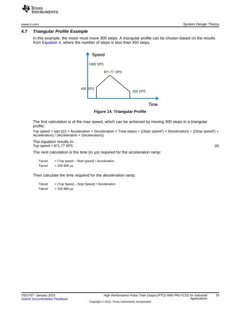
4.7 Triangular Profile ExampleIn this example, the motor must move 300 steps. A triangular profile can be chosen based on the resultsfrom Equation 4, where the number of steps is less than 450 steps.
Figure 14. Triangular Profile
The first calculation is of the max speed, which can be achieved by moving 300 steps in a triangularprofile:Top speed = sqrt (((2 × Acceleration × Deceleration × Total steps) + ((Start speed2) × Deceleration) + ((Stop speed2) ×Acceleration) / (Acceleration + Deceleration))
The equation results in:Top speed = 871.77 SPS (6)
The next calculation is the time (in µs) required for the acceleration ramp:
Taccel = (Top speed – Start speed) / AccelerationTaccel = 235 889 µs
Then calculate the time required for the deceleration ramp:
Tdecel = (Top Speed – Stop Speed) / DecelerationTdecel = 335 889 µs
15TIDU707–January 2015 High Performance Pulse Train Output (PTO) With PRU-ICSS for IndustrialApplicationsSubmit Documentation Feedback
Copyright © 2015, Texas Instruments Incorporated
System Design Theory www.ti.com
4.8 Descriptor List ExampleEach block entry of the 32-byte descriptor information block is described in this section for the triangularprofile example.
Block entry 1: Current block and next blockThe first entry of the 32-byte information is the block number. There is 12KB of shared memory, whichindicates there is a total of 384 descriptor blocks. The first block number is initialized as 0 and thenincremented by 32 for every new block of information written. The block pointer always points to thestarting address of the next block, which is the second block in this example.
Offset 0x00: 0x0000.0020
Block entry 2: Direction bit and speed valueThe second block entry consists of the speed value and direction bit, which are encoded into one 32-byteentry. Bit 31 specifies the direction of the movement. All remaining bits are used for the speed value.
The speed value is the start speed of each ramp. In the example of the triangular profile, where the firstpart is the acceleration ramp, the speed value is:
Speed value (1) = Start speed × Base multiplier= 20 000= 0x4E20
For the deceleration ramp, the speed value is:
Speed value (2) = Top speed × Base multiplier= 43 588= 0xAA44
For a trapezoidal profile, the speed value for the constant speed ramp and the deceleration ramp is:
Speed value = Max speed × Base multiplier= 50 000= 0xC350
The direction bit 31 is set as follows:
Bit 31 = ‘1’ → ForwardBit 31 = ‘0’ → Backward
The first descriptor entry for the example is configured as:
Offset 0x04: 0x8000.4E20 // FORWARD, 20000
Block entry 3: Acceleration valueThe next entry to be written is the acceleration value.
rAccel = Acceleration / GCD= 1
Offset 0x08: 0x0000.0001
16 High Performance Pulse Train Output (PTO) With PRU-ICSS for Industrial TIDU707–January 2015Applications Submit Documentation Feedback
Copyright © 2015, Texas Instruments Incorporated

www.ti.com System Design Theory
Block entry 4: Compare valueThe next entry is the compare value.
rCmp = Base multiplier × Pulse_position_raster= 500 000 000= 0x1DCD6500
Offset 0x0C: 0x1DCD6500
Block entry 5: Ramp timeThe next entry to be written is the ramp time. The value is in microseconds.
For the acceleration ramp, the time required to reach the top speed from the start speed is written.
Taccel = 235 889= 0x39971
For the deceleration ramp, the time required to reach the stop speed from the top speed is written.
Tdecel = 335 889= 0x52011
The first descriptor entry for the example is configured as:
Offset 0x10: 0x0003.9971
Block entry 6: Acc_type, Index, and Acc_divThe Acc_type, Index, and Acc_div are encoded into one entry.
The Acc_type and Index take 8 bits each and the 16 bits are provided for the Acc_div.
The Acc_div is a fixed-parameter:
Acc_div = 10= 0x000A
The acceleration type is 1 if it is an acceleration ramp, for deceleration it is 0:
Acc_type = 1 // acceleration for the first acceleration ramp= 0x000A
The Index is currently reserved and must be filled out with 0.
The first descriptor entry for the example is configured as:
Offset 0x14: 0x0100.000A
Block entry 7: Match valueThis entry is reserved and must be filled out with 0.
Offset 0x18: 0x0000.0000
17TIDU707–January 2015 High Performance Pulse Train Output (PTO) With PRU-ICSS for IndustrialApplicationsSubmit Documentation Feedback
Copyright © 2015, Texas Instruments Incorporated

System Design Theory www.ti.com
Block entry 8: Status, PTO pin 1, and PTO pin 2Bit 31 of the block entry defines the PRU stop condition. If this bit is set, the PRU stops the execution afterexecuting this block.
PTO pins 1 and 2 define the PRU general-purpose out pin numbers that are used for step and direction. Inthe TMDSICE3359 EVM example, the pin numbers are configured for R30[1] and R30[2].
The first descriptor entry for the example is configured as:
Offset 0x1C: 0x0000.0201
4.9 Shared Memory ConfigurationThe descriptor must be written by the ARM application. The previous calculated values fill out the sharedmemory descriptor list for the triangular profile as follows:
First descriptor
0x4A31.0000 0x0000.00200x4A31.0004 0x8000.4E200x4A31.0008 0x0000.00010x4A31.000C 0x1DCD.65000x4A31.0010 0x0003.99710x4A31.0014 0x0100.000A0x4A31.0018 0x0000.00000x4A31.001C 0x0000.0201
Second descriptor
0x4A31.0020 0x0020.00400x4A31.0024 0x8000.AA440x4A31.0028 0x0000.00010x4A31.001C 0x1DCD.65000x4A31.0030 0x0005.20110x4A31.0034 0x0000.000A0x4A31.0038 0x0000.00000x4A31.003C 0x8000.0201
18 High Performance Pulse Train Output (PTO) With PRU-ICSS for Industrial TIDU707–January 2015Applications Submit Documentation Feedback
Copyright © 2015, Texas Instruments Incorporated

www.ti.com Getting Started
5 Getting Started
5.1 OverviewThe following tools are required for the evaluation of the PTO firmware on the PRU-ICSS:• Personal computer (PC) with an installation of Code Composer Studio Version 6 (CCSv6)• PRU Compiler from the CCSv6 App Center• TMDSICE3359 ICE EVM with a USB cable connected to the PC that has CCSv6 installed
NOTE: The TMDSICE3359 EVM has an on-board JTAG support through the XDS100v2 JTAGemulator. For other TI development boards with Sitara processors and a PRU-ICSS, anadditional JTAG debugger may be required to connect the board via the JTAG to CCSv6. Ifsuch a JTAG connection exists, the PTO example can be evaluated with those boards, aswell.
5.2 PTO Firmware Load SequenceTo load the PRU firmware into the PRU-ICSS, the following steps must be performed.1. Connect the PC via USB cable to the ICE EVM. If connecting for the first time, this initiates the
installation of the JTAG over the USB driver for the EVM.2. In CCSv6, create a new Target Configuration file for the ICE EVM. Choose the appropriate .gel init file
for the TMDSICE3359. Check using the Test Connection button that the Target Configuration file setupis satisfactory.
3. Launch the Target Configuration file to connect through the JTAG to the TMDSICE3359 board.
19TIDU707–January 2015 High Performance Pulse Train Output (PTO) With PRU-ICSS for IndustrialApplicationsSubmit Documentation Feedback
Copyright © 2015, Texas Instruments Incorporated

Getting Started www.ti.com
4. In the Debug window, connect to the Cortex A8 processor; if required, send theAM3359_ICE_Initializiation .gel script. This script initializes the AM335x on the TMDSICE3359 board.
5. Load the additional .gel files to enable initialization of the PRU-ICSS and PTO functions.
6. With the Cortex_A8 still selected in the Debug window, send the PRU_ICSS_init, PTO_Pinmux, andthe PTO_WriteExamplePTODescriptorToSharedMemory .gel scripts.
7. Select and connect to PRU_0 in the Debug window.
20 High Performance Pulse Train Output (PTO) With PRU-ICSS for Industrial TIDU707–January 2015Applications Submit Documentation Feedback
Copyright © 2015, Texas Instruments Incorporated

www.ti.com Getting Started
8. Load the PRU program into PRU_0.
9. Revisit the shared memory location at 0x1.0000 via the Memory Browser window and check the PTOdescriptor list. Modify as needed.
10. Run the program. The output can be observed with a scope connected to the PTO pins.
5.3 PTO .gel Script Additions
5.3.1 PRU-ICSS Init .gel ScriptAfter the power cycle, the PRU-ICSS is in power-down mode. The PRU-ICSS must be enabled by theARM before CCS can connect the PRU. The .gel script used to enable the PRU-ICSS is located on theBeagleBoard GitHub website: https://github.com/beagleboard/am335x_pru_package.
Please follow the instructions provided on the GitHub website to add the AM335x_PRU_ICSS.gel into theCCS project. The GitHub website offers a tutorial CCS_PRU_Debugger-training.pdf to provide furtherinformation on how to use the PRU with CCS.
21TIDU707–January 2015 High Performance Pulse Train Output (PTO) With PRU-ICSS for IndustrialApplicationsSubmit Documentation Feedback
Copyright © 2015, Texas Instruments Incorporated

Getting Started www.ti.com
5.3.2 Pinmux Configuration .gel ScriptThe appropriate pin-multiplexing (pinmux) must be applied to the board in order to access the PTO pinson the TMDSICE3359 board. This example uses the register mapped GPO at R30[14] and R30[15] of thePRU0.
The .gel example configures the pinmux and sets up an example descriptor list in the shared memory.TI™ recommends creating a new .gel file (for example, PTO.gel) that includes the following .gel textexample.
menuitem "PTO with PRU_ICSS"hotmenu PTO_Pinmux(){
*((unsigned int*) (0x44E10000 + 0x830)) = 0xE; // pr1_pru0_pru_r30_14 (mode 6),pullup/pulldown disabled
*((unsigned int*) (0x44E10000 + 0x834)) = 0xE; // pr1_pru0_pru_r30_14 (mode 6),pullup/pulldown disabled}
hotmenu PTO_WriteExamplePTODescriptorToSharedMemory(){
// First descriptor*((unsigned int*) (0x4A310000 + 0x00)) = 0x00000020;*((unsigned int*) (0x4A310000 + 0x04)) = 0x80004E20;*((unsigned int*) (0x4A310000 + 0x08)) = 0x00000001;*((unsigned int*) (0x4A310000 + 0x0C)) = 0x1DCD6500;*((unsigned int*) (0x4A310000 + 0x10)) = 0x00039971;*((unsigned int*) (0x4A310000 + 0x14)) = 0x0100000A;*((unsigned int*) (0x4A310000 + 0x18)) = 0x00000000;*((unsigned int*) (0x4A310000 + 0x1C)) = 0x00000201;
// Second descriptor*((unsigned int*) (0x4A310000 + 0x20)) = 0x00200040;*((unsigned int*) (0x4A310000 + 0x24)) = 0x8000AA44;*((unsigned int*) (0x4A310000 + 0x28)) = 0x00000001;*((unsigned int*) (0x4A310000 + 0x2C)) = 0x1DCD6500;*((unsigned int*) (0x4A310000 + 0x30)) = 0x00052011;*((unsigned int*) (0x4A310000 + 0x34)) = 0x0000000A;*((unsigned int*) (0x4A310000 + 0x38)) = 0x00000000;*((unsigned int*) (0x4A310000 + 0x3C)) = 0x80000201;
}
22 High Performance Pulse Train Output (PTO) With PRU-ICSS for Industrial TIDU707–January 2015Applications Submit Documentation Feedback
Copyright © 2015, Texas Instruments Incorporated

^]����¡��D335x processor
ARMARM
Industrial Application
PTO Control
PRU-ICSS Subsystem
Shared Memory
PRU
Tektronix MSO5104
Mixed Signal Oscilloscope
www.ti.com Test Setup
6 Test SetupThe PTO output pin of the TMDSICE3359 EVM is connected to the Tektronix MSO5105 Mixed SignalOscilloscope.
7 Test Data
7.1 Jitter MeasurementThe test is performed with the integrated histogram test feature of the Tektronix MSO5104 Mixed SignalOscilloscope.
The jitter measurement test is performed with the following parameters:
1 MHz• PTO frequency:500 000 000• Compare value:50 000 000• Speed value:222 500• Population:
23TIDU707–January 2015 High Performance Pulse Train Output (PTO) With PRU-ICSS for IndustrialApplicationsSubmit Documentation Feedback
Copyright © 2015, Texas Instruments Incorporated

Test Data www.ti.com
The histogram chart (right window) in Figure 15 shows that the maximum expected jitter of 50 ns at themaximum PTO frequency is not crossed. Most hits are at 1 µs and the deviation is never more than 50 ns.
Figure 15. Oscilloscope Image
24 High Performance Pulse Train Output (PTO) With PRU-ICSS for Industrial TIDU707–January 2015Applications Submit Documentation Feedback
Copyright © 2015, Texas Instruments Incorporated

www.ti.com Design Files
8 Design Files
8.1 SchematicsTo download the schematics, see the design files at TIDEP0027.
8.2 BOMTo download the bill of materials (BOM), see the design files at TIDEP0027.
8.3 PCB LayoutTo download the layer plots, see the design files at TIDEP0027.
9 Software FilesTo download the software files for the TIDEP0027 reference design, visit the TI website athttp://www.ti.com/tool/tidep0027.
10 References
1. Texas Instruments, AM3359 Industrial Communications Engine,TMDSICE3359 EVM, (TMDSICE3359).2. EE Times-India, Generate stepper-motor speed profiles in real time, David Austin,
http://fab.cba.mit.edu/classes/MIT/961.09/projects/i0/Stepper_Motor_Speed_Profile.pdf.3. GitHub, BeagleBone PRU Package on Github, https://github.com/beagleboard/am335x_pru_package.4. Code Composer Studio Download page, http://processors.wiki.ti.com/index.php/Download_CCS.
11 TerminologyASIC— Application Specific Integrated Circuit
CCS— Code Composer Studio
GPO— General Purpose Output
ICSS— Industrial Communication Subsystem
FPGA— Field Programmable Gate Array
PLC— Programmable Logic Controller
PRU— Programmable Real-time Unit
PTO— Pulse Train Output
25TIDU707–January 2015 High Performance Pulse Train Output (PTO) With PRU-ICSS for IndustrialApplicationsSubmit Documentation Feedback
Copyright © 2015, Texas Instruments Incorporated

About the Author www.ti.com
12 About the AuthorTHOMAS MAUER is a System Applications Engineer in the Factory Automation and Control Team atTexas Instruments Freising, where he is responsible for developing reference design solutions for theindustrial segment. Thomas brings to this role his extensive experience in industrial communications likeIndustrial Ethernet and fieldbuses and industrial applications. Thomas earned his Electrical Engineeringdegree (Dipl. Ing. (FH)) at the University of Applied Sciences in Wiesbaden, Germany.
GANESH MOHAN NELLIPARAMBIL is a Master Intern (Control and Embedded Instrumentation atESIGELEC in Rouen, France and in Embedded Systems and Instrumentation at Manipal University inManipal, India) in the Factory Automation and Control Team at Texas Instruments Freising, where he isresponsible for developing reference design solutions for the industrial segment. Ganesh earned hisBachelor’s degree in Instrumentation and Control Engineering from Anna University in Chennai, India.
INGOLF FRANK is a Systems Engineer in the Texas Instruments Factory Automation and Control team,focusing on programmable logic controller I/O modules. Ingolf works across multiple product families andtechnologies to leverage the best solutions possible for system level application design. Ingolf earned hisElectrical Engineering degree (Dipl. Ing. (FH)) in the field of information technology at the University ofApplied Sciences Bielefeld, Germany in 1991.
26 High Performance Pulse Train Output (PTO) With PRU-ICSS for Industrial TIDU707–January 2015Applications Submit Documentation Feedback
Copyright © 2015, Texas Instruments Incorporated

IMPORTANT NOTICE FOR TI REFERENCE DESIGNS
Texas Instruments Incorporated ("TI") reference designs are solely intended to assist designers (“Buyers”) who are developing systems thatincorporate TI semiconductor products (also referred to herein as “components”). Buyer understands and agrees that Buyer remainsresponsible for using its independent analysis, evaluation and judgment in designing Buyer’s systems and products.TI reference designs have been created using standard laboratory conditions and engineering practices. TI has not conducted anytesting other than that specifically described in the published documentation for a particular reference design. TI may makecorrections, enhancements, improvements and other changes to its reference designs.Buyers are authorized to use TI reference designs with the TI component(s) identified in each particular reference design and to modify thereference design in the development of their end products. HOWEVER, NO OTHER LICENSE, EXPRESS OR IMPLIED, BY ESTOPPELOR OTHERWISE TO ANY OTHER TI INTELLECTUAL PROPERTY RIGHT, AND NO LICENSE TO ANY THIRD PARTY TECHNOLOGYOR INTELLECTUAL PROPERTY RIGHT, IS GRANTED HEREIN, including but not limited to any patent right, copyright, mask work right,or other intellectual property right relating to any combination, machine, or process in which TI components or services are used.Information published by TI regarding third-party products or services does not constitute a license to use such products or services, or awarranty or endorsement thereof. Use of such information may require a license from a third party under the patents or other intellectualproperty of the third party, or a license from TI under the patents or other intellectual property of TI.TI REFERENCE DESIGNS ARE PROVIDED "AS IS". TI MAKES NO WARRANTIES OR REPRESENTATIONS WITH REGARD TO THEREFERENCE DESIGNS OR USE OF THE REFERENCE DESIGNS, EXPRESS, IMPLIED OR STATUTORY, INCLUDING ACCURACY ORCOMPLETENESS. TI DISCLAIMS ANY WARRANTY OF TITLE AND ANY IMPLIED WARRANTIES OF MERCHANTABILITY, FITNESSFOR A PARTICULAR PURPOSE, QUIET ENJOYMENT, QUIET POSSESSION, AND NON-INFRINGEMENT OF ANY THIRD PARTYINTELLECTUAL PROPERTY RIGHTS WITH REGARD TO TI REFERENCE DESIGNS OR USE THEREOF. TI SHALL NOT BE LIABLEFOR AND SHALL NOT DEFEND OR INDEMNIFY BUYERS AGAINST ANY THIRD PARTY INFRINGEMENT CLAIM THAT RELATES TOOR IS BASED ON A COMBINATION OF COMPONENTS PROVIDED IN A TI REFERENCE DESIGN. IN NO EVENT SHALL TI BELIABLE FOR ANY ACTUAL, SPECIAL, INCIDENTAL, CONSEQUENTIAL OR INDIRECT DAMAGES, HOWEVER CAUSED, ON ANYTHEORY OF LIABILITY AND WHETHER OR NOT TI HAS BEEN ADVISED OF THE POSSIBILITY OF SUCH DAMAGES, ARISING INANY WAY OUT OF TI REFERENCE DESIGNS OR BUYER’S USE OF TI REFERENCE DESIGNS.TI reserves the right to make corrections, enhancements, improvements and other changes to its semiconductor products and services perJESD46, latest issue, and to discontinue any product or service per JESD48, latest issue. Buyers should obtain the latest relevantinformation before placing orders and should verify that such information is current and complete. All semiconductor products are soldsubject to TI’s terms and conditions of sale supplied at the time of order acknowledgment.TI warrants performance of its components to the specifications applicable at the time of sale, in accordance with the warranty in TI’s termsand conditions of sale of semiconductor products. Testing and other quality control techniques for TI components are used to the extent TIdeems necessary to support this warranty. Except where mandated by applicable law, testing of all parameters of each component is notnecessarily performed.TI assumes no liability for applications assistance or the design of Buyers’ products. Buyers are responsible for their products andapplications using TI components. To minimize the risks associated with Buyers’ products and applications, Buyers should provideadequate design and operating safeguards.Reproduction of significant portions of TI information in TI data books, data sheets or reference designs is permissible only if reproduction iswithout alteration and is accompanied by all associated warranties, conditions, limitations, and notices. TI is not responsible or liable forsuch altered documentation. Information of third parties may be subject to additional restrictions.Buyer acknowledges and agrees that it is solely responsible for compliance with all legal, regulatory and safety-related requirementsconcerning its products, and any use of TI components in its applications, notwithstanding any applications-related information or supportthat may be provided by TI. Buyer represents and agrees that it has all the necessary expertise to create and implement safeguards thatanticipate dangerous failures, monitor failures and their consequences, lessen the likelihood of dangerous failures and take appropriateremedial actions. Buyer will fully indemnify TI and its representatives against any damages arising out of the use of any TI components inBuyer’s safety-critical applications.In some cases, TI components may be promoted specifically to facilitate safety-related applications. With such components, TI’s goal is tohelp enable customers to design and create their own end-product solutions that meet applicable functional safety standards andrequirements. Nonetheless, such components are subject to these terms.No TI components are authorized for use in FDA Class III (or similar life-critical medical equipment) unless authorized officers of the partieshave executed an agreement specifically governing such use.Only those TI components that TI has specifically designated as military grade or “enhanced plastic” are designed and intended for use inmilitary/aerospace applications or environments. Buyer acknowledges and agrees that any military or aerospace use of TI components thathave not been so designated is solely at Buyer's risk, and Buyer is solely responsible for compliance with all legal and regulatoryrequirements in connection with such use.TI has specifically designated certain components as meeting ISO/TS16949 requirements, mainly for automotive use. In any case of use ofnon-designated products, TI will not be responsible for any failure to meet ISO/TS16949.IMPORTANT NOTICE
Mailing Address: Texas Instruments, Post Office Box 655303, Dallas, Texas 75265Copyright © 2015, Texas Instruments Incorporated