anywave technical seminar july 2016 ofdm isdb-t2
TRANSCRIPT

1
COMMUNICATION TECHNOLOGIES CO. LTD
Anywave Technical Presentation July 2016 – Focus on OFDM and ISDBT

2
ANYWAVE Agenda1. A Brief Overview Of ISDB-Tb Standards
2. Transmission System Basics
3. Transmitter Design
4. Advances In Solid State Technology
5. ISDB-T Transmitter Measurements
6. Safety And The Basics Of Transmitter Maintenance
7. OCR and Single Frequency Network (SFN)

3
1. A Brief Overview Of ISDB-T
ANYWAVE
ANYWAVE Presentation

4
HD ENCODER
SD ENCODER
1 SEG ENCODER
REMULTIPLEXER
EXTERNAL GPS
ISDBT TRANSMITTER
HD-SDI ~ 1.5GB/sSD-SDI ~ 270MB/s
300KB/s
3MB/s
15MB/s
~ 32.5MB/s RF ON CHANNEL
ANYWAVE ISDB-T Overview
SYSTEM CONFIGURATION

5
MPEG-4 VIDEO CODEC
MPEG-4 AAC AUDIO CODEC
AUDIO PACKET
VIDEO
SOUND
VIDEO PACKET
• The Audio and Video signals are converted to SDI signal
• The SDI is coded and compressed in MPEG-4 becoming a transport Stream (TS).
• The TS packet has 188 Bytes made up of the HEADER and PAYLOAD.
ANYWAVE ISDB-T Overview
SYSTEM CONFIGURATION

6
SYNCBYTE
8
TRANSPORTERROR
INDICATOR1
STARTINDICATOR
1
TRANSPORTPRIORITY
1
PID
13
SCRAMBLINGCONTROL
2
ADAPTIONCONTROL
2
CONTINUITYCONTROL
4
ADAPTIONFIELD
PAYLOAD
ANYWAVE ISDB-T Overview

7
THE ACRONYMS YOU SHOULD KNOW…
PSI/SI tables are responsible for the transmission of system and service information.
The main SI tables are: PAT, PMT, NIT, TOT and SDT.
• PAT – Program Association Table – Lists the PMT's present in the (TS)
• PMT – Program Map Table – Lists all PID's present in each service
• NIT – Network Information Table – Contains network info (Ex.: Station name, Station Id, etc...)
• TOT – Time Offset Table – Contains information related to time
• SDT – Service Description Table – Describes the services present in the TS
ANYWAVE ISDB-T Overview
8
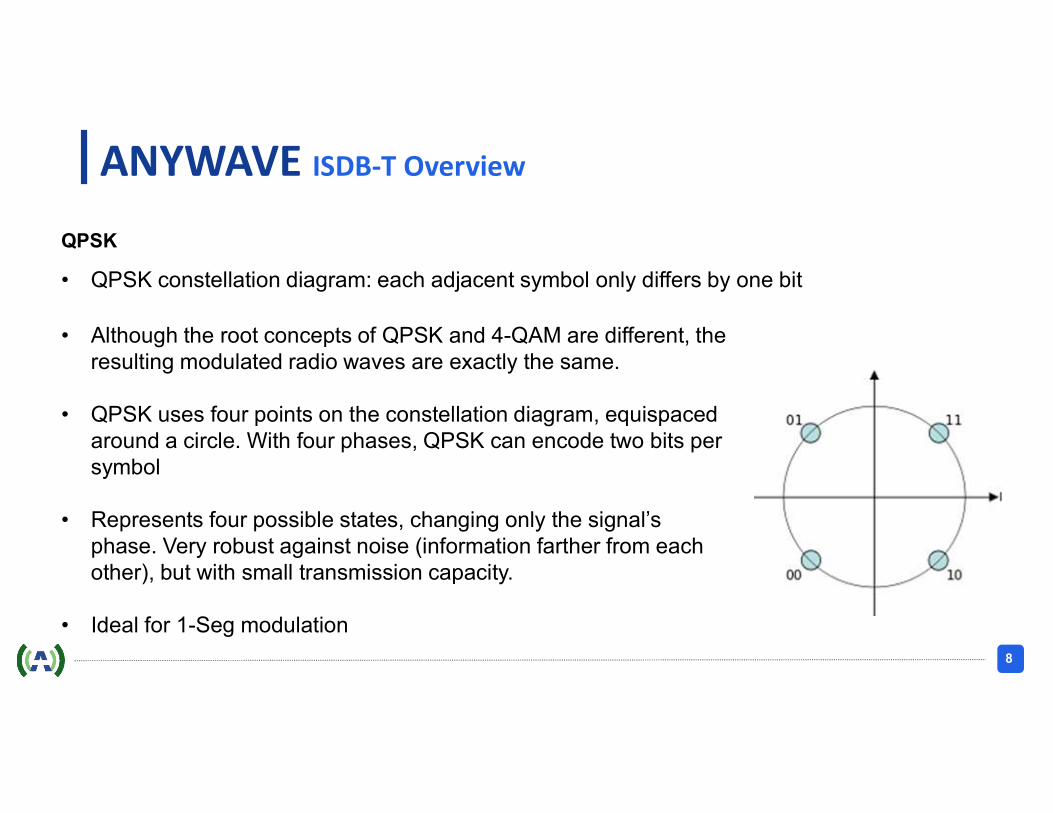
• Although the root concepts of QPSK and 4-QAM are different, the resulting modulated radio waves are exactly the same.
• QPSK uses four points on the constellation diagram, equispaced around a circle. With four phases, QPSK can encode two bits per symbol
• Represents four possible states, changing only the signal’s phase. Very robust against noise (information farther from each other), but with small transmission capacity.
• Ideal for 1-Seg modulation
• QPSK constellation diagram: each adjacent symbol only differs by one bit
ANYWAVE ISDB-T Overview
QPSK

9
• QAM is both an analog and a digital modulation scheme; and represents 16 possible states
• It conveys two digital bit streams, by changing (modulating) the amplitudes of two carrier waves, using the amplitude-shift keying (ASK) digital modulation scheme.
• The two carrier waves are out of phase with each other by 90° and are thus called quadrature carriers
• The modulated waves are summed, and the resulting waveform is a combination of both phase-shift keying (PSK) and amplitude-shift keying (ASK)
• Ideal for SD modulation
ANYWAVE ISDB-T Overview
16QAM

10
• 64-QAM Modulation Represents 64 possible states both changing phase and amplitude.
• Low strength signal but capable of high transmission rates.
• Ideal for HD
ANYWAVE ISDB-T Overview
64QAM

11
• FEC is the main component to burst noise immunity
• Guarantees the error correction for transmitted signals in the reception stage by simply adding redundancy bits.
• FEC can be adjusted to 1/2, 2/3, 3/4, 5/6 or 7/8.
• These numbers represent how many of the duplicated bits will be used. The higher the redundancy the higher is the immunity to burst noise, but the lower the transmission rate.
ANYWAVE ISDB-T Overview
FORWARD ERROR CORRECTION

12
• Guard Interval is responsible for multipath immunity;
• In analog what used to generate “ghosts”
• The size of this sample can be 1/4, 1/8, 1/16 or 1/32 of the symbol’s time.
• 1/4 – Greater multipath immunity but with less transmission capacity. 25% of the symbol is repeated.
• 1/32 – Less multipath immunity but with greater transmission capacity. Only 3.125% of the he symbol is repeated.
• The sample size influences the multipath immunity and the effective data transmission rate.
The OFDM symbol has its end part replicated at the beginning.ANYWAVE ISDB-T Overview
GUARD INTERVAL
13
MODE
• Defines the number of OFDM carriers that make up the 6 MHz channel.
• It has no influence on the transmission rate; only in multipath immunity (the longer the symbol the better) and in the Doppler effect in mobile reception (more space between carriers, or the smaller the symbol, the better).
• Mode 8k proved itself to be adequate for all types of transmission and is normally used in ISDB-TB transmissions.
ANYWAVE ISDB-T Overview

14
Multipath interference(frequency selective) Flat fading or impulse noise
After De-interleaving2-dimensional random errorSuitable for Viterbi and Reed Solomon error correction
Corrected Output (No errors)
ANYWAVE ISDB-T Overview
INTERLEAVING

15
HIERARCHICAL MODULATION
Hierarchical Modulation is obtained by changing the modulation and error correction parameters
Modulation type : QPSK, 16QAM, 64 QAM or DQPSK
Error Correction: Coding rate of convolutional code (1/2 – 7/8)
ANYWAVE ISDB-T Overview

16
ANYWAVE ISDB-T Overview
HDTV
SDTV
MOBILE

17
SUMMARY
ISDB-T Is a very robust transmission system due to:• Hierarchical modulation, • OFDM and• Variable Guard Interval• Time and frequency interleaving
Uses of MPEG4 encoding which decreases complexity and cost and offers SD, HDTV and ONE-SEG (mobile)
Capable of being received by mobile and fixed reception
THE GOOD NEWS.. With ISDB-T … You have the tools to get the job done… - Good coverage with plenty of options for HD, SD and mobile
ANYWAVE ISDB-T Overview

18
THANK YOU FOR YOUR ATTENTION
ANYWAVE
ANYWAVE COMMUNICATION TECHNOLOGIES CO. LTD
300 KNIGHTSBRIDGE PARKWAY,LINCOLNSHIRE, IL 60069-3655, USA

19
ANYWAVE for all your transmission needs

20
ANYWAVE
ANYWAVE COMMUNICATION TECHNOLOGIES CO. LTD
300 KNIGHTSBRIDGE PARKWAY,LINCOLNSHIRE, IL 60069-3655, USA
SEND US AN [email protected]
CALL US(+66) 83 618-9333
(+1) 847 415 2258 (Ext. 1)
VISIT OUR WEBSITEwww.anywavecom.com/en
For Product Inquiries, please don’t hesitate to contact us.

21
ANYWAVE Agenda1. A Brief Overview Of ISDB-Tb Standards
2. Transmission System Basics
3. Transmitter Design
4. Advances In Solid State Technology
5. ISDB-T Transmitter Measurements
6. Safety And The Basics Of Transmitter Maintenance
7. OCR and Single Frequency Network (SFN)
Anywave BTSI Presentation July 2016

22
2. Transmission System Basics
ANYWAVE
ANYWAVE Presentation

23
ANYWAVE Transmission System Basics
A Transmission System design has to consider the following:
• Transmitter Power Output (TPO)• Transmission Line Efficiency• Antenna Gain• Effective Radiating Power (ERP)• Total System Price

24
ANYWAVE Transmission System Basics
Two design methods:
• Fixed TPO• Objective ERP
With Fixed TPO
1. Select TPO to meet objective ERP2. Select type of antenna3. Select transmission line length and size
With Objective ERP
1. Select ERP2. Select type of antenna3. Select transmission line length and size

25
ANYWAVE Transmission System Basics
Select a transmitter Power Output:LPTV Range20, 100, 200, 400, 500W
MPTV Range1000, 1500, 2000, 2500W
HPTV 5kW to 20kW in 1kW steps

26
ANYWAVE Transmission System Basics
Type in Transmitter Power Output: 100, 200, 400, 800 ... etc.
Type in Channel (14-70)
Select Meters or Feet
Select Antenna typeChose Pattern if slot, choose number of panels and bays if Panel type.
Select transmission line size, type and length and if there is an additional horizontal run
For cost of OperationSelect Hours per Day and Average Cost of Electricity

27
ANYWAVE Transmission System Basics
ResultsERP = 3.595kW
Estimated Transmitter Consumption = 1.905KW
Estimated Cost of Operation
$1,390 / Year$116 / Month
Estimated Cost of Equipment Purchase
$37,900

28
ANYWAVE Transmission System Basics
Type in ERP Objective (5W – 1MW)
Type in Channel (14-70)
Select Meters or Feet
Select Antenna typeChose Pattern if slot, choose number of panels and bays if Panel type.
Select transmission line size, type and length and if there is an additional horizontal run
For cost of OperationSelect Hours per Day and Average Cost of Electricity

29
ANYWAVE Transmission System Basics
ResultsTPO = 1.1595kW
Estimated Transmitter Consumption = 3.408KW
Estimated Cost of Operation
$2,985 / Year$249 / Month
Estimated Cost of Equipment Purchase
$92,246

30
ANYWAVE Transmission System Basics
1650 3" SLOT $60,000
1750 2 1/4" SLOT $57,000
Selecting the right combination of Antenna type, Line size and TPO can realize significant savings.. In this case over $15,000.
TPO LINE SIZE ANT. TYPE PRICE
1650 3" SLOT $60,000
800 3" Panel $50,000
2100 1 5/8" SLOT $54,000
650 4" Panel $52,000
800 3" Panel $50,000
OBJECTIVE TO DELIVER 7KW ERP
1000 1 5/8" Panel $45,000

31
THANK YOU FOR YOUR ATTENTION
ANYWAVE
ANYWAVE COMMUNICATION TECHNOLOGIES CO. LTD
300 KNIGHTSBRIDGE PARKWAY,LINCOLNSHIRE, IL 60069-3655, USA

32
ANYWAVE for all your transmission needs

33
ANYWAVE
ANYWAVE COMMUNICATION TECHNOLOGIES CO. LTD
300 KNIGHTSBRIDGE PARKWAY,LINCOLNSHIRE, IL 60069-3655, USA
SEND US AN [email protected]
CALL US(+66) 83 618-9333
(+1) 847 415 2258 (Ext. 1)
VISIT OUR WEBSITEwww.anywavecom.com/en
For Product Inquiries, please don’t hesitate to contact us.

34
ANYWAVE Agenda1. A Brief Overview Of ISDB-Tb Standards
2. Transmission System Basics
3. Transmitter Design
4. Advances In Solid State Technology
5. ISDB-T Transmitter Measurements
6. Safety And The Basics Of Transmitter Maintenance
7. OCR and Single Frequency Network (SFN)
Anywave BTS Presentation July 2016

35
3. Transmitter Design
ANYWAVE
ANYWAVE Presentation

36
Criteria of developing a new Transmitter
• Its all about the MONEY!
From a manufacturers point of view• Lower manufacturing costs by using more effective and efficient methods, technology designs
and materials.• Include new features, benefits and concepts in order to be better than the rest
From the customers point of view• Lower capital costs• Lower Operational costs ; Efficiency, Maintenance, Spares and Repairs
ANYWAVE Transmitter Design

37
So how do we meet all these criterion?
• It’s all in the DESIGN
• If you make a transmitter reliable, you lower operating costs for the user and decrease support costs for the manufacturer.
• Reliability is about oversizing the materials, not cutting corners in materials and providing the appropriate protection for all scenarios
ANYWAVE Transmitter Design

38
ANYWAVE Transmitter Design
Carved ALUMINUM HEAT SINK
• Single Piece of Aluminum
• All BLF888 devices and reject loads are directly mounted onto heat sink for maximum heat dissipation and minimum heat transfer resistance
• Power cables are routed under the main board and within the carved heat sink.
AMPLIFIER DESIGN

39
ANYWAVE Transmitter Design
Carved ALUMINUM HEAT SINK
• High density, heavy duty
• Light weight
• Special fin structure provides large equivalent surface area
• High density fin panels create air flow “turbulence” for very fast heat removal
• RESULT: VERY COOL OPERATING TEMPERATURE OF ENTIRE AMPLIFIER
AMPLIFIER DESIGN

40
ANYWAVE Transmitter Design
AMPLIFIER DESIGN
COOLING
• Brushless, speed control fans
• 267 CFM rating for each fan(operates at <100CFM)
• Fan speeds displayed on control unit and via Web browser remote control
• Temperature controlled for optimum efficiency and extended life
• Easily field replaceable with two screws and plug in connectors
• RESULT: Amplifiers operate very quietly and reliably

41
ANYWAVE Transmitter Design
AMPLIFIER DESIGN RF OUTPUT
• Heavy duty 7-16 DIN output connector
• Connector rated at 1kW capable handling power
(45% over-rating)
• No tools required to connect or disconnect

42
ANYWAVE Transmitter Design
Power Supply
• HOT PLUGGABLE – FROM FRONT OF TRANSMITTER
• No tools required to remove power supply
• Heavy power capacity 4000W AC/DC power supplies
• Total 4000W capacity for 500W ISDBT output
• Fire and smoke resistant wiring
AMPLIFIER DESIGN

43
ANYWAVE Transmitter Design
• Well shielded multiple compartment design
• All-digital bias and measurement adjustment
• Dedicated micro controller in each PA module for local monitoring
• Real time and continuous measurements on current, voltage, bias on each BLF888 device temperature, forward power and reflected power levels
AMPLIFIER DESIGN

44
ANYWAVE Transmitter Design
• Comprehensive Graphical user interface for remote access
• Complete control and ALL information available
REMOTE CONTROL AND MONITORING

45
ANYWAVE Transmitter Design
• Complete monitoring and control functions
• Large 5” touch screen• 30W output power level• System Status displayed
• Forward power• Reflected power• Rejection power levels• Optional dBm, Wattage or
percentage display• VSWR
Driver Status display• Input level• Exciter presence and selection• Forward power reflected power, current, voltage.• Real time log• Amplifier mode status displayed• Forward power, reflected power current, voltage, temperature bias voltage• Fans Speed• Remote accessibility: (1) RS232, (2) RS485, (1) RJ45, Web interface
(Available on transmitters above 400W).
CONTROL AND MONITORING

46
ANYWAVE Transmitter Design
• Transport Stream Processing
• Modulation• Automatic Digital
Pre-correction• Digital to Analog
Conversion• Amplification –• -25 – 5dBmb
Pre-amplification +18dBPre-amplification 14dBSplitter -6dBFinal amplification +17dB Combiner +6dBOutput ~ 400W
DigitalExciter
RF Power Amplifier
DirectionalCoupler
TS1input
Band Pass filter10-20dB shoulder reductionInsertion Loss of 0.6dB
Band PassFilter
Feedback Samples for power metering
Directional Coupler Single Probe provides samples for pre-correction(non-linear and linear)
Functionality

47
ANYWAVE Transmitter Design
EXCITER FUNCTIONAL DESCRIPTION
Digital Inputs
Analog Inputs
Digital (IP) and analogremote management inputs
Reference inputs (GPS, 1PPS etc.)
SIGNAL FLOW
SYNCRONIZATION CONTROL FEEDBACK
DISPLAY and CONTROL FUNCTIONS

48
ANYWAVE Transmitter Design
Output is made up of Two microstrips L3 and Balun B1.
C1 – C9 used to match transistor Impedance to 50 ohm.
Inductor L5 and C17/C18 improve match at LF.
The length of the Balun B1 is 1/8 the central frequency of mid UHF frequency i.e. 550MHz.
Input is made up of Two microstrips L32 and Balun B2.
R1/R2 LF DampingC34/C35 RFDecoupling for the Balun
R3-R6 and C35/C37Provides damping function that helps improve stability
AMPLIFIER OPERATIONAL DESCRIPTION

49
ANYWAVE Transmitter DesignTRANSISTORDESIGNUPDATE
NOW
NOW
SOON
FUTURE
Non-DohertyBroadband

50
THANK YOU FOR YOUR ATTENTION
ANYWAVE
ANYWAVE COMMUNICATION TECHNOLOGIES CO. LTD
300 KNIGHTSBRIDGE PARKWAY,LINCOLNSHIRE, IL 60069-3655, USA

51
ANYWAVE for all your transmission needs

52
ANYWAVE
ANYWAVE COMMUNICATION TECHNOLOGIES CO. LTD
300 KNIGHTSBRIDGE PARKWAY,LINCOLNSHIRE, IL 60069-3655, USA
SEND US AN [email protected]
CALL US(+66) 83 618-9333
(+1) 847 415 2258 (Ext. 1)
VISIT OUR WEBSITEwww.anywavecom.com/en
For Product Inquiries, please don’t hesitate to contact us.

53
ANYWAVE Agenda1. A Brief Overview Of ISDB-Tb Standards
2. Transmission System Basics
3. Transmitter Design
4. Advances In Solid State Technology
5. ISDB-T Transmitter Measurements
6. Safety And The Basics Of Transmitter Maintenance
7. OCR and Single Frequency Network (SFN)
Anywave BTSI Presentation July 2016

54
4. Advances in Solid State Technology
ANYWAVE
ANYWAVE Presentation

5555
A Brief History Of Solid State Transmitter Efficiencies
ANYWAVE Advances in Solid State Technology

56
Introduction
• Generation 1 released in the late 80’s was inefficient and unreliable• Generation 2: Philips BLF861A and Motorola MRF372 (180 watt – 14dB Gain)
• Efficiency of 2nd Generation devices (digital operation) ~18%
• In 2008 came Generation 3 was introduced; the “50” volt LDMOS • This resulted in lower cost per watt and helped reduced the cost of much higher
power transmitters• Efficiency increased to ~ 25%• The BLF888A became the standard for all manufacturers• However, efficiency of these devices “stalled” at the 25% level
• Improvements could be made in other areas of the transmitter but most only saw very small improvements in efficiency
ANYWAVE Advances in Solid State Technology

5757
To compete with vacuum tubes at high power namely the MSDC-IOT which had efficiencies in excess of 50%... A much higher efficiency was needed:
Two new “ideas” to make solid state efficiency compete with the IOT…
• Drain Modulation (or Envelope Tracking)
• Doherty Modulation
Efficiency
ANYWAVE Advances in Solid State Technology

58
PA
V dc
ATSC Modulator
ASI
RF
Operates by modulating the DRAIN of a FET amplifier with the input signal so that the Power Supply voltage follows the level of the input signal. The amplifier operates near the high-efficiency saturation.
Drain Modulation via Envelope Tracking (DM/ET)
ANYWAVE Advances in Solid State Technology
Wasted Power
V dc
Resulting in a Drain Efficiency is about 25%

59
ATSC Modulator PA
V dc
ASI
RF
DC - DC Converter
Wasted Power
V dc1mS
Operates by modulating the DRAIN of a FET amplifier with the input signal so that the Power Supply voltage follows the level of the input signal. The amplifier operates near the high-efficiency saturation.
Drain Modulation via Envelope Tracking (DM/ET)
ANYWAVE Advances in Solid State Technology
Resulting in a Drain Efficiency is about 30%

60
Operates by modulating the DRAIN of a FET amplifier with the input signal so that the Power Supply voltage follows the level of the input signal. The amplifier operates near the high-efficiency saturation.
ATSC Modulator PA
V dc
ASI
RF
Envelope Detector
SupplyModulator
De
lay
Wasted Power
Drain Modulation via Envelope Tracking (DM/ET)
ANYWAVE Advances in Solid State Technology
Resulting in a Drain Efficiency is about 40-50%

61
Drain Modulation via Envelope Tracking (DM/ET)
Drain Efficiency• Now ~ 38%• Future ~ 40-50%• Theoretical maximum ~ 80%
• Sophisticated circuitry including DAC, Filter, I/Q detector and quadrature mixer required.
• Circuitry has to be included very near and on every amplifier, hence complexity increases with number of amplifiers.
• Significantly higher component count decreases the mean time between failure (MTBF).
• Not chosen by most manufacturers due to complexity and additional costs
ANYWAVE Advances in Solid State Technology

62
Doherty Modulation
A1
A2
RF Input
Carrier Amplifier Class AB (saturates at high power input)
Peak Amplifier Class C (Turns on at high power input)
ANYWAVE Advances in Solid State TechnologyParalleling two amplifiers devices; first operating in Class AB which amplifies the average power level, and the second operates in Class C amplifying just the peaks of the waveform. Output of two devices are combined with a matched transformer.

6363
• DOHERTY configuration improves linearity at the high power input by complementing the saturation of the carrier amplifier with the turn on characteristics of the peak amplifier
Doherty Modulation
• Originally designed by William Doherty of Bell Labs in 1934
• In 2008 NXP semiconductors (founded by Philips, now called Ampelon) released a transistor “optimized” for Doherty amplifier applications. It has since been improved and commonly available… Example BLF888
ANYWAVE Advances in Solid State Technology

6464
P out
P in
Saturation
Carrier Amplifier
Doherty Modulation
Peak Amplifier
The addition of the PEAK and CARRIER Amplifiers
“Turn on”
ANYWAVE Advances in Solid State Technology

6565
• Amplifier efficiency
• Now ~ 40%• Future ~ 40-50%• Theoretical maximum ~ 50-60%
• Simple to implement with current circuitry available
• Due to two different devices feeding same load, impedance matching section is required and hence is frequency dependent limiting broadband operation.
• Band-limiting output combiner/matching section can be configured to provide easy “Broadband” operation; thru’ simple interchangeable parts. The “D” and “E” versions are becoming more broadband overcoming this issue.
Doherty Modulation
ANYWAVE Advances in Solid State Technology

66
ANYWAVE Advances in Solid State Technology
Consumption – ISDB-T
10kW UHF
74kW Of Wasted Power
48kW Of Wasted Power
24kW Of Wasted Power

67
Doherty Class AB and Class C
Standard Dual Class AB
Average of 75.6 C
Operating Temperature
T1 = 62.9 CT2 = 54.6 C
T1 = 75.7 CT2 = 75.5 C
Drain Modulation via Envelope Tracking
T1 = 58.9 C
Average of 58.7 C
Average of 58.9 C
Reduces transistor operating
temperature by 23 C
ANYWAVE Advances in Solid State Technology

6868
Conclusion
Doherty Modulation is
• Easier to implement
• Does not reduce the reliability of the standard Fixed Drain (FD) Transmitter
• Reduces operating temperature of amplifier
• (Potentially increasing the reliability)
• Provides a large efficiency improvement
• (Tens of thousands of savings compared to FD)
• Offers the lowest cost transmitter
ANYWAVE Advances in Solid State Technology

6969
ANYWAVE Advances in Solid State Technology
MPTV Range1kW, 1.5kW, 2kW, 3kW
Non-Doherty : 2, 20, 100, 200
Doherty: 400, 600W
All available in both Doherty and
Non Doherty
LPTV Range2, 20, 100, 200, 400, 600
The Choice is yours….

70
ANYWAVE for all your transmission needs

71
THANK YOU FOR YOUR ATTENTION
ANYWAVE
ANYWAVE COMMUNICATION TECHNOLOGIES CO. LTD
300 KNIGHTSBRIDGE PARKWAY,LINCOLNSHIRE, IL 60069-3655, USA

72
ANYWAVE
ANYWAVE COMMUNICATION TECHNOLOGIES CO. LTD
300 KNIGHTSBRIDGE PARKWAY,LINCOLNSHIRE, IL 60069-3655, USA
SEND US AN [email protected]
CALL US(+66) 83 618-9333
(+1) 847 415 2258 (Ext. 1)
VISIT OUR WEBSITEwww.anywavecom.com/en
For Product Inquiries, please don’t hesitate to contact us.

73
ANYWAVE Agenda1. A Brief Overview Of ISDB-Tb Standards
2. Transmission System Basics
3. Transmitter Design
4. Advances In Solid State Technology
5. ISDB-T Transmitter Measurements
6. Safety And The Basics Of Transmitter Maintenance
7. OCR and Single Frequency Network (SFN)

74
5. ISDB-Tb Transmitter Measurements
ANYWAVE
ANYWAVE Presentation

75
ANYWAVE ISDBT-Tb Transmitter Measurements
What are the KEY Measurements for an ISDB-Tb Transmitter?
• POWER
• Modulation Error Ratio (MER)
• Intermodulation Distortion (IMD)
And if possible….
• Harmonics (Out of band)
• Bit Error Rate (BER)

76
ANYWAVE ISDBT-Tb Transmitter Measurements
INTRODUCTION
• Broadcasting transmitters are subject to particularly stringent standards with respect to broadcast signal quality
• Small faults can lead to service disruptions for many viewers
• A single instrument, such as the R&S® ETL TV analyzer* can perform all required ISDB-T transmitter measurements
* Instead of the ETL the ETC or ETH can be a lower cost option

77
ANYWAVE ISDBT-Tb Transmitter Measurements
Two ways of making measurements
• OPTION 1: With External Test equipment
OR
• OPTION 2: With Anywave built in measurement system and Power calculation system using Historic data and component manufacturers results

78
ANYWAVE ISDBT-Tb Transmitter Measurements
EXCITER/MODULATOR
ENCODER
TransportStream
• The R&S®ETL TS has a built TS generator. This feeds an ISDB-T-compliant MPEG-2 transport stream (TS) to the TS input on the ISDB-T transmitter.
• Or a compliant ISDB-T encoder can be used.
• Even without a Transport Stream source Output Power calibration and the measurements of MER, Shoulders can still be taken.

79
ANYWAVE ISDBT-Tb Transmitter Measurements
ENCODER
EXCITER/MODULATOR
RF AMPLIFIER
RF BAND PASSFILTER
RF DUMMY LOAD
TEST EQUIPMENTR&S® ETL
R&S® NRP
PC
DIRECTIONALCOUPLER “A”
TransportStream
RF On Channel
DIRECTIONALCOUPLER “B”
RF On Channel
OPTION 1

80
Orthogonal frequency division multiplex (OFDM) signals exhibit a very high crest factor because in extreme cases, all carriers could be overlaid or even eliminated at any given moment.
Where N = Number of carriers
ANYWAVE ISDBT-Tb Transmitter Measurements
It is important to know the crest factor so that the components that follow the transmitter – such as the mask filter, the antenna combiner, the coaxial cable and the antenna, can be sized adequately.
The crest factor (CF) defines the relationship between the highest occurring amplitude of the modulated carrier signal and the RMS voltage of a signal:
CF = 20 10
CF OFDM = 10 10 2
Crest Factor

81
ANYWAVE ISDBT-Tb Transmitter Measurements
• The (CCDF) complementary cumulative distribution function includes the statistical probability that a signal peak will occur.
• For ISDB-T, a theoretical value of > 40 dB results for mode III .
• In practice, it is limited to about 13 dB in the transmitter.
Crest Factor

82
ANYWAVE ISDBT-Tb Transmitter Measurements
0 2 4 6 8 10 12 14 16 18 20
10²
10
10ᴼ
10
1
-1
Instantaneous Power / Average Power Ratio
Pro
bab
ility
%
CF = ~ 13dB
4% at 10dB(4kW)
0.1% at 11.8dB7.6kW
Assume at TPO = 400WCrest Factor

83
ANYWAVE ISDBT-Tb Transmitter Measurements
Modulator Characteristics I/Q Imbalance
ISDB-T modulators are essentially an IFFT signal processing block followed by an I/Q modulator. This I/Q modulator can be either digital or analog. Anywave’s modulator is Digital. If an ISDB-T modulator uses direct modulation, then the I/Q modulator it must be aligned cleanly to minimize the following influencing factors:
● Amplitude imbalance ● Quadrature error ● Carrier suppression
It is difficult to measure these items without a spectrum analyzer, as poor carrier suppression is recognizable as a notch directly at mid band and results in a contorted and compressed constellation diagram in mid-band. Amplitude imbalance and quadrature error negatively affect the MER.
The Anywave modulator automatically corrects for minimum I/Q imbalance
84
ANYWAVE ISDBT-Tb Transmitter Measurements
Amplitude Frequency Response and Group Delay
• In analog television, amplitude frequency response and group delay were important parameters for a transmission path between the transmitter output and the receiver input.
• Because of the channel correction in the ISDB-T receiver, significantly larger tolerances can now be permitted without noticeable reductions in quality. The mask filter and antenna combiners cause linear distortions.
• These linear distortions can be compensated by a pre-corrector within the transmitter. As a result, however, the linear distortions appear reversed when measured at the transmitter output.
• Therefore, the preferred method is to measure amplitude frequency response and group delay after all filter stages.

85
ANYWAVE ISDBT-Tb Transmitter Measurements
Out-of-Band Emissions
There are THREE distinct components:
● Shoulder attenuationDescribes the power of the noise components close to the edge of the channel
● Adjacent channel emissions Components within several MHz of the channel boundaries
● Harmonics Components at multiples of the transmit frequency

86
ANYWAVE ISDBT-Tb Transmitter Measurements
Shoulder Attenuation and Adjacent Channel Emissions
• The mask filter is used to reduce these unwanted out-of-band emissions.
• Critical mask filters are used when an adjacent channel requires protection, making more stringent requirements for attenuation of out-of-band emissions necessary.
• The high dynamic range of the signal after the mask filter makes it impossible to check adherence to the tolerance mask directly using a spectrum analyzer. This is why an adjustable notch filter is typically used to reduce the useful band power.
• The correct method is a complicated process using a tracking generator and additional notch filters to attenuate the fundamental frequency so as not to overload the analyzer.

87
ANYWAVE ISDBT-Tb Transmitter Measurements
Harmonics
• In addition to adjacent channel emissions, multiples of the transmit frequency can also result in harmonics. A harmonic filter at the transmitter output is used to suppress these harmonics.
• The R&S®ETL TV analyzer can be used to measure out-of-band emissions in spectrum analyzer mode. Because the mask filter does not suppress these harmonics, but rather affects only the channel near range, the harmonics can be measured directly at transmitter output.
• The high dynamic range of the signal means that a suitable high pass filter must be used to attenuate the useful channel by at least 40 dB.
• Notch filters (which are coaxial cavity filters that can be manually adjusted to the channel being suppressed) are not suitable here because they do not attenuate in just the useful band, but rather are repeated at multiples of the useful band.

88
ANYWAVE ISDBT-Tb Transmitter Measurements
Frequency Accuracy
• Single-frequency networks (SFN), in particular, place very stringent requirements on the frequency accuracy of an ISDB-T transmitter of less than 10-9.
• The carrier frequency offset can be measured using the R&S®ETL in TV/radio analyzer/receiver mode or a very accurate frequency counter.

89
ANYWAVE ISDBT-Tb Transmitter Measurements
• Complex Modulation Error Ratio (Complex MER) is a complex form of the S/N measurement that is made by including Q (quadrature) channel information in the ideal and error signal power computations. MER is defined by the following formula:
∑
∑
Where
MER is the Modulation Error Ratio in dB
are the Ideal I-channel and Q-channel symbols.
∂ I j and ∂ Qj are the Errors between received and ideal I- channel and Q-channel symbols.

90
ANYWAVE ISDBT-Tb Transmitter Measurements
Modulation Error Ratio
• A high MER value indicates good signal quality.
• In practice, the MER is 20 to 42 dB.
• A good ISDB-T transmitter has a MER in the range of approximately 35-38 dB.
• When receiving ISDB-T signals over a roof antenna with gain, a MER of 20 dB to 30 dB would be measurable at the antenna port.
• Values between 13 dB and 20 dB are expected for portable receivers with a indoor antenna.
• The MER is the single most important quality parameter for an ISDB-T transmitter.

91
ANYWAVE ISDBT-Tb Transmitter Measurements
Constellation Diagram
• Good MER is indicated by small and concentrated dots
Bad MER, represented by scattered and distorted dots in the constellation.

92
ANYWAVE ISDBT-Tb Transmitter Measurements
Bit Error Ratio
• ISDB-T provides an outer and inner error correction in the form of Reed-Solomon (RS) block coding and convolutional coding, which are assessed using a Viterbi decoder. Both methods are capable of recognizing and correcting bit errors in the data stream.
• All interference of an ISDB-T transmission path can be expressed as bit error ratios (BER).
• In the case of a functional ISDB-T transmitter, only the BER before Viterbi can differ from null. It will lie in the range of 10–9 or less.

93
ANYWAVE ISDBT-Tb Transmitter Measurements
Phase Noise
• Can happen due to the local oscillator's instability
• In the OFDM modulation process, phase noise can cause a phase error in all of the sub-carriers at the same time.
• It causes the constellation dots to “twist” on their axis.
474 MHz 762 MHz 802 MHz
10 Hz 86.3 82.0 81.2
100 Hz 106.9 102.7 102.3
1 kHz 118.8 115.3 114.3
10 kHz 124.0 120.8 120.2
100 kHz 124.6 122.0 121.9
1 MHz 141.4 140.0 139.5

94
ANYWAVE ISDBT-Tb Transmitter Measurements
Phase Noise

95
Efficiency and Performance of Digital TV Transmitters
REF: Average Carrier Level
24dB
Un-corrected Class A-B Amplifier
ANYWAVE ISDBT-Tb Transmitter Measurements
IMD (Intermodulation Distortion) or Shoulders or Out of Band Mask

96
REF: Average Carrier Level
42dB
Corrected Class A-B Amplifier
ANYWAVE ISDBT-Tb Transmitter Measurements
IMD (Intermodulation Distortion) or Shoulders or Out of Band Mask

97
REF: Average Carrier Level
17dB
Un-corrected DOHERTY Amplifier
ANYWAVE ISDBT-Tb Transmitter Measurements
IMD (Intermodulation Distortion) or Shoulders or Out of Band Mask

98
REF: Average Carrier Level
39dB
Corrected DOHERTY Amplifier
ANYWAVE ISDBT-Tb Transmitter Measurements
IMD (Intermodulation Distortion) or Shoulders or Out of Band Mask

99
ANYWAVE ISDBT-Tb Transmitter Measurements
Testing an Anywave Transmitter with NO TEST EQUIPMENT
FREQ617M
AGCOFF
GPSNOGPS
1PPSERR
CTRLLCA
ADPCOFF
• Frequency is measured in the exciter.
• With a GPS connected you can be assured of the accuracy.

100
ANYWAVE ISDBT-Tb Transmitter Measurements
Testing an Anywave Transmitter with NO TEST EQUIPMENT
FWD100%
MER43.5
LIMD48
UIMD49
FREQ653M
Hz+00000
MODEMODE1
GI1/4
PROFF
A-B-C-13000
LAYA
RATE1/2
MAP16QAM
TI0
• Forward Power (+/- 3%)
• Modulation Error Ratio (+/- 1dB)
• Lower Intermodulation Distortion (+/- 1dB)
• Upper Intermodulation Distortion (+/- 1dB)
• On Channel Frequency
• Off Set Frequency
• Major status of modulation Modes: (GI, Layer, Rate, Modulation type and TI).

101
ANYWAVE ISDBT-Tb Transmitter Measurements
Testing an Anywave Transmitter with NO TEST EQUIPMENT
VOL_98.72
VOL_1212.07
VOL_5049.37
PA_FWD443.67
Power Calibration (Using the PAC Screen)
• The Forward Power will be calibrated at the factory on the designated frequency.
• If frequency is changed this calibration will not be correct.
To Re-calibrate the Forward Power
• The sum of the currents multiplied by the 50V level divided by the frequency/efficiency factor = the output power (+/-5%)
CUR1_ 5011.2
CUR2_5011.7
CUR3_5012.1
CUR4_5011.8

102
ANYWAVE ISDBT-Tb Transmitter Measurements
Testing an Anywave Transmitter with NO TEST EQUIPMENT
Filter PowerBand
CenterBand Edge Average Factor
100W 1.3 2.2 1.75 0.67
150W 1.0 2.0 1.50 0.71
250W 1.1 1.8 1.45 0.72
600W 1.2 1.6 1.4 0.72
1000W 0.8 1.4 1.10 0.78
1500W 0.6 1.1 0.85 0.82
1800W 0.6 1.1 0.85 0.82
2000W 0.6 1.1 0.85 0.82
3000W 0.6 1.1 0.85 0.82
7000W 0.6 1.1 0.85 0.82
Power Calibration
• Filters have a reasonably consistent attenuation over frequency
• The lower the power rating of the filter the higher the loss.
• Losses vary from 1.75dB to 0.6dB • Multiply amplifier output power by
FACTOR to obtain real TPO.

103
0.2
0.22
0.24
0.26
0.28
0.3
0.32
0.34
0.36
Efficiency Factor
ANYWAVE ISDBT-Tb Transmitter Measurements
Testing an Anywave Transmitter with NO TEST EQUIPMENT
200W (Two transistor) OFDM (DVB-T2 and ISDB-Tb)Example: Frequency 593MHz. Power Required 200W after the filter. Power factor at 593MHz = 0.28Filter loss is 0.72dB for a 250W filter. There are two transistors in aVOL_50 (50V PSU) = 49.87 CUR1_50 and CUR2_2 should read (ON AVERAGE)
200 / 0.28 / 49.87 / 0.72 / 2 = 9.95 AMPS i.e. 9.95 Amps* = 200W after filter output +/- 5%* Average of each transistor.

104
0.2
0.22
0.24
0.26
0.28
0.3
0.32
0.34
0.36
Efficiency Factor
ANYWAVE ISDBT-Tb Transmitter Measurements
Testing an Anywave Transmitter with NO TEST EQUIPMENT
400W (Four transistor) OFDM (DVB-T2 and ISDB-Tb)Example: Frequency 533MHz. Power Required 400W after the filter.VOL_50 (50V PSU) = 49.97 CUR1_50, CUR2_2, CUR3_50 and CUR4_50 should read (ON AVERAGE)
400 / 0.33 / 49.97 / .72 / 4 = 9.95 AMPS i.e. 8.42 Amps* = 400W after filter output +/- 5%* Average of each transistor.

105
0.2
0.22
0.24
0.26
0.28
0.3
0.32
0.34
0.36
Efficiency Factor
ANYWAVE ISDBT-Tb Transmitter Measurements
Testing an Anywave Transmitter with NO TEST EQUIPMENT
1500W (Six transistor, three amplifiers) OFDM (DVB-T2 and ISDB-Tb)Example: Frequency 497MHz. Power Required 1200W after the filter.VOL_50 (50V PSU) = 49.97 CUR1-6_50, should read (ON AVERAGE)
1200 / 0.35 / 49.97 / .82 / 6 / 3 = 4.65 AMPS i.e. 4.65 Amps* = 1200W after filter output +/- 5%* Average of each transistor.

106
ANYWAVE ISDBT-Tb Transmitter Measurements
Testing an Anywave Transmitter with NO TEST EQUIPMENT
Anywave will provide customer with a Frequency versus Power versus Transmitter software
Enter Frequency of operation,
Model number of transmitter
Power required
And the software will automatically tell you the currents of each transistor to reach that power.
The transmitter then can be calibrated very accurately at any frequency

107
ANYWAVE ISDBT-Tb Transmitter Measurements
Summary
• With Test Equipment make the following measurements regularly (one every six months)• POWER• Modulation Error Ratio (MER)• Bit Error Rate (BER) • Intermodulation Distortion (IMD)• Harmonics (Out of band emissions)
• Without Test Equipment• Transistor currents• MER• IMD

108
ANYWAVE for all your transmission needs

109
THANK YOU FOR YOUR ATTENTION
ANYWAVE
ANYWAVE COMMUNICATION TECHNOLOGIES CO. LTD
300 KNIGHTSBRIDGE PARKWAY,LINCOLNSHIRE, IL 60069-3655, USA

110
ANYWAVE
ANYWAVE COMMUNICATION TECHNOLOGIES CO. LTD
300 KNIGHTSBRIDGE PARKWAY,LINCOLNSHIRE, IL 60069-3655, USA
SEND US AN [email protected]
CALL US(+66) 83 618-9333
(+1) 847 415 2258 (Ext. 1)
VISIT OUR WEBSITEwww.anywavecom.com/en
For Product Inquiries, please don’t hesitate to contact us.

111
ANYWAVE Agenda1. A Brief Overview Of ISDB-Tb Standards
2. Transmission System Basics
3. Transmitter Design
4. Advances In Solid State Technology
5. ISDB-T Transmitter Measurements
6. Safety And The Basics Of Transmitter Maintenance
7. OCR and Single Frequency Network (SFN)

112
7. Safety and Maintenance
ANYWAVE
ANYWAVE Presentation

113
Safety• SAFETY FIRST. When appropriate wear goggles, take off your rings and watches, tuck in your shirt.• When working on “hot” equipment .. Keep you hand in your pocket• Don’t work when you are tired.• Don’t drive to the site too quickly• Try to work in teams
Inspection• Visual inspections can resolve most issues. Visual inspection should be
done with Power OFF. Useful tools .. Power flash light and mirror.
Reliability• Most RF systems are reliable.. It is usually the low voltage stuff that fails
first.• Most problems occur due to control circuits.. Know how the control system
works before there is a problem
ANYWAVE Safety and Maintenance

114
Environmental Conditions• A HOT and DIRTY transmitter is an unhappy transmitter!• Unhappy transmitters FAIL.• Try to keep the transmitter site as clean as possible. Clean the
transmitter floor, clean table tops regularly, and clean any air filters.• Make sure the room is air conditioned. Make sure the room
temperature does exceed 30 degrees C (85 F).
• Make sure there is plenty of air flow around the transmitter.
• A nice feature is to include a stand alone duct for the transmitter about 30 cms above the top of the transmitter. And let the hot air simply exhaust, a small exhaust fan can be included if the duct is longer than 3 meters.
ANYWAVE Safety and Maintenance

115
FWD100%
MER38.5
LIMD43.5
UIMD44.0
Forward Power0 – 100%
Upper Intermodulation Distortion (UIMD): 20 – 60dB
Modulation Error Ratio(MER) 25 – 50dB
Lower Intermodulation Distortion (LIMD): 20 – 60dB
POWER 100% = 0dB
Meter readings
ANYWAVE Safety and Maintenance

116
Grounding• The tower and incoming transmission line should be bonded
to the building lightning protective ground
• The Transmitter and electrical panel should be bonded to the building lightning protective ground
ANYWAVE Safety and Maintenance
Grounding RodsBelow Ground
Tower
Transmission Line
Transmitter Electrical Panel

117
• CHANGING CHANNEL
ANYWAVE Safety and Maintenance
• If your amplifier is Non-Doherty
• The process is simply
• Change the exciter frequency• Re-tune or replace the filter on the correct
channel…
• Re-calibrate the forward power.. Done!
• However, with a Doherty Hi-Efficiency amplifier… it is not so easy

118
• Hi-Efficiency Doherty Power Amplifiers based on the BLF 888B device provide high efficiencies (50% efficiency) but with narrow band operation
• The Anywave Doherty PA design has multiple sub-bands across UHF, and so re-tuning a Doherty PA involves replacing the three PA circuit boards (shown) with a circuit board that covers the desired channel frequency.
ANYWAVE Safety and Maintenance

119
• First remove the boards from the amplifier.
• To remove the board you must
• Access the power transistor board• Remove top amplifier panel• Remove inner shield cover
• Remove all the screws from the printed circuit board (about 40)
ANYWAVE Safety and Maintenance

120
• De-solder the power supply wires (2)
ANYWAVE Safety and Maintenance
• De-solder the transistors and combiners
(to be re-used)

121
• Replace the board with a new board of the correct sub-band
ANYWAVE Safety and Maintenance

122
ANYWAVE Safety and Maintenance
• Once the circuit boards are replaced, the power transistors and combiners are re-soldered into place
• All screws replaced
• Power supply wires re-soldered
• Apply AC power to amplifier

123
ANYWAVE Safety and Maintenance
• After the amplifier is now complete and ready to operate, the only thing left to do is re-bias the transistors to the correct level.
• This is accomplished by adjusting the potentiometers to the correct idle current (~0.5A). The idle current is monitored on the web interface via the RJ45 connector on the rear of the amplifier. There are two potentiometers per transistor (four total) for the board.

124
Summary
The key to success is
• Provide protected power• Thoroughly ground all equipment• Regularly check tightness of all connectors• Avoid using tools on RF connections less than 7/8” EIA flanges• Keep accurate records (initial snap shot of operation, then monthly)• Measure the SNR, IMD, Forward Power and Reflected power regularly (monthly)• Monitor PA device currents and temp – be sure do not reach max (monthly)• Keep the transmitter properly cooled• Keep the transmitter and the transmitter building clean• Don’t try to fix a working transmitter!
• SAFETY FIRST.. No one ever died because they could not watch your TV station !
ANYWAVE Safety and Maintenance

125
ANYWAVE for all your transmission needs

126
THANK YOU FOR YOUR ATTENTION
ANYWAVE
ANYWAVE COMMUNICATION TECHNOLOGIES CO. LTD
300 KNIGHTSBRIDGE PARKWAY,LINCOLNSHIRE, IL 60069-3655, USA

127
ANYWAVE
ANYWAVE COMMUNICATION TECHNOLOGIES CO. LTD
300 KNIGHTSBRIDGE PARKWAY,LINCOLNSHIRE, IL 60069-3655, USA
SEND US AN [email protected]
CALL US(+66) 83 618-9333
(+1) 847 415 2258 (Ext. 1)
VISIT OUR WEBSITEwww.anywavecom.com/en
For Product Inquiries, please don’t hesitate to contact us.

128
ANYWAVE Agenda1. A Brief Overview Of ISDB-Tb Standards
2. Transmission System Basics
3. Transmitter Design
4. Advances In Solid State Technology
5. ISDB-T Transmitter Measurements
6. Safety And The Basics Of Transmitter Maintenance
7. OCR and Single Frequency Network (SFN)

129
7. OCDR and SFN’s
ANYWAVE
ANYWAVE Presentation

130
What is an OCR and a Translator
130
OCR: Process the input signal by eliminating the “echo”, boost it and re-send it at the same frequency as the received frequency
Translator: Usually perform demodulation and decode to the received signal, and can be re-send at any frequency desired
ANYWAVE OCDR and SFN

131
• OCR uses the same frequency for re-transmitting (fin=fout)
• When the processing delay of OCR is much smaller than the guard interval, the re-transmitted signal and the original signal can form a SFN
• OCR is one of the most popular way to set up SFN
• Disadvantage of OCR• The transmitted power is limited by the “echo”• The quality of transmitted signal is easily deteriorated and can be a interference to other
tower
• Advantage of OCR• Doesn’t require additional transmit network• Easier installation and lower cost• Doesn’t require GPS as reference signal13
1
Interference Cancelling can overcome the disadvantage of OCR!
ANYWAVE OCDR and SFN
OCR and Single Frequency Network (SFN)

132
Echo Interference in OCR
Conclusion: The system gain of OCR is severely limited by the system isolation. Therefore how to increase the isolation is the key to OCR application!
G: System Gain
E: System Isolation
H: System transfer function
ANYWAVE OCDR and SFN

133
Interference Cancellation System (ICS)
ANYWAVE OCDR and SFN
Z is the phase relationship between the input and the output

134
Echo Types
1: Direct coupling between receiving antenna and transmitting antenna
2: Reflection of far-away mountain3: Reflection of nearby building4: Reflection of moving object
ANYWAVE OCDR and SFN

135
Echo Cancellation
ANYWAVE OCDR and SFN

136
Echo Cancellation in SFN
ANYWAVE OCDR and SFN

137
Concepts in Echo Cancellation
Signal Length: Length of received signal channel impulse response
ANYWAVE OCDR and SFN
Echo Delay: The delay between echo and received signal
Echo Window: Length of echo channel impulse response
Process Delay: The delay of echo cancellation process

138
OCR System Gain Example (w/o ICS)
ANYWAVE OCDR and SFN
Assume:
Received signal level:-50dBm
Antenna isolation:80dB
Conclusion:
Max system gain: Antenna isolation- 10dB = 70dB
Max transmitted power: Received signal power + max system gain= -50 + 70 = 20dBm

139
ANYWAVE OCDR and SFN
Assume:
Received signal level:-50dBm
Antenna isolation:80dB
Conclusion:
Max system gain: Antenna isolation- 10dB +30dB= 100dB
Max transmitted power: Received signal power + max system gain= -50 + 100 = 50dBm
OCR System Gain Example (with ICS)

140
Key Spec in ICS
Echo-to-Signal-Ratio
But most of all…
MER!!!!
ANYWAVE OCDR and SFN

141
Echo-to-Signal-Ratio
ANYWAVE OCDR and SFN

142
Reasons of MER Deterioration
• The MER of received signal
• The linear and non-linear distortion of the transmitted system
• Echo Ratio
ANYWAVE OCDR and SFN

143
Anywave Gap Filler with ICS
EOCR8000
PA100W
PA20W
PA200/400W
ANYWAVE OCDR and SFN

144
Anywave OCR Features (1)
• Auto Shutdown/Turn ON Function:• When the main transmitted tower shuts down for maintenance, our OCR will shut down
automatically; when the main tower resumes transmitting signal, our OCR will turn on automatically. No manual intervention is required.
• Signal Quality Auto Detection:• When the received signal quality, echo level or re-transmitted signal quality has
changed, our OCR will adjust its transmitted signal level automatically. If transmitted signal cannot meet broadcasting requirement after the adjustment, the OCR will shut down its output automatically. No manual intervention is required.
ANYWAVE OCDR and SFN
• Patented AECTM (Adaptive Echo Cancellation) technology continuously, automatically, and adaptively eliminates dynamically varying echoes from the received signal, providing easy installation, reducing engineering cost, and producing stable operation as well as excellent performance

145
Anywave Features continued
ANYWAVE OCDR and SFN
Echo Cancellation Mode• Echo Cancellation:30 dB (typical value)• Echo Time Range:≤ 4 μs• MER Loss• 0 dB Echo: MER Loss ≤ 3 dB or MER ≥ 26 dB (depends on main signal SNR)
• 10 dB Echo: MER Loss ≤ 5 dB or • MER ≥ 26 dB (depends on main signal SNR)
• Echo Time Range:≤ 4 μs• Processing Delay:≤ 10 μs (including ICS and DPD)

146
Anywave Features continued
• Supports current digital and mobile TV standards including DTMB, CMMB, DVB-T/H, DVB-T2, ISDB-T, ATSC, and ATSC-MH
• Patented AECTM (Adaptive Echo Cancellation) technology eliminates dynamically varying echoes
• Powerful ADPCTM (Adaptive Digital Pre-Correction) provides superior digital correction of all linear and non-linear
• Accurate ESSI (Echo Signal Strength Indicator) and RSSI (Received Signal Strength Indicator) functions provide direct field signal condition assessment and easy installation
• Digital ALC (Automatic Level Control) function supports wide RF input range and eliminates the LNA module
• Powerful anti-interference of adjacent channel
ANYWAVE OCDR and SFN

147
Application 1
Directional Reception and Omni Transmit in city
Transmitted Power Level:100WReceived Signal:-50dBmReceived MER= 25.2dBRe-Transmitted Signal MER=23.5dBEcho Ratio= 9dB
ANYWAVE OCDR and SFN
148
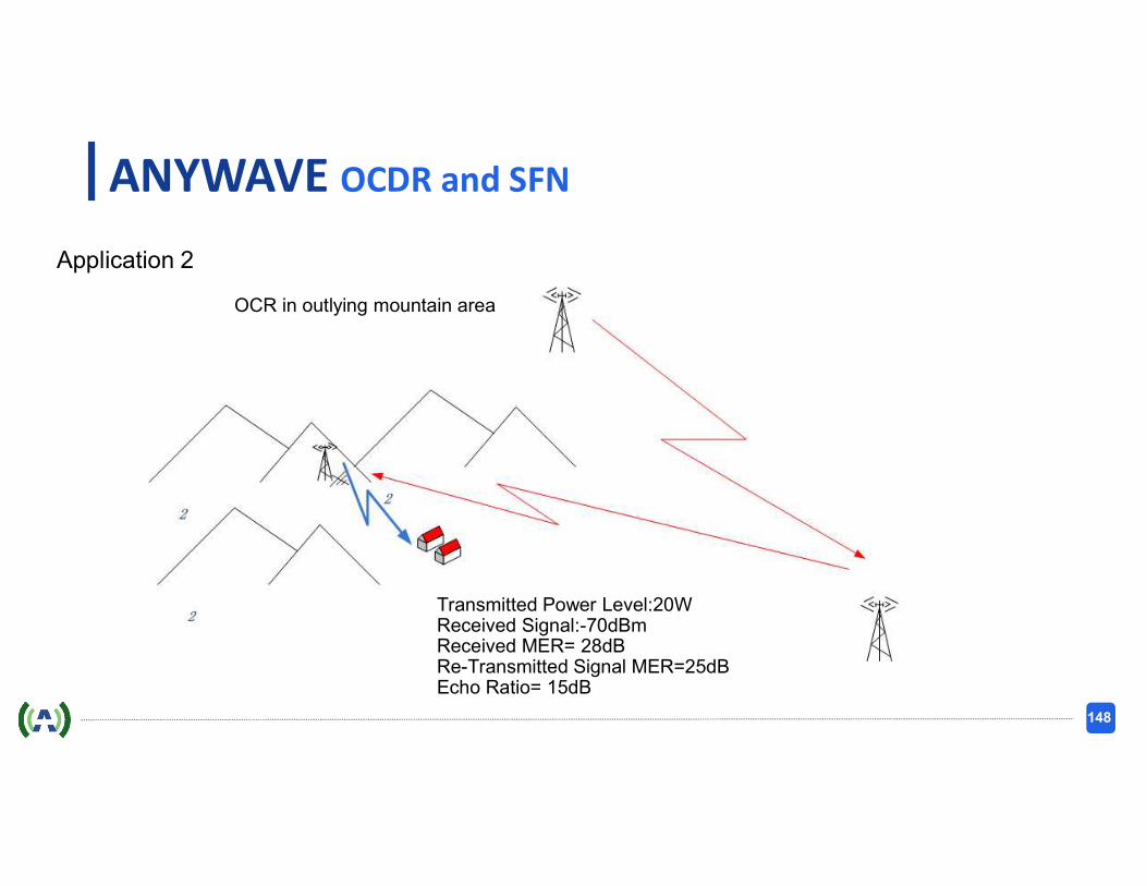
Application 2
OCR in outlying mountain area
Transmitted Power Level:20WReceived Signal:-70dBmReceived MER= 28dBRe-Transmitted Signal MER=25dBEcho Ratio= 15dB
ANYWAVE OCDR and SFN
149
Wideband Broadcasting System (WBS)
For OCRs
ANYWAVE OCDR and SFN

150
Wideband Broadcasting System (WBS)
ANYWAVE OCDR and SFN
A WBS system allows multiple Modulators, Translators and OCDR’s to use the same Power Amplifier
Uses ANYWAVE’s Patented WB PRECORRECTION SYSTEM

151
Advantage of WBS
• Does not require high-power combiner, therefore reduce the complexity and cost of the transmitter
• Easier to change transmitted frequency
• Particularly suitable for low-cost coverage application of multiple channels from the same location
ANYWAVE OCDR and SFN

152
Disadvantage of WBS
Severe distortion without an efficient pre-correction
ANYWAVE OCDR and SFN

153
Wideband Pre-Correction Technology
ANYWAVE OCDR and SFN
With the appropriate Wideband non-linearity correction system Intermodulation distortion can be removed
Result:
Significantly higher output power per amplifier
Improved Non-linearity = better coverage
Example from 5 Inputs / 100W amplifier- without WBCS = 1W- with WBCS = 10W(10dB improvement)

154
SINGLE FREQUENCY NETORKS (SFN)
ANYWAVE OCDR and SFN

155
SFN
ANYWAVE OCDR and SFN
Advantages: - Better use of the frequency spectrum allowing growth for TV channels. - Uniform distribution of radiated power - Distribution increases system availability and reliability. - The presence of multiple transmission points gives the receiver an
- Additive Gain - addition of multiple signals-- and a Statistic Gain - more uniform coverage.
To implement SFN, i.e. synchronize the signals, Key parameters shall be observed: 1. Same transmission Frequency 2. At the same time 3. Same signal (BTS), bit by bit – No rearrangement of the MPEG Stream

156
SFN
ANYWAVE OCDR and SFN
The main parameters that influence a SFN, besides transmitter power are:
• Guard Interval (GI)
• Delay adjustment

157
SFN
ANYWAVE OCDR and SFN
• The GI defines the overlapping area in which an SFN is possible.
• If a receiver falls outside the area protected by the GI and continues to receive signal from more than one transmitter, it won’t be able to open the signal due to inter-symbol interference (ISI).
• i.e. it sees the second signal not as additive but subtractive
• The bigger the Guard Interval the less interference but the lower the bit rate (reduced quality and or reduced number of programs)
1/4
1/8
1/16
1/32
252
126
63
26
76
38
17
8
G/I uS km

158
SFN
ANYWAVE OCDR and SFN
Two transmitters in SFN
If there is no overlap on coverage then there is no interference issues.
TX A TX B

159
SFN
ANYWAVE OCDR and SFN
TX A
• The red area corresponds to the area that can’t be larger than the area in which the delay falls inside the GI.
TX B
• A delay adjustment between transmitters allows the signal to be transmitted at the same time (or with a delay that falls within the GI), allowing the receiver to capture this signal, making a SFN possible.
• Transmitters must be fed with same Broadcast Transport Stream at EXACTLY the same time

160
SFN
ANYWAVE OCDR and SFN
• The delay calculations are made at the generating station
• Calculations have to consider the necessary time for the BTS to arrive at the repeater station
• Once all stations are synchronized the SFN is established.
• This delay calculation can be made manually or automatically.
161
SFN
ANYWAVE OCDR and SFN
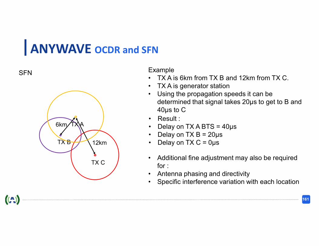
Example• TX A is 6km from TX B and 12km from TX C. • TX A is generator station• Using the propagation speeds it can be
determined that signal takes 20μs to get to B and 40μs to C
TX B
TX C
12km
TX A6km• Result : • Delay on TX A BTS = 40μs• Delay on TX B = 20μs • Delay on TX C = 0μs
• Additional fine adjustment may also be required for :
• Antenna phasing and directivity• Specific interference variation with each location

162
SFN
Example of GI adjustmentTX A + TX B gives interference designated by the yellow area
TX A TX B
ANYWAVE OCDR and SFN
If there is a populated area outside of the GI adjustment area (red circle)
There are two solutions:1. Increase the Guard Interval, but this will reduced the transmission rate (quality and possibly quantity of programs)

163
SFN
• Or adjust the delay to TX B to move the protected area
• Increasing the delay on TX B we make the region where these signals arrive together be closer to the transmitter B This allows the populated area to become protected by the GI.
• There was an intentional delay alteration to move a good reception area from a non-populated area to a more populated one
ANYWAVE OCDR and SFN
TX A TX B

164
SFN
ANYWAVE OCDR and SFN
To further reduce the interference area
• Lower power on the furthest transmitter
• Use of more robust modulation parameters – however, this again will decrease bandwidth and options of programming i.e. only SD instead of HD or UHF.
• Combined use of SFN/MFN, selecting a different channel for one of the stations
• Use of On Channel Digital repeaters in geographically advantageous locations

165
SFN
ANYWAVE OCDR and SFN
• Main SFN components
• An SFN is composed of various equipment's that have specific functions such as BTS generation (encoders), distribution networks (fiber or microwave), delay inserters, modulators (exciters) and synchronization systems.
• None of these additional items are required with OCDR
IMPORTANT: Distribution equipment cannot alter content or packet order in the BTS!
• Equipment used for BTS distribution must be transparent, meaning that the order of the multiplex frame packets is not modified. Equipment used include IP radios, Digital microwave equipment, optic fiber, and satellite links for BTS distribution.

166
SFN
ANYWAVE OCDR and SFN
Network Types: SFN networks can be of two kinds depending on their operation mode: - Dynamic Network
-It is the easiest to implement and the most used configuration, because the delays are calculated automatically with base on the information in the NSI field of the IIP. For this the delay inserters must receive the same 1PPS reference. Maintenace in this type of network is simplified by the automatic calculations for delay, making replacements a simple task with no need to reconfiguration.
Static Network
• In this operation mode the delay calculations are not done by the system and the absolut delay info has to be informed to the Network Adapter (TIME_OFFSET) being necessary only a 10MHz reference for synchronization.
• It is more complex due to the fact that all delays in the distribution channel have to be known in order to configure SFN correctly.

167
SFN
ANYWAVE OCDR and SFN
Dynamic - Pros: Automatic Path Delay calculation - Cons: In case of 1PPS reference failure, transmitter “mutes” not to interfere with whole network.
Static - Pros: No necessity of 1PPS - Cons: Necessary to know all delays in the network. If a piece of equipment is substituted, a new calculation is needed. This info can be obtained from equipment manuals or by measurements.

168
ANYWAVE for all your transmission needs

169
THANK YOU FOR YOUR ATTENTION
ANYWAVE
ANYWAVE COMMUNICATION TECHNOLOGIES CO. LTD
300 KNIGHTSBRIDGE PARKWAY,LINCOLNSHIRE, IL 60069-3655, USA

170
ANYWAVE
ANYWAVE COMMUNICATION TECHNOLOGIES CO. LTD
300 KNIGHTSBRIDGE PARKWAY,LINCOLNSHIRE, IL 60069-3655, USA
SEND US AN [email protected]
CALL US(+66) 83 618-9333
(+1) 847 415 2258 (Ext. 1)
VISIT OUR WEBSITEwww.anywavecom.com/en
For Product Inquiries, please don’t hesitate to contact us.