application note 040 msk5063rh evaluation board user’s guide
TRANSCRIPT

AN040 1
Anaren Microwave, Inc. 6635 Kirkville Road East Syracuse, NY 13057 Phone: 315 432 8909 Fax: 315 432 9121 www.anaren.com
Application Note 040
MSK5063RH Evaluation Board User’s Guide
REV A, 5-12-17
Bryan Horton, Nicole Kresse, Paul Musil Anaren, Inc. –MSK Products
Introduction
The MSK5063RH is a Radiation Hardened wide input voltage range step-down synchronous switching regulator. The
MSK5063RH integrates A RAD HARD Current Mode PWM controller, high and low side RAD HARD Power MOSFETs,
bootstrap supply, and peripheral components in a hermetically sealed in a 46-pin flatpack. The wide input and output
range and feature set make these regulators suitable for many medium to high power applications. The adjustable
operating frequency gives designers flexibility to optimize performance while avoiding sensitive frequency bands.
Synchronization with other switching regulators can be used to reduce EMI and component sizes.
The MSK5063RH Evaluation Board provides a platform from which to evaluate performance and experiment with design
changes for your application. Excessive ripple, instability, and other costly technical problems in flight hardware can be
avoided with evaluation early in the design cycle.
This application note is intended to be used in conjunction with the MSK5063RH data sheet and the LT3845 data sheet.
Reference those documents for additional application information and specifications.
AN040 2
Anaren Microwave, Inc. 6635 Kirkville Road East Syracuse, NY 13057 Phone: 315 432 8909 Fax: 315 432 9121 www.anaren.com
Evaluation Board Setup
Two generic configurations for the MSK5063RH Evaluation Board are detailed herein. Each version is tailored to different
operating regimes. These are simply offered as a starting point for adaptation into a broad range of applications.
The low output voltage configuration operates with 4V ≤ PVIN ≤ 28V; Common for POL applications
The high output voltage configurations operates over 18V ≤ PVIN ≤ 60V; covering the MIL-STD-704F 28VDC bus
There are several possible schemes for supplying power to the MSK5063RH. The optimal approach for any given
application will be depend on available bus voltages, capacities, and the required conversion ratio. VIN, BIAS, and PVIN
input pins can be ganged together or supplied independently. Individual pin ratings must be observed and internal
component power dissipation levels understood. Carefully review the pin functional descriptions and specifications
provided in the MSK5063RH datasheet to ensure the startup and operating requirements are met.
Use the standard turret terminals to connect to your test equipment. Connect a power supply across the Vin and GND
terminals. Connect a power supply to PVIN and PGND terminals. For the low output voltage configuration the BIAS
terminal can be left unconnected or supplied from an external source. For the high output voltage configuration BIAS is
back-fed from the regulated output. Other pin functions are treated separately later in this document.
Connect measurement equipment using Kelvin Sensing techniques to ensure accurate load regulation and efficiency
measurements. The ground wire from an oscilloscope probe acts as an antenna picking up radiated EM fields making
waveforms such as output ripple voltage appear noisy. For improved results, the probe tip can be touched against the
output turret with the bare ground shield pressed against the ground turret.
MODE
The MODE pin connection determines the regulator’s behavior under light loads. Discontinuous Conduction Mode (DCM)
disables the bottom MOSFET gate drive as the inductor current approaches zero thus causing the regulator to behave as
a non-synchronous rectified buck regulator. DCM mode maximizes efficiency at low load current by reducing gate drive
power and conduction losses. Continuous Conduction Mode (CCM) has the benefits of improved noise characteristics,
faster response to large load steps, and does not require a minimum load to maintain tight regulation. Selecting either
mode for the MSK5063RH is as simple as connecting MODE (pin 9) to VFB (pin 8) for DCM or BIAS (pins 12 &13) for CCM.
The MSK5063RH Evaluation board is furnished with a solderless jumper, J1, to allow quick evaluation of either
configuration.
Note: Power down while changing J1.
SHDN
The Eval Board is factory equipped with a 100kΩ resistor pulling the SHDN pin up to VIN. The SHDN pin is internally clamped
to ≈6V and must be current limited to less than 1mA.
A simple Under Voltage Lockout (UVLO) circuit is implemented using just one additional resistors connected from the
SHDN pin to ground. UVLO hysteresis can be increased with a positive feedback resistor from the output to SHDN.

AN040 3
Anaren Microwave, Inc. 6635 Kirkville Road East Syracuse, NY 13057 Phone: 315 432 8909 Fax: 315 432 9121 www.anaren.com
BIAS
The BIAS pins are the output of the internal 8V linear regulator and is sourced from VIN. As with any linear regulator,
efficiency and power dissipation must be considered carefully while operating at large input to output voltage differentials.
Most of the internal control and gate drive circuitry is powered from the BIAS pin node. Internal losses can be reduced by
driving this pin with an external higher voltage source.
The high output voltage version of the Evaluation Card diode OR’s the output to BIAS pins. This approach works well for
applications where the output voltage is greater than ≈8.7V. For output voltages greater than 14V, some means of down
regulating before the BIAS pins is required to remain below the BIAS pin 14V absolute maximum rating. An appropriately
sized Zener diode connected in series with the OR’ing diode is sufficient for this task. Adding a flyback winding to the
output inductor as described below could be a more efficient option.
The low output voltage version of the Evaluation Board is configured to draw BIAS power either directly from VIN through
the internal linear regulator, or back driven from an external supply attached to the BIAS turret. In low output voltage
scenarios, a BIAS supply can be efficiently generated by adding a flyback winding to the output inductor and connecting
one side to either ground or the main output and the other side through a blocking diode to the BIAS pins. Reference the
simplified circuit diagram below.
Figure 1 Simplified Flyback BIAS supply Schematic
COMP
The error amplifier in the MSK5063RH is an Operational Transconductance Amplifier (OTA). The COMP pin is the OTA’s output. Type II compensation is implemented using R4, C11, and C12. C11 sets a pole at the origin, giving high DC gain for reduced regulation error. R4 and C11 form a zero, setting the mid-band gain. C12 sets the high frequency pole. C14 adds an additional zero if needed.
𝑫𝑪 𝒈𝒂𝒊𝒏 = 𝑹𝟐
𝑹𝟏 + 𝑹𝟐 𝒙
𝒈𝒎 × 𝑹𝟒 × 𝑪𝟏𝟏
𝑪𝟏𝟏 × 𝑪𝟏𝟐
𝒇𝒛 = 𝟏
𝟐𝝅 × 𝑹𝟒 × 𝑪𝟏𝟏
𝒇𝒑 = 𝟏
𝟐𝝅 × 𝑹𝟒 × 𝑪𝟏𝟏 × 𝑪𝟏𝟐

AN040 4
Anaren Microwave, Inc. 6635 Kirkville Road East Syracuse, NY 13057 Phone: 315 432 8909 Fax: 315 432 9121 www.anaren.com
Switching Frequency Set Point
The Switching frequency of the MSK5063RH is programmable from
100kHz to 500kHz with a single resistor from the FSET pin to
ground. Both versions of the Evaluation Board are configured for
300kHz operation, R3 = 49.9KΩ. Figure 2 plots the Switching
Frequency vs RSET relationship for quick reference. Choosing the
switching frequency involves balancing efficiency, range of
operation and components sizes. Higher switching frequencies are
generally favored for the substantial savings in filter component
board area at the expense of lower efficiency.
Synchronization and Paralleling
The SYNC pin on the MSK5063RH evaluation board is pulled to GND through a 49.9KΩ resistor. Synchronization eliminates
beat frequency issues that could otherwise occur when multiple switching regulators share a common power bus.
Multiple MSK5063RH modules can be paralleled by synchronizing and connecting the COMP pins. There are several
advantages to paralleling multiple converters compared to a single larger switcher. Inductor size can be considerably
reduced. For example, three 2A inductors store less energy (LI2/2) than one 6A inductor so are far smaller. Synchronizing
three converters 120° out of phase with each other minimizes input and output ripple currents. This reduces the ripple
rating, size and cost of filter capacitors.
Output Voltage Programming
The output voltage is determined by the R1-R2 divider network connected between the Output, VFB pin and GND.
𝑉𝑜𝑢𝑡 = 𝑉𝐹𝐵 × (𝑅1
𝑅2+ 1) 𝑅1 = 𝑅2 × (
𝑉𝑜𝑢𝑡
𝑉𝐹𝐵− 1)
Given: VREF = 1.231V Typ. (3.3V Eval Board): R1 = 2.64kΩ, R2 = 1.57kΩ (15V Eval Board): R1 = 17.56kΩ, R2 = 1.57kΩ
The VFB pin is a high impedance node and is susceptible to noise pickup. Use minimal trace lengths to R1 and R2 and
avoid routing near switching nodes.
Figure 2

AN040 5
Anaren Microwave, Inc. 6635 Kirkville Road East Syracuse, NY 13057 Phone: 315 432 8909 Fax: 315 432 9121 www.anaren.com
Setting the Output Current Limit
R5 senses the inductor current. The maximum peak inductor current (Ioutmax) is approximately 100mV/R5. The maximum
load current is the peak inductor current minus half of the peak-to-peak ripple current. Both versions of the Eval Board
are equipped with a 10mΩ 1W surface mount resistor. Ioutmax for either board is typically greater than 8A across all
conditions.
𝑅5 =100𝑚𝑉
𝐼𝑜𝑢𝑡𝑚𝑎𝑥 + (0.5 × 𝐼𝑟𝑖𝑝𝑝𝑙𝑒)
Inductor Selection
The critical parameters for inductor selection are its value, saturation current specification, Peak Current, and RMS
current. A common starting point for peak to peak current ripple is 20% to 30% of the maximum load current. Use the
following equations to determine the ripple current and RMS current:
∆𝐼 = 𝑉𝑜𝑢𝑡× (𝑉𝐼𝑁−𝑉𝑜𝑢𝑡)
𝐿 ×𝑓𝑠𝑤×∆𝐼 𝐼𝑅𝑀𝑆 = √𝐼𝑜𝑢𝑡
2 +∆𝐼2
12
The control IC has an internal fixed slope compensation ramp. The minimum inductance required to avoid sub-harmonic oscillation is given by:
𝐿𝑚𝑖𝑛 > 𝑉𝑜𝑢𝑡 × 2𝐷𝑚𝑎𝑥 − 1
𝐷𝑚𝑎𝑥×
8.33 × 𝑅𝑆𝐸𝑁𝑆𝐸
𝑓𝑠𝑤
Where: D = Duty Cycle = VOUT/VIN Iout = DC load Current fSW = Switching Frequency 𝜟I = Peal to Peak Ripple current
Provide sufficient derating to prevent saturation and thermal overstress when selecting the inductor.
Input Capacitors
Buck switching regulators are constant power transfer devices and thus exhibit a negative input impedance. That is to say;
as input voltage decreases, input current increases. This has important implication for input filtering and bypass capacitors.
The power bus impedance must be maintained sufficiently below the input impedance of the convertor in order to avoid
control loop interaction or even creation of a negative resistance oscillator. The input bus impedance in many applications
is inductive and will resonant with the regulator’s input capacitors. Adequate damping must be implemented.
The primary factors in selecting the type of input capacitors for any buck switching regulators are the DC voltage rating,
ripple voltage and ripple current ratings. Current is drawn from the input bus in trapezoidal pulses with fast rising edges.
The input ripple current for a buck converter is high; ≈IOUT/2 at 50% duty cycle. Finding capacitors that economically satisfy
all requirements with high reliability is a challenge. Tantalum capacitors in general are not well suited for high voltage and
high ripple current applications. MIL-PRF-49470 series ceramic stack capacitors may be one viable option to consider.
The MSK5063RH Evaluation Board input capacitor selection was geared to work under a very broad range of conditions
and is likely excessive for most real applications.
AN040 6
Anaren Microwave, Inc. 6635 Kirkville Road East Syracuse, NY 13057 Phone: 315 432 8909 Fax: 315 432 9121 www.anaren.com
Output Capacitor Selection
The output capacitors C7 and C8 are AVX TAZ series 47uF tantalum capacitors. See BOM for specific part number. These
capacitors were selected to provide a design starting point using high reliability MIL-PFR-55365/4 qualified capacitors
(CWR). The output capacitor value and its parasitic elements determine several important performance characteristics
including; loop stability and bandwidth, load step response, output ripple voltage start, start-up surge current and output
response due to Single Event Transients.
The output ripple voltage is determined by the inductor ripple current and output capacitor ESR. If lower output ripple
voltage is required, increase the inductor value and/or reduce the ESR by choosing a different capacitor or placing more
capacitors in parallel. For very low ripple, an additional LC filter added to the output may be a more suitable solution. Re-
compensation of the loop may be required if the output capacitance is altered. The output contains very narrow voltage
spikes caused by the parasitic inductance of C7 and C8. Ceramic capacitors C11 and C12 help absorb these spikes on the
demo board. In application, distributed trace impedance and local bypass capacitors will help serve this function.
With current mode control, a single pole is established by the load impedance and output capacitance. ESR of the bulk
output capacitance forms and zero and is exploited to improve phase margin. Ceramic capacitors with equivalent bulk
have comparatively negligible ESR. The impact on loop dynamics should be considered if using large values of ceramic
capacitors. The Evaluation Boards are designed to provide good stability margins over a broad range of applications and
conditions. There is no one size fits all solution, analysis and experimental verification will ensure performance and high
reliability.
Compensation and Measuring Loop Stability
The compensation components on the MSK5063RH evaluation board were selected to provide gain and phase margins
sufficient for many High-Rel applications. Stability margins should be re-assessed after any component change.
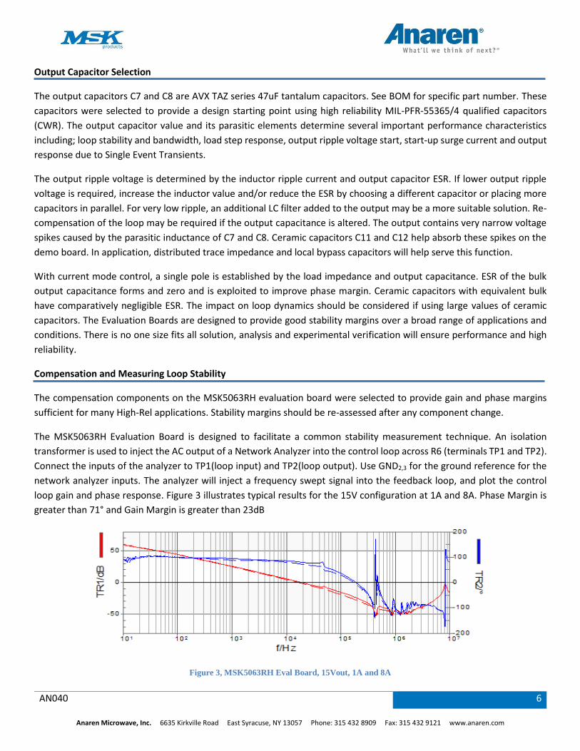
The MSK5063RH Evaluation Board is designed to facilitate a common stability measurement technique. An isolation
transformer is used to inject the AC output of a Network Analyzer into the control loop across R6 (terminals TP1 and TP2).
Connect the inputs of the analyzer to TP1(loop input) and TP2(loop output). Use GND2,3 for the ground reference for the
network analyzer inputs. The analyzer will inject a frequency swept signal into the feedback loop, and plot the control
loop gain and phase response. Figure 3 illustrates typical results for the 15V configuration at 1A and 8A. Phase Margin is
greater than 71° and Gain Margin is greater than 23dB
Figure 3, MSK5063RH Eval Board, 15Vout, 1A and 8A

AN040 7
Anaren Microwave, Inc. 6635 Kirkville Road East Syracuse, NY 13057 Phone: 315 432 8909 Fax: 315 432 9121 www.anaren.com
SWOUT Snubber
Parasitic inductance in the commutating loops and switch node capacitance form a series resonant circuit. The SWOUT
node will ring after every transition at the resonant frequency given by:
𝑓𝑟𝑒𝑠 =1
2𝜋√𝐿𝑠𝐶𝑝.
Good layout practices and component selection can minimize but not eliminate these parasitic elements. Some
applications may require dampening to control the amplitude and frequency of the switch node ring voltage. A dissipative
RC snubber network is commonly used for this task, R7 + C16. The snubber component values can be optimized by first
measuring the ring frequency and then iteratively adding capacitance to the switch node until the ring frequency is
reduced by a factor of .707. This added capacitance is approximately equal to the switch node capacitance. Larger
capacitors will reduce the ring amplitude and frequency at the expense of increased power dissipation.
The resistor value determines how quickly the ringing is damped. A good starting point for the resistor value is set equal
to the snubber capacitor impedance at the ring frequency. Resistor values between 1Ω and 10Ω are common and can be
adjusted as needed. The average power dissipation is equal to the energy stored and released from the snubber
capacitance during a switch cycle, given by:
𝑃𝑠𝑛𝑢𝑏𝑏𝑒𝑟 ≅ 𝐶𝑠𝑛𝑢𝑏𝑏𝑒𝑟 × 𝑃𝑉𝐼𝑁2 × 𝑓𝑆𝑤.
The majority of this power is dissipated in the snubber resistor, be sure to size it appropriately.
Layout Considerations
Switch mode regulators generate very high di/dt and dv/dt
signals in the switching loop components and traces. In many
conditions there is significant energy contained in these high
frequency switching paths.
Figure 4 illustrates a critical high frequency loop. The area
enclosed by this loop should kept as small to minimize
parasitic inductance to EMI.
The lower the impedance of a trace, the less likely it is to be
susceptible to near-field disturbances. Therefore, always
choose the lowest impedance end of a branch for longer
routes. For example consider the feedback divider top
resistor. Given a choice of locating the resistor close to the high impedance error amp input or the low impedance
output, always place it close to the error amp and make the long run to the low impedance output voltage node.
Use ground planes and single point connections to keep a common reference. Make sure components are oriented such
that the signal ground referenced nodes are placed away from regions of high current power ground return paths. The
signal ground reference is the output decoupling capacitors C11 and C12 and GND2.
Figure 4
AN040 8
Anaren Microwave, Inc. 6635 Kirkville Road East Syracuse, NY 13057 Phone: 315 432 8909 Fax: 315 432 9121 www.anaren.com
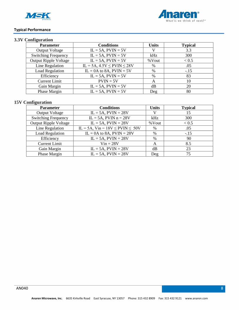
Typical Performance
3.3V Configuration
Parameter Conditions Units Typical Output Voltage IL = 5A, PVIN = 5V V 3.3
Switching Frequency IL = 5A, PVIN = 5V kHz 300 Output Ripple Voltage IL = 5A, PVIN = 5V %Vout < 0.5
Line Regulation IL = 5A, 4.5V ≤ PVIN ≤ 28V % .05 Load Regulation IL = 0A to 8A, PVIN = 5V % -.15
Efficiency IL = 5A, PVIN = 5V % 83 Current Limit PVIN = 5V A 10 Gain Margin IL = 5A, PVIN = 5V dB 20 Phase Margin IL = 5A, PVIN = 5V Deg 80
15V Configuration
Parameter Conditions Units Typical Output Voltage IL = 5A, PVIN = 28V V 15
Switching Frequency IL = 5A, PVIN n = 28V kHz 300 Output Ripple Voltage IL = 5A, PVIN = 28V %Vout < 0.5
Line Regulation IL = 5A, Vin = 18V ≤ PVIN ≤ 50V % .05 Load Regulation IL = 0A to 8A, PVIN = 28V % -.15
Efficiency IL = 5A, PVIN = 28V % 90 Current Limit Vin = 28V A 8.5 Gain Margin IL = 5A, PVIN = 28V dB 23 Phase Margin IL = 5A, PVIN = 28V Deg 75

AN040 9
Anaren Microwave, Inc. 6635 Kirkville Road East Syracuse, NY 13057 Phone: 315 432 8909 Fax: 315 432 9121 www.anaren.com
MSK5063RH Evaluation Board Schematic
MSK5063RH Evaluation Board PCB Artwork
Top Side Bottom Side
AN040 10
Anaren Microwave, Inc. 6635 Kirkville Road East Syracuse, NY 13057 Phone: 315 432 8909 Fax: 315 432 9121 www.anaren.com
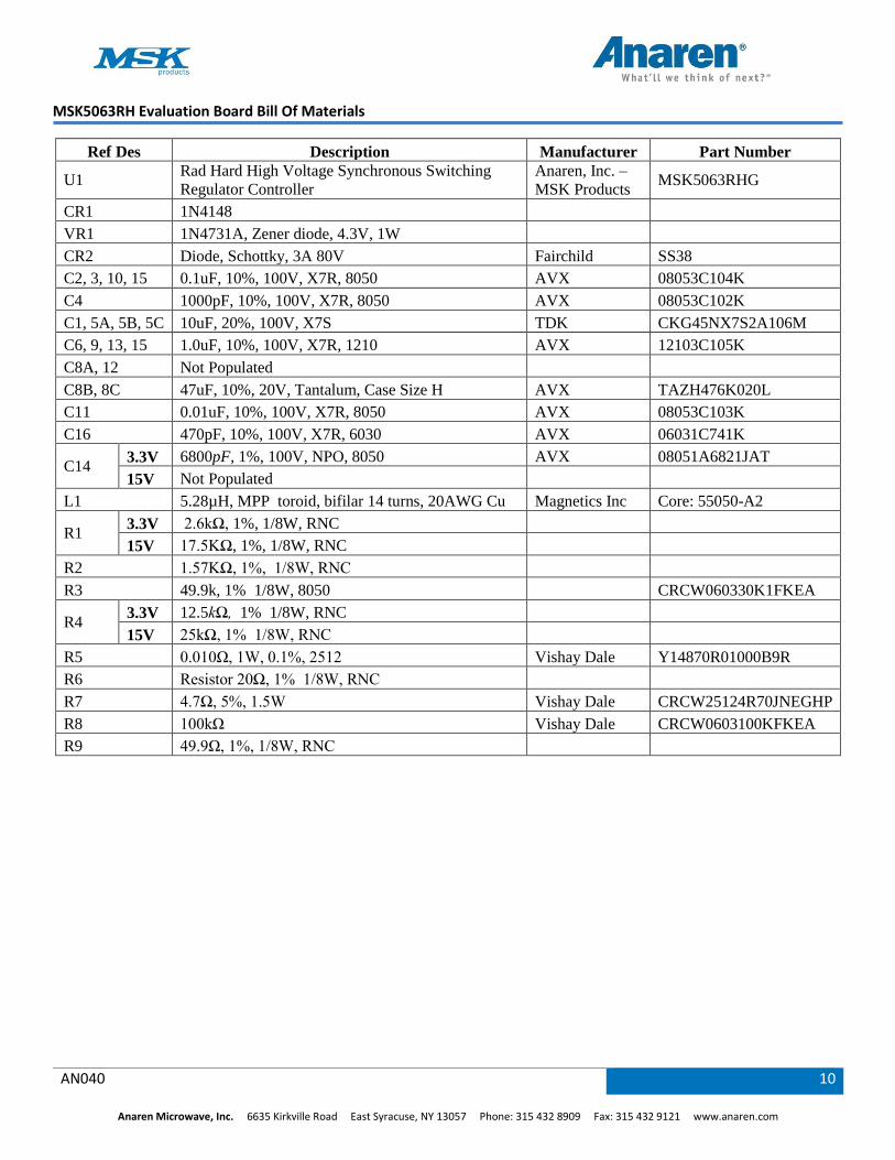
MSK5063RH Evaluation Board Bill Of Materials
Ref Des Description Manufacturer Part Number
U1 Rad Hard High Voltage Synchronous Switching
Regulator Controller Anaren, Inc. –
MSK Products MSK5063RHG
CR1 1N4148
VR1 1N4731A, Zener diode, 4.3V, 1W
CR2 Diode, Schottky, 3A 80V Fairchild SS38
C2, 3, 10, 15 0.1uF, 10%, 100V, X7R, 8050 AVX 08053C104K
C4 1000pF, 10%, 100V, X7R, 8050 AVX 08053C102K
C1, 5A, 5B, 5C 10uF, 20%, 100V, X7S TDK CKG45NX7S2A106M
C6, 9, 13, 15 1.0uF, 10%, 100V, X7R, 1210 AVX 12103C105K
C8A, 12 Not Populated
C8B, 8C 47uF, 10%, 20V, Tantalum, Case Size H AVX TAZH476K020L
C11 0.01uF, 10%, 100V, X7R, 8050 AVX 08053C103K
C16 470pF, 10%, 100V, X7R, 6030 AVX 06031C741K
C14 3.3V 6800pF, 1%, 100V, NPO, 8050 AVX 08051A6821JAT
15V Not Populated L1 5.28µH, MPP toroid, bifilar 14 turns, 20AWG Cu Magnetics Inc Core: 55050-A2
R1 3.3V 2.6kΩ, 1%, 1/8W, RNC
15V 17.5KΩ, 1%, 1/8W, RNC R2 1.57KΩ, 1%, 1/8W, RNC
R3 49.9k, 1% 1/8W, 8050 CRCW060330K1FKEA
R4 3.3V 12.5kΩ, 1% 1/8W, RNC
15V 25kΩ, 1% 1/8W, RNC R5 0.010Ω, 1W, 0.1%, 2512 Vishay Dale Y14870R01000B9R
R6 Resistor 20Ω, 1% 1/8W, RNC
R7 4.7Ω, 5%, 1.5W Vishay Dale CRCW25124R70JNEGHP
R8 100kΩ Vishay Dale CRCW0603100KFKEA
R9 49.9Ω, 1%, 1/8W, RNC

AN040 11
Anaren Microwave, Inc. 6635 Kirkville Road East Syracuse, NY 13057 Phone: 315 432 8909 Fax: 315 432 9121 www.anaren.com
Notes: