application note 5sya 2053-04 applying igbts - abb … · 3 applying igbts i application note 5sya...
TRANSCRIPT

Power and productivityfor a better world™
Due to its controllability, ease of use and high power ratings, the IGBT (Insulated Gate Bipolar Transistor) has become the component of choice for many power electronic applications. It is today possible to build inverters rated to over 1 MW with IGBT modules without paralleling or serial connecting devices, in a common, 2-level voltage source inverter as shown in Fig. 1.To use the IGBT successfully, it is important to understand how both its electrical and thermal parameters are de-fined. The purpose of this application note is to guide and advise potential users with regards to these two aspects and is correspondingly divided into two sections.
Application Note 5SYA 2053-04
Applying IGBTs
Fig 1: 2-level voltage source inverter with IGBTs
2 Applying IGBTs I Application Note 5SYA 2053-04
Page
1 Applying IGBTs 3 1.1 Introduction 3 1.2 Electro-static discharge sensitivity 3
2 Data sheet users guide 3 2.1 Key parameters and features 3 2.2 Maximum rated values 3 2.3 IGBT characteristic values 4 2.4 Diode characteristics 6 2.5 Thermal properties 7 2.6 Mechanical properties 7 2.7 Electrical configuration 7 2.8 Outline drawing 7 2.9 Diagrams 8
3 Power loss and thermal calculations for the IGBT 12 3.1 Calculation methods 12 3.1.1 IGBT loss calculation for two level inverters 12 3.1.2 Diode loss calculation for two level inverters 13 3.1.3 Thermal Calculation 13 3.1.4 Calculations with a Heat sink 14 3.1.5 Transient Overload Calculation 14 3.1.6 IGBT losses calculation for breaking chopper applications 15 3.2 Using the ABB simulation tool 15 3.2.1 Program parts 16 3.2.2 Creating models 20
4 References 22
Contents
3 Applying IGBTs I Application Note 5SYA 2053-04
2.2 Maximum rated valuesMaximum rated values1)
VCES: Collector-emitter voltage. Maximum voltage that under any conditions should be applied between collector and emitter. Applying voltages to the module in excess of this limit, even of short duration, can lead to device failure.The collector – emitter voltage has a temperature dependency. Most ABB devices have been designed to have full blocking voltage within the total operating temperature range but there are a few exceptions where the temperature range across which the rated voltage is valid, is reduced. This is shown in the data sheet at conditions where the temperature range for the rated blocking voltage is specified. For temperatures below the given range, the blocking voltage decreases by about 0.11 percent/K.High DC voltages applied to any semiconductor will provoke high failure rates due to cosmic radiation. For this reason, the operating DC voltage is much lower than the peak repetitive voltage VCES defined above. This is explained and specified in Application Note 5SYA2042. For design voltage recommenda-tions see document 5SYA2051.IC: DC collector current. Maximum DC-current that the IGBT-part of the module can conduct at the given conditions. Exceeding this limit will lead to over-heating of the device.ICM: Peak collector current. Maximum peak current that the IGBT can switch within the limits given in Fig. 11. Exceeding this limit may lead to turn-off failures and (depending on pulse duration) also to over-heating of the device.VGES: Gate-emitter voltage. Absolute maximum allowable voltage between gate and emitter under any conditions. Exceeding the given limits may lead to degradation of the gate oxide, ultimately leading to device failure.
1 IntroductionThe first section is a Data Sheet Users Guide explaining the different parameters and curves included in the ABB IGBT data sheets. The second section describes power loss and thermal calculations of a common PWM-inverter using the ABB simulation tool. Both the data sheets and the simulation tool are available at www.abb.com/semiconductors.Even though the IGBT is a non-latching device it has been designed for switching operation and should not be used in its linear operation mode.This application note does not cover any direct semiconductor physics. For a systematic introduction to the operation principle and physics of power semiconductor devices, including the IGBT, we recommend the book «Power Semiconductors» from Stefan Linder, ISBN 0-8247-2569-7 (CRC Press, published in 2006).
1.2 Electro-static discharge sensitivityThe IGBT is an electrostatic sensitive device and must be handled properly to avoid damage from electro static discharge (ESD). Therefore, please observe the international standard IEC 60747-1 chapter IX. The ABB HiPak-family has been designed and qualified for industrial level.
2 Data sheet users guideThis section is a detailed guide to the proper understanding of an IGBT data sheet. Parameters and ratings will be defined and illustrated by figures, where appropriate, while following the sequence in which parameters appear in the data sheet. For explanation purposes, data and diagrams associated with IGBT type 5SNA 1200E330100 have been used, but because IGBTs have similar data sheets, this guide is applicable to all IGBTs.The data sheets distinguish between maximum rated values and characteristic values. Maximum values indicate limits beyond which damage may occur to the device. Characteristic values are parameters defined under typical application conditions.ABB reserves the right to change data sheets without notice. Therefore, for the latest version, please visit our website at www.abb.com/semiconductors.
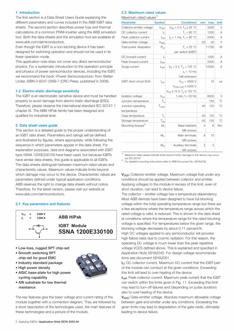
2.1 Key parameters and features
• Low-loss, rugged SPT chip-set • Smooth switching SPT chip-set for good EMC • Industry standard package • High power density • AlSiC base-plate for high power cycling capability • AlN substrate for low thermal resistance
The key features give the basic voltage and current rating of the module together with a connection diagram. They are followed by a short description of the technologies used, the main features of these technologies and a picture of the module.
Parameter Symbol Conditions min max Unit
Collector-emitter voltage VCES VGE = 0 V, Tvj 25 °C 3300 V
DC collector current IC Tc = 80 °C 1200 A
Peak collector current ICM tp = 1 ms, Tc = 80 °C 2400 A
Gate-emitter voltage VGES -20 20 V
Total power dissipation Ptot Tc = 25 °C 11750 W
per switch (IGBT)
DC forward current IF 1200 A
Peak forward current IFRM 2400 A
Surge current IFSM VR = 0 V, Tvj = 125 °C 12000 A
tp = 10 ms
half-sinewave
IGBT short circuit SOA tpsc VCC = 2500 V 10 µs
VCEM CHIP 3300 V
VGE 15 V, Tvj 125 °C
Isolation voltage Visol 1 min, f = 50 Hz 6000 V
Junction temperature Tvj 150 °C
Junction operating Tvj(op) -40 125 °C
temperature
Case temperature Tc -40 125 °C
Storage temperature Tstg -40 125 °C
Mounting torques2) Ms Base-heatsink 4 6 Nm
M6 screws
Mt1 Main terminals 8 10
M8 screws
Mt2 Auxiliary terminals 2 3 M4 screws1)
Maximum rated values indicate limits beyond which damage to the device may occur per IEC 607472)
For detailed mounting instructions refer to ABB Document No. 5SYA2039

4 Applying IGBTs I Application Note 5SYA 2053-04
Ms: Mounting torque base-to-heat-sink. Recommended mounting torque for the bolts fastening the module to the heat sink. For details about mounting see Mounting Instruction 5SYA2039.Mt1: Mounting torque main terminals. Recommended mounting torque for the bolts fastening the bus-bars to the main current terminals. For details about mounting, see Mounting Instruction 5SYA2039. Note that ABB HiPak modules are delivered without mounting bolts for the main terminals. The reason for this is that the correct length of the terminal bolts depends on the user’s bus-bar thickness: an inadequate bolt length will strip the terminal nut threads; an excessive bolt length will puncture the module lid.Mt2: Mounting torque auxiliary terminals. Recommended mounting torque for the bolts fastening the gate unit connections to the control terminals on the module. For details about mounting see Mounting Instruction 5SYA2039.
2.3 IGBT characteristic valuesThe characteristic values are divided into static and dynamic values.
IGBT characteristic values3)
V(BR)CES: Collector (-emitter) breakdown voltage. Minimum voltage that the device will block in the forward direction at the specified conditions.VCEsat: Collector-Emitter saturation voltage. Collector-emitter voltage at the specified conditions. It is given at «chip level» including the resistance in the bonding wires but not including the resistances in the terminals (separately specified).ICES: Collector cut-off current. Collector current at the specified collector-emitter voltage with the gate short-circuited to the emitter.IGES: Gate leakage current. Gate leakage current at the speci-
Ptot: Total power dissipation. Maximum allowed power loss dissipated in the IGBT-part of the module at given conditions. It can be calculated at different case temperatures using Equation 1:
Equation 1
IF: DC forward current. Maximum DC-current that the diode part of the module can conduct at the given conditions. Exceeding this limit will lead to over-heating of the device.IFRM: Peak forward current. Maximum peak current that the diode part of the module can conduct.IFSM: Surge current. Maximum non-repetitive surge current is the maximum allowed pulse-width-dependent peak value of a half-sinusoidal surge current, applied at an instant when the diode is operating at its maximum junction temperature. Though a single surge at the given conditions does not cause any irreversible damage to the module, it should not occur too frequently due to the thermal stress applied to the module during the surge.During a surge, the junction heats up to a temperature well above its rated maximum values such that the diode is no longer able to block rated voltage; the surge current values are therefore only valid when no voltage is reapplied after the surge.tpsc: IGBT Short Circuit SOA. Maximum duration of a short-circuit current pulse through the IGBT at the given conditions. Exceeding this duration will over-heat the device and cause a failure. It determines the limit for the time allowed for possible fault detection and turn-off via the gate unit.Visol: Isolation voltage. Maximum applied voltage between the electrically conductive parts of the module (terminals) and the insulated base plate at the given conditions. All devices are tested at the given conditions before delivery.For insulation coordination purposes, please consult applicable national standards for the equipment’s intended area of use /e.g. IEC 60146.
All ABB modules are in addition to the isolation voltage rated for partial discharge (PD). The used rating is:Ue: Partial discharge extinction voltage. The lowest peak value of the test voltage at which the apparent charge becomes less than the specified discharge magnitude, normally 10 pC at f = 50 hertz tested according to IEC 61287, when the test voltage is reduced below a high level where such discharges have occurred. The de-vice limit is available upon request, if not given in the data sheet.Tvj: Junction temperature. The IGBT and Diode chips used in the module are capable of operating at temperatures up to the specified limit.Tvj(op): Junction operating temperature. The limitation for the operating temperatures mainly emanates from the properties of the organic materials used in the modules. Operating outside the specified temperature window may degrade the module’s materials, leading, for instance, to increased partial discharge.TC: Case temperature. As in the case of Tvj(op), the case tempera-ture must be within the specified limits. This is a smaller restriction than the operating junction temperature since, in practice, the case will always be well below the maximum junction temperature in order to sink the heat.Tstg: Storage temperature. The possible temperature-dependent degradation of the module’s materials may also occur at storage conditions and therefore the storage temperature must be kept within the same limits as the operating temperature.
Parameter Symbol Conditions min typ max Unit
Collector (-emitter) V(BR)CES VGE = 0 V 3300 V
breakdown voltage IC = 10 mA,
Tvj = 25 °C
Collector-emitter4) VCE sat IC = 1200 A
saturation voltage VGE = 15 V
Tvj = 25 °C 2.7 3.1 3.4 V
Tvj = 125 °C 3.5 3.8 4.3 V
Collector cut-off current ICES VCE = 3300 V,
VGE = 0 V
Tvj = 25 °C 12 mA
Tvj = 125 °C 120 mA
Gate leakage current IGES VCE = 0 V -500 500 nA
VGE = ±20 V,
Tvj = 125 °C
Gate-emitter threshold VGE(TO) IC = 240 mA 5.5 7.5 V
voltage VCE = VGE
Tvj = 25 °C
Gate charge Qge IC = 1200 A 12.1 µC
VCE = 1800 V
VGE = -15 V..15 V
Input capacitance Cies VCE = 25 V 187 nF
Output capacitance Coes VGE = 0 V, 11.57
Reverse transfer Cres f = 1 MHz, 2.22
capacitance Tvj = 25 °C
Characteristic values
3) Characteristic values according to IEC 60747 – 9
4) Collector-emitter saturation voltage is given at chip level

5 Applying IGBTs I Application Note 5SYA 2053-04
td(on): Turn-on delay time. The turn-on delay time is defined as the time between the instant when the gate voltage has reached 10 percent of its final value and the instant when the collector current has reached 10 percent of its final value.tr: Rise time. The rise time is defined as the time between instants when the collector current has risen from 10 to 90 percent of its final value.The total turn-on time ton is the sum of td(on) and tr.
td(off): Turn-off delay time. The turn-off delay time is defined as the time between the instant when the gate voltage has dropped to 90 percent of its initial value and the instant when the collector current has dropped to 90 percent of its initial value.tf: Fall time. The fall time is defined as the time between instants when the collector current has dropped from 90to 10 percent of its initial value along an extrapolated straight line drawn between
fied gate-emitter voltage with the collector short-circuited to the emitter.VGE(TO): Gate-Emitter threshold voltage. Gate-emitter voltage at which the collector current attains the specified value.QGE: Gate charge. Charge required to raise the gate voltage from the specified minimum to the specified maximum value of VGE at the given conditions.Cies: Input capacitance. Capacitance between the gate and the emitter terminals with the collector terminal short-circuited to the emitter terminal.Coes: Output capacitance. Capacitance between the collector and the emitter terminals with the gate terminal short-circuited to the emitter terminal.Cres: Reverse transfer capacitance. Capacitance between the collector and the gate terminals.
All switching parameters are defined in a phase-leg connection using an auxiliary component of the same type as the device under test (DUT), see Fig. 2. For the definitions of the different switching parameters, see Figs 3 and 4. All switching parameters in ABB data sheets are specified for an inductive load.Note that other manufacturers may use a different definition for the IGBT switching parameters. This must be considered when comparing modules from different suppliers.
Parameter Symbol Conditions typ Unit
Turn-on delay time td(on) VCC = 1800 V Tvj = 25 °C 400 ns
IC = 1200 A Tvj = 125 °C 400
RG = 1.5
Rise time tr VGE = ±15 V Tvj = 25 °C 175 ns
L = 100 nH, Tvj = 125 °C 200
inductive load
Turn-off delay time td(off) VCC = 1800 V Tvj = 25 °C 940 ns
IC = 1200 A Tvj = 125 °C 1070
RG = 1.5
Fall time tf VGE = ±15 V Tvj = 25 °C 350 ns
L = 100 nH, Tvj = 125 °C 440
inductive load
Turn-on switching Eon VCC = 1800 V Tvj = 25 °C 1340 mJ
energy IC = 1200 A Tvj = 125 °C 1890
VGE = ±15 V
RG = 1.5
L = 100 nH,
inductive load
Turn-off switching Eoff VCC = 1800 V Tvj = 25 °C 1420 mJ
energy IC = 1200 A Tvj = 125 °C 1950
VGE = ±15 V
RG = 1.5
L = 100 nH,
inductive load
Short circuit current ISC tpsc 10 μs, VGE = 15 V, 5000 A
Tvj = 125 °C, VCC = 2500 V,
VCEM CHIP 3300 V
Module stray inductance L CE 10 nH
Resistance, RCC’+EE’ Tvj = 25 °C 0.06 m
terminal-chip Tvj = 125 °C 0.085
Fig. 2: Electrical circuit for testing of the dynamic performance of the IGBT
Fig. 3: Definitions of the turn-on parameters for the IGBT
Fig. 4: Definitions of turn-off parameters for IGBTs

6 Applying IGBTs I Application Note 5SYA 2053-04
VF: Forward voltage. The anode-cathode on-state voltage of the diode at the specified conditions. It is given at chip level and includes bond-wire resistance but not terminal resistance which is separately specified.All switching parameters are defined in a phase leg connection using an auxiliary component of the same type as the device under test (DUT), see Figure 6. For the definitions of the different switching parameters see Figure 7. All switching parameters in the ABB data sheet are specified for inductive load.Note that other manufacturers may use different definitions for diode turn-off parameters. This must be taken into consideration when comparing modules from different suppliers.
Irr: Reverse recovery current. The peak value of the reverse current during commutation at the specified conditions.Qrr: Reverse recovery charge. The integral over time of the reverse current during commutation at the specified conditions starting at the zero-crossing of the current and ending when the reverse current has decayed to zero after the tail-current phase.trr: Reverse recovery time. The commutation time of the diode at the specified conditions. It is measured between the current zero-crossing and the zero-crossing of a straight line drawn between 90 percent of the reverse current peak on the rising flank and 25 percent of peak (on the falling flank).Erec: Reverse recovery energy. The energy dissipated during a single reverse recovery event. It is the integration of the product of the reverse current and voltage from t0 to t1 (see Fig. 7) as expressed by Equation 5.
Eqn 5
the instants when the current has reached 90 and 60 percent of its initial value.The total turn-off time toff is the sum of td(off) and tf.Eon: Turn-on switching energy. The energy dissipated during a single turn-on event. It is the integration of the product of collector current and collector-emitter voltage from t1 to t2 (see Fig. 3) as expressed by Equation 2.
Eqn 2
Eoff: Turn-off switching energy. The energy dissipated during a single turn-off event. It is the integration of the product of the collector current and the collector-emitter voltage from t3 to t4 (see Fig. 4) as expressed by Equation 3.
Eqn 3
ISC: Short circuit current. The self-limited current reached in desaturation when the device is turned on into a short circuit at the specified conditions. Typical waveforms during such an event are shown in Fig. 5. The value shown in the data sheet is the average current during the middle 25 percent of the current pulse.
L CE: Module stray inductance. The internal inductance of the module measured between the collector and emitter terminals.RCC’+EE’: Resistance, terminal-to-chip. The internal resistance of the module measured between the collector and emitter terminals excluding the contribution of the chips and the bond wires. At a given current the voltage drop between the collector and emitter terminals can be calculated using Equation 4.
Eqn 4
2.4 Diode characteristics Diode characteristic values5)
Fig. 5: Typical waveforms for Short-Circuit
Parameter Symbol Conditions min typ max Unit
Forward VF IF = 1200 A Tvj = 25 °C 2.0 2.3 2.6 V
voltage6) Tvj = 125 °C 2.0 2.35 2.6
Reverse reco- Irr Tvj = 25 °C 1100 A
very current VCC = 1800 V Tvj = 125 °C 1350
Recovered Qrr IF = 1200 A, Tvj = 25 °C 715 µC
charge VGE = ±15 V, Tvj = 125 °C 1280
Reverse reco- trr RG = 1.5 Tvj = 25 °C 520 ns
very time L = 100 nH Tvj = 125 °C 1450
Reverse reco- Erec inductive load Tvj = 25 °C 840 mJ
very energy Tvj = 125 °C 1530
5) Characteristic values according to IEC 60747 – 2
6) Forward voltage is given at chip level
Fig. 6: Test circuit for the dynamic performance of the Diode
Fig. 7: Definitions for the turn-off parameters for the Diode

7 Applying IGBTs I Application Note 5SYA 2053-04
2.5 Thermal properties
Rth(j-c)IGBT: IGBT thermal resistance junction to case. The thermal resistance from the IGBT junction (silicon chip) to the case (base plate). Due to the internal layout there are differences in the ther-mal resistance between the various IGBT chips. The value quoted for all IGBT chips together takes this into consideration and allows sufficient margin to ensure that the least-cooled chip does not exceed maximum rated temperature when the calculated operating temperature is within the specified limit.Rth(j-c)DIODE: Diode thermal resistance junction to case. The ther-mal resistance from the Diode junction (silicon chip) to the case (base plate). Due to the internal layout there are differences in the thermal resistance between the different Diode-chips. The value quoted for all Diode chips together takes this into consideration and allows sufficient margin to ensure that the least-cooled chip does not exceed maximum rated temperature when the calcu-lated operating temperature is within the specified limit.Rth(c-s)IGBT: IGBT thermal resistance case to heat sink. The thermal resistance from the case (base plate) to the surface of the heat sink for the part of the case that is heated by the IGBT dies. Since this is a dry interface between two surfaces, only one of which is determined by the semiconductor, the quoted value will be met only if the specification for the heat sink surface, the proper type and application of heat transfer grease and the correct mounting procedures, are fulfilled. For details on heat sink properties and correct mounting procedures, see Document 5SYA2039.Rth(c-s)Diode: Diode thermal resistance case to heat sink. The thermal resistance from the case (base plate) to the surface of the heat sink for the part of the case that is heated by the Diode dies. Since this is a dry interface between two surfaces, only one of which is determined by semiconductor, the quoted value will met only if the specification for the heat sink surface, the proper type and application of heat transfer grease and the correct mounting procedures, are fulfilled. For details on heat sink properties and correct mounting procedures, see Document 5SYA2039.
2.6 Mechanical properties
LxWxH: Dimensions. These values are the main dimensions of the device. Details are found in the outline drawing.da: Clearance distance in air. The air strike distance is defined as the shortest direct path:1) between the terminals and the baseplate2) between terminals.ds: Surface creepage distance. The surface creepage distance is the shortest path along the plastic housing:1) between the terminals and the baseplate2) between the terminals.m: Mass. The weight of the device, excluding packing material.CTI: Comparative tracking index. The CTI of a given insulation material gives a comparative value for the resistance of the material towards the creation of conducting tracks on the surface. The CTI is used for insulation coordination when for instance using IEC 60664. The value is determined using the test method given in IEC 60112. The CTI for the devices are available upon request, if not given in the data sheet.
2.7 Electrical configuration
This figure shows the electrical connection of the module and the internal connections between the different terminals.
2.8 Outline drawingThe outline drawing shows the dimensions of the module with the mechanical tolerances. All dimensions for the ABB-products are in mm.
Parameter Symbol Conditions max Unit
IGBT thermal resistance Rth(j-c)IGBT 0.0085 K/W
junction to case
Diode thermal resistance Rth(j-c)DIODE 0.017 K/W
junction to case
IGBT thermal resistance2) Rth(c-s)IGBT IGBT per switch, K/W
case to heatsink grease = 1W/m x K
Diode thermal resistance7) Rth(c-s)DIODE Diode per switch, K/W
case to heatsink grease = 1W/m x K2)
For detailed mounting instructions refer to ABB Document No. 5SYA20397)
Thermal and mechanical properties according to IEC 60747 – 15
Parameter Symbol Conditions min typ max Unit
Dimensions LxW xH Typical, see outline drawing 190 x 140 x 38 mm
Clearance da according to Term. to base: 23 mm
distance in air IEC 60664-1 Term. to term: 19
and EN 50124-1
Surface ds according to Term. to base: 33 mm
creepage IEC 60664-1 Term. to term: 32
distance and EN 50124-1
Mass m 1380 g7)
Thermal and mechanical properties according to IEC 60747 – 15

8 Applying IGBTs I Application Note 5SYA 2053-04
120.261.20.3 61.20.3
1900.5
18
140
0.5
8.5
59.20.2140.2M4
M8
3 deep48
- 01+
7 0.1
124
0.1
570.11710.15
44
0.2
5
0.2
7
541
0.2
18
0.2
36.50.5380.5
screwing depthmax. 16
screwing depthmax. 8
Label
Outline drawing
Fig. 8: Typical on-state characteristic, chip level
2.9 DiagramsIn addition to the table data a number of diagrams are included showing the most important dependencies of the main parameters.
The on-state voltage for the IGBT is given as a function of the collector current at VGE = 15 V for junction temperatures 25 and 125 °C. Note that the values are shown at chip level which includes the voltage drop in the bond wires but not in the termi-nals. The values are typical.
Fig. 9: Typical transfer characteristic, chip level
The typical transfer characteristic shows the collector current as a function of the gate-emitter voltage for junction temperatures 25 and 125 °C.

9 Applying IGBTs I Application Note 5SYA 2053-04
Fig. 10: Typical output characteristic, chip level
Fig. 11: Typical output characteristic, chip level
Fig. 12: Typical switching energies per pulse vs. collector current
Fig. 13: Typical switching energies per pulse vs. gate resistor
The typical output characteristic shows the collector current as a function of the collector-emitter voltage at gate-emitter voltages of 9, 11, 13, 15 and 17 V for junction temperature 25 °C.
The typical output characteristic shows the collector current as a function of the collector-emitter voltage at gate-emitter voltages of 9, 11, 13, 15 and 17 V for junction temperature 125 °C.
The curves show typical switching energies for the IGBT as a function of the collector current at the specified conditions using the circuit of Fig. 2. Included is a mathematical function for Esw (= Eon + Eoff) as a function of collector current. This func-tion is used in the calculation described in Chapter 3.
The curves show the typical switching energies for the IGBT as a function of the gate resistor at the given conditions using the circuit in figure 2.

10 Applying IGBTs I Application Note 5SYA 2053-04
Fig. 14: Typical switching times vs. collector current
Fig. 15: Typical switching times vs. gate resistor
Fig. 16: Typical capacitances vs collector-emitter voltage
Fig. 17: Typical gate charge characteristics
The curves show typical switching times for the IGBT as a func-tion of the collector current at the specified conditions using the circuit of Fig. 2.
The curves show typical switching times for the IGBT as a func-tion of the gate resistor at the specified conditions using the circuit of Fig. 2.
The curves show typical input, output and transfer capacitances as a function of the collector-emitter voltage at the specified conditions.
The curve shows the typical gate voltage as a function of the gate charge at collector-emitter voltages 1800 V and 2500 V at the given conditions.

11 Applying IGBTs I Application Note 5SYA 2053-04
Fig. 18: Turn-off safe operating area (RBSOA)
Fig. 19: Typical reverse recovery characteristics vs forward current
This curve shows the turn-off safe operating area (RBSOA) of the device at the given conditions for chip and module. Since there will always be an inductance in the turn-off circuit, the device can-not be turned off from a voltage equal or close to VCES since the following criteria for the voltage at turn-off must be fulfilled:
VCEM = di / dt · (Ld CE + Ls) + Vcc VCEs
Thus, VCC in the conditions has to be limited to a value well below VCES.
The curves show typical values of turn-off parameters for the diode as a function of the forward current at the specified condi-tions using the circuit of Fig. 6.
Fig. 20: Typical reverse recovery characteristics vs di/dt
The curves show typical values of turn-off parameters for the diode as a function of the rate of decline of the forward current at the specified conditions using the circuit of Fig. 6. The resistance values indicate the gate resistance for the auxiliary devices giving the corresponding di/dt at the specified conditions.
Fig. 21: Typical diode forward characteristic, chip level
The typical on-state voltage for the Diode is given as a function of the forward current for junction temperatures 25 and 125 °C. Note that the values are shown at chip level which includes the voltage drop in the bond wires but not that in the terminals. The values are typical.

12 Applying IGBTs I Application Note 5SYA 2053-04
The transient thermal impedance emulates the rise of the junction temperature versus time when a constant power is dissipated in the juntion. This function can either be specified as a curve or as an analytic function with the superposition of four exponential terms. The analytic expression is particularly useful for computer calculations.
For detailed information please refer to:• 5SYA 2042-02 Failure rates of HiPak modules due to cosmic rays• 5SYA 2043-01 Load – cycle capability of HiPaks• 5SZK 9120-00 Specification of environmental class for HiPak (available upon request)
At the end of the data sheet, a list of applicable documents is included. See Paragraph 4.1 for information on how to obtain these documents. 3 Power loss and thermal calculations for the IGBTTo assist customers in calculating power losses and junction temperature for ABB IGBTs under various operating conditions, ABB has developed an Excel-based program which is available at www.abb.com/semiconductors. This section describes the calculation methods used in this program as well as guidelines for its use.
3.1 Calculation methodsThe simulation-tool offers a relatively exact and fast method of loss calculation. The data for the IGBT modules are derived from their corresponding data sheets. The calculations are performed
Fig. 22: Safe operating area diode (SOA)
Fig. 23: Thermal impedance vs time
This curve shows the safe operating area (SOA) of the diode at the specified conditions.
with a linear approximation of the devices’ forward characteristics and with a polynomial function for the IGBT and diode switching energies. Additionally, static and switching characteristics are temperature dependent.The power-dissipation calculation for the IGBTs and diodes is executed by an average computation of the conduction and switching losses over one period T0 of the output frequency[1]. This approach yields accurate results for two-level voltage source inverters with naturally sampled PWM and sinusoidal output currents.Additionally a simple approach for loss calculation for a chopper application is shown.For other topologies please refer to simulation tools such as PLECS or GECKO.
3.1.1 IGBT loss calculation for two level inverters:Since the IGBT of one switch conducts only over one half period, the conduction losses are given by the integration of forward losses (VCE0, rCE including RCC’+REE’) up to T0/2:
Eqn 6
with (t) being a function of the pulse pattern (IGBT turned-on: =1 and IGBT turned-off: =0). (t) can be substituted by a
function of modulation (m) and phase angle ( ).
With an infinite switching frequency we deduce the duty cycle variation over time (PWM pattern).
[1] D.Srajber, W.Lukasch, «The calculation of the power dissipation for the IGBT and the
inverse diode in circuits with sinusoidal output voltage», electronica’92, Proc, pp. 51-58

13 Applying IGBTs I Application Note 5SYA 2053-04
Eqn 7
Inserting (t) into the formula and solving the integral we obtain the conduction losses:
Eqn 8
The simulation-tool restricts the modulation index to m 1, which is the linear mode of the PWM.The switching losses are the sum of all turn-on and turn-off energies.The measured turn-on and turn-off energies given in the data sheet can be described as a polynomial function (Esw=f(I)) (see Fig. 12):
Eqn 9
Since the DC-link voltage can vary in different applications, the dependence of the switching energy on the DC-voltage needs to be considered. Within certain limits, this dependence can be assumed to be linear:
Eqn 10
To calculate the switching losses, the switching energies are summed: Eqn 11
where n depends on the switching frequency.
Therefore we calculate the switching losses as a function of phase-current and switching frequency:
Eqn 12
The total IGBT losses are the sum of the conduction and switch-ing losses: Eqn 13
3.1.2 Diode loss calculation for two level invertersThe diode losses are calculated in almost the same way as those of the IGBT. Since the freewheeling diode conducts when the IGBT is turned-off, the function of the pulse pattern has to be negated: Eqn 14
In the case of the diode, the turn-on energy can be disregarded and only the recovery energy counts. The recovery energy given in the data sheet diagram can be described as a polynomial func-tion: Eqn 15
The recovery losses as a function of phase-current and switching frequency and VDC can be written as: Eqn 16
The total diode losses are the sum of the conduction and switch-ing losses: Eqn 17
3.1.3 Thermal CalculationThe loss calculation yields average losses over one output cycle. In fact the losses per switch only occur during one half-period and during the alternate half period, it is the complementary switch which produces losses.Fig. 25 shows, in the upper graph, a PWM chopped current as it appears in the case of a two level VSI. In addition, the resulting junction temperature is shown (as calculated by convolution of instantaneous power loss and thermal impedance). It is obvious that the junction temperature oscillates with the frequency of the output current. In the lower graph the corresponding losses Psmoothed are shown. As a comparison, the calculated average losses (Pav) from the simulation-tool are shown (dashed line).
If the junction temperature is calculated with Tj = Psmoothed * Rth; evidently the peak value of junction temperature exceeds the result of Tj calculated with the average losses Pav. Therefore the calculation of Tj with average losses yields an optimistic value.In order to minimise this inaccuracy, the simulation-tool calculates with Pmod which is twice the average losses (Pav) dissipated during one half period of the phase current. The resulting junction tem-perature Tjmod is shown in the lower graph of Fig. 25 and matches well in terms of the peak and bottom values with the real value of Tj. Nevertheless, at output frequencies below 5 Hz the results of the simplification start to diverge significantly from reality.
The maximum junction temperature Tvj max, as a function of the phase output-current frequency fO, can be calculated if the tran-sient thermal resistance is known:
Eqn 18
with Tref as the reference heat sink temperature, Th for base-less modules or case temperature Tc for based modules.
Fig. 25: Junction temperature as a function of fO

14 Applying IGBTs I Application Note 5SYA 2053-04
3.1.4 Calculations with a Heat sinkThe simulation-tool uses a simplified approach to calculate tem-perature rises and cross-talk effects. This has the advantage that the calculations can be performed using module and heat sink data sheet values.More accurate methods based on finite element calculations require specific knowledge about module and cooler construction and need much more time for parameter extraction as well as for the calculations. On the other hand, the simplified method of the simulation-tool allows quick and accurate simulation without detailed knowledge of cooler and module construction.The simplification in the simulation-tool lies in the assumption of a common reference temperature point, where the temperature is assumed to be homogenous over the full area. This reference is the heat sink temperature (Fig. 26):
The static calculation of the temperature rise in the heat sink can be calculated with the thermal resistance of the cooler and the number of dissipating heat sources mounted on it:
Eqn 19
with nS as the number of switches mounted on the cooler.
For devices with a base-plate, the reference is also the case temperature. The thermal characteristic of a device with a base-plate is normally specified with ZthJC (thermal impedance junction – case) for the IGBT and diode parts. Additionally, the interface resistance case to heat sink (RthCS) is given separately for each IGBT and diode. Fig. 27 shows the thermal equivalent block diagram for modules with a base-plate:
As in the case of baseless modules, the static calculation of the temperature rise in the heat sink can be calculated with the thermal resistance of the cooler and the number of dissipating heat sources mounted on it:
Eqn 20
Additionally the temperature rise in the interface TCH needs to be calculated. Since more than one module may be mounted on the heat sink and the heat sources may be distributed in several modules (e.g. in a three-phase inverter built with three halve-bridge modules mounted on a single cooler) it becomes necessary to scale the interface resistance accordingly: Eqn 21
In order to calculate the temperature-dependent semiconductor losses, the simulation-tool adjusts the junction temperature and the corresponding losses in several iterations. Depending on the module type and the calculation (with/without heat sink), the calculation starts with the initial conditions Tvj = TA, Tvj = TH or Tvj = TC.
3.1.5 Transient Overload CalculationThe simulation-tool offers the possibility to additionally calculate the transient thermal behaviour of the IGBT module and the heat sink.The transient temperature rise can be calculated with the thermal impedance. Eqn 22
The temperature rise T(t) is a function of Zth(t) and the tempera-ture-dependent power dissipation in the semiconductor P(T).
Eqn 23
In order to include the starting conditions for T, the first term is introduced. Tstart / Rth describes the initial constant power that resulted in Tstart. This deposited power influences the thermal behaviour until Zth(t) = Rth(t).The second term describes the heating with the temperature-dependant power P(T). Since T is as well a function of the dissipated power and the thermal impedance, iterations are necessary to obtain an accurate result.
For the transient heat sink temperature we can write:
Eqn 24
where P(T) depends on the number of switches mounted on the heat sink.
Eqn 25
For the transient average junction temperature we can write:
Eqn 26
In the case of modules with a base plate, TH has to be replaced with TC and RthJH and ZthJH have to be replaced with RthJC and ZthJC respectively. In addition, the temperature drop across the interface TCH has to be calculated. Since the interface has no heat capacity, this can be done in a similar manner to the static calculations (Eqn 21).Thus we are able to calculate the transient average junction tem-perature. As already mentioned, the average junction temperature yields overly optimistic values. The temperature ripple as a function of the output current needs to be considered.
Fig. 26: Thermal equivalent block diagram for baseless devices
Fig. 27: Thermal equivalent block diagram for devices with baseplate

15 Applying IGBTs I Application Note 5SYA 2053-04
To avoid too high a complexity, the simulation-tool uses a simplified approach that is valid in most application cases.The approach is to calculate the «overshoot temperature» (Tov) due to the output frequency ripple at the end of the overload pulse and add it to the calculated average temperature:
Eqn 27
Eqn 28
This is valid as long as the Zth(t) of the module is close to its Rth value. For most modules, this is the case between 0.5 and 1s. Below this time span, the values for Tvj max(t) are slightly optimistic. Thus the simulation-tool does not allow transient calculations for durations shorter than 1s.
3.1.6 IGBT losses calculation for breaking chopper applicationsIGBT used in copper applications are usually switching to a breaking resistor. Thus the current is determined by the resistor value and the DC-link voltage. Eqn 29
Fig. 28 shows the schematics of a breaking chopper and the respective switching waveforms in comparison with standard inductive switching. Especially the turn-on losses show a signifi-cant decrease in case of resistive switching. Please note that the showed switching waveforms are for reference purpose only.
Fig. 29 shows the relative switching losses, compared to the standard datasheet conditions with inductive switching versus the parasitic inductance (relative to the datasheet stray inductance) of the chopper resistor (Ls_Rbreak). The turn-on losses (Eon) decrease with higher resistor inductance whereas the turn-off losses (Eoff) are increasing and are approaching the standard inductive switching value for high resistor inductance values. Please note that the shown characteristics are only indicative and need to be verified in the actual application setup.
In order to calculate the losses of the IGBT in chopper mode the chopper current, the duty cycle D = ton / (toff + ton) and the switching frequency fsw = 1/(toff + ton) is required.The conduction losses can be calculated with the duty cycle and the IGBT on-state characteristics:
Eqn 30
The switching losses are depending on the chopper current = ICE and the switching frequency:
Eqn 31
With the factor k the reduction of the losses due to resistive switching compared to inductive switching can be considered (see fig. 29). Eqn 32
3.2 Using the ABB simulation toolThe simulation-tool calculates losses and temperatures for turn-off devices (e.g. IGBTs) and free-wheeling diodes in a PWM 2-level voltage-source inverter (Fig. 30). The results are calculated for one switch. As pointed out in the previous section, the calcula-tion is based on a sinusoidal output current. For other topologies such as 3-level and other control methods, as for instance vector control, direct control etc. the results may no longer be represen-tative. In these cases, it is the user’s sole responsibility to verify whether deviations from the assumptions are still allowable.
Fig. 28: Breaking Chopper schematics and switching waveforms
Fig. 29: Relative switching losses for resistive switching

16 Applying IGBTs I Application Note 5SYA 2053-04
3.2.1 Program partsThe simulation tool has actually four program parts:• Output simple calculation with fixed case-temperature.• Heat sink & Transient Calculation including heat-sink parameters and simulation of transient temperature rises. Calculating heat-flow from main contacts to the bus-bar.• Performance Chart Computes the output-current versus switching frequency that can be achieved for a certain module type at given conditions.• Chopperli Chopper light – a simple sheet to calculate the losses and corresponding junction temperature of an IGBT in chopper applications. (only for Excel 2010 and 2007)• Load Profile Transient simulation of temperatures and losses for a given load profile.
Output:The output program part can compute the junction temperature for given conditions and a fixed case/heat- sink temperature. With the button «Solve», the output current for a given junction temperature Tvj can also be calculated (Fig. 31).The device model can be selected with the drop-down menu in the upper center of the sheet. The required input parameters include: Output Current, DC- Link Voltage, Output Frequency, Switching Frequency, Modulation Index and Load Power Factor. The parameters have to be entered into the yellow shaded fields and are confirmed in the cyan coloured fields provided they are within the necessary boundaries; this is common to all parts of the program. Inverter developers might be troubled by the absence of output voltage as an input parameter for the loss calculations. This is because it is the Modulation Index which
Fig. 31: Calculation of the output voltage at different connections
Fig. 30: Definitions, topology and modulation used in the ABB simulation tool.
The calculated results for one switch are shown in the section “Calculated Results”. Additionally the program offers two dia-grams for the losses and temperatures as a function of output current for one switch (Fig. 33).
M
Io rms
Vdc M
Io rms
Vdc
determines the output voltage (and losses). Nevertheless the output voltage can be calculated for PWM (Fig. 31).

Output DiagramsAverage losses for sinusoidal output current at Tvj = 125°C
5SNA 1200E330100
Temperature gradient and ripple 2 x (Tvj max - Tvj av)
0
1000
2000
3000
4000
5000
6000
7000
8000
0 200 400 600 800 1000 1200 1400 1600 1800Output Current Io rms [A]
Ave
rag
e L
oss
es [
W]
Total switch lossesIGBT total lossesDiode total lossesmax IGBT lossesmax Diode losses
0
10
20
30
40
50
60
70
0 200 400 600 800 1000 1200 1400 1600 1800Output Current Io rms [A]
T [
°C]
DTvj-c IGBTDTvj-c Dioderipple IGBT DTvjripple Diode DTvj
17 Applying IGBTs I Application Note 5SYA 2053-04
Fig. 32: The output sheet
Fig. 33: Curves of losses and temperatures vs. output current
Heat sink & Transient:This part of the program requires identical parameters and works similarly to the Output part (Fig. 34). The main difference is that the heat-sink thermal impedance is included in the calculation. Therefore, a heat sink needs to be selected. If necessary the heat-sink thermal impedance can be adjusted with a multiplier. This might be useful in cases where the area for which Rth is defined does not correspond to the module footprint. It is equally important that the number of operational switches mounted on the same heat sink be entered. For example, in the case of a dual module, n = 2.In addition the heat-flow from the main terminals to the bus-bar (P(T-B)) can be calculated and a warning message appears if the current in the main terminals leads to an overheating of the internal contacts (e.g. rms current in main terminals higher than
recommended).The heat-flow from the terminals to the bus-bar depends on the temperature of the external terminal contact. By default this temperature is set to 105 °C (usual temperature limit of bus-bars). Certainly this temperature strongly depends on the bus-bar design parameters such as cross-section (self-heating), bus-bar cooling and ambient temperature. It is thus strongly rec-ommended to verify this assumption with measurements.In order to enable the tool to calculate the heat-flow and identify too high terminal current, detailed models of the electrical and thermal terminal properties need to be available. This data are stored in the tool library for all HiPak modules.The terminal temperature calculation is no more available in the latest Excel 2010 version of the simulation-tool.

18 Applying IGBTs I Application Note 5SYA 2053-04
Fig. 34: View of the heat sink & transient calculations sheet
Fig. 35: The input fields for the overload calculation
Fig. 36: Output curves showing temperature excursion during the defined overload
For transient overload studies, the temperatures prior to overload and the overload duration need to be specified (Fig. 35).

19 Applying IGBTs I Application Note 5SYA 2053-04
Performance chart:This part of the program computes the inverter output current as a function of the switching frequency (Figs. 37and 38.The switching frequency range of interest can be specified. For easy comparison, up to three modules can be displayed in one chart. The results can be copied into the corresponding columns by pressing the button «Copy Results»:
Fig. 37: The calculation sheet for the performance chart
Fig. 38: Performance chart (results)
Chopperli:Chopper-light: In this sheet the losses of an IGBT in a simple chopper application (resistive switching can be calculated).This function is only available in the version for Excel 2010.
Load profile:This program simulates the transient temperatures and losses of a load profile (Fig. 39). Device model and heat sink have to be selected in the heat sink & transient part of the program.
The load profile can contain up to 10 operation points. For the duration of one operation point, the electrical load remains con-stant. A smooth change in the electrical load can be achieved by splittingit up into several operation points. The result of the simulation is shown in the diagrams of Fig. 40 and can be also extracted as numbers in the output load profile sheet. The data can be used, for example, to calculate life expectancy.

20 Applying IGBTs I Application Note 5SYA 2053-04
3.2.2 Creating modelsThe simulation tool comes complete with an extensive library for most available ABB HiPak modules. The library is regularly up-dated with new products as they become available. Nevertheless, it may be desirable to create one’s own device models. For this reason the simulation tool allows up to three custom models.The necessary parameters are:• Conduction losses at 25 & Tvj(op) – usually 125 °C• Switching losses 25 & Tvj(op) – usually 125 °C• Thermal impedance (junction-case)• Thermal interface resistance (case to heat-sink)
New device models can be specified in the section input.The following Figs. 41 to 46 describe how a model can be generated:
Fig. 39: Input fields for the load profile calculation
Fig. 40: Load profile calculation results in form of a temperature diagram
Fig. 41: Input fields for the general description of the module

21 Applying IGBTs I Application Note 5SYA 2053-04
Fig. 44: Input fields for the internal resistance and the thermal impedance
Fig. 43: Input fields for the diode loss characteristics
Fig. 42: Input fields for the IGBT loss characteristics

Power and productivityfor a better world™
App
licat
ion
note
5S
YA 2
053
05
.09.
2013
NoteWe reserve the right to make technical changes or to modify the contents of this document without prior notice.We reserve all rights in this document and the information con-tained therein. Any reproduction or utilisation of this document or parts thereof for commercial purposes without our prior writtenconsent is forbidden.Any liability for use of our products contrary to the instructions in this document is excluded.
Form more Informations:ABB Switzerland LtdSemiconductorsFabrikstrasse 3CH-5600 LenzburgSwitzerlandTel: +41 58 586 14 19Fax: +41 58 586 13 06E-Mail: [email protected]/semiconductorsm.abb.com
Fig. 45: Input fields for the polynomial approximation of the switching losses
Fig. 46 Input fields for the thermal resistance case to heat-sink and a description how to
deal with devices without base plate
Version Change Authors
04 Björn Backlund
Raffael Schnell
Ulrich Schlapbach
Roland Fischer
Evgeny Tsyplakov
4 References1) IEC 60146 «Semiconductor convertors»2) IEC 60664-1 (1992) «Insulation Co-ordination Within Low-Voltage Systems»3) IEC 60747 «Semiconductor Devices»4) 5SYA2039 «Mounting instructions for HiPak Modules5) 5SYA2042 «Failure rates of HiPak modules due to cosmic ray»6) 5SYA2043 «Load cycling capability of HiPaks»7) 5SYA2045 «Thermal runaway during blocking»8) 5SYA2051 «Voltage ratings of high power semiconductors»9) 5SYA2057 «IGBT Diode SOA»10) 5SYA2058 «Surge currents for IGBT Diodes»11) 5SYA2093 «Thermal Design and Temperature Ratings of IGBT Modules»12) 5SZK9120 «Specification of environmental class for HiPak, Operation (Traction)»The application notes, references 4 - 10, are available at www.abb.com/semiconductors. The environmental specification, reference 11, is available upon request.
6 Revision history